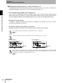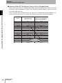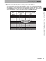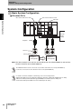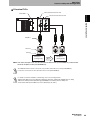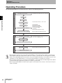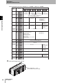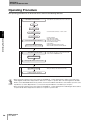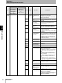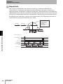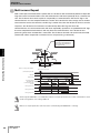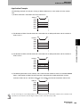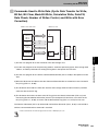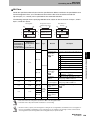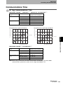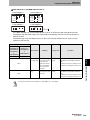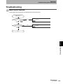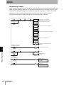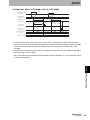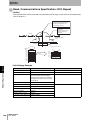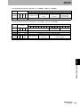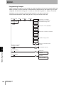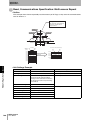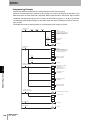
1
RFID System V680 Series User’s Manual ID Sensor Units CS1W-V680C11 CS1W-V680C12 CJ1W-V680C11 CJ1W-V680C12 P ER H ER D2 A HE T/R /ERR 1 C1 80 V6 RUN C ER 1 AD HE /R T RM NO RM NO R R /ER /ER RM RM NO NO TE P ER H ER D2 A HE T/R /ERR 2 C1 80 V6 RUN C ER 1 AD HE /R T ST TE ON ST ON HE AD HE HE AD 1 AD 2 V 24 DC UT P IN + - Man. No.: Z271-E1-03 Introduction Thank you for purchasing an ID Sensor Unit for a V680-series RFID System. This manual describes the functions, performance, and application methods needed for optimum use of your V680-series RFID System. Please observe the following items when using the V680-series RFID System. • Allow the V680-series RFID System to be installed and operated only by qualified specialist with a sufficient knowledge of electrical systems. • Read and understand this manual before attempting to use the V680-series RFID System and use the V680-series RFID System correctly. • Keep this manual in a safe and accessible location so that it is available for reference when required. READ AND UNDERSTAND THIS DOCUMENT Section 1 Features and System Configuration Introduction SECTION 1 Introduction Section 2 CS-series ID Sensor Units SECTION 2 Section 3 CJ-series ID Sensor Units SECTION 3 Section 4 Data Exchange with the CPU Unit SECTION 4 Section 5 ID Sensor Unit Functions SECTION 5 Section 6 Controlling the ID Sensor Unit SECTION 6 Section 7 Troubleshooting Alarms and Errors SECTION 7 Section 8 Appendices SECTION 8 RFID System CS1W-V680C11 CS1W-V680C12 CJ1W-V680C11 CJ1W-V680C12 ID Sensor Unit ID Sensor Unit ID Sensor Unit ID Sensor Unit User's Manual Introduction Introduction READ AND UNDERSTAND THIS DOCUMENT Please read and understand this document before using the products. Please consult your OMRON representative if you have any questions or comments. READ AND UNDERSTAND THIS DOCUMENT WARRANTY OMRON’s exclusive warranty is that the products are free from defects in materials and workmanship for a period of one year (or other period if specified) from date of sale by OMRON. OMRON MAKES NO WARRANTY OR REPRESENTATION, EXPRESS OR IMPLIED, REGARDING NONINFRINGEMENT, MERCHANTABILITY, OR FITNESS FOR PARTICULAR PURPOSE OF THE PRODUCTS. ANY BUYER OR USER ACKNOWLEDGES THAT THE BUYER OR USER ALONE HAS DETERMINED THAT THE PRODUCTS WILL SUITABLY MEET THE REQUIREMENTS OF THEIR INTENDED USE. OMRON DISCLAIMS ALL OTHER WARRANTIES, EXPRESS OR IMPLIED. LIMITATIONS OF LIABILITY OMRON SHALL NOT BE RESPONSIBLE FOR SPECIAL, INDIRECT, OR CONSEQUENTIAL DAMAGES, LOSS OF PROFITS OR COMMERCIAL LOSS IN ANY WAY CONNECTED WITH THE PRODUCTS, WHETHER SUCH CLAIM IS BASED ON CONTRACT, WARRANTY, NEGLIGENCE, OR STRICT LIABILITY. In no event shall responsibility of OMRON for any act exceed the individual price of the product on which liability is asserted. IN NO EVENT SHALL OMRON BE RESPONSIBLE FOR WARRANTY, REPAIR, OR OTHER CLAIMS REGARDING THE PRODUCTS UNLESS OMRON’S ANALYSIS CONFIRMS THAT THE PRODUCTS WERE PROPERLY HANDLED, STORED, INSTALLED, AND MAINTAINED AND NOT SUBJECT TO CONTAMINATION, ABUSE, MISUSE, OR INAPPROPRIATE MODIFICATION OR REPAIR. SUITABILITY FOR USE THE PRODUCTS CONTAINED IN THIS DOCUMENT ARE NOT SAFETY RATED. THEY ARE NOT DESIGNED OR RATED FOR ENSURING SAFETY OF PERSONS, AND SHOULD NOT BE RELIED UPON AS A SAFETY COMPONENT OR PROTECTIVE DEVICE FOR SUCH PURPOSES. Please refer to separate catalogs for OMRON's safety rated products. OMRON shall not be responsible for conformity with any standards, codes, or regulations that apply to the combination of products in the customer’s application or use of the product. At the customer’s request, OMRON will provide applicable third party certification documents identifying ratings and limitations of use that apply to the products. This information by itself is not sufficient for a complete determination of the suitability of the products in combination with the end product, machine, system, or other application or use. The following are some examples of applications for which particular attention must be given. This is not intended to be an exhaustive list of all possible uses of the products, nor is it intended to imply that the uses listed may be suitable for the products: • Outdoor use, uses involving potential chemical contamination or electrical interference, or conditions or uses not described in this document. • Nuclear energy control systems, combustion systems, railroad systems, aviation systems, medical equipment, amusement machines, vehicles, safety equipment, and installations subject to separate industry or government regulations. • Systems, machines, and equipment that could present a risk to life or property. Please know and observe all prohibitions of use applicable to the products. NEVER USE THE PRODUCTS FOR AN APPLICATION INVOLVING SERIOUS RISK TO LIFE OR PROPERTY WITHOUT ENSURING THAT THE SYSTEM AS A WHOLE HAS BEEN DESIGNED TO ADDRESS THE RISKS, AND THAT THE OMRON PRODUCT IS PROPERLY RATED AND INSTALLED FOR THE INTENDED USE WITHIN THE OVERALL EQUIPMENT OR SYSTEM. 2 RFID System User's Manual Introduction Introduction PERFORMANCE DATA READ AND UNDERSTAND THIS DOCUMENT Performance data given in this document is provided as a guide for the user in determining suitability and does not constitute a warranty. It may represent the result of OMRON’s test conditions, and the users must correlate it to actual application requirements. Actual performance is subject to the OMRON Warranty and Limitations of Liability. CHANGE IN SPECIFICATIONS Product specifications and accessories may be changed at any time based on improvements and other reasons. It is our practice to change model numbers when published ratings or features are changed, or when significant construction changes are made. However, some specifications of the product may be changed without any notice. When in doubt, special model numbers may be assigned to fix or establish key specifications for your application on your request. Please consult with your OMRON representative at any time to confirm actual specifications of purchased products. DIMENSIONS AND WEIGHTS Dimensions and weights are nominal and are not to be used for manufacturing purposes, even when tolerances are shown. ERRORS AND OMISSIONS The information in this document has been carefully checked and is believed to be accurate; however, no responsibility is assumed for clerical, typographical, or proofreading errors, or omissions. PROGRAMMABLE PRODUCTS OMRON shall not be responsible for the user’s programming of a programmable product, or any consequence thereof. COPYRIGHT AND COPY PERMISSION This document shall not be copied for sales or promotions without permission. This document is protected by copyright and is intended solely for use in conjunction with the product. Please notify us before copying or reproducing this document in any manner, for any other purpose. If copying or transmitting this document to another, please copy or transmit it in its entirety. RFID System User's Manual 3 Introduction Introduction Safety Precautions READ AND UNDERSTAND THIS DOCUMENT z Signal Words Used in This Manual The following signal words and symbols are used in this manual to indicate precautions that must be observed to ensure safe use of the V680-series ID Sensor Unit. The precautions provided here contain important safety information. You must observe these precautions. The following signal words and symbols are used in this manual. WARNING Indicates a potentially hazardous situation which, if not avoided, will result in minor or moderate injury, or may result in serious injury or death. Additionally there may be significant property damage. CAUTION Indicates a potentially hazardous situation which, if not avoided, may result in minor or moderate injury or in property damage. z Meanings of Alert Symbols General Caution Indicates general cautionary, warning, or danger level information. Electrical Shock Caution Indicates possibility of electric shock under specific conditions. General Prohibition Indicates a general prohibition. Disassembly Prohibition Indicates that disassembly is prohibited to prevent electric shock. General Mandatory Action Indicates a general action that must be performed by the user. 4 RFID System User's Manual Introduction Introduction z Warnings READ AND UNDERSTAND THIS DOCUMENT WARNING Never attempt to disassemble any Units while power is being supplied. Doing so may result in serious electrical shock or electrocution. Never touch any of the terminals while power is being supplied. Doing so may result in serious electrical shock or electrocution. Provide safety measures in external circuits, l.e., not in the PLC (CPU Unit including associated Units), in order to ensure safety in the system if an abnormality occurs due to malfunction of the PLC or another external factor affecting the PLC operation. Not doing so may result in serious accidents. •Emergency stop circuits, interlock circuits, limit cuicuits, and similar safety measures must be provided in external control circuits. •The PLC will turn OFF all outputs when its self-diagnosis function detects any error or when a severe failure alarm (FALS) instruction is executed. As a countermeasure for such errors, external safety measures must be provided to ensure safety in the system. •The PLC outputs may remain ON or OFF due to deposition or burning of the output relays or destruction of the output transistors, As a countermeasure for such problems, external safety measures must be provided to ensure safety in the system. This Product is not designed or rated for ensuring safety of persons. Do not use it for such purposes. CAUTION Execute online edit only after confirming that no adverse effects will be caused by extending the cycle time. Otherwise, the input signals may not be readable. RFID System User's Manual 5 Introduction Introduction Regulations and Standards READ AND UNDERSTAND THIS DOCUMENT The V680-series ID Sensor Unit conforms to the following international regulations and standards. 1. EMC Standards The V680-series ID Sensor Unit meets EMC requirements. EMC Standard: EN 61000-6-2 EN 61000-6-4 Connect to either circuit type (1) or (2) listed below. (1) Limited Voltage/Current Circuit (Approved under UL 508) A circuit that uses the secondary windings of an isolation transformer as its power supply and fulfills the following conditions: • Maximum voltage (with no load): 30 Vrms (42.4 V peak) and • Maximum current: (a) 8 A (including short-circuits) or (b) Current limited by a circuit protection device (e.g., fuse) with the ratings listed in the following table. No-load voltage (Vrms) Maximum current rating (A) 0 to 20 5.0 Over 20 to 30 100 Peak voltage (2) A class 2 circuit with a maximum voltage of 30 Vrms (42.4 V peak) that uses a class 2 power supply conforming to UL 1310 or a class 2 transformer conforming to UL 1585 as its power source. 6 RFID System User's Manual Introduction Introduction Precautions for Safe Use READ AND UNDERSTAND THIS DOCUMENT Be sure to observe the following precautions to ensure safe use of the Product. 1. Do not attempt to disassemble, repair, or modify the Product. 2. Tighten the Backplane mounting screws and terminal block screws securely. 3. Be sure to use crimp terminals of the specified size for wiring. 4. If any cable has a locking mechanism, make sure that it has been locked before using the cable. 5. Make sure the power supplied by the DC Power Supply Unit is within the rated power supply voltage (24 VDC +10%/−15%) before using the Product. 6. When using the CS1W-V680C12, make sure the power supplied by the DC power supply for external inputs is within the rated power supply voltage (24 VDC +10%/−15%) before using the Product. 7. Do not connect the power supply in reverse. 8. Use crimp terminals for wiring. Do not connect bare stranded wires directly to terminals. 9. Do not allow water or wires to enter the Product through gaps in the case. Otherwise, fire or electric shock may occur. 10. Turn OFF the power to the Product before attaching or removing an Amplifier or Antenna. 11. If multiple Antennas are mounted near each other, communications performance may decrease due to mutual interference. Refer to information on installing Antenna in the RFID System V680 Series User's Manual for Amplifiers, Antennas, and RF Tags (FRAM) (Cat. No. Z248), V680 Series RFID System Amplifier/RF Tags (EEPROM) User's Manual (Cat. No. Z262), and Heat-resistive RFID System V680 Series User's Manual (Cat. No. Z221) and check to make sure there is no mutual interference. 12. If an error is detected in the Product, immediately stop operation and turn OFF the power supply. Consult with an OMRON representative. 13. Dispose of the Product as industrial waste. 14. Observe all warnings and precautions given in the body of this manual. 15. Do not use thinners, benzenes, acetones, and kerosenes for cleaning. RFID System User's Manual 7 Introduction Introduction Precautions for Correct Use READ AND UNDERSTAND THIS DOCUMENT Always observe the following precautions to prevent operation failure, malfunctions, and adverse effects on performance and equipment. 1. Installation Environment Do not use the Product in the following locations. • Locations exposed to any flammable, explosive, or corrosive gasses • Locations exposed to dust, metallic powder, or salts • Locations not within the specified operating temperature range • Locations subject to rapid changes in temperature or condensation • Locations not within the specified operating humidity range • Locations subject to direct vibration or shock outside the specified ranges • Locations subject to spray of water, oil, or chemicals 2. Installation • This Product uses a frequency band of 13.56 MHz to communicate with RF Tags. Some transceivers, motors, inverters, switching power supplies, etc., generate electrical noise that will affect these communications. If any of these devices are located in the vicinity of the Product, they may affect communications with RF Tags, and may possibly damage the RF Tags. Prior to using the Product in the vicinity of any of these devices, perform a test to determine whether the Product can be used under the resulting influence. • Observe the following precautions to minimize the effects of normal noise. (1) Ground the ground terminal on the Product and all metal objects in the vicinity of the Product to 100 Ω or less. (2) Do not use the Product near high-voltage or high-current lines. • The Product is not waterproof. Do not use it in an environment where mist is present. • Do not expose the Product to chemicals that adversely affect the Product materials. • Use a tightening torque of 0.4 N⋅m hen mounting the Product. 3. Storage • Locations exposed to any flammable, explosive, or corrosive gasses • Locations exposed to dust, metallic powder, or salts • Locations not within the specified operating temperature range • Locations subject to rapid changes in temperature or condensation • Locations not within the specified operating humidity range • Locations subject to direct vibration or shock outside the specified ranges • Locations subject to spray of water, oil, or chemicals 8 RFID System User's Manual Introduction Introduction Precautions for Users of V600-series ID Sensor Units Precautions for Users of V600-series ID Sensor Units Differences between the V600-series and V680-series ID Sensor Units The following features were added to the V680-series ID Sensor Units in comparison to the V600series Units. Functions are upwardly compatible, so V600-series Units can be easily replaced with V680-series Units. Commands • Read with Error Correction • Write with Error Correction • UID Read • Noise Measurement Communications specifications • FIFO trigger • FIFO repeat • Multi-access trigger • Multi-access repeat DM Area settings • UID Addition Setting • Write Protection Disable Setting • Antenna Connection Setting (V680-H01) • Results Monitor Output Setting • Test Operation Setting • Run/Test Switching Method Setting Test Operations (Set in the DM Area) • Distance level measurement • Read/Write speed level measurement • Noise level measurement • Communications success rate measurement CIO Area outputs Run/Test Bit (Only when using the Run/Test Switching Method Setting is enabled in the DM Area.) CIO Area inputs • Antenna Error Flag (9C) • ID System Error 1 (79) • ID System Error 2 (7E) • ID System Error 3 (7F) • Error Correction Flag (77) • Results Output Monitor Run Mode: Communications time or noise level Test Mode: Result contents of tests Others If a command error or data storage area error occurs in a V600-series ID Sensor Unit, the Error End Flag will not be turned ON. With a V680-series ID Sensor Unit, the Error End Flag will be turned ON for these errors. ∗ FIFO trigger, FIFO repeat, Multi-access trigger, and Multi-access repeat specification cannot be used for communicating with V680-D1KP@@ RF Tags. With a V600-series ID Sensor Unit, command errors and data storage errors are not monitored in the Processing Results Monitor, but a V680-series ID Sensor Unit will monitor them and use an error code of E014. RFID System User's Manual 9 Introduction Introduction Meanings of Symbols 10 Meanings of Symbols Indicates particularly important points related to a function, including precautions and application advice. Indicates page numbers containing relevant information. Indicates reference to helpful information and explanations for difficult terminology. RFID System User's Manual Introduction Introduction Table of Contents Introduction 1 READ AND UNDERSTAND THIS DOCUMENT 2 Safety Precautions 4 Regulations and Standards 6 Precautions for Safe Use 7 Precautions for Correct Use 8 Precautions for Users of V600-series ID Sensor Units 9 Meanings of Symbols 10 Table of Contents 11 Features and System Configuration 13 Outline of Features and Functions 14 Using Heat-resistive RF Tags (V680-D1KP58HTN and V680-D1KP58HT) 17 System Configuration 22 Functions by Application 28 CS-series ID Sensor Units 29 Specifications 30 Operating Procedure 32 Part Names and Functions 38 Connections and Wiring 41 CJ-series ID Sensor Units 45 Specifications 46 Operating Procedure 48 Part Names and Functions 54 Connections and Wiring 57 Data Exchange with the CPU Unit 61 Outline of Data Exchange 62 Initial Settings Data 65 I/O Data Allocations 67 RFID System User's Manual 11 Introduction Introduction ID Sensor Unit Functions Operating Modes 78 Communications Specifications 85 Parameter Settings in DM Area 93 RF Tag Memory 99 Write Protection 101 RF Tag Service Life Check 108 RF Tag Memory Check 112 RF Tag Memory Error Correction 114 Controlling the ID Sensor Unit 117 ID Sensor Unit Operation 118 Communications Commands 125 Communications Time 141 Troubleshooting Alarms and Errors 145 Indicators and Error Check Flowcharts 146 ID Sensor Unit Alarms 148 CPU Unit Errors 151 Restarting Special I/O Units 152 Troubleshooting 153 Appendices 157 Dimensions 158 Sample Programming 160 Data Coding Tables 204 Degree of Protection 208 Revision History 12 77 RFID System User's Manual 210 SECTION 1 SECTION 1 Features and System Configuration 14 Using Heat-resistive RF Tags (V680-D1KP58HTN and V680-D1KP58HT) 17 System Configuration 22 Functions by Application 28 RFID System User's Manual Features and System Configuration Outline of Features and Functions 13 SECTION 1 Features and System Configuration Outline of Features and Functions • SYSMAC CS-series ID Sensor Units SECTION 1 One-channel ID Sensor Unit Two-channels ID Sensor Unit (CS1W-V680C11) (CS1W-V680C12) Outline of Features and Functions V680C11 RUN ERC ERP ERH T/R V680C12 RUN ERC HEAD1 T/R ERP ERH HEAD2 T/R NORM/ERR NORM/ERR TEST NORM/ERR TEST ON ON HEAD1 HEAD HEAD2 DC24V INPUT These ID Sensor Units are used in SYSMAC CS-series PLCs to read and write data for V680-series RF Tags. There are two models: a One-channel ID Sensor Unit (CS1W-V680C11) and a Two-channels ID Sensor Unit (CS1W-V680C12). 14 RFID System User's Manual SECTION 1 Features and System Configuration • SYSMAC CJ-series ID Sensor Units Two-channels ID Sensor Unit (CJ1W-V680C11) (CJ1W-V680C12) SECTION 1 One-channel ID Sensor Unit Outline of Features and Functions These ID Sensor Units are used in SYSMAC CJ-series PLCs to read and write data for V680-series RF Tags. There are two models: a One-channel ID Sensor Unit (CJ1W-V680C11) and a Two-channels ID Sensor Unit (CJ1W-V680C12). CS1W-V680C11 CS1W-V680C12 Amplifier/ Antennas V680 Series (V680-HA63@/V680-H@@) Maximum number of connected Antennas 1 2 RF Tags V680 Series (V680-D@@F@@ or V680-D@@P@@) Commands Read Write Bit Set Bit Clear Mask Bit Write Calculation Write Data Fill Data Check Number of Writes Control Read with Error Correction Write with Error Correction UID Read Noise Measurement Read Write Bit Set Bit Clear Mask Bit Write Calculation Write Data Fill Data Check Number of Writes Control Copy Read with Error Correction Write with Error Correction UID Read Noise Measurement CJ1W-V680C11 CJ1W-V680C12 1 2 Read Write Bit Set Bit Clear Mask Bit Write Calculation Write Data Fill Data Check Number of Writes Control Read with Error Correction Write with Error Correction UID Read Noise Measurement Read Write Bit Set Bit Clear Mask Bit Write Calculation Write Data Fill Data Check Number of Writes Control Copy Read with Error Correction Write with Error Correction UID Read Noise Measurement • An RFID system consists of an ID Sensor Unit in a CS-series/CJ-series CPU Rack or CS-series/CJ-series Expansion Rack, one or two Antennas connected to the ID Sensor Unit, and RF Tags connected to moving bodies. • The ID Sensor Unit operates through the Antennas to write data from the CS/CJ-series CPU Unit to the RF Tags and read data from the RF Tags to the CS/CJ-series CPU Unit. RFID System User's Manual 15 SECTION 1 Features and System Configuration ■ Differences between Version 1.2 and Pre-Version 1.2 The following functions have been added to version 1.2 in comparison to pre-version 1.2. Functions are upwardly compatible, so pre-version 1.2 can be replaced with version 1.2. SECTION 1 CA1D Mode Setting Added for RF Tag Memory If you are using a V680-CA1D/-CA2D ID Controller, always set the RF Tag memory setting to CA1D Outline of Features and Functions Mode. Setting the RF Tag memory setting to CA1D Mode enables reading and writing Heat-resistant RF Tags (V680-D1KP58HTN and V680-D1KP58HT) that were written by the V680-CA1D/-CA2D. New Data Transfer Setting In addition to cyclically transferring 160 bytes/scan, Intelligent I/O Instructions can now be used to transfer up to 2,048 bytes in one scan. Parameters Added to Data Memory Allocation DM Area allocations now include a RF Tag memory setting and data transfer setting. Refer to DM Area Allocations and Contents on page 65 for details on the DM Area. p. 65 A label on the side of the ID Sensor Unit shows the version for Units with version 1.2 or newer. • CJ1W-V680C1@ • CS1W-V680C1@ Version Version A different memory map may be used when reading or writing Heat-resistant RF Tags that were written by the V680CA1D/-CA2D from a Reader/Writer that is manufactured by a company other than OMRON. Refer to Operation When RF Tag Memory Setting Is Set to Standard Mode in this section. p. 20 16 RFID System User's Manual SECTION 1 Features and System Configuration This section provides information for using Heat-resistive RF Tags (V680-D1KP58HTN or V680-D1KP58HT). If you are not using a Heat-resistive RF Tag, set the RF Tag memory setting to Standard Mode. If you are using Heat-resistive RF Tags (V680-D1KP58HTN or V680-D1KP58HT), write the data again after saving data at a high temperature even if it is not necessary to change the data. A "high temperature" is one between 110°C and 200°C. Using a Controller for a Heat-resistant RFID System (V680CA1D/-CA2D) If you are using Heat-resistive RF Tags (V680-D1KP58HTN or V680-D1KP58HT) and also using a V680-CA1D/-CA2D ID Controller, set the RF Tag memory setting of the ID Sensor Unit (version 1.2 or newer) to CA1D Mode. A label on the side of the ID Sensor Unit shows the version for Units with version 1.2 or newer. • CJ1W-V680C1@ • CS1W-V680C1@ Version Version Using Heat-resistive RF Tags (V680-D1KP58HTN and V680-D1KP58HT) Precautions for Saving Data at High Temperatures SECTION 1 Using Heat-resistive RF Tags (V680-D1KP58HTN and V680-D1KP58HT) If you are not using the V680-CA1D/-CA2D, the RF Tag memory setting does not need to be changed. Refer to information in System Configuration. Combining the V680-CA1D/-CA2D with Other V680-series Models When using other models of Controller with the V680-CA1D/-CA2D, make sure that the version allows setting the RF Tag memory setting to CA1D Mode. To use the CS/CJ1W-V680C1@, it must be version 1.2 or newer. To use the V680-CD5D01-V2, it must be version 2.3 or newer. To use the V680-CH@D, it must be version 1.1 or newer. A label on the side of the ID Sensor Unit shows the version for Units with version 1.2 or newer. • CJ1W-V680C1@ • CS1W-V680C1@ Version Version RFID System User's Manual 17 SECTION 1 Features and System Configuration Precautions when Setting the RF Tag Memory Setting to CA1D Mode SECTION 1 Using Heat-resistive RF Tags (V680-D1KP58HTN and V680-D1KP58HT) 18 ■ Applicable RF Tags Only the V680-D1KP@@ RF Tags can be used when the RF Tag memory setting is set to CA1D Mode. V680-D@KF@@ RF Tags cannot be used. RF Tags That Can Be Used RF Tags That Cannot Be Used Model Model V680-D1KP58HT V680-D2KF52M V680-D1KP58HTN V680-D2KF52M-BT01 V680-D1KP52MT V680-D2KF52M-BT11 V680-D1KP52M-BT01 V680-D2KF67 V680-D1KP52M-BT11 V680-D2KF67M V680-D1KP53M V680-D8KF67 V680-D1KP66T V680-D8KF67M V680-D1KP66MT V680-D8KF68 V680-D32KF68 ■ CA1D Mode Setting for RF Tag Memory and Write Protection When setting the RF Tag memory setting to CA1D Mode, always disable write protection. Set word m+2 (Write Protection Setting) in the DM Area to 01 to disable write protection. Refer to DM Area Allocations and Contents on page 65 for details on the DM Area. p. 65 RFID System User's Manual SECTION 1 Features and System Configuration ■ Combining ID Sensor Units and ID Controllers The address maps in the RF Tags for the V680-D1KP@@ (except for the V680-D1KP58HT) are reversed between the V680-CA1D/-CA2D ID Controller and CS/CJ1W-V680C1@ ID Sensor Units (with sion 2.1 or older) ID Controller and CS/CJ1W-V680C1@ ID Sensor Units (with RF Tag memory setting set to Standard Mode for version 1.2 or newer). Therefore, when you use RF Tags with a V680-CA1D/Controller or ID Sensor Units that are used for the same RF Tags. Reading/writing OK CS/CJ1W-V680C1@ (Version 1.2 or newer: RF Tag memory setting set to CA1D Mode.) V680-CA1D/-CA2D Address map in RF Tags reversed. Reading/writing OK Using Heat-resistive RF Tags (V680-D1KP58HTN and V680-D1KP58HT) CA2D ID Controller, always set the RF Tag memory setting to CA1D Mode in any other models of ID SECTION 1 RF Tag memory setting set to CA1D Mode for version 1.2 or newer), and the V680-CA5D01-V2 (ver- CS/CJ1W-V680C1@ CS/CJ1W-V680C1@ (Pre-version 1.2) (Version 1.2 or newer: RF Tag memory setting set to Standard Mode.) RFID System User's Manual 19 SECTION 1 Features and System Configuration ■ Operation When RF Tag Memory Setting Is Set to Standard Mode When data that was written to a V680-D1KP58HTN RF Tag with the V680-CA1D/-CA2D ID Controller is read from a CS/CJ1W-V680C1@ ID Sensor Unit, the data is read from addresses that are reversed SECTION 1 in one-block (eight-byte) units. If you are going to use an ID Sensor Unit in the same line as a V680-CA1D/-CA2D ID Controller, use an ID Sensor Unit with version 1.2 or newer and set the RF Tag memory setting to CA1D Mode. Using Heat-resistive RF Tags (V680-D1KP58HTN and V680-D1KP58HT) 20 Address 0000 hex 0001 hex 0002 hex 0003 hex 0004 hex 0005 hex 0006 hex 0007 hex : : 03E0 hex 03E1 hex 03E2 hex 03E3 hex 03E4 hex 03E5 hex 03E6 hex 03E7 hex RFID System User's Manual Data written with V680-CA1D/-CA2D Data read with CS/CJ1W-V680C1@ (pre-version 1.2) or CS/CJ1W-V680C1@ (version 1.2 or newer with RF Tag memory setting set to Standard Mode) 01 hex 23 hex 45 hex 67 hex 89 hex AB hex CD hex EF hex : : 00 hex 00 hex 00 hex 00 hex 00 hex 00 hex 00 hex 00 hex 00 hex 00 hex 00 hex 00 hex 00 hex 00 hex 00 hex 00 hex : : 01 hex 23 hex 45 hex 67 hex 89 hex AB hex CD hex EF hex Addresses are reversed by block. SECTION 1 Features and System Configuration ■ Operation When RF Tag Memory Setting Is Set to CA1D Mode If the RF Tag memory setting for the CS/CJ1W-V680C1@ (version 1.2 or newer) is set to CA1D Mode, data is read from or written to addresses that are reversed in block units for the V680-D1KP@@ (except from the same addresses as those to which data was written by the V680-CA1D/-CA2D. 0000 hex 0001 hex 0002 hex 0003 hex 0004 hex 0005 hex 0006 hex 0007 hex : : 03E0 hex 03E1 hex 03E2 hex 03E3 hex 03E4 hex 03E5 hex 03E6 hex 03E7 hex Data read with CS/CJ1W-V680C1@ (version 1.2 or newer with RF Tag memory setting set to CA1D Mode) Using Heat-resistive RF Tags (V680-D1KP58HTN and V680-D1KP58HT) Address Data written with V680-CA1D/-CA2D SECTION 1 for the V680-D1KP58HT) in the same way as for the V680-CA1D/-CA2D. Therefore, data can be read 01 hex 01 hex 23 hex 23 hex 45 hex 45 hex 67 hex 67 hex 89 hex 89 hex AB hex AB hex CD hex CD hex EF hex EF hex : Same as data read with : : : V680-CA1D/-CA2D. 00 hex 00 hex 00 hex 00 hex 00 hex 00 hex 00 hex 00 hex 00 hex 00 hex 00 hex 00 hex 00 hex 00 hex 00 hex 00 hex RFID System User's Manual 21 SECTION 1 Features and System Configuration System Configuration Basic System Configuration SECTION 1 CS-series PLCs One-channel ID Sensor Unit Two-channel ID Sensor Unit System Configuration CPU Unit 24 V DC power supply Amplifier Antenna RF Tag Workpiece (moving body) Moves Workpiece (moving body) Note: The above example uses one One-channel ID Sensor Unit (CS1W-V680C11) and one Twochannels ID Sensor Unit (CS1W-V680C12). The V680-H01 Antenna can be connected to only the One-channel ID Sensor Unit (CS1W-V680C11). It cannot be connected to the Two-channels ID Sensor Unit (CS1W-V680C12). For details on Antennas, Amplifiers, and RF Tags, refer to the following manuals: RFID System V680 Series User's Manual for Amplifiers, Antennas, and RF Tags (FRAM) (Cat. No. Z248), V680 Series RFID System Amplifier/RF Tags (EEPROM) User's Manual (Cat. No. Z262), and Heat-resistive RFID System V680 Series User's Manual (Cat. No. Z221). 22 RFID System User's Manual SECTION 1 Features and System Configuration CJ-series PLCs One-channel ID Sensor Unit CPU Unit SECTION 1 Two-channel ID Sensor Unit System Configuration Amplifier Antenna RF Tag Workpiece (moving body) Moves Workpiece (moving body) Note: The above example uses one One-channel ID Sensor Unit (CJ1W-V680C11) and one Twochannels ID Sensor Unit (CJ1W-V680C12). The V680-H01 Antenna can be connected to only the One-channel ID Sensor Unit (CJ1W-V680C11). It cannot be connected to the Two-channels ID Sensor Unit (CJ1W-V680C12). For details on Antennas, Amplifiers, and RF Tags, refer to the following manuals: RFID System V680 Series User's Manual for Amplifiers, Antennas, and RF Tags (FRAM) (Cat. No. Z248), V680 Series RFID System Amplifier/RF Tags (EEPROM) User's Manual (Cat. No. Z262), and Heat-resistive RFID System V680 Series User's Manual (Cat. No. Z221). RFID System User's Manual 23 SECTION 1 Features and System Configuration Mounting Restrictions CS-series PLCs SECTION 1 CS-series ID Sensor Units are classified as CS-series Special I/O Units. • These Units can be mounted to a CS-series CPU Rack or CS-series Expansion Rack. • The number of Units per CPU Rack or Expansion Rack depends on the maximum supply current of the Power Supply Unit and current consumption of other Units on the Rack. System Configuration The following table lists the maximum number of Units per Rack when only ID Sensor Units are mounted. CS1W-V680C11 Power Supply Unit CS1W-V680C12 V680-HA63@ Amplifier connected V680-H01 Antenna connected V680-HA63@ Amplifier connected C200HW-PA204 C200HW-PA204S C200HW-PA204R C200HW-PD204 5 2 10 C200HW-PA209R 9 4 10 The V680-H01 Antenna can be connected to only the One-channel ID Sensor Unit (CS1W-V680C11). It cannot be connected to the Two-channels ID Sensor Unit (CS1W-V680C12). CJ-series PLCs CJ-series ID Sensor Units are classified as CJ-series Special I/O Units. • These Units can be mounted to a CJ-series CPU Rack or CJ-series Expansion Rack. • The number of Units per CPU Rack or Expansion Rack depends on the maximum supply current of the Power Supply Unit and current consumption of other Units on the Rack. The following table lists the maximum number of Units per Rack when only ID Sensor Units are mounted. CJ1W-V680C11 CJ1W-V680C12 Power Supply Unit V680-HA63@ Amplifier connected V680-H01Antenna connected V680-HA63@ Amplifier connected CJ1W-PA205R 4 2 2 CJ1W-PA202 2 1 1 The V680-H01 Antenna can be connected to only the One-channel ID Sensor Unit (CJ1W-V680C11). It cannot be connected to the Two-channels ID Sensor Unit (CJ1W-V680C12). The I/O words allocated to Special I/O Units are determined by the setting of the unit number switches on the front of the Unit. They are not affected by the slots (positions) in which the Units are mounted. 24 RFID System User's Manual SECTION 1 Features and System Configuration Mounting Units CS-series PLCs SECTION 1 Use the following procedure to mount an ID Sensor Unit to the Backplane. 1. Lock the top of the ID Sensor Unit into the slot on the Backplane. System Configuration Hook Backplane 2. Rotate the Unit downwards as shown in the following diagram. While making sure to align the Unit connector properly with the connectors on the Backplane, and then tighten the mounting screws securely to a tightening torque of 0.4 N·m 3. To remove the Unit, first loosen the mounting screws using a Phillips screwdriver. Mounting screw Leave enough space below each Rack, as shown in the following diagram, for mounting and removing the Units. 20 mm min. Backplane 20 mm min. Phillips screwdriver RFID System User's Manual 25 SECTION 1 Features and System Configuration CJ-series PLCs ID Sensor Units are connected as I/O Units in the system configuration, as shown below. SECTION 1 System Configuration Power Supply Unit CPU Unit ID Sensor Units End Cover (included with CPU Unit) Use the following procedure to connect an ID Sensor Unit. 1. Align the connectors and press in firmly on the Units to connect them completely. Hook Hook holes Connector 2. Move the yellow sliders on the top and bottom of the Unit to the lock position to secure the Units. The sliders should click into place. Move the sliders to the back until they click into place. Slider Locked Released 3. Attach an End Cover to the Unit on the right end of the Rack. The CJ-series PLC may not operate properly if the sliders are not locked firmly into place. 26 RFID System User's Manual SECTION 1 Features and System Configuration Unit Handling Precautions • Be sure to turn OFF the power supply to the PLC before installing or disconnecting Units, or • To reduce the influence of electrical noise, wire input and output lines in separate ducts from highvoltage and power lines. • When wiring a Unit, leave the label in place on the top of the Unit to prevent wire clippings or other proper heat dissipation. CS-series PLCs Remove the label after wiring has been completed. System Configuration materials from getting inside the Unit. When wiring has been completed, remove the label to ensure SECTION 1 connecting lines. CJ-series PLCs Remove the label after wiring has been completed. RFID System User's Manual 27 SECTION 1 Features and System Configuration Functions by Application SECTION 1 Functions by Application 28 Application Function Performing communications tests with RF Tags without programming the CPU Unit Test Mode Adjusting communications timing with RF Tags Examples: • Communicating with RF Tags stopped in front of the Antenna • Communicating with RF Tags passing by the Antenna Communications Specifications Reference p. 78 p. 85 Protecting RF Tag memory from being overwritten by incorrect data Write Protection p. 101 Managing RF Tag life RF Tag Service Life Check p. 108 Checking the suitability of RF Tag memory RF Tag Memory Check p. 112 Checking RF Tag memory and correcting one-bit errors. RF Tag Memory Error Correction p. 114 RFID System User's Manual SECTION 2 CS-series ID Sensor Units SECTION 2 30 Operating Procedure 32 Part Names and Functions 38 Connections and Wiring 41 RFID System User's Manual CS-series ID Sensor Units Specifications 29 SECTION 2 CS-series ID Sensor Units Specifications General Specifications General specifications conform to those of SYSMAC CS-series Special I/O Units. Performance Specifications SECTION 2 CS1W-V680C11 CS1W-V680C12 Unit classification Special I/O Unit Specifications Influence on CPU Unit's cycle time 0.15 ms External power supply Internal current consumption 0.3 ms --- 24 VDC +10%/-15%, 360 mA V680-HA63@ Amplifier connected: 5 VDC, 260 mA 24 VDC, 125 mA V680-H01 Antenna connected: 5 VDC, 260 mA 24 VDC, 280 mA Dimensions 5 VDC, 320 mA 24 VDC, 0 mA 35 x 130 x 101 mm (W x H x D) Weight 180 g max. 300 g max. Mounting location CS-series CPU Rack or CS-series Expansion Rack (Cannot be mounted to C200H Expansion I/O Racks or SYSMAC BUS Slave Racks.) No. of Units per Rack V680-HA63@ Amplifier connected: 5 per Rack V680-H01Antenna connected: 2 per Rack (See note 1.) 10 per Rack (See note. 1) Connectable Antennas (See note 2.) V680-series Amplifiers (V680-HA63@) V680-series Antennas (V680-H@@) One channel V680-series Amplifiers (V680-HA63@) V680-series Antennas (V680-H@@) One or two channels Applicable RF Tags V680-series RF Tags (V680-D@@) No. of allocated unit numbers No. of allocated words 1 2 10 words 20 words Control protocol Special protocol Data exchange methods with CPU Unit Special I/O Unit Area in CIO Area: CIO 2000 to CIO 2959 Special I/O Unit words in DM Area: D20000 to D29599 Data transfer quantity Constant data exchange of 10 words/Unit 100 words/Unit transferred when power is turned ON or when restarting the Unit 2,048 bytes max. (160 bytes/scan) (See note 3.) CPU Unit to ID Sensor Unit Unit controls, communications processing specification, data storage area specification ID Sensor Unit to CPU Unit Unit information, results information, processing results monitor CPU Unit to ID Sensor Unit System Settings, Auto Wait Time Setting, Write Protection Disable Setting, Antenna Connection Setting, Results Monitor Output, Test Setting, Run/Test Switching Method Setting 2,048 bytes max./channel (160 bytes/scan) (See note 3.) Run Mode Test Mode Operating modes Diagnostic function Note 1. · Communications tests · Distance level measurements · Read speed level measurements · Write speed level measurements · Noise level measurements · Communications success rate measurements (1) CPU watchdog timer (2) Communications error detection with RF Tag (3) Antenna power supply error “Rack” indicates either the CPU Rack or an Expansion Rack. 2. The V680-H01 Antenna can be connected only to the CS1W-V680C11 ID Sensor Unit. It cannot be used with the CS1W-V680C12 ID Sensor Unit. 3. If using Intelligent I/O Instructions is specified as the data transfer method, up to 2,048 bytes can be transferred in one scan. 30 RFID System User's Manual SECTION 2 CS-series ID Sensor Units Communications Specifications CS1W-V680C11 CS1W-V680C12 Communications specification Read Write Bit Set/Bit Clear Mask Bit Write Calculation Write Data Fill Data Check Number of Writes Control Copy Read with Error Correction Write with Error Correction UID Read Noise Measurement Specifications Commands Read Write Bit Set/Bit Clear Mask Bit Write Calculation Write Data Fill Data Check Number of Writes Control Read with Error Correction Write with Error Correction UID Read Noise Measurement SECTION 2 (1) RF Tag Communications Speed (Normal Mode or High-speed Mode) (2) Write Verification (3) Auto Wait Time Setting Communications controls (4) UID Addition Setting (5) Write Protection Disable Setting (6) Antenna Connection Setting (One-channel ID Sensor Unit (CS1W-V680C11)) (7) Results Monitor Output Setting Single trigger Single auto Repeat auto FIFO trigger (See note) FIFO repeat (See note) Multi-access trigger (See note) Multi-access repeat (See note) Note: FIFO trigger, FIFO repeat, Multi-access trigger, and Multi-access repeat specification cannot be used for communicating with V680-D1KP@@ RF Tags. RFID System User's Manual 31 SECTION 2 CS-series ID Sensor Units Operating Procedure The operating procedure for an ID Sensor Unit is shown in the following flowchart. Set switch on front of Unit • Turn OFF the test switch on the front of the Unit. SECTION 2 Operating Procedure Installation and settings Wire Set unit number Turn ON PLC power Create I/O tables Set words allocated in DM Area Set switch on front of Unit • System Settings • Auto Wait Time Setting • Write Protection Setting • Antenna Connection Setting • Results Monitor Output • Test Setting • Run/Test Switching Method Setting • OR, turn ON Special I/O Unit Restart Bit. • Turn ON the test switch on the front of the Unit. • Place PLC in PROGRAM mode. Test communications Change DIP switch on front of Unit Operation Trail operation Turn PLC power OFF and ON • Set unit number switches on front of Unit. Turn ON PLC power • OR, turn ON Special I/O Unit Restart Bit. Ladder program operation • When using CX-Programmer V3.0 or later with the CS1W-V680C12, “I” will be displayed before addresses for inputs in the ladder diagram and “Q” will be displayed before addresses for outputs for operation data. In the CX-Programmer's I/O Table Window, select SIOU/C200H ASCII Unit (A) and then, from the Enter SIOU Details Window, set the Address per Unit to 2, the Input Words to 3, and the Output Words to 7, and select the Repeat IN/OUT for each Address per Unit option. • When using CX-Programmer V2.0 or later with the CS1W-V680C11, “I” will be displayed in the ladder diagram before address for inputs and “Q” will be displayed before addresses for outputs for operation data. • When using the CS1W-V680C12, turn ON the power supply for external inputs at the same time or after the CPU Unit power supply is turned ON. 32 RFID System User's Manual SECTION 2 CS-series ID Sensor Units Operating Procedure Example The following is an operating procedure example for the following conditions. Reading 10 Bytes of Data from RF Tag Address 0010 (Hex) Using a Trigger CS-series CPU Unit CS1W-V680C11 V680C11 RUN ERC ERP ERH T/R Read command RF Tag NORM/ERR Address (hex) 7 0 SECTION 2 Special I/O Unit in CIO Area TEST ON 15 00 D1000 01 02 D1001 03 04 05 D1003 07 08 D1004 09 0A 06 →: Read data storage order 0 0 0 0 0 0 0 0 0 0 1 2 3 4 5 6 7 8 9 A Operating Procedure D1002 HEAD Read data 0010 0011 0012 0013 0014 0015 Communi- 0016 cations 0017 0018 0019 • Special I/O Unit in CIO Area Settings Unit number: 00 Command: Read Communications specification: Trigger Read data storage order: Leftmost Æ Rightmost First RF Tag read address: 0010 hex Number of RF Tag read bytes: 10 bytes Read data storage destination: D1000 to D1004 RFID System User's Manual 33 SECTION 2 CS-series ID Sensor Units ID Sensor Unit Settings 1. Test switch (Set on Unit’s front panel.) TEST P ER H ER D2 HEA T/R /ERR C12 80 V6 RUN C ER 1 D HEA R T/ RM NO /ERR SECTION 2 RM NO ST TE ON ON Test switch D1 HEA D2 HEA V 24 DC T PU IN Operating Procedure + - 2. Mounting and Installation 3. Unit Number Setting 32 6 54 32 1 09 87 87 1 09 6 54 Set the unit number to 1, and the following words will be allocated to the Unit as a Special I/O Unit. • CIO Area: CIO 2010 to CIO 2019 • DM Area: D20100 to D20199 4. PLC Power Supply ON Power supply ON • When using the CS1W-V680C12, turn ON the external input power supply at the same time or after the CPU Unit power supply 5. 34 is turned ON. RFID System User's Manual SECTION 2 CS-series ID Sensor Units Creating I/O Tables Always create the I/O tables after turning ON the PLC power supply. The I/O tables can be created from a CS/CJ-series Programming Console or a CX-Programmer (Support Software used to control a PLC, e.g., to create programs or change operating modes). SECTION 2 Peripheral port Operating Procedure Programming Console Initial Settings 1. Make the settings in the words allocated to Special I/O Units in the DM Area. For information on setting the Special I/O Unit words in the DM Area, refer to Parameter Settings in DM Area on page 93. p. 93 Peripheral port Programming Console RFID System User's Manual 35 SECTION 2 CS-series ID Sensor Units First word allocated to Unit in DM Area: m = D20000 + (100 × 0) = D20000 DM address D20000 Meaning Contents 15 14 13 12 11 10 UID Addition SECTION 2 Not used 0: Enabled 1: Disabled 6 5 4 0: Verification 1: No verification 3 2 1 0 0: Normal 1: High-speed Operating Procedure Not used Write Protection Disable 00: V680 method 01: Disabled 00: V600 method Not used Not used D20003 Not used Not used D20005 to D20049 D20050 7 Auto Wait Time Setting range: 0000 to 9999 (×0.1 s) Factory setting: 0000 (infinite) D20001 D20004 8 Speed 0: Disabled 1: Enabled D20002 9 Test Mode Disable Write Verification Communications Not used Not used Antenna Connection 0: Standard Antenna 1: V680-H01 Results Monitor Output 0: Communications time 1: Noise level Not used Test Operation 00: Communications test A0: Distance level B0: Read speed level B1: Write speed level C0: Noise level C1: Communications success rate C2: Retry counts D20051 Number of Test Bytes Setting range: 0000 to 0800 (byte) D20052 to D20079 D20080 Test Antenna 01: Antenna 1 02: Antenna 2 Not used Run/Test 㩷Switching Method Not used 1: CPU Unit 0: Test switch D20081 D20082 to D20089 D20090 D20091 to D20099 RF Tag Memory Setting 1: CA1D Mode 0: Standard Mode Not used Not used Not used Not used 2. PLC Power Supply OFF and ON Power supply OFF → ON (or turn ON the Unit Restart Bit) 36 RFID System User's Manual Data Transfer Setting 1: Use Intelligent I/O Instructions 0: Use cyclic transfer SECTION 2 CS-series ID Sensor Units Ladder Programming Peripheral port SECTION 2 Programming Console Number of Bytes to Read, and Read Data Storage Destination in CIO n+1 to CIO n+6 allocated in the Special I/O Unit Area (here, CIO 2011 to CIO 2016). First word allocated to Unit in CIO Area: CIO 2000 + 10 × 0 = CIO 2000 Word address Contents Meaning 15 CIO 2001 00 0 0 14 13 12 11 10 9 8 Command 7 10 First read address CIO 2003 00 0A Number of read bytes 00 Read data storage location (rightmost 4 digits) 00 Data storage area 00 --- CIO 2005 0 0 CIO 2006 00 Bank specification* *: Always 0 when DM Area is specified. Execution input ID Busy Test Mode 2007.00 2007.14 4 3 2 1 0 Data order Read data storage location (leftmost 2 digits) ---: Ignored. Unit Busy MOV Waiting for command execution (work bit) 5 Communications specification CIO 2002 00 CIO 2004 10 6 Operating Procedure Set the Command, Communications Specification, Read Data Storage Order, First RF Tag Read Address, 2007.15 #0000 Specification of command, communications specification, and read data storage order. 2001 0010.01 MOV Specification of first read address. #0010 2002 MOV Specification of number of read bytes. #000A 2003 MOVL Read data storage location #00001000 2004 Waiting for command execution (work bit) Waiting for command execution (work bit) 0010.01 Command Execution Bit 0010.01 2000.00 Abort input ID Busy Waiting for abort (work bit) 2007.00 Abort Bit 2000.02 Waiting for Abort (work bit) 0010.02 0010.02 Normal End Flag Normal end 2007.01 Used to time getting read data. Error End Flag Error end 2007.02 Used to time getting results information. RFID System User's Manual 37 SECTION 2 CS-series ID Sensor Units Part Names and Functions Part Names CS1W-V680C11 (front) SECTION 2 V680C11 RUN ERC CS1W-V680C12 (front) V680C12 RUN ERC HEAD1 T/R ERP ERH T/R ERP ERH HEAD2 T/R NORM/ERR NORM/ERR Unit number switches Part Names and Functions TEST TEST Test switch ON ON Connector for Amplifier/Antenna 1 HEAD1 HEAD Connector for Amplifier/Antenna 2 HEAD2 DC24V INPUT Antenna power supply terminals (Back) Backplane connector 38 Status indicators NORM/ERR RFID System User's Manual (Side) Terminal block SECTION 2 CS-series ID Sensor Units Indicators Indicators show the operating status of the Units. The relationship between the indicator status and the Units status is shown in the following table. Indicator Name RUN RUN Color Green Meaning ❍ Lit The ID Sensor Unit is operating normally. SECTION 2 ● Not lit The ID Sensor Unit is stopped. Unit error Red ERH (Error at CPU Unit) CPU Unit error Red ERP (Antenna Power Error) Antenna power error Red HEAD1 (Antenna 1) Communicating Yellow ❍ Lit An error has occurred in the ID Sensor Unit. ● Not lit No error has occurred in the ID Sensor Unit. ❍ Lit An error has occurred in the CPU Unit. ● Not lit No error has occurred in the CPU Unit. T/R ❍ Lit An error has occurred in the power supply to the Antenna. ● Not lit The power supply to the Antenna is normal. ❍ Lit Communications are active. ● Not lit Communications not being performed with the RF Tag. NORM/ERR Normal end Green ❍ Lit Communications with the RF Tag ended normally. ● Not lit The indicator is not Iit in all other cases. Error end Red T/R Communicating Yellow NORM/ERR Normal end Green ❍ Lit Communications with the RF Tag ended in an error. ● Not lit The indicator is not Iit in all other cases. HEAD2 (Antenna 2) ❍ Lit Part Names and Functions ERC (Error in Controller) Communications are active. ● Not lit Communications not being performed with the RF Tag. ❍ Lit Communications with the RF Tag ended normally. ● Not lit The indicator is not Iit in all other cases. Error end Red ❍ Lit Communications with the RF Tag ended in an error. ● Not lit The indicator is not Iit in all other cases. Unit Number Switches Data exchange between the CPU Unit and ID Sensor Unit is performed using words allocated to the Unit in the Special I/O Unit Area and in Special I/O Unit words the DM Area. The words allocated to the ID Sensor Unit in these two areas are determined by the setting of the unit number switches on the Unit’s front panel. CS1W-V680C11 32 6 54 32 1 09 87 87 1 09 CS1W-V680C12 Words allocated in DM Area Words allocated in Special I/O Unit Area Words allocated in DM Area Switch No. Unit No. Words allocated in Special I/O Unit Area 0 Unit 0 CIO 2000 to CIO 2009 D20000 to D20099 CIO 2000 to CIO 2019 D20000 to D20199 1 Unit 1 CIO 2010 to CIO 2019 D20100 to D20199 CIO 2010 to CIO 2029 D20100 to D20299 : : : : : : 94 Unit 94 CIO 2940 to CIO 2949 D29400 to D29499 CIO 2940 to CIO 2959 D29400 to D29599 95 Unit 95 CIO 2950 to CIO 2959 D29500 to D29599 (Cannot be set) RFID System User's Manual 39 6 54 SECTION 2 CS-series ID Sensor Units Test Switch The test switch on the Unit’s front panel is used to switch between RUN Mode and Test Mode. Specify using the test switch in the Run/Test Switching Method Setting in the DM Area to enable using this switch. Status SECTION 2 TEST ON Part Names and Functions 40 RFID System User's Manual Description OFF RUN mode (factory setting) ON Test Mode SECTION 2 CS-series ID Sensor Units Connections and Wiring Connecting the Amplifier or Antenna Connection Method SECTION 2 1. Holding the base of the connector, align the white mark on the Unit with the white mark on the connector and insert the connector. Base of connector Connections and Wiring 2. Press in on the connector until it locks in place. Ring • The connector will not lock into place if you hold onto the ring. Always hold onto the base of the connector. The antenna that can be connected with the connector for Amplifier/Antenna is only V680-H01. Removal Method 1. Hold onto the ring and pull straight out. Base of connector Ring The connector cannot be removed if you hold onto the base of the connector. Never pull on the cable with excessive force. The connectors may be broken or damaged. Connecting or disconnecting the connector with power to the Unit turned ON may cause the Unit to be damaged or malfunction. RFID System User's Manual 41 SECTION 2 CS-series ID Sensor Units Wiring the External Power Supply (CS1W-V680C12 Only) Wire the power supply as shown below. CS1W-V680C12 SECTION 2 Connection Example Connections and Wiring Line filter +24 V DC 0V M3 self-lifting screws are used as the connection terminals for the power supply. When necessary, use the following crimp terminals. The tightening torque is approximately 0.58 N·m. Examples of Applicable Crimp Connectors Manufacturer Model number J.S.T Mfg. Co., Ltd. 1.25-N3A J.S.T Mfg. Co., Ltd. 1.25-Y3A Applicable wire size AWG26 to 18 Shape Forked 6.5 mm max. (For M3 terminal) Recommended DC Power Supplies (Compact, DIN Track-mountable, manufactured by OMRON) Model number S8VS-03024 Output capacity 24 VDC, 1.3 A Input voltage 100 to 240 VAC • Although adequate measures have been taken inside the ID Sensor Unit for noise entering on the power supply line, supplying power through a line filter can be used to greatly attenuate ground noise. • Although the rated power consumption of the CS1W-V680C12 is 360 mA at 24 VDC, be sure to consider the surge current when determining capacities. • When using the CS1W-V680C12, turn ON the power supply for external inputs at the same time or after the CPU Unit power supply is turned ON. 42 RFID System User's Manual SECTION 2 CS-series ID Sensor Units Wiring for Safety and Noise Immunity Antenna Cable and I/O Signal Lines Wire the Antenna cable and I/O signal lines in separate ducts from power circuit cables both inside and outside the control panel. (2) (1) SECTION 2 (1) (1) (1): I/O cables (2): Power lines (2) Conduits Floor ducts Suspended ducts If the same ducts must be used, shielded cables can be used to increase resistance to noise. If a shielded cable is used, connect one end of the shield to ground. • Countermeasures for Inductive Loads Connections and Wiring (2) If I/O is connected to an inductive load, connect a surge killer or diode in parallel with the load. IN OUT Diode L DC input COM Relay contact output Triac output COM L Surge killer OUT Relay contact output Transistor output + COM Diode • Use surge killers and diodes that meet the following conditions: Surge killer Resistance: 50 Ω Capacitance: 0.47 μF Voltage: 200 V Diode Inrush withstand voltage: 3 times load voltage min. Average rectified current: 1 A RFID System User's Manual 43 SECTION 2 CS-series ID Sensor Units • Noise Countermeasures for External Wiring Consider the following items when wiring external lines, such as Antenna cable, I/O lines, power supply lines, and high-power lines. • When using multiconductor cables for signal lines, do not use the same cable for both I/O lines and other control lines. • When Racks are installed in parallel with each other, keep them separated by at least 300 mm. SECTION 2 Antenna cables and PLC I/O lines Connections and Wiring SYSMAC power supply lines and general control circuit lines Low-power cables Control cables High-power cables 300 mm min. 300 mm min. Power lines Ground to 100 Ω or less. • When placing cables in the same duct, separate them with grounded iron plates. PLC I/O lines SYSMAC power supply lines and general control circuit lines Power lines Iron plate 200 mm min. Ground to 100 Ω or less. 44 RFID System User's Manual SECTION 3 CJ-series ID Sensor Units Operating Procedure 48 Part Names and Functions 54 Connections and Wiring 57 RFID System User's Manual CJ-series ID Sensor Units 46 SECTION 3 Specifications 45 SECTION 3 CJ-series ID Sensor Units Specifications General Specifications General specifications conform to those of SYSMAC CJ-series Special I/O Units. Performance Specifications CJ1W-V680C11 CJ1W-V680C12 Unit classification Special I/O Unit SECTION 3 Influence on CPU Unit's cycle time Internal current consumption 0.15 ms 0.3 ms V680-HA63@ Amplifier connected: 5 VDC, 260 mA 24 VDC, 130 mA V680-H01 Antenna connected: 5 VDC, 260 mA 24 VDC, 280 mA Specifications Dimensions 5 VDC, 320 mA max. 24 VDC, 260 mA max. 31 x 90 x 65 mm (W x H x D) Weight 120 g max. Mounting location No. of Units per Rack Connectable Antennas (See note 2.) 130 g max. CJ-series Rack or CJ-series Expansion Rack (Cannot be mounted to C200H Expansion I/O Racks or SYSMAC BUS Slave Racks.) CJ1W-PA205R: V680-HA63@ Amplifier connected: V680-H01Antenna connected: CJ1W-PA202: V680-HA63@ Amplifier connected: V680-H01Antenna connected: (See note 1.) 2 per Rack 1per Rack V680-series Amplifiers (V680-HA63@) V680-series Antennas (V680-H@@) One channel Applicable RF Tags V680-series Amplifiers (V680-HA63@) V680-series Antennas (V680-H@@) One or two channels V680-series RF Tags (V680-D@@) No. of allocated unit numbers 1 No. of allocated words 20 words Special protocol Special I/O Unit Area: CIO 2000 to CIO 2959 Special I/O Unit words in DM Area: D20000 to D29599 Data transfer quantity 2 10 words Control protocol Data exchange methods with CPU Unit CJ1W-PA205R: 2 CJ1W-PA202: 1 (See note 1.) 4 per Rack 2 per Rack Constant data exchange of 10 words/Unit 100 words/Unit transferred when power is turned ON or when restarting the Unit 2,048 bytes max. (160 bytes/scan) (See note 3.) CPU Unit to ID Sensor Unit Unit controls, communications processing specification, data storage area specification ID Sensor Unit to CPU Unit Unit information, results information, processing results monitor CPU Unit to ID Sensor Unit System Settings, Auto Wait Time Setting, Write Protection Disable Setting, Antenna Connection Setting, Results Monitor Output, Test Setting, Run/Test Switching Method Setting 2,048 bytes max./channel (160 bytes/scan) (See note 3.) Run Mode Test Mode Operating modes Diagnostic functions Note 1. • Communications tests • Distance level measurements • Read speed level measurements • Write speed level measurements • Noise level measurements • Communications success rate measurements (1) CPU watchdog timer (2) Communications error detection with RF Tag (3) Antenna power supply error “Rack” indicates either the CPU Rack or an Expansion Rack. 2. The V680-H01 Antenna can be connected only to the CJ1W-V680C11 ID Sensor Unit. It cannot be used with the CJ1W-V680C12 ID Sensor Unit. 3. If using Intelligent I/O Instructions is specified as the data transfer method, up to 2,048 bytes can be transferred in one scan. 46 RFID System User's Manual SECTION 3 CJ-series ID Sensor Units Communications Function Specifications CJ1W-V680C11 Communications control Read Write Bit Set/Bit Clear Mask Bit Write Calculation Write Data Fill Data Check Number of Writes Control Copy Read with Error Correction Write with Error Correction UID Read Noise Measurement Specifications Communications specification Read Write Bit Set/Bit Clear Mask Bit Write Calculation Write Data Fill Data Check Number of Writes Control Read with Error Correction Write with Error Correction UID Read Noise Measurement SECTION 3 Commands CJ1W-V680C12 (1) RF Tag Communications Speed (Normal Mode or High-speed Mode) (2) Write Verification (3) Auto Wait Time Setting (4) UID Addition Setting (5) Write Protection Disable Setting (6) Antenna Connection Setting (One-channel ID Sensor Unit (CJ1W-V680C11)) (7) Results Monitor Output Setting Single trigger Single auto Repeat auto FIFO trigger (See note) FIFO repeat (See note) Multi-access trigger (See note) Multi-access repeat (See note) Note: FIFO trigger, FIFO repeat, Multi-access trigger, and Multi-access repeat specification cannot be used for communicating with V680-D1KP@@ RF Tags. RFID System User's Manual 47 SECTION 3 CJ-series ID Sensor Units Operating Procedure The operating procedure for an ID Sensor Unit is shown in the following flowchart. Set switch on front of Unit • Turn OFF the test switch on the front of the Unit. SECTION 3 Installation and settings Wire Set unit number Turn ON PLC power Create I/O tables Operating Procedure Set words allocated in DM Area Operation Trail operation Turn PLC power OFF and ON Set switch on front of Unit • Set unit number switches on front of Unit. • System Settings • Auto Wait Time Setting • Write Protection Setting • Antenna Connection Setting • Results Monitor Output • Test Settings • Run/Test Switching Method Setting • OR, turn ON Special I/O Unit Restart Bit. • Turn ON the test switch on the front of the Unit. • Place PLC in PROGRAM mode. Test communications Change DIP switch on front of Unit Turn ON PLC power • OR, turn ON Special I/O Unit Restart Bit. Ladder program operation • When using CX-Programmer V3.0 or later with the CJ1W-V680C12, “I” will be displayed before addresses for inputs in the ladder diagram and “Q” will be displayed before addresses for outputs for operation data. In the CX-Programmer’s I/O Table Window, select SIOU/C200H ASCII Unit (A) and then, from the Enter SIOU Details Window, set the Address per Unit to 2, the Input Words to 3, and the Output Words to 7, and select the Repeat IN/OUT for each Address per Unit option. • When using CX-Programmer V2.0 or later with the CJ1W-V680C11, “I” will be displayed in the ladder diagram before address for inputs and “Q” will be displayed before addresses for outputs for operation data. 48 RFID System User's Manual SECTION 3 CJ-series ID Sensor Units Operating Procedure Example The following is an operating procedure example for the following conditions. Reading 10 Bytes of Data from RF Tag Address 0010 Using a Trigger. CJ-series CPU Unit CJ1W-V680C11 Special I/O Unit Area RF Tag Read command 15 D1000 00 01 02 03 04 D1002 05 06 D1003 07 08 D1004 09 0A Read data →: Read data storage order 0 0 0 0 0 0 0 0 0 0 0 1 2 3 4 5 6 7 8 9 A SECTION 3 D1001 0010 0011 0012 0013 0014 0015 Communi- 0016 cations 0017 0018 0019 7 Address (hex) Operating Procedure • Special I/O Unit Area Settings Unit number: 00 Command: Read Communications specification: Trigger Read data storage order: Leftmost → Rightmost First RF Tag read address: 0010 hex Number of RF Tag read bytes: 10 bytes Read data storage destination: D1000 to D1004 RFID System User's Manual 49 SECTION 3 CJ-series ID Sensor Units ID Sensor Unit Settings 1. Test Switch (Set on Unit's front panel.) TEST ON Test switch SECTION 3 Operating Procedure 2. Mounting and Installation 3. Unit Number Setting 1 09 6 54 87 32 1 09 6 54 87 32 Set the unit number to 1, and the following words will be allocated to the Unit as a Special I/O Unit. • CIO Area: CIO 2010 to CIO 2019 • DM Area: D20100 to D20199 4. PLC Power Supply ON Power Supply ON 50 RFID System User's Manual SECTION 3 CJ-series ID Sensor Units Creating I/O Tables Always create the I/O tables after turning ON the PLC power supply. The I/O tables can be created from the Programming Console or CX-Programmer. Peripheral port SECTION 3 Programming Console 1. Make the settings in the words allocated to Special I/O Units in the DM Area. For information on setting the Special I/O Unit words in the DM Area, refer to Parameter Settings in DM Area on page 93. Operating Procedure Initial Settings p. 93 Peripheral port Programming Console RFID System User's Manual 51 SECTION 3 CJ-series ID Sensor Units First word allocated to Unit in DM Area: m = D20000 + (100 × 0) = D20000 DM address D20000 Meaning Contents 15 14 13 12 11 10 UID Addition 0: Disabled 1: Enabled 9 8 7 6 5 4 2 1 0 Test Mode Disable Write Verification Communications Speed 0: Normal 0: Verification 0: Enabled 1: No verification 1: High-speed 1: Disabled Auto Wait Time Setting range: 0000 to 9999 (×0.1 s) Factory setting: 0000 (infinite) D20001 Write Protection Disable 00: V680 method 01: Disabled 10: V600 method D20002 SECTION 3 Operating Procedure Not used Not used Not used Not used Not used Antenna Connection 0: Standard Antenna 1: V680-H01 Not used Not used Not used Results Monitor Output 0: Communications time 1: Noise level D20003 D20004 D20005 to D20049 D20050 3 Not used Test Operation 00: Communications test A0: Distance level B0: Read speed level B1: Write speed level C0: Noise level C1: Communications success rate C2: Retry counts Test Antenna 01: Antenna 1 02: Antenna 2 D20051 Number of Test Bytes Setting range: 0000 to 0800 (byte) D20052 to D20079 D20080 Not used Not used Run/Test Switching Method 1: CPU Unit 0: Test switch Not used D20081 D20082 to D20089 RF Tag Memory Setting 1: CA1D Mode 0: Standard Mode Not used D20090 Data Transfer Setting 1: Use Intelligent I/O Instructions 0: Use cyclic transfer Not used D20091 to D20099 Not used 2. PLC Power Supply OFF and ON Power supply OFF → ON (or turn ON the Unit Restart Bit) 52 RFID System User's Manual SECTION 3 CJ-series ID Sensor Units Ladder Programming Peripheral port Programming Console Set the Command, Communications Specification, Read Data Storage Order, First RF Tag Read Address, Number of Bytes to Read, and Read Data Storage Destination in CIO n+1 to CIO n+6 SECTION 3 allocated in the Special I/O Unit Area (here, CIO 2001 to CIO 2006). First word allocated to Unit in CIO Area: CIO 2000 + 10 × 0 = CIO 2000 CIO 2001 Contents Meaning 15 00 0 0 14 13 12 11 10 9 8 Command CIO 2002 00 10 First read address CIO 2003 00 0A Number of read bytes CIO 2004 10 00 Read data storage location (rightmost 4 digits) CIO 2005 0 CIO 2006 00 0 7 6 5 Communications specification 00 Data storage area 00 --- Bank specification* 4 3 2 1 0 Data order Read data storage location (leftmost 2 digits) Operating Procedure Word address *: Always 0 when DM Area is specified. ---: Ignored. Execution input ID Busy Waiting for command execution (work bit) 2007.00 Test Mode Unit Busy 2007.14 2007.15 MOV #0000 Specification of command, communications specification, and read data storage order. 2001 0010.01 MOV Specification of first read address. #0010 2002 MOV Specification of number of read bytes. #000A 2003 MOVL Read data storage location #00001000 2004 Waiting for command execution (work bit) 0010.01 Waiting for command execution (work bit) Command Execution Bit 0010.01 2000.00 Abort input ID Busy Waiting for abort (work bit) 2007.00 Abort Bit 2000.02 Waiting for Abort (work bit) 0010.02 Normal End Flag 0010.02 Normal end 2007.01 Used to time getting read data. Error End Flag Error end 2007.02 Used to time getting results information. RFID System User's Manual 53 SECTION 3 CJ-series ID Sensor Units Part Names and Functions Part Names CJ1W-V680C11 (front) V680C11 RUN ERC T/R NORM/ERR ERP ERH CJ1W-V680C12 (front) V680C12 RUN ERC T/R NORM/ERR ERP ERH T/R NORM/ERR HEAD1 HEAD2 Status indicators Unit number switches SECTION 3 TEST TEST Test switch ON ON Part Names and Functions Connector for Amplifier/Antenna 1 HEAD HEAD1 Connector for Amplifier/Antenna 2 HEAD2 (Side) Slider Expansion connector Slider 54 RFID System User's Manual SECTION 3 CJ-series ID Sensor Units Indicators The indicators show the operating status of the Unit. The relationship between the indicator status and the Unit status is shown in the following table. Indicator Name Color Meaning RUN RUN Green ❍ Lit ERC (Error in Controller) Unit error Red ❍ Lit ERH (Error at CPU Unit) CPU Unit error Red ERP (Antenna Power Error) Antenna power error Red HEAD1 (Antenna 1) T/R Communicating Yellow NORM/ERR Normal end Green ❍ Lit Error end Red ❍ Lit The ID Sensor Unit is operating normally. ● Not lit The ID Sensor Unit is stopped. An error has occurred in the ID Sensor Unit. ● Not lit No error has occurred in the ID Sensor Unit. ❍ Lit An error has occurred in the CPU Unit. ❍ Lit An error has occurred in the power supply to the Antenna. ● Not lit The power supply to the Antenna is normal. Communications are active. ● Not lit Communications not being performed with the RF Tag. Communications with the RF Tag ended normally. ● Not lit The indicator is not Iit in all other cases. Communications with the RF Tag ended in an error. ● Not lit The indicator is not Iit in all other cases. HEAD2 (Antenna 2) T/R Communicating Yellow ❍ Lit Communications are active. ● Not lit Communications not being performed with the RF Tag. NORM/ERR Normal end Green ❍ Lit Error end Red ❍ Lit Communications with the RF Tag ended normally. Part Names and Functions ❍ Lit SECTION 3 ● Not lit No error has occurred in the CPU Unit. ● Not lit The indicator is not Iit in all other cases. Communications with the RF Tag ended in an error. ● Not lit The indicator is not Iit in all other cases. Unit Number Switches Data exchange between the CPU Unit and ID Sensor Unit is performed using words allocated to the Unit in the Special I/O Unit Area and in the Special I/O Unit words in the DM Area. The words allocated to the ID Sensor Unit in these two areas are determined by the setting of the unit number switches on the Unit’s front panel. CJ1W-V680C11 1 09 6 54 87 32 1 09 Switch No. Unit No. Words allocated in Special I/O Unit Area Words allocated in DM Area Words allocated in Special I/O Unit Area Words allocated in DM Area 0 Unit 0 CIO 2000 to CIO 2009 D20000 to D20099 CIO 2000 to CIO 2019 D20000 to D20199 1 Unit 1 CIO 2010 to CIO 2019 D20100 to D20199 CIO 2010 to CIO 2029 D20100 to D20299 : : : : : : 94 Unit 94 CIO 2940 to CIO 2949 D29400 to D29499 CIO 2940 to CIO 2959 D29400 to D29599 95 Unit 95 CIO 2950 to CIO 2959 D29500 to D29599 6 54 87 CJ1W-V680C12 32 (Cannot be set) RFID System User's Manual 55 SECTION 3 CJ-series ID Sensor Units Test Switch The test switch on the Unit’s front panel is used to switch between Run Mode and Test Mode. Specify using the test switch in the Run/Test Switching Method Setting in the DM Area to enable using this switch. Status TEST ON SECTION 3 Part Names and Functions 56 RFID System User's Manual Description OFF Run Mode (factory setting) ON Test Mode SECTION 3 CJ-series ID Sensor Units Connections and Wiring Connecting the Antenna Connection Method 1. Holding the base of the connector, align the white mark on the Unit with the white mark on the connector and insert the connector. 2. Press in on the connector until it locks in Base of connector SECTION 3 place. Ring Connections and Wiring The connector will not lock into place if you hold onto the ring. Always hold onto the base of the connector. The antenna that can be connected with the connector for Amplifier/Antenna is only V680-H01. Removal Method 1. Hold onto the ring and pull straight out. Base of connector Ring The connector cannot be removed if you hold onto the base of the connector. Never pull on the cable with excessive force. The connectors may be broken or damaged. Connecting or disconnecting the connector with power to the Unit turned ON may cause the Unit to be damaged or malfunction. RFID System User's Manual 57 SECTION 3 CJ-series ID Sensor Units Wiring for Safety and Noise Immunity Antenna Cable and I/O Signal Lines Wire the Antenna cable and I/O signal lines in separate ducts from power circuit cables both inside and outside the control panel. (1): I/O cables (2): Power lines (1) (1) (2) (1) (2) SECTION 3 (2) Floor ducts Conduits Connections and Wiring Suspended ducts If the same ducts must be used, shielded cables can be used to increase resistance to noise. If a shielded cable is used, connect one end of the shield to ground. • Countermeasures for Inductive Loads If I/O is connected to an inductive load, connect a surge killer or diode in parallel with the load. IN Diode L OUT DC input Relay contact output Triac output COM L COM Surge killer OUT Relay contact output Transistor output Use surge killers and diodes that meet the following conditions: Surge Killers Resistance: 50 Ω Capacitance: 0.47 μF Voltage: 200 V Diodes Inrush withstand voltage: 3 times load voltage min. Average rectified current: 1 A 58 RFID System User's Manual + COM Diode SECTION 3 CJ-series ID Sensor Units • Noise Countermeasures for External Wiring Consider the following items when wiring external lines, such as the Antenna cable, I/O lines, power supply lines, and high-power lines. • When using multiconductor cables for signal lines, do not use the same cable for both I/O lines and other control lines. • When Racks are installed in parallel with each other, keep them separated by at least 300 mm. Low-power cables Antenna cables and PLC I/O lines Control cables High-power cables SECTION 3 SYSMAC power supply lines and general control circuit lines 300 mm min. 300 mm min. Power lines Connections and Wiring Ground to 100 Ω or less. • When placing cables in the same duct, separate them with grounded iron plates. SYSMAC power supply lines and general PLC I/O lines control circuit lines Power lines Iron plate 200 mm min. Ground to 100 Ω or less. RFID System User's Manual 59 SECTION 3 CJ-series ID Sensor Units MEMO SECTION 3 Connections and Wiring 60 RFID System User's Manual SECTION 4 Data Exchange with the CPU Unit 62 Initial Settings Data 65 I/O Data Allocations 67 SECTION 4 Outline of Data Exchange Data Exchange with the CPU Unit RFID System User's Manual 61 SECTION 4 Data Exchange with the CPU Unit Outline of Data Exchange Data is exchanged between the CS/CJ-series CPU Unit and CS1W-V680C11/C12 or CJ1W-V680C11/C12 ID Sensor Unit through I/O words allocated in the Special I/O Unit Area and initial setting words allocated in the DM Area. • I/O Data Words are allocated in the Special I/O Unit Area of the CPU Unit for ID Sensor Unit I/O data, including Unit Controls, commands, results information, etc., according to the unit number. This data is exchanged continuously during the I/O refresh period. • Initial Settings Data Words are allocated to the ID Sensor Unit in the DM Area of the CPU Unit for ID Sensor Unit initial settings, including the System Settings and Auto Wait Time Settings, Test Settings, etc., according to the unit number. This data is transferred when the power supply is turned ON or when restarting the Unit. • Test Settings Data SECTION 4 Words are allocated to the ID Sensor Unit in the DM Area of the CPU Unit for test settings, including the Test Operation, Test Antenna, and Number of Test Bytes according to the unit number. This data is transferred when the power supply is turned ON. Outline of Data Exchange SYSMAC CS/CJ-series CPU Unit ID Sensor Unit CS1W-V680C11/CJ1W-V680C11 I/O Data Special I/O Unit Area 10 words CIO 2000 + 10 × n to CIO 2000 + 10 × n + 6 Output data CIO 2000 + 10 × n + 7 to CIO 2000 + 10 × n + 9 • Output data • Input data Exchanged continuously. Input data I/O refresh period Initial Settings DM Area D20000 + 100 × n D20000 + 100 × n + 1 D20000 + 100 × n + 2 D20000 + 100 × n + 3 D20000 + 100 × n + 4 D20000 + 100 × n + 5 System Settings Auto Wait Time Write Protection Disable Antenna Connection Results Monitor Output (Not used.) Initial settings are transferred: System Settings, Auto Wait Time Setting, Write Protection Disable Setting, Antenna Connection Setting, Results Monitor Output, Run/Test Switching Method Setting, etc. Power turned ON or Unit restarted. Test Settings Data to D20000 + 100 × n + 49 D20000 + 100 × n + 50 Test Settings Test Operation, Test Antenna, Number of Test Bytes 100 words D20000 + 100 × n + 52 Entered Test Mode. (Not used.) to D20000 + 100 × n + 79 D20000 + 100 × n + 80 Run/Test Switching Method D20000 + 100 × n + 81 Tag Memory Setting D20000 + 100 × n + 82 (Not used.) to D20000 + 100 × n + 89 D20000 + 100 × n + 90 Data Transfer Setting D20000 + 100 × n + 91 (Not used.) to D20000 + 100 × n + 99 SYSMAC CS/CJ-series CPU Unit ID Sensor Unit Special I/O Unit Area CIO 2010 + 10 × n+ 7 to CIO 2010 + 10 × n + 9 I/O refresh period Input data DM Area D20000 + 100 × n D20000 + 100 × n + 1 D20000 + 100 × n + 2 D20000 + 100 × n + 3 D20000 + 100 × n + 4 D20000 + 100 × n + 5 System Settings Auto Wait Time Write Protection Disable to D20000 + 100 × n + 49 D20000 + 100 × n + 50 Test Settings Test Settings (Antennas 1 and 2) 50 words Initial Settings Power turned ON or Unit restarted. D20000 + 100 × n + 52 (Not used.) to D20000 + 100 × n + 79 D20000 + 100 × n + 80 Run/Test Switching Method D20000 + 100 × n + 81 Tag Memory Setting D20000 + 100 × n + 82 (Not used.) to D20000 + 100 × n + 89 D20000 + 100 × n + 90 Data Transfer Setting D20000 + 100 × n + 91 (Not used.) to D20000 + 100 × n + 99 D20100 + 100 × n System Settings D20100 + 100 × n + 1 Auto Wait Time Antenna 2 50 words Reserved 50 words 62 RFID System User's Manual D20100 + 100 × n + 2 D20100 + 100 × n + 3 D20100 + 100 × n + 4 D20100 + 100 × n + 5 Write Protection Disable Antenna Connection Results Monitor Output (Not used.) to D20100 + 100 × n + 49 D20100 + 100 × n + 50 (Not used.) to D20100 + 100 × n + 99 • Output data • Input data Exchanged continuously. • Output data • Input data Exchanged continuously. Antenna Connection Results Monitor Output (Not used.) Antenna 2 Antenna 1 50 words Antenna 1 CIO 2010 + 10 × n Output data to CIO 2010 + 10 × n + 6 Antenna 2 Antenna 2 10 words CIO 2000 + 10 × n + 7 Input data to CIO 2000 + 10 × n + 9 Antenna 1 Antenna 1 10 words CS1W-V680C12/CJ1W-V680C12 I/O Data CIO 2000 + 10 × n Output data to CIO 2000 + 10 × n + 6 Initial settings are transferred: System Settings, Auto Wait Time Setting, Write Protection Disable Setting, Antenna Connection Setting, Results Monitor Output, Run/Test Switching Method Setting, etc. Initial settings are transferred: System Settings, Auto Wait Time Setting, Write Protection Disable Setting, Antenna Connection Setting, Results Monitor Output, RUN/TEST Switch Mode Setting, etc. Test Settings Data Test Operation, Test Antenna, Number of Test Bytes Entered Test Mode. SECTION 4 Data Exchange with the CPU Unit Unit Number Setting The words allocated to the ID Sensor Unit in the Special I/O Unit Area and in the DM Area are determined by the unit number setting on the Unit’s front panel. CS1W-V680C11/C12 32 87 6 54 32 1 09 87 1 09 P ER H ER D2 HEA T/R /ERR 6 54 C12 80 V6 RUN C ER 1 D HEA R T/ RM NO /ERR RM NO ST TE ON D1 HEA D2 HEA V 24 DC T PU IN + - SECTION 4 CJ1W-V680C11/C12 1 09 Outline of Data Exchange 6 54 87 32 1 09 6 54 87 32 CS1W-V680C11/ CJ1W-V680C11 CS1W-V680C12/ CJ1W-V680C12 Switch No. Unit No. 0 Unit 0 CIO 2000 to CIO 2009 D20000 to D20099 CIO 2000 to CIO 2019 D20000 to D20199 1 Unit 1 CIO 2010 to CIO 2019 D20100 to D20199 CIO 2010 to CIO 2029 D20100 to D20299 : : : 94 Unit 94 CIO 2940 to CIO 2949 D29400 to D29499 CIO 2940 to CIO 2959 95 Unit 95 CIO 2950 to CIO 2959 D29500 to D29599 Words allocated in Special I/O Unit Area Words allocated in DM Area : Words allocated in Special I/O Unit Area Words allocated in DM Area : : D29400 to D29599 (Cannot be set) • If the same unit number is set for more than one Special I/O Unit, a fatal error (No. duplication error on CX-Programmer or Unit Number Duplication on Programming Console), and the PLC will not operate. • When a Two-channels ID Sensor Unit (CS1W-V680C12 or CJ1W-V680C12) is used, two unit numbers are allocated. RFID System User's Manual 63 SECTION 4 Data Exchange with the CPU Unit Special I/O Unit Restart Bits Unit operation can be restarted after DM Area settings have been changed or after an error has been corrected by turning the power supply to the PLC OFF and ON or by turning ON the Special I/O Unit Restart Bit. • CS-series Special I/O Unit Restart Bits Bit address Function Unit 1 Restart Bit A50300 Unit 16 Restart Bit ... Unit 15 Restart Bit ... A50215 Unit 95 Restart Bit • CJ-series Special I/O Unit Restart Bits Function Unit 0 Restart Bit A50201 Unit 1 Restart Bit ... A50200 ... A50215 Unit 15 Restart Bit A50300 Unit 16 Restart Bit A50715 The Unit will be restarted when the corresponding bit is turned ON. After the Unit has finished restarting, the corresponding bit will be automatically turned OFF. ... Outline of Data Exchange Bit address ... SECTION 4 A50715 The Unit will be restarted when the corresponding bit is turned ON. After the Unit has finished restarting, the corresponding bit will be automatically turned OFF. ... Unit 0 Restart Bit A50201 ... A50200 Unit 95 Restart Bit • Exchanged data will be all zeros while the Unit is being restarted. • Replace the ID Sensor Unit if an error cannot be cleared even after turning the power supply OFF and ON or after turning ON the Special I/O Unit Restart Bit. 64 RFID System User's Manual SECTION 4 Data Exchange with the CPU Unit Initial Settings Data DM Area Allocations and Contents The initial settings for the ID Sensor Unit are performed using the words allocated to the ID Sensor Unit as a Special I/O Unit in the DM Area. SYSMAC CS-/CJ-series PLC ID Sensor Unit CS1W-V680C11/CJ1W-V680C11 Transferred automatically according to unit number when power is turned ON or the Special I/O Unit Restart Bit is turned ON. Unit 95 D29500 to D29599 Initial Settings Data D20000 + 100 × n to Unit n D20000 + 100 × n + 99 Initial Settings System Settings m Auto Wait Time m+1 m+2 Write Protection Disable m+3 Antenna Connection m+4 Results Monitor Output to (Not used) m+50 Test Settings m+51 Test Settings to (Not used) m+80 Run/Test Switching Method m+81 Tag Memory Setting (Not used) to m+90 Data Transfer Setting to (Not used) (m = D20000 + 100 × Unit No.) SECTION 4 Special I/O Unit Words in DM Area Allocated Words Unit 0 D20000 to D20099 Unit 1 D20100 to D20199 Unit 2 D20200 to D20299 Unit 3 D20300 to D20399 Unit 4 D20400 to D20499 Unit 5 D20500 to D20599 Unit 6 D20600 to D20699 Unit 7 D20700 to D20799 Unit 8 D20800 to D20899 Unit 9 D20900 to D20999 Unit 10 D21000 to D21099 SYSMAC CS-/CJ-series PLC Special I/O Unit Words in DM Area Allocated Words Unit 0 D20000 to D20199 D20100 Unit 1 to D20299 Unit 2 D20200 to D20399 D20300 Unit 3 to D20499 Unit 4 D20400 to D20599 D20500 Unit 5 to D20699 Unit 6 D20600 to D20799 D20700 Unit 7 to D20899 Unit 8 D20800 to D20999 D20900 Unit 9 to D21099 Unit 10 D21000 to D21199 ID Sensor Unit CS1W-V600C12/CJ1W-V600C12 Initial Settings m System Settings Transferred automatically according to unit number when power is turned ON or the Special I/O Unit Restart Bit is turned ON. Unit n D20000 + 100 × n to D20100 + 100 × n + 99 Unit 94 D29400 to D29599 m+1 m+2 m+3 m+4 to m+50 m+51 Auto Wait Time Write Protection Disable Antenna Connection Results Monitor Output (Not used) Test Settings Test Settings (Not used) to m+80 Run/Test Switching Method m+81 Tag Memory Setting (Not used) to m+90 Data Transfer Setting to (Not used) m+100 System Settings m+101 Auto Wait Time m+102 Write Protection Disable m+103 Antenna Connection m+104 Results Monitor Output (Not used) to (m = D20000 +100 × Unit No.) • The words allocated to the ID Sensor Unit as a Special I/O Unit in the DM Area are determined by the setting of the unit number switches on the Unit's front panel. Set unit numbers so that the same words are not allocated to more than one Unit. (Refer to p. 63 for the setting method.) • If the same unit number is set for more than one Special I/O Unit, a fatal error (No. duplication error on CX-Programmer or Unit Number Duplication on Programming Console), and the PLC will not operate. RFID System User's Manual 65 SECTION 4 Data Exchange with the CPU Unit DM Area Contents (Same for Run or Test Mode) The following initial settings are set in the words allocated in the DM Area. DM Area address Antenna 1 of CS1W-V680C11, CS1W-V680C12, CJ1W-V680C11, or CJ1W-V680C12 Antenna 2 of CS1W-V680C12 or CJ1W-V680C12 Bit No. Type UID Addition Setting Test Mode Disable Setting 0: Enabled 1: Disabled p. 93 04 to 07 Setting for Write Verification 0: Verification 1: No verification p. 94 00 to 03 RF Tag Communications Speed Setting 0: Normal mode 1: High-speed mode p. 94 00 to 15 The RF Tag timeout time when the Communications Specification is single auto or repeat auto. An RF Tag Missing Error will be returned if this value is exceeded. 0001 to 9999 (×0.1s) 0000: Infinite p. 95 m+100 SECTION 4 m+101 System Settings Auto Wait Time Setting Initial Settings Data 08 to 15 Not used. Write Protection 00 to 07 Disable Setting Write Protection Disable (V680 method/Disabled/ V600 method) 04 to 15 Not used. Antenna Connection 00 to 03 Setting Antenna Connection 04 to 15 Not used. Results Monitor 00 to 03 Output Setting Results Monitor Output 0: Communications time 1: Noise level Test Operation 00: Communications test A0: Distance level B0: Read speed level B1: Write speed level C0: Noise level C1: Communications success rate 00 to 07 Test Antenna 01: Antenna 1 02: Antenna 2 --- 00 to 15 Number of Test Bytes 0000 to 0800 hex (bytes) Not used. m+80 --- 04 to 15 Run/Test Switching Method Setting 00 to 03 (Both Antennas 1 and 2) m+81 --- m+2 m+3 m+4 m+102 m+103 m+104 08 to 15 m+50 Reference p. 93 08 to 11 m+1 Setting 0: Disabled 1: Enabled 12 to 15 m Description Test Settings (Both Antennas 1 and 2) --- --00: V680 method 01: Disabled 02: V600 method --0: Standard Antenna 1: V680-H01 --- --p. 95 --p. 96 --p. 96 p. 97 m+51 Run/Test Switching Method Setting 04 to 15 m+90 --- Not used. RF Tag Memory Setting 00 to 03 (Both Antennas 1 and 2) RF Tag Memory Setting 04 to 15 Not used. Data Transfer Setting (Both Antennas 1 and 00 to 03 2) Data Transfer Setting • First word allocated to Unit in DM Area: m = D20000 + 100 × Unit number 66 RFID System User's Manual --0001: CPU Unit 0000: Test switch --0: Standard Mode 1: CA1D Mode --0: Use cyclic transfer 1: Use Intelligent I/O Instructions p. 98 SECTION 4 Data Exchange with the CPU Unit I/O Data Allocations Special I/O Unit Area Allocations and Contents I/O data exchange for the ID Sensor Unit is performed using the words allocated to the ID Sensor Unit as a Special I/O Unit in the Special I/O Unit Area. ID Sensor Unit CS1W-V680C11/CJ1W-V680C11 SYSMAC CS-/CJ-series PLC Unit n I/O Data I/O refresh period Refreshed every scan during PLC's I/O refresh period. Outputs (CPU to ID Sensor Unit) are refreshed first, followed by inputs (ID Sensor Unit to CPU Unit). n to n+6 Output refresh data n+7 to n+9 Input refresh data (n = CIO 2000 + 10 × unit No.) SECTION 4 Unit 0 Unit 1 Unit 2 Unit 3 Unit 4 Unit 5 Unit 6 Unit 7 Unit 8 Unit 9 Unit 10 Special I/O Unit Area Allocated Words CIO 2000 to CIO 2009 CIO 2010 to CIO 2019 CIO 2020 to CIO 2029 CIO 2030 to CIO 2039 CIO 2040 to CIO 2049 CIO 2050 to CIO 2059 CIO 2060 to CIO 2069 CIO 2070 to CIO 2079 CIO 2080 to CIO 2089 CIO 2090 to CIO 2099 CIO 2100 to CIO 2109 I/O Data Allocations CIO 2000 + 10 × n to CIO 2000 + 10 × n + 9 Unit 95 CIO 2950 to CIO 2959 ID Sensor Unit SYSMAC CS-/CJ-series PLC Special I/O Unit Area Allocated Words Unit 0 Unit 2 Unit 4 Unit 6 Unit 8 Unit 10 Unit n CIO 2000 to CIO 2019 CIO 2010 Unit 1 CIO 2020 to CIO 2029 to CIO 2039 CIO 2030 Unit 3 CIO 2040 to CIO 2049 to CIO 2059 CIO 2050 Unit 5 CIO 2060 to CIO 2069 to CIO 2079 CIO 2070 Unit 7 CIO 2080 to CIO 2089 to CIO 2099 CIO 2090 Unit 9 CIO 2100 to CIO 2109 CS1W-V680C12/CJ1W-V680C12 I/O Data I/O refresh period n to n+6 Refreshed every scan during PLC's I/O refresh period. Outputs (CPU to ID Sensor Unit) are refreshed first, followed by inputs (ID Sensor Unit to CPU Unit). n+7 to n+ 9 n+10 to n+16 n+17 to n+19 Antenna 1 Output refresh data Antenna 1 Input refresh data Antenna 2 Output refresh data Antenna 2 Input refresh data (n = CIO 2000 + 10 × unit No.) to CIO 2119 CIO 2000 + 10 × n to CIO 2010 + 10 × n + 9 Unit 94 CIO 2940 to CIO 2959 • The words allocated to the ID Sensor Unit in the Special I/O Unit Area are determined by the setting of the unit number switches on the Unit's front panel. Set unit numbers so that the same words are not allocated to more than one Unit. (Refer to p. 63 for the setting method.) • If the same unit number is set for more than one Special I/O Unit, a fatal error (No. duplication error on CX-Programmer or Unit Number Duplication on Programming Console), and the PLC will not operate. RFID System User's Manual 67 SECTION 4 Data Exchange with the CPU Unit Special I/O Unit Bit Allocations The words in the Special I/O Unit Area are allocated as shown in the following table. Outputs Word address I/O Antenna 1 of CS1W-V680C11, Antenna 2 of CS1W-V680C12, CS1W-V680C12 Bit No. or CJ1W-V680C11, CJ1W-V680C12 or CJ1W-V680C12 Output n n+10 SECTION 4 I/O Data Allocations n+1 n+11 15 Type Bit name Unit Controls Run/Test Bit 03 to 14 --- Not used 02 Abort Bit Execution is aborted if this bit is turned ON during command execution. If communications are aborted for an FIFO trigger communications specification, prohibiting communications with any RF Tags inside the communications range will be cleared. 01 Error Reset Bit If this bit is turned ON while the ID Sensor Unit is waiting for the Command Execution Bit to be turned ON, the Results Information (CIO n+8) will be cleared. 00 Command Execution Bit When this bit is turned ON, the ID Sensor Unit will interpret the command and start execution. 08 to 15 Command Command Code Specify the command to be executed. 04 to 07 Communications Specification Specify the communications method with the RF Tag. 00 to 03 Processing Specification Specify details of command execution. n+12 00 to 15 Processing Address Specify the processing start address in the RF Tag. n+3 n+13 00 to 15 Number of Processing Bytes Specify the number of processing bytes in the RF Tag n+4 n+14 00 to 15 Data Storage Data Storage Specify the storage word address Area Word Address in BCD. (rightmost 4 digits) n+5 n+15 12 to 15 Data Storage Area Specify the data storage area. 08 to 11 Bank Specification If the EM Area is specified, specify the bank number. 00 to 07 Data Storage Word Address (leftmost 2 digits) Specify the storage word address in BCD. 00 to 15 Option Command Option Specify command option. n+16 • First word allocated to Unit in CIO Area: n = CIO 2000 + 10 × Unit number RFID System User's Manual Turn ON for Test Mode, turn OFF for Run Mode. (Enabled only when DM=m+80 is 0001.) n+2 n+6 68 Description SECTION 4 Data Exchange with the CPU Unit Command and Option Settings Type Command Word address Command name Name Option n+1 Command Code (hex) Communications Specification (hex) (See note 2.) Processing Specification (hex) (See note 3.) Data storage order 0: Leftmost → Rightmost 1: Rightmost → Leftmost n+3 n+6 Data stored in Data Storage Area (See note 4.) Reference Processing Address (hex) Number of Processing Bytes (hex) 0000 to FFFF 0001 to 0800 --- Read data Page 126 0000 to FFFF 0001 to 0800 --- Write data Page 127 0000 to FFFF 0001 to 0004 --- Designation Data for Bit Set Page 128 0000 to FFFF 0001 to 0004 --- Designation Page 129 Data for Bit Clear 0000 to FFFF --- Designation Write data Data for Mask 0000 to FFFE Page 130 Command Option 00 Write 01 Bit Set 02 Bit Clear 03 Mask Bit Write 04 Calculation Write 05 0: Add 1: Subtract 0000 to FFFF 0001 to 0004 Operation Calculation value result 0000 to FFFF Page 132 Data Fill 06 0: Bytes 1: Words 0000 to FFFF 0001 to 0800 0000: All Fill data --0000 to FFFF Page 133 Data Check 07 0: Calculation 0000 to 1: Verification FFFD 0003 to 0800 --- Page 134 Number of Writes Control 08 0: Add 1: Subtract 0000 to FFFD --- No. to add Result of number Page 135 0000 to 00FF of writes calculation Copy (See note 1.) 09 --- Read address 0000 to FFFF 0001 to 0800 Write address --0000 to FFFF Page 136 Read with Error Correction 0A 0001 to 01FE --- Read data Page 137 0B 0000 to FFFA 0001 to 01FE --- Write data Page 138 UID Read 0C Data storage order 0: Leftmost → Rightmost 1: Rightmost → Leftmost 0000 to FFFA Write with Error Correction 0: Trigger 1: Single auto 2: Repeat auto 3. FIFO trigger 4. FIFO reader 5. Multi-access trigger 6. Multi-access repeat --- --- --- Read data Page 139 Noise Measurement 10 0: Trigger --- --- --- --- Measurement results Page 140 0: Trigger 1: Single auto --- I/O Data Allocations Read SECTION 4 0: Trigger 1: Single auto 2: Repeat auto 3. FIFO trigger 4. FIFO repeat 5. Multi-access trigger 6. Multi-access repeat n+2 Note 1. The Copy command cannot be used on the CS1W-V680C11/CJ1W-V680C11. 2. Refer to Communications Specifications for communications specifications. p. 85 3. Refer to Designating Processing Specifications for designation methods. p. 70 4. Refer to Designating Data Storage Areas for designation methods. p. 70 RFID System User's Manual 69 SECTION 4 Data Exchange with the CPU Unit • Designating Processing Specifications Commands Processing Specification Read Write Bit Set Bit Clear Mask Bit Write Read with Error Correction Write with Error Correction UID Read 0: Leftmost to Rightmost RF Tag Address Bit 7 (hex) 0010 0 0011 0 0012 0 0013 0 0014 0 0015 0 0016 0 0017 0 0018 0 0019 0 CPU Unit Memory Bit 0 1 2 3 4 5 6 7 8 9 A Bit Bit 15 00 D1000 D1001 01 02 03 04 D1002 05 06 D1003 07 08 D1004 09 0A →: Read data storage order 1: Rightmost to Leftmost RF Tag SECTION 4 Address Bit 7 (hex) 0 0010 0 0011 0 0012 0 0013 0 0014 0 0015 0 0016 0 0017 0 0018 0 0019 Bit CPU Unit Memory 0 I/O Data Allocations 1 2 3 4 5 6 7 8 9 A Calculation Write Number of Writes Control 0: Add 1: Subtract Data Fill 0: Bytes (Rightmost 8 bits) 1: Words Data Check 0: Calculation (write) 1: Verification Bit Bit 15 00 D1000 D1001 02 01 04 03 D1002 06 05 D1003 08 07 D1004 0A 09 →: Read data storage order • Designating Data Storage Areas Word address Area n+5 n+4 Bit No. 15 to 12 11 to 08 07 to 00 15 to 00 Specifiable range Area specification Bank specification Address (leftmost 2 digits) Address (rightmost 4 digits) DM D00000 to D32767 0 hex Always 0 000000 to 032767 (BCD) CIO CIO 0000 to CIO 6143 1 hex Always 0 000000 to 006143 (BCD) WR W000 to W511 2 hex Always 0 000000 to 000511 (BCD) HR H000 to H511 3 hex Always 0 000000 to 000511 (BCD) AR A000 to A959 4 hex Always 0 000000 to 000959 (BCD) EM E00000 to E32767 5 hex 0 to C hex 000000 to 032767 (BCD) TIM T0000 to T4095 6 hex Always 0 000000 to 004095 (BCD) CNT C0000 to C4095 7 hex Always 0 000000 to 004095 (BCD) • If there is a mistake in designating the command and option, the Command Error Flag (CIO n+8, bit 00) in the Results Information will turn ON, and the command will not be executed. • If there is a mistake in designating the data storage area, the Data Storage Area Specification Error Flag (CIO n+8, bit 01) in the Results Information will turn ON, and the command will not be executed. 70 RFID System User's Manual SECTION 4 Data Exchange with the CPU Unit Inputs Word address I/O Input Antenna 1 of CS1W-V680C11, CS1W-V680C12, CJ1W-V680C11, or CJ1W-V680C12 n+7 Antenna 2 of CS1W-V680C12 or CJ1W-V680C12 n+17 Bit No. Unit Status Unit Busy Flag Turns ON when there is an ID Sensor Unit error. 14 Test Mode Flag Turns ON during Test Mode. 13 Antenna Power Supply Error Flag Turns ON when there is an error in the Unit power supply or the external power supply. 12 Memory Error Flag Turns ON when there is an error in ID Sensor Unit memory. 11 Antenna Error Flag The DM Area setting and V680-H01 Antenna connection status do not match. Too many Antennas are connected or the specified power consumption has been exceeded. 03 to 10 --- Not used 02 Error End Flag Turns ON when there is an ID Sensor Unit error. 01 Normal End Flag Turns ON for one scan when processing ends normally. 00 ID Busy Flag Turns ON while communications are in progress. 15 Description RFID System User's Manual I/O Data Allocations Bit name SECTION 4 Type 71 SECTION 4 Data Exchange with the CPU Unit Word address I/O Input (cont’d) Antenna 1 of CS1W-V680C11, CS1W-V680C12, CJ1W-V680C11, or CJ1W-V680C12 n+8 SECTION 4 I/O Data Allocations 72 RFID System User's Manual Antenna 2 of CS1W-V680C12 or CJ1W-V680C12 n+18 Bit No. 15 Type Bit name Results Antenna Error Informa- Flag (Error Code: tion 7C) Description Turns ON when an error occurs because an Antenna is not connected. Turns ON when the power is not correctly supplied to the Antenna. 14 Verification Error Flag (Error Code: 71) Turns ON when data cannot be written correctly to the RF Tag (only when verification is specified). 13 RF Tags Address Error Flag (Error Code: 7A) Turns ON when execution is not possible because the processing address is not specified correctly. 12 RF Tag Communications Error Flag (Error Code: 70) Turns ON when communications cannot be completed normally because an error occurred in communications with the RF Tag. 11 Write Protection Error Flag (Error Code: 7D) Turns ON when an attempt is made to write to a write-protected area. Turns ON when the RF Tag is not an applicable model. 10 RF Tag Missing Error Flag (Error Code: 72) Turns ON when the communications specification is designated as a trigger but there is no RF Tag in the Antenna’s communications area. Turns ON when there is no RF Tag in the Antenna’s communications area before the Auto Wait Time elapses. 09 ID System Error 1 (Error Code: 79) System error 08 ID System Error 2 (Error Code: 7E) System error 07 ID System Error 3 (Error Code: 7F) System error 05 to 06 --- Not used 04 Status Flag (Error Code: 76) Turns ON for a Calculation Write command if addition results in an overflow or subtraction results in an underflow. Turns ON when a difference is found for the verification results for a Data Check command. Turns ON when the specified number of writes is exceeded for a Number of Writes Control command. Turns ON for a Copy command if an error occurs when writing after data has been read. Turns ON when a 2-bit or larger memory error cannot be corrected by the Read with Error Correction command. 03 Error Correction Flag (Error Code: 77) Turns ON when a 1-bit error correction was performed for a read error. 02 --- Not used 01 Data Storage Area Turns ON when an illegal area is specified Specification Error for the data storage area. Flag (Error Code: 14) 00 Command Error Flag (Error Code: 14) Turns ON when there is an error in the setting for the Command, Communications Specification, Processing Address, or Number of Processing Bytes. Turns ON when an attempt is made to execute the Copy command for the CS1WV680C11/CJ1W-V680C11. SECTION 4 Data Exchange with the CPU Unit Word address Antenna 1 of CS1W-V680C11, CS1W-V680C12, CJ1W-V680C11, or CJ1W-V680C12 I/O Input (cont’d) n+9 Antenna 2 of CS1W-V680C12 or CJ1W-V680C12 n+19 Bit No. Type Bit name 00 to 15 Monitor Description Processing Results Monitor Run Mode Word address n+9 Bit No. 15 to 12 11 to 08 0 07 to 04 0 03 to 00 When the power supply is turned ON or communications are started 0 At a normal end Processing time (1 to 9999 × 10 ms) (hex) or Noise level (C0000 to C099) At an error end E 0 0 I/O Data Allocations • Processing Results Monitor Data SECTION 4 ■ Run Mode • Communications Time Normal end: Processing time (1 to 9999 x 10 ms) Max. error: 10 ms Error end: “E0” + “Error Code” Other: “0000” • Noise Level Communications end: “C0” + “00” to “99” Measurement error: “E0” + “Error Code” Other: “0000” ■ Test Mode Normal end: “Command code” + <Results> Error end: “E0” + “Error Code” Other: “0000” Cleared when the power supply is turned ON or command execution starts. Error code Communications Test Mode Word address n+9 Bit No. 15 to 12 11 to 08 0 07 to 04 When the power supply is turned ON or communications are started 0 0 At a normal end Processing time (1 to 9999 × 10 ms) (hex) At an error end E 0 03 to 00 0 Error code Distance Level Measurement Word address n+9 Bit No. 15 to 12 11 to 08 07 to 04 03 to 00 At a normal end A 0 Distance level measurement results (00 to 06) At an error end E 0 Error code When a V680-H01 Antenna is connected, tests other than the communications test cannot be performed. No matter which test is set, only the RF Tag communications test operation will be performed. RFID System User's Manual 73 SECTION 4 Data Exchange with the CPU Unit Read Speed Level Measurement Word address n+9 Bit No. 15 to 12 11 to 08 07 to 04 03 to 00 When the power supply is turned ON or communications are started 0 0 0 0 At a normal end B 0 Read speed level measurement results (EE, 01 to 06) At an error end E 0 Error code When a V680-H01 Antenna is connected, tests other than the communications test cannot be performed. No matter which test is set, only the RF Tag communications test operation will be performed. Write Speed Level Measurement Word address n+9 SECTION 4 Bit No. 15 to 12 11 to 08 07 to 04 03 to 00 I/O Data Allocations When the power supply is turned ON or communications are started 0 0 0 0 At a normal end B 1 Write speed level measurement results (EE, 01 to 06) At an error end E 0 Error code When a V680-H01 Antenna is connected, tests other than the communications test cannot be performed. No matter which test is set, only the RF Tag communications test operation will be performed. Noise Level Word address n+9 Bit No. 15 to 12 11 to 08 07 to 04 03 to 00 At a normal end C 0 Noise level measurement results (00 to 99) At an error end E 0 Error code When a V680-H01 Antenna is connected, tests other than the communications test cannot be performed. No matter which test is set, only the RF Tag communications test operation will be performed. Read Communications Success Rate Measurement Word address n+9 Bit No. 15 to 12 11 to 08 07 to 04 03 to 00 At a normal end C 1 Communications success rate measurement results (EE, 01 to 99) (100%: FF) At an error end E 0 Error code When a V680-H01 Antenna is connected, tests other than the communications test cannot be performed. No matter which test is set, only the RF Tag communications test operation will be performed. 74 RFID System User's Manual SECTION 4 Data Exchange with the CPU Unit • Error Codes Error classification Error Codes Communications error with 7C RF Tag 71 Error Antenna error Verification error 7A RF Tag address error 70 RF Tag communications error 7D Write protect error 72 RF Tag missing error 79 ID system error 1 7E ID system error 2 7F ID system error 3 76 Status error 77 Error corrected Data storage area specification error, command error SECTION 4 Host communications error 14 I/O Data Allocations RFID System User's Manual 75 SECTION 4 Data Exchange with the CPU Unit MEMO SECTION 4 I/O Data Allocations 76 RFID System User's Manual SECTION 5 ID Sensor Unit Functions Communications Specifications 85 Parameter Settings in DM Area 93 RF Tag Memory 99 Write Protection 101 RF Tag Service Life Check 108 RF Tag Memory Check 112 RF Tag Memory Error Correction 114 RFID System User's Manual ID Sensor Unit Functions 78 SECTION 5 Operating Modes 77 SECTION 5 ID Sensor Unit Functions Operating Modes The ID Sensor Unit has two operating modes: Run Mode and Test Mode There are two ways to switch between the two operating modes. 1. The test switch on the Unit's front panel 2. A software switch in memory Run Mode In Run Mode, communications are performed when the Command Execution Bit (CIO n, bit 0) in the Special I/O Unit Area is turned ON. All commands can be used in this mode. Communications results and Unit status are shown on the status indicators and in the Unit Status (CIO n+7), Results Information (CIO n+8), and Processing Results Monitor (CIO n+9) in the Special I/O Unit Area. Test Mode SECTION 5 Test Mode is used to simulate actual operation. By using Test Mode, communications capability can be measured easily in the actual operating environment. Test Mode is also useful for checking the installation and checking the system while it is operating. The following five operations can be performed in Test Mode. Operating Modes Operation Description RF Tag communications test Executes communications with an RF Tag and outputs the results to the Processing Results Monitor (CIO n+9) in the Special I/O Unit Area. When using a Two-channels ID Sensor Unit, the test will be performed alternately for Antennas 1 and 2. Distance level measurement Measures the Antenna and RF Tag installation distance in relation to the RF Tag communications range. The measurement results are output to the Processing Results Monitor (CIO n+9) in the Special I/O Unit Area. The results can also be checked on the Amplifiers operation indicators. Write/read speed level measurement Measures the number of times that communications can be performed consecutively based on the speed that RF Tags pass through the Antenna communications range. The measurement results are output to the Processing Results Monitor (CIO n+9) in the Special I/O Unit Area. The results can also be checked on the Amplifiers operation indicators. Noise level measurement Measures the ambient noise level in the installation environment. The measurement results are output to the Processing Results Monitor (CIO n+9) in the Special I/O Unit Area. Communications success rate measurement Communicates 100 times with an RF Tag with no retries. The measurement results are output to the Processing Results Monitor (CIO n+9) in the Special I/O Unit Area. When a V680-H01 Antenna is connected, tests other than the communications test cannot be performed. No matter which test is set, only the RF Tag communications test operation will be performed. • If the ID Sensor Unit is changed to Test Mode while a command is being executed, command execution will be completed and then Test Mode will be entered. • If an ID Sensor Unit error occurs, communications will stop regardless of the operating mode. • First word allocated to Unit in CIO Area: n = CIO 2000 + 10 × Unit number 78 RFID System User's Manual SECTION 5 ID Sensor Unit Functions Using the Test Mode 1. Set the operation in Test Mode The operation to be performed in Test Mode is set in the DM Area. The settings are listed in the following table. Test Operation • Communications test • Distance level • Read speed level • Write speed level • Noise level • Communications success rate Test Antenna • Antenna 1 • Antenna 2 Number of Test Bytes 0000 to 0800 hex (bytes) Run/Test Switching Method • CPU Unit • Test switch For details on the settings for the operation in Test Mode, refer to Test Settings and Run/Test Switching Method Setting. SECTION 5 p. 97 The Test Operation is started using the method set in the DM Area To start Test Mode using the switch on the front of the Unit, set DM m+80 to 0000. To start Test Mode using bit 15 of CIO n+0, set DM m+80 to 0001. The test that is performed cannot be changed after entering Test Mode, even if the test settings in DM m+50 and DM Operating Modes 2. Turn ON the test switch. m+51 are changed. Always set the test settings in DM m+50 and DM m+51 before entering Test Mode. Run Mode Test Mode Test Switch or CIO ((n+0), bit 15) DM (m+50) and (m+51) Set the test settings. RFID System User's Manual 79 SECTION 5 ID Sensor Unit Functions Communications Test A communications test is used to execute communications with an RF Tag and output the communications results to the Processing Results Monitor (CIO n+9) in the Special I/O Unit Area. When using a Two-channels ID Sensor Unit, RF Tag communications are executed alternately for Antennas 1 and 2. The communications test checks only the read operation and does not check the write operation. The communications test will be performed with the contents that was set in advance in DM m+50 and DM m+51. In the communications test, communications are executed alternatively for Antennas 1 and 2, regardless of the specified Antenna number. 1. Set the method to use to switch between Run Mode and Test Mode. SECTION 5 To start Test Mode using the switch on the front of the Unit, set DM m+80 to 0000. To start Test Mode using bit 15 of CIO n+0, set DM m+80 to 0001. Operating Modes After setting DM Area data with the Support Software, reset the power supply to the PLC or turn ON the Special I/O Unit Restart Bit. The DM Area settings will be transferred to the ID Sensor Unit when the power supply turns ON or when the Special I/O Unit Restart Bit is turned ON. 2. Set the operation to perform in Test Mode. Set DM m+50 to 0000 and set the number of test bytes in DM m+51. DM Area addresses are given in reference to “m,” where m = D20000 + 100 × Unit number. 3. Turn ON the test switch. The operation in Test Mode is started using the method set in the DM Area. To start Test Mode using the switch on the front of the Unit, set DM m+80 to 0000. To start Test Mode using bit 15 of (CIO n+0), set DM m+80 to 0001. 4. Communications with the RF Tag will begin. Communications will be performed with the RF Tag and the communications results will be output to the Processing Results Monitor (CIO n+9) in the Special I/O Unit Area. 80 RFID System User's Manual SECTION 5 ID Sensor Unit Functions Distance Level Measurement A distance level measurement allows for easy checking of the installation positions of Antennas and RF Tags. This test operation measures the Antenna and RF Tag installation distance in relation to the RF Tag communications range. The measurement results are output to the Processing Results Monitor (CIO n+9) in the Special I/O Unit Area. The measurement results can also be checked on the Amplifiers operation indicators. The distance level changes dramatically depending on the ambient environment. Use it as a guide for the installation position and test operation sufficiently in Run Mode using the actual installation environment. Levels higher than distance level 4 may not be displayed, but this does not indicate an error and performance in Run Mode will not be affected. The communications test will be performed with the contents that was set in advance in DM m+50 and DM m+51. SECTION 5 1. Set the method to use to switch between Run Mode and Test Mode. To start Test Mode using the switch on the front of the Unit, set DM m+80 to 0000. After setting DM Area data with the Support Software, reset the power supply to the PLC or turn ON the Special I/O Unit Restart Bit. The DM Area settings will be transferred to the ID Sensor Unit when the power supply turns ON or when the Special I/O Unit Restart Bit is turned ON. 2. Set the operation to perform in Test Mode. Operating Modes To start Test Mode using bit 15 of CIO n+0, set DM m+80 to 0001. Set DM m+50 to A00X and set the number of test bytes in DM m+51. Note: Set X to 1 to specify Antenna 1, and set X to 2 to specify Antenna 2. DM Area addresses are given in reference to “m,” where m = D20000 + 100 × Unit number. 3. Turn ON the test switch. Measuring the distance level is started using the method set in the DM Area. To start Test Mode using the switch on the front of the Unit, set DM m+80 to 0000. To start Test Mode using bit 15 of CIO n+0, set DM m+80 to 0001. 4. Distance level measurement will begin. The distance level will be measured, and the communications results will be output to the Processing Results Monitor (CIO n+9) in the Special I/O Unit Area. The measurement results can also be checked on the Amplifier's operation indicators. RFID System User's Manual 81 SECTION 5 ID Sensor Unit Functions Write/Read Speed Level Measurement A speed level measurement allows for easy checking of the RF Tag's speed of movement and number of usable bytes. This operation measures the number of times that communications can be performed consecutively based on the speed that RF Tags pass through the Antenna communications range and outputs the measurement results to the Processing Results Monitor (CIO n+9) in the Special I/O Unit Area. The measurement results can also be checked on the Amplifier's operation indicators. The speed level measurement operation simulates writing data. Data is not actually written to the RF Tag. The speed level measurement will be performed with the contents that was set in advance in DM m+50 and DM m+51. 1. Set the method to use to switch between Run Mode and Test Mode. SECTION 5 To start Test Mode using the switch on the front of the Unit, set DM m+80 to 0000. To start Test Mode using bit 15 of (CIO n+0), set DM m+80 to 0001. Operating Modes After setting DM Area data with the Support Software, reset the power supply to the PLC or turn ON the Special I/O Unit Restart Bit. The DM Area settings will be transferred to the ID Sensor Unit when the power supply turns ON or when the Special I/O Unit Restart Bit is turned ON. 2. Set the operation to perform in Test Mode. Set DM m+50 to B00X (read) or B10X (write), and set the number of test bytes in DM m+51. Note: Set X to 1 to specify Antenna 1, and set X to 2 to specify Antenna 2. DM Area addresses are given in reference to “m,” where m = D20000 + 100 × Unit number. 3. Turn ON the test switch. Measuring the speed level is started using the method set in the DM Area. To start Test Mode using the switch on the front of the Unit, set DM m+80 to 0000. To start Test Mode using bit 15 of (CIO n+0), set DM m+80 to 0001. 4. Speed level measurement will begin. The speed level will be measured, and the communications results will be output to the Processing Results Monitor (CIO n+9) in the Special I/O Unit Area. The measurement results can also be checked on the Amplifier's operation indicators. 82 RFID System User's Manual SECTION 5 ID Sensor Unit Functions Noise Level Measurement A noise level measurement enables checking for spatial noise, noise sources, and the effectiveness of noise countermeasures. This operation measures the ambient noise level in the installation environment and outputs the measurement results to the Processing Results Monitor (CIO n+9) in the Special I/O Unit Area. The noise level measurement will be performed with the contents that was set in advance in DM m+50 and DM m+51. 1. Set the method to use to switch between Run Mode and Test Mode. To start Test Mode using the switch on the front of the Unit, set DM m+80 to 0000. To start Test Mode using bit 15 of (CIO n+0), set DM m+80 to 0001. After setting DM Area data with the Support Software, reset the power supply to the PLC or turn ON the Special I/O Unit Special I/O Unit Restart Bit is turned ON. 2. Set the operation to perform in Test Mode. Operating Modes Set DM m+50 to C00X. SECTION 5 Restart Bit. The DM Area settings will be transferred to the ID Sensor Unit when the power supply turns ON or when the Note: Set X to 1 to specify Antenna 1, and set X to 2 to specify Antenna 2. DM Area addresses are given in reference to “m,” where m = D20000 + 100 × Unit number. 3. Turn ON the test switch. Measuring the noise level is started using the method set in the DM Area. To start Test Mode using the switch on the front of the Unit, set DM m+80 to 0000. To start Test Mode using bit 15 of (CIO n+0), set DM m+80 to 0001. 4. Noise level measurement will begin. The noise level will be measured, and the communications results will be output to the Processing Results Monitor (CIO n+9) in the Special I/O Unit Area. RFID System User's Manual 83 SECTION 5 ID Sensor Unit Functions Communications Success Rate Measurement The communications success rate measurement is used to check the communications success rate. The ID Sensor Unit communicates 100 times with a RF Tag and outputs the measurement results to the Processing Results Monitor (CIO n+9) in the Special I/O Unit Area. The communications success rate is measured using read operations. The communications success rate measurement will be performed with the contents that was set in advance in DM m+50. 1. Set the method to use to switch between Run Mode and Test Mode. To start Test Mode using the switch on the front of the Unit, set DM m+80 to 0000. To start Test Mode using bit 15 of (CIO n+0), set DM m+80 to 0001. SECTION 5 After setting DM Area data with the Support Software, reset the power supply to the PLC or turn ON the Special I/O Unit Restart Bit. The DM Area settings will be transferred to the ID Sensor Unit when the power supply turns ON or when the Operating Modes Special I/O Unit Restart Bit is turned ON. 2. Set the operation to perform in Test Mode. Set DM m+50 to C10X and set the number of test bytes in DM m+51. Note: Set X to 1 to specify Antenna 1, and set X to 2 to specify Antenna 2. DM Area addresses are given in reference to “m,” where m = D20000 + 100 × Unit number. 3. Turn ON the test switch Measuring the communications success rate is started using the method set in the DM Area. To start Test Mode using the switch on the front of the Unit, set DM m+80 to 0000. To start Test Mode using bit 15 of (CIO n+0), set DM m+80 to 0001. 4. Communications success rate measurement will begin. The communications success rate will be measured and the measurement results will be output to the Processing Results Monitor (CIO n+9) in the Special I/O Unit Area. 84 RFID System User's Manual SECTION 5 ID Sensor Unit Functions Communications Specifications There are seven execution sequences that can be used to communicate with the RF Tag. The sequence is specified in the Communications Specification (CIO n+1, bits 04 to 07) in the command settings in the Special I/O Unit Area. Name Trigger 0 When the Command Execution Bit turns ON, communications are performed with the RF Tag in the communications area and processing is ended. 1 After the Command Execution Bit turns ON, the ID Sensor Unit waits until an RF Tag is detected in the communications area, communications are performed, and processing is ended. 2 The operation for a single auto specification is repeated. Once communications have been completed with a specific RF Tag, communications will not be performed with it again even if it remains in the communications area. Processing is ended when the Abort Bit is turned ON. 3 When the ID Sensor Unit receives a command, it communicates with an RF Tag and returns a response. After communicating, all further operations with that RF Tag are prohibited. The ID Sensor Unit communicates with only one RF Tag in the communications area. If an RF Tag that has been communicated with for a trigger specification is within the communications area, the ID Sensor Unit will not communicate with it a second time. 4 When the ID Sensor Unit receives a command, it waits until an RF Tag is detected within the communications area, then returns a response. After communicating, all further operations with that RF Tag are prohibited. After returning the response, the ID Sensor Unit again waits for an RF Tag to approach it, and continues repeating the operation until the Abort Bit turns ON. 5 When the ID Sensor Unit receives a command, it communicates with all RF Tags in the communications area, returns responses in order. After communicating, all further operations with those RF Tags are prohibited. If there are no RF Tags in the communications area, the ID Sensor Unit will return an RF Tag missing error. 6 When the ID Sensor Unit receives a command, it waits for RF Tags to approach it. It communicates with each RF Tag in the communications area, and returns responses in order. After communicating, all further operations with those RF Tags are prohibited. After returning the responses, the ID Sensor Unit again waits for RF Tags to approach it, and continues repeating the operation until the Abort Bit turns ON. Single auto Repeat auto FIFO trigger (See note) FIFO repeat (See note) Multi-access trigger (See note) Multi-access repeat (See note) Communications Specifications Description SECTION 5 Communications specification Note: FIFO trigger, FIFO repeat, Multi-access trigger, and Multi-access repeat specification cannot be used for communicating with V680-D1KP@@ RF Tags. RFID System User's Manual 85 SECTION 5 ID Sensor Unit Functions Trigger When a trigger is specified, communications are performed with the RF Tag when the Command Execution Bit (CIO n, bit 0) in the Special I/O Unit Area turns ON and command execution is ended when communications have been completed. If there is no RF Tag in the communications area when the Command Execution Bit turns ON, RF Tag Missing Error Flag (CIO n+8, bit 10) in the Results Information in the Special I/O Unit Area will turn ON and an error code (E072) will be stored in the Processing Results Monitor (CIO n+9). Use a sensor or other method to detect the presence of an RF Tag before turning ON the Command Execution Bit. Communications are performed with an RF Tag already in the communications area when the Command Execution Bit turns ON. RF Tag Communications area SECTION 5 Antenna Communications Specifications 86 Trigger Specification Note: Results are returned on whether an RF Tag is detected. Command Execution Bit ID Busy Flag Normal End Flag Results ID Tag Missing Error Error End Flag Results Communications with RF Tag Comm. A Comm. B RF Tag movement RF Tag A RFID System User's Manual RF Tag B (missing) SECTION 5 ID Sensor Unit Functions Single Auto With a single auto specification, the presence of an RF Tag is automatically detected, and communications are performed, eliminating the need for detecting the RF Tag as is required for a trigger specification. Command execution is ended as soon as communications are completed with one RF Tag. Execution can also be ended by turning ON the Abort Bit (CIO n, bit 02) while the ID Sensor Unit is waiting for the RF Tag. An RF Tag is detected as it enters the communications area and communications are performed. RF Tag Communications area Antenna SECTION 5 Single Auto Specification Command Execution Bit Communications Specifications Abort Bit ID Busy Flag Normal End Flag Error End Flag Communications with RF Tag RF Tag movement Waiting for RF Tag Results Waiting for RF Tag Abort processing Comm. A RF Tag A RF Tag B (missing) RFID System User's Manual 87 SECTION 5 ID Sensor Unit Functions Repeat Auto With a repeat auto specification, the presence of an RF Tag is automatically detected, and communications are performed, eliminating the need for detecting the RF Tag as is required for a trigger specification. As opposed to a single auto specification, command execution is not ended when communications with the first RF Tag have been completed, rather the ID Sensor Unit waits for the next RF Tag. Once communications have been completed with a specific RF Tag, communications will not be performed with it again even if it remains in the communications area. Repeat Auto execution can also be ended by turning ON the Abort Bit (CIO n, bit 02). RF Tag B RF Tag are detected as they enter the communications area and communications are performed. RF Tag A Communications area Antenna SECTION 5 Repeat Auto Specification Communications Specifications 88 Command Execution Bit Abort Bit ID Busy Flag Results Normal End Flag Error End Flag Communications with RF Tag Waiting for RF Tag Results Waiting for RF Tag Comm. A Results Waiting for RF Tag Comm. B Abort processing Comm. C RF Tag movement RF Tag A RFID System User's Manual RF Tag B RF Tag C SECTION 5 ID Sensor Unit Functions FIFO Trigger With a FIFO trigger communications specification, communications are executed with a RF Tag when a command is sent. After communicating, the ID Sensor Unit returns a response. Operations are prohibited for RF Tags that have completed communications until they leave the communications area. After the ID Sensor Unit sends a response, it will wait for the next command. If there is no RF Tag in the communications area when the ID Sensor Unit receives the command from the CPU Unit, the ID Sensor Unit will return an RF Tag missing error. With the FIFO trigger communications specification, even if there are RF Tags in the communications area that have completed communications, the ID Sensor Unit can still communicate with the next RF Tag. (Commands will be accepted for an Antenna that is not processing a command.) The Controller communicates with an RF Tag in the communications area when a command is received from the CPU Unit. If there is no RF Tag, an RF Tag missing error will be returned in the response. SECTION 5 An RF Tag that has completed communications and for which operations are prohibited. RF Tag Communications Specifications Communications area Antenna FIFO Trigger specification: FIFO Trigger specification FIFO Trigger specification FIFO Trigger specification Note: Results will be returned whether an RF Tag is present. Command Execution Bit Abort Bit ID Busy Flag Tag missing error Normal End Flag Error End Flag Communications with RF Tag Results Comm. A Results Results Comm. C Comm. B RF Tag movement RF Tag A RF Tag movement RF Tag B RF Tag C (missing) RF Tag A communications completed To communicate with RF Tags in the communications area that have completed communications, turn ON the Abort Bit in the Special I/O Unit Area (CIO n, bit 02) to cancel processing. When using the V680-D2KF@@/-D@KF68 with a FIFO trigger specification, the normal communications speed will be used regardless of the setting in DM m+0. FIFO trigger specification cannot be used for communicating with V680-D1KP@@ RF Tags. RFID System User's Manual 89 SECTION 5 ID Sensor Unit Functions FIFO Repeat With a FIFO repeat communications specification, the ID Sensor Unit automatically detects RF Tags that enter the communications area after a command is sent and communicates with them repeatedly. Operations are prohibited for RF Tags that have completed communications until they leave the communications area. After communicating, the ID Sensor Unit returns a response. ID Sensor Unit processing ends when the Abort Bit is turned ON. The ID Sensor Unit will wait for the next command. With the FIFO repeat communications specification, even if there are RF Tags in the communications area that have completed communications, the ID Sensor Unit can still communicate with the next RF Tag. (Commands will be accepted for an Antenna that is not processing a command.) RF Tags are detected as they enter the communications area and communications are performed. An RF Tag that has completed communications and for which operations are prohibited. RF Tag SECTION 5 Communications area Communications Specifications Antenna FIFO Repeat Specification: FIFO Repeat specification Command Execution Bit Abort Bit ID Busy Flag Waiting for RF Tag Communications with RF Tag Waiting for new RF Tag Comm. A Results Results Results Normal End Flag Error End Flag Waiting for new RF Tag Comm. B Abort processing Comm. C RF Tag movement RF Tag A RF Tag movement RF Tag B RF Tag A communications completed RF Tag C RF Tag B communications completed When using the V680-D2KF@@/-D@KF68 with a FIFO repeat specification, the normal communications speed will be used regardless of the setting in DM m+0. FIFO repeat specification cannot be used for communicating with V680-D1KP@@ RF Tags. 90 RFID System User's Manual SECTION 5 ID Sensor Unit Functions Multi-access Trigger With a multi-access trigger communications specification, communications are executed with multiple RF Tags when a command is sent. The ID Sensor Unit sends responses sequentially as communications with the RF Tags in the communications area are completed. Move the results data stored in the Data Storage Area to another area before the results data from the next RF Tag is stored. After the ID Sensor Unit has completed communications with all of the RF Tags in the communications area, the ID Busy Flag will turn OFF, and the ID Sensor Unit will wait for the next command. (Commands will be accepted for an Antenna that is not processing a command.) When the Command Execution Bit (CIO n, bit 00) is turned ON, the ID Sensor Unit will communicate with all RF Tags in the communications area. If there are no RF Tags in the communication area, an RF Tag missing error will be returned. RF Tag SECTION 5 Antenna Communications Specifications Multi-access Trigger Specification Multi-access Trigger specification Note: Results will be returned whether or not an RF Tag is present. Command Execution Bit Abort Bit Note: After communications with all RF Tags in the communications area have been completed, the ID Busy Flag will turn OFF. ID Busy Flag Results Results Results Normal End Flag Error End Flag Communications with RF Tag RF Tag movement RF Tag movement RF Tag movement Comm. A Comm. B Comm. C RF Tag A RF Tag B RF Tag C When using the V680-D2KF@@/-D@KF68 with a multiple-access trigger specification, the normal communications speed will be used regardless of the setting in DM m+0. Multi-access trigger specification cannot be used for communicating with V680-D1KP@@ RF Tags. RFID System User's Manual 91 SECTION 5 ID Sensor Unit Functions Multi-access Repeat With a multi-repeat communications specification, the ID Sensor Unit automatically detects multiple RF Tags that enter the communications area and communicates with them repeatedly when a command is sent. The ID Sensor Unit sends responses sequentially as communications with the RF Tags in the communications area are completed. Move the results data stored in the data storage area to another area before the results data from the next RF Tag is stored. Even after the ID Sensor Unit has sent the responses, the ID Sensor Unit continues to automatically detect RF Tags that enter the communications area and communicates with them repeatedly. Operations are prohibited for RF Tags that have completed communications until they leave the communications area. ID Sensor Unit processing ends when the Abort Bit is turned ON. The ID Sensor Unit will wait for the next command. (Commands will be accepted for an Antenna that is not processing a command.) RF Tags are detected as they enter the communications area and communications are performed. SECTION 5 RF Tag Communications Specifications Antenna Multi-access Repeat Specification Multi-access Repeat Specification Command Execution Bit Abort Bit ID Busy Flag Results Normal End Flag Error End Flag Communications with RF Tag Results Waiting for new RF Tag Waiting for RF Tag Comm. A RF Tag movement RF Tag movement RF Tag movement Results Comm. B Abort processing Comm. C RF Tag A RF Tag B RF Tag C When using the V680-D2KF@@/-D@KF68 with a multi-access repeat specification, the normal communications speed will be used regardless of the setting in DM m+0. Multi-access repeat specification cannot be used for communicating with V680-D1KP@@ RF Tags. 92 RFID System User's Manual SECTION 5 ID Sensor Unit Functions Parameter Settings in DM Area The following parameter settings can be adjusted to the user application to optimize the performance and reliability of the ID Sensor Unit. • System Settings • Auto Wait Time Setting • Write Protection Disable Setting • Antenna Connection Setting • Results Monitor Output Setting • Test Settings • Run/Test Switching Method Setting Although the default settings can be used for most applications without any problems, the parameters can be changed to optimize the system. System Settings UID Addition Setting DM Area address Antenna 2 of CS1W-V680C12 or CJ1W-V680C12 Bit No. m m+100 12 to 15 Description 0 UID not added 1 UID added Default 0 (Not added) Note: If adding the UID is specified, the UID (8 bytes) will be appended to the front of the read response data. If using Intelligent I/O Instructions is specified as the data transfer method, set the IORD service control information area address information in D00004 to D00007 to 1. The first four words of data will be the UID data. Parameter Settings in DM Area Antenna 1 of CS1W-V680C11, CS1W-V680C12, CJ1W-V680C11, or CJ1W-V680C12 SECTION 5 These settings are used to set whether or not a UID will be added to the read command response. Test Mode Disable Setting This setting can be used to disable entering Test Mode using the test switch on the front panel of the ID Sensor Unit. The test switch can be disabled to prevent accidentally entering Test Mode. DM Area address Antenna 1 of CS1W-V680C11, CS1W-V680C12, CJ1W-V680C11, or CJ1W-V680C12 Antenna 2 of CS1W-V680C12 or CJ1W-V680C12 Bit No. m m+100 08 to 11 Description 0 Test switch enabled. 1 Test switch disabled (always Run Mode). Default 0 (Enabled) RFID System User's Manual 93 SECTION 5 ID Sensor Unit Functions Verification Setting Verification can be enabled for write operations, or verification can be disabled to shorten the communications time. The verification setting is valid for all commands except for Read and Data Check with a processing specification of verification. DM Area address Antenna 1 of CS1W-V680C11, CS1W-V680C12, CJ1W-V680C11, or CJ1W-V680C12 Antenna 2 of CS1W-V680C12 or CJ1W-V680C12 m m+100 Bit No. 04 to 07 Description 0 Verify write operations. 1 Do not verify write operations. Default 0 (Verification) Communications Speed Setting High-speed communications can be set whenever the communications method is set to trigger, single auto, or repeat auto. SECTION 5 Parameter Settings in DM Area 94 DM Area address Antenna 1 of CS1W-V680C11, CS1W-V680C12, CJ1W-V680C11, or CJ1W-V680C12 Antenna 2 of CS1W-V680C12 or CJ1W-V680C12 m m+100 Bit No. 00 to 03 Description 0 Communications speed setting: Normal 1 Communications speed setting: High speed Default 0 (normal) • First word allocated to Unit in DM Area: m = D20000 + 100 × Unit number After setting DM Area data with the Support Software, reset the power supply to the PLC or turn ON the Special I/O Unit Restart Bit. The DM Area settings will be transferred to the ID Sensor Unit when the power supply turns ON or when the Special I/O Unit Restart Bit is turned ON. RFID System User's Manual SECTION 5 ID Sensor Unit Functions Auto Wait Time Setting If a normal response is not received in communications with an RF Tag when the RF Tag has been detected, retry processing will be performed to resend the same command. Retry processing is performed until the Auto Wait Time has expired while the ID Sensor Unit is waiting for an RF Tag. The RF Tag wait status begins for a single auto specification, when command execution is started. From the second RF Tag for a repeat auto specification, it begins when communications with the previous RF Tag have been completed. Command Execution Bit ID Busy Flag Normal End Flag RF Tag Missing Error Results Error End Flag Waiting for RF Tag, Auto Wait Time exceeded. Waiting for RF Tag Communications with RF Tag Results Comm. A RF Tag movement RF Tag B (missing) RF Tag A Antenna 2 of CS1W-V680C12 or CJ1W-V680C12 Bit No. Type m+1 m+101 00 to 15 0000 to 9999 Description 1 to 9999 × 0.1 s 0: Infinite (Time not monitored) Default 0 (Infinite) • First word allocated to Unit in DM Area: m = D20000 + 100 × Unit number After setting DM Area data with the Support Software, reset the power supply to the PLC or turn ON the Special I/O Unit Restart Bit. The DM Area settings will be transferred to the ID Sensor Unit when the power supply turns ON or when the Special I/O Unit Restart Bit is turned ON. Parameter Settings in DM Area Antenna 1 of CS1W-V680C11, CS1W-V680C12, CJ1W-V680C11, or CJ1W-V680C12 SECTION 5 DM Area address Write Protection Disable Setting The write protection disable setting can be used to disable the write protection settings in RF Tags. DM Area address Antenna 1 of Antenna 2 of CS1W-V680C11, CS1W-V680C12 CS1W-V680C12, CJ1W-V680C11, or CJ1W-V680C12 or CJ1W-V680C12 m+2 m+102 Bit No. 00 to 07 Description 00 Write protection enabled using V680 method 01 Write protection disabled. 02 Write protection enabled using V600 method Default 00 (Write protection enabled using V680 method) First word allocated to Unit in DM Area: m = D20000 + 100 × Unit number After setting DM Area data with the Support Software, reset the power supply to the PLC or turn ON the Special I/O Unit Restart Bit. The DM Area settings will be transferred to the ID Sensor Unit when the power supply turns ON or when the Special I/O Unit Restart Bit is turned ON. RFID System User's Manual 95 SECTION 5 ID Sensor Unit Functions Antenna Connection Setting The Antenna connection setting can be used to set whether or not a V680-H01 Antenna is connected to the ID Sensor Unit. DM Area address Antenna 1 of CS1W-V680C11, CS1W-V680C12, CJ1W-V680C11, or CJ1W-V680C12 Antenna 2 of CS1W-V680C12 or CJ1W-V680C12 Bit No. m+3 m+103 00 to 03 Description 0 Standard Antenna connected. 1 V680-H01 Antenna connected. Default 0 (Standard) First word allocated to Unit in DM Area: m = D20000 + 100 × Unit number After setting DM Area data with the Support Software, reset the power supply to the PLC or turn ON the Special I/O Unit Restart Bit. The DM Area settings will be transferred to the ID Sensor Unit when the power supply turns ON or when the SECTION 5 Special I/O Unit Restart Bit is turned ON. The V680-H01 Antenna can be connected to only a One-channel ID Sensor Unit. It cannot be connected to a Twochannels ID Sensor Unit. Parameter Settings in DM Area Results Monitor Output Setting DM Area address Antenna 1 of CS1W-V680C11, CS1W-V680C12, CJ1W-V680C11, or CJ1W-V680C12 Antenna 2 of CS1W-V680C12 or CJ1W-V680C12 Bit No. Description 0 m+4 m+104 00 to 03 Communications time Noise level 1 Default 0 (communications time) First word allocated to Unit in DM Area: m = D20000 + 100 × Unit number After setting DM Area data with the Support Software, reset the power supply to the PLC or turn ON the Special I/O Unit Restart Bit. The DM Area settings will be transferred to the ID Sensor Unit when the power supply turns ON or when the Special I/O Unit Restart Bit is turned ON. 96 RFID System User's Manual SECTION 5 ID Sensor Unit Functions Test Settings The test settings are used to set the operation, Antenna, and number of test bytes used in Test Mode. DM Area address Bit No. Type Test Settings (Both Antennas 1 and 2) Description Test Operation 00: Communications test A0: Distance level B0: Read speed level B1: Write speed level C0: Noise level C1: Communications success rate Test Antenna 01: Antenna 1 02: Antenna 2 Number of Test Bytes 0000 to 0800 hex (bytes) 08 to 15 m+50 00 to 07 m+51 00 to 15 Setting value First word allocated to Unit in DM Area: m = D20000 + 100 × Unit number You can switch between Run Mode and Test Mode by using the test switch or by using bit 15 of CIO n+0. m+80 00 to 03 Type Run/Test Switching Method Setting (Both Antennas 1 and 2) Description Run/Test Switching Method Setting Set value 1: CPU Unit 0: Test switch First word allocated to Unit in DM Area: m = D20000 + 100 × Unit number After setting DM Area data with the Support Software, reset the power supply to the PLC or turn ON the Special I/O Unit Restart Bit. The DM Area settings will be transferred to the ID Sensor Unit when the power supply turns ON or when the Parameter Settings in DM Area DM Area address Bit No. SECTION 5 Run/Test Switching Method Setting Special I/O Unit Restart Bit is turned ON. RF Tag Memory Setting This setting can be used to set the RF Tag memory map to the map that is used with ID Controllers for Heat-resistant RFID Systems (V680-CA1D/-CA2D). DM Area address Bit No. m+81 00 to 03 Type RF Tag Memory Setting (Both Antennas 1 and 2) Description RF Tag Memory Setting Set value 1: CA1D Mode 0: Standard Mode RFID System User's Manual 97 SECTION 5 ID Sensor Unit Functions Data Transfer Setting The data transfer method for the Read, Write, Read with Error Correction, and Write with Error Correction command can be set to cyclic transfer or to the IORD/IOWR instructions. Cyclic data transfers will be used for all other commands regardless of the setting of the data transfer method. If the IORD/IOWR instructions are executed to transfer data when cyclic data transfer is specified, data will not be transferred and an error will occur. DM Area address Bit No. m+90 00 to 03 Type Data Transfer Setting (Both Antennas 1 and 2) Description Data Transfer Setting Set value 0: Use cyclic transfer 0: Use Intelligent I/O Instructions First word allocated to Unit in DM Area: m = D20000 + 100 × Unit number. After setting word m+90 in the DM Area with the Support Software, reset the power supply to the PLC or turn ON the Special I/O Unit Restart Bit. The setting in m+90 in the DM Area will be transferred to the ID Sensor Unit when the power supply turns ON or when the Special I/O Unit Restart Bit is turned ON. SECTION 5 Parameter Settings in DM Area 98 RFID System User's Manual SECTION 5 ID Sensor Unit Functions RF Tag Memory The memory access area for the ID Sensor Unit is 64 Kbytes from addresses 0000 to FFFF (hex). The area that can actually be accessed is determined by the memory capacity of the RF Tag. V680-D1KP@@ RF Tags Address (hex) Bit 7 Bit 0 0000 Write protection settings Block (8 bytes) 0003 User area 0006 0007 0008 0009 Block (8 bytes) SECTION 5 000F 0010 03E6 03E7 RF Tag Memory 1 byte V680-D2KF@@ RF Tags Address (hex) Bit 7 Bit 0 0000 Write protection settings Block (8 bytes) 0003 0006 User area 0007 0008 Block (8 bytes) 0009 000F 0010 07CE 07CF 1 byte RFID System User's Manual 99 SECTION 5 ID Sensor Unit Functions V680-D8KF@@ RF Tags Address (hex) 0000 Bit 7 Bit 0 Write protection settings Block (8 bytes) 0003 0006 0007 User area 0008 0009 Block (8 bytes) 000F 0010 1FFE 1FFF 1 byte SECTION 5 V680-D32KF68 RF Tags Address (hex) Bit 7 Bit 0 RF Tag Memory 0000 Write protection settings Block (8 bytes) 0003 0006 User area 0007 0008 0009 Block (8 bytes) 000F 0010 7FE6 7FE7 1 byte 100 RFID System User's Manual SECTION 5 ID Sensor Unit Functions Write Protection The write protection function is provided so that product model numbers and other important product information stored in the RF Tags can be protected from being lost though careless write operations. We recommend that write protection be set after important data has been written. Either of two write protection methods can be used, the V680 method or the V600 method. The method can be changed by setting DM m+2 (Write Protection Disable Setting). Normally use the V680 method. If a V600 system is replaced with the V680, the V600 method can be used to enable using the current RF Tag memory map, eliminating the need to change system programming. Setting Write Protection Using the V680 Method Write protection is set in four bytes of RF Tag addresses 0000 to 0003 (hex). The setting for the most significant bit of address 0000 (hex) specifies whether or not write protection is enabled for the RF Tag. Write Protection Setting Area in RF Tag Memory Map 7 0000 Enable/ Disable Bit 6 5 4 3 2 1 0 SECTION 5 Address (hex) Upper two digits of start address (00 to 7F) Lower two digits of start address (00 to FF) 0002 Upper two digits of end address (00 to FF) 0003 Lower two digits of end address (00 to FF) Write Protection 0001 • The most significant bit of address 0000 (hex) is the Write-protect Bit. ON: Enable write protection OFF: Disable write protection • Write Protection Setting Ranges Start address: 0000 to 7FFF hex End address: 0000 to FFFF hex If write protection is enabled, write separately to the write protection setting area (addresses 0000 to 0003 hex) and the rest of the RF Tag (addresses 0004 hex and higher). If the MSB of address 0000 hex is ON and you write both the write protection setting area (addresses 0000 to 0003 hex) and following addresses at the same time, a write protection error will occur. If write protection is disabled, you can use the write protection setting area (addresses 0000 to 0003 hex) as normal user memory. If you use the write protection setting area (addresses 0000 to 0003 hex) as normal user memory, be sure to disable write protection in the ID Sensor Unit. RFID System User's Manual 101 SECTION 5 ID Sensor Unit Functions • Write Protection Setting Example Start Address Lower Than End Address All addresses from the start address to the end address, inclusive, will be write-protected. Address (hex) 0000 0001 0002 0003 Upper digit 1 0 0 0 0 0 8 0 0 0 0 1 0 1 0 0 0 0015 hex 0 1 0120 hex 0 1 0 0 Write-protected 5 0 0 0 0 0 0 0 1 0 0000 hex Lower digit 1 1 0 0 0 2 0 03E7 hex Start Address Equals End Address SECTION 5 Only the set address (1 byte) will be write-protected. Address (hex) 0000 Write Protection 0001 0002 0003 Upper digit 1 0 0 Lower digit 0 0 0 8 0 0 1 0 0 0 0 0 0 0 0 0121 hex 0 0 0 0 0 0 1 1 2 0 0000 hex 0 0 1 0 0 Write-protected 1 1 0 2 0 0 0 03E7 hex End Address Exceeds Last RF Tag Address All addresses from the start address to the final address in the RF Tag, inclusive, will be write-protected. Address (hex) 0000 0001 0002 0003 Upper digit 1 0 0 0 0 0 Lower digit 0 0 0 0 0 0 0 0 0 0 0 0 8 0 1 1 1 1 3 1 F 0 0 0 1 1 3 0 1 0000 hex 1 1 1 1 F 0300 hex 03E7 hex The write protection setting area in the RF Tag is not write-protected. 102 RFID System User's Manual Write-protected SECTION 5 ID Sensor Unit Functions Start Address Greater Than End Address All addresses from the start address to the final address and all addresses from address 0004 hex to the end address in the RF Tag, inclusive, will be write-protected. Address (hex) 0000 0001 0002 Upper digit 1 0 0 Lower digit 0 0 0 8 0 0 0 0 0 0 1 0 0 0 0 0 0 0 0 1 0 1 2 1 0 0 0 0 0 1 0 0 0003 0 1 0 1 5 0000 hex 0004 hex End address 0120 hex Write Protection 0015 hex SECTION 5 Write-protected Start address Write-protected 03E7 hex The write protection setting area in the RF Tag is not write-protected. Clearing Write Protection Using the V680 Method To temporarily clear write protection, e.g., to overwrite the write-protected data, turn OFF the MSB of address 0000 hex in the RF Tag. Application Precaution for Write Protection Write protection is implemented by the ID Sensor Unit. It will not be effective for Reader Writers from other companies. RFID System User's Manual 103 SECTION 5 ID Sensor Unit Functions Setting Write Protection Using the V600 Method With the V600 Series, different write protection setting methods are used for EEPROM Data Carriers (V600-D23P@@) (without batteries) and SRAM Data Carriers (with batteries). When using V600 commands with the V680-series ID Sensor Unit, the data memory setting in the ID Sensor Unit and the type of RF Tags can be selected to enable using the previous write protection setting method. • Using EEPROM RF Tags (V680-D1KP@@) V600 EEPROM Write Protection Method • Using FRAM RF Tags (V680-D2K/8K/32KF@@) V600 SRAM Write Protection Method The ID Sensor Unit will automatically switch between the V600 EEPROM write protection method and the V600 SRAM write protection method. No user setting is required. SECTION 5 V600 EEPROM Write Protection Method (The following information applies when the V600 write protection method is set and V680-D1KP@@ RF Tags are used.) Write protection is set by writing the end address to be protected in address 0000 hex of the RF Tag. The area between address 0001 hex and the end address will be write-protected. The status of the most significant bit of address 0000 hex determines whether write protection is enabled. Write Protection Therefore, addresses 0080 to 03E7 hex cannot be set as the end address. If the end address is set to 00 hex, however, all addresses from 0001 to 03E7 hex will be protected. Memory Map of Write Protection Setting Area for V600 EEPROM Write Protection Method Address (hex) 7 0000 Enable/ Disable Bit 6 5 4 3 2 1 0 End address • Setting of MSB of Address 0000 Hex ON: Write protection enabled OFF: Write protection disabled • End Address Setting Range End address: 00 or 01 to 7F hex If write protection is enabled, write separately to the write protection setting area (address 0000 hex) and the rest of the RF Tag (addresses 0001 hex and higher). If the MSB of address 0000 hex is ON and you write both the write protection setting area (address 0000 hex) and following addresses at the same time, a write protection error will occur. 104 RFID System User's Manual SECTION 5 ID Sensor Unit Functions Write Protection Setting Examples The following settings would write-protect addresses 0001 through 0012 hex: Address (hex) 0000 Upper digit 1 0 0000 hex Lower digit 0 0 0 0 8 0 0 0012 hex 0 Write-protected 03E7 hex End Address Set to 00 Hex The entire memory except address 0000 hex is write-protected by setting the end address to 00 hex, as shown below. Address (hex) 0000 Upper digit 1 0 Lower digit 0 0 0 0 8 0 0000 hex 0 Write-protected 0 03E7 hex SECTION 5 The write protection setting area in the RF Tag is not write-protected. Write protection is set by writing the start address and the end address to be protected in addresses 0002 to 0005 hex of the RF Tag. The area between the start address and the end address will be writeprotected. The status of the most significant bit of address 0002 hex determines whether write protection is enabled. If the V600 SRAM write protection method is being used and write protection is enabled in the ID Sensor Unit, addresses 0000 and 0001 hex will always be write-protected (regardless of the write protection enable/disable setting in the RF Tag). Memory Map of Write Protection Setting Area for V600 EEPROM Write Protection Method Address (hex) 7 0002 Enable/ Disable Bit 6 5 4 3 2 1 Write Protection V600 SRAM Write Protection Method (The following information applies when the V600 write protection method is set and V680-D2K/8K/32KF@@ RF Tags are used.) 0 Upper two digits of start address (00 to 7F hex) 0003 Lower two digits of start address (00 to FF hex) 0004 Upper two digits of end address (00 to FF hex) 0005 Lower two digits of end address (00 to FF hex) • Setting of MSB of Address 0002 Hex ON: Write protection enabled OFF: Write protection disabled • Range in RF Tag for Which Write Protection Can Be Set Start address: 0006 to 7FFF hex End address: 0006 to FFFF hex If write protection is enabled, write separately to the write protection setting area (addresses 0002 to 0005 hex) and the rest of the RF Tag (addresses 0006 hex and higher). If the MSB of address 0002 hex is ON and you write both the write protection setting area (addresses 0002 to 0005 hex) and following addresses at the same time, a write protection error will occur. RFID System User's Manual 105 SECTION 5 ID Sensor Unit Functions • RF Tag Write Protection Setting Examples Start Address Lower Than End Address All addresses from the start address to the end address, inclusive, will be write-protected. Address (hex) 0000 0001 0002 0003 Upper digit 1 0 0 0 0 0 8 0 0 0 0 1 0 1 0 0 0 0015 hex 0 1 0120 hex 0 1 0 0 Write-protected 5 0 0 0 0 0 0 0 1 0 0000 hex Lower digit 1 1 0 0 0 2 0 7FE7 hex Start Address Equals End Address SECTION 5 Only the set address (1 byte) will be write-protected. Address (hex) 0000 Write Protection 0001 0002 0003 Upper digit 1 0 0 0 0 0 Lower digit 0 0 0 0 1 0 0 0 0 0 0 0 8 0 1 0 0 0 1 0121 hex 1 0 0 0 0 2 0 0000 hex 0 Write-protected 0 1 0 0 0 2 1 7FE7 hex End Address Exceeds Last RF Tag Address All addresses from the start address to the final address in the RF Tag, inclusive, will be write-protected. Address (hex) 0000 0001 0002 0003 Upper digit 1 0 0 Lower digit 0 0 0 8 0 0 1 1 1 1 1 0 0 1 1 1 1 3 0 0 0 0 1 1 1 1 1 1 1 1 0 0 F F 0000 hex 1 F F 0300 hex Write-protected 7FE7 hex The write protection setting area in the RF Tag is not write-protected. Addresses 0000 and 0001 hex will always be write-protected (regardless of the write protection enable/disable setting in the RF Tag). 106 RFID System User's Manual SECTION 5 ID Sensor Unit Functions Start Address Greater Than End Address All addresses from the start address to the final address and all addresses from address 0006 hex to the end address in the RF Tag, inclusive, will be write-protected. Address (hex) 0002 0003 0004 Upper digit 1 0 0 Lower digit 0 0 0 8 0 0 0 0 0 1 0 0 0 0 0 0 0 0 1 0 0 0 0 0 0 1 0 1 0 0005 1 1 2 0 0 0 1 5 0000 hex 0004 hex End address 0120 hex Write Protection 0015 hex SECTION 5 Write-protected Start address Write-protected 7FE7 hex The write protection setting area in the RF Tag is not write-protected. Addresses 0000 and 0001 hex will always be write-protected (regardless of the write protection enable/disable setting in the RF Tag). Clearing Write Protection Using the V600 Method To temporarily clear write protection, e.g., to overwrite the write-protected data, turn OFF the MSB of the following address in the RF Tag. • V600 EEPROM write protection method: 0000 hex • V600 SRAM write protection method: 0002 hex • V680 write protection method: 0000 hex Application Precaution for Write Protection Write protection is implemented by the ID Sensor Unit. It will not be effective for Reader Writers from other companies. RFID System User's Manual 107 SECTION 5 ID Sensor Unit Functions RF Tag Service Life Check The Number of Writes Control command can be used to determine whether the RF Tag write limit has been exceeded. Detecting when the write life has been exceeded for an RF Tag is performed by using the Number of Writes Control command that determines whether the write count (100,000 times or a user specified value) for an RF Tag has been exceeded. There are two ways to manage the number of writes. One is to add to the number of writes and then detect when the total exceeds 100,000 writes. The other is to subtract from a user-specified number of writes and then detect whether the write count has been exceeded. Number of Writes Control 1 (Life Control = Preset Number of Writes) The Number of Writes Control Area consists of 3 bytes from the start address. The Number of Writes Control command is executed with an Add specification. The specified numbers of writes are added and the total is written to the control area. SECTION 5 When the value in the number of writes control area exceeds the preset number of writes (100,000 writes) (0186A0 hex), the Upper digit Middle digit 3 bytes Lower digit Status Flag (CIO n+8, bit 04) in the Results Information turns ON. If the value in the control area already exceeds 100,000 RF Tag Service Life Check writes, the value will not be changed. • Application Method The life of the RF Tag can be managed by updating the number of writes value when data is written to the address most frequently written. (The life of EEPROM RF Tags is 100,000 writes for any one data block (8 bytes), so the number of writes must be counted for the address that is written most frequently.) It is also possible to confirm the number of writes without updating the number of writes value. Write stage Data written No. of writes updated/ life checked Life confirmation stage 108 Area start address RFID System User's Manual Life checked SECTION 5 ID Sensor Unit Functions • Application Example The following example uses 3 bytes starting at address 0010 (hex) as the number of writes control area. 1) A Write command is executed to clear the control area. Bit Bit Address 7 0 (hex) 000F 0010 0011 0012 0013 0 0 0 0 0 0 2) The Number of Writes Control command is executed with an Add specification and the number of writes set to 4. Bit 0 Bit 7 0 0 4 3) The Number of Writes Control command is executed with an Add specification and the number of writes set to 5. Address (hex) 000F 0010 0011 0012 0013 Bit 0 Bit 7 0 0 0 RF Tag Service Life Check 0 0 0 SECTION 5 Address (hex) 000F 0010 0011 0012 0013 0 0 9 4) The following illustration shows memory status when the total number of writes has reached 100,000 writes. If the Number of Writes Control command is executed with an Add specification and the number of writes set to 5, the Status Flag (CIO n+8, bit 04) in the Results Information will turn ON. Bit Bit Address 7 0 (hex) 000F 0010 0 1 0011 8 6 0012 A 0 0013 For any one RF Tag, use only an Add specification or a Subtract specification for the Number of Writes Control command. If both specifications are used for the same RF Tag, the number of writes control will not be possible. RFID System User's Manual 109 SECTION 5 ID Sensor Unit Functions Number of Writes Control 2 (Life Control = User Setting) The Number of Writes Control Area consists of 3 bytes from the start address. The Number of Writes Control command is executed with a Subtract specification. The specified number of writes is subtracted and the result is written to the control area. Therefore, to enable control of the number of writes, the maximum number of writes must be written to the Number of Area start address Upper digit Middle digit 3 bytes Lower digit Writes Control Area beforehand. The user-specified number of writes can be set to up to 16,700,000. The specified number of writes for EEPROM RF Tags, however, is 100,000 writes (0186A0 hex) at 25°C max., so be sure to set the number of writes to 100,000 or less. When the value in the number of writes control area is less than 0, the Status Flag (CIO n+8, bit 04) in the Results Information turns ON. If the value in the control area is already less than 0, the value will not be changed. • Application Method SECTION 5 RF Tag Service Life Check 110 A user-specified number of writes can be used for life control by writing the desired value in the Number of Writes Control Area in advance. The life of the RF Tag can be managed by updating the number of writes value when data is written to the address most frequently written. (The RF Tag has a limited life for any one block of 8 bytes, so the number of writes must be counted for the address that is written most frequently.) It is also possible to confirm the number of writes without updating number of writes value. Write stage Data written No. of writes updated/ life checked Life confirmation stage RFID System User's Manual Life checked SECTION 5 ID Sensor Unit Functions • Application Example The following example uses 3 bytes starting at address 0010 (hex) as the number of writes control area. 1) A Write command is executed to set the control area to 100,000 writes. (Leftmost)Bit Address 7 (hex) 000F 0010 0 0011 8 0012 A 0013 Bit(Rightmost) 0 1 6 0 2) The Number of Writes Control command is executed with a Subtract specification and the number of writes set to 5. Bit(Rightmost) 0 SECTION 5 1 6 B 3) The following illustration shows memory status when the total number of writes has reached 100,000 writes. If the Number of Writes Control command is executed with a Subtract specification and the number of writes set to 5, the Status Flag (CIO n+8, bit 04) in the Results Information will turn ON. (Leftmost)Bit Address 7 (hex) 000F 0010 0 0011 0 0012 0 0013 RF Tag Service Life Check (Leftmost)Bit Address 7 (hex) 000F 0010 0 0011 8 0012 9 0013 Bit(Rightmost) 0 0 0 0 For any one RF Tag, use only an Add specification or a Subtract specification for the Number of Writes Control command. If both specifications are used for the same RF Tag, the number of writes control will not be possible RFID System User's Manual 111 SECTION 5 ID Sensor Unit Functions RF Tag Memory Check The Memory Check command performs an RF Tag memory check. A CRC (Cyclic Redundancy Check) code calculation, write, and comparison are made using the check block unit specified by the user. The CRC code is calculated from the generated polynomial expression X16 + X12 + X5 + 1. A memory check is performed by using the Data Check command Address (hex) with a Calculation processing specification to write the check code 00 and a Verification processing specification to verify the check code. 01 The start address and the number of bytes determine the specified check block. All but the last 2 bytes are the area to calculate and the last 2 bytes are the check code area. When the Data Check command is executed to write the check code, the CRC code is calculated for the area to calculate and written in the Area start address Area for check code calculation (number of check block bytes minus 2) Number of check block bytes check code area. CRC (upper digit) SECTION 5 CRC (lower digit) Check code area (2 bytes) RF Tag Memory Check When the Data Check command is executed to verify the check code, the CRC code is calculated for the area to calculate and compared with the data in the check code area. If the calculated code is the same as the data in the check code area, the Normal End Flag (CIO n+7, bit 01) in Unit Status will turn ON. If they are not the same, the Error End Flag (CIO n+7, bit 02) in Unit Status will turn ON, and the Status Flag (CIO n+8, bit 04) in the Results Information will turn ON as a warning. • Application Method After writing the data, the Data Check command is executed with a Calculation processing specification to calculate and write the check code. Before reading the data, the Data Check command is executed with a Verification processing specification to verify the check code. This enables detecting internal data corruption that might occur in the RF Tag when the data is not being accessed. Write stage Data written Check code calculated Read stage Check code verified Data read 112 RFID System User's Manual SECTION 5 ID Sensor Unit Functions • Application Example The following example checks the data in addresses 0010 to 0012 (hex). 1) Assume that the following data is initially in memory. Address (hex) Bit 0 Bit 7 000F 0010 0011 0012 0013 0014 0015 1 3 5 2 4 6 2) The Data Check command is executed to calculate the check code for 5 bytes beginning with address 0010 (hex). The CRC Code 5CD6 hex calculated from the data “123456” is written to addresses 0013 and 0014 (hex). SECTION 5 Bit 0 2 4 6 C 6 3) The Data Check command is executed to verify the check code for 5 bytes beginning with address 0010 (hex). If the data is normal, the Normal End Flag in Unit Status (CIO n+7, bit 01) is turned ON. Address (hex) 000F 0010 0011 0012 0013 0014 0015 RF Tag Memory Check Bit Address 7 (hex) 000F 0010 1 0011 3 0012 5 5 0013 0014 D 0015 Bit 0 Bit 7 1 3 5 5 D 2 4 6 C 6 If the check codes are not the same, the Error End Flag (CIO n+7, bit 02) in Unit Status is turned ON. Bit Address 7 (hex) 000F 0010 0 0011 3 0012 5 5 0013 0014 D 0015 Bit 0 0 4 6 C 6 Data error RFID System User's Manual 113 SECTION 5 ID Sensor Unit Functions RF Tag Memory Error Correction The Write with Error Correction command can be used to write an RF Tag memory check code and error correction code to the five bytes of memory after the write data. The Read with Error Correction command performs a RF Tag memory check and makes 1-bit memory error corrections. Address (hex) When a 1-bit memory error is corrected, the 0000 Error Correction Flag (CIO n+8, bit 03) in the 0001 Results Information will turn ON to warn that a 1-bit memory error occurred, and the normal Area start address data with the error corrected will be returned. Memory check code calculation Error correction code area calculation area When a 2-bit or larger memory error is detected, the Status Flag (CIO n+8, bit 04) in the Results Information turn ON to warn that a fatal error Area end address Memory check code (upper digits) occurred, and the read data will not be returned. Memory check code (lower digits) Error correction code (upper digits) Error correction code (middle digits) SECTION 5 Error correction code (lower digits) RF Tag Memory Error Correction Example of RF Tag Memory Error Correction In the following example, the data in addresses 0010 to 0015 (hex) is checked. 1. Send the Write with Error Correction Command. • First word allocated to Special I/O Unit in CIO Area: CIO 20000 + 10 x 0 = CIO 20000 Meaning Word address Contents 15 14 13 12 11 10 User's Manual 5 4 00 10 First address to process CIO 2003 00 06 Number of bytes to process CIO 2004 11 00 Data storage location (lower 4 digits) 0 00 00 Command code Data storage area Bank designation* (always 0) 00 *: Always 0 when DM Area is specified, --- : Ignored. RFID System 6 CIO 2002 CIO 2006 114 7 Communications specification 0B 0 0 8 CIO 2001 CIO 2005 0 9 --- 3 2 1 Data order Data storage location (upper 2 digits) 0 SECTION 5 ID Sensor Unit Functions 2. Data is written to addresses 0010 to 0015 (hex), then an RF Tag memory check code and a error correction code (5 bytes) are written to addresses 0016 to 001A (hex). CS-series CPU Unit Memory Bit 15 RF Tag Bit 00 Address Bit 7 (hex) Bit 0 D1100 32 31 㩷 0010 31 D1101 34 33 Send Write ID Tag Memory Error Correction 0011 32 D1102 36 35 0012 33 0013 34 0014 35 : Write data storage order Write data memory check code calculation area ( ) 0015 36 0016 FD Memory check code (upper digits) 0017 11 Memory check code (lower digits) 0018 00 Error correction code (upper digits) 0019 0C Error correction code (middle digits) 001A 3C Error correction code (lower digits) 3. Send the Read with Error Correction command. • First word allocated to Special I/O Unit in CIO Area: CIO 20000 + 10 x 0 = CIO 20000 Contents 15 14 13 12 11 10 7 6 5 4 Communications specification 00 10 First address to process CIO 2003 00 06 Number of bytes to process CIO 2004 11 00 Data storage location (lower 4 digits) CIO 2006 00 00 Command code Data storage area Bank specification * (always 0) 00 3 2 1 0 Data order Data storage location (upper 2 digits) --- *: Always 0 when DM Area is specified, --- : Ignored. ● If the Data Is Normal ● If a 1-bit Memory Error Is Corrected The Normal End Flag in Unit Status (CIO n+7, The Error End Flag in Unit Status (CIO n+7, bit bit 01) turns ON. 02) is turned ON, and the Error Correction Flag RF Tag Memory Error Correction CIO 2002 0 0 8 0B 0 0 9 CIO 2001 CIO 2005 SECTION 5 Meaning Word address (CIO n+8, bit 03) in the Results Information is turned ON as a warning. ● If a Memory Error of 2 Bits or More Is Detected The Error End Flag in Unit Status (CIO n+7, bit 02) is turned ON, and the Status Flag (CIO n+8, bit 04) in the Results Information is turned ON. RFID System User's Manual 115 SECTION 5 ID Sensor Unit Functions MEMO SECTION 5 RF Tag Memory Error Correction 116 RFID System User's Manual SECTION 6 Controlling the ID Sensor Unit ID Sensor Unit Operation 118 Communications Commands 125 Communications Time 141 SECTION 6 Controlling the ID Sensor Unit RFID System User's Manual 117 SECTION 6 Controlling the ID Sensor Unit ID Sensor Unit Operation The user program in the CS/CJ-series CPU Unit is used to operate the ID Sensor Unit. The ID Sensor Unit performs communications with RF Tags through the Antenna according to data set in the Special I/O Unit Area of the CS/CJ-series CPU Unit. Outline of Operation User Program MOV, OUT, etc. Unit controls Commands Data storage area Special I/O Unit Area CIO n to CIO n+6 Command interpretation and execution CIO n+7 to CIO n+9 Execution results Data storage area Storing read data. Getting write data. MOV, LD, etc. Unit status Results information Processing results monitor SECTION 6 Read data Calculation results Write data ID Sensor Unit Operation 118 RF Tag ID Sensor Unit Amplifier or Antenna CS/CJ-series CPU Unit • The ID Sensor Unit will complete execution of any command that is being executed even if the CPU Unit is changed to PROGRAM Mode. • If an ID Sensor Unit error occurs, communications will stop regardless of the operating mode. • First word allocated to Unit in CIO Area: n = CIO 2000 + 10 × Unit number RFID System User's Manual SECTION 6 Controlling the ID Sensor Unit Commands Used to Read Data (Cyclic Data Transfer for Read, Read with Error Correction, and UID Read) CS/CJ-series CPU Unit (1)(2) CIO n to CIO n+6 (3)(4) CIO n+7 (4) CIO n+8 to CIO n+9 (4) Data storage area (4) RF Tag Amplifier or Antenna Special I/O Unit Area ID Sensor Unit Read data address, and other parameters for reading RF Tag data in the Special I/O Unit Area. 2) Use the user program to turn ON the Command Execution Bit (CIO n, bit 00) in the Special I/O Unit 3) When the ID Sensor Unit detects that the Command Execution Bit has turned ON, it turns ON the ID Busy Flag (CIO n+7, bit 00). 4) The ID Sensor Unit reads the data from the RF Tag, places the Results Information (CIO n+8) and Processing Results Monitor information (word n+9) in the Special I/O Unit Area, places the data read from the RF Tag in the data storage words, turns OFF the ID Busy Flag (CIO n+7, bit 00), and ID Sensor Unit Operation Area. SECTION 6 1) Use the user program to set the processing address, number of processing bytes, data storage word turns ON the Normal End Flag (CIO n+7, bit 01) for one scan. 5) Use the Results Information (CIO n+8), the Processing Results Monitor information (CIO n+9), and the read data stored in the data storage words in the user program only after the Normal End Flag (CIO n+7, bit 01) turns ON. The Results Information (CIO n+8) will be held until the Error Reset Bit (CIO n, bit 01) is turned ON or until the next communications command is received. • Data is transferred to the data storage words at a rate of 160 bytes per scan. RFID System User's Manual 119 SECTION 6 Controlling the ID Sensor Unit Commands Used to Read Data (Intelligent I/O Instruction Data Transfer for Read and Read with Error Correction) CS/CJ-series CPU Unit (1)(2) CIO n to CIO n+6 (3)(4) CIO n+7 (4) CIO n+8 to CIO n+9 (4) Data storage area (5) RF Tag Amplifier or Antenna Special I/O Unit Area ID Sensor Unit Read data SECTION 6 1) Use the user program to set the processing address, number of processing bytes, data storage word address, and other parameters for reading RF Tag data in the Special I/O Unit Area. 2) Use the user program to turn ON the Command Execution Bit (CIO n, bit 00) in the Special I/O Unit ID Sensor Unit Operation Area. 3) When the ID Sensor Unit detects that the Command Execution Bit has turned ON, it turns ON the ID Busy Flag (CIO n+7, bit 00). 4) The ID Sensor Unit reads the data from the RF Tag, places the Results Information (CIO n+8) and Processing Results Monitor information (word n+9) in the Special I/O Unit Area, turns OFF the ID Busy Flag (CIO n+7, bit 00), and turns ON the Normal End Flag (CIO n+7, bit 01) for one scan. 5) Use the IORD instruction in the user program to transfer the read data to the data storage words after the Normal End Flag (CIO n+7, bit 01) turns ON. Then use the Results Information (CIO n+8), the Processing Results Monitor information (CIO n+9), and the read data. The Results Information (CIO n+8) will be held until the Error Reset Bit (CIO n, bit 01) is turned ON or until the next communications command is received. • By using the IORD instruction, up to 2,048 bytes of data can be transferred in one scan. 120 RFID System User's Manual SECTION 6 Controlling the ID Sensor Unit Commands Used to Write Data (Cyclic Data Transfer for Write, Bit Set, Bit Clear, Mask Bit Write, Calculation Write, Data Fill, Data Check, Number of Writes Control, and Write with Error Correction) ID Sensor Unit CS/CJ-series CPU Unit Special I/O Unit Area (3) (2)(3) CIO n to CIO n+6 (4)(6) CIO n+7 Data storage area (1) (6) (5) Write data RF Tag CIO n+8 to CIO n+9 SECTION 6 Amplifier or Antenna (6) 1) Use the user program to set the write data in the data storage area. address, and other parameters for writing RF Tag data in the Special I/O Unit Area. 3) Use the user program to turn ON the Command Execution Bit (CIO n, bit 00) in the Special I/O Unit Area. 4) When the ID Sensor Unit detects that the Command Execution Bit has turned ON, it turns ON the ID ID Sensor Unit Operation 2) Use the user program to set the processing address, number of processing bytes, data storage word Busy Flag (CIO n+7, bit 00). 5) The ID Sensor Unit reads the write data from the data storage words to internal memory and then writes the data to the RF Tag. 6) The ID Sensor Unit writes the data to the RF Tag, places the Results Information (CIO n+8) and Processing Results Monitor information (word n+9) in the Special I/O Unit Area, turns OFF the ID Busy Flag (CIO n+7, bit 00), and turns ON the Normal End Flag (CIO n+7, bit 01) for one scan. The Results Information (CIO n+8) will be held until the Error Reset Bit (CIO n, bit 01) is turned ON or until the next communications command is received. • Data is transferred to the data storage words at a rate of 160 bytes per scan. RFID System User's Manual 121 SECTION 6 Controlling the ID Sensor Unit Commands Used to Write Data (Intelligent I/O Instruction Data Transfer for Write and Write with Error Correction) CS/CJ-series CPU Unit Special I/O Unit Area ID Sensor Unit (3) (2)(4) CIO n to CIO n+6 (5)(6) CIO n+7 Data storage area (1) (6) (3) Write data RF Tag CIO n+8 to CIO n+9 Amplifier or Antenna (6) 1) Use the user program to set the write data in the data storage area. SECTION 6 2) Use the user program to set the processing address, number of processing bytes, data storage word address, and other parameters for writing RF Tag data in the Special I/O Unit Area. ID Sensor Unit Operation 3) Use the IOWR instruction in the user program to transfer the write data in the data storage words to the ID Sensor Unit. 4) Use the user program to turn ON the Command Execution Bit (CIO n, bit 00) in the Special I/O Unit Area. 5) When the ID Sensor Unit detects that the Command Execution Bit has turned ON, it turns ON the ID Busy Flag (CIO n+7, bit 00). 6) The ID Sensor Unit writes the data to the RF Tag, places the Results Information (CIO n+8) and Processing Results Monitor information (word n+9) in the Special I/O Unit Area, turns OFF the ID Busy Flag (CIO n+7, bit 00), and turns ON the Normal End Flag (CIO n+7, bit 01) for one scan. The Results Information (CIO n+8) will be held until the Error Reset Bit (CIO n, bit 01) is turned ON or until the next communications command is received. • By using the IOWR instruction, up to 2,048 bytes of data can be transferred in one scan. 122 RFID System User's Manual SECTION 6 Controlling the ID Sensor Unit Copy Command The following example shows writing the data from RF Tag A for Antenna 1 to RF Tag B for Antenna 2. CS/CJ-series CPU Unit (5) CIO n+8 to CIO n+9 RF Tag A (3) CIO n+7 RF Tag B CIO n to CIO n+6 Antenna 1 Amplifier 1 (1)(2) Antenna 2 Amplifier 2 Special I/O Unit Area ID Sensor Unit (4) Read data (5) Data storage area 1) Use the user program to set the processing address, number of processing bytes, data storage word 2) Use the user program to turn ON the Command Execution Bit (CIO n, bit 00) in the Special I/O Unit 3) When the ID Sensor Unit detects that the Command Execution Bit has turned ON, it turns ON the ID Busy Flag (CIO n+7, bit 00). 4) The ID Sensor Unit will read data from RF Tag A and write it to RF Tag B. 5) The ID Sensor Unit writes the data to the RF Tag, places the Results Information (CIO n+8) and Processing Results Monitor information (word n+9) in the Special I/O Unit Area, turns OFF the ID ID Sensor Unit Operation Area. SECTION 6 address, and other parameters for copying RF Tag data in the Special I/O Unit Area. Busy Flag (CIO n+7, bit 00), and turns ON the Normal End Flag (CIO n+7, bit 01) for one scan. The Results Information (CIO n+8) will be held until the Error Reset Bit (CIO n, bit 01) is turned ON or until the next communications command is received. RFID System User's Manual 123 SECTION 6 Controlling the ID Sensor Unit Noise Measurement Command CS/CJ-series CPU Unit (1)(2) Amplifier Special I/O Unit Area ID Sensor Unit CIO n to CIO n+6 (3)(4) CIO n+7 (4) CIO n+8 to CIO n+9 (4) Data storage area (4) Noise measurement results 1) Use the user program to set the storage words for noise measurement data and other parameters in the Special I/O Unit Area. SECTION 6 2) Use the user program to turn ON the Command Execution Bit (CIO n, bit 00) in the Special I/O Unit Area. ID Sensor Unit Operation 3) When the ID Sensor Unit detects that the Command Execution Bit has turned ON, it turns ON the ID Busy Flag (CIO n+7, bit 00). 4) The ID Sensor Unit measures the noise around the Antenna, places the Results Information (CIO n+8) and Processing Results Monitor information (word n+9) in the Special I/O Unit Area, places the noise measurement results in the data storage words, turns OFF the ID Busy Flag (CIO n+7, bit 00), and turns ON the Normal End Flag (CIO n+7, bit 01) for one scan. 5) Use the Results Information (CIO n+8), the Processing Results Monitor information (CIO n+9), and noise measurement results in the data storage words in the user program only after the Normal End Flag (CIO n+7, bit 01) turns ON. 124 RFID System User's Manual SECTION 6 Controlling the ID Sensor Unit Communications Commands Commands Command name Read Command code 00 Function Reads data from the RF Tag's memory. Writes data to the RF Tag's memory. 02 Sets the specified bits of the specified area in the RF Tag. Bit Clear 03 Clears the specified bits of the specified area in the RF Tag. 04 Masks the specified bits in the specified area of the RF Tag and writes data to the bits that are not masked. 05 Writes the calculation result between memory data and the specified data to the RF Tag. Data Fill 06 Writes the specified data to the specified area of the RF Tag. Data Check 07 Calculates and verifies check codes for RF Tag memory. Number of Writes Control 08 Controls RF Tag write life. 09 Writes the data read from an RF Tag by one Antenna to the RF Tag for the other Antenna. This command is supported by Two-channels ID Sensor Units only. 0A Reads data from the RF Tag's memory. Also uses a memory check code to check data reliability. 0B Writes data to the RF Tag's memory. Also writes the memory check code for the data reliability checking to the memory of the RF Tag. UID Read 0C Reads the RF Tag's ID code. Noise Measurement 10 Measures the noise and returns the noise level as the measurement result. Mask Bit Write Calculation Write Copy Read with Error Correction Write with Error Correction • The Data Fill command will write data to the user area in the RF Tag regardless of the setting of write protection • If there is an error in the command or option specifications, the Command Error Flag (CIO n+8, bit 00) in the Results Information will turn ON and the command will not be executed. RFID System User's Manual Communications Commands 01 Bit Set SECTION 6 Write 125 SECTION 6 Controlling the ID Sensor Unit Command Descriptions Read Reads the specified number of bytes from the specified start address in the RF Tag. Up to 2,048 bytes (i.e., 1,024 words) can be read with one command execution. Word address Antenna 1 of CS1W-V680C11, CS1W-V680C12, CJ1W-V680C11, or CJ1W-V680C12 Antenna 2 of CS1W-V680C12 or CJ1W-V680C12 Bit No. Type 08 to 15 Bit name Command Code 00 hex Communications Specification p. 85 Specify the communications method with the RF Tag. 04 to 07 n+1 Description n+11 Command 0 Trigger 1 Single Auto 2 Repeat Auto 3 FIFO trigger 4 FIFO repeat 5 Multi-access trigger 6 Multi-access repeat SECTION 6 Communications Commands Specify the read data storage order. 00 to 03 Processing Specification p. 70 Specify the first RF Tag address to read, Setting range: 0000 to FFFF hex Specify the number of RF Tag read bytes. Setting range: 0001 to 0800 hex 0 Leftmost → Rightmost 1 Rightmost → Leftmost n+2 n+12 00 to 15 Processing Address n+3 n+13 00 to 15 Number of Processing Bytes n+4 n+14 00 to 15 Specify the read data storage destination. Data Storage p. 70 Word Address (rightmost 4 digits) 12 to 15 08 to 11 n+5 n+15 Data storage area n+16 00 to 15 Bank Specification Data Storage Word Address (leftmost 2 digits) 00 to 07 n+6 Data Storage Area Option Command Option Not used • Check the memory capacity of the RF Tag before setting the Processing Address and Number of Processing Bytes. If the Processing Address and Number of Processing Bytes are not suitable for the RF Tags for which communications are being performed, the RF Tag Address Error Flag (CIO n+8, bit 13) will turn ON. 126 RFID System User's Manual SECTION 6 Controlling the ID Sensor Unit Write Writes the specified number of bytes of data beginning at the specified start address in the RF Tag. Up to 2,048 bytes (i.e., 1,024 words) can be written with one command execution. Word address Antenna 1 of CS1W-V680C11, CS1W-V680C12, CJ1W-V680C11, or CJ1W-V680C12 Antenna 2 of CS1W-V680C12 or CJ1W-V680C12 Bit No. Type 08 to 15 Bit name Command code 01 hex Communications Specification p. 85 Specify the communications method with the RF Tag. 04 t 07 n+1 Description n+11 Command 0 Trigger 1 Single auto 2 Repeat auto 3 FIFO trigger 4 FIFO repeat 5 Multi-access trigger 6 Multi-access repeat Specify number of RF Tag write bytes Setting range: 0001 to 0800 hex Leftmost → Rightmost 1 Rightmost → Leftmost n+2 n+12 00 to 15 Processing Address n+3 n+13 00 to 15 Number of Processing Bytes n+4 n+14 00 to 15 Data Storage Specify the write data storage destination. Word Address p. 70 (rightmost 4 digits) 12 to 15 08 to 11 n+5 n+15 Data storage area n+16 00 to 15 Bank Specification Data Storage Word Address (leftmost 2 digits) 00 to 07 n+6 Data Storage Area Option Command Option Not used. Communications Commands Specify the first RF Tag address to write. Setting range: 0000 to FFFF hex 0 SECTION 6 Specify the write data storage order. 00 to 03 Processing Specification p. 70 • Verification will not be performed if No Verification is set for writing. • Check the memory capacity of the RF Tag before setting the Processing Address and Number of Processing Bytes. If the Processing Address and Number of Processing Bytes are not suitable for the RF Tags for which communications are being performed, the RF Tag Address Error Flag (CIO n+8, bit 13) will turn ON. RFID System User's Manual 127 SECTION 6 Controlling the ID Sensor Unit Bit Set Reads the specified number of bytes from the specified start address and sets the specified bits to 1. For the Designation Data, set a hexadecimal value with the bits to be set to 1 turned ON. Up to 4 bytes (i.e., 2 words) can be specified for one command execution. The following example shows specifying 0120 hex for 2 bytes of data to set bit 0 in byte 1 and bit 5 in byte 2. Bit 7 Data Written to RF Tag Bit Bit 7 0 Designation Data in Data Storage Area Bit Bit 7 0 RF Tag Data Bit 0 1 10000000 1 00000001 2 00000001 2 00100000 = 1 10000001 2 00100001 The data in boxes is set. Word address Antenna 1 of CS1W-V680C11, CS1W-V680C12, CJ1W-V680C11, or CJ1W-V680C12 Antenna 2 of CS1W-V680C12 or CJ1W-V680C12 Bit No. Type 08 to 15 Bit name SECTION 6 Command 02 hex Communications Specification p. 85 Specify the communications method with the RF Tag. 04 to 07 Communications Commands n+1 n+11 Command Processing Specification p. 70 00 to 03 Description 0 Trigger 1 Single auto 2 Repeat auto 3 FIFO trigger 4 FIFO repeat 5 Multi-access trigger 6 Multi-access repeat Specify the storage order for the Designation Data. 0 Leftmost → Rightmost 1 Rightmost → Leftmost n+2 n+12 00 to 15 Processing Address Specify the first RF Tag address to write. Setting range: 0000 to FFFF hex n+3 n+13 00 to 15 Number of Processing Bytes Specify number of RF Tag bytes to write. Setting range: 0001 to 0004 hex n+4 n+14 00 to 15 Data Storage Specify the write data storage destination. Word Address p. 70 (rightmost 4 digits) 12 to 15 08 to 11 n+5 n+15 Data storage area n+16 00 to 15 Bank Specification Data Storage Word Address (leftmost 2 digits) 00 to 07 n+6 Data Storage Area Option Command Option Not used • Data status will not be changed for any bit that is OFF in the Designation Data. • Verification will not be performed if No Verification is set for writing. • Check the memory capacity of the RF Tag before setting the Processing Address and Number of Processing Bytes. If the Processing Address and Number of Processing Bytes are not suitable for the RF Tag for which communications are being performed, the RF Tag Address Error Flag (CIO n+8, bit 13) will turn ON. 128 RFID System User's Manual SECTION 6 Controlling the ID Sensor Unit Bit Clear Reads the specified number of bytes from the specified start address and clears the specified bits to 0. For the Designation Data, set a hexadecimal value with the bits to be cleared to 0 turned ON. Up to 4 bytes (i.e., 2 words) can be specified for one command execution. The following example shows specifying 100140 hex for 3 bytes of data to clear bit 4 in byte 1, bit 0 in byte 2, and bit 6 in byte 3. RF Tag Data Bit 7 Bit 0 10000000 1 2 00100001 2 3 00000001 3 1 Data Written to RF Tag Bit Bit 7 0 Designation Data in Data Storage Area Bit Bit 7 0 1 10000000 00000001 2 00100000 01000000 3 00000001 00010000 = The data in boxes is cleared. Word address Antenna 1 of CS1W-V680C11, CS1W-V680C12, CJ1W-V680C11, or CJ1W-V680C12 Antenna 2 of CS1W-V680C12 or CJ1W-V680C12 Bit No. Type 08 to 15 Bit name 03 hex Communications Specification p. 85 Specify the communications method with the RF Tag. Command 00 to 03 Trigger 1 Single auto 2 Repeat auto 3 FIFO trigger 4 FIFO repeat 5 Multi-access trigger 6 Multi-access repeat Processing Specification p. 70 Specify the storage order for the Designation Data. Specify the first RF Tag address to write. Setting range: 0000 to FFFF hex 0 Leftmost → Rightmost 1 Rightmost → Leftmost n+2 n+12 00 to 15 Processing Address n+3 n+13 00 to 15 Number of Processing Bytes Specify number of RF Tag bytes to write. Setting range: 0001 to 0004 hex n+4 n+14 00 to 15 Data Storage Word Address (rightmost 4 digits) Specify the write data storage destination. p. 70 12 to 15 08 to 11 n+5 n+15 Data storage area n+16 00 to 15 Data Storage Area Bank Specification Data Storage Word Address (leftmost 2 digits) 00 to 07 n+6 Communications Commands n+11 0 SECTION 6 Command code 04 to 07 n+1 Description Option Command Option Not used • Data status will not be changed for any bit that is OFF in the Designation Data. • Verification will not be performed if No Verification is set for writing. • Check the memory capacity of the RF Tag before setting the Processing Address and Number of Processing Bytes. If the Processing Address and Number of Processing Bytes are not suitable for the RF Tag for which communications are being performed, the RF Tag Address Error Flag (CIO n+8, bit 13) will turn ON. RFID System User's Manual 129 SECTION 6 Controlling the ID Sensor Unit Mask Bit Write Reads the 2 bytes of data from the specified start address, masks it with the specified mask data, and writes data to the bits that are not masked. For the mask data, set a hexadecimal value with the bits to be masked turned ON. Each command execution processes 2 bytes (i.e., 1 word). Example for a Masked Bit Write RF Tag Data Bit 7 1 2 Data Written to RF Tag Bit Bit 7 0 Data Specified for Option Bit Bit 7 0 Bit 0 00010010 1 11110000 00110100 2 00001111 = 1 00011101 2 11000100 The data in boxes is held. Write Data in Data Storage Area Bit Bit 7 0 1 00001101 2 11000000 Word address SECTION 6 Antenna 1 of CS1W-V680C11, CS1W-V680C12, CJ1W-V680C11, or CJ1W-V680C12 Antenna 2 of CS1W-V680C12 or CJ1W-V680C12 Bit No. Type 08 to 15 Communications Commands n+1 04 hex Communications Specification p. 85 Specify the communications method with the RF Tag. n+11 Command 00 to 03 0 Trigger 1 Single auto 2 Repeat auto 3 FIFO trigger 4 FIFO repeat 5 Multi-access trigger 6 Multi-access repeat Processing Specification p. 70 Specify the write data storage order. 0 Leftmost → Rightmost 1 Rightmost → Leftmost n+2 n+12 00 to 15 Processing Address Specify the first RF Tag address to write. Setting range: 0000 to FFFE hex n+3 n+13 00 to 15 Number of Processing Bytes Not used n+4 n+14 00 to 15 Specify the write data storage destination. Data Storage p. 70 Word Address (rightmost 4 digits) 08 to 11 n+5 n+15 Data storage area n+6 RFID System n+16 00 to 15 Data Storage Area Bank Specification Data Storage Word Address (leftmost 2 digits) 00 to 07 User's Manual Description Command code 04 to 07 12 to 15 130 Bit name Option Command Option Mask data (0000 to FFFE hex) SECTION 6 Controlling the ID Sensor Unit • The bits that are turned ON in the data set for the Command Option will be masked and will not be changed. Write data will be written to the data storage area for bits that are OFF in the write data. • Verification will not be performed if No Verification is set for writing. • Check the memory capacity of the RF Tag before setting the Processing Address and Number of Processing Bytes. If the Processing Address and Number of Processing Bytes are not suitable for the RF Tag for which communications are being performed, the RF Tag Address Error Flag (CIO n+8, bit 13) will turn ON. • The mask data is always specified leftmost to rightmost regardless of the processing specification. SECTION 6 Communications Commands RFID System User's Manual 131 SECTION 6 Controlling the ID Sensor Unit Calculation Write Reads the specified number of bytes from the specified start address, performs the specified calculation with the data specified for the Command Option, and writes the result. The calculation result is stored in the data storage area. Up to 4 bytes (i.e., 2 words) can be specified for one command execution. Example for Additions RF Tag Data Bit 7 Data Written to RF Tag Bit Bit 7 0 Data Specified for Option Bit Bit 7 0 Bit 0 1 11111110 1 00000011 2 11111111 2 00000000 3 00000001 = 1 00000001 2 00000000 3 00000010 Word address Antenna 1 of CS1W-V680C11, CS1W-V680C12, CJ1W-V680C11, or CJ1W-V680C12 Antenna 2 of CS1W-V680C12 or CJ1W-V680C12 Bit No. Type 08 to 15 Bit name SECTION 6 Command code 05 hex Communications Specification p. 85 Specify the communications method with the RF Tag. 07 to 04 Communications Commands n+1 Description n+11 Command 0 Trigger 1 Single auto 2 Repeat auto 3 FIFO trigger 4 FIFO repeat 5 Multi-access trigger 6 Multi-access repeat Specify the calculation method. 00 to 03 Processing Specification p. 70 Specify the first RF Tag address to write. Setting range: 0000 to FFFF hex Specify number of RF Tag write bytes. Setting range: 0001 to 0004 hex 0 Add 1 Subtract n+2 n+12 00 to 15 Processing Address n+3 n+13 00 to 15 Number of Processing Bytes n+4 n+14 00 to 15 Data Storage Specify the calculation result storage area. Word Address p. 70 (rightmost 4 digits) 12 to 15 08 to 11 n+5 n+15 Data storage area n+16 00 to 15 Bank Specification Data Storage Word Address (leftmost 2 digits) 00 to 07 n+6 Data Storage Area Option Command Option Calculation data • If an addition results in an overflow or a subtraction results in an underflow, the Status Flag (CIO n+8, bit 04) will turn ON and the number of writes data will not be changed. • Verification will not be performed if No Verification is set for writing. • Check the memory capacity of the RF Tag before setting the Processing Address and Number of Processing Bytes. If the Processing Address and Number of Processing Bytes are not suitable for the RF Tag for which communications are being performed, the RF Tag Address Error Flag (CIO n+8, bit 13) will turn ON. 132 RFID System User's Manual SECTION 6 Controlling the ID Sensor Unit Data Fill Writes the designated fill data to the RF Tag beginning from the specified start address. The maximum amount of data that can be written in a single execution is 2,048 bytes (1,024 words), or to the entire remaining area after the specified start address. Word address Antenna 1 of CS1W-V680C11, CS1W-V680C12, CJ1W-V680C11, or CJ1W-V680C12 Antenna 2 of CS1W-V680C12 or CJ1W-V680C12 Bit No. Type 08 to 15 Bit name Command code 06 hex Communications Specification p. 85 Specify the communications method with the RF Tag. 04 o 07 n+1 n+11 Command n+12 00 to 15 n+3 n+13 00 to 15 n+4 n+14 00 to 15 12 to 15 08 to 11 n+5 n+15 n+16 00 to 15 Single auto 2 Repeat auto 3 FIFO trigger 4 FIFO repeat 5 Multi-access trigger 6 Multi-access repeat Specify the fill data size. 0 Bytes (Command option rightmost 8 bits) 1 Words Processing Address Specify the first RF Tag address to write. Setting range: 0000 to FFFF hex Number of Processing Bytes Specify number of RF Tag write bytes Setting range: 0000, 0001 to 0800 hex 0000 hex: Fill data is written to the RF Tag's end address. Data Storage Not used Word Address (rightmost 4 digits) Data storage area Data Storage Area Bank Specification Data Storage Word Address (leftmost 2 digits) 00 to 07 n+6 Trigger 1 Option Command Option Communications Commands n+2 0 SECTION 6 Processing Specification p. 70 00 to 03 Description Fill data Setting range: 0000 to FFFF hex • If the Number of Processing Bytes is 0000 hex, data will be written to user area of the RF Tag from the start address to the end address. • The Data Fill command will write data to the user area in the RF Tag regardless of the setting of write protection. • Verification will not be performed if No Verification is set for writing. • Check the memory capacity of the RF Tag before setting the Processing Address and Number of Processing Bytes. If the Processing Address and Number of Processing Bytes are not suitable for the RF Tag for which communications are being performed, RF Tag Address Error Flag (CIO n+8, bit 13) will turn ON. RFID System User's Manual 133 SECTION 6 Controlling the ID Sensor Unit Data Check Finds the CRC code for the data area from the specified start address to 2 bytes less than the specified number of bytes and writes 2 bytes of data. From 3 to 2,048 bytes of data can be specified for one command execution. Word address Antenna 1 of CS1W-V680C11, CS1W-V680C12, CJ1W-V680C11, or CJ1W-V680C12 Antenna 2 of CS1W-V680C12 or CJ1W-V680C12 Bit No. Type 08 to 15 n+1 n+11 04 to 07 Bit name Command code 07 hex Communications specification p. 85 Specify the communications method with the RF Tag. Processing Specification Command 00 to 03 p. 70 SECTION 6 Communications Commands n+2 n+12 00 to 15 Processing Address n+3 n+13 00 to 15 Number of Processing Bytes n+4 n+14 00 to 15 12 to 15 08 to 11 n+5 n+15 n+16 00 to 15 0 Trigger 1 Single auto Specify the process. 0 CRC calculation 1 CRC verification Specify the Data Check Start address in the RF Tag. Setting range: 0000 to FFFD hex Specify the number of bytes in the data check range in the RF Tag plus 2 bytes. Setting range: 0003 to 0800 hex No used Data Storage Word Address (rightmost 4 digits) Data storage area Data Storage Area Bank Specification Data Storage Word Address (leftmost 2 digits) 00 to 07 n+6 Description Option Command Option No used • Verification will not be performed if No Verification is set for writing. • The last 2 bytes of the check area is the check code area. Do not write user data to these bytes. • Check the memory capacity of the RF Tag before setting the Processing Address and Number of Processing Bytes. If the Processing Address and Number of Processing Bytes are not suitable for the RF Tag for which communications are being performed, RF Tag Address Error (CIO n+8, bit 13) will turn ON. 134 RFID System User's Manual SECTION 6 Controlling the ID Sensor Unit Number of Writes Control Uses 3 bytes of data from the specified start address as the Number of Writes Control Area and writes data to the RF Tag. The number of writes for one command execution can be from 0 to 255. Word address Antenna 1 of CS1W-V680C11, CS1W-V680C12, CJ1W-V680C11, or CJ1W-V680C12 n+1 Antenna 2 of CS1W-V680C12 or CJ1W-V680C12 Bit No. Type Bit name Description 08 to 15 Command code 08 hex Specify the communications method with the RF Tag. 04 to 07 Communications Specification p. 85 n+11 Command 00 to 03 0 Trigger 1 Single auto Specify the count update method. Processing Address Specify the start address of the Number of Writes Control Area in the RF Tag. Setting range: 0000to FFFD hex Not used 0 Add 1 Subtract n+12 00 to 15 n+3 n+13 00 to 15 Number of Processing Bytes n+4 n+14 00 to 15 Data Storage Specify the count update results storage Word Address area. (rightmost 4 digits) p. 70 12 to 15 08 to 11 n+5 n+15 Data storage area n+16 00 to 15 Bank Specification Data Storage Word Address (leftmost 2 digits) 00 to 07 n+6 Data Storage Area Option Command Option Number of writes Setting range: 0000 to 00FF hex • Verification will not be performed if No Verification is set for writing. Communications Commands n+2 SECTION 6 Processing Specification p. 70 • Check the memory capacity of the RF Tag before setting the Processing Address and Number of Processing Bytes. If the Processing Address and Number of Processing Bytes are not suitable for the RF Tag for which communications are being performed, the RF Tag Address Error Flag (CIO n+8, bit 13) will turn ON. RFID System User's Manual 135 SECTION 6 Controlling the ID Sensor Unit Copy (Two-channels ID Sensor Units Only) This command is supported by Two-channels ID Sensor Units only. Data is read from the RF Tag for one Antenna and written to the memory of an RF Tag in the communications area for the other Antenna. Writing to the second RF Tag is always performed with a trigger Word address Antenna 1 of CS1W-V680C12 or CJ1W-V680C12 n+1 Antenna 2 of CS1W-V680C12 or CJ1W-V680C12 Bit No. Type Bit name Description 08 to 15 Command code 09 hex Specify the communications method for the RF Tag to be read. 04 to 07 Communications Specification p. 85 Processing Specification p. 70 Not used n+11 Command 00 to 03 0 Trigger 1 Single auto SECTION 6 n+2 n+12 00 to 15 --- Processing Address Specify the first RF Tag address to read. Setting range: 0000 to FFFF hex n+3 n+13 00 to 15 --- Number of Processing Bytes Specify the number of RF Tag read bytes Setting range: 0001 to 0800 hex n+4 n+14 00 to 15 Communications Commands 12 to 15 08 to 11 n+5 n+15 Data Storage Not used Word Address (rightmost 4 digits) Data storage area n+16 00 to 15 Bank Specification Data Storage Word Address (leftmost 2 digits) 00 to 07 n+6 Data Storage Area Option Command Option Specify the first RF Tag address to write. Setting range: 0000 to FFFF hex • If the Command Execution Bit is turned ON in the Unit Controls for Antenna 1, data will be read from the RF Tag for Antenna 1 and written to the RF Tag for Antenna 2. • If the Command Execution Bit is turned ON in the Unit Controls for Antenna 2, data will be read from the RF Tag for Antenna 2 and written to the RF Tag for Antenna 1. • The Communications Specification for the Antenna that writes data will always be a trigger regardless of the specified communications method. • The Status Flag (CIO n+8, bit 04) in the Results Information will turn ON if an error occurs in the Antenna that writes data. • Confirm that the Antenna that writes data is not communicating before turning ON the Command Execution Bit. If the Antenna that writes data is communicating, the Status Flag (CIO n+8, bit 04) in the Results Information will turn ON. • Confirm the capacity of both the RF Tag being read and the one being written before using this command. If the Processing Address and Number of Processing Bytes for the Antenna that write data are not suitable for the RF Tag being communicated with, the Status Flag (CIO n+8, bit 04) in the Results Information will turn ON. 136 RFID System User's Manual SECTION 6 Controlling the ID Sensor Unit Read with Error Correction Reads the data from the RF Tag from an area written by the Write with Error Correction Command, and performs an error check and 1-bit error correction. Up to 510 bytes (i.e., 255 words) can be specified for one command execution. Word address Antenna 1 of CS1W-V680C11, CS1W-V680C12, CJ1W-V680C11, or CJ1W-V680C12 Antenna 2 of CS1W-V680C12 or CJ1W-V680C12 Bit No. Type 08 to 15 Bit name Command code 0A hex Communications Specification p. 85 Specify the communications method with the RF Tag. 04 to 07 n+1 n+11 Command 0 Trigger 1 Single auto 2 Repeat auto 3 FIFO trigger 4 FIFO repeat 5 Multi-access trigger 6 Multi-access repeat Processing Specification p. 70 Specify the read data storage order. 0 Leftmost → Rightmost 1 Rightmost → Leftmost n+12 00 to 15 Processing Address Specify the first RF Tag address to read. Setting range: 0000 to FFFA hex n+3 n+13 00 to 15 Number of Processing Bytes Specify the number of RF Tag read bytes. Setting range: 0001 to 01FE hex n+4 n+14 00 to 15 Data Storage Specify the read data storage destination. Word Address p. 70 (rightmost 4 digits) 12 to 15 08 to 11 n+5 n+15 Data storage area n+16 00 to 15 Bank Specification Data Storage Word Address (leftmost 2 digits) 00 to 07 n+6 Data Storage Area Option Command Option Communications Commands n+2 SECTION 6 00 to 03 Description No used • Be sure to read the same area that was written by the Write with Error Correction Command. • Check the memory capacity of the RF Tag before setting the Processing Address and Number of Processing Bytes. If the Processing Address and Number of Processing Bytes are not suitable for the RF Tag for which communications are being performed, the RF Tag Address Error Flag (CIO n+8, bit 13) will turn ON. • The five bytes of data after the area extending from the Processing Address for the Number of Processing Bytes is the check code area. Do not write any data to the check code area. • Check the memory capacity of the RF Tag before setting the Processing Address and Number of Processing Bytes. If the Processing Address and Number of Processing Bytes are not suitable for the RF Tag for which communications are being performed, the RF Tag Address Error Flag (CIO n+8, bit 13) will turn ON. RFID System User's Manual 137 SECTION 6 Controlling the ID Sensor Unit Write with Error Correction Writes the designated data to the RF Tag beginning from the specified start address, and writes the RF Tag memory check code and error correction code to the next 5 bytes of memory. Do not change this code. It is required by the Read with Error Correction command. Up to 510 bytes (i.e., 255 words) can be specified for one command execution. Word address Antenna 1 of CS1W-V680C11, CS1W-V680C12, CJ1W-V680C11, or CJ1W-V680C12 Antenna 2 of CS1W-V680C12 or CJ1W-V680C12 Bit No. Type 08 to 15 Bit name Command code 0B hex Communications Specification p. 85 Specify the communications method with the RF Tag. 04 to 07 n+1 Description n+11 Command 0 Trigger 1 Single auto 2 Repeat auto SECTION 6 3 FIFO trigger 4 FIFO repeat 5 Multi-access trigger 6 Multi-access repeat Communications Commands Specify the write data storage order. 00 to 03 Processing Specification p. 70 Specify the first RF Tag address to write. Setting range: 0000 to FFFA hex Specify the number of RF Tag write bytes. Setting range: 0001 to 01FE hex 0 Leftmost → Rightmost 1 Rightmost → Leftmost n+2 n+12 00 to 15 Processing Address n+3 n+13 00 to 15 Number of Processing Bytes n+4 n+14 00 to 15 Data Storage Specify the write data storage destination Word Address p. 70 (rightmost 4 digits) 12 to 15 08 to 11 n+5 n+15 Data storage area n+16 00 to 15 Bank Specification Data Storage Word Address (leftmost 2 digits) 00 to 07 n+6 Data Storage Area Option Command Option Not used • Verification will not be performed if No Verification is set for writing. • Check the memory capacity of the RF Tag before setting the Processing Address and Number of Processing Bytes. If the Processing Address and Number of Processing Bytes are not suitable for the RF Tag for which communications are being performed, the RF Tag Address Error Flag (CIO n+8, bit 13) will turn ON. • The five bytes of data after the area extending from the Processing Bytes is the check code area. Do not write any data to the check code area. • Check the memory capacity of the RF Tag before setting the Processing Address and Number of Processing Bytes. If the Processing Address and Number of Processing Bytes are not suitable for the RF Tag for which communications are being performed, the RF Tag Address Error Flag (CIO n+8, bit 13) will turn ON. 138 RFID System User's Manual SECTION 6 Controlling the ID Sensor Unit UID Read Reads the ID code from the RF Tag. Word address Antenna 1 of CS1W-V680C11, CS1W-V680C12, CJ1W-V680C11, or CJ1W-V680C12 Antenna 2 of CS1W-V680C12 or CJ1W-V680C12 Bit No. Type 08 to 15 Bit name Command code 0C hex Communications Specification p. 85 Specify the communications method with the RF Tag. 04 to 07 n+1 n+11 Command 00 to 03 Description 0 Trigger 1 Single auto 2 Repeat auto 3 FIFO trigger 4 FIFO repeat 5 Multi-access trigger 6 Multi-access repeat Specify the read data storage order. Not used 0 Leftmost → Rightmost 1 Rightmost → Leftmost SECTION 6 Processing Specification p. 70 n+12 00 to 15 Processing Address n+3 n+13 00 to 15 Number of Processing Bytes n+4 n+14 00 to 15 Data Storage Specify the read data storage destination. Word Address p. 70 (rightmost 4 digits) 12 to 15 08 to 11 n+5 n+15 Data storage area n+16 00 to 15 Bank Specification Data Storage Word Address (leftmost 2 digits) 07 to 11 n+6 Data Storage Area Option Command Option Not used RFID System User's Manual Communications Commands n+2 139 SECTION 6 Controlling the ID Sensor Unit Noise Measurement Checks the noise level when the command is received. Word address Antenna 1 of CS1W-V680C11, CS1W-V680C12, CJ1W-V680C11, or CJ1W-V680C12 Antenna 2 of CS1W-V680C12 or CJ1W-V680C12 Bit No. Type 08 to 15 n+1 n+11 04 to 07 00 to 03 Command code 10 hex Communications Specification p. 85 Not used Command Processing Specification Not used n+12 00 to 15 Processing Address n+3 n+13 00 to 15 Number of Processing Bytes n+4 n+14 00 to 15 Data Storage Specify the data storage destination. Word Address p. 70 (rightmost 4 digits) 08 to 11 n+5 n+15 Data storage area Communications Commands n+6 RFID System n+16 00 to 15 Data Storage Area Bank Specification Data Storage Word Address (leftmost 2 digits) 00 to 07 User's Manual Description n+2 12 to 15 SECTION 6 140 Bit name Option Command Option Not used SECTION 6 Controlling the ID Sensor Unit Communications Time RF Tag Communications Time V680-HA63A, V680-HS@@, V680-D1KP@@, V680-H01-V2, and V680-D1KP@@ RF Tag communications speed Command Communications time N: Number of processed bytes Normal Mode Read T = 1.3N + 31 Write with verification T = 2.1N + 58 Write with no verification T = 1.8N + 56 Read T = 1.0N + 29 Write with verification T = 1.8N + 51 Write with no verification T = 1.5N + 47 Communications speed: High-speed Mode 2,500 2,000 Write with verification 1,500 Write with no verification 1,000 Read 500 2,500 2,000 Write with verification 1,500 Write with no verification 1,000 500 Read 200 400 600 800 1,000 0 1,200 200 No. of bytes processed 400 600 800 1,000 1,200 No. of bytes processed V680-HA63B, V680-HS@@, and V680-D2KF@@ RF Tag communications speed Command Communications time N: Number of processed bytes Normal Mode Read T = 1.2N + 30 Write with verification T = 2.4N + 49 Write with no verification T = 1.2N + 49 Read T = 0.9N + 27 Write with verification T = 1.7N + 49 Write with no verification T = 0.9N + 41 High-speed Mode (See note.) Communications Time 0 SECTION 6 Communications time (ms) Communications speed: Normal Mode Communications time (ms) High-speed Mode Note: When using a multi-access or FIFO communications specification, the Normal Mode communications speed will be used even if the High-speed Mode is set. RFID System User's Manual 141 Communications speed: Normal Mode Communications speed: High-speed Mode Communications time (ms) Communications time (ms) SECTION 6 Controlling the ID Sensor Unit 5,000 4,500 4,000 Write with verification 3,500 3,000 Write with no verification 2,500 2,000 5,000 4,500 4,000 3,500 3,000 Write with verification 2,500 Write with no verification 2,000 Read 1,500 1,500 1,000 1,000 500 500 0 500 1,000 1,500 2,000 0 2,500 Read 500 1,000 1,500 2,000 2,500 No. of bytes processed No. of bytes processed V680-HA63B, V680-HS@@, V680-D8KF@@, and V680-D32KF@@ RF Tag communications speed Command Communications time N: Number of processed bytes Normal Mode Read T = 1.3N + 30 Write with verification T = 1.6N + 59 Write with no verification T = 1.3N + 50 Read T = 0.8N + 25 Write with verification T = 1.1N + 41 Write with no verification T = 0.9N + 40 Note: When using a multi-access or FIFO communications specification, the Normal Mode Communications speed: Normal Mode 3,500 3,000 Write with no verification Write with verification 2,500 Read 2,000 1,500 3,500 3,000 2,500 Write with verification 2,000 1,500 1,000 1,000 500 500 0 500 1,000 1,500 2,000 2,500 No. of bytes processed 142 Communications speed: High-speed Mode Communications time (ms) Communications Time communications speed will be used even if the High-speed Mode is set. Communications time (ms) SECTION 6 High-speed Mode (See note.) RFID System User's Manual 0 Write with no verification Read 500 1,000 1,500 2,000 2,500 No. of bytes processed SECTION 6 Controlling the ID Sensor Unit RF Tag Travel Speed The RF Tag travel speed can be calculated using the following formula. Travel speed = Travel distance in communications area/communications time The communications time is given in the graphs on the previous page. The travel distance in the communications area depends on the Antenna and the RF Tag. Refer to the user manual for the Antenna and RF Tag. Travel distance in communications area RF Tag Communications area Antenna • Communications error processing is not included in the above calculation formula. RFID System User's Manual Communications Time widest part of the area. • The above calculation formula is provided only as a guideline. Perform tests with the actual system before application. SECTION 6 • The travel speed will change with the communications distance and axis displacement. We recommend using the 143 SECTION 6 Controlling the ID Sensor Unit TAT Calculation The time from when the CS/CJ-series CPU Unit turns ON the ID Sensor Unit’s Command Execution Bit until the RF Tag is communicated with and execution results are returned (i.e. the TAT, or Turnaround Time) can be calculated with the following formula. TAT = Coefficient × Cycle time + Communications time Name Description Coefficient (Number of Processing Bytes/160) + 3 (See note.) Cycle time Cycle time of the CS/CJ-series CPU Unit Communications time The communications time between the ID Sensor Unit and RF Tag (as previously described) Note: Round OFF the result of the Number of Processing Bytes/160. SECTION 6 Communications Time 144 RFID System User's Manual SECTION 7 Troubleshooting Alarms and Errors Indicators and Error Check Flowcharts 146 ID Sensor Unit Alarms 148 CPU Unit Errors 151 Restarting Special I/O Units 152 Troubleshooting 153 SECTION 7 Troubleshooting Alarms and Errors RFID System User's Manual 145 SECTION 7 Troubleshooting Alarms and Errors Indicators and Error Check Flowcharts Status Indicators If an alarm or error occurs in the ID Sensor Unit, the ERC indicator or ERH indicator will light on the Unit's front panel. CS1W-V680C11 CS1W-V680C12 V680C11 RUN ERC V680C12 RUN ERC HEAD1 T/R ERP ERH T/R NORM/ERR NORM/ERR CJ1W-V680C11 V680C11 RUN ERC T/R NORM/ERR RUN Name RUN CJ1W-V680C12 T/R NORM/ERR ERP ERH T/R NORM/ERR HEAD1 HEAD2 Color Green NORM/ERR V680C12 RUN ERC ERP ERH Indicator ERP ERH HEAD2 T/R Meaning ❍ Lit The ID Sensor Unit is operating normally. ● Not lit The ID Sensor Unit is stopped. SECTION 7 Indicators and Error Check Flowcharts 146 ERC (Error in Controller) Unit error ERH (Error at CPU Unit) CPU Unit error Red ERP (Antenna Power Error) Antenna power error Red HEAD1 (Antenna 1) Communicating Yellow T/R Red ❍ Lit An error has occurred in the ID Sensor Unit. ● Not lit No error has occurred in the ID Sensor Unit. ❍ Lit An error has occurred in the CPU Unit. ● Not lit No error has occurred in the CPU Unit. ❍ Lit An error has occurred in the power supply to the Antenna. ● Not lit The power supply to the Antenna is normal. ❍ Lit Communications are active. ● Not lit Communications not being performed with the RF Tag. NORM/ERR Normal end Green ❍ Lit Communications with the RF Tag ended normally. ● Not lit The indicator is not Iit in all other cases. Error end Red Communicating Yellow ❍ Lit Communications with the RF Tag ended in an error. ● Not lit The indicator is not Iit in all other cases. HEAD2 (Antenna 2) T/R ❍ Lit Communications are active. ● Not lit Communications not being performed with the RF Tag. NORM/ERR Normal end Green ❍ Lit Communications with the RF Tag ended normally. ● Not lit The indicator is not Iit in all other cases. Error end Red ❍ Lit Communications with the RF Tag ended in an error. ● Not lit The indicator is not Iit in all other cases. RFID System User's Manual SECTION 7 Troubleshooting Alarms and Errors Error Check Flowchart Use the following flowchart to check the error if an error occurs in the ID Sensor Unit. Error occurs ERC indicator lit? Lit RUN indicator lit? Lit An alarm occurred during ID Sensor Unit operation. p. 148 Not lit Not lit Check the initial setting data for the ID Sensor Unit. p. 149 ERH indicator lit? Not lit Lit RUN indicator lit? Lit An error occurred in the CPU Unit. p. 151 Not lit Check the unit number setting. p. 151 Troubleshooting p. 153 SECTION 7 Indicators and Error Check Flowcharts RFID System User's Manual 147 SECTION 7 Troubleshooting Alarms and Errors ID Sensor Unit Alarms The ERC indicator will light when the ID Sensor Unit detects an alarm. The relevant Alarm Flag will be turned on in the Unit Status (CIO n+7) (and, for a Two-channels ID Sensor Unit, (CIO n+17)) in the Special I/O Unit Area. Word address Antenna 1 of Antenna 2 of CS1W-V600C11, CS1W-V600C12 Bit No. CS1W-V600C12, or CJ1W-V600C11, CJ1W-V600C12 or CJ1W-V600C12 I/O Type n+7 Unit Busy Flag Turns ON when there is an ID Sensor Unit error. 14 Test Mode Flag Turns ON during Test Mode. 13 Antenna Power Turns ON when there is an error in the Unit’s power Supply Error Flag supply or the external power supply. Unit Status 11 n+17 Description 15 12 Input Bit name EEPROM error Turns ON when there is an error in reading EEPROM. Antenna Error Flag The DM Area setting and V680-H01 Antenna connection status do not match. Too many Antennas are connected or the specified power consumption has been exceeded. 03 to 10 --- Not used Error End Flag 02 Turns ON for one scan when processing ends in an error. 01 Normal End Flag Turns ON for one scan when processing ends normally. 00 ID Busy Flag Turns ON while communications are in progress. Both ERC and RUN Indicators Lit CS1W-V680C11 SECTION 7 V680C11 RUN ERC CS1W-V680C12 V680C12 RUN ERC HEAD1 T/R ERP ERH T/R NORM/ERR ERP ERH HEAD2 T/R NORM/ERR ID Sensor Unit Alarms CJ1W-V680C11 V680C11 RUN ERC NORM/ERR CJ1W-V680C12 T/R NORM/ERR V680C12 RUN ERC T/R NORM/ERR ERP ERH T/R NORM/ERR HEAD1 HEAD2 ERP ERH Lit: Not Lit: If both the ERC and RUN indicators are lit, an alarm occurred during Unit operation. The Unit Busy Flag in the Unit Status (CIO n+7) (for a Two-channels ID Sensor Unit, CIO n+17 for Antenna 2) will turn ON. The Unit will recover from this alarm automatically when the cause of the alarm is removed. Word address Antenna 1 of Antenna 2 of CS1W-V600C11, CS1W-V600C12 Name of alarm CS1W-V600C12, CJ1W-V600C11, or CJ1W-V600C12 or CJ1W-V600C12) n+7 Meaning Unit response n+17 Bit 15 ID Sensor Unit A CPU error Unit operation CPU Error Flag occurred during will stop. ID Sensor Unit operation • First word allocated to Unit in CIO Area: n = CIO 2000 + 10 × Unit number 148 RFID System User's Manual Correction • Turn the power supply OFF and ON or turn ON the Special I/O Unit Restart Bit. • Replace the ID Sensor Unit if the error persists even though the Unit is reset. SECTION 7 Troubleshooting Alarms and Errors ERC Indicator Lit and RUN Indicator Not Lit CS1W-V680C11 V680C11 RUN ERC CS1W-V680C12 V680C12 RUN ERC HEAD1 T/R ERP ERH T/R NORM/ERR ERP ERH HEAD2 T/R NORM/ERR CJ1W-V680C11 V680C11 RUN ERC T/R NORM/ERR ERP ERH NORM/ERR CJ1W-V680C12 V680C12 RUN ERC T/R NORM/ERR ERP ERH T/R NORM/ERR HEAD1 HEAD2 Lit: Not lit: If the ERC indicator is lit and the RUN indicator is not lit, an alarm occurred in the ID Sensor Unit immediately after the power supply was turned ON or immediately after the Unit was restarted as a Special I/O Unit. The Alarm Flags in the Unit Status (CIO n+7) (for a Two-channels ID Sensor Unit, (CIO n+17) for Antenna 2) will turn ON. Word address Antenna 1 of CS1W-V600C11, CS1W-V600C12, CJ1W-V600C11, or CJ1W-V600C12) Antenna 2 of CS1W-V600C12 or CJ1W-V600C12 n+7 n+17 Unit response Correction ID Sensor Unit An error occurred in Unit operation CPU Error Flag the ID Sensor Unit will stop. when the power supply was turned ON or immediately after the Unit was restarted. • Turn the power supply OFF and ON or turn ON the Special I/O Unit Restart Bit. • Replace the ID Sensor Unit if the error persists even though the Unit is reset. EEPROM Error An error occurred Flag when memory read was read. • Turn the power supply OFF and ON or turn ON the Special I/O Unit Restart Bit. • Replace the ID Sensor Unit if the error persists even though the Unit is reset. Unit operation will stop. • First word allocated to Unit in CIO Area: n = CIO 2000 + 10 × Unit number RFID System User's Manual ID Sensor Unit Alarms Bit 12 Meaning SECTION 7 Bit 15 Name of alarm 149 SECTION 7 Troubleshooting Alarms and Errors Error name Word Word (CIO n+8) (CIO n+9) (CIO n+18 (See note.2)) (CIO n+19 (See note.2)) Error Correction Bit 12 E070 An error occurred in communications • Check for excessive noise. with a RF Tag, preventing a normal • Check the travel speed. end. • Check the distance between the Antenna and RF Tag. Verification Error Flag Bit 14 E071 The correct data could not be written to the RF Tag. (Occurs only when verification is set for a write operation.) • Check the travel speed. (Page 143) • Check for excessive noise. RF Tag Missing Error Flag Bit 10 E072 • The communications specification was for a trigger, but there was no RF Tag in the communications area. • The communications specification was for single auto, but the Auto Wait Time expired. • The Antenna and RF Tag are too far apart. • The axis is out of alignment. ID System Error 1 Bit 09 E079 System error Please consult your OMRON representative. ID System Error 2 Bit 08 E07E System error Please consult your OMRON representative. ID System Error 3 Bit 07 E07F System error Please consult your OMRON representative. Status Flag Bit 04 E076 • An overflow or underflow occurred for a Calculation Write command. • The data did not verify for a Data Check command. • The number of writes was exceeded for a Number of Writes Control command. • An error occurred in the data for a Read with Error Correction command. • Check the data settings. SECTION 7 RF Tag Communications Error Flag • Replace the RF Tag. ID Sensor Unit Alarms • An error occurred while writing for a (See note.1) Copy command. RF Tag Address Error Flag Bit 13 E07A The RF Tag address specified in the command is not correct. • Specify the address correctly. Antenna Error Flag Bit 15 E07C An Antenna error occurred. • Check 24 VDC input. (CS1W-V680C12 only) • Check the Antenna. Write Protection Error Flag Bit 11 E07D An attempt was made to write to a write-protected area. • Specify the address and number of bytes correctly. • Clear write protection. (Page 95) Error Correction Flag Bit 03 E077 Read with Error Correction performed a 1-bit error correction. Data Storage Area Bit 01 Specification Error Flag E014 The data storage area specification is not correct. Specify the data storage area specification correctly. Command Error Flag E014 The command to the ID Sensor Unit is not correct. Specify the command correctly. Bit 00 --- Note 1: The following errors may occur while writing for a Copy command. Confirm the steps to handle each error. • RF Tag communications error • RF Tag verification error • RF Tag missing error • RF Tag address error • Antenna error • Write protection error Note 2: CIO n+8, CIO n+9 are error information of Antenna 1 (Head No.1). CIO n+18, CIO n+19 are error information of Antenna 2 (Head No.2). 150 RFID System User's Manual SECTION 7 Troubleshooting Alarms and Errors CPU Unit Errors The ERH indicator will light when the ID Sensor Unit cannot operate because an error occurred on the I/O bus to the CPU Unit or when data cannot be refreshed as a Special I/O Unit. Both ERH and RUN Indicators Lit CS1W-V680C11 V680C11 RUN ERC ERP ERH T/R NORM/ERR V680C12 RUN ERC HEAD1 T/R ERP ERH HEAD2 T/R NORM/ERR CJ1W-V680C11 V680C11 RUN ERC CS1W-V680C12 T/R NORM/ERR ERP ERH NORM/ERR CJ1W-V680C12 V680C12 RUN ERC T/R NORM/ERR ERP ERH T/R NORM/ERR HEAD1 HEAD2 Lit: Not lit: The ERH and RUN indicators will light when an error occurs on the I/O bus or a WDT (watchdog timer) error occurs in the CPU Unit, preventing data from being correctly refreshed for the ID Sensor Unit as a Special I/O Unit. If this happens, either turn the power supply OFF and ON or restart the system. Refer to the SYSMAC CS/CJ-series Programmable Controllers Operation Manual for details. Error name Error An error occurred in data transfer between the CPU Unit and the ID Sensor Unit. CPU Unit monitor error An error occurred because there was no response from the CPU Unit. CPU Unit WDT error An error occurred in the CPU Unit. Unit operation will stop. SECTION 7 I/O bus error Unit response CPU Unit Errors ERH Indicator Lit and RUN Indicator Not Lit CS1W-V680C11 V680C11 RUN ERC ERP ERH T/R NORM/ERR V600C12 RUN ERC HEAD1 T/R ERP ERH HEAD2 T/R NORM/ERR CJ1W-V680C11 V680C11 RUN ERC CS1W-V680C12 T/R NORM/ERR NORM/ERR CJ1W-V680C12 V680C12 RUN ERC HEAD1 T/R NORM/ERR HEAD2 ERP ERH ERP ERH T/R NORM/ERR Lit: Not lit: There is an error in the unit number setting for the ID Sensor Unit. Error name Error Unit number duplication The same unit number is set for more than one Unit or was set to a value that is not between 00 and 95. Special I/O Unit setting error The model of Special I/O Unit registered in the I/O table does not agree with the model of Special I/O Unit mounted in the system. Unit response Unit operation will stop. RFID System User's Manual 151 SECTION 7 Troubleshooting Alarms and Errors Restarting Special I/O Units To restart operation after changing settings in the DM Area or after removing the cause of an error, either turn the PLC's power supply OFF and ON or turn ON the Special I/O Unit Restart Bit. • CS-series Special I/O Unit Restart Bits Bit address Function Unit 1 Restart Bit A50300 Unit 16 Restart Bit ... Unit 15 Restart Bit ... A50215 A50715 The Unit will be restarted when the corresponding bit is turned ON. After the Unit has finished restarting, the corresponding bit will be automatically turned OFF. ... Unit 0 Restart Bit A50201 ... A50200 Unit 95 Restart Bit • CJ-series Special I/O Unit Restart Bits Bit address Unit 1 Restart Bit ... A50201 ... Unit 0 Restart Bit A50300 Unit 16 Restart Bit The Unit will be restarted when the corresponding bit is turned ON. After the Unit has finished restarting, the corresponding bit will be automatically turned OFF. ... Unit 15 Restart Bit ... A50215 A50715 SECTION 7 Unit 95 Restart Bit • If an error persists even though the power supply is turned OFF and ON or the Special I/O Unit Restart Bit is turned ON, replace the ID Sensor Unit, Power Supply Unit, or CPU Unit. Restarting Special I/O Units 152 Function A50200 RFID System User's Manual SECTION 7 Troubleshooting Alarms and Errors Troubleshooting Main Check Flowchart Use the Main Check Flowchart according to the nature of the error. Main Check Are system connections normal? Error p. 22 Go to System Connections Check Flowchart. p. 154 Normal Are RF Tag communications normal? Error Go to Communications Check Flowchart. p. 155 Normal OK SECTION 7 Troubleshooting RFID System User's Manual 153 SECTION 7 Troubleshooting Alarms and Errors System Connections Check Flowchart START Connectors and cables OK? YES NO Correct connection. Cycle PLC power or turn ON Special I/O Unit Restart Bit. NO ERH indicator lit? External power supply voltage within the specified range? YES YES SECTION 7 Current consumption for all Units on Rack < Power Supply Unit capacity? Supply rated voltage to external power terminals. NO Change configuration to not exceed power supply capacity. Troubleshooting NORM/ERR indicator lit red? YES NO Clear D2000 + (unit number × 100) in DM Area. Cycle PLC power or turn ON Special I/O Unit Restart Bit. YES Turn ON test switch on Unit's front panel (to enter Test Mode). T/R or NORM/ERR flashing for either Antenna? NO YES OK 154 NO RFID System User's Manual Replace the ID Sensor Unit. SECTION 7 Troubleshooting Alarms and Errors Communications Check Flowchart START Clear DM m in words allocated in DM Area. Cycle PLC power or turn ON Special I/O Unit Restart Bit. Turn ON test switch on front panel. T/R and NORM/ERR indicators flashing for each Antenna? NO YES CIO n+9 = E070? YES Distance between RF Tag and Antenna OK? YES NO NO Correct distance. CIO n+9 = E071? YES Travel speed OK? YES Alignment OK? NO NO Reduce travel speed. Adjust system to maintain a consistent distance. RF Tag OK? YES RF Tag OK? YES NO Replace RF Tag. YES NO NO Replace RF Tag. CIO n+9 = E07C? YES NO CIO n+9 = E07A? YES NO Is the Antenna connection OK? YES Antenna OK? YES Amplifier OK? YES NO NO NO Connect the Antenna correctly. Replace Antenna. Replace Amplifier. Is the set address correct? YES YES NO SECTION 7 Set the correct address. CIO n+9 = E07D? YES NO Is the write protection setting OK? YES NO CIO n+9 = E076? YES NO Has a 09 command been sent? YES NO Has a 05 command been sent? YES An overflow or underflow occurred for a Calculation Write command CIO n+9 = E079, E07E, or E07F? Replace RF Tag. NO Are two or more RF Tags present in Antenna’s communications area? YES Is the moving speed of RF Tag OK? YES Is the distance between the Antenna and RF Tag OK? NO NO NO Make sure that only one RF Tag is within the communications area. Reduce the speed. Adjust the distance. Has a 07 command been sent? NO Has a 08 command been sent? NO Has a 0A command been sent? YES YES YES The data did not verify for a Data Check command The number of writes was exceeded fo a Number of Writes Control command An error occurred in the data for a Read with Error Correction command YES RF Tag OK? YES NO Replace RF Tag. Troubleshooting Clear the write protection setting. NO YES NO Please consult your OMRON representative. CIO n+9 not 0000? YES OK NO RF Tag OK? YES NO Replace RF Tag. Replace the ID Sensor Unit. • First word allocated to Unit in DM Area: m = D20000 + 100 × Unit number • First word allocated to Unit in CIO Area: n = CIO 2000 + 10 × Unit number RFID System User's Manual 155 SECTION 7 Troubleshooting Alarms and Errors MEMO SECTION 7 Troubleshooting 156 RFID System User's Manual SECTION 8 Appendices Dimensions 158 Sample Programming 160 Data Coding Tables 204 Degree of Protection 208 SECTION 8 Appendices RFID System User's Manual 157 SECTION 8 Appendices Dimensions CS1W-V680C11 (193) 3 × 4 = 12 Six operation status indicators Switches 1 11.9 130 20.8 52.4 0 5.6 35.5 123 9 Connector 101 35 CS1W-V680C12 (193) 3 × 4 = 12 Switches Dimensions 0 1 11.9 Connectors 8 51 25 130 20.8 5.6 35.5 123 9 52.4 SECTION 8 Eight operation status indicators 3.6 15 35 Terminals 158 RFID System User's Manual With cover: 16.5 101 SECTION 8 Appendices CJ1W-V680C11 (140) 21 10.5 2.7 4.9 Six operation status indicators 65 4.5 2.7 17.3 18.1 29 20 4.7 90 5.5 12.5 4.5 7.7 Switches 31 Connector CJ1W-V680C12 (140) 21 10.5 2.7 4.9 Eight operation status indicators 65 4.5 18.1 17.3 29 20 4.7 29.2 12.5 4.5 2.7 Dimensions 90 5.5 SECTION 8 7.7 Switches 31 Connectors RFID System User's Manual 159 SECTION 8 Appendices Sample Programming Read, Communications Specification: Trigger • Outline This example shows how to read the memory of an RF Tag that is present in the communications area for Antenna 1. When the Command Execution Bit is turned ON, the Unit will read the memory of an RF Tag in the communications area. RF Tag Communications area Antenna 1 Address (hex) 0010 0011 0012 0013 0014 0015 0016 0017 0018 0019 RF Tag Bit 7 Bit 0 0 0 0 0 0 0 0 0 0 0 1 2 3 4 5 6 7 8 9 A CS-series CPU Unit memory Read command executed Bit 15 Bit 00 ×× ×× D1000 ×× ×× D1001 ×× ×× D1002 D1003 ×× ×× 01 02 D1004 03 04 D1005 05 06 D1006 07 08 D1007 09 0A D1008 →: Read data storage order UID Read data Unit Settings SECTION 8 Item Setting 00 Unit's front panel unit number switches: 00 Sample Programming Operating mode Run Mode Unit's front panel test switch: OFF System Settings UID Addition Setting: Enabled Test Mode Disable Setting: Enabled Setting for Write Verification: Verification RF Tag Communications Speed Setting: Normal Mode Data transfer setting: Cyclic Set in the Special I/O Unit words in DM Area. Auto Wait Time Setting Infinite Command Read Communications specification Trigger Read data storage order Leftmost → Rightmost Read start address 0010 hex Number of bytes to read 10 bytes Read data storage destination D1000 to D1004 160 Setting location Unit number RFID System User's Manual Set in the Special I/O Unit Area. SECTION 8 Appendices First word allocated to Unit in DM Area: m = D20000 + (100 × 0) = D20000 DM address D20000 Meaning Contents 1 0 D20001 0 15 0 14 13 12 UID Addition Setting 11 10 9 8 7 Test Mode Disable Setting 0000 6 5 4 Setting for Write Verification 3 2 1 0 RF Tag Communications Speed Setting Auto Wait Time Setting First word allocated to Unit in CIO Area: n = CIO 2000 + (10 × 0) = CIO 2000 Word address CIO 2001 Meaning Contents 0 0 0 15 0 14 13 12 11 10 9 8 7 6 5 4 Communications specification Command code CIO 2002 00 10 First read address CIO 2003 00 0A Number of read bytes CIO 2004 10 00 Read data storage location (rightmost 4 digits) CIO 2005 CIO 2006 0 0 00 00 00 Data storage area Bank specification (Always 0) 3 2 1 0 Data order Read data storage location (leftmost 2 digits) --- ---: Ignored. SECTION 8 Sample Programming RFID System User's Manual 161 SECTION 8 Appendices • Programming Example When the execution input turns ON, settings are made in the Special I/O Unit Area using the MOV and MOVL instructions and the command is executed. When communications with the RF Tag have been completed, the Normal End Flag (CIO n+7, bit 01) or Error End Flag (CIO n+7, bit 02) is turned ON. Read data can be used after the Normal End Flag (CIO n+7, bit 01) has been turned ON. To end command execution while waiting for the RF Tag, turn ON the Abort Input. Execution input ID Busy Test Mode Unit Busy MOV Waiting for command execution (work bit) 2007.00 2007.14 2007.15 #0000 Specification of command, communications specifications and read data storage order. 2001 0010.01 MOV Specification of first read address. #0010 2002 MOV Specification of number of read bytes. #000A 2003 MOVL Read data storage location #00001000 2004 Waiting for command execution (work bit) SECTION 8 Command Execution Bit 0010.01 Normal End Flag Sample Programming 162 0010.01 Waiting for command execution (work bit) 2007.01 2000.00 Normal end Used to time getting read data. Error End Flag 2007.02 RFID System User's Manual Error end Used to time getting results information. SECTION 8 Appendices • Timing Chart (CIO n = CIO 2000 + (10 x 0) = CIO 2000) Command Execution Bit CIO n, bit 00 Command CIO n+1 to n+4 Read Read ID Busy CIO n+7, bit 00 Communications 1 scan processing Waiting for RF Tag Normal End CIO n+7, bit 01 1 scan Normal end Error End CIO n+7, bit 02 Results Information CIO n+8 Data storage area 0000 Results Information stored. 0000 Missing error Read data • If communications with the RF Tag fail or an error occurs, communications will be aborted at that point, the error flags in the Results Information (CIO n+8) will turn ON accordingly, and the error code will be placed in the Processing Results Monitor (CIO n+9). The previous read data will not be changed. • To confirm the execution results from the user program, use the ON status of the Normal End Flag or Error End Flag in the Unit Status. • Do not turn ON the Command Execution Bit during command execution (i.e., while the ID Busy Flag is ON). It will be ignored. SECTION 8 Sample Programming RFID System User's Manual 163 SECTION 8 Appendices Read, Communications Specification: Trigger, Data Transfer: Intelligent I/O Instructions • Outline This example shows how to read the memory of an RF Tag that is present in the communications area for Antenna 1. When the Command Execution Bit is turned ON, the Unit will read the memory of an RF Tag in the communications area. RF Tag Communications area Antenna 1 Address (hex) 0010 0011 0012 0013 0014 0015 0016 0017 0018 0019 RF Tag Bit 7 CS-series CPU Unit memory Bit 0 0 0 0 0 0 0 0 0 0 0 1 2 3 4 5 6 7 8 9 A Read command executed D1000 D1001 D1002 D1003 D1004 D1005 D1006 D1007 D1008 Bit 15 ×× ×× ×× ×× 01 03 05 07 09 Bit 00 ×× ×× ×× ×× 02 04 06 08 0A UID Read data →: Read data storage order Unit Settings SECTION 8 Item Setting Sample Programming Unit number 00 Unit's front panel unit number switches: 00 Operating mode Run Mode Unit's front panel test switch: OFF System Settings UID Addition Setting: Disabled Test Mode Disable Setting: Enabled Setting for Write Verification: Verification RF Tag Communications Speed Setting: Normal Mode Data Transfer Setting: Intelligent I/O Instructions Set in the Special I/O Unit words in DM Area. Auto Wait Time Setting Infinite Command Read Set in the Special I/O Unit Area. Communications specification Trigger Read data storage order Leftmost → Rightmost Read start address 0020 hex Number of bytes to read 512 bytes Read data storage destination D20920 to D21431 164 Setting location RFID System User's Manual Set in IORD instruction. SECTION 8 Appendices First word allocated to Unit in DM Area: m = D20000 + (100 × 0) = D20000 DM address D20000 Meaning Contents 1 0 0 15 0 14 13 12 UID Addition Setting 11 10 9 8 7 Test Mode Disable Setting 6 5 4 Setting for Write Verification D20001 0000 Auto Wait Time Setting D20090 0001 Data Transfer Setting 3 2 1 0 RF Tag Communications Speed Setting First word allocated to Unit in CIO Area: n = CIO 2000 + (10 × 0) = CIO 2000 Word address CIO 2001 Meaning Contents 0 0 0 15 0 14 13 12 11 10 9 8 7 6 5 4 Communications specification Command code CIO 2002 00 10 Read start address CIO 2003 00 0A Number of bytes to read CIO 2004 10 00 --- CIO 2005 00 00 --- CIO 2006 00 00 --- 3 2 1 0 Data order ---: Ignored. SECTION 8 Sample Programming RFID System User's Manual 165 SECTION 8 Appendices • Programming Example The following ladder programming uses the Read command and the IORD instruction to read 512 bytes of data. The IORD instruction is executed twice to read 256 bytes (128 words) each time. When the execution input turns ON, settings are made in the Special I/O Unit Area using MOV instructions and the command is executed. When communications with the RF Tag have been completed, the Normal End Flag (CIO n+7, bit 01) or Error End Flag (CIO n+7, bit 02) is turned ON. The IORD instruction is executed after the Normal End Flag (CIO n+7, bit 01) turns ON. To end command execution while waiting for the RF Tag, turn ON the Abort Input. Waiting for command execution (work bit) ID Busy Test Mode Unit Busy 2007.00 2007.14 2007.15 MOV 0010.00 #0000 Specification of command, communications specifications, and read data storage order. 2001 MOV Specification of first read address. #0020 2002 MOV Specification of number of read bytes. #0200 2003 ASL Command execution command start (work bit 2) 0010 Waiting for command execution (work bit 2) Command execution command 0010.01 2000.00 ASL IORD execution (work bit 3) 0010 Error End Flag Error end 2007.02 SECTION 8 IORD execution (work bit 3) Normal End Flag IORD 0010.02 2007.01 #0000 Sample Programming #00800000 D20920 IORD First word specification Number of words specification Source unit number First destination word specification Results information is read here. P_EQ ASL IORD execution (work bit 4) 0010 P_ER Error end IORD execution (work bit 4) IORD 0010.03 #0000 #00800000 IORD First word specification Number of words specification Source unit number First destination word specification D21048 P_EQ Normal end P_ER Error end MOV #0000 0100 166 RFID System User's Manual Clears work words SECTION 8 Appendices • Timing Chart (CIO n = CIO 2000 + (10 x 0) = CIO 2000) Command Execution Bit CIO n, bit 00 Command Read Read CIO n+1 to n+4 ID Busy CIO n+7, bit 00 Communications 1 scan processing Waiting for RF Tag Normal End CIO n+7, bit 01 1 scan Error End CIO n+7, bit 02 Results Information CIO n+8 0000 Results Information stored. 0000 Missing error IORD execution request • If communications with the RF Tag fail, the bits in the Results Information (CIO n+8) will turn ON accordingly, and the error code will be placed in the Processing Results Monitor (CIO n+9). The previous read data will not be changed. • To confirm the execution results from the user program, use the ON status of the Normal End Flag or Error End Flag. These flags show the Unit status. • Do not turn ON the Command Execution Bit during command execution (i.e., while the ID Busy Flag is ON). It will be ignored. • Execute the IORD instruction after the Normal End Flag turns ON. SECTION 8 Sample Programming RFID System User's Manual 167 SECTION 8 Appendices Read, Communications Specification: Single Auto • Outline This example shows how to read the memory of an RF Tag as it enters the communications area for Antenna 1. An RF Tag is detected when it enters the communications area and the contents of memory is read. RF Tag Communications area Antenna 1 CS-series CPU Unit memory RF Tag Address Bit 7 (hex) 0010 0 0011 0 0012 0 0013 0 0014 0 0015 0 0016 0 0017 0 0018 0 0019 0 Bit 0 1 2 3 4 5 6 7 8 9 A Bit 15 Read command executed Bit 00 D1000 D1001 01 02 03 04 D1002 05 06 D1003 07 08 D1004 09 0A →: Read data storage order • Unit Setting Example Item SECTION 8 Sample Programming 168 Setting Setting location Unit number 00 Unit’s front panel unit number switches: 00 Operating mode Run Mode Unit’s front panel test switch: OFF System Settings UID Addition Setting: Disabled Set in the Special I/O Unit words in DM Area. Test Mode Disable Setting: Enabled Setting for Write Verification: Verification RF Tag Communications Speed Setting: Normal Mode Auto Wait Time Setting Infinite Command Read Communications specification Single auto Read data storage order Leftmost → Rightmost Read start address 0010 hex Number of bytes to read 10 bytes Read data storage destination RFID System User's Manual D1000 to D1004 Set in the Special I/O Unit Area. SECTION 8 Appendices First word allocated to Unit in DM Area: m = D20000 + (100 × 0) = D20000 DM address D20000 Meaning Contents 0 0 D20001 0 15 0 14 13 12 UID Addition Setting 11 10 9 8 7 Test Mode Disable Setting 0000 6 5 4 Setting for Write Verification 3 2 1 0 RF Tag Communications Speed Setting Auto Wait Time Setting First word allocated to Unit in CIO Area: n = CIO 2000 + (10 × 0) = CIO 2000 Word address CIO 2001 Meaning Contents 0 0 1 15 0 14 13 12 11 10 9 8 7 6 5 4 Communications specification Command code CIO 2002 00 10 First read address CIO 2003 00 0A Number of read bytes CIO 2004 10 00 Read data storage location (rightmost 4 digits) CIO 2005 CIO 2006 0 0 00 00 00 Data storage area Bank specification (Always 0) 3 2 1 0 Data order Read data storage location (leftmost 2 digits) --- ---: Ignored. SECTION 8 Sample Programming RFID System User's Manual 169 SECTION 8 Appendices • Programming Example When the execution input turns ON, settings are made in the Special I/O Unit Area using the MOV and MOVL instructions and the command is executed. When communications with the RF Tag have been completed, the Normal End Flag (CIO n+7, bit 01) or Error End Flag (CIO n+7, bit 02) is turned ON. Read data can be used after the Normal End Flag (CIO n+7, bit 01) has been turned ON. To end command execution while waiting for the RF Tag, turn ON the Abort Input. Execution input ID Busy Test Mode Unit Busy 2007.00 2007.14 2007.15 MOV Waiting for command execution (work bit) #0010 Specification of command, communications specifications and read data storage order. 2001 0010.01 MOV Specification of first read address. #0010 2002 MOV Specification of number of read bytes. #000A 2003 MOVL Read data storage location #00001000 2004 Waiting for command execution (work bit) 0010.01 SECTION 8 Command Execution Bit 0010.01 2000.00 Sample Programming Abort input ID Busy Waiting for abort (work bit) 2007.00 Abort Bit 0010.02 Normal End Flag 2007.01 2000.02 Waiting for Abort (work bit) 0010.02 Normal end Used to time getting read data. Error End Flag 2007.02 170 Waiting for command execution (work bit) RFID System User's Manual Error end Used to time getting results information. SECTION 8 Appendices • Timing Chart (CIO n = CIO 2000 + (10 x 0) = CIO 2000) Command Execution Bit CIO n, bit 00 Abort Bit CIO n, bit 02 Command CIO n+1 to n+4 Read Read ID Busy CIO n+7, bit 00 Communications 1 scan processing Waiting for RF Tag Normal End/Error End CIO n+7, bits 01/02 Results Information CIO n+8 Data storage area 0000 Results Information stored. 0000 Read data • If communications with the RF Tag fail or an error occurs, communications will be aborted at that point, the error flags in the Results Information (CIO n+8) will turn ON accordingly, and the error code will be placed in the Processing Results Monitor (CIO n+9). The previous read data will not be changed. • If the Abort Bit is turned ON while waiting for an RF Tag, communications will be aborted at that point. The Results Information (CIO n+8) will always be 0000 hex in this case. • To confirm the execution results from the user program, use the ON status of the Normal End Flag or Error End Flag in the Unit Status. • Do not turn ON the Command Execution Bit during command execution (i.e., while the ID Busy Flag is ON). It will be ignored. SECTION 8 Sample Programming RFID System User's Manual 171 SECTION 8 Appendices Read, Communications Specification: Repeat Auto • Outline This example shows how to repeatedly read the data in the memory of RF Tags from Antenna 2. An auto wait time is set so that operation will be ended if an RF Tag is not detected within a specified period of time. RF Tags are detected every time one enters the communications area and the contents of memory is read. RF Tag B RF Tag A Communications area Antenna 2 RF Tag Address (hex) 0010 0011 0012 0013 0014 0015 0016 0017 0018 0019 CS-series CPU Unit memory Bit Bit 7 0 0 0 0 0 0 0 0 0 0 0 1 2 3 4 5 6 7 8 9 A Bit 15 Read command executed Bit 00 E0_1000 E0_1001 02 01 04 03 E0_1002 06 05 E0_1003 08 07 E0_1004 0A 09 →: Read data storage order • Unit Settings Example Item Setting SECTION 8 Sample Programming Unit number 01 Unit’s front panel unit number switches: 01 Operating mode Run Mode Unit’s front panel test switch: OFF System Settings UID Addition Setting: Disabled Test Mode Disable Setting: Enabled Setting for Write Verification: Verification RF Tag Communications Speed Setting: Normal Mode Set in the Special I/O Unit words in DM Area. Auto Wait Time Setting 15 s Command Read Communications specification Repeat auto Read data storage order Rightmost → Leftmost Read Start address 0010 hex Number of bytes to read 10 bytes Read data storage destination E0_1000 to E0_1004 172 Setting location RFID System User's Manual Set in the Special I/O Unit Area. SECTION 8 Appendices First word allocated to Unit in DM Area: m = D20000 + (100 × (0 + 1)) = D20100 DM address D20100 Meaning Contents 0 0 D20101 0 15 0 14 13 12 UID Addition Setting 11 10 9 8 7 Test Mode Disable Setting 0150 6 5 4 Setting for Write Verification 3 2 1 0 RF Tag Communications Speed Setting Auto Wait Time Setting First word allocated to Unit in CIO Area: n = CIO 2000 + 10 × (0+ 1) = CIO 2010 Word address CIO 2011 Meaning Contents 0 0 2 15 1 14 13 12 11 10 9 8 7 6 5 4 Communications specification Command code CIO 2012 00 10 First read address CIO 2013 00 0A Number of read bytes CIO 2014 10 00 Read data storage location (rightmost 4 digits) CIO 2015 CIO 2016 5 0 00 00 00 Data storage area 3 2 1 0 Data order Read data storage location (leftmost 2 digits) Bank specification --- ---: Ignored. SECTION 8 Sample Programming RFID System User's Manual 173 SECTION 8 Appendices • Programming Example When the execution input turns ON, settings are made in the Special I/O Unit Area using the MOV and MOVL instructions and the command is executed. When communications with the RF Tag have been completed, the Normal End Flag (CIO n+7, bit 01) or Error End Flag (CIO n+7, bit 02) is turned ON. Read data can be used after the Normal End Flag (CIO n+7, bit 01) has been ON. If more than 15 seconds elapse while waiting for the RF Tag, the operation will be ended. Execution input ID Busy Test Mode Unit Busy 2017.14 2017.15 MOV Waiting for command execution (work bit) 2017.00 #0021 Specification of command, communications specifications and read data storage order. 2011 0010.01 MOV Specification of first read address. #0010 2012 MOV Specification of number of read bytes. #000A 2013 MOVL Read data storage location #50001000 2014 Waiting for command execution (work bit) SECTION 8 Command Execution Bit 0010.01 Normal End Flag Sample Programming 174 0010.01 Waiting for command execution (work bit) 2017.01 2010.00 Normal end Used to time getting read data. Error End Flag Error end 2017.02 RFID System User's Manual Used to time getting results information. SECTION 8 Appendices • Timing Chart (CIO n = CIO 2000 + 10 x (0 + 1) = CIO 2010) Command Execution Bit CIO n, bit 00 Command Read CIO n+1 to n+4 ID Busy CIO n+7, bit 00 Waiting for RF Tag Communications 1 scan processing Waiting for RF Tag Communications 1 scan processing Waiting for RF Tag More than 15 s elapsed. Normal End CIO n+7, bit 01 1 scan Error End CIO n+7, bit 02 Results Information CIO n+8 Data storage area 0000 Normal end 0000 Normal end Read data A Missing error Read data B • If communications with the RF Tag fail or an error occurs, communications will be aborted at that point, the error flags in the Results Information (CIO n+8) will turn ON accordingly, and the error code will be placed in the Processing Results Monitor (CIO n+9). The previous read data will not be changed. • If an auto wait time is set and the set time expires while waiting for an RF Tag, the command operation will be aborted at that point, the RF Tag Missing Error Flag (CIO n+8, bit 10) in the Results Information will turn ON, and an error code will be placed in the Processing Results Monitor (CIO n+9). • When the communications specification is set to repeat auto, either the Normal End Flag or the Error End Flag will turn ON every scan for consecutive scans. The execution results can be correctly determined by using the ON status of both the Normal End Flag and the Error End Flag in Unit Status. • To confirm the execution results from the user program, use the ON status of the Normal End Flag or Error End Flag in the Unit Status. • Do not turn ON the Command Execution Bit during command execution (i.e., while the ID Busy Flag is ON). It will be ignored. SECTION 8 Sample Programming RFID System User's Manual 175 SECTION 8 Appendices Read, Communications Specification: FIFO Trigger • Outline This example shows how to read the memory of an RF Tag that is present in the communications area for Antenna 1. When the Command Execution Bit is turned ON, the Unit communicates with an RF Tag in the Antenna's communications area. If there is no RF Tag, an RF Tag missing error will be returned in the response. An RF Tag that has completed 㩷communications and for which operations are prohibited. RF Tag Communications area Antenna RF Tag Address Bit 7 (hex) 0010 0011 0012 0013 0014 0015 0016 0017 0018 0019 CS-series CPU Unit memory Bit 0 0 0 0 0 0 0 0 0 0 0 1 2 3 4 5 6 7 8 9 A Bit 15 Read command executed D1002 D1003 D1004 01 03 05 07 09 Bit 00 02 04 06 08 0A →: Read data storage order SECTION 8 • Unit Settings Example Item Setting Setting location Sample Programming Unit number 00 Unit’s front panel unit number switches: 00 Operating mode Run Mode Unit’s front panel test switch: OFF System Settings UID Addition Setting: Disabled Test Mode Disable Setting: Enabled Setting for Write Verification: Verification RF Tag Communications Speed Setting: Normal Mode Set in the Special I/O Unit words in DM Area. Auto Wait Time Setting Infinite Command Read Communications specification FIFO trigger Read data storage order Leftmost → Rightmost Read Start address 0010 hex Number of bytes to read 10 bytes Read data storage destination D1000 to D1004 176 D1000 D1001 RFID System User's Manual Set in the Special I/O Unit Area. SECTION 8 Appendices First word allocated to Unit in DM Area: m = D20000 + (100 × 0) = D20000 DM address D20000 Meaning Contents 0 0 D20001 0 15 0 14 13 12 UID Addition Setting 11 10 9 8 7 Test Mode Disable Setting 0000 6 5 4 Setting for Write Verification 3 2 1 0 RF Tag Communications Speed Setting Auto Wait Time Setting First word allocated to Unit in CIO Area: n = CIO 2000 + (10 × 0) = CIO 2000 Word address CIO 2001 Meaning Contents 0 0 3 15 1 14 13 12 11 10 9 8 7 6 5 4 Communications specification Command code CIO 2002 00 10 First read address CIO 2003 00 0A Number of read bytes CIO 2004 10 00 Read data storage location (rightmost 4 digits) CIO 2005 CIO 2006 0 0 00 00 00 Data storage area Bank specification (Always 0) 3 2 1 0 Data order Read data storage location (leftmost 2 digits) --- ---: Ignored. SECTION 8 Sample Programming RFID System User's Manual 177 SECTION 8 Appendices • Programming Example When the execution input turns ON, settings are made in the Special I/O Unit Area using the MOV and MOVL instructions and the command is executed. When communications with the RF Tag have been completed, the Normal End Flag (CIO n+7, bit 01) or Error End Flag (CIO n+7, bit 02) is turned ON. Read data can be used after the Normal End Flag (CIO n+7, bit 01) has been ON. To end command execution while waiting for the RF Tag, turn ON the Abort input. Execution input ID Busy Test Mode Unit Busy 2007.14 2007.15 MOV Waiting for command execution (work bit) 2007.00 #0030 Specification of command, communications specifications and read data storage order. 2001 0010.01 MOV Specification of first read address. #0010 2002 MOV Specification of number of read bytes. #000A 2003 MOVL Read data storage location #00001000 2004 Waiting for command execution (work bit) Waiting for command execution (work bit) SECTION 8 Command Execution Bit 0010.01 Normal End Flag Sample Programming 178 0010.01 2007.01 2000.00 Normal end Used to time getting read data. Error End Flag Error end 2007.02 RFID System User's Manual Used to time getting results information. SECTION 8 Appendices • Timing Chart (CIO n = CIO 2000 + (10 x 0) = CIO 2000) Command Execution Bit CIO n, bit 00 Command CIO n+1 to n+4 Read Read ID Busy CIO n+7, bit 00 Communications 1 scan processing Waiting for RF Tag Normal End CIO n+7, bit 01 1 scan Error End CIO n+7, bit 02 Results Information CIO n+8 Data storage area 0000 Results Information stored. 0000 Missing error Read data • If communications with the RF Tag fail or an error occurs, communications will be aborted at that point, the error flags in the Results Information (CIO n+8) will turn ON accordingly, and the error code will be placed in the Processing Results Monitor (CIO n+9). The previous read data will not be changed. • To confirm the execution results from the user program, use the ON status of the Normal End Flag or Error End Flag in the Unit Status. • Do not turn ON the Command Execution Bit during command execution (i.e., while the ID Busy Flag is ON). It will be ignored. SECTION 8 Sample Programming RFID System User's Manual 179 SECTION 8 Appendices Read, Communications Specification: FIFO Repeat • Outline This example shows how to repeatedly read the memory of RF Tags as they enter the communications area for Antenna 1. RF Tags are detected as they enter the communications area and communications are performed for each one. An RF Tag that has completed communications and for which operations are prohibited. RF Tag Communications area Antenna RF Tag Address (hex) 0010 0011 0012 0013 0014 0015 0016 0017 0018 0019 Bit CS-series CPU Unit memory Bit 7 0 0 0 0 0 0 0 0 0 0 0 1 2 3 4 5 6 7 8 9 A Bit 15 Read command executed D1000 D1001 01 02 03 04 D1002 05 06 D1003 07 08 D1004 09 0A →: Read data storage order SECTION 8 • Unit Settings Example Item Setting Setting location Sample Programming Unit number 00 Unit's front panel unit number switches: 00 Operating mode Run Mode Unit's front panel test switch: OFF System Settings UID Addition Setting: Disabled Test Mode Disable Setting: Enabled Setting for Write Verification: Verification RF Tag Communications Speed Setting: Normal Mode Set in the Special I/O Unit words in DM Area. Auto Wait Time Setting 15 s Command Read Communications specification FIFO repeat Read data storage order Leftmost → Rightmost Read Start address 0010 hex Number of bytes to read 10 bytes Read data storage destination D1000 to D1004 180 Bit 00 RFID System User's Manual Set in the Special I/O Unit Area. SECTION 8 Appendices First word allocated to Unit in DM Area: m = D20000 + (100 × 0) = D20000 DM address D20000 Meaning Contents 0 0 D20001 0 15 0 14 13 12 UID Addition Setting 11 10 9 8 7 Test Mode Disable Setting 0150 6 5 4 Setting for Write Verification 3 2 1 0 RF Tag Communications Speed Setting Auto Wait Time Setting First word allocated to Unit in CIO Area: n = CIO 2000 + (10 × 0) = CIO 2000 Word address CIO 2001 Meaning Contents 0 0 4 15 0 14 13 12 11 10 9 8 7 6 5 4 Communications specification Command code CIO 2002 00 10 First read address CIO 2003 00 0A Number of read bytes CIO 2004 10 00 Read data storage location (rightmost 4 digits) CIO 2005 CIO 2006 0 0 00 00 00 Data storage area Bank specification (Always 0) 3 2 1 0 Data order Read data storage location (leftmost 2 digits) --- ---: Ignored. SECTION 8 Sample Programming RFID System User's Manual 181 SECTION 8 Appendices • Programming Example When the execution input turns ON, settings are made in the Special I/O Unit Area using the MOV and MOVL instructions and the command is executed. When communications with the RF Tag have been completed, the Normal End Flag (CIO n+7, bit 01) or Error End Flag (CIO n+7, bit 02) is turned ON. Read data can be used after the Normal End Flag (CIO n+7, bit 01) has been ON. To end command execution while waiting for the RF Tag, turn ON the Abort Input. Execution input ID Busy Test Mode Unit Busy MOV Waiting for command execution (work bit) 2007.00 2007.14 2007.15 #0040 Specification of command, communications specifications and read data storage order. 2001 0010.01 MOV Specification of first read address. #0010 2002 MOV Specification of number of read bytes. #000A 2003 MOVL Read data storage location #00001000 2004 Waiting for command execution (work bit) Waiting for command execution (work bit) Command Execution Bit SECTION 8 0010.01 Normal End Flag Sample Programming 182 0010.01 2007.01 2000.00 Normal end Used to time getting read data. Error End Flag Error end 2007.02 RFID System User's Manual Used to time getting results information. SECTION 8 Appendices • Timing Chart (CIO n = CIO 2000 + (10 x 0) = CIO 2000) Command Execution Bit CIO n, bit 00 Command Read CIO n+1 to n+4 ID Busy CIO n+7, bit 00 Waiting for RF Tag Communications processing 1 scan Waiting for RF Tag Communications 1 scan processing Waiting for RF Tag More than 15 s elapsed. Normal End CIO n+7, bit 01 1 scan Error End CIO n+7, bit 02 Results Information CIO n+8 Data storage area 0000 Normal end 0000 Read data A Normal end Missing error Read data B • If communications with the RF Tag fail or an error occurs, communications will be aborted at that point, the error flags in the Results Information (CIO n+8) will turn ON accordingly, and the error code will be placed in the Processing Results Monitor (CIO n+9). The previous read data will not be changed. • If an auto wait time is set and the set time expires while waiting for an RF Tag, the command operation will be aborted at that point, the RF Tag Missing Error Flag (CIO n+8, bit 10) in the Results Information will turn ON, and an error code will be placed in the Processing Results Monitor (CIO n+9). • When the communications specification is set to repeat auto, either the Normal End Flag or the Error End Flag will turn ON every scan for consecutive scans. The execution results can be correctly determined by using the ON status of both the Normal End Flag and the Error End Flag in Unit Status. Error End Flag in the Unit Status. is ON). It will be ignored. RFID System User's Manual Sample Programming • Do not turn ON the Command Execution Bit during command execution (i.e., while the ID Busy Flag SECTION 8 • To confirm the execution results from the user program, use the ON status of the Normal End Flag or 183 SECTION 8 Appendices Read, Communications Specification: Multi-access Trigger • Outline This example shows how to read the memory of all RF Tags present in the communications area for Antenna 1. When the Command Execution Bit is turned ON, the Unit will communicate with all RF Tags in the communications area. If there are no RF Tags in the communication area, an RF Tag missing error will be returned. RF Tag Antenna RF Tag Address (hex) 0010 0011 0012 0013 0014 0015 0016 0017 0018 0019 CS-series CPU Unit memory Bit Bit 7 0 0 0 0 0 0 0 0 0 0 0 1 2 3 4 5 6 7 8 9 A Bit 15 Bit 00 D1000 D1001 01 02 03 04 D1002 05 06 D1003 07 08 D1004 09 0A →: Read data storage order Read command executed SECTION 8 • Unit Setting Example Item Setting Setting location Sample Programming Unit number 00 Unit's front panel unit number switches: 00 Operating mode Run Mode Unit's front panel test switch: OFF System Settings UID Addition Setting: Disabled Test Mode Disable Setting: Enabled Setting for Write Verification: Verification RF Tag Communications Speed Setting: Normal Mode Set in the Special I/O Unit words in DM Area. Auto Wait Time Setting Infinite Command Read Set in the Special I/O Unit Area. Communications specification Multi-access trigger Read data storage order Leftmost → Rightmost Read Start address 0010 hex Number of bytes to read 10 bytes Read data storage destination D1000 to D1004 When communications with the RF Tags have been completed, the ID Sensor Unit sends the response sequentially. Move the result data stored in the data storage area to another area before the data from the next RF Tag is stored. 184 RFID System User's Manual SECTION 8 Appendices First word allocated to Unit in DM Area: m = D20000 + (100 × 0) = D20000 DM address D20000 Meaning Contents 0 0 D20001 0 15 0 14 13 12 UID Addition Setting 11 10 9 8 7 Test Mode Disable Setting 0000 6 5 4 Setting for Write Verification 3 2 1 0 RF Tag Communications Speed Setting Auto Wait Time Setting First word allocated to Unit in CIO Area: n = CIO 2000 + (10 × 0) = CIO 2000 Word address CIO 2001 Meaning Contents 0 0 5 15 0 14 13 12 11 10 9 8 7 6 5 4 Communications specification Command code CIO 2002 00 10 First write address CIO 2003 00 0A Number of write bytes CIO 2004 10 00 Read data storage location (rightmost 4 digits) CIO 2005 CIO 2006 0 0 00 00 00 Data storage area Bank specification (Always 0) 3 2 1 0 Data order Read data storage location (leftmost 2 digits) --- ---: Ignored. SECTION 8 Sample Programming RFID System User's Manual 185 SECTION 8 Appendices • Programming Example When the execution input turns ON, settings are made in the Special I/O Unit Area using the MOV and MOVL instructions and the command is executed. When communications with the RF Tag have been completed, the Normal End Flag (CIO n+7, bit 01) or Error End Flag (CIO n+7, bit 02) is turned ON. Read data can be used after the Normal End Flag (CIO n+7, bit 01) has been ON. To end command execution while waiting for the RF Tag, turn ON the Abort Input. Execution input ID Busy Test Mode Unit Busy MOV Waiting for command execution (work bit) 2007.00 2007.14 2007.15 #0050 Specification of command, communications specifications and read data storage order. 2001 0010.01 MOV Specification of first read address. #0010 2002 MOV Specification of number of read bytes. #000A 2003 MOVL Read data storage location #00001000 2004 Waiting for command execution (work bit) Waiting for command execution (work bit) SECTION 8 Command Execution Bit 0010.01 Normal End Flag Sample Programming 186 0010.01 2007.01 2000.00 Normal end Used to time getting read data. Error End Flag Error end 2007.02 RFID System User's Manual Used to time getting results information. SECTION 8 Appendices • Timing Chart (CIO n = CIO 2000 + (10 x 0) = CIO 2000) When communications with all RF Tags in the communications area have been completed, the ID Busy Flag will turn OFF. Command Execution Bit CIO n, bit 00 Command Read Read CIO n+1 to n+4 ID Busy CIO n+7, bit 00 Communications processing 1 scan Communications processing 1 scan Normal End CIO n+7, bit 01 Error End CIO n+7, bit 02 Results Information CIO n+8 0000 Data storage area Results Information stored. 0000 Results Information stored. Read data • If communications with the RF Tag fail or an error occurs, communications will be aborted at that point, the error flags in the Results Information (CIO n+8) will turn ON accordingly, and the error code will be placed in the Processing Results Monitor (CIO n+9). The previous read data will not be changed. • To confirm the execution results from the user program, use the ON status of the Normal End Flag or Error End Flag in the Unit Status. • Do not turn ON the Command Execution Bit during command execution (i.e., while the ID Busy Flag is ON). It will be ignored. SECTION 8 Sample Programming RFID System User's Manual 187 SECTION 8 Appendices Read, Communications Specification: Multi-access Repeat • Outline This example shows how to repeatedly read the memory of RF Tags as they enter the communications area for Antenna 1. RF Tags are detected as they enter the communications area and communications are performed. RF Tag Antenna RF Tag Address (hex) 0010 0011 0012 0013 0014 0015 0016 0017 0018 0019 CS-series CPU Unit memory Bit Bit 7 0 0 0 0 0 0 0 0 0 0 0 1 2 3 4 5 6 7 8 9 A Bit 15 Read command executed 01 02 03 04 D1002 05 06 D1003 07 08 D1004 09 0A →: Read data storage order SECTION 8 • Unit Settings Example Item Setting Setting location Sample Programming Unit number 00 Unit's front panel unit number switches: 00 Operating mode Run Mode Unit's front panel test switch: OFF System Settings UID Addition Setting: Disabled Test Mode Disable Setting: Enabled Setting for Write Verification: Verification RF Tag Communications Speed Setting: Normal Mode Set in the Special I/O Unit words in DM Area. Auto Wait Time Setting 15 s Command Read Communications specification Multi-access repeat Read data storage order Leftmost → Rightmost Read Start address 0010 hex Number of bytes to read 10 bytes Read data storage destination D1000 to D1004 188 Bit 00 D1000 D1001 RFID System User's Manual Set in the Special I/O Unit Area. SECTION 8 Appendices First word allocated to Unit in DM Area: m = D20000 + (100 × 0) = D20000 DM address D20000 Meaning Contents 0 0 D20001 0 15 0 14 13 12 UID Addition Setting 11 10 9 8 7 Test Mode Disable Setting 0150 6 5 4 Setting for Write Verification 3 2 1 0 RF Tag Communications Speed Setting Auto Wait Time Setting First word allocated to Unit in CIO Area: n = CIO 2000 + (10 × 0) = CIO 2000 Word address CIO 2001 Meaning Contents 0 0 6 15 0 14 13 12 11 10 9 8 7 6 5 4 Communications specification Command code CIO 2002 00 10 First write address CIO 2003 00 0A Number of write bytes CIO 2004 10 00 Read data storage location (rightmost 4 digits) CIO 2005 CIO 2006 0 0 00 00 00 Data storage area Bank specification (Always 0) 3 2 1 0 Data order Read data storage location (leftmost 2 digits) --- ---: Ignored. SECTION 8 Sample Programming RFID System User's Manual 189 SECTION 8 Appendices • Programming Example When the execution input turns ON, settings are made in the Special I/O Unit Area using the MOV and MOVL instructions and the command is executed. When communications with the RF Tag have been completed, the Normal End Flag (CIO n+7, bit 01) or Error End Flag (CIO n+7, bit 02) is turned ON. Read data can be used after the Normal End Flag (CIO n+7, bit 01) has been ON. To end command execution while waiting for the RF Tag, turn ON the Abort Input. Execution input ID Busy Test Mode Unit Busy Waiting for command execution (work bit) 2007.00 2007.14 2007.15 MOV #0060 Specification of command, communications specifications and read data storage order. 2001 0010.01 MOV Specification of first read address. #0010 2002 MOV Specification of number of read bytes. #000A 2003 MOVL Read data storage location #00001000 2004 Waiting for command execution (work bit) Waiting for command execution (work bit) SECTION 8 Command Execution Bit 0010.01 Normal End Flag Sample Programming 190 0010.01 2007.01 2000.00 Normal end Used to time getting read data. Error End Flag 2007.02 RFID System User's Manual Error end Used to time getting results information. SECTION 8 Appendices • Timing Chart (CIO n = CIO 2000 + (10 x 0) = CIO 2000) Command Execution Bit CIO n, bit 00 Command CIO n+1 to n+4 Read ID Busy CIO n+7, bit 00 Communications processing 1 scan Communications 1 scan processing Waiting for RF Tag More than 15 s elapsed. Normal End CIO n+7, bit 01 1 scan Error End CIO n+7, bit 02 Results Information 0000 Normal end 0000 Normal end Missing error CIO n+8 Data storage area Read data A Read data B • If communications with the RF Tag fail or an error occurs, communications will be aborted at that point, the error flags in the Results Information (CIO n+8) will turn ON accordingly, and the error code will be placed in the Processing Results Monitor (CIO n+9). The previous read data will not be changed. • If an auto wait time is set and the set time expires while waiting for an RF Tag, the command operation will be aborted at that point, the RF Tag Missing Error Flag (CIO n+8, bit 10) in the Results Information will turn ON, and an error code will be placed in the Processing Results Monitor (CIO n+9). • When the communications specification is set to repeat auto, either the Normal End Flag or the Error End Flag will turn ON every scan for consecutive scans. The execution results can be correctly determined by using the ON status of both the Normal End Flag and the Error End Flag in Unit Status. Error End Flag in the Unit Status. is ON). It will be ignored. RFID System User's Manual Sample Programming • Do not turn ON the Command Execution Bit during command execution (i.e., while the ID Busy Flag SECTION 8 • To confirm the execution results from the user program, use the ON status of the Normal End Flag or 191 SECTION 8 Appendices Write, Communications Specification: Trigger Outline This example shows how to write data to the memory of an RF Tag in the communications area of Antenna 1. When the Command Execution Bit is turned ON, the Unit will write data to the memory of an RF Tag in the communications area. RF Tag Communications area Antenna 1 RF Tag CS-series CPU Unit memory D1100 D1101 D1102 D1103 Bit Bit 15 00 02 04 06 08 01 03 05 07 Write command executed →: Write data storage order Address Bit 7 (hex) 0010 0 0011 0 0012 0 0013 0 0014 0 0015 0 0016 0 0017 0 Bit 0 1 2 3 4 5 6 7 8 Unit Settings Example Item Setting location Unit number 55 Unit’s front panel unit number switches: 55 Operating mode Run Mode Unit’s front panel test switch: OFF System Settings UID Addition Setting: Disabled Test Mode Disable Setting: Enabled Setting for Write Verification: Verification RF Tag Communications Speed Setting: Normal Mode Data transfer setting: Cyclic Set in the Special I/O Unit words in DM Area. Auto Wait Time Setting Infinite Command Write SECTION 8 Sample Programming 192 Setting Communications specification Trigger Write data storage order Rightmost → Leftmost Write Start address 0010 hex Number of bytes to write 8 bytes Write data storage destination D1000 to D1004 RFID System User's Manual Set in the Special I/O Unit Area. SECTION 8 Appendices First word allocated to Unit in DM Area: m = D20000 + (100 × 55) = D25500 DM address D25500 Meaning Contents 0 0 D25501 0 15 0 14 13 12 UID Addition Setting 11 10 9 8 7 Test Mode Disable Setting 0000 6 5 4 Setting for Write Verification 3 2 1 0 RF Tag Communications Speed Setting Auto Wait Time Setting First word allocated to Unit in CIO Area: n = CIO 2000 + (10 × 55) = CIO 2550 Word address Meaning Contents CIO 2551 01 0 15 1 14 13 12 11 10 9 8 7 6 5 4 Communications specification Command code CIO 2552 00 10 First write address CIO 2553 00 08 Number of write bytes CIO 2554 11 00 Read data storage location (rightmost 4 digits) CIO 2555 CIO 2556 0 0 00 00 00 Data storage area Bank specification (Always 0) 3 2 1 0 Data order Write data storage location (leftmost 2 digits) --- ---: Ignored. SECTION 8 Sample Programming RFID System User's Manual 193 SECTION 8 Appendices • Programming Example When the execution input turns ON, settings are made in the Special I/O Unit Area using the MOV and MOVL instructions and the command is executed. When communications with the RF Tag have been completed, the Normal End Flag (CIO n+7, bit 01) or Error End Flag (CIO n+7, bit 02) is turned ON. Execution input ID Busy Test Mode Unit Busy MOV Waiting for command execution (work bit) 2557.00 2557.14 2557.15 #0101 Specification of command, communications specifications and write data storage order. 2551 0010.01 MOV Specification of first write address. #0010 2552 MOV Specification of number of write bytes. #0008 2553 MOVL Write data storage location #00001100 2554 Waiting for command execution (work bit) 0010.01 Waiting for command execution (work bit) Command Execution Bit 0010.01 2550.00 SECTION 8 Normal End Flag Normal end 2557.01 Error End Flag Sample Programming 194 2557.02 RFID System User's Manual Error end Used to time getting results information. SECTION 8 Appendices • Timing Chart (CIO n = CIO 2000 + (10 x 55) = CIO 2550) Command Execution Bit CIO n, bit 00 Command CIO n+1 to n+4 Write Write ID Busy CIO n+7, bit 00 Communications 1 scan processing Waiting for RF Tag Normal End CIO n+7, bit 01 1 scan Error End CIO n+7, bit 02 0000 Data storage area Normal end 0000 Missing error Write data • To confirm the execution results from the user program, use the ON status of the Normal End Flag or Error End Flag in the Unit Status. • Do not turn ON the Command Execution Bit during command execution (i.e., while the ID Busy Flag is ON). It will be ignored. SECTION 8 Sample Programming RFID System User's Manual 195 SECTION 8 Appendices Write, Communications Specification: Trigger, Data Transfer: Intelligent I/O Instructions Outline This example shows how to write data to the memory of an RF Tag that is present in the communications area for Antenna 1. When the Command Execution Bit is turned ON, the Unit will write data to the memory of an RF Tag in the communications area. RF Tag Communications area Antenna 1 RF Tag CS-series CPU Unit memory Bit Bit 15 00 D20920 D20921 D20922 D20923 02 04 06 08 01 03 05 07 Write command executed →: Write data storage order Address (hex) 0020 0021 0022 0023 0024 0025 0026 0027 Bit Bit 7 0 0 0 0 0 0 0 0 0 1 2 3 4 5 6 7 8 Unit Settings Example Item Setting Setting location Unit number 00 Unit's front panel unit number switches: 00 SECTION 8 Operating mode Run Mode Unit's front panel test switch: OFF System Settings Set in the Special I/O Unit words in DM Area. Sample Programming UID Addition Setting: Disabled Test Mode Disable Setting: Enabled Setting for Write Verification: Verification RF Tag Communications Speed Setting: Normal Mode Data Transfer Setting: Intelligent I/O Instructions Auto Wait Time Setting Infinite Command Write Communications specification Trigger Write data storage order Rightmost → Leftmost Write Start address 0020 hex Number of bytes to write 512 bytes Write data storage destination D20920 to D21431 196 Set in the Special I/O Unit Area. RFID System User's Manual Set in IOWR instruction. SECTION 8 Appendices First word allocated to Unit in DM Area: m = D20000 + (100 × 0) = D20000 DM address D20000 Meaning Contents 0 0 0 15 0 14 13 12 UID Addition Setting 11 10 9 8 7 Test Mode Disable Setting 6 5 4 Setting for Write Verification D20001 0000 Auto Wait Time Setting D20090 0001 Data Transfer Setting 3 2 1 0 RF Tag Communications Speed Setting First word allocated to Unit in CIO Area: n = CIO 2000 + (10 × 0) = CIO 2000 Word address Meaning Contents 13 12 11 10 9 8 7 6 CIO 2002 00 20 Write start address CIO 2003 02 00 Number of bytes to write CIO 2004 00 00 --- 00 --- 00 --- CIO 2006 0 00 5 4 Communications specification 01 0 1 14 CIO 2001 CIO 2005 0 15 Command code 3 2 1 0 Data order ---: Ignored. SECTION 8 Sample Programming RFID System User's Manual 197 SECTION 8 Appendices • Programming Example Execute the IOWR instruction before starting execution of the write command. When the command execution input turns ON, settings are made in the Special I/O Unit Area using MOV instructions and the command is executed. When communications with the RF Tag have been completed, the Normal End Flag (CIO n+7, bit 01) or Error End Flag (CIO n+7, bit 02) is turned ON. The following ladder programming uses the Write command and the IOWR instruction to write 512 bytes of data. The IOWR instruction is executed twice to write 256 bytes (128 words) each time. IOWR execution (work bit 1) ID Busy Test Mode Unit Busy 2007.00 2007.14 2007.15 IOWR 0010.00 #0000 D20920 IOWR First word specification First source word specification Number of words specification Destination unit number #00800000 P_EQ ASL IOWR execution (work bit 2) 0010 P_ER Error end IOWR execution (work bit 2) IOWR 0010.01 #0000 D21048 IOWR First word specification First source word specification Number of words specification Destination unit number #00800000 P_EQ ASL Waiting for command execution (work bit 3) 0010 P_ER Error end Waiting for command execution (work bit 3) SECTION 8 MOV 0010.02 #0101 Specification of command, communications specifications, and write data storage order. 2001 MOV Sample Programming Specification of write start address. #0020 2002 MOV Specification of number of write bytes. #0200 2003 ASL Waiting for command execution (work bit 4) 0010 Command execution command start (work bit 4) Command execution command 0010.03 2000.00 MOV Clears work words #0000 0010 Normal End Flag Normal end 2007.01 Error End Flag Error end 2007.02 198 RFID System User's Manual SECTION 8 Appendices • Timing Chart (CIO n = CIO 2000 + (10 x 55) = CIO 2550) Command Execution Bit CIO n, bit 00 Command CIO n+1 to n+4 Write Write ID Busy CIO n+7, bit 00 Communications 1 scan processing Waiting for RF Tag Normal End CIO n+7, bit 01 1 scan Error End CIO n+7, bit 02 Results Information CIO n+8 0000 Normal end 0000 Missing error IOWR execution request Data storage area Write data • To confirm the execution results from the user program, use the ON status of the Normal End Flag or Error End Flag. These flags show the Unit status. • Do not turn ON the Command Execution Bit during command execution (i.e., while the ID Busy Flag is ON). It will be ignored. • Execute the IOWR instruction before executing the write command. SECTION 8 Sample Programming RFID System User's Manual 199 SECTION 8 Appendices Copy, Communications Specification: Single Auto • Outline This example shows how to read data from the memory of an RF Tag A when it enters the communications area for Antenna 1 and then write the data to RF Tag B in the communications area for Antenna 2. 2. The data is written to the RF Tag in the area when the read operation is finished. 1. The RF Tag is detected when it enters the area and the contents of memory is read. RF Tag (A) RF Tag (B) Communications areas Antenna 1 Antenna 2 RF Tag (A) Bit Address Bit 7 0 (hex) 0020 0 0 0021 0 1 0022 0 2 0023 0 3 0024 0 4 002E 002F 1 1 Copy command executed 5 6 RF Tag (B) Bit Address Bit 7 0 (hex) 0010 0 0 0011 0 1 0012 0 2 0013 0 3 0014 0 4 001E 001F 1 1 5 6 • Unit Setting Example Item SECTION 8 Sample Programming 200 Setting Setting location Unit number 77 Unit's front panel unit number switches: 77 Operating mode Run Mode Unit’s front panel test switch: OFF System Settings UID Addition Setting: Disabled Test Mode Disable Setting: Enabled Setting for Write Verification: Verification RF Tag Communications Speed Setting: Normal Mode Set in the Special I/O Unit words in DM Area. Auto Wait Time Setting Infinite Command Copy Communications specification Trigger Read start address 0020 hex Number of read/write bytes 16 bytes Write start address 0010 hex RFID System User's Manual Set in the Special I/O Unit Area. SECTION 8 Appendices First word allocated to Unit in DM Area: m = D20000 + (100 × 77) = D27700 DM address D27700 Meaning Contents 0 0 D27701 0 15 0 14 13 12 UID Addition Setting 11 10 9 8 7 Test Mode Disable Setting 0000 6 5 4 3 2 1 0 RF Tag Communications Speed Setting Setting for Write Verification Auto Wait Time Setting First Word Allocated to Unit in CIO Area: n = CIO 2000 + (10 × 77) = CIO 2770 Word address Meaning Contents 14 13 11 10 9 8 7 6 5 CIO 2772 00 20 First processing address CIO 2773 00 10 Number of processing bytes CIO 2776 00 0 00 Command code 00 0 00 10 4 3 Communications specification 09 CIO 2775 0 12 CIO 2771 CIO 2774 0 15 2 1 0 --- ----- --- --Command option ---: Ignored. SECTION 8 Sample Programming RFID System User's Manual 201 SECTION 8 Appendices • Programming Example When the execution input turns ON, settings are made in the Special I/O Unit Area using the MOV instruction and the command is executed. Data is read from the memory of RF Tag A and written to the memory of RF Tag B. When communications with RF Tag B have been completed, the Normal End Flag (CIO n+7, bit 01) or Error End Flag (CIO n+7, bit 02) is turned ON. Execution input ID Busy Test Mode Unit Busy Waiting for command execution (work bit) 2777.00 2777.14 2777.15 MOV Specification of command, communications specifications #0900 2771 0010.01 MOV Specification of first read address. #0020 2772 MOV Specification of number of read (write) bytes. #0010 2773 MOV Write data storage location #0010 2776 Waiting for command execution (work bit) Waiting for command execution (work bit) 0010.01 Command Execution Bit SECTION 8 0010.01 Normal End Flag Normal end 2777.01 Sample Programming 202 2770.00 Error End Flag Error end 2777.02 RFID System User's Manual Used to time getting results information. SECTION 8 Appendices • Timing Chart (CIO n = CIO 2000 + (10 × 77) = CIO 2770) Command Execution Bit CIO n, bit 00 Abort Bit CIO n, bit 02 Command Copy CIO n+1 to n+6 ID Busy CIO n+7, bit 00 Antenna 1 processing Antenna 2 processing 1 scan Normal End/Error End CIO n+7, bits 01/02 Results Information CIO n+8 0000 Results Information stored. Data storage area • To confirm the execution results from the user program, use the ON status of the Normal End Flag or Error End Flag in the Unit Status. • Do not turn ON the Command Execution Bit during command execution (i.e., while the ID Busy Flag is ON). It will be ignored. SECTION 8 Sample Programming RFID System User's Manual 203 SECTION 8 Appendices Data Coding Tables Special I/O Unit Words Allocated in DM Area First word allocated to Antenna 1: m = D20000 + (100 × Unit number) First word allocated to Antenna 2: m = D20000 + (100 × (Unit number + 1)) System Settings: DM m (= D2@@00) Meaning DM address 15 14 13 12 11 10 D2@@00 9 8 UID Test Mode Addition Setting Disable Setting UID Addition Setting (BCD) 0: Disabled 1: Enabled 7 6 5 4 3 2 0 Setting for Write Tag Communications Speed Setting Verification Setting for Write Verification (BCD) Test Mode Disable Setting (BCD) 0: Enabled 1: Disabled 1 Tag Communications Speed Setting (BCD) 0: Normal Mode 1: High-speed Mode 0: Verification 1: No verification Auto Wait Time Setting: DM m+1 (= D2@@01) Meaning DM address 15 14 13 12 11 10 D2@@01 Auto Wait Time Setting SECTION 8 0000: Infinity (not monitored) 0001 to 9999 (hex) × 0.1 s Data Coding Tables 204 RFID System User's Manual 9 8 7 6 5 Auto Wait Time Setting 4 3 2 1 0 SECTION 8 Appendices Words Allocated in Special I/O Unit Area in CIO Area First word allocated to Antenna 1: n = CIO 2000 + (10 × Unit number) First word allocated to Antenna 2: n = CIO 2000 + (10 × (Unit number + 1)) Unit Controls: CIO n (= CIO 2@@0) Meaning Word address 15 14 13 12 11 10 CIO 2@@0 9 8 7 6 5 4 3 2 1 0 Not used Run/Test Bit Abort Bit OFF: Run Mode ON: Test Mode OFF: Not effective ON: Command aborted Error Reset Bit OFF: Not effective ON: Results information (n+8) cleared Command Execution Bit OFF: Waiting for command OFF to ON: Command executed Command: Words (CIO n+1) to (CIO n+3) (= CIO 2@@1 to CIO 2@@3) Meaning Word address 15 14 13 12 11 10 CIO 2@@1 9 8 7 6 5 4 3 Communications specification Command code 2 1 0 Processing specification SECTION 8 Applicable command Command code (BCD) Proc spec (BCD) Applicable command Applicable command 00 Read 0: Trigger Read 01 Write 1: Auto Write 02 Bit Set 2: Repeat auto Bit Set 03 Bit Clear 3: FIFO Trigger Bit Clear 04 Mask Bit Write 4: FIFO Repeat Mask Bit Write 05 Calculation Write 5: Multi-access trigger Calculation Write Read with Error Correction 06 Data Fill 6: Multi-access repeat Data Fill Write with Error Correction 07 Data Check Read with Error Correction 08 No. of Write Control Write with Error Correction 09 Copy 0A Read with Error Correction 0B Write with Error Correction 0C UID Read 10 Noise Measurement Data storage order 0: Leftmost to rightmost 1: Rightmost to leftmost Read Write Bit Set Bit Clear Mask Bit Write UID Read Calculation Write UID Read 0: Add 1: Subtract 0: Trigger Data Check 0: Bytes Data Fill 1: Auto No. of Write Control 1: Words Copy 0: Calculate ---: Noise Measurement Noise Measurement Data Coding Tables Com spec (BCD) Data Check 1: Verify 0: Add 1: Subtract No. of Write Control --- Copy Noise Measurement ---: Undefined (No setting required) RFID System User's Manual 205 SECTION 8 Appendices Meaning Word address 15 14 13 12 11 10 CIO 2@@2 8 7 6 5 4 3 2 1 0 Processing address Number of bytes to process CIO 2@@3 No.of bytes (hex) 9 Applicable command Applicable command Processing address (hex) 0001 to 0800 Read Write 0001 to 0004 Bit Set Bit Clear Mask Bit Write --0001 to 0004 Calculation Write Data Fill 0000 (All) 0001 to 0800 0003 to 0800 Data Check --No. of Write Control 0001 to 0800 Copy 0001 to 01FE Read with Error Correction Write with Error Correction --UID Read --Noise Measurement 0000 to FFFF (Settable addresses depend on ID Tag.) 0000 to FFFD Read Write Bit Set Bit Clear Mask Bit Write Calculation Write Data Fill Data Check No. of Write Control Read Address 0000 to FFFF 00000 to FFFA (See note.) ----- Copy Read with Error Correction Write with Error Correction UID Read Noise Measurement ---: Undefined (No setting required) ---: Undefined (No setting required) Note: The range of addresses that can be set depends on the RF Tag. SECTION 8 Data Storage Area: Words (CIO n+4) to (CIO n+5) (= CIO 2@@4 to CIO 2@@5) Data Coding Tables Meaning Word address 15 14 13 12 11 10 CIO 2@@4 CIO 2@@5 206 RFID System User's Manual 8 7 6 5 4 3 2 1 0 Data storage word (rightmost 4 digits) Data storage area Setting Applicable (hex) Area 0 1 2 3 4 5 6 7 9 DM CIO WR HR AR EM TIM CNT Bank No. Bank No. Applicable (hex) area 0 0 to C 0 DM CIO WR HR AR EM TIM CNT Data storage word (leftmost 2 digits) Leftmost 2 digits (BCD) Rightmost 4 digits (BCD) 000000 to 032767 000000 to 006143 000000 to 000511 000000 to 000511 000000 to 000959 000000 to 032767 000000 to 004095 Applicable area DM CIO WR HR AR EM TIM CNT SECTION 8 Appendices Command Option: CIO n+6 (= CIO 2@@6) Meaning Word address 15 14 13 12 11 10 CIO 2@@6 Command option --Mask specified data 0000 to FFFE Operation data 0000 to FFFF Fill data 0000 to FFFF --Number of writes 0000 to FFFF Write address 0000 to FFFF ----- 9 8 7 6 5 4 3 2 1 0 Command option Applicable command Read Write Bit Set Bit Clear Mask Bit Write Calculation Write Data Fill Data Check No. of Writes Control Copy Read with Error Correction Write with Error Correction UID Read Noise Measurement ---: Not defined (No setting necessary.) SECTION 8 Data Coding Tables RFID System User's Manual 207 SECTION 8 Appendices Degree of Protection IP-@@ degrees of protection given in this document were confirmed by OMRON based on the test conditions given below. Confirm satisfactory sealing performance in the actual operating environment and under the actual operating conditions before use. IP = International Protection mark IEC (International Electrotechnical Commission) Standards (IEC60529: 1989-11) IP-@ @ (B) (A) (A): First symbol: Degree of protection against solid materials Degree Protection No protection 0 50-mm dia. Protects against penetration of any solid object such as a hand that is 50 mm or more in diameter. 1 12.5-mm dia. 2 Protects against penetration of any solid object such as a finger that is 12.5 mm or more in diameter. Any object with a diameter of 12 mm, such as a finger, will not reach a hazardous part even if it penetrates 80 mm. Protects against penetration of any solid object such as a wire that is 2.5 mm or more is diameter. 2.5 mm 3 SECTION 8 1 mm Degree of Protection Protects against penetration of dust of a quantity that may malfunction the protect or obstruct the safety operation of the product. 5 Protects against penetration of all dust. 6 (B): Second symbol: Degree of protection against water Degree Protection Test method (with pure water) 0 No protection Not protected against water. 1 Protection against water drops Protects against vertical drops Water is dropped of water towards the product. vertically towards the product from the test machine for 10 min. 2 208 Protects against penetration of any solid object such as a wire that is 1 mm or more in diameter. 4 RFID System User's Manual Protection against water drops Protects against drops of water approaching at a maximum angle of 15° to the left, right, back, and front of vertical towards the product. No test Water is dropped for 2.5 min each (i.e., 10 min in total) towards the product inclined 15° to the left, right, back, and front from the test machine. 200 mm 15° 200 mm SECTION 8 Appendices Degree Protection Test method (with pure water) 3 Protection against sprinkled Protects against sprinkled water water approaching at a maximum angle of 60° from vertical towards the product. Water is sprinkled at a maximum angle of 60° to the left and right from vertical for 10 min from the test machine. 4 Protection against water spray Protects against water spray approaching at any angle towards the product. Water is sprayed at any angle towards the product for 10 min from the test machine. 5 Protection against water jet spray Protects against water jet spray approaching at any angle towards the product. Water is jet sprayed at any angle towards the product for 1 min per square meter for at least 3 min in total from the test machine. 6 7 8 Protection against highpressure water jet spray Protection underwater Protection underwater Protects against highpressure water jet spray approaching at any angle towards the product. Water is jet sprayed at any angle towards the product for 1 min per square meter for at least 3 min in total from the test machine. Resists the penetration of water when the product is placed underwater at specified pressure for a specified time. The product is placed 1 m deep in water (if the product is 850 mm max. in height) for 30 min. Can be used continuously underwater. The test method is determined by the manufacturer and user. Water rate is 0.07 liter/min per hole. Water rate is 0.07 liter/min per hole. 2.5 to 3 m 12.5 liter/min Diameter of discharging nozzle: 6.3 mm 2.5 to 3 m 100 liter/min Diameter of discharging nozzle: 12.5 mm 1m SECTION 8 Oil resistance (OMRON in-house standard) Protection No adverse affect from oil drops or oil spray approaching from any direction. Oil-proof Protects against penetration of oil drops or oil spray approaching from any direction. Note: This OMRON in-house standard confirms resistance to cutting and other oils. It is equivalent to the former JEM standard. RFID System User's Manual Degree of Protection Oil-resistant 209 Revision History A manual revision code appears as a suffix to the catalog number at the bottom of the front and rear pages. Man. No.: Z271-E1-03 Revision code Revision code Date 01 December 2007 02 August 2010 02A December 2010 02B May 2011 03 210 RFID System User’s Manual December 2011 Revised contents Original production Added information for Heat-resistive RF Tags (V680-D1KP58HTN and V680D1KP58HT). Added information on RF Tag memory setting and data transfer setting. Made other minor corrections. Minor corrections (p.67, 95) Minor corrections (p.150) Added items for V680-D1KP52M-BT01, V680-D1KP52M-BT11, V680-D2KF52MBT01, and V680-D2KF52M-BT11 RF Tag, and made other minor corrections. OMRON Corporation Industrial Automation Company Authorized Distributor: Tokyo, JAPAN Contact: www.ia.omron.com Regional Headquarters OMRON EUROPE B.V. Sensor Business Unit Carl-Benz-Str. 4, D-71154 Nufringen, Germany Tel: (49) 7032-811-0/Fax: (49) 7032-811-199 OMRON ELECTRONICS LLC One Commerce Drive Schaumburg, IL 60173-5302 U.S.A. Tel: (1) 847-843-7900/Fax: (1) 847-843-7787 OMRON ASIA PACIFIC PTE. LTD. No. 438A Alexandra Road # 05-05/08 (Lobby 2), Alexandra Technopark, Singapore 119967 Tel: (65) 6835-3011/Fax: (65) 6835-2711 OMRON (CHINA) CO., LTD. Room 2211, Bank of China Tower, 200 Yin Cheng Zhong Road, PuDong New Area, Shanghai, 200120, China Tel: (86) 21-5037-2222/Fax: (86) 21-5037-2200 © OMRON Corporation 2007 All Rights Reserved. In the interest of product improvement, specifications are subject to change without notice. Printed in Japan Man. No. Z271-E1-03 1211