1
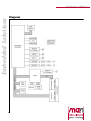
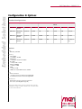
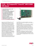
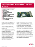
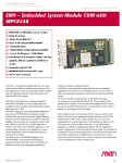
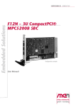
EM1 Data Sheet - 2008-07-31
Embedded Solutions
EM1 - Embedded System Module
with MPC5200
n
Embedded System Module with:
n
MPC5200 / 384 MHz
FPGA 12,000 LEs (approx.144,000 gates)
Up to 256 MB on-board DDR SDRAM
Up to 8 MB boot Flash, NAND Flash
2 MB SRAM, 16 MB additional SDRAM
Fast Ethernet, COM, USB 1.1 (front)
Dual CAN controller
MENMON™ BIOS for PowerPC® cards
COMs, graphics, IDE etc. optional via FPGA
Stackable with PCI-104
n
n
n
n
n
n
n
n
n
The EM1 can be supplied as a stand-alone module, with
an application-specific carrier card and/or with
additionally plugged PCI-104 modules.
The EM1 is controlled by the MPC5200 PowerPC®
processor which was specially developed for automotive
applications and which operates at up to 400 MHz and
700 MIPS. The complete ESM™ module in standard form
has an operational temperature of -40 to +85°C. The
CPU consumes less than 1 W at 384 MHz. The EM1 is
equipped with up to 256 MB soldered SDRAM and up to 1
GB NAND Flash as well as with 16 MB additional SDRAM,
up to 8 MB boot Flash and 2 MB battery-backed SRAM.
The EM1 provides one Fast Ethernet interface (second
interface prepared through FPGA), one serial line and
USB 1.1 at its front panel. As an alternative to RJ45,
D-Sub connectors guarantee reliable functions also in
harsh environments. Two CAN controllers with V2.0A/B
CAN protocol are included in the MPC5200. The physical
CAN interfaces are accessible via SA-Adapters™.
Further UARTs and other additional I/O functions can
be realized in the on-board FPGA and accessed via a
carrier board. The functionality of the FPGA is
dynamically loaded by the application software.
The EM1 comes with MENMON™ support. This firmware/BIOS
can be used for bootstrapping operating systems (from
1
disk, Flash or network), for hardware testing, or for
debugging applications without running any operating
system.
The EM1 is designed to operate under harsh
environmental conditions including -40 to +85°C
operation temperature, shock, vibration, humidity. It
focuses on applications in transportation (railways),
automotive and avionics.
For a first evaluation of the functions of the EM1 it
is strongly recommended to use the EK6 ESM™ starter
kit. The kit consists of the standard CPU module, an
FPGA loaded with additional I/O functions, the carrier
card with I/O connectors, an external PSU, VGA and
RJ45 to D-Sub cables, and an adapter for mounting a
PCI-104 module.
ESM™ modules are complete computers which consist of
the hardware (CPU, chip set, memory, I/O) which is not
fixed to any application-specific function, and an
FPGA programmed in VHDL code for user-defined I/O.
ESM™ modules are based on PCI. They have two system
connectors: J1 has a fixed signal assignment, while J2
is variable depending on the final applicationspecific configuration of the ESM™ and the carrier
board. J2 also feeds the I/O signals of the functions
programmed in the FPGA to the carrier card.
®
EM1 Data Sheet - 2008-07-31
Embedded Solutions
Technical Data
CPU
n PowerPC®
o MPC5200
o Up to 400MHz
Front Connections
n One USB 1.1 (Series A)
n Two Ethernet (RJ45 or D-Sub)
n One RS232 UART COM1(RJ45 or D-Sub)
Memory
n 2x16KB L1 data and instruction cache integrated in MPC5200
n Up to 256MB SDRAM system memory
o Soldered
o DDR
o 64MHz memory bus frequency
n Up to 1GB soldered NAND Flash (and more), FPGA-controlled
n 16MB additional SDRAM, FPGA-controlled, e.g. for video
data and NAND Flash firmware
n Up to 8MB boot Flash
n 2MB battery-backed SRAM, or: 128KB non-volatile FRAM
n Serial EEPROM 8kbits for factory settings
FPGA
n Standard factory FPGA configuration:
o Main bus interface
o 16Z070_IDEDISK - IDE controller for NAND Flash
o 16Z043_SDRAM - Additional SDRAM controller (16MB; 1MB
used for graphics)
o 16Z023_IDENHS - IDE controller (PIO mode 0;
non-hot-swap)
o 16Z044_DISP - Display controller (800 x 600,
60Hz/70Hz, 6-bit RGB)
o 16Z031_SPI - SPI touch panel controller
o 16Z025_UART - UART controller (controls COM10..COM13)
o 16Z034_GPIO - GPIO controller (6 lines)
n The FPGA offers the possibility to add customized I/O
functionality. See FPGA.
Mass Storage
n Parallel IDE (PATA)
o One port for hard-disk drives
o Available via I/O connector
o FPGA-controlled
n Up to 1GB soldered ATA NAND Flash (and more),
FPGA-controlled
2
PCI Interface
n 32-bit, 32-MHz PCI interface at PCI-104 connector J1
n Compliant with PCI Specification 2.2
n Support of 4 external masters
Graphics
n Available via I/O connector
n FPGA-controlled
Miscellaneous
n Real-time clock
n Power supervision and watchdog
I/O
n USB
o One USB 1.1 port
o Series A connector at front panel
o OHCI implementation
o Data rates up to 12Mbits/s
n Ethernet
o One 10/100Base-T Ethernet channel
o Second Ethernet channel can be implemented through
update of FPGA
o Two RJ45 or one D-Sub connector at front panel
n One RS232 UART (COM1)
o RJ45 or D-Sub connector at front panel
o Data rates up to 115.2kbits/s
o 512-byte transmit/receive buffer
o Handshake lines: CTS, RTS
n CAN bus
o Two CAN bus channels
o 2.0 A/B CAN protocol
o Data rates up to 1 Mbit/s
o Connection via on-board connectors
o External transceivers using SA-Adapters™
n Further I/O depending on FPGA configuration
Electrical Specifications
n Supply voltage/power consumption:
o +5V (-2%/+5%), 10mA max., only for USB
o +3.3V (-2%/+5%), 1A typ.
n MTBF: 232,000h @ 40°C (derived from MIL-HDBK-217F)
Mechanical Specifications
n Dimensions: conforming to ESM™ specification (PCB: 149mm
x 71mm), Type I-S
n Weight: 90g (w/o heat sink)
Environmental Specifications
n Temperature range (operation):
o -40..+85°C
o Airspeed: min. 2 m/s
n Temperature range (storage): -40..+85°C
n Relative humidity (operation): max. 95% non-condensing
n Relative humidity (storage): max. 95% non-condensing
n Altitude: -300m to + 3,000m
n Shock: 15g/11ms
n Bump: 10g/16ms
n Vibration (sinusoidal): 2g/10..150Hz
n Conformal coating on request
®
EM1 Data Sheet - 2008-07-31
Embedded Solutions
Technical Data
Safety
n PCB manufactured with a flammability rating of 94V-0 by
UL recognized manufacturers
EMC
n Tested according to EN 55022 (radio disturbance),
IEC1000-4-2 (ESD) and IEC1000-4-4 (burst)
BIOS
n MENMON™
Software Support
n VxWorks®
n Linux (ELinOS)
n QNX®
n PikeOS (partitionable RTOS) certified platform
n CANopen firmware (Vector Informatik)
n CAN support: MEN Driver Interface System (MDIS™ for
Windows®, Linux, VxWorks®, QNX®, OS-9®)
n For more information on supported operating system
versions and drivers see Software.
3
®
EM1 Data Sheet - 2008-07-31
Embedded Solutions
Diagram
4
®
EM1 Data Sheet - 2008-07-31
Embedded Solutions
Configuration & Options
Standard Configurations
Article No.
CPU Type
FPGA
System RAM
NAND Flash
Boot Flash
Additional
SRAM
Misc.
SDRAM
15EM01-00
MPC5200,
384MHz
12,000 LE
128 MB
128 MB
2 MB
16 MB
2 MB
Front I/O
15EM01N00
MPC5200B,
384MHz
18,752 LE
256 MB
1 GB
2 MB
16 MB
2 MB
Front I/O
15EM01A00
MPC5200B,
384MHz
18,752 LE
256 MB
128 MB
2 MB
16 MB
2 MB
Rear I/O
15EM01A01
MPC5200B,
384MHz
18,752 LE
256 MB
128 MB
2 MB
16 MB
2 MB
Rear I/O, 5V
only
Options
CPU
n MPC5200, 384 MHz
Memory
n System RAM
o 128 MB or 256 MB
n NAND Flash
o 0 MB up to maximum available
n Boot Flash
o 2 MB, 4 MB or 8 MB
n Additional SDRAM
o 0 MB or 16 MB
n SRAM
o 0 MB or 2 MB
n 128KB non-volatile FRAM instead of SRAM
I/O
n Front connections
o D-Sub connectors for Ethernet and COM/USB
n Second Ethernet channel at front through FPGA
Mechanical
n PCI and I/O connectors can also be placed for
face-to-face assembly (ESM™ Type N)
Please note that some of these options may only be
available for large volumes. Please ask our sales staff
for more information.
5
®
EM1 Data Sheet - 2008-07-31
Embedded Solutions
FPGA
FPGA Capabilities
n FPGA Altera® Cyclone™ EP1C12
o 12,060 logic elements
o 239,616 total RAM bits
n Connection
o Available pin count: 77 pins
o Functions available e.g. via I/O connector
Flexible Configuration
n This MEN board offers the possibility to add customized
I/O functionality in FPGA.
n It depends on the board type, pin counts and number of
logic elements which IP cores make sense and/or can be
implemented. Please contact MEN for information on
feasibility.
n Depending on the hardware platform, SA-Adapters™ can be
used to realize the physical lines.
MEN IP Cores
n MEN has a large number of standard IP cores to choose
from.
n Examples:
o IDE (e.g. PIO mode 0, UDMA mode 5)
o UARTs
o CAN bus
o Display control
o Fast Ethernet (10/100Base-T)
o ...
n For IP cores developed by MEN please refer to our IP core
overview.
o IP Core compare chart (PDF)
n MEN also offers development of new (customized) IP cores.
Third-Party IP Cores
n Third-party IP cores can also be used in combination with
MEN IP cores.
n Examples:
o www.altera.com
o www.opencores.org
FPGA Design Environment
n Altera® offers free download of Quartus® II Web Edition
o Complete environment for FPGA and CPLD design
o Includes schematic- and text-based design entry
o Integrated VHDL and Verilog HDL synthesis and support
for third-party synthesis software
o SOPC Builder system generation software
o Place-and-route, verification, and programming
n Altera® Quartus® II Web Edition FPGA design tool
6
®
EM1 Data Sheet - 2008-07-31
Embedded Solutions
Ordering Information
Related Hardware
Software: Windows
08EK06-00
13Z044-70
15EM01A00
15EM01A01
15EM01N00
ESM™ evaluation kit for EM1: Mini ATX
carrier board, EM1 with PowerPC® MPC5200 /
384MHz, 128MB DDR SDRAM, 128MB NAND Flash,
2MB SRAM, 16MB graphics memory, 2 MB boot
Flash, 1 Fast Ethernet, 1 UART, 1 USB 1.1,
graphics, IDE, RJ45 to D-Sub cable,VGA
cable, external PSU and adapter for
mounting of one PCI-104 module, 0..+60°C,
discontinued as of June 28, 2007
MPC5200B/384MHz, FPGA 18,752 logic
elements, 256MB SDRAM, 128MB NAND Flash,
2MB SRAM, 16MB graphics memory, 2MB boot
Flash, -40..+85°C with qualified components
MPC5200B/384MHz, FPGA 18,752 logic
elements, 256MB SDRAM, 128MB NAND Flash,
2MB SRAM, 16MB graphics memory, 2MB boot
Flash, single 5V supply, -40..+85°C with
qualified components
MPC5200B/384MHz, FPGA 18,752 logic
elements, 256 MB SDRAM, 1 GB NAND Flash, 2
MB SRAM, 16 MB graphics memory, 2 MB boot
Flash, front: 2 Fast Ethernet (RJ45), 1
UART (RJ45), 1 USB, -40..+85°C with
qualified components (also for ESM™
evaluation kit EK6N)
Windows® native driver (MEN) for
16Z044_DISP (frame buffer)
Software: VxWorks
10EM01-60
VxWorks® BSP (MEN) for EM1, EM1A, EM1N,
EK6, EK6N, F12N and F12
13Z025-60
VxWorks® native driver (MEN) for
16Z025_UART, 16Z057_UART and 16Z125_UART
Software: QNX
10EM01-40
QNX® BSP (MEN) for EM1, EM1A, EM1N, EK6,
EK6N, F12N and F12
13Z025-40
QNX® native driver (MEN) for 16Z025_UART
and 16Z125_UART
13Z044-40
QNX® native driver (MEN) for 16Z044_DISP
(frame buffer)
Software: Firmware/BIOS
14EM01-00
MENMON™ (Firmware) for EM1, EM1A, EM1N, F12
and F12N (object code)
Documentation
Miscellaneous
20EM00-00
ESM™ Specification
05F006-00
20EM01-00
EM1 User Manual
20EM01-ER
EM1 Errata
21APPN009
Application Note: 16Z025_UART and
16Z125_UART under Linux
21MENM-00
MENMON™ 2nd Edition User Manual
22Z025-ER
16Z025_UART Errata
RS232 interface cable RJ45 to 9-pin D-Sub
(1 COM to 1 COM), 2m
Software: OS independent
13Z015-06
MDIS4™/2004 driver (MEN) for 16Z029_CAN
(MSCAN/Layer2)
13Z016-06
MDIS4™/2004 driver (MEN) for 16Z029_CAN
(CANopen master)
13Z017-06
MDIS4™/2004 low-level driver sources (MEN)
for 16Z034_GPIO and 16Z037_GPIO
For the most up-to-date ordering information and direct
links to other data sheets and downloads, see the EM1
online data sheet under » www.men.de.
Software: Linux
7
13Z025-90
Linux native driver (MEN) for 16Z025_UART,
16Z057_UART and 16Z125_UART
13Z044-90
Linux native driver (MEN) for 16Z044_DISP
(frame buffer)
®
EM1 Data Sheet - 2008-07-31
Embedded Solutions
Contact Information
Germany
MEN Mikro Elektronik GmbH
Neuwieder Straße 5-7
90411 Nuremberg
Phone +49-911-99 33 5-0
Fax +49-911-99 33 5-901
E-mail [email protected]
www.men.de
France
MEN Mikro Elektronik SA
18, rue René Cassin
ZA de la Châtelaine
74240 Gaillard
Phone +33 (0) 450-955-312
Fax +33 (0) 450-955-211
E-mail [email protected]
www.men-france.fr
USA
MEN Micro, Inc.
24 North Main Street
Ambler, PA 19002
Phone (215) 542-9575
Fax (215) 542-9577
E-mail [email protected]
www.menmicro.com
The date of issue stated in this data sheet refers to the Technical Data only. Changes in ordering information given herein do not affect the date of issue.
All brand or product names are trademarks or registered trademarks of their respective holders.
Information in this document has been carefully checked and is believed to be accurate as of the date of publication; however, no responsibility is assumed for
inaccuracies. MEN Mikro Elektronik accepts no liability for consequential or incidental damages arising from the use of its products and reserves the right to
make changes on the products herein without notice to improve reliability, function or design. MEN Mikro Elektronik does not assume any liability arising out of
the application or use of the products described in this document.
The products of MEN Mikro Elektronik are not suited for use in nuclear reactors or for application in medical appliances used for therapeutical purposes.
Application of MEN's products in such plants is only possible after the user has precisely specified the operation environment and after MEN Mikro Elektronik
has consequently adapted and released the product.
Copyright © 2008 MEN Mikro Elektronik GmbH. All rights reserved.
8
®