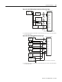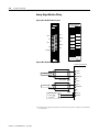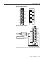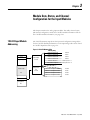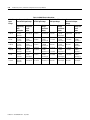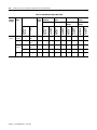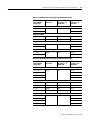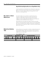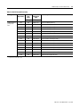
1
Compact I/O Analog
Modules
1769-IF4, -IF8, -OF2, -OF8C, and
-OF8V
User Manual
Important User Information
Solid state equipment has operational characteristics differing from those of
electromechanical equipment. Safety Guidelines for the Application, Installation and
Maintenance of Solid State Controls (Publication SGI-1.1 available from your local
Rockwell Automation sales office or online at http://www.ab.com/manuals/gi)
describes some important differences between solid state equipment and hard-wired
electromechanical devices. Because of this difference, and also because of the wide
variety of uses for solid state equipment, all persons responsible for applying this
equipment must satisfy themselves that each intended application of this equipment is
acceptable.
In no event will Rockwell Automation, Inc. be responsible or liable for indirect or
consequential damages resulting from the use or application of this equipment.
The examples and diagrams in this manual are included solely for illustrative purposes.
Because of the many variables and requirements associated with any particular
installation, Rockwell Automation, Inc. cannot assume responsibility or liability for
actual use based on the examples and diagrams.
No patent liability is assumed by Rockwell Automation, Inc. with respect to use of
information, circuits, equipment, or software described in this manual.
Reproduction of the contents of this manual, in whole or in part, without written
permission of Rockwell Automation, Inc. is prohibited.
Throughout this manual we use notes to make you aware of safety considerations.
WARNING
IMPORTANT
ATTENTION
Identifies information about practices or circumstances that can
cause an explosion in a hazardous environment, which may lead
to personal injury or death, property damage, or economic loss.
Identifies information that is critical for successful application
and understanding of the product.
Identifies information about practices or circumstances that can
lead to personal injury or death, property damage, or economic
loss. Attentions help you:
• identify a hazard
• avoid a hazard
• recognize the consequence
SHOCK HAZARD
Labels may be located on or inside the drive to alert people that
dangerous voltage may be present.
BURN HAZARD
Labels may be located on or inside the drive to alert people that
surfaces may be dangerous temperatures.
Summary of Changes
The 1769-IF8, -OF8C, and -OF8V modules have been added to this manual
since the last printing.
To help you find new and updated information in this release of the manual,
we have included change bars as shown next to this paragraph.
1
Publication 1769-UM002B-EN-P - July 2005
Summary of Changes
2
Notes:
Publication 1769-UM002B-EN-P - July 2005
Table of Contents
Preface
Who Should Use This Manual. . . . . . . . . . . . . . . . . . . . . . . . . .
How to Use This Manual. . . . . . . . . . . . . . . . . . . . . . . . . . . . . .
Manual Contents . . . . . . . . . . . . . . . . . . . . . . . . . . . . . . . . .
Related Documentation. . . . . . . . . . . . . . . . . . . . . . . . . . . .
Conventions Used in This Manual . . . . . . . . . . . . . . . . . . . . . .
Rockwell Automation Support . . . . . . . . . . . . . . . . . . . . . . . . .
Local Product Support . . . . . . . . . . . . . . . . . . . . . . . . . . . .
Technical Product Assistance . . . . . . . . . . . . . . . . . . . . . . .
Your Questions or Comments on the Manual . . . . . . . . . .
Preface-1
Preface-1
Preface-1
Preface-2
Preface-2
Preface-3
Preface-3
Preface-3
Preface-3
Chapter 1
Overview
How to Use Analog I/O . . . . . . . . . . . . . . . . . . . . . . . . . . . . . . . . . . . 1-1
General Description. . . . . . . . . . . . . . . . . . . . . . . . . . . . . . . . . . . . . . . 1-2
Hardware Features. . . . . . . . . . . . . . . . . . . . . . . . . . . . . . . . . . . . . 1-3
General Diagnostic Features . . . . . . . . . . . . . . . . . . . . . . . . . . . . . 1-5
System Overview . . . . . . . . . . . . . . . . . . . . . . . . . . . . . . . . . . . . . . . . . 1-5
System Operation. . . . . . . . . . . . . . . . . . . . . . . . . . . . . . . . . . . . . . 1-6
Module Operation . . . . . . . . . . . . . . . . . . . . . . . . . . . . . . . . . . . . . 1-7
Module Field Calibration. . . . . . . . . . . . . . . . . . . . . . . . . . . . . . . 1-10
Chapter 2
Installation and Wiring
i
Compliance to European Union Directives . . . . . . . . . . . . . . . . . . . . 2-1
EMC Directive. . . . . . . . . . . . . . . . . . . . . . . . . . . . . . . . . . . . . . . . 2-1
Low Voltage Directive. . . . . . . . . . . . . . . . . . . . . . . . . . . . . . . . . . 2-1
Power Requirements . . . . . . . . . . . . . . . . . . . . . . . . . . . . . . . . . . . . . . 2-2
General Considerations . . . . . . . . . . . . . . . . . . . . . . . . . . . . . . . . . . . . 2-2
Hazardous Location Considerations. . . . . . . . . . . . . . . . . . . . . . . 2-3
Prevent Electrostatic Discharge . . . . . . . . . . . . . . . . . . . . . . . . . . 2-3
Remove Power. . . . . . . . . . . . . . . . . . . . . . . . . . . . . . . . . . . . . . . . 2-4
Reducing Noise . . . . . . . . . . . . . . . . . . . . . . . . . . . . . . . . . . . . . . . 2-4
Protecting the Circuit Board from Contamination . . . . . . . . . . . 2-4
System Assembly . . . . . . . . . . . . . . . . . . . . . . . . . . . . . . . . . . . . . . . . . 2-4
Mounting . . . . . . . . . . . . . . . . . . . . . . . . . . . . . . . . . . . . . . . . . . . . . . . 2-6
Minimum Spacing . . . . . . . . . . . . . . . . . . . . . . . . . . . . . . . . . . . . . 2-6
Panel Mounting . . . . . . . . . . . . . . . . . . . . . . . . . . . . . . . . . . . . . . . 2-7
DIN Rail Mounting . . . . . . . . . . . . . . . . . . . . . . . . . . . . . . . . . . . . 2-8
Replacing a Single Module within a System . . . . . . . . . . . . . . . . . . . . 2-9
External Power Switch. . . . . . . . . . . . . . . . . . . . . . . . . . . . . . . . . . . . 2-10
Publication 1769-UM002B-EN-P - July 2005
Table of Contents
ii
Field Wiring Connections . . . . . . . . . . . . . . . . . . . . . . . . . . . . . . . . .
Grounding . . . . . . . . . . . . . . . . . . . . . . . . . . . . . . . . . . . . . . . . . .
System Wiring Guidelines . . . . . . . . . . . . . . . . . . . . . . . . . . . . . .
Labeling the Terminals . . . . . . . . . . . . . . . . . . . . . . . . . . . . . . . .
Removing the Finger-Safe Terminal Block . . . . . . . . . . . . . . . .
Wiring the Finger-Safe Terminal Block . . . . . . . . . . . . . . . . . . .
Wiring the Modules . . . . . . . . . . . . . . . . . . . . . . . . . . . . . . . . . . .
Terminal Door Label . . . . . . . . . . . . . . . . . . . . . . . . . . . . . . . . . .
Analog Input Modules Wiring. . . . . . . . . . . . . . . . . . . . . . . . . . .
Analog Output Modules Wiring . . . . . . . . . . . . . . . . . . . . . . . . .
2-10
2-10
2-11
2-15
2-15
2-16
2-17
2-18
2-19
2-24
Chapter 3
Module Data, Status, and Channel 1769-IF4 Input Module Addressing . . . . . . . . . . . . . . . . . . . . . . . . . . 3-1
1769-IF4 Input Image . . . . . . . . . . . . . . . . . . . . . . . . . . . . . . . . . . 3-2
Configuration for the Input
1769-IF4 Configuration File . . . . . . . . . . . . . . . . . . . . . . . . . . . . . 3-2
Modules
1769-IF4 Input Data File. . . . . . . . . . . . . . . . . . . . . . . . . . . . . . . . . . . 3-2
1769-IF4 Input Data Values . . . . . . . . . . . . . . . . . . . . . . . . . . . . . 3-3
1769-IF4 Configuration Data File . . . . . . . . . . . . . . . . . . . . . . . . . . . . 3-4
Channel Configuration . . . . . . . . . . . . . . . . . . . . . . . . . . . . . . . . . 3-5
Enable/Disable Channel . . . . . . . . . . . . . . . . . . . . . . . . . . . . . . . . 3-6
Input Filter Selection . . . . . . . . . . . . . . . . . . . . . . . . . . . . . . . . . . . 3-6
Input Type/Range Selection . . . . . . . . . . . . . . . . . . . . . . . . . . . . . 3-9
Input Data Selection Formats . . . . . . . . . . . . . . . . . . . . . . . . . . . 3-10
Effective Resolution . . . . . . . . . . . . . . . . . . . . . . . . . . . . . . . . . . 3-13
1769-IF8 Input Module Addressing . . . . . . . . . . . . . . . . . . . . . . . . . 3-16
1769-IF8 Input Image . . . . . . . . . . . . . . . . . . . . . . . . . . . . . . . . . 3-17
1769-IF8 Output Image. . . . . . . . . . . . . . . . . . . . . . . . . . . . . . . . 3-17
1769-IF8 Configuration File . . . . . . . . . . . . . . . . . . . . . . . . . . . . 3-17
1769-IF8 Input Data File. . . . . . . . . . . . . . . . . . . . . . . . . . . . . . . . . . 3-18
1769-IF8 Input Data Values . . . . . . . . . . . . . . . . . . . . . . . . . . . . 3-18
1769-IF8 Output Data File . . . . . . . . . . . . . . . . . . . . . . . . . . . . . . . . 3-20
1769-IF8 Configuration Data File . . . . . . . . . . . . . . . . . . . . . . . . . . . 3-20
Channel Configuration . . . . . . . . . . . . . . . . . . . . . . . . . . . . . . . . 3-22
Enable/Disable Channel . . . . . . . . . . . . . . . . . . . . . . . . . . . . . . . 3-23
Input Filter Selection . . . . . . . . . . . . . . . . . . . . . . . . . . . . . . . . . . 3-23
Input Type/Range Selection . . . . . . . . . . . . . . . . . . . . . . . . . . . . 3-27
Input Data Selection Formats . . . . . . . . . . . . . . . . . . . . . . . . . . . 3-27
1769-IF8 Real Time Sampling. . . . . . . . . . . . . . . . . . . . . . . . . . . 3-29
1769-IF8 Process Alarms . . . . . . . . . . . . . . . . . . . . . . . . . . . . . . 3-30
Publication 1769-UM002B-EN-P - July 2005
Table of Contents
iii
Chapter 4
Module Data, Status, and Channel 1769-OF2 Output Module Memory Map . . . . . . . . . . . . . . . . . . . . . . 4-1
1769-OF2 Output Data File . . . . . . . . . . . . . . . . . . . . . . . . . . . . . . . . 4-2
Configuration for the Output
1769-OF2 Input Data File . . . . . . . . . . . . . . . . . . . . . . . . . . . . . . . . . . 4-2
Modules
1769-OF2 Diagnostic Bits (D0 and D1). . . . . . . . . . . . . . . . . . . . 4-2
1769-OF2 Hold Last State Bits (H0 and H1). . . . . . . . . . . . . . . . 4-2
1769-OF2 Over-Range Flag Bits (O0 and O1) . . . . . . . . . . . . . . 4-3
1769-OF2 Under-Range Flag Bits (U0 and U1). . . . . . . . . . . . . . 4-3
1769-OF2 General Status Bits (S0 and S1). . . . . . . . . . . . . . . . . . 4-3
1769-OF2 Output Data Loopback/Echo . . . . . . . . . . . . . . . . . . 4-4
1769-OF2 Configuration Data File . . . . . . . . . . . . . . . . . . . . . . . . . . . 4-5
1769-OF2 Channel Configuration . . . . . . . . . . . . . . . . . . . . . . . . 4-6
1769-OF2 Enable/Disable Channel . . . . . . . . . . . . . . . . . . . . . . . 4-7
1769-OF2 Output Data Format Selection . . . . . . . . . . . . . . . . . . 4-7
1769-OF2 Output Type/Range Selection . . . . . . . . . . . . . . . . . . 4-8
1769-OF2 Fault Mode (FM0 and FM1) . . . . . . . . . . . . . . . . . . . . 4-8
1769-OF2 Program/Idle Mode (PM0 and PM1) . . . . . . . . . . . . . 4-9
1769-OF2 Program/Idle to Fault Enable (PFE0 and PFE1) . . 4-10
1769-OF2 Fault Value (Channel 0 and 1). . . . . . . . . . . . . . . . . . 4-11
1769-OF2 Program/Idle Value (Channel 0 and 1) . . . . . . . . . . 4-11
1769-OF2 Module Resolution . . . . . . . . . . . . . . . . . . . . . . . . . . . . . . 4-15
1769-OF8C Output Module Memory Map . . . . . . . . . . . . . . . . . . . 4-16
1769-OF8V Output Module Memory Map . . . . . . . . . . . . . . . . . . . 4-17
1769-OF8C and -OF8V Output Data File . . . . . . . . . . . . . . . . . . . . 4-18
Channel Alarm Unlatch . . . . . . . . . . . . . . . . . . . . . . . . . . . . . . . . 4-18
1769-OF8C and -OF8V Input Data File . . . . . . . . . . . . . . . . . . . . . 4-19
1769-OF8C and -OF8V Data Values . . . . . . . . . . . . . . . . . . . . . 4-19
1769-OF8C and -OF8V Output Data Loopback/Echo . . . . . . 4-21
1769-OF8C and -OF8V Configuration Data File . . . . . . . . . . . . . . 4-22
1769-OF8C and -OF8V Channel Configuration . . . . . . . . . . . . 4-24
1769-OF8C and -OF8V Enable/Disable Channel . . . . . . . . . . 4-25
Clamping/Limiting . . . . . . . . . . . . . . . . . . . . . . . . . . . . . . . . . . . 4-25
Clamp/Limit Alarms . . . . . . . . . . . . . . . . . . . . . . . . . . . . . . . . . . 4-26
Ramping . . . . . . . . . . . . . . . . . . . . . . . . . . . . . . . . . . . . . . . . . . . . 4-26
Hold for Initialization . . . . . . . . . . . . . . . . . . . . . . . . . . . . . . . . . 4-28
Open Wire Detection (1769-OF8C Only) . . . . . . . . . . . . . . . . . 4-29
1769-OF8C and -OF8V Fault Mode (FM). . . . . . . . . . . . . . . . . 4-29
1769-OF8C and -OF8V Program/Idle Mode (PM) . . . . . . . . . 4-30
1769-OF8C and -OF8V Program/Idle to Fault Enable (PFE). 4-31
1769-OF8C and -OF8V Fault Value . . . . . . . . . . . . . . . . . . . . . 4-31
1769-OF8C and -OF8V Program/Idle Value . . . . . . . . . . . . . . 4-32
Publication 1769-UM002B-EN-P - July 2005
Table of Contents
iv
Chapter 5
Module Diagnostics and
Troubleshooting
Safety Considerations. . . . . . . . . . . . . . . . . . . . . . . . . . . . . . . . . . . . . . 5-1
Indicator Lights . . . . . . . . . . . . . . . . . . . . . . . . . . . . . . . . . . . . . . . 5-1
Activating Devices When Troubleshooting . . . . . . . . . . . . . . . . . 5-1
Stand Clear of the Machine . . . . . . . . . . . . . . . . . . . . . . . . . . . . . . 5-2
Program Alteration . . . . . . . . . . . . . . . . . . . . . . . . . . . . . . . . . . . . 5-2
Safety Circuits. . . . . . . . . . . . . . . . . . . . . . . . . . . . . . . . . . . . . . . . . 5-2
Module Operation vs. Channel Operation . . . . . . . . . . . . . . . . . . . . . 5-2
Power-up Diagnostics . . . . . . . . . . . . . . . . . . . . . . . . . . . . . . . . . . . . . 5-3
Channel Diagnostics. . . . . . . . . . . . . . . . . . . . . . . . . . . . . . . . . . . . . . . 5-3
Out-of-Range Detection (Input and Output Modules) . . . . . . . . 5-3
Open-Circuit Detection (Input Modules Only) . . . . . . . . . . . . . . 5-3
Output Wire Broken/High Load Resistance
(Output Modules Only) . . . . . . . . . . . . . . . . . . . . . . . . . . . . . . . . . 5-4
Non-critical vs. Critical Module Errors. . . . . . . . . . . . . . . . . . . . . . . . 5-4
Module Error Definition Table . . . . . . . . . . . . . . . . . . . . . . . . . . . . . . 5-4
Module Error Field . . . . . . . . . . . . . . . . . . . . . . . . . . . . . . . . . . . . 5-5
Extended Error Information Field . . . . . . . . . . . . . . . . . . . . . . . . 5-5
Error Codes . . . . . . . . . . . . . . . . . . . . . . . . . . . . . . . . . . . . . . . . . . . . . 5-6
Module Inhibit Function . . . . . . . . . . . . . . . . . . . . . . . . . . . . . . . . . . 5-12
Contacting Rockwell Automation . . . . . . . . . . . . . . . . . . . . . . . . . . . 5-12
Appendix A
Specifications
General Specifications for 1769-IF4, -IF8, -OF2, -OF8C,
and -OF8V Modules . . . . . . . . . . . . . . . . . . . . . . . . . . . . . . . . . . . . . A-1
1769-IF4 Input Specifications . . . . . . . . . . . . . . . . . . . . . . . . . . . . . . A-3
1769-IF8 Input Specifications . . . . . . . . . . . . . . . . . . . . . . . . . . . . . . A-5
1769-OF2 Output Specifications. . . . . . . . . . . . . . . . . . . . . . . . . . . . A-7
1769-OF8C Output Specifications . . . . . . . . . . . . . . . . . . . . . . . . . . A-9
1769-OF8V Output Specifications . . . . . . . . . . . . . . . . . . . . . . . . . A-11
Appendix B
Module Addressing and
Configuration with MicroLogix
1500
Input Module Addressing . . . . . . . . . . . . . . . . . . . . . . . . . . . . . . . . . . B-1
Input Modules Input Image . . . . . . . . . . . . . . . . . . . . . . . . . . . . . B-2
Input Modules’ Configuration File . . . . . . . . . . . . . . . . . . . . . . . . B-3
Configuring Analog I/O Modules in a MicroLogix 1500 System . . . B-4
Configuring the Input Modules. . . . . . . . . . . . . . . . . . . . . . . . . . . B-6
Configuring the Output Modules . . . . . . . . . . . . . . . . . . . . . . . . . B-7
Appendix C
Configuration Using the RSLogix
5000 Generic Profile for
CompactLogix Controllers
Publication 1769-UM002B-EN-P - July 2005
Configuring I/O Modules . . . . . . . . . . . . . . . . . . . . . . . . . . . . . . . . . . C-6
Configuring Analog Output Modules. . . . . . . . . . . . . . . . . . . . . . C-7
Configuring Analog Input Modules . . . . . . . . . . . . . . . . . . . . . . . C-7
Table of Contents
v
Appendix D
Configuring Modules in a Remote
DeviceNet System with a
1769-ADN DeviceNet Adapter
Overview. . . . . . . . . . . . . . . . . . . . . . . . . . . . . . . . . . . . . . . . . . . . . . .
Add the DeviceNet Adapter to the Scanlist . . . . . . . . . . . . . . . . . . .
Configure the 1769-IF4 Input Module Example . . . . . . . . . . . . . . .
1769-IF4 Example of External Power . . . . . . . . . . . . . . . . . . . .
Configure the 1769-OF8C Output Module Example . . . . . . . . . . .
1769-OF8C Example of External Power . . . . . . . . . . . . . . . . . .
1769-OF8C Example of Output Channels. . . . . . . . . . . . . . . . .
D-1
D-2
D-4
D-6
D-7
D-8
D-9
Appendix E
Two’s Complement Binary
Numbers
Positive Decimal Values. . . . . . . . . . . . . . . . . . . . . . . . . . . . . . . . . . . . E-1
Negative Decimal Values . . . . . . . . . . . . . . . . . . . . . . . . . . . . . . . . . . . E-2
Glossary
Publication 1769-UM002B-EN-P - July 2005
Table of Contents
vi
Publication 1769-UM002B-EN-P - July 2005
Preface
Read this preface to familiarize yourself with the rest of the manual. This
preface covers the following topics:
•
•
•
•
•
who should use this manual
how to use this manual
related publications
conventions used in this manual
Rockwell Automation support
Who Should Use This
Manual
Use this manual if you are responsible for designing, installing, programming,
or troubleshooting control systems that use Allen-Bradley Compact™ I/O.
How to Use This Manual
As much as possible, we organized this manual to explain, in a task-by-task
manner, how to install, configure, program, operate and troubleshoot a control
system using the 1769 analog I/O modules.
Manual Contents
If you want...
An overview of the analog input and output modules
Chapter 1
Installation and wiring guidelines
Chapter 2
Input module addressing, configuration and status information
Chapter 3
Output module addressing, configuration and status information
Chapter 4
Information on module diagnostics and troubleshooting
Chapter 5
Specifications for the input and output modules
Appendix A
Information on addressing and configuration using MicroLogix 1500 and
RSLogix 500
Appendix B
Information on configuring the module using CompactLogix and RSLogix
5000
Appendix C
Information on configuring the module using 1769-ADN DeviceNet
Adapter and RSNetWorx
Appendix D
Information on understanding two’s complement binary numbers
Appendix E
Definitions of terms used in this manual
1
See
Glossary
Publication 1769-UM002B-EN-P - July 2005
2
Related Documentation
The table below provides a listing of publications that contain important
information about MicroLogix 1500 systems.
For
Read this document
Document number
A user manual containing information on how to install, MicroLogix™ 1500 User Manual
use and program your MicroLogix 1500 controller.
1764-UM001
A user manual containing information on how to install, DeviceNet Adapter User Manual
and use your 1769-ADN DeviceNet Adapter.
1769-UM001
A user manual containing information on how to install, CompactLogix User Manual
use and program your CompactLogix controller.
1769-UM007
An overview of 1769 Compact Discrete I/O modules
1769 Compact Discrete Input/Output Modules Product
Data
1769-2.1
An overview of the MicroLogix 1500 System, including
1769 Compact I/O.
MicroLogix™ 1500 System Overview
1764-SO001
In-depth information on grounding and wiring
Allen-Bradley programmable controllers.
Allen-Bradley Programmable Controller Grounding and
Wiring Guidelines
1770-4.1
If you would like a manual, you can:
• download a free electronic version from the internet at
www.ab.com/literature
• purchase a printed manual by:
– contacting your local distributor or Rockwell Automation
representative
– calling 1.800.963.9548 (USA/Canada) or 001.330.725.1574 (Outside
USA/Canada)
Conventions Used in This
Manual
Publication 1769-UM002B-EN-P - July 2005
The following conventions are used throughout this manual:
•
•
•
•
Bulleted lists (like this one) provide information not procedural steps.
Numbered lists provide sequential steps or hierarchical information.
Italic type is used for emphasis.
Text in this font indicates words or phrases you should type.
3
Rockwell Automation
Support
Rockwell Automation offers support services worldwide, with over
75 Sales/Support Offices, 512 authorized distributors and 260 authorized
Systems Integrators located throughout the United States alone, plus Rockwell
Automation representatives in every major country in the world.
Local Product Support
Contact your local Rockwell Automation representative for:
•
•
•
•
sales and order support
product technical training
warranty support
support service agreement
Technical Product Assistance
If you need to contact Rockwell Automation for technical assistance, please
review the information in Chapter 5, Module Diagnostics and Troubleshooting first.
Then call your local Rockwell Automation representative.
Your Questions or Comments on the Manual
If you find a problem with this manual, please notify us. If you have any
suggestions for how this manual could be made more useful to you, please
contact us at the address below:
Rockwell Automation
Automation Control and Information Group
Technical Communication, Dept. A602V
P.O. Box 2086
Milwaukee, WI 53201-2086
Publication 1769-UM002B-EN-P - July 2005
4
Notes:
Publication 1769-UM002B-EN-P - July 2005
Chapter
1
Overview
This chapter explains how analog data is used, and describes the 1769-IF4 and
-IF8 analog input modules and the 1769-OF2, -OF8C, and -OF8V analog
output modules. Included is information about:
•
•
•
•
How to Use Analog I/O
the use of analog I/O
the modules’ hardware and diagnostic features
an overview of the 1769 analog input system operation
an overview of the 1769 analog output system operation
Analog refers to the representation of numerical quantities by the
measurement of continuous physical variables. Analog applications are present
in many forms. The following application shows a typical use of analog data.
In this application, the processor controls the amount of fluid in a holding
tank by adjusting the valve opening. The valve is initially open 100%. As the
fluid level in the tank approaches the preset point, the processor modifies the
output to close the valve 90%, 80%, and so on, continuously adjusting the
valve to maintain the fluid level.
Figure 1.1 Analog I/O Application Example
Analog output
wired to valve
Valve
Controller
Analog I/O
Module
Level Sensor
Analog input wired
to tank
1
Publication 1769-UM002B-EN-P - July 2005
1-2
Overview
General Description
The 1769-IF4 and -IF8 analog input modules convert and digitally store analog
data for retrieval by controllers, such as the CompactLogix™ or MicroLogix™
1500. The module supports connections from any combination of up to four
voltage or current analog sensors for the 1769-IF4 and up to eight for the
1769-IF8. The high-impedance input channels can be wired as either
single-ended or differential inputs.
The 1769-OF2 output module provides two single-ended analog output
channels, each individually configurable for voltage or current. The
1769-OF8C and -OF8V output modules each provide eight single-ended
analog output channels.
Both modules provide the following input/output types/ranges:
Table 1.1 Normal and Full Ranges
Normal Operating Input Range
Full Module Range
±10V dc
± 10.5V dc
1 to 5V dc
0.5 - 5.25V dc
0 to 5V dc
-0.5 - +5.25V dc
0 to 10V dc
-0.5 - +10.5V dc
0 to 20 mA
0 - 21 mA
4 to 20 mA
3.2 - 21 mA
The data can be configured on board each module as:
•
•
•
•
Publication 1769-UM002B-EN-P - July 2005
Engineering Units
Scaled-for-PID
Percent
Raw/Proportional Data
Overview
1-3
Hardware Features
The modules contain removable terminal blocks. The 1769-IF4 and -IF8
channels can be wired as either single-ended or differential inputs. The
1769-OF2, -OF8C, and -OF8V channels are single-ended only. Module
configuration is normally done via the controller’s programming software. In
addition, some controllers support configuration via the user program. In
either case, the module configuration is stored in the memory of the controller.
Refer to your controller’s user manual for more information.
Figure 1.2 1769-OF2, -OF8C, -OF8V and -IF4 Analog Module’s Hardware Features
1
2a
3
OK
Analog
DANGER
Do Not Remove RTB Under Power
Unless Area is Non-Hazardous
10a
I out 0 +
I out 1 +
10
ANLG
Com
ANLG
Com
I out 3 +
ANLG
Com
I out 4 +
ANLG
Com
I out 5 +
I out 6 +
10b
ANLG
Com
I out 2 +
I out 7 +
+24V dc
ANGL
Com
ANLG
Com
ANLG
Com
dc
NEUT
Ensure Adjacent
Bus Lever is Unlatched/Latched
Before/After
Removing/Inserting Module
4
1769-OF8C
8a
7a
7a
2b
OK
Analog
5a
5b
9
6
7b
7b
8b
Table 1.2 1769-OF2, -OF8C, -OF8V, and -IF4 Feature Descriptions
Item
Description
1
bus lever (with locking function)
2a
upper panel mounting tab
2b
lower panel mounting tab
3
module status LEDs
4
module door with terminal identification label
5a
movable bus connector with female pins
5b
stationary bus connector with male pins
6
nameplate label
7a
upper tongue-and-groove slots
7b
lower tongue-and-groove slots
8a
upper DIN rail latch
8b
lower DIN rail latch
9
write-on label for user identification tags
10
removable terminal block (RTB) with finger-safe cover
10a
RTB upper retaining screw
10b
RTB lower retaining screw
Publication 1769-UM002B-EN-P - July 2005
1-4
Overview
Figure 1.3 1769-IF8 Analog Module’s Hardware Features
2a
1
3
WARNING -Do Not
Remove RTB Unless
Area is Non-Hazardous
10a
IN 1
IN 3
IN 5
IN 7
10
10b
IN 9
IN 11
IN 13
IN 15
DC COM
IN 0
IN 2
IN 4
IN 6
DC COM
IN 8
IN 10
IN 12
IN 14
IN 16
IN 17
IN 18
IN 19
IN 20
IN 21
IN 22
IN 23
IN 25
DC COM
IN 27
IN 29
IN 31
DC COM
IN 24
IN 26
IN 28
IN 30
4
1769-IQ32
8a
7a
7a
2b
5a
9
5b
6
7b
7b
8b
30538-M
Table 1.3 1769-IF8 Feature Descriptions
Publication 1769-UM002B-EN-P - July 2005
Item
Description
1
bus lever (with locking function)
2a
upper panel mounting tab
2b
lower panel mounting tab
3
I/O diagnostic LEDs
4
module door with terminal identification label
5a
movable bus connector with female pins
5b
stationary bus connector with male pins
6
nameplate label
7a
upper tongue-and-groove slots
7b
lower tongue-and-groove slots
8a
upper DIN rail latch
8b
lower DIN rail latch
9
write-on label for user identification tags
10
removable terminal block (RTB) with finger-safe cover
10a
RTB upper retaining screw
10b
RTB lower retaining screw
Overview
1-5
General Diagnostic Features
The analog modules contain diagnostic features that can help you identify the
source of problems that may occur during power-up or during normal channel
operation. These power-up and channel diagnostics are explained in chapter 6,
Module Diagnostics and Troubleshooting.
The modules communicate to the controller through the bus interface. The
modules also receive 5 and 24V dc power through the bus interface. The
1769-IF4, -OF2, -OF8C, and -OF8V modules feature an external 24V dc
power switch, providing you with the option of using an external power
supply. See External Power Switch on page 2-10 for details.
You can install as many analog modules as your power supply can support.
However, the modules have a power supply distance rating of 8, which means
that they may not be located more than 8 modules away from the system
power supply.
1
2
3
End Cap
Compact I/O
1
Compact I/O
2
Compact I/O
System Power Supply
Compact I/O
3
Compact I/O
4
Compact I/O
Figure 1.4 Determine Power Supply Distance
CompactLogix Controller
or I/O Communication
Adapter
Power Supply Distance
Compact I/O
Compact I/O
End Cap
MicroLogix 1500 Controller
with Integrated System
Power Supply
Compact I/O
OR
Compact I/O
System Overview
1
2
3
4
Power Supply Distance
Publication 1769-UM002B-EN-P - July 2005
1-6
Overview
System Operation
At power-up, the module performs a check of its internal circuits, memory,
and basic functions. During this time, the module status LED remains off. If
no faults are found during power-up diagnostics, the module status LED is
turned on.
After power-up checks are complete, the module waits for valid channel
configuration data. If an invalid configuration is detected, the module
generates a configuration error. Once a channel is properly configured and
enabled, it begins the analog-to-digital or digital-to-analog conversion process.
Input Modules
Each time a channel is read by the input modules, that analog data value is
tested by the modules for an over-range or under-range condition. If such a
condition is detected, a unique bit is set in the channel status word. The
channel status word is described in 1769-IF4 Input Data File on page 3-2 and
1769-IF8 Input Data File on page 3-18.
The controller reads the two’s complement binary converted analog data from
the modules. This typically occurs at the end of the program scan or when
commanded by the control program. If the controller and the modules
determine that the bus data transfer was made without error, the data is used in
your control program.
Output Modules
The output modules monitor channels for over-range and under-range
conditions and also for broken output wires and high load resistance (in
current mode only). If such a condition is detected, a unique bit is set in the
channel status word. The channel status word is described in 1769-OF2
Output Data File on page 4-2 and 1769-OF8C and -OF8V Output Data File
on page 4-18.
The output module receives two’s complement binary values from the bus
master. This typically occurs at the end of the program scan or when
commanded by the control program. If the controller and the module
determine that the bus transfer was completed without error, the output
module converts the data to an analog output signal.
Publication 1769-UM002B-EN-P - July 2005
Overview
1-7
Module Operation
Input Module Block Diagram
The input module’s input circuitry consists of four differential analog inputs
multiplexed into a single analog-to-digital (A/D) converter. The
A/D converter reads the selected input signal and converts it to a digital value
which is presented to the controller. The multiplexer sequentially switches
each input channel to the module’s A/D converter.
Figure 1.5 1769-IF4 Block Diagram
Galvanic
Isolation
Input
VA2
VA1
VS1
CH0
TXD
Vin+
Multiplexer
AIN+
Iin+
A/D
MCU
ASIC
RXD
AIN-
Bus
V/IinCOM
Vref
VREF
A-GND
CH1
CH2
Channel Select
VA3
VA1
(same as above)
VA2
DC/DC
Power
Supply
VS1
VS2
CH3
VA3
dc Neutral
A-GND
S-GND
+24V dc
Publication 1769-UM002B-EN-P - July 2005
1-8
Overview
Figure 1.6 1769-IF8 Block Diagram
Vin +
CH0 Iin +
V/ICom
Vin +
CH1 Iin +
V/ICom
Vin +
CH2 Iin +
V/ICom
Vin +
CH3 Iin +
V/ICom
Vin +
CH4 Iin +
V/ICom
Vin +
CH5 Iin +
V/ICom
Vin +
CH6 Iin +
V/ICom
Vin +
CH7 Iin +
V/ICom
High
Impedance
Gain
AD
Converter
CN2
(Out)
Opto
Coupler
Opto
Coupler
Select
Opto
Coupler
ASIC
Vref
LED
CPU
High
Impedance
Gain
AD
Converter
+24V
+15V
+5V
DC/DC
converter
-15V
GND
Select
Publication 1769-UM002B-EN-P - July 2005
GND
EN0
A1
A0
EN1
EN1
31542-M
CN1
(In)
Overview
1-9
Output Module Block Diagram
The output module uses a digital-to-analog (D/A) converter to read the digital
output data from the controller and convert it to an analog output signal.
Figure 1.7 1769-OF2 Block Diagram
Galvanic
Isolation
Output
VS1
VA1
VA2
Analog Switch
CH0
TXD
Iout
Iout+
D/A
Iout
ASIC
MCU
Selec
A-GND
VA2
Refout
RXD
Latch
COM
Bus
Vout+
VA3
A-GND
CH1
Latch
Selec
VS1
DC/DC
VA1 Power Supply
VS2
VA2
(same as above)
VA3
A-GND
dc Neutral
S-GND
+24V dc
Figure 1.8 1769-OF8C and -OF8V Block Diagram
The following diagram shows only one of eight outputs. For each analog
output, only one of the sections shown in broken-line boxes is implemented.
The 1769-OF8C module uses only the Current Out section while the
1769-OF8V module uses only the Voltage Out section.
Curent Out
OC
Detect
+15V
Voltage Out
GND -15V
500VDC Isoleted
Power Supply
JP
+
-
18 pin Terminal Block
16 Bit
DAC
OPTOS
+5V
16 pin backplane connector
+24 VDC
ESD Limit
CFU
64K Flash/
2K RAM
ASIC
EXT 24VDC
GND
GND
Publication 1769-UM002B-EN-P - July 2005
1-10
Overview
Module Field Calibration
The 1769-IF4 and -IF8 input modules performs autocalibration when a
channel is initially enabled. In addition, if a channel is configured differently
than the previously scanned channel, an autocalibration cycle is run as part of
the reconfiguration process.
The 1769-OF2, -OF8C, and -OF8V output modules’s calibration is
guaranteed by its design. No field calibration is required.
Publication 1769-UM002B-EN-P - July 2005
Chapter
2
Installation and Wiring
This chapter tells you how to:
•
•
•
•
•
•
Compliance to European
Union Directives
determine the power requirements for the modules
avoid electrostatic damage
install the module
wire the module’s terminal block
wire input devices
wire output devices
This product is approved for installation within the European Union and EEA
regions. It has been designed and tested to meet the following directives.
EMC Directive
The analog modules are tested to meet Council Directive 89/336/EEC
Electromagnetic Compatibility (EMC) and the following standards, in whole
or in part, documented in a technical construction file:
• EN 50081-2
EMC – Generic Emission Standard, Part 2 - Industrial Environment
• EN 50082-2
EMC – Generic Immunity Standard, Part 2 - Industrial Environment
This product is intended for use in an industrial environment.
Low Voltage Directive
This product is tested to meet Council Directive 73/23/EEC Low Voltage, by
applying the safety requirements of EN 61131-2 Programmable Controllers,
Part 2 – Equipment Requirements and Tests.
For specific information required by EN61131-2, see the appropriate sections
in this publication, as well as the following Allen-Bradley publications:
• Industrial Automation, Wiring and Grounding Guidelines for Noise Immunity,
publication 1770-4.1
• Automation Systems Catalog, publication B113
1
Publication 1769-UM002B-EN-P - July 2005
2-2
Installation and Wiring
Power Requirements
The modules receive power through the bus interface from the +5V dc/+24V
dc system power supply. Some modules can also be supplied 24V dc power by
an external power supply connected to the module’s terminal block.
Table 2.1 Maximum Current Draw
Module
5V dc
1769-IF4 (Series A)
1769-IF4 (Series B)
Not applicable
120 mA
1769-IF8 (Series A)
1769-OF2 (Series A)
120 mA
General Considerations
Publication 1769-UM002B-EN-P - July 2005
Not applicable
120 mA(1)
1769-OF8C (Series A)
(1)
60 mA(1)
70 mA
1769-OF2 (Series B)
1769-OF8V (Series A)
24V dc
145 mA
160 mA(1)
125 mA(1)
If the optional 24V dc Class 2 power supply is used, the 24V dc current draw from the bus is 0 mA.
Compact I/O is suitable for use in an industrial environment when installed in
accordance with these instructions. Specifically, this equipment is intended for
use in clean, dry environments (Pollution degree 2(1)) and to circuits not
exceeding Over Voltage Category II(2) (IEC 60664-1).(3)
(1)
Pollution Degree 2 is an environment where, normally, only non-conductive pollution occurs except that
occasionally a temporary conductivity caused by condensation shall be expected.
(2)
Over Voltage Category II is the load level section of the electrical distribution system. At this level transient
voltages are controlled and do not exceed the impulse voltage capability of the product’s insulation.
(3)
Pollution Degree 2 and Over Voltage Category II are International Electrotechnical Commission (IEC)
designations.
Installation and Wiring
2-3
Hazardous Location Considerations
This equipment is suitable for use in Class I, Division 2, Groups A, B, C, D or
non-hazardous locations only. The following WARNING statement applies to
use in hazardous locations.
ATTENTION
EXPLOSION HAZARD
• Substitution of components may impair suitability for
Class I, Division 2.
• Do not replace components or disconnect equipment
unless power has been switched off or the area is
known to be non-hazardous.
• Do not connect or disconnect components unless
power has been switched off or the area is known to be
non-hazardous.
• This product must be installed in an enclosure.
• All wiring must comply with N.E.C. article 501-4(b).
Prevent Electrostatic Discharge
ATTENTION
Electrostatic discharge can damage integrated circuits or
semiconductors if you touch analog I/O module bus
connector pins or the terminal block on the input module.
Follow these guidelines when you handle the module:
•
•
•
•
•
•
Touch a grounded object to discharge static potential.
Wear an approved wrist-strap grounding device.
Do not touch the bus connector or connector pins.
Do not touch circuit components inside the module.
If available, use a static-safe work station.
When it is not in use, keep the module in its
static-shield box.
Publication 1769-UM002B-EN-P - July 2005
2-4
Installation and Wiring
Remove Power
ATTENTION
Remove power before removing or inserting this module.
When you remove or insert a module with power applied,
an electrical arc may occur. An electrical arc can cause
personal injury or property damage by:
• sending an erroneous signal to your system’s field
devices, causing unintended machine motion
• causing an explosion in a hazardous environment
• Electrical arcing causes excessive wear to contacts on
both the module and its mating connector and may lead
to premature failure.
Reducing Noise
Most applications require installation in an industrial enclosure to reduce the
effects of electrical interference. Analog inputs and outputs are highly
susceptible to electrical noise. Electrical noise coupled to the analog inputs will
reduce the performance (accuracy) of the module.
Group your modules to minimize adverse effects from radiated electrical noise
and heat. Consider the following conditions when selecting a location for the
analog module. Position the module:
• away from sources of electrical noise such as hard-contact switches,
relays, and AC motor drives
• away from modules which generate significant radiated heat, such as the
1769-IA16. Refer to the module’s heat dissipation specification.
In addition, route shielded, twisted-pair analog input and output wiring away
from any high voltage I/O wiring.
Protecting the Circuit Board from Contamination
The printed circuit boards of the analog modules must be protected from dirt,
oil, moisture, and other airborne contaminants. To protect these boards, the
system must be installed in an enclosure suitable for the environment. The
interior of the enclosure should be kept clean and the enclosure door should
be kept closed whenever possible.
System Assembly
Publication 1769-UM002B-EN-P - July 2005
The module can be attached to the controller or an adjacent I/O module before
or after mounting. For mounting instructions, see Panel Mounting Using the
Dimensional Template on page 2-7, or DIN Rail Mounting on page 2-8. To
Installation and Wiring
2-5
work with a system that is already mounted, see Replacing a Single Module
within a System on page 2-9.
Figure 2.1 Assemble the Compact I/O System
3
4
2
1
6
1
5
1. Disconnect power.
2. Check that the bus lever of the module to be installed is in the unlocked
(fully right) position.
3. Use the upper and lower tongue-and-groove slots (1) to secure the
modules together (or to a controller).
4. Move the module back along the tongue-and-groove slots until the bus
connectors (2) line up with each other.
5. Push the bus lever back slightly to clear the positioning tab (3). Use your
fingers or a small screwdriver.
Publication 1769-UM002B-EN-P - July 2005
2-6
Installation and Wiring
6. To allow communication between the controller and module, move the
bus lever fully to the left (4) until it clicks. Ensure it is locked firmly in
place.
ATTENTION
When attaching I/O modules, it is very important
that the bus connectors are securely locked together
to ensure proper electrical connection.
7. Attach an end cap terminator (5) to the last module in the system by
using the tongue-and-groove slots as before.
8. Lock the end cap bus terminator (6).
IMPORTANT
A 1769-ECR or 1769-ECL right or left end cap must be
used to terminate the end of the bus.
Mounting
ATTENTION
During panel or DIN rail mounting of all devices, be sure
that all debris (metal chips, wire strands, etc.) is kept from
falling into the module. Debris that falls into the module
could cause damage at power up.
Minimum Spacing
Maintain spacing from enclosure walls, wireways, adjacent equipment, etc.
Allow 50 mm (2 in.) of space on all sides for adequate ventilation.
Figure 2.2 Space Requirements
Bottom
Publication 1769-UM002B-EN-P - July 2005
End Cap
Compact I/O
Compact I/O
Compact I/O
Host Controller
Compact I/O
Side
Compact I/O
Top
Side
Installation and Wiring
2-7
Panel Mounting
Mount the module to a panel using two screws per module. Use M4 or #8
panhead screws. Mounting screws are required on every module.
Figure 2.3 Panel Mounting Using the Dimensional Template
For more than 2 modules: (number of modules-1) X 35 mm (1,38 in.).
Right End Cap
Compact I/O
Compact I/O
Compact I/O
122.6±0.2
(4.826±0.008)
Host Controller
132
(5.197)
28.5
(1.12)
35
(1.38)
Refer to host controller documentation for this dimension.
NOTE: All dimensions are in mm (inches).
Hole spacing tolerance: ±0.04 mm (0.016 in.).
Figure 2.4 Panel Mounting for the 1769-IF8 Using the Dimensional Template
NOTE: Overall hole spacing
tolerance: ±0.4 mm (0.016 in.)
Locate holes every 17.5 mm (0.689 in) to allow for a
mix of single-wide and one-and-a-half-wide modules
(e.g., 1769-OA16).
Host Controller
Spacing for single-wide modules 35 mm (1.378 in).
l Mounting
Spacing for one-and-a-half-wide
modules 52.5 mm (2.067 in).
Refer to host controller documentation for this dimension.
Publication 1769-UM002B-EN-P - July 2005
2-8
Installation and Wiring
Panel Mounting Procedure Using Modules as a Template
The following procedure allows you to use the assembled modules as a
template for drilling holes in the panel. If you have sophisticated panel
mounting equipment, you can use the dimensional template provided on
page 2-7. Due to module mounting hole tolerance, it is important to follow
these procedures:
1. On a clean work surface, assemble no more than three modules.
2. Using the assembled modules as a template, carefully mark the center of
all module-mounting holes on the panel.
3. Return the assembled modules to the clean work surface, including any
previously mounted modules.
4. Drill and tap the mounting holes for the recommended M4 or #8 screw.
5. Place the modules back on the panel, and check for proper hole
alignment.
6. Attach the modules to the panel using the mounting screws.
TIP
If mounting more modules, mount only the last one of this
group and put the others aside. This reduces remounting
time during drilling and tapping of the next group.
7. Repeat steps 1 to 6 for any remaining modules.
DIN Rail Mounting
The module can be mounted using the following DIN rails:
35 x 7.5 mm (EN 50 022 - 35 x 7.5) or 35 x 15 mm (EN 50 022 - 35 x 15).
Before mounting the module on a DIN rail, close the DIN rail latches. Press
the DIN rail mounting area of the module against the DIN rail. The latches
will momentarily open and lock into place.
Publication 1769-UM002B-EN-P - July 2005
Installation and Wiring
Replacing a Single Module
within a System
2-9
The module can be replaced while the system is mounted to a panel (or DIN
rail). Follow these steps in order:
1. Remove power. See important note on 2-4.
2. On the module to be removed, remove the upper and lower mounting
screws from the module (or open the DIN latches using a flat-blade or
phillips-style screwdriver).
3. Move the bus lever to the right to disconnect (unlock) the bus.
4. On the right-side adjacent module, move its bus lever to the right
(unlock) to disconnect it from the module to be removed.
5. Gently slide the disconnected module forward. If you feel excessive
resistance, check that the module has been disconnected from the bus,
and that both mounting screws have been removed (or DIN latches
opened).
TIP
It may be necessary to rock the module slightly from front
to back to remove it, or, in a panel-mounted system, to
loosen the screws of adjacent modules.
6. Before installing the replacement module, be sure that the bus lever on
the module to be installed and on the right-side adjacent module are in
the unlocked (fully right) position.
7. Slide the replacement module into the open slot.
8. Connect the modules together by locking (fully left) the bus levers on
the replacement module and the right-side adjacent module.
9. Replace the mounting screws (or snap the module onto the DIN rail).
Publication 1769-UM002B-EN-P - July 2005
2-10
Installation and Wiring
External Power Switch
The analog modules have an external 24V dc power switch which gives you
the option of using an external power supply. The switch is located in on the
lower left portion of the module’s circuit board, as shown below. With the
switch pressed on the top (default), 24V dc power is drawn from the 1769
system power supply via the 1769 I/O bus. Pressed on the bottom, 24V dc
power is drawn from the external power supply.
Wire the external power supply to the module via the module’s terminal block.
The external power supply must be Class 2 rated, with a 24V dc range of 20.4
to 26.4V dc and a minimum current rating that meets the needs of the modules
used in your application. Refer to Maximum Current Draw on page 2-2.
IMPORTANT
Only 1769-IF4 and -OF2 Series B modules have the 24V
dc power switch.
Figure 2.5 External Power Switch
1769-IF4 and -OF2 Modules
External Power
Supply Switch
External Power Switch
Pressed on the Top
Bus Power (default)
BUS
EXT
Pressed on the Bottom
External Power
Bus Power (default)
External Power
Field Wiring Connections
1769-OF8C and -OF8V Modules
Grounding
This product is intended to be mounted to a well-grounded mounting surface
such as a metal panel. Additional grounding connections from the module’s
mounting tabs or DIN rail (if used) are not required unless the mounting
surface cannot be grounded. Refer to Industrial Automation Wiring and Grounding
Guidelines, Allen-Bradley publication 1770-4.1, for additional information.
Publication 1769-UM002B-EN-P - July 2005
Installation and Wiring
2-11
System Wiring Guidelines
Consider the following when wiring your system:
General
• All module commons (ANLG COM) are connected in the analog
module. The analog common (ANLG COM) is not connected to earth
ground inside the module.
• Channels are not isolated from each other.
• Do not use the analog module’s NC terminals as connection points.
• To ensure optimum accuracy, limit overall cable impedance by keeping
your cable as short as possible. Locate the I/O system as close to your
sensors or actuators as your application will permit.
• Use Belden™ 8761, or equivalent, shielded wire.
• Keep shield connection to ground as short as possible.
• Under normal conditions, the drain wire and shield junction must be
connected to earth ground via a panel or DIN rail mounting screw at
the analog I/O module end.(1)
1769-IF4 and -IF8 Input Modules
• If multiple power supplies are used with analog inputs, the power supply
commons must be connected together.
• The 1769-IF4 and -IF8 modules do not provide loop power for analog
inputs. Use a power supply that matches the input transmitter
specifications.
• Differential analog inputs are more immune to noise than single-ended
analog inputs.
• Voltages on Vin+, V/Iin-, and Iin+ of the 1769-IF4 and -IF8 modules
must be within ±10V dc of analog common.
1769-OF2, -OF8C, and -OF8V Output Modules
• Voltage outputs (Vout 0+ and Vout 1+ for 1769-OF2, Vout 0+
through Vout 7+ for 1769-OF8V) of the output modules are referenced
to ANLG COM. Load resistance for a voltage output channel must be
equal to or greater than 1K Ω.
• Current outputs (Iout 0+ and Iout 1+ for 1769-OF2, Iout 0+ through
Iout 7+ for 1769-OF8C) of the output modules source current that
returns to ANLG COM. Load resistance for a current output channel
must remain between 0 and 500 Ω.
(1)
In environments where high-frequency noise may be present, it may be necessary to directly ground cable
shields to earth at the module end and via a 0.1µF capacitor at the sensor end.
Publication 1769-UM002B-EN-P - July 2005
2-12
Installation and Wiring
Effect of Transducer/Sensor and Cable Length Impedance on Voltage Input
Accuracy
For voltage inputs, the length of the cable used between the transducer/sensor
and the 1769-IF4 or -IF8 module can affect the accuracy of the data provided
by the module.
Figure 2.6 Voltage Input Accuracy
Rs
Rc
+
Vs
V in
Ri
-
Rc
Where:
Rc = DC resistance of the cable (each conductor) depending on
cable length
Rs = Source impedance of analog transducer/sensor input
Ri = Impedance of the voltage input
(220 KΩ for 1769-IF4 and -IF8)
Vs = Voltage source
(voltage at the transducer/sensor input device)
Vin = Measured potential at the module input
%Ai = Percent added inaccuracy in a voltage-based system due
to source and cable impedance.
[ Ri × Vs ]
Vin = ------------------------------------------------------[ Rs + ( 2 × Rc ) + Ri ]
For example, for Belden 8761 two conductor, shielded cable:
Rc = 16 Ω/1000 ft
Rs = 0 (ideal
source)
Publication 1769-UM002B-EN-P - July 2005
Vin
% Ai = ⎛ 1 ∠ ---------⎞ × 100
⎝
Vs ⎠
Installation and Wiring
2-13
Table 2.2 Effect of Cable Length on Input Accuracy
Length of Cable (m)
dc resistance of the cable,
Rc (Ω)
Accuracy impact at the
input module
50
2.625
0.00238%
100
5.25
0.00477%
200
10.50
0.00954%
300
15.75
0.0143%
As input source impedance (Rs) and/or resistance (dc) of the cable (Rc) get
larger, system accuracy decreases. If you determine that the inaccuracy error is
significant, implementing the following equation in the control program can
compensate for the added inaccuracy error due to the impedance of the source
and cable.
[ Rs + ( 2 × Rc ) + Ri ]
Vs = Vin × ------------------------------------------------------Ri
In a current loop system, source and cable impedance do
not impact system accuracy.
TIP
Effect of Device and Cable Output Impedance on Output Module Accuracy
The maximum value of the output impedance is shown in the example below,
because it creates the largest deviation from an ideal voltage source.
Figure 2.7 Output Module Accuracy
Rs
Rc
+
Vs
V in
Ri
-
Rc
Where:
Rc = DC resistance of the cable (each conductor)
depending on cable length
Rs = Source impedance
(15 Ω for 1769-OF2 and 1 Ω for 1769-OF8V)
Ri = Impedance of the voltage input
(220 KΩ for 1769-IF4)
Vs = Voltage at the output of 1769-OF2
Vin = Measured potential at the module input
%Ai = Percent added inaccuracy in a voltage-based
system due to source and cable impedance.
[ Ri × Vs ]
Vin = ------------------------------------------------------[ Rs + ( 2 × Rc ) + Ri ]
Publication 1769-UM002B-EN-P - July 2005
2-14
Installation and Wiring
For example, for Belden 8761 two conductor, shielded cable and a 1769-IF4
input module:
Rc = 16 Ω/1000 ft
Rs = 15 Ω
Ri = 220 KΩ
Vin
% Ai = ⎛ 1 ∠ ---------⎞ × 100
⎝
Vs ⎠
Table 2.3 Effect of Output Impedance and Cable Length on Accuracy
Length of Cable (m)
dc resistance of the cable
Rc (Ω)
Accuracy impact at the
input module
50
2.625
0.00919%
100
5.25
0.01157%
200
10.50
0.01634%
300
15.75
0.02111%
As output impedance (Rs) and/or resistance (dc) of the cable (Rc) get larger,
system accuracy decreases. If you determine that the inaccuracy error is
significant, implementing the following equation in the control program can
compensate for the added inaccuracy error due to the impedance of the output
module and cable.
[ Rs + ( 2 × Rc ) + Ri ]
Vs = Vin × ------------------------------------------------------Ri
TIP
Publication 1769-UM002B-EN-P - July 2005
In a current loop system, source and cable impedance do
not impact system accuracy.
Installation and Wiring
2-15
Labeling the Terminals
A removable, write-on label is provided with the module. Remove the label
from the door, mark the identification of each terminal with permanent ink,
and slide the label back into the door. Your markings (ID tag) will be visible
when the module door is closed.
Figure 2.8 Terminal Labels
wiring the
finger-safe
terminal block
upper retaining screw
lower retaining screw
Removing the Finger-Safe Terminal Block
When wiring field devices to the module, it is not necessary to remove the
terminal block. If you remove the terminal block, use the write-on label on the
side of the terminal block to identify the module slot location and type. RTB
position can be indicated by circling either the ‘R’ for right side or ‘L’ for left
side.
Figure 2.9 Finger-Safe Terminal Block
SLOT # _____
MODULE TYPE ______
To remove the terminal block, loosen the upper and lower retaining screws.
The terminal block will back away from the module as you remove the screws.
When replacing the terminal block, torque the retaining screws to 0.46 Nm
(4.1 in-lbs).
Publication 1769-UM002B-EN-P - July 2005
2-16
Installation and Wiring
Wiring the Finger-Safe Terminal Block
When wiring the terminal block, keep the finger-safe cover in place.
1. Loosen the terminal screws to be wired.
2. Begin wiring at the bottom of the terminal block and move up.
3. Route the wire under the terminal pressure plate. You can use the bare
wire or a spade lug. The terminals accept a 6.35 mm (0.25 in.) spade lug.
TIP
The terminal screws are non-captive. Therefore, it is
possible to use a ring lug [maximum 1/4 inch o.d. with a
0.139 inch minimum i.d. (M3.5)] with the module.
4. Tighten the terminal screw making sure the pressure plate secures the
wire. Recommended torque when tightening terminal screws is 0.68 Nm
(6 in-lbs).
TIP
If you need to remove the finger-safe cover, insert a
screwdriver into one of the square, wiring holes and gently
pry the cover off. If you wire the terminal block with the
finger-safe cover removed, you will not be able to put it
back on the terminal block because the wires will be in the
way.
Wire Size and Terminal Screw Torque
Each terminal accepts up to two wires.
Table 2.4 Terminal Wire Considerations
Wire Type
Wire Size
Terminal Screw
Torque
Retaining Screw
Torque
Cu-90°C (194°F)
#14 to #22 AWG
0.68 Nm (6 in-lbs)
0.46 Nm (4.1 in-lbs)
Stranded Cu-90°C (194°F)
#16 to #22 AWG
0.68 Nm (6 in-lbs)
0.46 Nm (4.1 in-lbs)
Solid
Publication 1769-UM002B-EN-P - July 2005
Installation and Wiring
2-17
Wiring the Modules
ATTENTION
To prevent shock hazard, care should be taken when wiring
the module to analog signal sources. Before wiring any
analog module, disconnect power from the system power
supply and from any other source to the analog module.
After the analog module is properly installed, follow the wiring procedure
below. To ensure proper operation and high immunity to electrical noise,
always use Belden™ 8761 (shielded, twisted-pair) or equivalent wire.
ATTENTION
When wiring an analog input, take care to avoid connecting
a voltage source to a channel configured for current input.
Improper module operation or damage to the voltage
source can occur.
Never connect a voltage or current source to an analog
output channel.
Figure 2.10 Belden 8761 Wire
cable
Cut foil shield
and drain wire
signal wire
signal wire
drain wire
foil shield
signal wire
signal wire
Publication 1769-UM002B-EN-P - July 2005
2-18
Installation and Wiring
To wire your module follow these steps.
1. At each end of the cable, strip some casing to expose the individual
wires.
2. Trim the signal wires to 2-inch lengths. Strip about 3/16 inch (5 mm) of
insulation away to expose the end of the wire.
ATTENTION
Be careful when stripping wires. Wire fragments that
fall into a module could cause damage at power up.
3. At one end of the cable, twist the drain wire and foil shield together.
Under normal conditions, this drain wire and shield junction must be
connected to earth ground, via a panel or DIN rail mounting screw at
the analog I/O module end. Keep the length of the drain wire as short
as possible.
In environments where high frequency noise may be present, it may be
necessary to ground the cable shields to earth at the module end via a
0.1 µF capacitor at the sensor end for analog inputs and at the load end
for analog outputs.
4. At the other end of the cable, cut the drain wire and foil shield back to
the cable.
5. Connect the signal wires to the terminal block as shown in Analog Input
Modules Wiring on page 2-19 and Analog Output Modules Wiring on
page 2-24. Connect the other end of the cable to the analog input or
output device.
6. Repeat steps 1 through 5 for each channel on the module.
Terminal Door Label
A removable, write-on label is provided with the module. Remove the label
from the door, mark the identification of each terminal with permanent ink,
and slide the label back into the door. Your markings (ID tag) will be visible
when the module door is closed.
Publication 1769-UM002B-EN-P - July 2005
Installation and Wiring
2-19
Analog Input Modules Wiring
Figure 2.11 1769-IF4 Terminal Layout
DANGER
Do Not Remove RTB Under Power
Unless Area is Non-Hazardous.
V in 0 +
V/I in 0 -
I in 0 +
ANLG Com
V in 1 +
V/I in 1 -
I in 1 +
ANLG Com
V in 2 +
V/I in 2 -
I in 2 +
ANLG Com
V in 3 +
V/I in 3 -
I in 3 +
ANLG Com
+24V dc
dc NEUT
V in 0 +
V/I in 0 ANLG
Com
V/I in 1 -
I in 0+
V in 1 +
I in 1+
ANLG
Com
V in 2 +
V/I in 2 -
I in 2+
ANLG
Com
V/I in 3 -
V in 3 +
I in 3+
ANLG
Com
dc NEUT
+24V dc
Ensure Adjacent Bus Lever is
Unlatched/Latched Before/After
Removing/Inserting Module
1769-IF4
Figure 2.12 1769-IF4 Wiring Diagram Showing Differential Inputs
Belden 8761 cable (or equivalent)
1769-IF4
V/I in 0 ANLG Com
V/I in 1 ANLG Com
V/I in 2 ANLG Com
V/I in 3 ANLG Com
dc NEUT
–
Analog
Source
V in 0 +
+
I in 0+
V in 1 +
I in 1+
V in 2 +
earth ground
shield locally at
the module
I in 2+
V in 3 +
I in 3+
+24V dc
+ External 24V dc
Power Supply(1)
(2)
- (optional)
(1) The external power supply must be rated Class 2, with a 24V dc range of 20.4 to 26.4V dc and 60 mA minimum
for a single input module.
(2 ) Series B and later modules provide this option.
Publication 1769-UM002B-EN-P - July 2005
2-20
Installation and Wiring
Figure 2.13 1769-IF4 Wiring Single-ended Sensor/Transmitter Types
1769-IF4 Terminal Block
Sensor/
Transmitter
Supply
+
-
Current
Transmitter
+
Signal
Voltage
Transmitter
+
Ground
Signal
V in 0 +
V/I in 0 I in 0 +
ANLG Com
V in 1 +
V/I in 1 I in 1 +
ANLG Com
V in 2 +
V/I in 2 -
+
Voltage
Transmitter
Ground Signal
I in 2 +
ANLG Com
V in 3 +
V/I in 3 I in 3 +
ANLG Com
+24V dc
dc NEUT
External 24V dc
Power Supply(1)
(optional)(2)
+
-
(1) The external power supply must be rated Class 2, with a 24V dc range of 20.4 to 26.4V dc and 60 mA minimum
for a single input module.
(2 ) Series B and later modules provide this option.
Publication 1769-UM002B-EN-P - July 2005
Installation and Wiring
2-21
Figure 2.14 1769-IF4 Wiring Mixed Transmitter Types
Supply
Signal
V/I in 1 -
–
I in 1 +
ANLG Com
+
Differential
Current
Transmitter
Supply
I in 0 +
ANLG Com
V in 1 +
+
Differential
Voltage
Transmitter
–
V in 0 +
V/I in 0 -
+
–
–
1769-IF4 Terminal Block
Signal
Single-ended
Voltage
Transmitter
–
V in 2 +
V/I in 2 -
+
I in 2 +
ANLG Com
Signal
V in 3 +
+
V/I in 3 I in 3 +
2-Wire Current
Transmitter
Sensor/Transmi
tter Supply
ANLG Com
+24V dc
dc NEUT
+ Signal
+
–
External 24V dc
Power Supply
(optional)(1)
+
–
(1) The external power supply must be rated Class 2, with a 24V dc range of 20.4 to 26.4V dc and 60 mA minimum
for a single input module.
(2) Series B and later modules provide this option.
Publication 1769-UM002B-EN-P - July 2005
2-22
Installation and Wiring
Figure 2.15 1769-IF8 Terminal Layout
V in 0+
WARNING -Do Not
Remove RTB Unless
Area is Non-Hazardous
V in 4+
V/I in 4-
V/I in 0I in 0
I in 4
V in 1+
I in 0+
V in 5+
ANLG Com
V/I in 5-
V/I in 1I in 1
I in 5
V in 2+
I in 1+
V in 6+
ANLG Com
V/I in 6-
V/I in 2I in 2
I in 6
V in 7+
ANLG Com
I in 7
V/I in 3-
NC
ANLG Com
V/I in 7I in 3
NC
NC
NC
ANLG Com
V in 4+
I in 4+
V in 5+
V/I in 5ANLG Com
V/I in 6-
I in 5+
V in 6+
I in 6+
ANLG Com
V in 3+
I in 3+
ANLG Com
ANLG Com
V/I in 4-
I in 2+
V in 3+
V/I in 3-
V in 2+
V/I in 2-
ANLG Com
ANLG Com
V in 1+
V/I in 1-
ANLG Com
ANLG Com
V in 0+
V/I in 0-
ANLG Com
ANLG Com
NC
NC
V/I in 7ANLG Com
NC
V in 7+
I in 7+
NC
1769-IF8
Figure 2.16 1769-IF8 Wiring Differential Inputs
Belden 8761 cable (or equivalent)
analog source
–
V/I in 0ANLG Com
V/I in 1ANLG Com
V/I in 2ANLG Com
V/I in 3ANLG Com
NC
Publication 1769-UM002B-EN-P - July 2005
V in 0+
+
I in 0+
V in 2+
I in 2+
V in 3+
I in 3+
NC
V/I in 4ANLG Com
V in 1+
I in 1+
–
V/I in 5-
earth ground the
shield locally at
the module
ANLG Com
V/I in 6ANLG Com
V/I in 7ANLG Com
NC
V in 4+
I in 4+
V in 5+
I in 5+
V in 6+
I in 6+
V in 7+
I in 7+
NC
+
Installation and Wiring
2-23
Figure 2.17 1769-IF8 Wiring Single-Ended Sensor/Transmitter Types
1769-IF8 Terminal Block
Sensor/Tran +
smitter
Supply(1)
V in 0 +
Current
Transmitter
+ Signal
V/I in 0 I in 0 +
ANLG Com
V in 1 +
V/I in 1 -
Voltage
Transmitter
+ Ground
I in 1 +
ANLG Com
Signal
V in 2 +
V/I in 2 I in 2 +
ANLG Com
Voltage
Transmitter
+ Ground
Signal
V in 3 +
V/I in 3 I in 3 +
ANLG Com
NC
NC
Wiring for channels 4-7 are identical.
(1) The external power supply must be rated Class 2, with a 24V dc range of 20.4 to 26.4V dc and 60 mA minimum
for a single input module.
Figure 2.18 1769-IF8 Wiring Mixed Transmitter Types
Single-ended
Voltage
Transmitter(1)
–
Signal
V in 0 +
V/I in 0 -
+
Differential
Voltage
Transmitter
– Supply +
1769-IF8 Terminal Block
+Signal
–
Differential –
Signal
Current
+
Transmitter
– Supply +
I in 0 +
ANLG Com
V in 1 +
V/I in 1 I in 1 +
ANLG Com
V in 2 +
V/I in 2 I in 2 +
ANLG Com
V in 3 +
V/I in 3 I in 3 +
2-Wire
Current
Transmitter
Sensor/
Transmitter
Supply
Signal
+
ANLG Com
NC
NC
+
–
Wiring for channels 4-7 are identical.
(1) The external power supply must be rated Class 2, with a 24V dc range of 20.4 to 26.4V dc and 60 mA minimum
for a single input module.
Publication 1769-UM002B-EN-P - July 2005
2-24
Installation and Wiring
Analog Output Modules Wiring
Figure 2.19 1769-OF2 Terminal Layout
DANGER
Do Not Remove RTB Under Power
Unless Area is Non-Hazardous.
V in 0 ANLG
Com 0
I out 0 +
NC
I out 1 +
V out 0 +
ANLG Com
V out 1 +
ANLG Com
NC
+24V dc
dc Neutral
I out 0 +
NC
I out 1 +
NC
dc NEUT
ANLG
Com 3
NC
V in 0 +
I in 0
V out 0 +
ANLG Com
V out 1 +
ANLG Com
+24V dc
I in 3
NC
Ensure Adjacent Bus Lever is
Unlatched/Latched Before/After
Removing/Inserting Module
1769-OF2
Figure 2.20 1769-OF2 Wiring Diagram
1769-OF2 Terminal Block
V out 0 +
I out 0 +
Voltage Load
ANLG Com
earth ground
NC
V out 1 +
I out 1 +
Current Load
ANLG Com
NC
earth ground
External 24V dc +
Power Supply
(optional)(1)
+24V dc
dc NEUT
(1) The external power supply must be rated Class 2, with a 24V dc range of 20.4 to 26.4V dc and 120 mA minimum
per output module.
Publication 1769-UM002B-EN-P - July 2005
Installation and Wiring
2-25
Figure 2.21 1769-OF8C Terminal Layout
DANGER
Do Not Remove RTB Under Power
Unless Area is Non-Hazardous.
ANLG Com
I out 0+
ANLG Com
I out 1+
ANLG Com
I out 2+
ANLG Com
I out 3+
ANLG Com
I out 4+
ANLG Com
I out 5+
ANLG Com
I out 6+
ANLG Com
I out 7+
I out 1+
ANLG
Com
ANLG
Com
ANLG
Com
ANLG
Com
I out 0+
I out 2+
I out 3+
I out 4+
I out 5+
I out 6+
I out 7+
dc NEUT
+24V
dc
+24
v dc
ANLG
Com
ANLG
Com
ANLG
Com
ANLG
Com
dc NEUT
Ensure Adjacent Bus Lever is
Unlatched/Latched Before/After
Removing/Inserting Module
+24V dc
1769-OF8C
Figure 2.22 1769-OF8C Wiring Diagram
I out 0+
ANLG Com
ANLG Com
I out 1+
ANLG Com
I out 2+
ANLG Com
Current Load
I out 3+
ANLG Com
earth ground
External 24V dc Power +
Supply (optional)(1) -
I out 4+
ANLG Com
I out 5+
ANLG Com
I out 6+
ANLG Com
I out 7+
dc NEUT
+24V dc
(1) The external power supply must be rated Class 2, with a 24V dc range of 20.4 to 26.4V dc and 120 mA minimum
per output module.
Publication 1769-UM002B-EN-P - July 2005
2-26
Installation and Wiring
Figure 2.23 1769-OF8V Terminal Layout
DANGER
Do Not Remove RTB Under Power
Unless Area is Non-Hazardous.
ANLG Com
V out 0+
ANLG Com
V out 1+
ANLG Com
V out 2+
ANLG Com
V out 3+
ANLG Com
V out 4+
ANLG Com
V out 5+
ANLG Com
V out 6+
ANLG Com
V out 7+
V out 1+
ANLG
Com
ANLG
Com
ANLG
Com
ANLG
Com
V out 0+
V out 2+
V out 3+
V out 4+
V out 5+
V out 6+
V out 7+
dc NEUT
+24V
dc
+24
v dc
ANLG
Com
ANLG
Com
ANLG
Com
ANLG
Com
dc NEUT
Ensure Adjacent Bus Lever is
Unlatched/Latched Before/After
Removing/Inserting Module
+24V dc
1769-OF8V
Figure 2.24 1769-OF8V Wiring Diagram
V out 0+
ANLG Com
ANLG Com
V out 1+
ANLG Com
V out 2+
ANLG Com
Voltage Load
V out 3+
ANLG Com
earth ground
External 24V dc Power +
Supply (optional)(1) -
V out 4+
ANLG Com
V out 5+
ANLG Com
V out 6+
ANLG Com
V out 7+
dc NEUT
+24V dc
(1) The external power supply must be rated Class 2, with a 24V dc range of 20.4 to 26.4V dc and 120 mA minimum
per output module.
Publication 1769-UM002B-EN-P - July 2005
Chapter
3
Module Data, Status, and Channel
Configuration for the Input Modules
This chapter examines the analog input modules’ data table, channel status,
and channel configuration word. The 1769-IF4 module information follows.
For 1769-IF8 module information, see page 3-16.
1769-IF4 Input Module
Addressing
The 1769-IF4 memory map shows the input and configuration image tables
for the 1769-IF4. Detailed information on the input image table can be found
in 1769-IF4 Input Data File on page 3-2.
Figure 3.1 1769-IF4 Memory Map
slot e
Input Image
Output Image
File
Input Image
6 words
Configuration
File
4 words
Memory Map
Channel 0 Data Word
Channel 1 Data Word
Channel 2 Data Word
Word 0
Word 1
Channel 3 Data Word
General Status Bits
Over-/Under-range Bits
Word 3
Word 4, bits 0 to 3
Word 5, bits 0 to 15
Channel 0 Configuration Word
Channel 1 Configuration Word
Word 0
Word 1
Word 2
Word 3
Word 2
Channel 2 Configuration Word
Channel 3 Configuration Word
Bit 15
Bit 0
slot e
Configuration
File
1
Publication 1769-UM002B-EN-P - July 2005
3-2
Module Data, Status, and Channel Configuration for the Input Modules
1769-IF4 Input Image
The 1769-IF4 input image file represents data words and status bits. Input
words 0 through 3 hold the input data that represents the value of the analog
inputs for channels 0 through 3. These data words are valid only when the
channel is enabled and there are no errors. Input words 4 and 5 hold the status
bits. To receive valid status information, the channel must be enabled.
You can access information in the input image file using
the programming software configuration screen.
TIP
1769-IF4 Configuration File
The configuration file contains information that you use to define the way a
specific channel functions. The configuration file is explained in more detail in
1769-IF4 Configuration Data File on page 3-4.
Not all controllers support program access to the
configuration file. Refer to your controller’s user manual.
TIP
The input data table lets you access analog input module read data for use in
the control program, via word and bit access. The data table structure is shown
in table below.
1769-IF4 Input Data File
Table 3.1 1769-IF4 Input Data Table
Word/Bit
15
14
13
12
Word 0
SGN
Analog Input Data Value Channel 0
Word 1
SGN
Analog Input Data Value Channel 1
Word 2
SGN
Analog Input Data Value Channel 2
Word 3
SGN
Analog Input Data Value Channel 3
Word 4
Word 5
11
10
9
8
Not Used (Bits set to 0)
U0
Publication 1769-UM002B-EN-P - July 2005
O0
U1
O1
U2
O2
U3
O3
7
6
5
4
3
2
1
0
S3
S2
S1
S0
Set to zero
Module Data, Status, and Channel Configuration for the Input Modules
3-3
1769-IF4 Input Data Values
Words 0 through 3 contain the converted analog input data from the field
device. The most significant bit (MSB) is the sign bit.
General Status Bits (S0 through S3)
Word 4, bits 0 through 3 contain the general operational status bits for input
channels 0 through 3. If set (1), these bits indicate an error associated with that
channel. The over- and under-range bits for channels 0 through 3 are logically
ORed to the appropriate general status bit.
Over-Range Flag Bits (O0 through O3)
Over-range bits for channels 3 through 0 are contained in word 5, bits 8, 10,
12, and 14. They apply to all input types. When set (1), this bit indicates input
signals beyond the normal operating range. However, the module continues to
convert analog data to the maximum full range value. The bit is automatically
reset (0) by the module when the over-range condition is cleared and the data
value is within the normal operating range.
Under-Range Flag Bits (U0 through U3)
Under-range bits for channels 3 through 0 are contained in word 5, bits 9, 11,
13, and 15. They apply to all input types. When set (1), this bit indicates input
signals below the normal operating range. It may also indicate an open circuit
condition, when the module is configured for the 4 to 20 mA range. However,
the module continues to convert analog data to the minimum full range value.
The bit is automatically reset (0) by the module when the under-range
condition is cleared and the data value is within the normal operating range.
Publication 1769-UM002B-EN-P - July 2005
3-4
Module Data, Status, and Channel Configuration for the Input Modules
1769-IF4 Configuration Data
File
The configuration file lets you determine how each individual input channel
will operate. Parameters such as the input type and data format are set up using
this file. This data file is writable and readable. The default value of the
configuration data table is all zeros. The structure of the channel configuration
file is shown below.
Table 3.2 1769-IF4 Configuration Data Table(1)
Word/Bit
Word 0
Word 1
Word 2
Word 3
(1)
15
Enable Channel 0
Enable Channel 1
Enable Channel 2
Enable Channel 3
14
13
12
Input Data Format
Select Channel 0
Input Data Format
Select Channel 1
Input Data Format
Select Channel 2
Input Data Format
Select Channel 3
11
10
9
8
Input Type/Range
Select Channel 0
Input Type/Range
Select Channel 1
Input Type/Range
Select Channel 2
Input Type/Range
Select Channel 3
7
6
5
4
Reserved
Reserved
Reserved
Reserved
3
2
1
0
Input Filter Select
Channel 0
Input Filter Select
Channel 1
Input Filter Select
Channel 2
Input Filter Select
Channel 3
The ability to change these values using your control program is not supported by all controllers. Refer to your controller manual for details.
The configuration file is typically modified using the programming software
configuration screen. For information on configuring the module using
MicroLogix 1500 and RSLogix 500, see Appendix B; for CompactLogix and
RSLogix 5000, see Appendix C; for 1769-ADN DeviceNet Adapter and
RSNetWorx, see Appendix D.
The configuration file can also be modified through the control program, if
supported by the controller. The structure and bit settings are shown in
Channel Configuration on page 3-5.
Publication 1769-UM002B-EN-P - July 2005
Module Data, Status, and Channel Configuration for the Input Modules
3-5
Channel Configuration
Each channel configuration word consists of bit fields, the settings of which
determine how the channel operates. See the table below and the descriptions
that follow for valid configuration settings and their meanings. The default bit
status of the configuration file is all zeros.
Table 3.3 Bit Definitions for Channel Configuration Words 0 through 3
Bit(s)
0 to 3
Define
These bit settings
15
14
13
12
11
10
9
8
7 6 5 4
Input Filter Select
Indicate this
3
2
1
0
0
0
0
0
60 Hz
0
0
0
1
50 Hz
0
0
1
0
Not Used
0
0
1
1
250 Hz
0
1
0
0
500 Hz
Not Used(1)
4 to 7
8 to
11
Reserved
Reserved(2)
Input Type/Range
Select
0
0
0
0
-10 to +10V dc
0
0
0
1
0 to 5V dc
0
0
1
0
0 to 10V dc
0
0
1
1
0
1
0
0
1 to 5V dc
0
1
0
1
0 to 20 mA
Not Used
4 to 20 mA
Not Used1
12 to
14
Input Data
Format Select
0
0
0
Raw/Proportional Data
0
0
1
Engineering Units
0
1
0
Scaled for PID(3)
0
1
1
Percent Range
Not Used1
15
Enable Channel
1
Enabled
0
Disabled
(1)
Any attempt to write a non-valid (not used) bit configuration into any selection field results in a module configuration error. See Configuration Errors on page 5-6.
(2)
If reserved bits are not equal to zero, a configuration error occurs.
(3)
This range is applicable to the PID function of the MicroLogix 1500 packaged controller, PLC, or SLC controllers. Logix controllers can use this or one of the other ranges for
their PID functions.
Publication 1769-UM002B-EN-P - July 2005
3-6
Module Data, Status, and Channel Configuration for the Input Modules
Enable/Disable Channel
This configuration selection lets each channel to be individually enabled.
TIP
When a channel is not enabled (0), no voltage or current
input is provided to the controller by the A/D converter.
Input Filter Selection
The input filter selection field lets you select the filter frequency for each
channel and provides system status of the input filter setting for analog input
channels 0 through 3. The filter frequency affects the noise rejection
characteristics, as explained below. Select a filter frequency considering
acceptable noise and step response time.
Noise Rejection
The 1769-IF4 uses a digital filter that provides noise rejection for the input
signals. The filter is programmable, allowing you to select from four filter
frequencies for each channel. The digital filter provides the highest noise
rejection at the selected filter frequency. A lower frequency (60 Hz versus 250
Hz) can provide better noise rejection but it increases channel update time.
Transducer power supply noise, transducer circuit noise, or process variable
irregularities may also be sources of normal mode noise.
Common Mode Rejection is better than 60 dB at 50 and 60 Hz, with the 50
and 60 Hz filters selected, respectively. The module performs well in the
presence of common mode noise as long as the signals applied to the user plus
and minus input terminals do not exceed the common mode voltage rating (±
10 V) of the module. Improper earth ground may be a source of common
mode noise.
Channel Step Response
The selected channel filter frequency determines the channel’s step response.
The step response is the time required for the analog input signal to reach
100% of its expected final value. This means that if an input signal changes
faster than the channel step response, a portion of that signal will be
attenuated by the channel filter.
Table 3.4 Filter Frequency and Step Response
Publication 1769-UM002B-EN-P - July 2005
Filter Frequency
Cut-off Frequency
Step Response
50 Hz
13.1 Hz
60 ms
60 Hz
15.7 Hz
50 ms
250 Hz
65.5 Hz
12 ms
500 Hz
131 Hz
6 ms
Module Data, Status, and Channel Configuration for the Input Modules
3-7
Channel Cut-Off Frequency
The -3 dB frequency is the filter cut-off frequency. The cut-off frequency is
defined as the point on the frequency response curve where frequency
components of the input signal are passed with 3 dB of attenuation. All input
frequency components at or below the cut-off frequency are passed by the
digital filter with less than 3 dB of attenuation. All frequency components
above the cut-off frequency are increasingly attenuated as shown in the graphs
below.
The cut-off frequency for each channel is defined by its filter frequency
selection. Choose a filter frequency so that your fastest changing signal is
below that of the filter’s cut-off frequency. The cut-off frequency should not
be confused with the update time. The cut-off frequency relates to how the
digital filter attenuates frequency components of the input signal. The update
time defines the rate at which an input channel is scanned and its channel data
word is updated.
Figure 3.2 Frequency Response Graphs
50 Hz Input Filter Frequency
60 Hz Input Filter Frequency
0
–3 dB
–20
–20
–40
–40
–60
–60
Gain (dB)
Gain (dB)
0
–80
–100
–120
–80
–100
–120
–140
–140
–160
–160
–180
–180
–200
0
50
100
150
200
250
–200
300
Frequency (Hz)
13.1 Hz
–3 dB
0
250 Hz Input Filter Frequency
–20
–20
–40
–40
–60
–60
–80
–100
–120
–160
–180
–180
65.5 Hz
500
750
Frequency (Hz)
900
300
360
1150
1300
2500
3000
–3 dB
–120
–140
250
240
–80
–160
0
180
Frequency (Hz)
–100
–140
–200
120
500 Hz Input Filter Frequency
0
–3 dB
Gain (dB)
Gain (dB)
0
60
15.72 Hz
–200
0
131 Hz
500
1000
1500
2000
Frequency (Hz)
Publication 1769-UM002B-EN-P - July 2005
3-8
Module Data, Status, and Channel Configuration for the Input Modules
Module Update Time and Scanning Process
The module update time is defined as the time required for the module to
sample and convert the input signals of all enabled input channels and provide
the resulting data values to the processor. Module update time can be
calculated by adding the sum of all enabled channel times. Channel times
include channel scan time, channel switching time, and reconfiguration time.
The module sequentially samples the channels in a continuous loop.
Figure 3.3 Sequential Sampling
Channel 0 Disabled
Enabled
Sample
Channel 0
Channel 1 Disabled
Enabled
Sample
Channel 1
Channel 2 Disabled
Enabled
Sample
Channel 2
Channel 3 Disabled
Enabled
Sample
Channel 3
Table 3.5 shows the channel update times. The fastest module update time
occurs when only one channel is enabled with a 500 Hz filter (4 ms). If more
than one channel is enabled, the update time is faster if both channels have the
same configuration. See the first example on page 3-9. The slowest module
update time occurs when all four channels are enabled with different
configurations. See the second example on page 3-9.
Table 3.5 Channel Update Time
Filter Frequency
Channel Update Time
50 Hz
22 ms
60 Hz
19 ms
250 Hz
6 ms
500 Hz
4 ms
Channel Switching and Reconfiguration Times
The table below provides the channel switching and reconfiguration times for
a channel.
Table 3.6 Channel Switching and Reconfiguration Times
Description
Duration
50 Hz
60 Hz
250 Hz
500 Hz
Channel Switching
Time
The time it takes the module to switch from one channel to
another.
46 ms
39 ms
14 ms
10 ms
Channel-to-Channel
Reconfiguration Time
The time it takes the module to change its configuration settings
for a difference in configuration between one channel and another.
116 ms
96 ms
20 ms
8 ms
Publication 1769-UM002B-EN-P - July 2005
Module Data, Status, and Channel Configuration for the Input Modules
3-9
Examples of Calculating Module Update Time
EXAMPLE
1. Two Channels Enabled with Identical Configurations
The following example calculates the 1769-IF4 module update time for two channels enabled with
the same configuration and a 500 Hz filter.
Module Update Time = [Ch 0 Update Time + Ch 0 Switching Time] + [Ch 1 Update Time + Ch 1 Switching Time]
28 = [4 ms + 10 ms] + [4 ms + 10 ms]
EXAMPLE
2. Three Channels Enabled with Different Configurations
The following example calculates the module update time for three channels with the following
configurations:
• Channel 0: ±10V dc with 60 Hz filter
• Channel 1: ±10V dc with 500 Hz filter
• Channel 2: 4 to 20 mA with 250 Hz filter
Module Update Time =[Ch 0 Reconfiguration Time + Ch 0 Update Time + Ch 0 Switching Time]
+
[Ch 1 Reconfiguration Time + Ch 1 Update Time + Ch 1 Switching Time]
+
[Ch 2 Reconfiguration Time + Ch 2 Scan Time + Ch 2 Switching Time]
216 = [ 96 ms + 19 ms + 39 ms ] + [ 8 ms + 4 ms + 10 ms ] + [ 20 ms + 6 ms + 14 ms ]
Input Type/Range Selection
This selection along with proper input wiring lets you configure each channel
individually for current or voltage ranges and provides the ability to read the
current range selections.
Publication 1769-UM002B-EN-P - July 2005
3-10
Module Data, Status, and Channel Configuration for the Input Modules
Input Data Selection Formats
This selection configures channels 0 through 3 to present analog data in any of
the following formats:
•
•
•
•
Raw/Proportional Data
Engineering Units
Scaled-for-PID
Percent Range
Raw/Proportional Data
The value presented to the controller is proportional to the selected input and
scaled into the maximum data range allowed by the bit resolution of the A/D
converter and filter selected. The full range for a ±10Vdc user input is -32767
to +32767. See Table 3.7 Valid Input Data on page 3-11.
Engineering Units
The module scales the analog input data to the actual current or voltage values
for the selected input range. The resolution of the engineering units is
dependent on the range selected and the filter selected. See Table 3.7 Valid
Input Data on page 3-11.
Scaled-for-PID
The value presented to the controller is a signed integer with zero representing
the lower user range and 16383 representing the upper user range.
Allen-Bradley controllers, such as the MicroLogix 1500, use this range in their
PID equations. The amount over and under user range (full scale range -410 to
16793) is also included. See Table 3.7 Valid Input Data on page 3-11.
Percent Range
The input data is presented as a percentage of the user range. For example, 0V
to 10V dc equals 0% to 100%. See Table 3.7 on page 3-11.
TIP
Publication 1769-UM002B-EN-P - July 2005
The ±10V dc range does not support the percent user
range data format.
Module Data, Status, and Channel Configuration for the Input Modules
3-11
Valid Input Data Word Formats/Ranges
The following table shows the valid formats and min./max. data ranges
provided by the module.
Table 3.7 Valid Input Data
1769-IF4 Input
Range
-10V to +10V dc
0V to 5V dc
0V to 10V dc
4 mA to 20 mA
Input Value
Example
Data
Input
Range
Condition
Raw/Propor
tional Data
Engineering
Unit
Scaled-forPID
Percent
Full Range
Decimal
Range
Decimal
Range
Decimal
Range
Decimal
Range
Over 10.5V dc
+11.0V dc
Over-range
32767 (max.)
10500 (max.)
16793 (max.)
N/A
+10.5V dc
+ 10.5V dc
Over-range
32767 (max.)
10500 (max.)
16793 (max.)
N/A
-10V to +10V dc
+10.0V dc
Normal
31206
10000
16383
N/A
0.0V dc
Normal
0
0
8192
N/A
-10.0V dc
Normal
-31206
-10000
0
N/A
-10.5Vdc
-10.5V dc
Under-range
-32767 (min.)
-10500 (min.)
-410 (min.)
N/A
Under -10.5V dc
-11.0V dc
Under-range
-32767 (min.)
-10500 (min.)
-410 (min.)
N/A
Over 5.25V dc
5.5V dc
Over-range
32767 (max.)
5250 (max.)
17202 (max.)
10500 (max.)
5.25V dc
5.25V dc
Over-range
32767 (max.)
5250 (max.)
17202 (max.)
10500 (max.)
0.0V dc to 5.0V dc
5.0V dc
Normal
31206
5000
16383
10000
0.0V dc
Normal
0
0
0
0
-0.5V dc
-0.5V dc
Under-range
-3121 (min.)
-500 (min.)
-1638 (min.)
-1000 (min.)
Under -0.5V dc
-1.0V dc
Under-range
-3121 (min.)
-500 (min.)
-1638 (min.)
-1000 (min.)
Over 10.5V dc
11.0V dc
Over-range
32767 (max.)
10500 (max.)
17202 (max.)
10500 (max.)
+10.5V dc
10.5V dc
Over-range
32767 (max.)
10500 (max.)
17202 (max.)
10500 (max.)
0.0V dc to 10.0V dc
10.0V dc
Normal
31206
10000
16383
10000
0.0V dc
Normal
0
0
0
0
-0.5V dc
-0.5V dc
Under-range
-1560 (min.)
-500 (min.)
-819 (min.)
-500 (min.)
Under -5.0V dc
-1.0V dc
Under-range
-1560 (min.)
-500 (min.)
-819 (min.)
-500 (min.)
Over 21.0 mA
22.0 mA
Over-range
32767 (max.)
21000 (max.)
17407 (max.)
10625 (max.)
21.0 mA
21.0 mA
Over-range
32767 (max.)
21000 (max.)
17407 (max.)
10625 (max.)
4.0 mA to 20.0 mA
20.0 mA
Normal
31206
20000
16383
10000
4.0 mA
Normal
6241
4000
0
0
3.2 mA
3.2 mA
Under-range
4993 (min.)
3200 (min.)
-819 (min.)
-500 (min.)
Under 3.2 mA
0.0 mA
Under-range
4993 (min.)
3200 (min.)
-819 (min.)
-500 (min.)
Publication 1769-UM002B-EN-P - July 2005
3-12
Module Data, Status, and Channel Configuration for the Input Modules
Table 3.7 Valid Input Data
1769-IF4 Input
Range
1.0V to 5V dc
0 mA to 20 mA
Input Value
Example
Data
Input
Range
Condition
Raw/Propor
tional Data
Engineering
Unit
Scaled-forPID
Percent
Full Range
Decimal
Range
Decimal
Range
Decimal
Range
Decimal
Range
Over 5.25V dc
5.5V dc
Over-range
32767 (max.)
5250
17407
10625
+5.25V dc
5.25V dc
Over-range
32767 (max.)
5250
17407
10625
1.0V to 5.0V dc
5.0V dc
Normal
31206
5000
16383
10000
1.0V dc
Normal
6243
1000
1
1
0.5V dc
0.5V dc
Under-range
3121 (min.)
500
-2048
-1250
Under 0.5V dc
0.0V dc
Under-range
3121 (min.)
500
-2048
-1250
Over 21.0 mA
22.0 mA
Over-range
32767
21000
17202
10500
21.0 mA
21.0 mA
Over-range
32767
21000
17202
10500
0.0 mA to 20.0 mA
20.0 mA
Normal
31206
20000
16383
10000
0.0 mA
Normal
0
0
0
0
0.0 mA
Under-range
0
0
0
0
Under 0.0 mA
Publication 1769-UM002B-EN-P - July 2005
Module Data, Status, and Channel Configuration for the Input Modules
3-13
Effective Resolution
The effective resolution for an input channel depends upon the filter
frequency selected for that channel. The following tables provide the effective
resolution for the four frequencies for each of the range selections.
Table 3.8 50Hz / 60Hz Effective Resolution
1769-IF4
Input
Range
-10 to
+10V dc
0 to +5V dc
0 to +10V dc
+4 to
+20 mA
+1 to +5V dc
0 to +20 mA
Raw/Proportional Data
Over the Full Input Range
Engineering Units Over
the Full Input Range
Scaled-For-PID Over
the Full Input Range
Bits and
Engineering
Units
Resolution
Decimal
Range and
Count Value
Resolution
Resolution
Sign +14
0.64 mV/
2 counts
Sign +13
0.64 mV/
4 counts
Sign +14
0.64 mV/
2 counts
Sign +14
1.28 µA/
2 counts
Sign +13
0.64 mV/
4 counts
Sign +14
1.28 µA/
2 counts
±32767
Count by 2
1.00 mV/
1 count
-3121 to
+32767
Count by 4
-1560 to
+32767
Count by 2
+4993 to
+32767
Count by 2
+3121 to
+32767
Count by 4
0 to +32767
Count by 2
1.00 mV/
1 count
1.00 mV/
1 count
2.00 µA/
2 counts
1.00 mV/
1 count
2.00 µA/
2 counts
Decimal
Range
and
Count
Value
±10500
Count by 1
-500 to
+5250
Count by 1
-500 to
+10500
Count by 1
+3200 to
+2100
Count by 2
+500 to
+5250
Count by 1
0 to
+21000
Count by 2
1.22 mV/
1 count
0.92 mV/
3 counts
1.22 mV/
2 counts
1.95 µA/
2 counts
0.73 mV/
3 counts
2.44 µA/
2 counts
Decimal
Range
and
Count
Value
-410 to
+16793
Count by 1
-1638 to
+17202
Count by 3
-819 to
+17202
Count by 2
-819 to
+17407
Count by 2
-2048 to
+17407
Count by 3
0 to
+17202
Count by 2
Percent
Over the Full Input
Range
Resolution Decimal
Range
and
Count
Value
Not
Not
Applicable
Applicable
1.00 mV/
2 counts
1.00 mV/
1 count
1.60 µA/
1 count
0.80 mV/
2 counts
2.00 µA/
1 count
-1000 to
+10500
Count by 2
-500 to
+10500
Count by 1
-500 to
+10625
Count by 1
-1250 to
+10625
Count by 2
0 to
+10500
Count by 1
Publication 1769-UM002B-EN-P - July 2005
3-14
Module Data, Status, and Channel Configuration for the Input Modules
Table 3.9 250Hz Effective Resolution
1769-IF4
Input
Range
-10 to
+10V dc
0 to
+5V dc
0 to
+10V dc
+4 to
+20 mA
+1 to
+5V dc
0 to
+20 mA
Raw/Proportional Data
Over the Full Input Range
Bits and
Engineering
Units
Resolution
Sign +11
5.13 mV/
16 counts
Sign +10
5.13 mV/
32 counts
Sign +11
5.13 mV/
16 counts
Sign +11
10.25 µA/
16 counts
Sign +10
5.13 mV/
32 counts
Sign +11
10.25 µA/
16 counts
Decimal
Range and
Count
Value
±32767
Count by 16
-3121 to
+32767
Count by 32
-1560 to
+32767
Count by 16
+4993 to
+32767
Count by 2
+3121 to
+32767
Count by 32
0 to +32767
Count by 16
Publication 1769-UM002B-EN-P - July 2005
Engineering Units Over
the Full Input Range
Scaled-For-PID Over the
Full Input Range
Resolution
Resolution
6.00 mV/
6 counts
6.00 mV/
6 counts
6.00 mV/
6 counts
11.00 µA/
11 counts
6.00 mV/
6 counts
11.00 µA/
11 counts
Decimal
Range
and Count
Value
±10500
Count by 6
-500 to
+5250
Count by 6
-500 to
+10500
Count by 6
+3200 to
+2100
Count by 11
+500 to
+5250
Count by 6
0 to +21000
Count by 11
6.10 mV/
5 counts
5.19 mV/
17 counts
5.49 mV/
9 counts
10.74 µA/
11 counts
5.37 mV/
22 counts
10.99 µA/
9 counts
Decimal
Range
and Count
Value
-410 to
+16793
Count by 5
-1638 to
+17202
Count by 17
-819 to
+17202
Count by 9
-819 to
+17407
Count by 11
-2048 to
+17407
Count by 22
0 to +17202
Count by 9
Percent
Over the Full Input
Range
Resolution Decimal
Range and
Count
Value
Not
Not
Applicable
Applicable
5.50 mV/
11 counts
6.00 mV/
6 counts
11.20 µA/
7 counts
5.20 mV/
13 counts
12.00 µA/
6 counts
-1000 to
+10500
Count by 11
-500 to
+10500
Count by 6
-500 to
+10625
Count by 7
-1250 to
+10625
Count by 13
0 to +10500
Count by 6
Module Data, Status, and Channel Configuration for the Input Modules
3-15
Table 3.10 500 Hz Effective Resolution
1769-IF4
Input
Range
-10 to
+10V dc
0 to
+5V dc
0 to
+10V dc
+4 to
+20 mA
+1 to
+5V dc
0 to
+20 mA
Raw/Proportional Data
Over the Full Input Range
Bits and
Engineering
Units
Resolution
Sign +9
20.51 mV/
64 counts
Sign +8
20.51 mV/
128 counts
Sign +9
20.51 mV/
64 counts
Sign +9
41.02 µA/
64 counts
Sign +8
20.51 mV/
128 counts
Sign +9
41.02 µA/
64 counts
Decimal
Range and
Count
Value
±32767
Count by 64
-3121 to
+32767
Count by 128
-1560 to
+32767
Count by 64
+4993 to
+32767
Count by 64
+3121 to
+32767
Count by 128
0 to +32767
Count by 64
Engineering Units Over
the Full Input Range
Scaled-For-PID Over the
Full Input Range
Resolution
Decimal
Range and
Count
Value
±10500
Count by 21
Resolution
-500 to
+5250
Count by 21
-500 to
+10500
Count by 21
+3200 to
+2100
Count by 42
+500 to
+5250
Count by 21
0 to +21000
Count by 42
20.75 mV/
68 counts
21.00 mV/
21 counts
21.00 mV/
21 counts
21.00 mV/
21 counts
42.00 µA/
42 counts
21.00 mV/
21 counts
42.00 µA/
42 counts
20.75 mV/
17 counts
20.75 mV/
34 counts
41.02 µA/
42 counts
20.75 mV/
84 counts
41.51 µA/
Decimal
Range and
Count
Value
-410 to
+16793
Count by 17
-1638 to
+17202
Count by 68
-819 to
+17202
Count by 34
-819 to
+17407
Count by 42
-2048 to
+17407
Count by 84
0 to +17202
Count by 34
Percent
Over the Full Input
Range
Resolution Decimal
Range and
Count
Value
Not
Not
Applicable
Applicable
21.00 mV/
42 counts
21.00 mV/
21 counts
41.60 µA/
26 counts
20.8 mV/
52 counts
42.00 µA/
21 counts
-1000 to
+10500
Count by 42
-500 to
+10500
Count by 21
-500 to
+10625
Count by 26
-1250 to
+10625
Count by 52
0 to +10500
Count by 21
34 counts
Publication 1769-UM002B-EN-P - July 2005
3-16
Module Data, Status, and Channel Configuration for the Input Modules
1769-IF8 Input Module
Addressing
The1769-IF8 memory map shows the output, input, and configuration tables
for the 1769-IF8.
Figure 3.4 1769-IF8 Memory Map
Memory Map
slot e
Input Image
File
Input Image
12 words
Channel 0 Data Word
Word 0
Channel 1 Data Word
Channel 2 Data Word
Word 1
Word 2
Channel 3 Data Word
Word 3
Channel 4 Data Word
Word 4
Channel 5 Data Word
Channel 6 Data Word
Channel 7 Data Word
Time Stamp Value Word
General Status Bits
slot e
Output Image
File
Word 5
Word 6
Word 7
Word 8
Word 9, bits 0-7
slot e
High-/Low-Alarm & Over-/Under-Range
Word 10
Configuration
File
High-/Low-Alarm & Over-/Under-Range
Word 11
Clear Latched Alarm Bits
Word 0
Real Time Sample Rate
Word 0
Output Image
1 word
Enable Time Stamp
Configuration File
50 words
Bit 15
Publication 1769-UM002B-EN-P - July 2005
Word 1, bit 15
Channel 0 Configuration Words
Words 2-7
Channel 1 Configuration Words
Words 8-13
Channel 2 Configuration Words
Words 14-19
Channel 3 Configuration Words
Words 20-25
Channel 4 Configuration Words
Words 26-31
Channel 5 Configuration Words
Words 32-37
Channel 6 Configuration Words
Words 38-43
Channel 7 Configuration Words
Words 44-49
Bit 0
Module Data, Status, and Channel Configuration for the Input Modules
3-17
1769-IF8 Input Image
The 1769-IF8 input image file represents data words and status bits. Input
words 0 through 7 hold the input data that represents the value of the analog
inputs for channels 0 through 7. These data words are valid only when the
channel is enabled and there are no errors. Input words 9 and 11 hold the
status bits. To receive valid status information, the channel must be enabled.
TIP
You can access information in the input image file using
the programming software configuration screen.
1769-IF8 Output Image
The 1769-IF8 output image file contains the clear alarm control bits for the
high- and low-alarm bits on each input channel. These bits are used to clear
alarms when alarms are latched.
TIP
You can access information in the output image file using
the programming software configuration screen.
1769-IF8 Configuration File
The configuration file contains information that you use to define the way a
specific channel functions. The configuration file is explained in more detail in
1769-IF8 Configuration Data File on page 3-20.
TIP
Not all controllers support program access to the
configuration file. Refer to your controller’s user manual.
Publication 1769-UM002B-EN-P - July 2005
3-18
Module Data, Status, and Channel Configuration for the Input Modules
1769-IF8 Input Data File
The input data table lets you access analog input module read data for use in
the control program, via word and bit access. The data table structure is shown
in the table below. For each input module, slot x, words 0-7 in the input data
file contain the analog values of the inputs.
Table 3.11 1769-IF8 Input Data Table
Word
Bit Position
15
0
SGN
Analog Input Data Channel 0
1
SGN
Analog Input Data Channel 1
2
SGN
Analog Input Data Channel 2
3
SGN
Analog Input Data Channel 3
4
SGN
Analog Input Data Channel 4
5
SGN
Analog Input Data Channel 5
6
SGN
Analog Input Data Channel 6
7
SGN
Analog Input Data Channel 7
8
Nu
Time Stamp Value
9
Nu
Nu Nu Nu Nu Nu Nu Nu S7 S6 S5 S4 S3 S2 S1 S0
10
L3
H3 U3 O3 L2 H2 U2 O2 L1 H1 U1 O1 L0 H0 U0 O0
11
L7
H7 U7 O7 L6 H6 U6 O6 L5 H5 U5 O5 L4 H4 U4 O4
14 13 12 11 10
9
8
7
6
5
4
3
2
1
0
1769-IF8 Input Data Values
Words 0 through 7 contain the converted analog input data from the field
device. The most significant bit (MSB) is the sign bit, which is in two’s
complement format. (Nu indicates not used with the bit set to 0.)
General Status Bits (S0 through S7)
Word 9, bits 0 through 7 contain the general operational status bits for input
channels 0 through 7. If set (1), these bits indicate an error associated with that
channel. The over- and under-range bits and the high- and low-alarm bits for
channels 0 through 7 are logically ORed to the appropriate general status bit.
Low Alarm Flag Bits (L0 through L7)
Word 10, bits 3, 7, 11, and 15 and Word 11, bits 3, 7, 11, 15 contain the low
alarm flag bits for input channels 0 through 7. If set (1), these bits indicate the
input signal is outside the user-defined range. The module continues to
convert analog data to minimum full-range values. The bit is automatically
reset (0) when the low alarm condition clears, unless the channel’s alarm bits
are latched. If the channel’s alarm bits are latched, a set (1) low alarm flag bit
clears via the corresponding Clear Alarm Latch bit in your output data file.
Publication 1769-UM002B-EN-P - July 2005
Module Data, Status, and Channel Configuration for the Input Modules
3-19
High Alarm Flag Bits (H0 through H7)
Word 10, bits 2, 6, 10, 14 and Word 11, bits 2, 6, 10, 14 contain the high alarm
flag bits for input channels 0 through 7 and applies to all input types. If set (1),
the input signal is output the user-defined range. The module continues to
convert analog data to maximum full-range values. The bit is automatically
reset (0) when the high alarm condition clears, unless the channel’s alarm bits
are latched. If the channel’s alarm bits are latched, a set (1) high alarm flag bit
clears via the corresponding Clear Alarm Latch bit in your output data file.
Over-Range Flag Bits (O0 through O7)
Over-range bits for channels 0 through 7 are contained in Word 10, bits 0, 4, 8,
12 and Word 11, bits 0, 4, 8, 12. They apply to all input types. When set (1),
this bit indicates input signals beyond the normal operating range. However,
the module continues to convert analog data to the maximum full range value.
The bit is automatically reset (0) by the module when the over-range condition
is cleared and the data value is within the normal operating range.
Under-Range Flag Bits (U0 through U7)
Under-range bits for channels 0 through 7 are contained in Word 10, bits 1, 5,
9, 13 and Word 11, bits 1, 5, 9, 13. They apply to all input types. When set (1),
this bit indicates input signals below the normal operating range. It may also
indicate an open circuit condition, when the module is configured for the 4 to
20 mA range. However, the module continues to convert analog data to the
minimum full range value. The bit is automatically reset (0) by the module
when the under-range condition is cleared and the data value is within the
normal operating range.
Time Stamp Value (Word 8)
The 1769-IF8 supports a 15-bit rolling timestamp that is updated during each
new sampling period of the analog inputs. The timestamp has a 1 ms
resolution. The timestamp value is placed in the input image file, word 8, for
each module input data update (if the timestamp function is enabled). Enable
and/or disable this timestamp in the configuration file.
Publication 1769-UM002B-EN-P - July 2005
3-20
Module Data, Status, and Channel Configuration for the Input Modules
1769-IF8 Output Data File
The output data table lets you access analog output module write data for use
in the control program, via word and bit access. The data table structure is
shown in the table below.
Word
Table 3.12 1769-IF8 Output Data Table
0
Bit Position
15
(1)
CL
L7
14
(2)
CL
H7
13 12 11 10
9
8
7
6
5
4
3
2
1
0
CL CL CL CL CL CL CL CL CL CL CL CL CL CL
L6 H6 L5 H5 L4 H4 L3 H3 L2 H2 L1 H1 L0 H0
(1)
CL Lx = Cancel Low Process Alarm Latch x. This lets you individually cancel each low process alarm latch.
Cancel = 1.
(2)
CL Hx = Cancel High Process Alarm Latch x. This lets you individually cancel each high process alarm latch.
These bits are written during run mode to clear any latched low- and
high-process alarms. The alarm is unlatched when the unlatch bit is set (1) and
the alarm condition no longer exists. If the alarm condition persists, then the
unlatch bit has no effect until the alarm condition no longer exists. You need
to keep the unlatch bit set until verification from the appropriate input channel
status word that the alarm status bit has cleared (0). Then you need to reset (0)
the unlatch bit. The module will not latch an alarm condition if a transition
from no alarm to alarm occurs while a channel’s clear latch bit is set.
1769-IF8 Configuration Data
File
The configuration file lets you determine how each individual input channel
will operate. Parameters such as the input type and data format are set up using
this file. This data file is writable and readable. The default value of the
configuration data table is all zeros. The structure of the channel configuration
file is shown below.
Word
Table 3.13 1769-IF8 Configuration Data Table
15
0
1
2
ETS
EC
3
4
5
6
7
8
EC
9
10
11
S
S
14
13
12
Reserved
Reserved
S
S
S
Reserved
Reserved
Publication 1769-UM002B-EN-P - July 2005
11
Bit Position
10
9
8
7
Real Time Sample Value
Reserved
EA AL
EI(1)
6
5
Reserved
4
3
2
1
0
Input Filter Sel Chl0
Inpt Dta Fm Chl0
Reserved
Process Alarm High Data Value Channel 0
Process Alarm Low Data Value Channel 0
Alarm Dead Band Value Channel 0
Reserved
EA AL
Reserved
EI(1)
Inpt Tp/RngeSel Chl0
Inpt Dta Fm Chl1
Reserved
Process Alarm High Data Value Channel 1
Process Alarm Low Data Value Channel 1
Inpt Tp/RngeSel Chl1
Inpt Filter Sel Chl1
Module Data, Status, and Channel Configuration for the Input Modules
3-21
Table 3.13 1769-IF8 Configuration Data Table
12
13
14
15
16
17
18
19
20
21
22
23
24
25
26
27
28
29
30
31
32
33
34
35
36
37
38
39
40
41
42
43
44
45
46
47
48
49
(1)
S
EC
Reserved
Alarm Dead Band Value Channel 1
Reserved
EA AL
Reserved
EI(1)
Inpt Tp/RngeSel Chl2
Reserved
Inpt Dta Fm Chl2
Reserved
Process Alarm High Data Value Channel 2
Process Alarm Low Data Value Channel 2
Alarm Dead Band Value Channel 2
Reserved
EA AL
Reserved
EI(1)
Inpt Tp/RngeSel Chl3
Reserved
Inpt Dta Fm Chl3
Reserved
Process Alarm High Data Value Channel 3
Process Alarm Low Data Value Channel 3
Alarm Dead Band Value Channel 3
Reserved
EA AL
Reserved
EI(1)
Inpt Tp/RngeSel Chl4
Reserved
Inpt Dta Fm Chl4
Reserved
Process Alarm High Data Value Channel 4
Process Alarm Low Data Value Channel 4
Alarm Dead Band Value Channel 4
Reserved
EA AL
Reserved
EI(1)
Inpt Tp/RngeSel Chl5
Reserved
Inpt Dta Fm Chl5
Reserved
Process Alarm High Data Value Channel 5
Process Alarm Low Data Value Channel 5
Alarm Dead Band Value Channel 5
Reserved
EA AL
Reserved
EI(1)
Inpt Tp/RngeSel Chl6
Reserved
Inpt Dta Fm Chl6
Reserved
Process Alarm High Data Value Channel 6
Process Alarm Low Data Value Channel 6
Alarm Dead Band Value Channel 6
Reserved
EA AL
Reserved
EI(1)
Inpt Dta Fm Chl7
Reserved
Process Alarm High Data Value Channel 7
Process Alarm Low Data Value Channel 7
Alarm Dead Band Value Channel 7
Reserved
Inpt Tp/RngeSel Chl7
Reserved
S
S
S
EC
Reserved
S
S
S
EC
Reserved
S
S
S
EC
Reserved
S
S
S
EC
Reserved
S
S
S
EC
Reserved
S
S
S
Input Filter Sel Chl2
Input Filter Sel Chl3
Input Filter Sel Chl4
Input Filter Sel Chl5
Input Filter Sel Chl6
Input Filter Sel Chl7
CompactLogix L43 controllers will be able to support these interrupts.
The configuration file is typically modified using the programming software
configuration screen. For information on configuring the module using
MicroLogix 1500 and RSLogix 500, see Appendix B; for CompactLogix and
RSLogix 5000, see Appendix C; for 1769-ADN DeviceNet Adapter and
RSNetWorx, see Appendix D.
Publication 1769-UM002B-EN-P - July 2005
3-22
Module Data, Status, and Channel Configuration for the Input Modules
The configuration file can also be modified through the control program, if
supported by the controller. The structure and bit settings are shown in
Channel Configuration on page 3-22.
Channel Configuration
Each channel’s configuration words consist of bit fields, the settings of which
determine how the channel operates. See the table below and the descriptions
that follow for valid configuration settings and their meanings. The default bit
status of the configuration file is all zeros.
Table 3.14 Bit Definitions for Channel Configuration Words
Define
To Select
Input Filter 60 Hz
Selection/ 50 Hz
-3 dB
10 Hz
Frequency
250 Hz
500 Hz
Enable
Enable
Interrupt Disable
Process
Enable
Alarm
Disable
Latch
Enable
Enable
Process
Disable
Alarms
Enable
Enable
Channel
Disable
Make these bit settings
15 14 13 12 11 10 9 8 7-4
3
0
0
0
0
0
2
0
0
0
0
1
2
0
0
0
0
1
1
1
0
0
1
1
0
0
1
0
0
1
1
0
1
0
1
0
1
0
1
0
Table 3.15 Bit Definitions for Input Range and Input Data
Define
Input
Range
Select
Input
Data
Format
Select
Publication 1769-UM002B-EN-P - July 2005
Indicate this
-10 to +10V dc
0 to 5V dc
0 to 10V dc
4 to 20 mA
1 to 5V dc
0 to 20 mA
Raw/Proportional
Counts
Engineering Units
Scaled for PID
Percent Range
These bit settings
15-11 10 9 8
0
0
0
0
0
0
0
1
1
1
0
1
7-4
3
0
0
0
0
0
0
0
0
1
0
1
0
1
0
0
1
0
1
0
Module Data, Status, and Channel Configuration for the Input Modules
3-23
Enable/Disable Channel
This configuration selection lets each channel to be individually enabled.
TIP
When a channel is not enabled (0), no voltage or current
input is provided to the controller by the A/D converter.
Input Filter Selection
The input filter selection field lets you select the filter frequency for each
channel and provides system status of the input filter setting for analog input
channels 0 through 3. The filter frequency affects the noise rejection
characteristics, as explained below. Select a filter frequency considering
acceptable noise and step response time.
Noise Rejection
The 1769-IF8 uses a digital filter that provides noise rejection for the input
signals. The filter is programmable, allowing you to select from four filter
frequencies for each channel. The digital filter provides -3 db (50% amplitude)
attenuation at the selected filter frequency. A lower frequency (60 Hz versus
250 Hz) can provide better noise rejection but it increases channel update
time. Transducer power supply noise, transducer circuit noise, or process
variable irregularities may also be sources of normal mode noise.
Common Mode Rejection is better than 60 dB at 50 and 60 Hz, with the 50
and 60 Hz filters selected, respectively. The module performs well in the
presence of common mode noise as long as the signals applied to the user plus
and minus input terminals do not exceed the common mode voltage rating (±
10 V) of the module. Improper earth ground may be a source of common
mode noise.
Channel Step Response
The selected channel filter frequency determines the channel’s step response.
The step response is the time required for the analog input signal to reach
100% of its expected final value. This means that if an input signal changes
faster than the channel step response, a portion of that signal will be
attenuated by the channel filter.
Publication 1769-UM002B-EN-P - July 2005
3-24
Module Data, Status, and Channel Configuration for the Input Modules
Channel Cut-Off Frequency
The -3 dB frequency is the filter cut-off frequency. The cut-off frequency is
defined as the point on the frequency response curve where frequency
components of the input signal are passed with 3 dB of attenuation. All input
frequency components at or below the cut-off frequency are passed by the
digital filter with less than 3 dB of attenuation. All frequency components
above the cut-off frequency are increasingly attenuated.
The cut-off frequency for each channel is defined by its filter frequency
selection and is equal to the filter frequency setting. Choose a filter frequency
so that your fastest changing signal is below that of the filter’s cut-off
frequency. The cut-off frequency should not be confused with the update
time. The cut-off frequency relates to how the digital filter attenuates
frequency components of the input signal. The update time defines the rate at
which an input channel is scanned and its channel data word is updated.
Module Update Time and Scanning Process
The module update time is defined as the time required for the module to
sample and convert the input signals of all enabled input channels and provide
the resulting data values to the processor. Module update time can be
calculated by adding the sum of all enabled channel times. Channel times
include channel scan time, channel switching time, and reconfiguration time.
The module sequentially samples the channels in a continuous loop.
The 1769-IF8 uses two parallel sampling loops as shown in Figure 3.5 to
update the entire module (all 8 channels) in an amount of time equal to only
four channel update times. The module performs parallel channel sampling on
pairs of inputs. Channels 0 and 4 are a pair. The other input channel pairs are
1 and 5, 2 and 6, and 3 and 7.
Publication 1769-UM002B-EN-P - July 2005
Module Data, Status, and Channel Configuration for the Input Modules
3-25
Figure 3.5 Sequential Sampling
Disable
Disable
Sample
Channel 0
Disable
Enable
Disable
Sample
Channel 1
Disable
Sample
Channel 4
Enable
Wait
RTS
Disable
Sample
Channel 2
Disable
Sample
Channel 5
Sample
Channel 3
Disable
Sample
Channel 6
Enable
Sample
Channel 7
Update
Input Data
Disable
Module update time is calculated as follows:
• Slowest channel update time of pair 0 and 4 (determined by the filter
setting selected for each channel and the channel update times from
Table 3.16 - channel update time for a channel that is not enabled is
equal to 0)
PLUS
• Slowest channel update time of pair 1 and 5
PLUS
• Slowest channel update time of pair 2 and 6
PLUS
• Slowest channel update time of pair 3 and 7
Publication 1769-UM002B-EN-P - July 2005
3-26
Module Data, Status, and Channel Configuration for the Input Modules
If you use real-time sampling, the user-configured sample rate is used as the
module update time.
Table 3.16 Filter Frequency and Update Times
(1)
Filter Frequency
Update Time per
Channel
Update Time per
Module(1)
10 Hz
100 ms
400 ms
50 Hz
30 ms
120 ms
60 Hz
30 ms
120 ms
250 Hz
9 ms
36 ms
500 Hz
6 ms
24 ms
Module update time applies if you use all channel pairs and all enabled channels, and all the
enabled channels use the filter frequency from the first column.
Examples of Calculating Module Update Time
EXAMPLE
1. Two Channels Enabled with Identical Filter Setting, But Not a Channel Pair
The following example calculates the 1769-IF8 module update time for two channels enabled with
any configuration and a 500 Hz filter but the enabled channels are not a channel pair.
• Channel 0: ±10V dc with 500 Hz filter
• Channel 1: 0…10V dc with 500 Hz filter
Module Update Time = [Greater of Channel 0 Update Time or Channel 4 Update Time]
+ [Greater of Channel 1 Update Time or Channel 5 Update Time]
12 ms = [Greater of 6 ms or 0 ms] + [Greater of 6 ms or 0 ms]
Publication 1769-UM002B-EN-P - July 2005
Module Data, Status, and Channel Configuration for the Input Modules
EXAMPLE
3-27
2. Two Channels Enabled with Different Filter Settings, But are a Channel Pair
The following example calculates the 1769-IF8 module update time for two channels enabled
with any configuration, with different filter settings, but are a channel pair.
• Channel 0: ±10V dc with 60 Hz filter
• Channel 4: 0…10V dc with 500 Hz filter
Module Update Time = [Greater of Channel 0 Update Time or Channel 4 Update Time]
30 ms = [Greater of 30 ms or 6 ms]
IMPORTANT
Configuring the 1769-IF8 module to take advantage of
channel pairs can result in module update times that are
significantly faster than configuring the 1769-IF8 modules
without such channel assignment optimization.
Input Type/Range Selection
This selection along with proper input wiring lets you configure each channel
individually for current or voltage ranges and provides the ability to read the
configured range selections.
Input Data Selection Formats
This selection configures channels 0 through 3 to present analog data in any of
the following formats:
•
•
•
•
Raw/Proportional Data
Engineering Units
Scaled-for-PID
Percent Range
Raw/Proportional Data
The value presented to the controller is proportional to the selected input and
scaled into the maximum data range allowed by the bit resolution of the A/D
converter and filter selected. The full range for a ±10Vdc user input is -32767
to +32767. See Table 3.17 Valid Input Data on page 3-28.
Publication 1769-UM002B-EN-P - July 2005
3-28
Module Data, Status, and Channel Configuration for the Input Modules
Engineering Units
The module scales the analog input data to the actual current or voltage values
for the selected input range. The resolution of the engineering units is
dependent on the range selected and the filter selected. See Table 3.17 Valid
Input Data on page 3-28.
Scaled-for-PID
The value presented to the controller is a signed integer with zero representing
the lower user range and 16383 representing the upper user range.
Allen-Bradley controllers, such as the MicroLogix 1500, use this range in their
PID equations. The amount over and under user range (full scale range -410 to
16793) is also included. See Table 3.17 Valid Input Data on page 3-28.
Percent Range
The input data is presented as a percentage of the user range. For example, 0V
to 10V dc equals 0% to 100%. See Table 3.17 on page 3-28.
Valid Input Data Word Formats/Ranges
The following table shows the valid formats and min./max. data ranges
provided by the module.
Table 3.17 Valid Input Data
1769-IF8
Normal
Operating
Input Range
Full Range
(Includes amounts
Over and Under
Normal Operating
Range)
Raw/Pro
portional
Data
-10V to
+10V dc
+10.5V to -10.5V
-32767 to
+32767
-10500 to
+10500
0V to 5V dc
0.0V to 5.25V
-27068 to
+32767
0 to 5250
0V to 10V dc
0.0V to 10.5V
-29788 to
+32767
0 to 10500
4 mA to
20 mA
3.2 mA to 21 mA
1.0V to 5V dc
0.5V to 5.25V
0 mA to
20 mA
0 mA to 21 mA
Publication 1769-UM002B-EN-P - July 2005
Engineering
Units
Full Range
3200 to
21000
-32767 to
+32767
Scaled-for-PID
Normal
Operating
Range
Percent
Full Range
Normal
Operating
Range
-410 to 16793
-100 to
+100%
-819 to
+17407
-105.00 to
105.00%
0 to
105.00%
0 to 17202
0 to 16383
Full Range
0 to 100%
-5.00 to
+106.25%
500 to 5250
-2048 to
17407
-12.50 to
+106.25%
0 to 21000
0 to 17202
0.00 to
105.00%
Module Data, Status, and Channel Configuration for the Input Modules
3-29
1769-IF8 Real Time Sampling
This parameter instructs the module how often to scan its input channels and
obtain all available data. After the channels are scanned, the module places the
data into the Input Data file. This feature is applied on a module-wide basis.
During module configuration, you specify a Real Time Sampling (RTS) period
by entering a value into Word 0 of the Configuration Data file. This value
entered in Word 0 can be in the range of 0 to 5000 and indicates the sampling
rate the module will use in 1 ms increments.
If you enter a 0 for the Real Time Sample Rate, the module should scan its
inputs at as fast a rate as possible, controlled by the number of enabled
channels and the filter setting selected for those channels.
The module compares the Real Time Sample Rate value entered in Word 0 of
the Configuration Data file with a calculated module update time, again based
on the number of enabled channels and the filter setting selected for those
channels. If the value entered for the Real Time Sample Rate is smaller than
the calculated module update time, the module indicates a configuration error.
The longest Real Time Sample Rate supported by the 1769-IF8 is 5 s, the
maximum value for Word 0 of the Configuration Data file is 5000 decimal.
Publication 1769-UM002B-EN-P - July 2005
3-30
Module Data, Status, and Channel Configuration for the Input Modules
1769-IF8 Process Alarms
Process alarms alert you when the module has exceeded configured high or
low limits for each channel. You can latch process alarms. These are set at
two user configurable alarm trigger points:
• Process Alarm High
• Process Alarm Low
Each input channel’s process alarms are controlled by bits in the
Configuration Data file. Enable alarms for a channel by setting (1) the EA bit
for that channel. Set the AL bit (1) for a channel to enable the alarm latching.
Each channel’s process alarm high data value and process alarm low data value
are set by entering values in the corresponding words of the Configuration
Data file for that channel.
The values entered for a channel’s process alarm data values must be within
the normal operating data range as set by the input Data Format selected for
that channel. If a process alarm data value is entered that is outside the normal
operating data range set for a channel, the module indicates a configuration
error.
Publication 1769-UM002B-EN-P - July 2005
Module Data, Status, and Channel Configuration for the Input Modules
3-31
Alarm Deadband
You may configure an Alarm Deadband to work with the process alarms.
The deadband lets the process alarm status bit to remain set, despite the alarm
condition disappearing, as long as the input data remains within the deadband
of the process alarm.
Figure 3.6 shows input data that sets each of the two alarms at some point
during module operation. In this example, Latching is disabled; therefore, each
alarms turns OFF when the condition that caused it to set ceases to exist.
Figure 3.6 Alarm Deadbands
High alarm
turns ON
High alarm turns OFF
High
Normal input range
Low alarms turns ON
Low
Low alarms turns OFF
Alarm deadbands
43153
The value entered for a channel’s alarm deadband value must be within the
normal operating data range as set by the Input Data Format selected for that
channel. If an alarm deadband value is entered that is outside the normal
operating data range set for a channel, the module indicates a configuration
error.
The module also checks for an alarm deadband value that is less than 0 or large
enough to exceed one or both of the channel’s full range limits. When one of
these conditions occurs, the module changes the alarm deadband value that is
in violation to one that is allowed. A deadband value less than 0 is set at 0. A
deadband value that when added to the process alarm low data value or
subtracted from the process alarm high data value results in a value that
exceeds the full range limits of the channel is adjusted to the first, smaller value
that eliminates this full range violation.
Publication 1769-UM002B-EN-P - July 2005
3-32
Module Data, Status, and Channel Configuration for the Input Modules
Notes:
Publication 1769-UM002B-EN-P - July 2005
Chapter
4
Module Data, Status, and Channel
Configuration for the Output Modules
This chapter examines the analog output module’s output data file, input data
file, channel status, and channel configuration words.
1769-OF2 Output Module
Memory Map
The 1769-OF2 memory map shows the output, input, and configuration tables
for the 1769-OF2.
Figure 4.1 1769-OF2 Memory Map
Memory Map
Diagnostic and Status Bits
Over- and Under-range Bits
slot e
Input Image
File
Input Image
Channel 0 Output Data Echo(1)
Channel 1 Output Data Echo(1)
slot e
Output Image
File
Output Image
Channel 0 Data Word
Channel 1 Data Word
slot e
Configuration File
Configuration
File
6 words
Channel 0 Configuration Word
Channel 1 Configuration Word
Channel 0 Fault Value Word
Channel 0 Program Idle Mode Word
Channel 1 Fault Value Word
Channel 1 Program Idle Mode Word
Bit 15
Bit 0
(1) See page 21.
1
Word 0, bits 0-1, 12-15
Word 1, bits 12-15
Word 2
Word 3
Word 0
Word 1
Word 0
Word 1
Word 2
Word 3
Word 4
Word 5
Publication 1769-UM002B-EN-P - July 2005
4-2
Module Data, Status, and Channel Configuration for the Output Modules
1769-OF2 Output Data File
The structure of the output data file is shown in the table below. Words 0 and
1 contain the converted analog output data for channels 0 and 1, respectively.
The most significant bit is the sign bit.
Table 4.1 1769-OF2 Output Data Table
1769-OF2 Input Data File
Word/Bit
15
14
13
12
11
10
9
8
7
6
5
Word 0
SGN
Analog Output Data Channel 0
Word 1
SGN
Analog Output Data Channel 1
4
3
2
1
0
This data table file provides immediate access to channel diagnostic
information and analog output data at the module for use in the control
program. To receive valid data, you must enable the channel. The data table
structure is described below.
Table 4.2 1769-OF2 Input Data Table
Word/Bi
t
15
14
13
12
11
10
9
8
7
6
5
4
3
Word 0
D0
H0
D1
H1
Word 1
U0
O0
U1
O1
Word 2
SGN
Channel 0 - Output Data Loopback/Echo
Word 3
SGN
Channel 1 - Output Data Loopback/Echo
Not Used (bits set to 0)
2
1
0
S1
S0
Bits 0 - 11 set to 0
1769-OF2 Diagnostic Bits (D0 and D1)
When set (1), these bits indicate a broken output wire or high load resistance
(not used on voltage outputs). Bit 15 represents channel 0; bit 13 represents
channel 1.
1769-OF2 Hold Last State Bits (H0 and H1)
These bits indicate when channel 0 (bit 14) or channel 1 (bit 12) is in a hold
last state condition. When one of these bits is set (1), the corresponding
channel is in the hold state. Output data will not change until the condition
which caused the hold last state to occur is removed. The bit is reset (0) for all
other conditions.
TIP
Publication 1769-UM002B-EN-P - July 2005
MicroLogix 1500 controllers do not support the hold last
state function. Refer to your controller’s user manual for
details.
Module Data, Status, and Channel Configuration for the Output Modules
4-3
1769-OF2 Over-Range Flag Bits (O0 and O1)
Over-range bits for channels 0 and 1 are contained in word 1, bits 14 and 12.
When set, the over-range bit indicates that the controller is attempting to drive
the analog output above its normal operating range. However, the module
continues to convert analog output data to a maximum full range value. The
bit is automatically reset (0) by the module when the over-range condition is
cleared (the output is within the normal operating range). The over-range bits
apply to all output ranges. Refer to Table 4.5 1769-OF2 Valid Output Data
Table on page 4-12 to view the normal operating and over-range areas.
1769-OF2 Under-Range Flag Bits (U0 and U1)
Under-range bits for channels 0 and 1 are contained in word 1, bits 15 and 13.
When set (1), the under-range bit indicates that the controller is attempting to
drive the analog output below its normal operating range. However, the
module continues to convert analog output data to a minimum full range
value. The bit is automatically reset (0) by the module when the under-range
condition is cleared (the output is within the normal operating range). The
under-range bits apply to all output ranges. Refer to Table 4.5 1769-OF2 Valid
Output Data Table on page 4-12 to view the normal operating and
under-range areas.
1769-OF2 General Status Bits (S0 and S1)
Word 0, bits 0 and 1 contain the general status information for output
channels 0 and 1. If set (1), these bits indicate an error associated with that
channel. The over-range and under-range bits and the diagnostic bit are
logically ORed to this position.
Publication 1769-UM002B-EN-P - July 2005
4-4
Module Data, Status, and Channel Configuration for the Output Modules
1769-OF2 Output Data Loopback/Echo
Words 2 and 3 provide output loopback/data echo through the input array for
channels 0 and 1, respectively. The value of the data echo is the analog value
currently being converted on-board the module by the D/A converter. This
ensures that the logic-directed state of the output is true. Otherwise, the state
of the output could vary depending on controller mode.
Under normal operating conditions, the data echo value is the same value that
is being sent from the controller to the output module. Under abnormal
conditions, the values may differ. For example:
1. During run mode, the control program could direct the module to a
value over or under the defined full range. In that case, the module
raises the over- or under-range flag and continues to convert and data
echo up to the defined full range. However, upon reaching either the
maximum upper or lower full range value, the module stops converting
and echoes back that maximum upper or lower full range value, not the
value being sent from the controller.
2. During program or fault mode with Hold Last State or User-Defined
Value selected, the module echoes the hold last value or alternate value
you selected. For more information on the hold last and user-defined
values, see 1769-OF2 Fault Value (Channel 0 and 1) on page 4-11 and
1769-OF2 Program/Idle Value (Channel 0 and 1) on page 4-11.
Publication 1769-UM002B-EN-P - July 2005
Module Data, Status, and Channel Configuration for the Output Modules
4-5
The configuration file lets you determine how each individual output channel
will operate. Parameters such as the output type/range and data format are set
up using this file. The configuration data file is writable and readable. The
default value for the configuration data file is all zeros. The structure of the
channel configuration file is explained below. Words 0 and 1 are the channel
configuration words for channels 0 and 1. They are described in 1769-OF2
Channel Configuration on page 4-6. Words 2 through 5 are explained
beginning on page 4-11.
1769-OF2 Configuration
Data File
Table 4.3 1769-OF2 Configuration Data Table(1)
(1)
Word/Bit
15
14
13
12
11
10
9
8
7
6
5
4
3
2
1
0
Word 0
E
Output Data Format
Select Channel 0
Output Type/Range
Select Channel 0
Not Used
(set to 0)
FM0
PM0
Not Used
(set to 0)
PFE0
Word 1
E
Output Data Format
Select Channel 1
Output Type/Range
Select Channel 1
Not Used
(set to 0)
FM1
PM1
Not Used
(set to 0)
PFE1
Word 2
S
Fault Value - Channel 0
Word 3
S
Program (Idle) Value - Channel 0
Word 4
S
Fault Value - Channel 1
Word 5
S
Program (Idle) Value - Channel 1
The ability to change these values using your control program is not supported by all controllers. Refer to your controller manual for details.
The configuration file is typically modified using the programming software
configuration screen. For information on configuring the module using
MicroLogix 1500 and RSLogix 500, see Appendix B; for CompactLogix and
RSLogix 5000, see Appendix C; for 1769-ADN DeviceNet Adapter and
RSNetWorx, see Appendix D.
The configuration file can also be modified through the control program, if
supported by the controller. The structure and bit settings are shown in
1769-OF2 Channel Configuration on page 4-6.
Publication 1769-UM002B-EN-P - July 2005
4-6
Module Data, Status, and Channel Configuration for the Output Modules
1769-OF2 Channel Configuration
Both channel configuration words (0 and 1) consist of bit fields, the settings of
which determine how the corresponding channel operates. See the table below
and the descriptions that follow for valid configuration settings and their
meanings.
Table 4.4 1769-OF2 Bit Definitions for Channel Configuration Words 0 and 1
Bit(s)
Define
These bit settings
15
0
13
12
11
10
9
8
7 6 5 4 3
2
Program/Idle to
Fault Enable
1
Reserved
2
Program/Idle
Mode
3
14
Indicate this
Reserved
8-11
Output
Type/Range Select
0
0
Program Mode Data
Applied
1
Fault Mode Data Applied
Reserved
Fault Mode
4-7
1
0
Program Mode Hold Last
State
1
Program Mode
User-Defined Value
0
Fault Mode Hold Last
State
1
Fault Mode User-Defined
Value
Reserved(1)
0
0
0
0
-10V dc to +10V dc
0
0
0
1
0
0
1
0
0 to 10V dc
0
0
1
1
4 to 20 mA
0
1
0
0
1 to 5V dc
0
1
0
1
0 to 20 mA
Not Used
0 to 5V dc
Not Used(2)
12-14
Output Data
Format Select
0
0
0
Raw/Proportional Data
0
0
1
Engineering Units
0
1
0
Scaled-for-PID(3)
0
1
1
Percent Range
Not Used(2)
15
Enable Channel
1
Enabled
0
Disabled
(1)
If reserved bits are not equal to zero, a configuration error occurs.
(2)
Any attempt to write a non-valid (not used) bit configuration into any selection field results in a module configuration error. See Configuration Errors on page 5-6.
(3)
This range is applicable to the PID function of the MicroLogix 1500 packaged controller, PLC, or SLC controllers. Logix controllers can use this or one of the other ranges for
their PID functions.
Publication 1769-UM002B-EN-P - July 2005
Module Data, Status, and Channel Configuration for the Output Modules
4-7
1769-OF2 Enable/Disable Channel
This configuration selection (bit 15) lets each channel to be individually
enabled.
TIP
A channel that is not enabled has zero voltage or current at
its terminal.
1769-OF2 Output Data Format Selection
This selection configures each channel to interpret data presented to it by the
controller in any of the following formats:
•
•
•
•
Raw/Proportional Data
Engineering Units
Scaled-for-PID
Percent Full Range
1769-OF2 Raw/Proportional Data
The control program presents the maximum raw data value allowed by the bit
resolution of the D/A converter. The full range for a ±10V dc user input is
-32767 to +32767. See Table 4.5 1769-OF2 Valid Output Data Table on
page 4-12.
1769-OF2 Engineering Units
The control program presents an engineering data value to the module within
the current or voltage range allowed by the D/A converter. The module then
scales the data to the appropriate analog output value for the selected user
range. See Table 4.5 1769-OF2 Valid Output Data Table on page 4-12.
1769-OF2 Scaled-for-PID
The control program presents an integer value to the module, with zero
representing the lower user range and 16383 representing the upper user range,
for conversion by the D/A converter. The module then scales this data to the
approximate analog output value for the selected user range. See Table 4.5
1769-OF2 Valid Output Data Table on page 4-12.
TIP
Allen-Bradley controllers, such as the MicroLogix 1500, use
this range in their PID equations for controlled process
outputs.
Publication 1769-UM002B-EN-P - July 2005
4-8
Module Data, Status, and Channel Configuration for the Output Modules
1769-OF2 Percent Full Range
The control program presents the analog output data to the module as a
percent of the full analog output range (for example, valve 50% open). The
module scales this data to the appropriate analog output value for the selected
user range. For example, 0 to 100% equals 0 to 10V dc. See Table 4.5
1769-OF2 Valid Output Data Table on page 4-12.
TIP
The ±10V dc range does not support percent full range.
1769-OF2 Output Type/Range Selection
This selection, along with proper output wiring, lets you configure each output
channel individually for current or voltage ranges, and provides the ability to
read the range selection.
1769-OF2 Fault Mode (FM0 and FM1)
This configuration selection provides individual fault mode selection for
analog output channels 0 (word 0, bit 3) and 1 (word 1, bit 3). When this
selection is disabled [the bit is reset (0)] and the system enters the fault mode,
the module holds the last output state value. This means that the analog output
remains at the last converted value prior to the condition that caused the
system to enter the fault mode.
IMPORTANT
TIP
Publication 1769-UM002B-EN-P - July 2005
Hold last state is the default condition for the 1769-OF2
during a control system run-to-fault mode change.
MicroLogix 1500™ does not support the analog output
module’s default hold last state function and resets analog
outputs to zero when the system enters the fault mode.
Module Data, Status, and Channel Configuration for the Output Modules
4-9
If this selection is enabled [the bit is set (1)] and the system enters the fault
mode, it commands the module to convert the user-specified integer value from
the channel’s fault value word (2 or 4) to the appropriate analog output for the
range selected. If the default value, 0000, is entered, the output typically
converts to the minimum value for the range selected.
EXAMPLE
• If the raw/proportional or engineering units data
format is selected and zero (0000) is entered in the
±10V dc operating range, the resulting value would be
0V dc.
• If the raw/proportional or engineering units format is
selected and zero is entered as the fault value in either a
1 to 5V dc or 4 to 20 mA range, a configuration error
results.
• See Table 4.5 1769-OF2 Valid Output Data Table on
page 4-12 for more examples.
TIP
Not all controllers support this function. Refer to your
controller’s user manual for details.
1769-OF2 Program/Idle Mode (PM0 and PM1)
This configuration selection provides individual program/idle mode selection
for the analog channels 0 (word 0, bit 2) and 1 (word 1, bit 2). When this
selection is disabled [the bit is reset (0)], the module holds the last state, meaning
that the analog output remains at the last converted value prior to the
condition that caused the control system to enter the program mode.
IMPORTANT
TIP
Hold last state is the default condition for the 1769-OF2
during a control system run-to-program mode change.
MicroLogix 1500™ does not support the analog output
module’s default hold last state function and resets analog
outputs to zero when the system enters the program mode.
Publication 1769-UM002B-EN-P - July 2005
4-10
Module Data, Status, and Channel Configuration for the Output Modules
If this selection is enabled [the bit is set (1)] and the system enters the program
mode, it commands the module to convert the user-specified value from the
channel’s program/idle value word (3 or 5) to the appropriate analog output
for the range selected.
EXAMPLE
• If the default value, 0000, is used and the range selected
is 0 to 20 mA, the module will output 0 mA for all data
formats.
• If the raw/proportional or engineering units format is
selected and zero is entered as the program/idle value
in either a 1 to 5V dc or 4 to 20 mA range, a
configuration error results.
• See Table 4.5 1769-OF2 Valid Output Data Table on
page 4-12 for more examples.
TIP
Not all controllers support this function. Refer to your
controller’s user manual for details.
1769-OF2 Program/Idle to Fault Enable (PFE0 and PFE1)
If a system currently in program/idle mode faults, this setting (word 0, bit 0;
word 1, bit 0) determines whether the program/idle or fault mode value is
applied to the output. If the selection is enabled [the bit is set (1)], the module
applies the fault mode data value. If the selection is disabled [the bit is reset
(0)], the module applies the program/idle mode data value. The default setting
is disabled.
TIP
Publication 1769-UM002B-EN-P - July 2005
Not all controllers support this function. Refer to your
controller’s user manual for details.
Module Data, Status, and Channel Configuration for the Output Modules
4-11
1769-OF2 Fault Value (Channel 0 and 1)
Using words 2 and 4 for channels 0 and 1, you can specify the values the
outputs will assume when the system enters the fault mode. The default value
is 0. Valid values are dependent upon the range selected in the range selection
field. If the value you entered is outside the normal operating range for the
output range selected, the module generates a configuration error.
For example, if you select engineering units for the ±10V dc range and enter a
fault value within the normal operating range (0 to 10000), the module will
configure and operate correctly. However, if you enter a value outside the
normal operating range (for example 11000), the module indicates a
configuration error.
TIP
Not all controllers support this function. Refer to your
controller’s user manual for details.
1769-OF2 Program/Idle Value (Channel 0 and 1)
Use words 3 and 5 to set the integer values for the outputs to assume when the
system enters the program mode. The values are dependent upon the range
selected in the range selection field. If the value you entered is outside the
normal operating range for the output range selected, the module generates a
configuration error. The default value is 0.
TIP
Not all controllers support this function. Refer to your
controller’s user manual for details.
Publication 1769-UM002B-EN-P - July 2005
4-12
Module Data, Status, and Channel Configuration for the Output Modules
1769-OF2 Valid Output Data Word Formats/Ranges
The following table shows the valid formats and data ranges accepted by the
module.
OF2
Output
Range
Input
Value
Controller
Ordered
OF2 Output
Controller
Ordered
OF2 Output
and Echo
Controller
Ordered
OF2 Output
and Echo
Controller
Ordered
OF2 Output
and Echo
Controller
Ordered
OF2 Output
and Echo
Table 4.5 1769-OF2 Valid Output Data Table
±10V
dc
Over
10.5V dc
+11.0V
dc
+10.5V
dc
Over
N/A
N/A
11000
10500
17202
16793
N/A
N/A
+10.5V
dc
+10.5V
dc
+10.5V
dc
Over
32767
32767
10500
10500
16793
16793
N/A
N/A
-10V to
+10V dc
+10.0V
dc
+10.0V
dc
Normal
31207
31207
10000
10000
16383
16383
N/A
N/A
0.0V dc
0.0V dc
Normal
0
0
0
0
8192
8192
N/A
N/A
-10.0V
dc
-10.0V
dc
Normal
-31207
-31207
-10000
-10000
0
0
N/A
N/A
-10.5V dc
-10.5V
dc
-10.5V
dc
Under
-32767
-32767
-10500
-10500
-410
-410
N/A
N/A
Under
-10.5V dc
-11.0V
dc
-11.0V
dc
Under
N/A
N/A
-11000
-10500
-819
-410
N/A
N/A
Over
5.25V dc
5.5V dc
+5.25V
dc
Over
N/A
N/A
5500
5250
18021
17202
11000
10500
5.25V dc
5.25V dc
+5.25V
dc
Over
32767
32767
5250
5250
17202
17202
10500
10500
0.0V dc
to
5.0V dc
5.0V dc
+5.0V dc
Normal
31207
31207
5000
5000
16383
16383
10000
10000
0.0V dc
0.0V dc
Normal
0
0
0
0
0
0
0
0
-0.5V dc
-0.5V dc
-0.5V dc
Under
-3121
-3121
-500
-500
-1638
-1638
-1000
-1000
Under
-0.5V dc
-1.0V dc
-0.5V dc
Under
-6241
-3121
-500
-500
-3277
-1638
-2000
-1000
0V
to
5V dc
Example Data
Publication 1769-UM002B-EN-P - July 2005
Output
Range
State
Raw/Proportio
nal Data
Engineering
Unit
Scaled-for-PID
Percent Full
Range
Decimal Range
Decimal Range
Decimal
Range
Decimal
Range
Module Data, Status, and Channel Configuration for the Output Modules
4-13
OF2
Output
Range
Input
Value
Controller
Ordered
OF2 Output
Controller
Ordered
OF2 Output
and Echo
Controller
Ordered
OF2 Output
and Echo
Controller
Ordered
OF2 Output
and Echo
Controller
Ordered
OF2 Output
and Echo
Table 4.5 1769-OF2 Valid Output Data Table
0V to
10V dc
Over
10.5V dc
11.0V dc
+10.5V
dc
Over
N/A
N/A
11000
10500
18021
17202
11000
10500
+10.5V dc
+10.5V dc
+10.5V
dc
Over
32767
32767
10500
10500
17202
17202
10500
10500
0.0V dc to
10.0V dc
+10.0V dc
+10.0V
dc
Normal
31207
31207
10000
10000
16383
16383
10000
10000
0.0V dc
0.0V dc
Normal
0
0
0
0
0
0
0
0
-0.5V dc
-0.5V dc
-0.5V dc
Under
-1560
-1560
-500
-500
-819
-819
-500
-500
Under
-5.0V dc
-1.0V dc
-0.5V dc
Under
-3121
-1560
-1000
-500
-1638
-819
-1000
-500
Over
21.0 mA
+22.0 mA
+21.0
mA
Over
N/A
N/A
22000
21000
18431
17407
11250
10625
21.0 mA
+21.0 mA
+21.0
mA
Over
32767
32767
21000
21000
17407
17407
10625
10625
4.0 mA to
20.0 mA
+20.0 mA
+20.0
mA
Normal
31207
31207
20000
20000
16383
16383
10000
10000
+4.0 mA
+4.0 mA
Normal
6241
6241
4000
4000
0
0
0
0
3.2 mA
+3.2 mA
+3.2 mA
Under
4993
4993
3200
3200
-819
-819
-500
-500
Under 3.2
mA
0.0 mA
+3.2 mA
Under
0
4993
0
3200
-4096
-819
-2500
-500
Over
5.25V dc
+5.5V dc
+5.25V
dc
Over
N/A
N/A
5500
5250
18431
17407
11250
10625
+5.25V dc
+5.25V dc
+5.25V
dc
Over
32767
32767
5250
5250
17407
17407
10625
10625
1.0V to
5.0V dc
+5.0V dc
+5.0V dc
Normal
31207
31207
5000
5000
16383
16383
10000
10000
+1.0V dc
+1.0V dc
Normal
6241
6241
1000
1000
0
0
0
0
0.5V dc
+0.5V dc
+0.5V dc
Under
3121
3121
500
500
-2048
-2048
-1250
-1250
Under
0.5V dc
0.0V dc
0.0V dc
Under
0
3121
0
500
-4096
-2048
-2500
-1250
4 mA to
20 mA
1.0V to
5V dc
Example Data
Output
Range
State
Raw/Proportio
nal Data
Engineering
Unit
Scaled-for-PID
Percent Full
Range
Decimal Range
Decimal Range
Decimal
Range
Decimal
Range
Publication 1769-UM002B-EN-P - July 2005
4-14
Module Data, Status, and Channel Configuration for the Output Modules
OF2
Output
Range
Input
Value
Controller
Ordered
OF2 Output
Controller
Ordered
OF2 Output
and Echo
Controller
Ordered
OF2 Output
and Echo
Controller
Ordered
OF2 Output
and Echo
Controller
Ordered
OF2 Output
and Echo
Table 4.5 1769-OF2 Valid Output Data Table
0 mA to
20 mA
Over
21.0 mA
+22.0 mA
+21.0
mA
Over
N/A
N/A
22000
21000
18201
17202
11000
10500
21.0 mA
21.0 mA
+21.0
mA
Over
32767
32767
21000
21000
17202
17202
10500
10500
0.0 mA to
20.0 mA
20.0 mA
+20.0
mA
Normal
31207
31207
20000
20000
16383
16383
10000
10000
0.0 mA
0.0 mA
Normal
0
0
0
0
0
0
0
0
-1.0 mA
0.0 mA
Under
-1560
0
0
-1000
-819
0
-500
0
Under 0.0
mA
Example Data
Publication 1769-UM002B-EN-P - July 2005
Output
Range
State
Raw/Proportio
nal Data
Engineering
Unit
Scaled-for-PID
Percent Full
Range
Decimal Range
Decimal Range
Decimal
Range
Decimal
Range
Module Data, Status, and Channel Configuration for the Output Modules
4-15
The resolution of an analog output channel depends on the output type/range
and data format selected. Table 4.6 provides detailed resolution information
for the 1769-OF2.
1769-OF2 Module
Resolution
Table 4.6 1769-OF2 Output Resolution
1769-OF
2 Output
Range
Raw/Proportional Data
Over the Full Input Range
Bits and
Engineering
Units
Resolution
-10 to
+10V dc
Engineering Units Over
the Full Input Range
Scaled-For-PID Over the
Full Input Range
Percent
Over the Full Input Range
Decimal
Range
and Count
Value
Resolution
Decimal
Range
and Count
Value
Resolution
Decimal
Range
and Count
Value
Resolution
Decimal
Range and
Count
Value
Sign +14
0.64 mV/
2 counts
±32767
Count by 2
2.00 mV/
2 counts
±10500
Count by 2
2.44 mV/
2 counts
-410 to
+16793
Count by 2
Not
Applicable
Not
Applicable
0 to
+5V dc
Sign +13
0.64 mV/
4 counts
-3121 to
+32767
Count by 4
2.00 mV/
2 counts
-500 to
+5250
Count by 2
0.92 mV/
3 counts
-1638 to
+17202
Count by 3
1.00 mV/
2 counts
-1000 to
+10500
Count by 2
0 to
+10V dc
Sign +14
0.64 mV/
2 counts
-1560 to
+32767
Count by 2
2.00 mV/
2 counts
-500 to
+10500
Count by 2
1.22 mV/
2 counts
-819 to
+17202
Count by 2
2.00 mV/
2 counts
-500 to
+10500
Count by 2
+4 to
+20 mA
Sign +14
1.28 µA/
2 counts
+4993 to
+32767
Count by 2
2.00 µA/
2 counts
+3200 to
+2100
Count by 2
1.95 µA/
2 counts
-819 to
+17407
Count by 2
3.20 µA/
2 counts
-500 to
+10625
Count by 2
+1 to
+5V dc
Sign +13
0.64 mV/
4 counts
+3121 to
+32767
Count by 4
2.00 mV/
2 counts
+500 to
+5250
Count by 2
0.73 mV/
3counts
-2048 to
+17407
Count by 3
0.80 mV/
2 counts
-1250 to
+10625
Count by 2
0 to
+20 mA
Sign +14
1.28 µA/
2 counts
0 to
+32767
Count by 2
2.00 µA/
2 counts
0 to
+21000
Count by 2
2.44 µA/
2 counts
0 to
+17202
Count by 2
4.00 µA/
2 counts
0 to +10500
Count by 2
Publication 1769-UM002B-EN-P - July 2005
4-16
Module Data, Status, and Channel Configuration for the Output Modules
1769-OF8C Output Module
Memory Map
The 1769-OF8C memory map shows the output, input, and configuration
tables for the 1769-OF8C.
Figure 4.2 1769-OF8C Memory Map
slot e
Input Image
File
Input Image
11 words
Memory Map
General Status Bits
Open-circuit, Output-held, Over-/Under-range
Word 0, bits 0-8
Word 1
Open-circuit, Output-held, Over-/Under-range
Word 2
Channel 0 Data Word
Channel 1 Data Word
Word 3
Word 4
Channel 2 Data Word
Channel 3 Data Word
Word 5
Word 6
Channel 4 Data Word
Channel 5 Data Word
Word 7
Word 8
Channel 6 Data Word
Channel 7 Data Word
Word 9
Word 10
Channel 0 Data Word
Word 0
Channel 1 Data Word
Word 1
Channel 2 Data Word
Word 2
Channel 3 Data Word
Word 3
Channel 4 Data Word
Word 4
Channel 5 Data Word
Word 5
Channel 6 Data Word
Word 6
Channel 7 Data Word
Word 7
Unlatch Over- and Under-range Bits
Word 8
slot e
Output Image
File
slot e
Configuration
File
Output Image
9 words
Configuration File
64 words
Bit 15
Publication 1769-UM002B-EN-P - July 2005
Channel 0 Configuration Word
Words 0-7
Channel 1 Configuration Word
Words 8-15
Channel 2 Configuration Word
Words 16-23
Channel 3 Configuration Word
Words 24-31
Channel 4 Configuration Word
Words 32-39
Channel 5 Configuration Word
Words 40-47
Channel 6 Configuration Word
Words 48-55
Channel 7 Configuration Word
Words 56-63
Bit 0
Module Data, Status, and Channel Configuration for the Output Modules
1769-OF8V Output Module
Memory Map
4-17
The 1769-OF8V memory map shows the output, input, and configuration
tables for the 1769-OF8V.
Figure 4.3 1769-OF8V Memory Map
slot e
Input Image
File
Input Image
11 words
Memory Map
General Status Bits
Open-circuit, Output-held, Over-/Under-range
Word 0, bits 0-8
Word 1
Open-circuit, Output-held, Over-/Under-range
Word 2
Channel 0 Data Word
Channel 1 Data Word
Word 3
Word 4
Channel 2 Data Word
Channel 3 Data Word
Word 5
Word 6
Channel 4 Data Word
Channel 5 Data Word
Word 7
Word 8
Channel 6 Data Word
Channel 7 Data Word
Word 9
Word 10
Channel 0 Data Word
Word 0
Channel 1 Data Word
Word 1
Channel 2 Data Word
Word 2
Channel 3 Data Word
Word 3
Channel 4 Data Word
Word 4
Channel 5 Data Word
Word 5
Channel 6 Data Word
Word 6
Channel 7 Data Word
Word 7
Unlatch Over- and Under-range Bits
Word 8
slot e
Output Image
File
slot e
Configuration
File
Output Image
9 words
Configuration File
64 words
Bit 15
Channel 0 Configuration Word
Words 0-7
Channel 1 Configuration Word
Words 8-15
Channel 2 Configuration Word
Words 16-23
Channel 3 Configuration Word
Words 24-31
Channel 4 Configuration Word
Words 32-39
Channel 5 Configuration Word
Words 40-47
Channel 6 Configuration Word
Words 48-55
Channel 7 Configuration Word
Words 56-63
Bit 0
Publication 1769-UM002B-EN-P - July 2005
4-18
Module Data, Status, and Channel Configuration for the Output Modules
The structure of the output data file is shown in the table below. Words 0
through 7 contain the commanded analog output data for channels 0 through
7, respectively. The most significant bit is the sign bit. Word 8 contains the
control bits for unlatching alarms.
1769-OF8C and -OF8V
Output Data File
Table 4.7 1769-OF8C and -OF8V Output Data Table
Word
Bit Position
15
14
13
12
11
10
9
8
7
6
5
0 SGN
Analog Output Data Channel 0
1 SGN
Analog Output Data Channel 1
2 SGN
Analog Output Data Channel 2
3 SGN
Analog Output Data Channel 3
4 SGN
Analog Output Data Channel 4
5 SGN
Analog Output Data Channel 5
6 SGN
Analog Output Data Channel 6
7 SGN
Analog Output Data Channel 7
4
3
2
1
0
8 UU7 UO7 UU6 UO6 UU5 UO5 UU4 UO4 UU3 UO3 UU2 UO2 UU1 UO1 UU0 UO0
Channel Alarm Unlatch
These bits are written during run mode to clear any latched low- and
high-clamps and under- and over-range alarms. The alarm is unlatched when
the unlatch bit is set (1) and the alarm condition no longer exists. If the alarm
condition persists, then the unlatch bit has no effect. You need to keep the
unlatch bit set until verification from the appropriate input channel status
word says that the alarm status bit has cleared (0). Then you need to reset (0)
the unlatch bit. The module will not latch an alarm condition when a transition
from a no alarm condition to an alarm condition occurs while a channel’s clear
latch bit is set.
Word
Table 4.8 Channel Alarm Unlatch
Bit Position
15
14
13
12
11
10
9
8
7
6
5
4
3
2
1
0
0 UU7(1) UO7(2) UU6 UO6 UU5 UO5 UU4 UO4 UU3 UO3 UU2 UO2 UU1 UO1 UU0 UO0
(1)
Unlatch channel x under-range or low-clamp exceeded alarm.
(2)
Unlatch channel x over-range or high-clamp exceeded alarm.
Publication 1769-UM002B-EN-P - July 2005
Module Data, Status, and Channel Configuration for the Output Modules
This data table file provides immediate access to channel diagnostic
information and analog output data at the module for use in the control
program. To receive valid data, you must enable the channel. The data table
structure is described below.
Table 4.9 1769-OF8C and -OF8V Input Data Table
Word
1769-OF8C and -OF8V
Input Data File
4-19
Bit Position
15
0
14
13
12
11
10
9
8
7
PF
S7 S6 S5 S4 S3 S2 S1 S0
6
5
4
3
2
1
0
1
D3
H3 U3 O3 D2 H2 U2 O2 D1 H1 U1 O1 D0 H0 U0 O0
2
D7
H7 U7 O7 D6 H6 U6 O6 D5 H5 U5 O5 D4 H4 U4 O4
3
Channel 0 Data Value
4
Channel 1 Data Value
5
Channel 2 Data Value
6
Channel 3 Data Value
7
Channel 4 Data Value
8
Channel 5 Data Value
9
Channel 6 Data Value
10
Channel 7 Data Value
1769-OF8C and -OF8V Data Values
Words 3 through 10 contain the data echo of the analog data presently
commanded by the module for each output.
1769-OF8C and -OF8V Power Fail Bit (PF)
Word 0, bit 8, contains the analog power fail information for the output
channels (which is isolated from the system backplane power). If set (1), this
bit indicates that the analog power on the isolated output channel has failed. If
external user power is selected for the module, the external power supply may
be wired incorrectly or not supplying power. If internal (backplane) power is
desired, be sure the selector switch on the module is in the internal power
position.
1769-OF8C and -OF8V General Status Bits (S0 through S7)
Word 0, bits 0 through 7 contain the general status information for output
channels 0 through 7. If set (1), these bits indicate an error associated with that
channel. The over-range and under-range bits and the diagnostic bit are
logically ORed to this position.
Publication 1769-UM002B-EN-P - July 2005
4-20
Module Data, Status, and Channel Configuration for the Output Modules
1769-OF8C and -OF8V Over-Range Flag Bits (O0 through O7)
Word 1, bits 0, 4, 8, and 12, and Word 2, bits 0, 4, 8, and 12 contain the
over-range bits for channels 0 through 7. When set, the over-range bit
indicates that the controller is attempting to drive the analog output above its
normal operating range or above the channel’s High Clamp level (if clamp
limits are set for the channel). However, the module continues to convert
analog output data to a maximum full range value if clamp levels are not set for
the channel.
If alarm latching is not enabled for the channel, the bit is automatically reset
(0) by the module when the over-range condition is cleared or the commanded
value no longer exceeds the high clamp (the output is commanded to return to
within the normal allowed range). The over-range bits apply to all output
ranges. Refer to Table 4.17 1769-OF8C Valid Output Data Table on page 4-33
and Table 4.18 1769-OF8V Valid Output Data Table on page 4-34 to view the
normal operating and over-range areas.
1769-OF8C and -OF8V Under-Range Flag Bits (U0 through U7)
Word 1, bits 1, 5, 9, and 13, and Word 2, bits 1, 5, 9, and 13 contain the
under-range bits for channels 0 through 7. When set (1), the under-range bit
indicates that the controller is attempting to drive the analog output below its
normal operating range or below the channel’s Low Clamp level (if clamp
limits are set for the channel). However, the module continues to convert
analog output data to a minimum full range value if clamp levels are not set for
the channel.
If alarm latching is not enabled for the channel, the bit is automatically reset
(0) by the module when the under-range condition is cleared or the
commanded value no longer exceeds the low clamp (the output is commanded
to return to within the normal allowed range). The under-range bits apply to all
output ranges. Refer to Table 4.17 1769-OF8C Valid Output Data Table on
page 4-33 and Table 4.18 1769-OF8V Valid Output Data Table on page 4-34
to view the normal operating and under-range areas.
1769-OF8C and -OF8V Diagnostic Bits (D0 through D7)
Word 1, bits 3, 7, 11, and 15, and Word 2, bits 3, 7, 11, and 15 contain the
open-circuit diagnostic bits for input channels 0 through 7. When set (1), these
bits indicate a broken output wire or high load resistance. These bits are always
cleared (0) for the 1769-OF8V module since open-circuit diagnostics do not
apply for analog voltage outputs.
Publication 1769-UM002B-EN-P - July 2005
Module Data, Status, and Channel Configuration for the Output Modules
4-21
1769-OF8C and -OF8V Output Held Bits (H0 through H7)
Word 1, bits 2, 6, 10, and 14, and Word 2, bits 2, 6, 10, and 14 contain the
output held bits for input channels 0 through 7. When one of these bits is set
(1), the corresponding channel is in the hold state. Output data will not change
until value commanded by the controller matches the value being held by the
module for any held output channel.
When the value commanded for a channel by the controller matches the value
being held by the module, the Output Held bit for that channel is cleared (0).
The output channel can again be directly controlled by the values commanded
in the Output Data file by the controller. The control can determine the
output value being held by the module for any channel whose Output Held bit
is set (1) by reading words 3 to 10 of the Input Data file.
1769-OF8C and -OF8V Output Data Loopback/Echo
Words 3 through 10 provide output loopback/data echo through the input
array for channels 0 through 7. The value of the data echo is the analog value
currently being converted on-board the module by the D/A converter. This
ensures that the logic-directed state of the output is true. Otherwise, the state
of the output could vary depending on controller mode.
Under normal operating conditions, the data echo value is the same value that
is being sent from the controller to the output module. Under abnormal
conditions, the values may differ. For example:
1. During run mode, the control program could direct the module to a
value over or under the defined full range. In that case, the module
raises the over- or under-range flag and continues to convert and data
echo up to the defined full range. However, upon reaching either the
maximum upper or lower full range value, the module stops converting
and echoes back that maximum upper or lower full range value, not the
value being sent from the controller.
2. During program or fault mode with Hold Last State or User-Defined
Value selected, the module echoes the hold last value or alternate value
you selected. For more information on the hold last and user-defined
values, see 1769-OF8C and -OF8V Fault Value on page 4-31 and
1769-OF8C and -OF8V Program/Idle Value on page 4-32.
3. When one or more of the output channel’s Output Held bits are set (1).
See 1769-OF8C and -OF8V Output Held Bits (H0 through H7) on
page 4-21.
Publication 1769-UM002B-EN-P - July 2005
4-22
Module Data, Status, and Channel Configuration for the Output Modules
The configuration file lets you determine how each individual output channel
will operate. Parameters such as the output type/range and data format are set
up using this file. The configuration data file is writable and readable. The
default value for the configuration data file is all zeros. The structure of the
channel configuration file is explained below. The channel configuration
words, the first two words of each eight word group, are described in Table
4.10 1769-OF8C and -OF8V Configuration Data File on page 4-22.
1769-OF8C and -OF8V
Configuration Data File
Table 4.10 1769-OF8C and -OF8V Configuration Data File
Publication 1769-UM002B-EN-P - July 2005
Word
Description
Word
Description
0
Channel 0 Configuration Word 0
24
Channel 3 Configuration Word 0
1
Channel 0 Configuration Word 1
25
Channel 3 Configuration Word 1
2
Channel 0 Fault Value Word
26
Channel 3 Fault Value Word
3
Channel 0 Program Idle Mode Word
27
Channel 3 Program Idle Mode Word
4
Channel 0 Low Clamp
28
Channel 3 Low Clamp
5
Channel 0 High Clamp
29
Channel 3 High Clamp
6
Channel 0 Ramp Rate
30
Channel 3 Ramp Rate
7
Channel 0 Spare
31
Channel 3 Spare
8
Channel 1 Configuration Word 0
32
Channel 4 Configuration Word 0
9
Channel 1 Configuration Word 1
33
Channel 4 Configuration Word 1
10
Channel 1 Fault Value Word
34
Channel 4 Fault Value Word
11
Channel 1 Program Idle Mode Word
35
Channel 4 Program Idle Mode Word
12
Channel 1 Low Clamp
36
Channel 4 Low Clamp
13
Channel 1 High Clamp
37
Channel 4 High Clamp
14
Channel 1 Ramp Rate
38
Channel 4 Ramp Rate
15
Channel 1 Spare
39
Channel 4 Spare
16
Channel 2 Configuration Word 0
40
Channel 5 Configuration Word 0
17
Channel 2 Configuration Word 1
41
Channel 5 Configuration Word 1
18
Channel 2 Fault Value Word
42
Channel 5 Fault Value Word
19
Channel 2 Program Idle Mode Word
43
Channel 5 Program Idle Mode Word
20
Channel 2 Low Clamp
44
Channel 5 Low Clamp
21
Channel 2 High Clamp
45
Channel 5 High Clamp
22
Channel 2 Ramp Rate
46
Channel 5 Ramp Rate
23
Channel 2 Spare
47
Channel 5 Spare
Module Data, Status, and Channel Configuration for the Output Modules
4-23
Word
Description
Word
Description
48
Channel 6 Configuration Word 0
56
Channel 7 Configuration Word 0
49
Channel 6 Configuration Word 1
57
Channel 7 Configuration Word 1
50
Channel 6 Fault Value Word
58
Channel 7 Fault Value Word
51
Channel 6 Program Idle Mode Word
59
Channel 7 Program Idle Mode Word
52
Channel 6 Low Clamp
60
Channel 7 Low Clamp
53
Channel 6 High Clamp
61
Channel 7 High Clamp
54
Channel 6 Ramp Rate
62
Channel 7 Ramp Rate
55
Channel 6 Spare
63
Channel 7 Spare
Table 4.11 1769-OF8C and -OF8V Word 0 and 1 Bit Descriptions
Word/
Bit
15
Word 0
E
Word 1
14
13
12
11
10
9
8
Reserved
Reserved
7
6
SIU SIO
Output Data
Format Select
5
4
LA
ER
Reserved
3
2
FM PM
1
0
HI
PFE
Output
Type/Range
The configuration file is typically modified using the programming software
configuration screen. For information on configuring the module using
MicroLogix 1500 and RSLogix 500, see Appendix B; for CompactLogix and
RSLogix 5000, see Appendix C; for 1769-ADN DeviceNet Adapter and
RSNetWorx, see Appendix D.
The configuration file can also be modified through the control program, if
supported by the controller. The structure and bit settings are shown in
1769-OF8C and -OF8V Channel Configuration on page 4-24.
Publication 1769-UM002B-EN-P - July 2005
4-24
Module Data, Status, and Channel Configuration for the Output Modules
1769-OF8C and -OF8V Channel Configuration
The first two words of each eight word group in the configuration file allow
you to change the parameters of each channel independently. For example,
words 8 and 9 correspond to channel 1 while words 56 and 57 correspond to
channel 7.
Table 4.12 1769-OF8C Channel Configuration(1)
Define
Program (Idle) to
Fault Enable
Hold for
Initialization
Program (Idle)
Mode
Fault Mode
Enable Ramping
Enable Clamp/
Alarm Latching
Enable High
Clamp/ Alarm
Interrupt
Enable Low
Clamp/ Alarm
Interrupt
Enable Channel
Indicate this
These bit settings
15 14 13 12 11 10 9 8 7 6 5
Program (Idle)
Mode Data
Applied(2)
Fault Mode
Data Applied(2)
Disabled
Enabled
Hold Last
State(2)
User-Defined
Value(2)
Hold Last
State(2)
User-Defined
Fault Value(2)
Disabled
Enabled
Disabled
Enabled
Disabled
Enabled
3
2
1
0
0
1
0
1
0
1
0
1
0
1
0
1
0
1
Disabled
Enabled
Disabled
Enabled
4
0
1
0
1
(1)
Refer to the 1769-OF8C and -OF8V Output Channel Configuration table.
(2)
These functions are not supported by all controllers (e.g. MicroLogix 1500) using any configuration method. Refer to your
controller manual for details.
Publication 1769-UM002B-EN-P - July 2005
Module Data, Status, and Channel Configuration for the Output Modules
4-25
Table 4.13 1769-OF8C and -OF8V Output Channel Configuration
1769-OF8C
Define
Output
Range
Select
Output
Data
Select
1769-OF8V
Output
Range
Select
Output
Data
Select
Indicate this
These bit settings
15 14 13 12 11 10 9 8 7 6 5
0 to 20 mA dc
4 to 20 mA dc
Raw/Proportion
al Counts
Engineering
Units
Scaled for PID
Percent Range
-10…+10V dc
0…5V dc
0…10V dc
1…5V dc
Raw/Proportion
al Counts
Engineering
Units
Scaled for PID
Percent Range
0
0
0
0
0
1
0
0
1
1
0
1
0
0
0
0
0
1
0
0
1
1
0
1
4
3
2
0
0
1
0
0
0
0
1
0
0
0
0
0
0
1
1
0
1
0
1
1769-OF8C and -OF8V Enable/Disable Channel
This configuration selection (bit 15) allows each channel to be individually
enabled.
TIP
A channel that is not enabled has zero voltage or current at
its terminal.
Clamping/Limiting
Clamping limits the output from the analog module to remain within a range
configured by the controller, even when the controller commands an output
outside that range. This safety feature sets a high clamp and a low clamp.
Once clamps are determined for a module, any data received from the
controller that exceeds those clamps sets an appropriate limit alarm and
transitions the output to that limit but not beyond the requested value.
Publication 1769-UM002B-EN-P - July 2005
4-26
Module Data, Status, and Channel Configuration for the Output Modules
For example, an application may set the high clamp on a 1769-OF8C module
for 15 mA and the low clamp for 5 mA. If a controller sends a value
corresponding to 16 mA to the module, the module will only apply 15 mA to
its screw terminals.
Clamping is disabled on a per channel basis by entering a 0 value for both the
high and low clamps in the Configuration Data file. Interrupts are generated
on a high- or low-alarm by setting (1) the SIO bit (for high-clamp or
over-range alarm) or setting (1) the SIU bit (for low-clamp or under-range
alarm). Alarms caused by exceeding over-/under-range or clamp limits can be
latched by setting (1) a channel’s LA bit on a per channel basis.
Clamp/Limit Alarms
This function works directly with clamping. When a module receives a data
value from the controller that exceeds clamping limits, it applies signal values
at the clamping limit but also sends a status bit to the controller notifying it
that the value sent exceeds the clamping limits.
With reference to the example in the Clamping/Limiting section, if a
1769-OF8C module has clamping limits of 15 mA and 5 mA but then receives
data to apply 16 mA, only 15 mA is applied to the screw terminals. The
module sends a status bit back to the controller informing it that the 16 mA
value exceeds the module’s clamping limits.
Ramping
Ramping limits the speed at which an analog output signal can change. This
prevents fast transitions in the output from damaging the devices that an
output module controls.
Table 4.14 Ramping Types
Ramping Type
Description
Ramp to Fault Mode
This type of ramping occurs when the
present output value changes to the Fault
Value after a communications fault occurs.
This is the only type of ramping for the
1769-OF8C and -OF8V modules.
The ramp rate is defined in terms of the selected range/format in units per
second. For example, in the 0 to 20 mA range and percent of full scale format,
a ramp rate of 1000 is 10%/second (since 1000 is 10% of the total number of
counts in the full scale of the 0 to 20 mA range) or a maximum of 2 mA per
second. Table 4.15 and Table 4.16 describes how ramp rate is defined for all
output range/types and output data formats.
Publication 1769-UM002B-EN-P - July 2005
Module Data, Status, and Channel Configuration for the Output Modules
4-27
Table 4.15 1769-OF8C Output Range/Types and Output Data Formats
Output Data
Format Output
Range/Type
Total Counts in
Full Scale
Number of Counts
for Every 1% of
Ramp Rate
Real Units/Second
for Every 1% of
Ramp Rate
65534
655
0.2 mA/s
Proportional Counts
0…20 mA
4…20 mA
0.16 mA/s
Engineering Units
0…20 mA
21000
210
0.2 mA/s
4…20 mA
17800
178
0.16 mA/s
16383
164
0.2 mA/s
Scaled for PID
0…20 mA
4…20 mA
0.16 mA/s
Percent of Full Scale
0…20 mA
10000
100
0.2 mA/s
4…20 mA
0.16 mA/s
Table 4.16 1769-OF8V Output Range/Types and Output Data Formats
Output Data
Format Output
Range/Type
Total Counts in
Full Scale
Number of Counts
for Every 1% of
Ramp Rate
Real Units/Second
for Every 1% of
Ramp Rate
65534
655
0.2V/s
Proportional Counts
-10…+10V
0…5V
0.05V/s
0…10V
0.1V/s
1…5V
0.04V/s
Engineering Units
-10…+10V
21000
210
0.2V/s
0…5V
5750
58
0.05V/s
0…10V
11000
110
0.1V/s
1…5V
4750
48
0.04V/s
16383
164
0.2V/s
Scaled for PID
-10…+10V
0…5V
0.05V/s
0…10V
0.1V/s
1…5V
0.04V/s
Publication 1769-UM002B-EN-P - July 2005
4-28
Module Data, Status, and Channel Configuration for the Output Modules
Table 4.16 1769-OF8V Output Range/Types and Output Data Formats
Output Data
Format Output
Range/Type
Total Counts in
Full Scale
Number of Counts
for Every 1% of
Ramp Rate
Real Units/Second
for Every 1% of
Ramp Rate
100
0.2V/s
Percent of Full Scale
-10…+10V
10000
0…5V
0.05V/s
0…10V
0.1V/s
1…5V
0.04V/s
Ramping only takes place, if configured, when the output is being commanded
to go to a fault state. Ramping is not done in normal run operation. The ramp
rate values are entered in the Configuration Data file and are accepted as valid
only if:
• The number of counts entered for a channel’s ramp rate is greater than
or equal to a minimum of 1% of the total number of full scale counts
for the channel’s selected data format (see Table 4.14 and Table 4.15 for
minimum values).
OR
• The number of counts entered for a channel’s ramp rate may be equal to
0 if ramping is not enabled for the channel.
Hold for Initialization
Hold for Initialization causes outputs to hold present state until the value
commanded by the controller matches the value held by the module providing
a bumpless transfer.
If Hold for Initialization is selected, outputs hold if any of these three
conditions occur:
• initial connection is established after power-up
• new connection is established after a communications fault occurs
• transition to Run Mode from Program state
The Output Held bit (see the Input Data file) for a channel indicates that the
channel is holding.
Publication 1769-UM002B-EN-P - July 2005
Module Data, Status, and Channel Configuration for the Output Modules
4-29
Open Wire Detection (1769-OF8C Only)
This feature detects when current flow is not present on an output channel
that is enabled and has a non-zero output value commanded.
When an open wire condition occurs channel, the diagnostic bit (D bit in
Input Data file status words) is set for that channel.
1769-OF8C and -OF8V Fault Mode (FM)
This configuration selection provides individual fault mode selection for the
analog channels. When this selection is disabled [the bit is reset (0)], the
module holds the last state, meaning that the analog output remains at the last
converted value prior to the condition that caused the control system to enter
the program mode.
IMPORTANT
TIP
Hold last state is the default condition for the 1769-OF8C
and -OF8V during a control system run-to-program mode
change.
MicroLogix 1500™ does not support the analog output
module’s default hold last state function and resets analog
outputs to zero when the system enters the program mode.
If this selection is enabled [the bit is set (1)] and the system enters the program
mode, it commands the module to convert the user-specified value from the
channel’s Fault mode word to the appropriate analog output for the range
selected.
TIP
Not all controllers support this function. Refer to your
controller’s user manual for details.
Publication 1769-UM002B-EN-P - July 2005
4-30
Module Data, Status, and Channel Configuration for the Output Modules
1769-OF8C and -OF8V Program/Idle Mode (PM)
This configuration selection provides individual program/idle mode selection
for the analog channels 0. When this selection is disabled [the bit is reset (0)],
the module holds the last state, meaning that the analog output remains at the
last converted value prior to the condition that caused the control system to
enter the program mode.
IMPORTANT
TIP
Hold last state is the default condition for the 1769-OF8C
and -OF8V during a control system run-to-program mode
change.
MicroLogix 1500™ does not support the analog output
module’s default hold last state function and resets analog
outputs to zero when the system enters the program mode.
If this selection is enabled [the bit is set (1)] and the system enters the program
mode, it commands the module to convert the user-specified value from the
channel’s Program/Idle mode word to the appropriate analog output for the
range selected.
TIP
Publication 1769-UM002B-EN-P - July 2005
Not all controllers support this function. Refer to your
controller’s user manual for details.
Module Data, Status, and Channel Configuration for the Output Modules
4-31
1769-OF8C and -OF8V Program/Idle to Fault Enable (PFE)
If a system currently in program/idle mode faults, this setting determines
whether the program/idle or fault value is applied to the output. If the
selection is enabled [the bit is set (1)], the module applies the fault value. If the
selection is disabled [the bit is reset (0)], the module applies the program/idle
mode data value. The default setting is disabled.
TIP
Not all controllers support this function. Refer to your
controller’s user manual for details.
1769-OF8C and -OF8V Fault Value
Using words each channel’s Fault Value word, you can specify the values the
outputs will assume when the system enters the fault mode. The default value
is 0. Valid values are dependent upon the range selected in the range selection
field. If the value you entered is outside the normal operating range for the
output range selected, the module generates a configuration error.
For example, if you select engineering units for the 0 to 20 mA range and enter
a fault value within the normal operating range (0 to 20000), the module will
configure and operate correctly. However, if you enter a value outside the
normal operating range (for example 21000), the module indicates a
configuration error.
TIP
EXAMPLE
Not all controllers support this function. Refer to your
controller’s user manual for details.
• If the default value, 0000, is used and the range selected
is 0 to 20 mA, the module will output 0 mA for all data
formats.
• If the raw/proportional or engineering units format is
selected and zero is entered as Program/Idle mode
word in the 4 to 20 mA range (for 1769-OF8C) or the
1 to 5V range (for 1769-OF8V), a configuration error
results.
• See Table 4.17 1769-OF8C Valid Output Data Table
on page 4-33 and Table 4.18 1769-OF8V Valid Output
Data Table on page 4-34for more examples.
Publication 1769-UM002B-EN-P - July 2005
4-32
Module Data, Status, and Channel Configuration for the Output Modules
1769-OF8C and -OF8V Program/Idle Value
Use each channel’s Program/Idle Mode word to set the integer values for the
outputs to assume when the system enters the program mode. The values are
dependent upon the range selected in the range selection field. If the value you
entered is outside the normal operating range for the output range selected, the
module generates a configuration error. The default value is 0.
For example, if you select engineering units for the 0 to 20 mA range and enter
a program/idle value within the normal operating range (0 to 20000), the
module will configure and operate correctly. However, if you enter a value
outside the normal operating range (for example 21000), the module indicates
a configuration error.
TIP
EXAMPLE
Not all controllers support this function. Refer to your
controller’s user manual for details.
• If the default value, 0000, is used and the range selected
is 0 to 20 mA, the module will output 0 mA for all data
formats.
• If the raw/proportional or engineering units format is
selected and zero is entered as Program/Idle mode
word in the 4 to 20 mA range (for 1769-OF8C) or the
1 to 5V range (for 1769-OF8V), a configuration error
results.
• See Table 4.17 1769-OF8C Valid Output Data Table
on page 4-33 and Table 4.18 1769-OF8V Valid Output
Data Table on page 4-34 for more examples.
Publication 1769-UM002B-EN-P - July 2005
Module Data, Status, and Channel Configuration for the Output Modules
4-33
1769-OF8C Valid Output Data Word Formats/Ranges
The following table shows the valid formats and data ranges accepted by the
module.
OF8C Output
and Echo
Controller
Ordered
OF8C Output
and Echo
Controller
Ordered
OF8C Output
and Echo
Controller
Ordered
OF8C Output
and Echo
Example Data
4 mA to
20 mA
Over
21.0 mA
+22.0 mA
+21.0
mA
Over
N/A
N/A
22000
21000
18431
17407
11250
10625
21.0 mA
+21.0 mA
+21.0
mA
Over
32767
32767
21000
21000
17407
17407
10625
10625
4.0 mA to
20.0 mA
+20.0 mA
+20.0
mA
Normal
29085
29085
20000
20000
16383
16383
10000
10000
+4.0 mA
+4.0 mA
Normal
-29822
-29822
4000
4000
0
0
0
0
3.2 mA
+3.2 mA
+3.2 mA
Under
-32767
-32767
3200
3200
-819
-819
-500
-500
Under 3.2
mA
0.0 mA
+3.2 mA
Under
N/A
N/A
0
3200
-4096
-819
-2500
-500
Over
21.0 mA
+22.0 mA
+21.0
mA
Over
N/A
N/A
22000
21000
18201
17202
11000
10500
21.0 mA
21.0 mA
+21.0
mA
Over
32767
32767
21000
21000
17202
17202
10500
10500
0.0 mA to
20.0 mA
20.0 mA
+20.0
mA
Normal
29646
29646
20000
20000
16383
16383
10000
10000
0.0 mA
0.0 mA
Normal
-32767
-32767
0
0
0
0
0
0
-1.0 mA
0.0 mA
Under
N/A
N/A
-1000
0
-819
0
-500
0
0 mA to
20 mA
Under 0.0
mA
Output
Range
State
OF8C Output
Input
Value
Controller
Ordered
OF8C
Normal
Operating
Range
Controller
Ordered
Table 4.17 1769-OF8C Valid Output Data Table
Raw/Proportio
nal Data
Engineering
Unit
Scaled-for-PID
Percent Full
Range
Decimal Range
Decimal Range
Decimal
Range
Decimal
Range
Publication 1769-UM002B-EN-P - July 2005
4-34
Module Data, Status, and Channel Configuration for the Output Modules
1769-OF8V Valid Output Data Word Formats/Ranges
The following table shows the valid formats and data ranges accepted by the
module.
OF8V
Normal
Operating
Output
Range
Input
Value
Controller
Ordered
OF8C Output
Controller
Ordered
OF8C Output
and Echo
Controller
Ordered
OF8C Output
and Echo
Controller
Ordered
OF8C Output
and Echo
Controller
Ordered
OF8C Output
and Echo
Table 4.18 1769-OF8V Valid Output Data Table
±10V dc
Over
10.5V dc
+11.0V
dc
+10.5V
dc
Over
N/A
N/A
11000
10500
17202
16793
11000
10500
+10.5V
dc
+10.5V
dc
+10.5V
dc
Over
32767
32767
10500
10500
16793
16793
10500
10500
-10V to
+10V dc
+10.0V
dc
+10.0V
dc
Normal
31207
31207
10000
10000
16383
16383
10000
10000
0.0V dc
0.0V dc
Normal
0
0
0
0
8192
8192
0
0
-10.0V
dc
-10.0V
dc
Normal
-31207
-31207
-10000
-10000
0
0
-10000
-10000
-10.5V dc
-10.5V
dc
-10.5V
dc
Under
-32767
-32767
-10500
-10500
-410
-410
-10500
-10500
Under
-0.5V dc
-11.0V
dc
-11.0V
dc
Under
N/A
N/A
-11000
-10500
-819
-410
-11000
-10500
Over
5.25V dc
5.5V dc
+5.25V
dc
Over
N/A
N/A
5500
5250
18021
17202
11000
10500
5.25V dc
5.25V dc
+5.25V
dc
Over
32767
32767
5250
5250
17202
17202
10500
10500
0.0V dc
to
5.0V dc
5.0V dc
+5.0V dc
Normal
29918
29918
5000
5000
16383
16383
10000
10000
0.0V dc
0.0V dc
Normal
-27068
-27068
0
0
0
0
0
0
-0.5V dc
-0.5V dc
-0.5V dc
Under
-32767
-32767
-500
-500
-1638
-1638
-1000
-1000
Under
-0.5V dc
-1.0V dc
-0.5V dc
Under
N/A
N/A
-1000
-500
-3277
-1638
-2000
-1000
0V
to
5V dc
Example Data
Publication 1769-UM002B-EN-P - July 2005
Output
Range
State
Raw/Proportio
nal Data
Engineering
Unit
Scaled-for-PID
Percent Full
Range
Decimal Range
Decimal Range
Decimal
Range
Decimal Range
Module Data, Status, and Channel Configuration for the Output Modules
4-35
OF8C Output
and Echo
Controller
Ordered
OF8C Output
and Echo
Controller
Ordered
OF8C Output
and Echo
Controller
Ordered
OF8C Output
and Echo
Example Data
0V to 10V
dc
Over
10.5V dc
11.0V dc
+10.5V
dc
Over
N/A
N/A
11000
10500
18021
17202
11000
10500
+10.5V dc
+10.5V dc
+10.5V
dc
Over
32767
32767
10500
10500
17202
17202
10500
10500
0.0V dc to
10.0V dc
+10.0V dc
+10.0V
dc
Normal
29788
29788
10000
10000
16383
16383
10000
10000
0.0V dc
0.0V dc
Normal
-29788
-29788
0
0
0
0
0
0
-0.5V dc
-0.5V dc
-0.5V dc
Under
-32767
-32767
-500
-500
-819
-819
-500
-500
Under
-5.0V dc
-1.0V dc
-0.5V dc
Under
N/A
N/A
-1000
-500
-1638
-819
-1000
-500
Over
5.25V dc
+5.5V dc
+5.25V
dc
Over
N/A
N/A
5500
5250
18431
17407
11250
10625
+5.25V dc
+5.25V dc
+5.25V
dc
Over
32767
32767
5250
5250
17407
17407
10625
10625
1.0V to
5.0V dc
+5.0V dc
+5.0V dc
Normal
29318
29318
5000
5000
16383
16383
10000
10000
+1.0V dc
+1.0V dc
Normal
-25869
-25869
1000
1000
0
0
0
0
0.5V dc
+0.5V dc
+0.5V dc
Under
-32767
-32767
500
500
-2048
-2048
-1250
-1250
Under
0.5V dc
0.0V dc
0.0V dc
Under
N/A
N/A
0
500
-4096
-2048
-2500
-1250
1.0V to
5V dc
Output
Range
State
OF8C Output
Input
Value
Controller
Ordered
OF8V
Normal
Operating
Output
Range
Controller
Ordered
Table 4.18 1769-OF8V Valid Output Data Table
Raw/Proportio
nal Data
Engineering
Unit
Scaled-for-PID
Percent Full
Range
Decimal Range
Decimal Range
Decimal
Range
Decimal Range
Publication 1769-UM002B-EN-P - July 2005
4-36
Module Data, Status, and Channel Configuration for the Output Modules
Notes:
Publication 1769-UM002B-EN-P - July 2005
Chapter
5
Module Diagnostics and Troubleshooting
This chapter describes troubleshooting the analog input and output modules.
This chapter contains information on:
•
•
•
•
•
Safety Considerations
safety considerations when troubleshooting
module vs. channel operation
the module’s diagnostic features
critical vs. non-critical errors
module condition data
Safety considerations are an important element of proper troubleshooting
procedures. Actively thinking about the safety of yourself and others, as well as
the condition of your equipment, is of primary importance.
The following sections describe several safety concerns you should be aware of
when troubleshooting your control system.
ATTENTION
Never reach into a machine to actuate a switch because
unexpected motion can occur and cause injury.
Remove all electrical power at the main power disconnect
switches before checking electrical connections or
inputs/outputs causing machine motion.
Indicator Lights
When the green LED on the analog module is illuminated, it indicates that
power is applied to the module.
Activating Devices When Troubleshooting
When troubleshooting, never reach into the machine to actuate a device.
Unexpected machine motion could occur.
1
Publication 1769-UM002B-EN-P - July 2005
5-2
Module Diagnostics and Troubleshooting
Stand Clear of the Machine
When troubleshooting any system problem, have all personnel remain clear of
the machine. The problem could be intermittent, and sudden unexpected
machine motion could occur. Have someone ready to operate an emergency
stop switch in case it becomes necessary to shut off power to the machine.
Program Alteration
There are several possible causes of alteration to the user program, including
extreme environmental conditions, Electromagnetic Interference (EMI),
improper grounding, improper wiring connections, and unauthorized
tampering. If you suspect a program has been altered, check it against a
previously saved program on an EEPROM or UVPROM memory module.
Safety Circuits
Circuits installed on the machine for safety reasons, like over-travel limit
switches, stop push buttons, and interlocks, should always be hard-wired to
the master control relay. These devices must be wired in series so that when
any one device opens, the master control relay is de-energized, thereby
removing power to the machine. Never alter these circuits to defeat their
function. Serious injury or machine damage could result.
Module Operation vs.
Channel Operation
The module performs operations at two levels:
• module level
• channel level
Module-level operations include functions such as power-up, configuration,
and communication with a bus master, such as a MicroLogix 1500 controller.
Channel-level operations describe channel related functions, such as data
conversion and over- or under-range detection.
Internal diagnostics are performed at both levels of operation. When detected,
module error conditions are immediately indicated by the module status LED.
Both module hardware and channel configuration error conditions are
reported to the controller. Channel over-range or under-range conditions are
reported in the module’s input data table. Module hardware errors are typically
reported in the controller’s I/O status file. Refer to your controller manual for
details.
Publication 1769-UM002B-EN-P - July 2005
Module Diagnostics and Troubleshooting
Power-up Diagnostics
5-3
At module power-up, a series of internal diagnostic tests are performed. These
diagnostic tests must be successfully completed or the module status LED
remains off and a module error results and is reported to the controller.
Table 5.1 Diagnostics
If module status Indicated
LED is:
condition:
(1)
Channel Diagnostics
Corrective action:
On
Proper
Operation
No action required.
Off
Module Fault
Cycle power. If condition persists, replace the
module. Call your local distributor or Rockwell
Automation for assistance.
Blinking(1)
Isolated 24V
Power Not
Present
Check external power switch setting. Check wiring
to external power supply terminals. Check external
power supply.
1769-OF8V and -OF8C only.
When an input or output module channel is enabled, the module performs a
diagnostic check to see that the channel has been properly configured. In
addition, the module checks each channel on every scan for configuration
errors, over-range and under-range, open-circuit (input module in 4 to 20 mA
range only) and output wire broken/high load resistance (output module only)
conditions.
Out-of-Range Detection (Input and Output Modules)
For input modules, whenever the data received at the channel word is out of
the defined operating range, an over-range or under-range error is indicated in
the Input Data file.
For output modules, whenever the controller is driving data over or under the
defined operating range, an over-range or under-range error is indicated in the
Input Data file.
Open-Circuit Detection (Input Modules Only)
The module performs an open-circuit test on all enabled channels configured
for 4 to 20 mA inputs. Whenever an open-circuit condition occurs, the
under-range bit for that channel is set in the Input Data file.
Possible causes of an open circuit include:
• the sensing device may be broken
• a wire may be loose or cut
• the sensing device may not be installed on the configured channel
Publication 1769-UM002B-EN-P - July 2005
5-4
Module Diagnostics and Troubleshooting
Output Wire Broken/High Load Resistance (Output Modules Only)
A check is performed on all enabled channels to determine if an output wire is
broken, or if the load resistance is high, in the case of current mode outputs.
Whenever one of these conditions is present, the diagnostic bit for that
channel is set in the Input Data file.
Non-critical module errors are typically recoverable. Channel errors
(over-range or under-range errors) are non-critical. Non-critical error
conditions are indicated in the module input data table. Non-critical
configuration errors are indicated by the extended error code. See Table 5.4
1769-IF4 and -OF2 Extended Error Codes on page 5-6.
Non-critical vs. Critical
Module Errors
Critical module errors are conditions that prevent normal or recoverable
operation of the system. When these types of errors occur, the system typically
leaves the run or program mode of operation until the error can be dealt with.
Critical module errors are indicated in Table 5.4 1769-IF4 and -OF2 Extended
Error Codes on page 5-6.
Analog module errors are expressed in two fields as four-digit Hex format with
the most significant digit as “don’t care” and irrelevant. The two fields are
“Module Error” and “Extended Error Information”. The structure of the
module error data is shown below.
Module Error Definition
Table
Table 5.2 Module Error Table
“Don’t Care” Bits
Module Error
Extended Error Information
15
14
13
12
11
10
9
8
7
6
5
4
3
2
1
0
0
0
0
0
0
0
0
0
0
0
0
0
0
0
0
0
Hex Digit 4
Publication 1769-UM002B-EN-P - July 2005
Hex Digit 3
Hex Digit 2
Hex Digit 1
Module Diagnostics and Troubleshooting
5-5
Module Error Field
The purpose of the module error field is to classify module errors into three
distinct groups, as described in the table below. The type of error determines
what kind of information exists in the extended error information field. These
types of module errors are typically reported in the controller’s I/O status file.
Refer to your controller manual for details.
Table 5.3 Module Error Types
Error
Type
Module Error
Field Value
Bits 11 through 09
(Bin)
Description
No Errors
000
No error is present. The extended error field holds
no additional information.
Hardware
Errors
001
General and specific hardware error codes are
specified in the extended error information field.
Configurat
ion Errors
010
Module-specific error codes are indicated in the
extended error field. These error codes correspond
to options that you can change directly. For
example, the input range or input filter selection.
Extended Error Information Field
Check the extended error information field when a non-zero value is present
in the module error field. Depending upon the value in the module error field,
the extended error information field can contain error codes that are
module-specific or common to all 1769 analog modules.
TIP
If no errors are present in the module error field, the
extended error information field will be set to zero.
Hardware Errors
General or module-specific hardware errors are indicated by module error
code 2. See Table 5.4 1769-IF4 and -OF2 Extended Error Codes on page 5-6,
Table 5.5 1769-IF8 Extended Error Codes on page 5-7, and Table 5.6
1769-OF8C and -OF8V Extended Error Codes on page 5-10.
Publication 1769-UM002B-EN-P - July 2005
5-6
Module Diagnostics and Troubleshooting
Configuration Errors
If you set the fields in the configuration file to invalid or unsupported values,
the module ignores the invalid configuration, generates a non-critical error,
and keeps operating with the previous configuration.
Each type of analog module has different features and different error codes.
See Table 5.4 1769-IF4 and -OF2 Extended Error Codes on page 5-6, Table
5.5 1769-IF8 Extended Error Codes on page 5-7, and Table 5.6 1769-OF8C
and -OF8V Extended Error Codes on page 5-10.
Error codes can help troubleshoot your module.
Error Codes
Table 5.4 1769-IF4 and -OF2 Extended Error Codes
Error Type
Hex
Equivalent(1)
Module
Error
Code
Extended Error Error Description
Information
Code
Binary
Binary
No Error
X000
000
0 0000 0000
No Error
General Common
Hardware Error
X200
001
0 0000 0000
General hardware error; no additional information
X201
001
0 0000 0001
Power-up reset state
HardwareSpecific Error
X300
001
0 1000 0000
General hardware error, loss of external 24V dc power
X301
001
0 1000 0001
Microprocessor hardware error
1769-IF4 Specific
Configuration
Error
X400
010
0 0000 0000
General configuration error; no additional information
X401
010
0 0000 0001
invalid input range selected (channel 0)
X402
010
0 0000 0010
invalid input range selected (channel 1)
X403
010
0 0000 0011
invalid input range selected (channel 2)
X404
010
0 0000 0100
invalid input range selected (channel 3)
X405
010
0 0000 0101
invalid input filter selected (channel 0)
X406
010
0 0000 0110
invalid input filter selected (channel 1)
X407
010
0 0000 0111
invalid input filter selected (channel 2)
X408
010
0 0000 1000
invalid input filter selected (channel 3)
X409
010
0 0000 1001
invalid input format selected (channel 0)
X40A
010
0 0000 1010
invalid input format selected (channel 1)
X40B
010
0 0000 1011
invalid input format selected (channel 2)
X40C
010
0 0000 1100
invalid input format selected (channel 3)
Publication 1769-UM002B-EN-P - July 2005
Module Diagnostics and Troubleshooting
5-7
Table 5.4 1769-IF4 and -OF2 Extended Error Codes
Error Type
1769-OF2 Specific
Configuration
Error
(1)
Hex
Equivalent(1)
Module
Error
Code
Extended Error Error Description
Information
Code
Binary
Binary
X400
010
0 0000 0000
General configuration error; no additional information
X401
010
0 0000 0001
invalid output range selected (channel 0)
X402
010
0 0000 0010
invalid output range selected (channel 1)
X403
010
0 0000 0011
invalid output data format selected (channel 0)
X404
010
0 0000 0100
invalid output data format selected (channel 1)
X405
010
0 0000 0101
invalid fault value entered for data format selected (channel 0)
X406
010
0 0000 0110
invalid fault value entered for data format selected (channel 1)
X407
010
0 0000 0111
invalid program value entered for data format selected (channel 0)
X408
010
0 0000 1000
invalid program value entered for data format selected (channel 1)
X represents the “Don’t Care” digit.
Table 5.5 1769-IF8 Extended Error Codes
Error Type
Hex
Equivalent(1)
Module
Error
Code
Extended Error Error Description
Information
Code
Binary
Binary
No Error
X000
000
0 0000 0000
No Error
General Common
Hardware Error
X200
001
0 0000 0000
General hardware error; no additional information
X201
001
0 0000 0001
Power-up reset state
HardwareSpecific Error
X300
001
0 1000 0000
General hardware error, loss of external 24V dc power
X301
001
0 1000 0001
Microprocessor hardware error
X302
001
1 0000 0010
A/D converter communication error
Publication 1769-UM002B-EN-P - July 2005
5-8
Module Diagnostics and Troubleshooting
Table 5.5 1769-IF8 Extended Error Codes
Error Type
1769-IF8 Specific
Configuration
Error
Hex
Equivalent(1)
Module
Error
Code
Extended Error Error Description
Information
Code
Binary
Binary
X400
010
0 0000 0000
General configuration error; no additional information
X401
010
0 0000 0001
invalid input range selected (channel 0)
X402
010
0 0000 0010
invalid input range selected (channel 1)
X403
010
0 0000 0011
invalid input range selected (channel 2)
X404
010
0 0000 0100
invalid input range selected (channel 3)
X405
010
0 0000 0101
invalid input range selected (channel 4)
X406
010
0 0000 0110
invalid input range selected (channel 5)
X407
010
0 0000 0111
invalid input range selected (channel 6)
X408
010
0 0000 1000
invalid input range selected (channel 7)
X409
010
0 0000 1001
invalid input filter selected (channel 0)
X40A
010
0 0000 1010
invalid input filter selected (channel 1)
X40B
010
0 0000 1011
invalid input filter selected (channel 2)
X40C
010
0 0000 1100
invalid input filter selected (channel 3)
X40D
010
0 0000 1101
invalid input filter selected (channel 4)
X40E
010
0 0000 1110
invalid input filter selected (channel 5)
X40F
010
0 0000 1111
invalid input filter selected (channel 6)
X410
010
0 0001 0000
invalid input filter selected (channel 7)
X411
010
0 0001 0001
invalid input format selected (channel 0)
X412
010
0 0001 0010
invalid input format selected (channel 1)
X413
010
0 0001 0011
invalid input format selected (channel 2)
X414
010
0 0001 0100
invalid input format selected (channel 3)
X415
010
0 0001 0101
invalid input format selected (channel 4)
X416
010
0 0001 0110
invalid input format selected (channel 5)
X417
010
0 0001 0111
invalid input format selected (channel 6)
X418
010
0 0001 1000
invalid input format selected (channel 7)
X419
010
0 0001 1001
alarm not enabled (channel 0)
X41A
010
0 0001 1010
alarm not enabled (channel 1)
Publication 1769-UM002B-EN-P - July 2005
Module Diagnostics and Troubleshooting
5-9
Table 5.5 1769-IF8 Extended Error Codes
Error Type
1769-IF8 Specific
Configuration
Error
(1)
Hex
Equivalent(1)
Module
Error
Code
Extended Error Error Description
Information
Code
Binary
Binary
X41B
010
0 0001 1011
alarm not enabled (channel 2)
X41C
010
0 0001 1100
alarm not enabled (channel 3)
X41D
010
0 0001 1101
alarm not enabled (channel 4)
X41E
010
0 0001 1110
alarm not enabled (channel 5)
X41F
010
0 0001 1111
alarm not enabled (channel 6)
X420
010
0 0010 0000
alarm not enabled (channel 7)
X421
010
0 0010 0001
invalid alarm data selected (channel 0)
X422
010
0 0010 0010
invalid alarm data selected (channel 1)
X423
010
0 0010 0011
invalid alarm data selected (channel 2)
X424
010
0 0010 0100
invalid alarm data selected (channel 3)
X425
010
0 0010 0101
invalid alarm data selected (channel 4)
X426
010
0 0010 0110
invalid alarm data selected (channel 5)
X427
010
0 0010 0111
invalid alarm data selected (channel 6)
X428
010
0 0010 1000
invalid alarm data selected (channel 7)
X429
010
0 0010 1001
invalid real time sample rate value
X represents the “Don’t Care” digit.
Publication 1769-UM002B-EN-P - July 2005
5-10
Module Diagnostics and Troubleshooting
Table 5.6 1769-OF8C and -OF8V Extended Error Codes
Error Type
Hex
Equivalent(1)
Module
Error
Code
Extended Error Error Description
Information
Code
Binary
Binary
No Error
X000
000
0 0000 0000
No Error
General Common
Hardware Error
X200
001
0 0000 0000
General hardware error; no additional information
X201
001
0 0000 0001
Power-up reset state
X216
001
0 0001 0110
Microprocessor watchdog error
X220
001
0 0010 0000
Firmware corrupt (checksum failure)
X221
001
0 0010 0001
Firmware checksum error in NVRAM (calibration data checksum
failure)
HardwareSpecific Error
X300
001
1 0000 0000
General hardware error (ASIC)
1769-OF8C and
-OF8V Specific
Configuration
Error
X401
010
0 0000 0001
invalid input range selected (channel 0)
X402
010
0 0000 0010
invalid input range selected (channel 1)
X403
010
0 0000 0011
invalid input range selected (channel 2)
X404
010
0 0000 0100
invalid input range selected (channel 3)
X405
010
0 0000 0101
invalid input range selected (channel 4)
X406
010
0 0000 0110
invalid input range selected (channel 5)
X407
010
0 0000 0111
invalid input range selected (channel 6)
X408
010
0 0000 1000
invalid input range selected (channel 7)
X409
010
0 0000 1001
invalid data format selected (channel 0)
X40A
010
0 0000 1010
invalid data format selected (channel 1)
X40B
010
0 0000 1011
invalid data format selected (channel 2)
X40C
010
0 0000 1100
invalid data format selected (channel 3)
X40D
010
0 0000 1101
invalid data format selected (channel 4)
X40E
010
0 0000 1110
invalid data format selected (channel 5)
X40F
010
0 0000 1111
invalid data format selected (channel 6)
X410
010
0 0001 0000
invalid data format selected (channel 7)
X411
010
0 0001 0001
invalid fault value (channel 0)
X412
010
0 0001 0010
invalid fault value (channel 1)
X413
010
0 0001 0011
invalid fault value (channel 2)
X414
010
0 0001 0100
invalid fault value (channel 3)
X415
010
0 0001 0101
invalid fault value (channel 4)
X416
010
0 0001 0110
invalid fault value (channel 5)
X417
010
0 0001 0111
invalid fault value (channel 6)
X418
010
0 0001 1000
invalid fault value (channel 7)
X419
010
0 0001 1001
invalid idle value (channel 0)
Publication 1769-UM002B-EN-P - July 2005
Module Diagnostics and Troubleshooting
5-11
Table 5.6 1769-OF8C and -OF8V Extended Error Codes
Error Type
1769-OF8C and
-OF8V Specific
Configuration
Error
Hex
Equivalent(1)
Module
Error
Code
Extended Error Error Description
Information
Code
Binary
Binary
X41A
010
0 0001 1010
invalid idle value (channel 1)
X41B
010
0 0001 1011
invalid idle value (channel 2)
X41C
010
0 0001 1100
invalid idle value (channel 3)
X41D
010
0 0001 1011
invalid idle value (channel 4)
X41E
010
0 0001 1100
invalid idle value (channel 5)
X41F
010
0 0001 1101
invalid idle value (channel 6)
X420
010
0 0010 0000
invalid idle value (channel 7)
X421
010
0 0010 0001
invalid clamps (channel 0)
X422
010
0 0010 0010
invalid clamps (channel 1)
X423
010
0 0010 0011
invalid clamps (channel 2)
X424
010
0 0010 0100
invalid clamps (channel 3)
X425
010
0 0010 0101
invalid clamps (channel 4)
X426
010
0 0010 0110
invalid clamps (channel 5)
X427
010
0 0010 0111
invalid clamps (channel 6)
X428
010
0 0010 1000
invalid clamps (channel 7)
X429
010
0 0010 1001
invalid ramp rate (channel 0)
X42A
010
0 0010 1010
invalid ramp rate (channel 1)
X42B
010
0 0010 1011
invalid ramp rate (channel 2)
X42C
010
0 0010 1100
invalid ramp rate (channel 3)
X42D
010
0 0010 1101
invalid ramp rate (channel 4)
X42E
010
0 0010 1110
invalid ramp rate (channel 5)
X42F
010
0 0010 1111
invalid ramp rate (channel 6)
X430
010
0 0011 0000
invalid ramp rate (channel 7)
X431
010
0 0011 0001
configuration word 0 illegal bits set (channel 0)
X432
010
0 0011 0010
configuration word 0 illegal bits set (channel 1)
X433
010
0 0011 0011
configuration word 0 illegal bits set (channel 2)
X434
010
0 0011 0100
configuration word 0 illegal bits set (channel 3)
X435
010
0 0011 0101
configuration word 0 illegal bits set (channel 4)
X436
010
0 0011 0110
configuration word 0 illegal bits set (channel 5)
X437
010
0 0011 1011
configuration word 0 illegal bits set (channel 6)
X438
010
0 0011 1000
configuration word 0 illegal bits set (channel 7)
X439
010
0 0011 1001
configuration word 1 illegal bits set (channel 0)
X43A
010
0 0011 1010
configuration word 1 illegal bits set (channel 1)
Publication 1769-UM002B-EN-P - July 2005
5-12
Module Diagnostics and Troubleshooting
Table 5.6 1769-OF8C and -OF8V Extended Error Codes
Error Type
1769-OF8C and
-OF8V Specific
Configuration
Error
(1)
Hex
Equivalent(1)
Module
Error
Code
Extended Error Error Description
Information
Code
Binary
Binary
X43B
010
0 0011 1011
configuration word 1 illegal bits set (channel 2)
X43C
010
0 0011 1100
configuration word 1 illegal bits set (channel 3)
X43D
010
0 0011 1101
configuration word 1 illegal bits set (channel 4)
X43E
010
0 0011 1110
configuration word 1 illegal bits set (channel 5)
X43F
010
0 0011 1111
configuration word 1 illegal bits set (channel 6)
X440
010
0 0100 0000
configuration word 1 illegal bits set (channel 7)
X represents the “Don’t Care” digit.
Module Inhibit Function
CompactLogix controllers support the module inhibit function. See your
controller manual for details.
Whenever the output modules are inhibited, the modules enter the program
mode and the output channel is changed to the state configured for the
program mode. Whenever the input modules are inhibited, the modules
continue to provide information about changes at its inputs to the 1769
Compact Bus Master (for example, a CompactLogix controller).
Contacting Rockwell
Automation
If you need to contact Rockwell Automation for assistance, please have the
following information available when you call:
• a clear statement of the problem, including a description of what the
system is actually doing. Note the LED state; also note input and output
image words for the module.
• a list of remedies you have already tried
• processor type and firmware number (See the label on the processor.)
• hardware types in the system, including all I/O modules
• fault code if the processor is faulted
Publication 1769-UM002B-EN-P - July 2005
Appendix
A
Specifications
General Specifications for
1769-IF4, -IF8, -OF2, -OF8C,
and -OF8V Modules
Table A.1 General Specifications
Specification
Value
Dimensions
118 mm (height) x 87 mm (depth) x 35 mm (width)
[52.5 mm (width) for 1769-IF8]
Height including mounting tabs is 138 mm
4.65 in (height) x 3.43 in (depth) x 1.38 in (width)
[2.07 in (width) for 1769-IF8]
Height including mounting tabs is 5.43 in
Approximate Shipping Weight
(with carton)
300g (0.65 lbs.)
1769-IF8 - 450g (0.99 lbs.)
Storage Temperature
-40°C to +85°C (-40°F to +185°F)
Operating Temperature
0°C to +60°C (32°F to +140°F)
Operating Humidity
5% to 95% non-condensing
Operating Altitude
2000 meters (6561 feet)
Vibration
Operating: 10 to 500 Hz, 5G, 0.030 in. peak-to-peak
Relay Operation: 2G
Shock
Operating: 30G, 11 ms panel mounted
(20G, 11 ms DIN rail mounted)
Relay Operation: 7.5G panel mounted
(5G DIN rail mounted)
Non-Operating: 40G panel mounted
(30G DIN rail mounted)
System Power Supply Distance
Rating
8 (The module may not be more than 8 modules
away from a system power supply.)
Optional 24V dc Class 2 Power
Supply Voltage Range (1)
20.4 V to 26.4V dc
Recommended Cable
Belden™ 8761 (shielded)
Maximum Cable Length
1769-IF4 and -IF8: See “Effect of
Transducer/Sensor and Cable Length Impedance
on Voltage Input Accuracy” on page 2-12
1769-OF2, -OF8C, and -OF8V: See “Effect of Device
and Cable Output Impedance on Output Module
Accuracy” on page 2-13
Agency Certification
• C-UL certified (under CSA C22.2 No. 142)
• UL 508 listed
• CE compliant for all applicable directives
1
Hazardous Environment Class
Class I, Division 2, Hazardous Location, Groups A,
B, C, D (UL 1604, C-UL under CSA C22.2 No. 213)
Radiated and Conducted
Emissions
EN50081-2 Class A
Publication 1769-UM002B-EN-P - July 2005
A-2
Specifications
Publication 1769-UM002B-EN-P - July 2005
Specification
Value
Electrical /EMC:
The module has passed testing at the following
levels:
• ESD Immunity
(IEC1000-4-2)
• 4 kV contact, 8 kV air, 4 kV indirect
• Radiated Immunity
(IEC1000-4-3)
• 10 V/m , 80 to 1000 MHz, 80% amplitude
modulation, +900 MHz keyed carrier
• Fast Transient Burst
(IEC1000-4-4)
• 2 kV, 5kHz
• Surge Immunity
(IEC1000-4-5)
• 1kV galvanic gun
• Conducted Immunity
(IEC1000-4-6)
• 10V, 0.15 to 80MHz(2)
(1)
Failure to use a Class 2 power supply without regulation within these limits could result in improper module
operation.
(2)
Conducted Immunity frequency range may be 150 kHz to 30 MHz if the Radiated Immunity frequency range is
30 MHz to 1000 MHz.
Specifications
1769-IF4 Input
Specifications
A-3
Table A.2 1769-IF4 Specifications
Specification
1769-IF4 (Series B and later)
Analog Normal Operating
Ranges
Voltage: ± 10V dc, 0 to 10V dc, 0 to 5V dc, 1 to 5V dc
Current: 0 to 20 mA, 4 to 20 mA
Full Scale(1) Analog Ranges
Voltage: ± 10.5V dc, -0.5 to 10.5V dc, -0.5 to 5.25V dc,
0.5 to 5.25V dc
Current: 0 to 21 mA, 3.2 to 21 mA
Number of Inputs
4 differential or single-ended
Bus Current Draw (max.)
120 mA at 5V dc
60 mA at 24V dc(7)
Heat Dissipation
2.63 Total Watts (The Watts per point, plus the minimum
Watts, with all points energized.)
Converter Type
Delta Sigma
Response Speed per
Channel
Input filter and configuration dependent. See “Channel
Step Response” on page 3-6.
Resolution (max.)
14 bits (unipolar)
14 bits plus sign (bipolar)
See “Effective Resolution” on page 3-13.
Rated Working Voltage(2)
30V ac/30V dc
Common Mode Voltage
Range(3)
±10V maximum per channel
Common Mode Rejection
greater than 60 dB at 50 and 60 Hz with the 50 or 60 Hz
filter selected, respectively
Normal Mode Rejection
Ratio
-50 dB at 50/60 Hz with the 50 or 60 Hz filter selected,
respectively
Input Impedance
Voltage Terminal: 220K Ω (typical)
Current Terminal: 250 Ω
Overall Accuracy
(4)
Voltage Terminal: ±0.2% full scale at 25°C
Current Terminal: ±0.35% full scale at 25°C
Accuracy Drift with
Temperature
Voltage Terminal: ±0.003% per °C
Current Terminal: ±0.0045% per °C
Calibration
The module performs autocalibration on channel enable
and on configuration change between channels.
Non-linearity (in percent full
scale)
±0.03%
Repeatability(5)
±0.03%
Module Error over Full
Temperature Range
(0 to +60°C [+32°F to
+140°F])
Voltage: ±0.3%
Current: ±0.5%
Publication 1769-UM002B-EN-P - July 2005
A-4
Specifications
Specification
1769-IF4 (Series B and later)
Input Channel Configuration
via configuration software screen or the user program
(by writing a unique bit pattern into the module’s
configuration file). Refer to your controller manual to
determine if user program configuration is supported.
Module OK LED
On: module has power, has passed internal diagnostics,
and is communicating over the bus.
Off: Any of the above is not true.
Channel Diagnostics
Over or under range by bit reporting
Maximum Overload at Input
Terminals(6)
Voltage Terminal: ±30V continuous, 0.1 mA
Input Group to Backplane
Isolation
500V ac or 710V dc for 1 minute (qualification test)
Current Terminal: ±32 mA continuous, ±7.6 V
30V ac/30V dc working voltage (IEC Class 2 reinforced
insulation)
Publication 1769-UM002B-EN-P - July 2005
Vendor I.D. Code
1
Product Type Code
10
Product Code
35
(1)
The over- or under-range flag will come on when the normal operating range (over/under) is exceeded. The
module will continue to convert the analog input up to the maximum full scale range. The flag automatically
resets when within the normal operating range.
(2)
Rated working voltage is the maximum continuous voltage that can be applied at the input terminal, including
the input signal and the value that floats above ground potential (for example, 10V dc input signal and 20V dc
potential above ground).
(3)
For proper operation, both the plus and minus input terminals must be within ±10V dc of analog common.
(4)
Includes offset, gain, non-linearity and repeatability error terms.
(5)
Repeatability is the ability of the input module to register the same reading in successive measurements for
the same input signal.
(6)
Damage to the input circuit may occur if this value is exceeded.
(7)
If the optional 24V dc Class 2 power supply is used, the 24V dc current draw from the bus is 0 mA.
Specifications
1769-IF8 Input
Specifications
A-5
Table A.3 1769-IF8 Specifications
Specification
1769-IF8
Analog Normal Operating Voltage: ± 10V dc, 0 to 10V dc, 0 to 5V dc, 1 to 5V dc
Current: 0 to 20 mA, 4 to 20 mA
Ranges(1)
Full Scale Analog
Ranges(1)
Voltage: ± 10.5V dc, 0 to 10.5V dc, 0 to 5.25V dc, 0.5 to 5.25V
dc
Current: 0 to 21 mA, 3.2 to 21 mA
Number of Inputs
8 differential or single-ended
Bus Current Draw (max.)
120 mA at 5V dc
70 mA at 24V dc
Heat Dissipation
3.24 Total Watts (The Watts per point, plus the minimum
Watts, with all points energized.)
Converter Type
Delta Sigma
Response Speed per
Channel
Input filter and configuration dependent. See your user’s
manual.
Resolution (max.)(2)
16 bits (unipolar)
15 bits plus sign (bipolar)
Rated Working Voltage(3) 30V ac/30V dc
Common Mode Voltage
Range(4)
±10V dc maximum per channel
Common Mode Rejection greater than 60 dB at 50 and 60 Hz with the 10 Hz filter
selected, respectively.
Normal Mode Rejection
Ratio
-50 dB at 50 and 60 Hz with the 10 Hz filter selected,
respectively.
Input Impedance
Voltage Terminal: 220K Ω (typical)
Current Terminal: 250 Ω
Overall Accuracy(5)
Voltage Terminal: ±0.2% full scale at 25°C
Current Terminal: ±0.35% full scale at 25°C
(1)
The over- or under-range flag will come on when the normal operating range (over/under) is exceeded. The module will
continue to convert the analog input up to the maximum full scale range. The flag automatically resets when within the
normal operating range.
(2)
Resolution is dependent upon your filter selection. The maximum resolution is achieved with the 10 Hz filter selected. For
resolution with other filter selections, refer to the user manual, publication 1769-UM002.
(3)
Rated working voltage is the maximum continuous voltage that can be applied at the input terminal, including the input
signal and the value that floats above ground potential (for example, 10V dc input signal and 20V dc potential above
ground).
(4)
For proper operation, both the plus and minus input terminals must be within ±10V dc of analog common.
(5)
Includes offset, gain, non-linearity and repeatability error terms.
Publication 1769-UM002B-EN-P - July 2005
A-6
Specifications
Specification
1769-IF8
Accuracy Drift with
Temperature
Voltage Terminal: ±0.003% per °C
Current Terminal: ±0.0045% per °C
Calibration
The module performs autocalibration on channel enable and
on a configuration change between channels.
Non-linearity (in percent
full scale)
±0.03%
Repeatability(1)
±0.03%
Module Error over Full
Temperature Range
(0 to +60°C [+32°F to
+140°F])
Voltage: ±0.3%
Current: ±0.5%
Input Channel Configuration via configuration software screen or the user program (by
writing a unique bit pattern into the module’s configuration
file). Refer to your controller’s user manual to determine if
user program configuration is supported.
Module OK LED
On: module has power, has passed internal diagnostics, and
is communicating over the bus.
Off: Any of the above is not true.
Channel Diagnostics
Over- or under-range by bit reporting, process alarms
Maximum Overload at Input Voltage Terminal: ±30V dc continuous, 0.1 mA
Current Terminal: ±32 mA continuous, ±7.6 V dc
Terminals(2)
System Power Supply
Distance Rating
8 (The module may not be more than 8 modules away from
the system power supply.)
Recommended Cable
Belden™ 8761 (shielded)
Input Group to Bus Isolation 500V ac or 710V dc for 1 minute (qualification test)
30V ac/30V dc working voltage (IEC Class 2 reinforced
insulation)
Publication 1769-UM002B-EN-P - July 2005
Vendor I.D. Code
1
Product Type Code
10
Product Code
38
(1)
Repeatability is the ability of the input module to register the same reading in successive measurements for the same input
signal.
(2)
Damage may occur to the input circuit if this value is exceeded.
Specifications
1769-OF2 Output
Specifications
A-7
Table A.4 1769-OF2 Specifications
Specification
1769-OF2 (Series B and later)
Analog Ranges(1)
Voltage: ±10V dc, 0 to 10V dc, 0 to 5V dc, 1 to 5V dc
Current: 0 to 20 mA, 4 to 20 mA
Full Scale Analog Ranges
Voltage: ±10.5V dc, -0.5 to 10.5V dc, -0.5 to 5.25V dc,
0.5 to 5.25V dc
Current: 0 - 21 mA, 3.2 - 21 mA
Number of Outputs
2 single-ended
Bus Current Draw (max.)
120 mA at 5V dc
120 mA at 24V dc(7)
Heat Dissipation
2.52 Total Watts (The Watts per point, plus the
minimum Watts, with all points energized.)
Converter Type
Sigma-Delta
Analog Data Format
14-bit, two’s complement. The Most Significant Bit is
the sign bit.
Digital Resolution Across Full
Range
14 bits (unipolar)
14 bits plus sign (bipolar)
See “1769-OF2 Module Resolution” on page 4-15.
Conversion Rate (all channels)
max.
2.5 ms
Step Response to 63%(2)
2.9 ms
Current Load on Voltage Output
10 mA max.
Resistive Load on Current
Output
0 to 500 Ω (includes wire resistance)
Load Range on Voltage Output
>1 kΩ at 10V dc
Max. Inductive Load
(Current Outputs)
0.1 mH
Max. Capacitive Load
(Voltage Outputs)
1 µF
Overall Accuracy(3)
Voltage Terminal: ±0.5% full scale at 25°C
Current Terminal: ±0.35% full scale at 25°C
Accuracy Drift with Temperature
Voltage Terminal: ±0.0086% FS per °C
Current Terminal: ±0.0058% FS per °C
Output Ripple;(4)
range 0 - 50 kHz
(referred to output range)
±0.05%
Calibration
None required (guaranteed by hardware design).
Non-linearity
(in percent full scale)
±0.05%
Repeatability(5)
(in percent full scale)
±0.05%
Publication 1769-UM002B-EN-P - July 2005
A-8
Specifications
Specification
1769-OF2 (Series B and later)
Output Error Over Full
Temperature Range
(0 to 60°C [32 to +140°F])
Voltage: ±0.8%
Output Offset Error
(0 to 60°C [32 to +140°F])
±0.05%
Output Impedance
15 Ω (typical)
Open and Short-Circuit
Protection
Yes
Maximum Short-Circuit Current
21 mA
Output Overvoltage Protection
Yes
Time to Detect Open Wire
Condition (Current Mode)
10 ms typical
13.5 ms maximum
Output Response at Power Up
and Power Down
±0.5 V spike for <5 ms
Rated Working Voltage(6)
30V ac/30V dc
Module OK LED
On: module has power, has passed internal
diagnostics, and is communicating over the bus.
Current: ±0.55%
Off: Any of the above is not true.
Channel Diagnostics
Over or under range by bit reporting
output wire broken or load resistance high by bit
reporting (current mode only)
Output Group to Backplane
Isolation
500V ac or 710V dc for 1 minute (qualification test)
30V ac/30V dc working voltage (IEC Class 2 reinforced
insulation)
Publication 1769-UM002B-EN-P - July 2005
Vendor I.D. Code
1
Product Type Code
10
Product Code
32
(1)
The over- or under-range flag will come on when the normal operating range (over/under) is exceeded. The
module will continue to convert the analog input up to the maximum full scale range. The flag automatically
resets when within the normal operating range.
(2)
Step response is the period of time between when the D/A converter was instructed to go from minimum to full
range until the device is at 63% of full range. Time applies to one or both channels.
(3)
Includes offset, gain, non-linearity and repeatability error terms.
(4)
Output ripple is the amount a fixed output varies with time, assuming a constant load and temperature.
(5)
Repeatability is the ability of the output module to reproduce output readings when the same controller value is
applied to it consecutively, under the same conditions and in the same direction.
(6)
Rated working voltage is the maximum continuous voltage that can be applied at the input terminal, including the
input signal and the value that floats above ground potential (for example, 10V dc input signal and 20V dc
potential above ground).
(7)
If the optional 24V dc Class 2 power supply is used, the 24V dc current draw from the bus is 0 mA.
Specifications
1769-OF8C Output
Specifications
A-9
Table A.5 1769-OF8C Specifications
Specification
1769-OF8C
Analog Normal Operating
Ranges(1)
0 to 20 mA, 4 to 20 mA
Full Scale Analog Ranges(1)
0 to 21 mA, 3.2 to 21 mA
Number of Outputs
8 single-ended
Bus Current Draw (max.)
145 mA at 5V dc
160 mA at 24V dc(2)
Heat Dissipation
2.69 Total Watts (All points - 21 mA into 250Ω - worst
case calculated.)
Digital Resolution Across Full
Range
16 bits (unipolar)
+4 to +20 mA: 15.59 bits, 0.323 µA/bit
0 to +20 mA: 15.91 bits, 0.323 µA/bit
Conversion Rate (all channels)
max.
5 ms
Step Response to 63%(3)
<2.9 ms
Resistive Load on Current
Output
0 to 500 Ω (includes wire resistance)
Max. Inductive Load
0.1 mH
Field Calibration
None required
Overall Accuracy(4)
±0.35% full scale at 25°C
(1)
The over- or under-range flag will come on when the normal operating range (over/under) is exceeded. The module will
continue to convert the analog input up to the maximum full scale range. The flag automatically resets when within the
normal operating range unless configured to latch.
(2)
If the optional 24V dc Class 2 power supply is used, the 24V dc current draw from the bus is 0 mA.
(3)
Step response is the period of time between when the D/A converter was instructed to go from minimum to full range until
the device is at 63% of full range.
(4)
Includes offset, gain, drift, non-linearity and repeatability error terms.
Publication 1769-UM002B-EN-P - July 2005
A-10
Specifications
Specification
1769-OF8C
Accuracy Drift with
Temperature
±0.0058% FS per °C
Output Ripple(1)
range 0 to 50 kHz
(referred to output range)
±0.05%
Non-linearity (in percent full
scale)
±0.05%
Repeatability(2)
(in percent full scale)
±0.05%
Output Error Over Full
Temperature Range
(0 to 60°C [+32 to +140°F])
Current: ±0.55%
Output Offset Error
(0 to 60°C [+32 to +140°F])
±0.05%
Output Impedance
>1 MΩ
Open and Short-Circuit
Protection
Yes
Maximum Short-Circuit Current 21 mA
Output Overvoltage Protection
Yes
Time to Detect Open Wire
Condition
5 ms
Output Response at System
Power Up and Power Down
± 0.5V dc spike for < 5 ms
Rated Working Voltage(3)
30V ac/30V dc
Output Group to Bus Isolation
500V ac or 710V dc for 1 minute (qualification test)
30V ac/30V dc working voltage (IEC Class 2 reinforced
insulation)
Module OK LED
On: module has power, has passed internal diagnostics,
and is communicating over the bus.
Flashing: external power failure.
Off: Any of the above is not true.
Channel Diagnostics
Over- or under-range by bit reporting
output wire broken or load resistance high by bit
reporting
Publication 1769-UM002B-EN-P - July 2005
(1)
Output ripple is the amount a fixed output varies with time, assuming a constant load and temperature.
(2)
Repeatability is the ability of the output module to reproduce output readings when the same controller value is applied to it
consecutively, under the same conditions and in the same direction.
(3)
Rated working voltage is the maximum continuous voltage that can be applied at the input terminal, including the input
signal and the value that floats above ground potential (for example, 10V dc input signal and 20V dc potential above ground).
Specifications
1769-OF8V Output
Specifications
A-11
Table A.6 1769-OF8V Specifications
Specification
1769-OF8V
Analog Normal Operating
Ranges(1)
± 10V dc, 0 to 10V dc, 0 to 5V dc, 1 to 5V dc
Full Scale Analog Ranges(1)
± 10.5V dc, -0.5 to 10.5V dc, -0.5 to 5.25V dc,
0.5 to 5.25V dc
Number of Outputs
8 single-ended
Bus Current Draw (max.)
145 mA at 5V dc
125 mA at 24V dc(2)
Heat Dissipation
2.16 Total Watts (All points - 10.5V into 1 kΩ - worst
case calculated.)
Digital Resolution Across Full
Range
16 bits plus sign (bipolar)
±10V dc: 15.89 bits, 330 µV/bit
0 to +5V dc: 13.89 bits, 330 µV/bit
0 to +10V dc: 14.89 bits, 330 µV/bit
+1 to +5V dc: 13.57 bits, 330 µV/bit
Conversion Rate (all channels)
max.
5.0 ms
Step Response to 63%(3)
<2.9 ms
Current Load Output
10 mA max.
Load Range Output
> 1 kΩ at 10V dc
Max. Capacitive Load
1 µF
Field Calibration
None required
Overall Accuracy(4)
±0.5% full scale at 25°C
(1)
The over- or under-range flag will come on when the normal operating range (over/under) is exceeded. The module will
continue to convert the analog input up to the maximum full scale range. The flag automatically resets when within the
normal operating range.
(2)
If the optional 24V dc Class 2 power supply is used, the 24V dc current draw from the bus is 0 mA.
(3)
Step response is the period of time between when the D/A converter was instructed to go from minimum to full range until
the device is at 63% of full range.
(4)
Includes offset, gain, drift, non-linearity and repeatability error terms.
Publication 1769-UM002B-EN-P - July 2005
A-12
Specifications
Specification
1769-OF8V
Accuracy Drift with
Temperature
±0.0086% FS per °C
Output Ripple(1)
range 0 to 50 kHz
(referred to output range)
±0.05%
Non-linearity (in percent full
scale)
±0.05%
Repeatability(2)
(in percent full scale)
±0.05%
Output Error Over Full
Temperature Range
(0 to 60°C [+32 to +140°F])
±0.8%
Output Offset Error
(0 to 60°C [+32 to +140°F])
±0.05%
Output Impedance
<1 Ω
Open and Short-Circuit
Protection
Yes
Maximum Short-Circuit Current 30 mA
Output Overvoltage Protection
Yes
Output Response at System
Power Up and Power Down
± 0.5V dc spike for < 5 ms
Rated Working Voltage(3)
30V ac/30V dc
Output Group to Bus Isolation
500V ac or 710V dc for 1 minute (qualification test)
30V ac/30V dc working voltage (IEC Class 2 reinforced
insulation)
Module OK LED
On: module has power, has passed internal diagnostics,
and is communicating over the bus.
Flashing: external power failure.
Off: Any of the above is not true.
Channel Diagnostics
Publication 1769-UM002B-EN-P - July 2005
Over- or under-range by bit reporting
(1)
Output ripple is the amount a fixed output varies with time, assuming a constant load and temperature.
(2)
Repeatability is the ability of the output module to reproduce output readings when the same controller value is applied to it
consecutively, under the same conditions and in the same direction.
(3)
Rated working voltage is the maximum continuous voltage that can be applied at the input terminal, including the input
signal and the value that floats above ground potential (for example, 10V dc input signal and 20V dc potential above ground).
Appendix
B
Module Addressing and Configuration with
MicroLogix 1500
This chapter examines the analog modules’ addressing scheme and describes
module configuration using RSLogix 500 and MicroLogix 1500.
Input Module Addressing
In the following example, the 1769-IF4 is used. Detailed information on the
input image table can be found in 1769-IF4 Input Data File on page 3-2.
Figure B.1 1769-IF4 Memory Map Including Configuration
Memory Map
slot e
Input Image
Output Image
FIle
Input Image
6 words
Configuration
File
4 words
Channel 0 Data Word
Channel 1 Data Word
Channel 2 Data Word
Word 0
Word 1
Word 2
Channel 3 Data Word
General Status Bits
Word 3
Word 4, bits 0 to 3
Over-/Under-range Bits
Word 5, bits 0 to 15
Channel 0 Configuration Word
Channel 1 Configuration Word
Channel 2 Configuration Word
Channel 3 Configuration Word
Bit 15
Bit 0
Word 0
Word 1
Word 2
Word 3
Refer to your
controller
manual for the
addresses.
slot e
Configuration
File
1
Publication 1769-UM002B-EN-P - July 2005
B-2
Module Addressing and Configuration with MicroLogix 1500
Input Modules Input Image
The input modules’ input image file represents data words and status bits.
Input words 0 through 3 hold the input data that represents the value of the
analog inputs for channels 0 through 3. These data words are valid only when
the channel is enabled and there are no errors. Input words 4 and 5 hold the
status bits. To receive valid status information, the channel must be enabled.
For example, to obtain the general status of channel 2 of the analog module
located in slot 3, use address I:3.4/2.
Slot
Word
Bit
I:3.4/2
Input File Type
Compact I/O
Compact I/O
Compact I/O
0
1
2
3
End Cap
MicroLogix 1500
Element Delimiter Word Delimiter Bit Delimiter
Slot Number
TIP
Publication 1769-UM002B-EN-P - July 2005
The end cap does not use a slot address.
Module Addressing and Configuration with MicroLogix 1500
B-3
Input Modules’ Configuration File
The configuration file contains information that you use to define the way a
specific channel functions. The configuration file is explained in more detail in
chapter 4.
The configuration file is modified using the programming software
configuration screen. For an example of module configuration using RSLogix
500, see Configuring Analog I/O Modules in a MicroLogix 1500 System on
page B-4.
TIP
The RSLogix 500 configuration default is to enable each
analog input channel. For improved analog input module
performance, disable any unused channels.
Table B.1 Software Configuration Channel Defaults
1769-IF4 and -IF8
Default Setting
(1)
Enabled
Enable/Disable Channel
Parameter
Filter Selection
Input Range
Data Format
(1)
60 Hz
±10V dc
Raw/Proportional
1769-OF2, -OF8C, and -OF8V
Parameter
Default Setting
Enable/Disable Channel
Enabled
Output Range Selection
Data Format
±10V dc
Raw/Proportional
The 1769-IF4, -IF8, -OF2, -OF8C, and -OF8V modules are disabled by default. You will need to enable the channels.
Publication 1769-UM002B-EN-P - July 2005
B-4
Module Addressing and Configuration with MicroLogix 1500
Configuring Analog I/O
Modules in a MicroLogix
1500 System
This example takes you through configuring your 1769 analog input and
output modules with RSLogix 500 programming software. This application
example assumes your input and output modules are installed as expansion
I/O in a MicroLogix 1500 system, and that RSLinx™ is properly configured
and a communications link has been established between the MicroLogix
processor and RSLogix 500.
Start RSLogix and create a MicroLogix 1500 application. The following screen
appears:
While offline, double-click on the IO Configuration icon under the controller
folder and the following IO Configuration screen appears.
This screen allows you to manually enter expansion modules into expansion
slots, or to automatically read the configuration of the controller. To read the
existing controller configuration, click on the Read IO Config button.
Publication 1769-UM002B-EN-P - July 2005
Module Addressing and Configuration with MicroLogix 1500
B-5
A communications dialog appears, identifying the current communications
configuration so that you can verify the target controller. If the
communication settings are correct, click on Read IO Config.
The actual I/O configuration is displayed. In this example, a second tier of
I/O is attached to the MicroLogix 1500 processor.
Publication 1769-UM002B-EN-P - July 2005
B-6
Module Addressing and Configuration with MicroLogix 1500
Configuring the Input Modules
For this example, the 1769-IF4 analog input module is installed in slot 1. To
configure the module, double-click on the module/slot.
Analog Input Configuration
Each of the four analog input words (channels) are enabled by default. To
enable a channel, click its Enable box so that a check mark appears in it. For
optimum module performance, disable any channel that is not hardwired to a
real input. Then, choose your Filter Frequency, Input Range, and Data Format
for each channel.
TIP
Publication 1769-UM002B-EN-P - July 2005
For maximum noise immunity, choose 50 Hz. For the
highest speed (fastest signal detection), choose 250 Hz.
Module Addressing and Configuration with MicroLogix 1500
B-7
Configuring the Output Modules
For this example, the 1769-OF2 analog output module is installed in slot 2. To
configure the 1769-OF2, double-click on the module/slot.
The following general configuration screen appears for the 1769-OF2, -OF8C,
and -OF8V output modules.
Publication 1769-UM002B-EN-P - July 2005
B-8
Module Addressing and Configuration with MicroLogix 1500
Analog Output Configuration
Both of the output words (channels) are enabled by default. To enable a
channel, click its Enable box so that a check mark appears in it. For optimum
module performance, disable any channel that is not hardwired to a real input.
Then, choose your Filter Frequency, Input Range, and Data Format for each
channel.
Publication 1769-UM002B-EN-P - July 2005
Module Addressing and Configuration with MicroLogix 1500
B-9
Publication 1769-UM002B-EN-P - July 2005
B-10
Module Addressing and Configuration with MicroLogix 1500
Notes:
Publication 1769-UM002B-EN-P - July 2005
Appendix
C
Configuration Using the RSLogix 5000 Generic
Profile for CompactLogix Controllers
To configure a 1769 analog I/O module for a CompactLogix Controller in
RSLogix 5000 using the Generic Profile, you must first begin a new project in
RSLogix 5000. Click on the new project icon or on the FILE pull down menu
and select NEW. The following screen appears:
1
Publication 1769-UM002B-EN-P - July 2005
C-2
Configuration Using the RSLogix 5000 Generic Profile for CompactLogix Controllers
Choose your controller type and enter a name for your project, then click OK.
The following main RSLogix 5000 screen appears:
The last entry in the controller organizer on the left of the screen shown above
is a line labeled “[0] CompactBus Local”. Right click on this line, select “New
Module” and the following screen appears:
Publication 1769-UM002B-EN-P - July 2005
Configuration Using the RSLogix 5000 Generic Profile for CompactLogix Controllers
C-3
This screen narrows your search for I/O modules to configure into your
system. Click the OK button and the following default Generic Profile screen
appears:
This is the default Generic Profile screen. The first area to fill in for the
Generic Profile screen is the name. This helps to easily identify the module
type configured on your local Compact Bus. The “Description” field is
optional and may be used to provide more details concerning this I/O module
in your application.
The next parameter to configure is the “Comm Format”. Click the down
arrow for this parameter to reveal the choices. For the 1769-OF8C and -OF8V
modules, “Data – INT” is used. “Input Data –INT” is used for the 1769-IF8
module.
The slot number must be selected next, even though it begins with the first
available slot number, 1, and increments automatically for each subsequent
Generic Profile you configure.
Publication 1769-UM002B-EN-P - July 2005
C-4
Configuration Using the RSLogix 5000 Generic Profile for CompactLogix Controllers
Use the following table for the “Comm Format”, “Assembly Instance” and
“Size” values for the 1769-IF8, -OF8C, and -OF8V modules if you have an
earlier version of RSLogix5000, version 15.
1769 I/O
Modules(1)
Comm Format
IF8
Input Data – INT
OF8C and OF8V
(1)
Data – INT
Parameter
Assembly
Size
Instance
(16-bit)
Input
101
12
Output
100
1
Config
102
50
Input
101
11
Output
100
9
Config
102
64
1769-OF2 and -IF4 modules do not use the generic profile.
Note the Comm Format, Assembly Instance numbers and their associated
sizes for each analog I/O module type and enter them into the Generic
Profile.
Publication 1769-UM002B-EN-P - July 2005
Configuration Using the RSLogix 5000 Generic Profile for CompactLogix Controllers
C-5
At this point, you may click “Finish” to complete the configuration of your
I/O module. If you click “Next”, the following screen appears:
You may choose to inhibit the module or have the controller fault if the
connection to this I/O module fails. The defaults for these two parameters are
not to inhibit the module and not to fault the controller should an I/O module
connection fail.
TIP
Refer to the Help screens in RSLogix 5000, under
“Connection Tab Overview” for a complete explanation of
these features.
You may now click “Finish” to complete the configuration of your analog
output module. If you click “Next”, you will see the Module Information
screen, which is only filled in when you are online with your controller. If you
clicked “Next” to get the Module Information screen, click “Finish” to
complete the configuration of your I/O module.
Configure each analog I/O module in this manner.
Publication 1769-UM002B-EN-P - July 2005
C-6
Configuration Using the RSLogix 5000 Generic Profile for CompactLogix Controllers
Configuring I/O Modules
Once you have created Generic Profiles for each analog I/O module in your
system, you must then enter configuration information into the Tag database
that has been automatically created from the Generic Profile information you
entered for each of these modules. This configuration information is
downloaded to each module at program download, going to run, and at power
up.
This section shows how and where to enter configuration data for each analog
I/O module, once Generic Profiles have been created for them.
You must first enter the Controller Tag database, by double-clicking on
“Controller Tags” in the upper portion of the controller organizer. The
example to follow demonstrates entering configuration data for 1769-OF2 and
-IF4 modules.
For demonstration purposes, Generic Profiles have been created for 1769-IF8,
-OF8C, and -OF8V modules. The Controller Tags screen looks like the
following:
Publication 1769-UM002B-EN-P - July 2005
Configuration Using the RSLogix 5000 Generic Profile for CompactLogix Controllers
C-7
Tag addresses are automatically created for configured I/O modules. All local
I/O addresses are preceded by the word Local. These addresses have the
following format:
• Input Data: Local:s.I
• Output Data: Local:s.O
• Configuration Data: Local:s.C
where s is the slot number assigned the I/O modules in the Generic
Profiles.
In order to configure an I/O module, you must open up the configuration tag
for that module by clicking on the plus sign to the left of its configuration tag
in the tag data base.
Configuring Analog Output Modules
To configure the 1769-OF8C or -OF8V module in slot 1, click on the plus
sign left of Local:1.C. Configuration data is entered under the Local:1.C.Data
tag. Click the plus sign to the left of Local:1.C.Data to reveal the 8 integer data
words where configuration data may be entered for the 1769-OF8C or -OF8V
module.
Configuring Analog Input Modules
To configure the input modules in slot 2, click on the plus sign left of
Local:2.C. Click on the plus sign to the left of Local:2.C.Data to reveal the 4
integer data words where the configuration data may be entered for the
module. The tag addresses for these 4 words are Local:2.C.Data[0] through
Local:2.C.Data[3].
Publication 1769-UM002B-EN-P - July 2005
C-8
Configuration Using the RSLogix 5000 Generic Profile for CompactLogix Controllers
Notes:
Publication 1769-UM002B-EN-P - July 2005
Appendix
D
Configuring Modules in a Remote DeviceNet
System with a 1769-ADN DeviceNet Adapter
Overview
In this example, the 1769-IF4 and 1769-OF8C modules are in a remote
DeviceNet system controlled by a 1769-ADN DeviceNet adapter.
RSNetWorx for DeviceNet software, version 2.23 or later, is used to configure
the network and the I/O modules.
The configuration method described here must be done prior to configuring
the DeviceNet adapter in the DeviceNet scanner’s scanlist. This applies if you
are configuring an I/O module offline, then downloading to the adapter, or if
you do the configuration online. After the adapter is placed in the scanner’s
scanlist, you can only configure or re-configure the I/O module using explicit
messages or by removing the adapter from the scanner’s scanlist, modifying
the configuration of the I/O module, and then adding the adapter back into
the scanner’s scanlist.
For additional information on configuring DeviceNet scanners and adapters,
refer to the documentation for those products. The DeviceNet Adapter User
Manual, publication 1769-UM001, contains examples on modifying I/O
module configurations with explicit messages while the system is running.
IMPORTANT
TIP
1
You must use a Series B 1769-ADN adapter with the
1769-IF8, -OF8C, and -OF8V modules.
After setting up each slot, be sure to choose Apply.
Publication 1769-UM002B-EN-P - July 2005
D-2
Configuring Modules in a Remote DeviceNet System with a 1769-ADN DeviceNet Adapter
Add the DeviceNet Adapter
to the Scanlist
In this part of the example, the 1769-ADN adapter is added to the DeviceNet
scanner’s scanlist.
1. Start the RSNetWorx for DeviceNet software.
2. In the left column under Category, click the + sign next to
Communication Adapters.
3. In the list of products, double-click the 1769-ADN to place it on the
network.
TIP
Publication 1769-UM002B-EN-P - July 2005
If 1769-ADN is not an option, you have an earlier version
of RSNetWorx for DeviceNet software.
Configuring Modules in a Remote DeviceNet System with a 1769-ADN DeviceNet Adapter
D-3
4. To configure I/O for the adapter, double-click the adapter icon that
appears on the network.
5. Click the Module Configuration tab.
TIP
The I/O Summary tab provides the configured sized and
format of the I/O data.
The Transaction tab lets you send services supported by
the device. The Clear/Reset Memory transaction returns
the module’s configuration to the factory defaults, that is,
empty. This operation cannot be undone.
Publication 1769-UM002B-EN-P - July 2005
D-4
Configuring Modules in a Remote DeviceNet System with a 1769-ADN DeviceNet Adapter
Configure the 1769-IF4 Input
Module Example
The 1769-ADN adapter appears in slot 0. Your I/O modules, power supplies,
end caps, and interconnect cables must be entered in the proper order,
following the 1769 I/O rules contained in the DeviceNet Adapter User
Manual, publication 1769-UM001A. To simplify this example, we placed the
1769-IF4 in slot 1 to show how it is configured.
1. To place the input module into slot 1, click Module Configuration.
A list of all possible 1769 products appears.
2. Select the 1769-IF4/B.
Slot 1 appears to the right of the 1769-IF4.
3. Under the General tab, select the appropriate bank.
Bank 1 was selected in this example.
Publication 1769-UM002B-EN-P - July 2005
Configuring Modules in a Remote DeviceNet System with a 1769-ADN DeviceNet Adapter
D-5
4. Double-click this slot 1 box.
By default, the 1769-IF4 module contains six input words and no output
words.
5. Click the Data Description button to see what the six input words
represent.
The first four words are the actual analog input data, while the last two
words contain status and over- and under-range bits for the four
channels.
6. Click OK or Cancel to exit this screen and return to the Configuration
screen.
7. If your application requires only four data words and not the status
information, click the Set for I/O only button
The input size changes to four words. The revision number for the
series B 1769-IF4 module is two. With this setting, you may leave the
electronic keying to Exact Match. It is not recommended to disable
keying, but if you are not sure of the exact revision of your module,
selecting Compatible Module allows your system to operate, while still
requiring a 1769-IF4 module in slot 1.
The series B 1769-IF4 module differs from the series A module only in
that it allows external 24V dc power. The external power connection
allows you to draw 24V dc power for the module from your external
source, should your 1769 power supply not provide enough 24V dc
power for your particular set of 1769 I/O modules.
Publication 1769-UM002B-EN-P - July 2005
D-6
Configuring Modules in a Remote DeviceNet System with a 1769-ADN DeviceNet Adapter
If you are using external 24V dc power for your 1769-IF4 module, you
must click the white box to the left of “Using External +24v Power
Source”, so that a check mark appears in the box. Do not click on the
box if you are not using external 24V dc power.
Each of the four analog input channels are disabled by default. To
enable a channel, click its Enable box, so that a check mark appears in it.
Then, choose your Filter frequency, Input Range, and Data Format for
each channel. See chapter 4 of this manual for a complete description of
each of these configuration categories.
1769-IF4 Example of External Power
In this example, channels 0 through 4 are used and external power is being
supplied from an external 24V dc power source. In addition, channels 0 and 1
are driven by 4 to 20 mA transducers, while channels 2 and 3 are driven by
devices generating 0 to 10V dc analog signals.
Throughput is not a concern for this application. However, noise immunity is.
Therefore, the filter frequency for maximum noise immunity, 50 Hz, has been
chosen. The analog input on channel 0 is used as the PV (input) value for a
PID loop. Therefore, the Data Format for this channel is Scaled-for-PID.
Channels 1 through 3 are not being used with a PID loop and have been
configured for the Raw/Proportional Data Format for maximum resolution.
Click OK, and your configuration for the 1769-IF4 analog input module is
complete.
Publication 1769-UM002B-EN-P - July 2005
Configuring Modules in a Remote DeviceNet System with a 1769-ADN DeviceNet Adapter
Configure the 1769-OF8C
Output Module Example
D-7
After leaving the 1769-IF4 configuration screen, the I/O Bank 1 screen for the
1769-ADN adapter should look like the following:
1. Just as you did for the 1769-IF4 module, click on the drop-down arrow
next to the empty slot and this time choose the 1769-OF8C.
2. Click on the Slot 2 button that appears to the right of the 1769-OF8C
module.
By default, the 1769-OF8C module contains eleven input words and
nine output words.
Publication 1769-UM002B-EN-P - July 2005
D-8
Configuring Modules in a Remote DeviceNet System with a 1769-ADN DeviceNet Adapter
3. Click on the Configuration Settings button to see what the eleven input
and nine output words represent.
The eleven input words contain channel diagnostic data for the eight
channels. The nine output words contain the actual analog output data
for the eight channels along with one additional word containing the
control bits for unlatching alarms.
4. Click OK or Cancel to exit this screen and return to the Configuration
screen.
5. Select No Input Data under Input Data Size if your application requires
only the data words and not the status information.
The Input Size changes to 0, while the Output Size remains at nine
words. The Revision number for the series B 1769-OF8C module is
two. With this, you may leave the Electronic Keying to Exact Match. It
is not recommended to disable keying, but if you are unsure of the exact
revision of your module, selecting Compatible Module allows your
system to operate, while still requiring a 1769-OF8C module in slot 2.
1769-OF8C Example of External Power
The series B 1769-OF8C module differs from the series A module only in that
it allows external 24V dc power. The external power connection allows you to
draw 24V dc power for the module from your external source, should your
1769 power supply not provide enough 24V dc power for your particular set
of 1769 I/O modules.
If you are using external 24V dc power for your 1769-OF8C module, you must
click the white box to the left of “Using External +24v Power Source”, so that
a check mark appears in the box. Do not click on the box if you are not using
external 24V dc power.
Publication 1769-UM002B-EN-P - July 2005
Configuring Modules in a Remote DeviceNet System with a 1769-ADN DeviceNet Adapter
D-9
1769-OF8C Example of Output Channels
Each of the two analog output channels are disabled by default. To enabled a
channel, click its Enable box so that a check mark appears in it. Then, choose
your Output Range, Data Format, and the state or your outputs should the
controlling processor be placed into the program mode, fault, or lose
communications.
Program State and Fault State each have two options:
• Hold Last State
Hold last state will hold the analog output at the last value received
before the processor was placed in program mode or before it faulted.
• User-defined State
When selecting user-defined state, you must specify a value for the
analog output to revert to should the processor be placed in program
mode or fault. The values used for user-defined state must be valid
values determined by the selected Data Format and Output Range. If
communications fail, you may also choose whether your Program State
or Fault State options take place for each channel.
In this example, channels 0 and 1 are enabled and configured for 4 to 20 mA
Output Ranges. The Data Format for channel 0 is Scaled-for-PID, because it
is the CV (output) value from your PID instruction. Hold last state was chosen
for all possible conditions other than Run mode for channel 0.
Channel 1 is also enabled and configured for 4 to 20 mA Output Range.
Raw/Proportional Data Format was chosen for maximum resolution. In
addition, a requirement of the system is that this analog output must always be
at 4 mA if the system is not in control of it.
Publication 1769-UM002B-EN-P - July 2005
D-10
Configuring Modules in a Remote DeviceNet System with a 1769-ADN DeviceNet Adapter
Therefore, a value of 6241 (decimal) must be used in the event the controlling
processor is placed into program mode, faults, or loses communications. The
decimal number 6241 represents 4 mA, when using the Raw/Proportional
Data Format.
Click OK, and your configuration for the 1769-OF8C analog output module is
complete.
IMPORTANT
Publication 1769-UM002B-EN-P - July 2005
Be sure to add appropriate power supplies and end caps.
Appendix
E
Two’s Complement Binary Numbers
The processor memory stores 16-bit binary numbers. Two’s complement
binary is used when performing mathematical calculations internal to the
processor. Analog input values from the analog modules are returned to the
processor in 16-bit two’s complement binary format. For positive numbers,
the binary notation and two’s complement binary notation are identical.
As indicated in the figure on the next page, each position in the number has a
decimal value, beginning at the right with 20 and ending at the left with 215.
Each position can be 0 or 1 in the processor memory. A 0 indicates a value of
0; a 1 indicates the decimal value of the position. The equivalent decimal value
of the binary number is the sum of the position values.
Positive Decimal Values
The far left position is always 0 for positive values. This limits the maximum
positive decimal value to 32767 (all positions are 1 except the far left position).
Figure E.1 Positive Decimal Values
1 x 214 = 16384
16384
1 x 213 = 8192
8192
1 x 212 = 4096
4096
1 x 211 = 2048
10
1x2
2048
= 1024
1024
1 x 2 9 = 512
512
1 x 2 8 = 256
256
7
1 x 2 = 128
128
1 x 2 6 = 64
64
5
1 x 2 = 32
32
1 x 2 4 = 16
16
1 x 23 = 8
8
2
4
1x2 =4
1 x 21 = 2
2
1 x 20 = 1
0
1
1
1
1
1
1
1
1
1
1
1
1
1
1
1
1
32767
0 x 2 15 = 0 This position is always 0 for positive numbers.
EXAMPLE
0000 1001 0000 1110 = 211+28+23+22+21 =
2048+256+8+4+2 = 2318
0010 0011 0010 1000 = 213+29+28+25+23 =
8192+512+256+32+8 = 9000
1
Publication 1769-UM002B-EN-P - July 2005
E-2
Two’s Complement Binary Numbers
Negative Decimal Values
In two’s complement notation, the far left position is always 1 for negative
values. The equivalent decimal value of the binary number is obtained by
subtracting the value of the far left position, 32768, from the sum of the values
of the other positions. In Figure E.2 all positions are 1 and the value is 32767 32768 = -1.
Figure E.2 Negative Decimal Values
1 x 214 = 16384
13
1x2
16384
= 8192
8192
1 x 212 = 4096
4096
1 x 211 = 2048
10
1x2
2048
= 1024
1024
1 x 2 9 = 512
512
1 x 2 8 = 256
256
1 x 2 7 = 128
128
1 x 2 6 = 64
64
5
1 x 2 = 32
32
1 x 2 4 = 16
16
1 x 23 = 8
8
2
4
1x2 =4
1 x 21 = 2
2
1 x 20 = 1
1
1
1
1
1
1
1
1
1
1
1
1
1
1
1
1
1 x 2 15 = 32768 This position is always 1 for negative numbers.
EXAMPLE
Publication 1769-UM002B-EN-P - July 2005
1
32767
1111 1000 0010 0011 = (214+213+212+211+25+21+20) - 215 =
(16384+8192+4096+2048+32+2+1) - 32768 =
30755 - 32768 = -2013
Glossary
The following terms and abbreviations are used throughout this manual. For
definitions of terms not listed here refer to Allen-Bradley’s Industrial Automation
Glossary, Publication AG-7.1.
A/D Converter– Refers to the analog to digital converter inherent to the
module. The converter produces a digital value whose magnitude is
proportional to the magnitude of an analog input signal.
alternate last state – A configuration selection that instructs the module to
convert a user-specified value from the channel fault or program/idle word to
the output value when the module enters the fault or program mode.
analog input module – A module that contains circuits that convert analog
voltage or current input signals to digital values that can be manipulated by the
processor.
attenuation – The reduction in the magnitude of a signal as it passes through
a system.
bus connector – A 16-pin male and female connector that provides electrical
interconnection between the modules.
channel – Refers to analog input or output interfaces available on the
module’s terminal block. Each channel is configured for connection to a
variable voltage or current input or output device, and has its own data and
diagnostic status words.
channel update time – The time required for the module to sample and
convert the input signals of one enabled input channel and update the channel
data word.
common mode rejection – For analog inputs, the maximum level to which a
common mode input voltage appears in the numerical value read by the
processor, expressed in dB.
common mode rejection ratio – The ratio of a device’s differential voltage
gain to common mode voltage gain. Expressed in dB, CMRR is a comparative
measure of a device’s ability to reject interference caused by a voltage common
to its input terminals relative to ground. CMRR=20 Log10 (V1/V2)
common mode voltage – For analog inputs, the voltage difference between
the negative terminal and analog common during normal differential
operation.
common mode voltage range – For analog inputs, the largest voltage
difference allowed between either the positive or negative terminal and analog
common during normal differential operation.
1
Publication 1769-UM002B-EN-P - July 2005
2
configuration word – Contains the channel configuration information
needed by the module to configure and operate each channel.
D/A Converter– Refers to the digital to analog converter inherent to the
output module. The converter produces an analog dc voltage or current signal
whose instantaneous magnitude is proportional to the magnitude of a digital
value.
dB – (decibel) A logarithmic measure of the ratio of two signal levels.
data echo – The analog value currently being converted by the D/A converter
and shown in words 2 and 3 of the output module’s input data file. Under
normal operating conditions, the data echo value is the same value that is being
sent from the bus master to the output module.
data word – A 16-bit integer that represents the value of the analog input or
output channel. The channel data word is valid only when the channel is
enabled and there are no channel errors. When the channel is disabled the
channel data word is cleared (0).
differential operation – The difference in voltage between a channel’s
positive terminal and negative terminal.
digital filter – A low-pass filter incorporated into the A/D converter. The
digital filter provides very steep roll-off above it’s cut-off frequency, which
provides high frequency noise rejection.
filter – A device that passes a signal or range of signals and eliminates all
others.
filter frequency – (-3 dB frequency) The user-selectable frequency.
full scale – The magnitude of voltage or current over which normal operation
is permitted.
full scale error – (gain error) The difference in slope between the actual and
ideal analog transfer functions.
full scale range – (FSR) The difference between the maximum and minimum
specified analog input values.
hold last state – A configuration selection that instructs the module to keep
the outputs at the last converted value prior to the condition that caused the
control system to enter the fault or program mode.
input image – The input from the module to the controller. The input image
contains the module data words and status bits.
Publication 1769-UM002B-EN-P - July 2005
3
LSB – (Least Significant Bit) The bit that represents the smallest value within a
string of bits. For analog modules, 16-bit, two’s complement binary codes are
used in the I/O image in the card.
For analog inputs, the LSB is defined as the rightmost bit, bit 0, of the 16-bit
field. For analog outputs, the three rightmost bits are not significant, and the
LSB is defined as the third bit from the right, bit 2, of the 16-bit field.
linearity error – An analog input or output is composed of a series of voltage
or current values corresponding to digital codes. For an ideal analog input or
output, the values lie in a straight line spaced by a voltage or current
corresponding to 1 LSB. Any deviation of the converted input or actual output
from this line is the linearity error of the input or output. The linearity is
expressed in percent of full scale input or output. See the variation from the
straight line due to linearity error (exaggerated) in the example below.
Actual Transfer
Function
Ideal Transfer
number of significant bits – The power of two that represents the total
number of completely different digital codes an analog signal can be converted
into or generated from.
module scan time – same as module update time
module update time – For input modules, the time required for the module
to sample and convert the input signals of all enabled input channels and make
the resulting data values available to the processor. For output modules, the
time required for the module to receive the digital code from the processor,
convert it to the analog output signal, and send it to the output channel.
multiplexer – An switching system that allows several signals to share a
common A/D or D/A converter.
normal mode rejection – (differential mode rejection) A logarithmic
measure, in dB, of a device’s ability to reject noise signals between or among
circuit signal conductors.
normal operating range – Input or output signals are within the configured
range. See page 1-2 for a list of input and output types/ranges.
Publication 1769-UM002B-EN-P - July 2005
4
overall accuracy – The worst-case deviation of the output voltage or current
from the ideal over the full output range is the overall accuracy. For inputs, the
worst-case deviation of the digital representation of the input signal from the
ideal over the full input range is the overall accuracy. this is expressed in
percent of full scale.
Gain error, offset error, and linearity error all contribute to input and output
channel accuracy.
output accuracy – The difference between the actual analog output value and
what is expected, when a given digital code is applied to the
d/a converter. Expressed as a ± percent of full scale. The error will include
gain, offset and drift elements, and is defined at 25°C, and also over the full
operating temperature range (0 to 60°C).
output image – The output from the controller to the output module. The
output image contains the analog output data.
analog output module – An I/O module that contains circuits that output an
analog dc voltage or current signal proportional to a digital value transferred to
the module from the processor.
repeatability – The closeness of agreement among repeated measurements of
the same variable under the same conditions.
resolution – The smallest detectable change in a measurement, typically
expressed in engineering units (e.g. 1 mV) or as a number of bits. For example
a 12-bit system has 4096 possible output states. It can therefore measure 1 part
in 4096.
status word – Contains status information about the channel’s current
configuration and operational state. You can use this information in your
ladder program to determine whether the channel data word is valid.
step response time – For inputs, this is the time required for the channel data
word signal to reach a specified percentage of its expected final value, given a
large step change in the input signal.
update time – see “module update time”
Publication 1769-UM002B-EN-P - July 2005
Index
Numerics
1769-ADN
configuration example D-1–D-10
user manual Preface-2
-3 dB frequency 3-7, 3-24
A
A/D
converter 1-7
definition 1-1
abbreviations 1-1
alarm deadband 3-31
alarms
process alarm 3-30
analog input data 3-3, 3-18
analog input module
definition 1-1
overview 1-1
attenuation
cut-off frequency 3-7
definition 1-1
B
bus connector
definition 1-1
locking 2-6
bus interface 1-5
C
calibration 1-10
1769-IF4 A-3
1769-OF2 A-7
channel
definition 1-1
channel diagnostics 5-3
channel reconfiguration time 3-8, 3-24
channel scan time 3-8, 3-24
channel status LED 1-6
channel step response 3-6, 3-23
channel switching time 3-8, 3-24
channel update time
definition 1-1
CMRR. See common mode rejection ratio
common mode rejection 3-6, 3-23, A-3
definition 1-1
common mode rejection ratio
definition 1-1
common mode voltage
definition 1-1
common mode voltage range
definition 1-1
specification A-3
common mode voltage rating 3-6, 3-23
configuration errors 5-6
configuration word
1769-IF4 3-5, 3-22
1769-OF2 4-6
definition 1-2
contacting Rockwell Automation 5-12
current draw
1769-IF4 2-2, A-3
1769-OF2 2-2, A-3
cut-off frequency 3-7, 3-24
D
D/A converter 1-9
definition 1-2
data echo 4-4, 4-21
definition 1-2
data loopback 4-4, 4-21
See also data echo.
data word
definition 1-2
dB
definition 1-2
decibel. See dB.
definition of terms 1-1
DeviceNet adapter
configuration example ??–D-10
user manual publication number
Preface-2
diagnostic bits 4-2, 4-20
differential mode rejection. See normal
mode rejection.
differential operation
definition 1-2
digital filter 3-6, 3-23
definition 1-2
DIN rail mounting 2-8
E
electrical noise 2-4
EMC Directive 2-1
end cap terminator 2-6
error codes 5-6
error definitions 5-4
Publication 1769-UM002B-EN-P - July 2005
2
Index
errors
configuration 5-6
critical 5-4
extended error information field 5-5
hardware 5-5
module error field 5-5
non-critical 5-4
European Union Directives 2-1
extended error codes 5-6
extended error information field 5-5
external power switch 2-10
F
fault condition
at power-up 1-6
fault mode 4-8
fault value 4-11, 4-31
filter 3-6, 3-23
definition 1-2
filter frequency 3-6, 3-23
and channel step response 3-6, 3-23
and channel update time 3-7, 3-24
definition 1-2
finger-safe terminal block 2-16
frequency
cut-off frequency 3-7, 3-24
response graphs 3-7, 3-24
FSR. See full scale range.
full scale
definition 1-2
full scale error
definition 1-2
full scale range
1769-IF4 specifications A-3
1769-OF2 specifications A-7
definition 1-2
G
gain error. See full scale error.
generic profile
configuration example C-1
grounding 2-10
H
hardware errors 5-5
heat considerations 2-4
hold last state
bits 4-2, 4-21
definition 1-2
fault mode 4-8
program/idle mode 4-9, 4-29, 4-30
I
inhibit function 5-12
input data file 4-2, 4-19
input data formats
engineering units 3-10, 3-28
percent range 3-10, 3-28
raw/proportional data 3-10, 3-27
scaled for PID 3-10, 3-28
valid formats/ranges 3-11, 3-28
input filter selection 3-6, 3-23
input image
definition 1-2
input module
channel configuration 3-5, 3-22
enable channel 3-6, 3-23
input module status
general status bits 3-3, 3-18
over-range flag bits 3-3, 3-19
under-range flag bits 3-3, 3-19
input type/range selection 3-9, 3-27
installation 2-1–2-9
grounding 2-10
heat and noise considerations 2-4
L
least significant bit. See LSB.
Publication 1769-UM002B-EN-P - July 2005
Index
M
module error field 5-5
module inhibit function 5-12
module scan time
definition 1-3
module update time 3-8, 3-24
definition 1-3
examples 3-9, 3-26
mounting 2-6–2-8
multiplexer
definition 1-3
multiplexing 1-7
N
negative decimal values E-2
noise rejection 3-6, 3-23
normal mode rejection
definition 1-3
ratio A-3
number of significant bits
definition 1-3
O
open-circuit detection 3-3, 3-19, 5-3
operation
system 1-6
out-of-range detection 5-3
over-range flag bits 3-3, 3-19, 4-3,
4-20
under-range flag bits 3-3, 3-19, 4-3,
4-20
output data file 4-2, 4-18
output data formats
engineering units 4-7
percent full range 4-8
raw/proportional data 4-7
scaled for PID 4-7
valid formats/ranges 4-12, 4-33, 4-34
output image
definition 1-4
output module
channel configuration 4-6, 4-24
configuration data file 4-5, 4-22
enable channel 4-7, 4-25
output module status
diagnostic bits 4-2, 4-20
general status bits 4-3, 4-19
hold last state bits 4-2, 4-21
over-range flag bits 4-3, 4-20
under-range flag bits 4-3, 4-20
3
output range selection 4-8
overall accuracy
definition 1-4
over-range flag bits 3-3, 3-19, 4-3, 4-20
P
panel mounting 2-7–2-8
positive decimal values E-1
power-up diagnostics 5-3
power-up sequence 1-6
process alarms
1769-IF8 modules 3-30
program alteration 5-2
program/idle mode 4-9, 4-29, 4-30
program/idle to fault enable 4-10, 4-31
program/idle value 4-11, 4-32
R
reconfiguration time 3-8, 3-24
removing terminal block 2-15
replacing a module 2-9
resolution
definition 1-4
input channel 3-13
output channel 4-15
RSLogix 500
configuration example B-1–??
RSLogix 5000
configuration example C-1–??
RSNetworx
configuration example ??–D-10
S
safety circuits 5-2
scan time 3-8, 3-24, 1-3
spacing 2-6
specifications A-1
input
1769-IF8 A-5
output
1769-OF8C A-9
1769-OF8V A-11
status word
definition 1-4
step response 3-6, 3-23
step response time
definition 1-4
switching time 3-8, 3-24
system operation 1-6
Publication 1769-UM002B-EN-P - July 2005
4
Index
T
terminal block
removing 2-15
wiring 2-16
terminal door label 2-18
terminal screw torque 2-16
troubleshooting
safety considerations 5-1
two’s complement binary numbers E-1
U
under-range flag bits 3-3, 3-19, 4-3, 4-20
update time. See channel update time.
update time. See module update time.
Publication 1769-UM002B-EN-P - July 2005
W
wire size 2-16
wiring 2-1
differential inputs 2-19
input module 2-19–2-21
input terminal layout 2-19
mixed transmitter type 2-21
module 2-16
modules 2-17
ouput terminal layout 2-24
output module 2-24
routing considerations 2-4
single-ended sensor/transmitter types
2-20
terminal block 2-16
How Are We Doing?
Your comments on our technical publications will help us serve you better in the future.
Thank you for taking the time to provide us feedback.
You can complete this form and mail (or fax) it back to us or email us at
[email protected]
Pub. Title/Type Compact I/O Analog Modules
Cat. No.
1769-IF4, -IF8, -OF2,
-OF8C, and -OF8V
Pub. No.
1769-UM002B-EN-P
Pub. Date July 2005
Part No.
Please complete the sections below. Where applicable, rank the feature (1=needs improvement, 2=satisfactory, and 3=outstanding).
Overall Usefulness
Completeness
(all necessary information
is provided)
Technical Accuracy
(all provided information
is correct)
1
2
3
How can we make this publication more useful for you?
1
2
3
Can we add more information to help you?
1
Clarity
1
(all provided information is
easy to understand)
2
3
procedure/step
illustration
feature
example
guideline
other
explanation
definition
Can we be more accurate?
text
2
Other Comments
3
illustration
How can we make things clearer?
You can add additional comments on the back of this form.
Your Name
Your Title/Function
Location/Phone
Would you like us to contact you regarding your comments?
___No, there is no need to contact me
___Yes, please call me
___Yes, please email me at _______________________
___Yes, please contact me via _____________________
Return this form to:
Rockwell Automation Technical Communications, 1 Allen-Bradley Dr., Mayfield Hts., OH 44124-9705
Fax: 440-646-3525
Publication CIG-CO521C-EN-P- May 2003
Email: [email protected]
PN 957782-91
PLEASE FASTEN HERE (DO NOT STAPLE)
PLEASE FOLD HERE
NO POSTAGE
NECESSARY
IF MAILED
IN THE
UNITED STATES
BUSINESS REPLY MAIL
FIRST-CLASS MAIL PERMIT NO. 18235 CLEVELAND OH
POSTAGE WILL BE PAID BY THE ADDRESSEE
1 ALLEN-BRADLEY DR
MAYFIELD HEIGHTS OH 44124-9705
PLEASE REMOVE
Other Comments
Publication 1769-UM002B-EN-P - July 2005 1
Supersedes Publication 1769-UM002A-EN-P - October 2000
Copyright © 2005 Rockwell Automation, Inc. All rights reserved. Printed in the U.S.A.