1
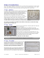
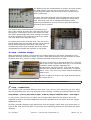
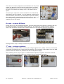
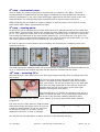
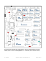
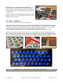
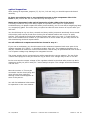
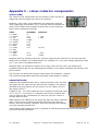
ZXmore
notes for the construction kit
V1.1 07/2015
ZXmore – notes for the construction kit
Seite 1 von 14
Contents
ZXmore.........................................................................................................................1
notes for the construction kit...................................................................................1
Short description:..........................................................................................................3
Before starting:..............................................................................................................3
check components :................................................................................................3
tools/equipment:....................................................................................................3
Order of construction:.....................................................................................................4
1st step - resistors:................................................................................................4
2nd step – diodes:..................................................................................................4
3rd step – IC sockets:.............................................................................................4
4th step – resistor arrays:.......................................................................................5
5th step – capacitors:.............................................................................................5
6th step – crystals & filters:.....................................................................................6
7th step – voltage regulator:...................................................................................6
8th step – mechanical parts:...................................................................................7
9th step – missing parts:.........................................................................................7
10th step – mounting IC's:......................................................................................7
11th step - keyboard:.............................................................................................9
Putting into operation....................................................................................................10
Purpose of connectors and jumpers:.......................................................................10
optical inspection:................................................................................................11
Appendix 1 – parts list of ZXmore:.................................................................................12
resistors:.............................................................................................................12
capacitors:...........................................................................................................12
integrated circuits (ICs):.......................................................................................12
diodes:................................................................................................................13
connectors and jumpers:.......................................................................................13
miscellanous:.......................................................................................................13
optional accessories:.............................................................................................13
Appendix 2 – colour codes for components:.....................................................................14
colour code:.........................................................................................................14
numerical code:....................................................................................................14
V1.1 07/2015
ZXmore – notes for the construction kit
Seite 2 von 14
Short description:
The ZXmore is an 8 bit computer which is compatible to many systems based on the Z80
processor, especially to Sinclair's systems ZX80, ZX81 and ZX Spectrum as well as CP/M
developed by Digital Research (*). ZXmore has an integrated keyboard, a video connector for
a monitor or TV with composite video and a USB interface for loading and storing programs.
A separate serial terminal may be connected via an USB/RS232 adapter but CP/M may be used
with the integrated keyboard and connected video monitor / TV as well (restricted to 40 chars
per line). USB may be used with a flash medium for mass storage. You will need a separate
power supply with 9V/500mA DC while the actual power consumption is about 150mA only.
ZXmore offers 512k flash ROM and 512k RAM, divided into 8 separate instances while the first
instance is used for control the other instances and handling with additional peripheral
hardware (USB for example). The other 7 instances may be configured individually and may
contain different operating systems (or system rom's) either parallel and switched with the
keyboard or concurrently on request (multi tasking system).
You may find more about this and other features in the ZXmore user manual.
(*) The current available release 0.9 of ZXmore does support only system rom's for ZX81 and ZX80 and loading of
programs via the USB flash medium. Future release will support save of program and data on USB flash as well as
using ZX Spectrum rom with monochrome display and support of CP/M. The used roms in the instances running are
covered by the GNU General Public License v2 and may be used free of charge. You will find more notes in the ZXmore
user manual.
Before starting:
check components :
You will need all in the appendix listed parts and components to construct the ZXmore. The
construction kit may be equipped without keyboard or with some special „hard to get“ parts
only. So please check the completeness before starting.
tools/equipment:
You will need the following tools and equipment:
•
•
•
•
•
temperature controlled soldering station with small copper bit
side cutter
tweezer
thin soldering tin
optional – but helpful – is a magnifying lamp or at least a magnifying glass
Soldering is required in 1/10 inch pitch only which isn't too hard even for beginners. But this
shouldn't be your very first soldering project as this is a kind of computer with about 800
soldering joints which requires quite precise work. You may consider some assistance from a
more experienced friend if needed.
The time you need for completion of this construction kit is about 3 hours depending on your
skills.
V1.1 07/2015
ZXmore – notes for the construction kit
Seite 3 von 14
Order of construction:
The easiest way to complete a construction kit is to start with the components in order of their
heigt – the smaller parts first. This way it is easy to lay the board straight on the table.
It would be more easy to start with all equal value components first, step by step.
1st step - resistors:
It is easy to find out all item positions using the imprint of all
component names. Resistors use a rectangle symbol with two
lines as wires, indicating the holes to use. This is quite a
game similar to finding the doors on an advent calendar but
this way you get more familiar with the board also.
All positions for all components are printed on the board.
After every turn the soldering points should be controlled for
maybe forgotten solder joints. This could be done while
holding it against the light to see those candidates or you may
count the solder points during soldering (15 resistors require
30 solder points). This way you are sure not to forget some solder point.
The resistor arrays R1-R7 and SMD resistor R36 are fitted later and should be kept
separate. R9 isn't used at all.
2nd step – diodes:
Diodes may be recognized as a triangle symbol with a bar like
shown in the picture.
Important: All diodes have to be soldered in the right
direction to work. Every diode has a bar printed on the case
and this has to correspond with the bar on the board resp. the
triangle has to point to that bar mark.
Diodes are often too small to print the value/type on it. You
may orient also on the quantity when taking it out of a bag or
the value/type printed on the bag. When finished all solder
joints should be checked as well carefully.
The 3-colour RGB led should be soldered at the end (step 9).
Good time for a short break to keep your concentration !
3rd step – IC sockets:
IC sockets are processed the same way and should be
sorted by size and soldered from the biggest to the
smallest size. This way you can avoid soldering a 14
pin socket in a 16 pin place on the board accidently.
Sockets are aligned by soldering two diagonal edges
first and be sure to put them flat on the board.
Take attention about your fingers when pressing them
on the board while soldering. After fixing one size of
sockets in the edges you should solder row after row
and pin after pin to avoid forgotten solder joints here.
V1.1 07/2015
ZXmore – notes for the construction kit
Seite 4 von 14
The ZXmore has two modifications in revision one and contain
one SMD resistor inserted into one track and a small wire
connecting two tracks. One end of this wire is quite near to
IC14 (74HCT245).
The pins should be soldered from the opposite side to avoid
releasing the wire accidently when holding the copper bit to
near. Also keep note not to damage the isolation when
soldering the capacitor in front of the IC later and hold the
wire back with a tweezer.
The square PLCC socket sould be mounted prior to
the 14 pin sockets as there are some narrows due to
the big size. It should be fixed in the same way with
two solder points diagonally while moving the socket
as far as possible to the connector side of the board.
The drills allow some backlash here.
It is quite narrow with C16 and IC12. The pin of C16
should match into the drill hole and the 14 pin socket
below should match as well. Note: The parts list
contains two extra 14 pin sockets which are used to
compensate the height and narrows on the board.
4th step – resistor arrays:
After mounting all sockets you can place the resistor arrays on the board. Important is the
direction while the arrays are coded. The two 2.2k arrays R6 and R7 can be mounted in either
direction while they contain 5 single resistors with both ends wired (10 pins).
The other arrays have to be placed with pin 1 marked
with a star on the component while pin 1 on the board
is marked with a optically separated pin.
On the picture you can see the 4.7k array R1 which
shouldn't be confused with R11 while pin 1 is marked
with a 1 too, very near to R1 which may be accidently
read as R11.
Be sure to place all arrays in the right direction which
isn't same for all !
Good time for a short break to keep your concentration !
5th step – capacitors:
The capacitors are used with different pitch with 1/10, 2/10 or 3/10 inches. If you don't have
the corresponding pitch you may bend the wires carefully to match the required pitch as well.
C34 (150pF, 1/20 in) and C33 (470pF, 1/20 in) may be soldered later – see step 9.
C1,C2,C6,C31 (100uF) and C5 (22uF) are processed later because the polarity has to be
regarded as well as all 100nF capacitors should be spreaded over the board as power supply
stabilization only.
All other (named) capacitors are placed first, then the bigger 100nF with 3/10 inches pitch in
front of IC3, IC4, IC15 und IC20. If you don't have matching pitches you may bend the wires
carefully.
V1.1 07/2015
ZXmore – notes for the construction kit
Seite 5 von 14
The other 13 ceramic capacitors for stabilization of the power
supply are placed in front of the IC's marked with a symbol
with two parallel lines and 2 wire indicating the drill holes to
be used. The names are missing here on the board due to
space.
All electrolytic capacitors and the tantalum are soldered last
and always with the marked + on the capacitor matching the
drill hole with a plus mark. The electrolytic caps have mostly
the negative wire marked with a big bar or minus – this way
the corresponding pin should NOT be matched with the
marked plus on the board.
6th step – crystals & filters:
Finally it's turn for the crystals and filters. The3 pin filter with 6.5 MHz has no polarity and can
be simply mounted on it's space marked with X1. The other two crystals have no polarity
either and should be mounted with a small distance to the board as shown in the pictures.
Putting the RTC chip in the 8pin socket will protect the small crystal against mechanical stress.
7th step – voltage regulator:
The following 3 pictures show mounting the voltage regulator IC1 (7805). First the red marked
via should be isolated from contact with the heatsink. The regulator is decoupled from the GND
potential with two diodes for possible use with a USB power supply.
After isolating with a drop of glue or a small stripe of tape the regulator should be mounted
with a screw first and then solder the contacts to avoid mechanical strength.
V1.1 07/2015
ZXmore – notes for the construction kit
Seite 6 von 14
8th step – mechanical parts:
Time to solder the missing connectors, switches and pin headers in it's place. The small
contacts should be soldered first and the bigger connecting the case at last with increased
soldering temperature. The outer cases and bigger copper areas will take much of the heat
from the solder iron and this may take several seconds to let the solder melt nicely.
When soldering the pin headers it might be helpful to place a jumper first to hold it on that
point safely with a finger (protected from heat).
9th step – missing parts:
So there are now 4 components not used which have to be placed manually at the solder side
of the board. The left picture shows C34 (150pF) at IC24 (74HCT373) connected to pin 10 and
pin 11. The middle pic shows C33 at IC8 (74AHCT08) connected to pin 7 and pin 10 while the
next shows the placement of the smd resistor between pin 1 of J10 and pin 14 of IC12. The
last picture shows a wanted short between IC23 pin 9 and 10 made with plain solder. You may
use a wire instead as well if it is too difficult for you (a bit tricky).
Be sure to take the correct position and remember the mirrored pin numbering when seen
from the back side.
The RGB LED can be soldered finally, too. It should have a distance to the board of about 2/10
up to ½ inches and the longest leg goes into the drill hole marked with the point.
10th step – mounting IC's:
New ICs have pin rows which have to be first right-angled manually prior to putting them into
the sockets.
You have to bend all pins right-angle like shown in the
picture. You take the body between right and left hand
with your fingers, let one line of pins lay on the table and
then turn the body a little bit to bend all pins slowly all
together with not too much power in the right angle
direction (90 degrees from body).
This must be done in a careful and sensitive way and it is
better to repeat this step 1 or 2 times than to bend them
too much in the first step. Bending should be done
alternately from both sides. This is just a matter of excercise and will be easier with the
smaller ICs.
The best way is to start with the small ICs and
after proceed with the bigger ones. So you get
a little bit routined and it is not too annoying
to damage a cheap TTL IC which can be
replaced inexpensive in case of damage.
You will find an overview where to place which IC in the following drawing:
V1.1 07/2015
ZXmore – notes for the construction kit
Seite 7 von 14
In the picture the red marks show jumpers to be set and which position while the cyan/blue
marked jumper is optional for setting up ZXmore for NTSC video (default PAL when not set).
V1.1 07/2015
ZXmore – notes for the construction kit
Seite 8 von 14
The two with *** marked sockets needed with
additional height because they are two narrowed to
their neighbour. You simply put a second IC socket in
the soldered IC socket (recommended with precision
sockets only).
The picture shows the double stacked sockets in their
position. That's why the component list has two more
sockets than 14 pin IC's.
11th step - keyboard:
There are two variants of mounting a keyboard.
The original keyboard membrane from Sinclair is self-adhesive and has metallized holes under
each key to connect the wire tracks under it when pressing keys. The small holes in the edges
may help to put the keyboard membrane right in place. Especially the bottom holes should
match exactly to the board holes if you want mount the board into a case.
A new keyboard membrane may have to be used quite long time to get easier to work.
The second variant uses smd tactile switches for a comfortable use of the keyboard with less
force. The keys are soldered first in their place and then the small doublesided adhesive tape
will be put around the keys as shown. Be sure to match the outer lines of the membrane which
is put on top of the tape after. The tape matches the additional height of the switches.
Good time for a short break to keep your concentration !
V1.1 07/2015
ZXmore – notes for the construction kit
Seite 9 von 14
Putting into operation
First you should get familiar with all connectors of the system and jumpers to be set.
Purpose of connectors and jumpers:
J1
slot edge connector for additional hardware mounted to the ZXmore
like printers, mass storage devices like ZXpand and interfaces available for ZX81
J2
power connector 3.5mm audio jack for power supply of 9V to 12V DC
polarity: tip for plus and ring for minus
J3
EAR, 3.5mm audio jack for LOAD (load programs)
J4
MIC, 3.5mm audio jack for SAVE (save programs)
J5
Video, chinch jack, composite video output (monochrome)
J6
USB, 2x USB host port for mass storage & peripherals
J7
power jumper, may be used for a power switch, must be set on operation
J8
RAM size, jumper has to be set to board connectors direction
J9
reset, may be used for an additional reset switch when mounting into a case
J10
boot, must be set to keyboard direction (see user manual)
J11
used for programming the USB controller – for development purposes only
J12
I/O address used for latches, default set to A7 (see user manual)
J13
video mode – PAL for not set, NTSC for set
J14/J15 connectors for external keyboard (see user manual)
J16
video polarity, set to connectors direction for normal picture,
vice-versa for inverted picture (white chars on black background)
J17
rom switch, for mechanical switching of instances, should be kept to „0“
(for details see user manual)
J18
onboard reset switch for soft reset (see user manual)
J19
battery holder for CR1220 battery, used for the RTC chip (clock)
V1.1 07/2015
ZXmore – notes for the construction kit
Seite 10 von 14
optical inspection:
After setting all important jumpers (J7, J8, J10, J12 und J16) you should inspect the board
carefully.
Is there any missing part or any marked free area on the component side of the
board ? (R9, J9 and J11 are not used and may be kept free.)
Much more important is the optical inspection of the solder side of the board.
A missing connection may have deep impact on operation and require a sophisticated
troubleshooting. So please inspect all solder joints carefully, row to row with a magnifying lamp
or a magnifying glass. The more time you spend on this the more chance of a quick start you
will have.
You should keep an eye on clean, smooth and shiny solder joints and accidently shorts made.
Cold solder joints can be found when looking for tarnished surface and uneven or spiky
surface. They should be fixed while soldering again with some very rare (!) fresh solder tin.
Here is the contained flux needed. If you have much to much solder tin you may remove all
with desoldering wick and repeat solder.
Are all additional components added as shown in step 9 ?
If you own a multimeter you should measure the resistance between both outer pins of the
voltage regulator IC1 (7805) – it should be greater than 10k. The resistance between pin 2
and pin 3 should be minimum a few hundred ohms. Shorts may be problematical here as 9V or
12V of power voltage may damage the integrated circuits.
The power supply can be connected now while regarding the correct polarity. The tip of the
3.5mm audio plug has to be plus and the ring is minus. The voltage may be 9V or 12V DC.
In the next step the output voltage of the regulator should be checked after power-up while
measuring at any 14 pin IC with pin 7 minus and pin14 plus. The voltage should be between
4.8 and 5.1V.
Now the monitor or TV may be
connected via the chinch plug and
when all was done right the
starting screen should appear as
seen in the picture.
You will find additional information
for operation in the user manual.
V1.1 07/2015
ZXmore – notes for the construction kit
Seite 11 von 14
Appendix 1 – parts list of ZXmore:
resistors:
4x
1x
2x
5x
10 x
1x
2x
2x
2x
1x
4x
1x
33R
R12,R13,R14,R15
220R
R30
330R
R21,R31
680R
R20,R22,R27,R28,R33
1k
R8,R10,R17,R19,R24,R25,R29,R32,R34,R35
3k3
R26
10k
R11,R23
100k
R16,R18
Array, 2k2, 5x parallel (10 pin), R6,R7
Array, 4k7, 8x star (9 pin), R1
Array, 10k, 8x star (9 pin), R2,R3,R4,R5
10k SMD 1206, R36
capacitors:
3 x 18pF, RM 2.5 C7, C14, C15 (alternative 15pF)
1 x 47pF, RM 2.5 C16
1 x 68pF, RM 2.5 C12
1 x 150pF, RM 5
C34
1 x 330pF, RM 2.5 C13
1 x 470pF, RM 2.5 C4,
1 x 470pF, RM 5
C33
1x
1nF, RM 5
C8
2 x 47nF, RM 5
C9,C11
13 x 100nF, RM 5
C3,C10,C17,C18,C19,C20,C21,C23,C24,C25,C26,C29,C30,C32
4 x 100nF, RM 7.5 C20, C22, C27, C28
1 x 22uF/16V, RM 2.5, tantal C5
4 x 100uF/16V, 6.3mm, C1,C2,C6,C31
integrated circuits (ICs):
1
1
1
1
1
1
2
1
1
2
1
1
1
1
1
2
3
1
1
1
1
1
x
x
x
x
x
x
x
x
x
x
x
x
x
x
x
x
x
x
x
x
x
x
7805
IC1 (voltage regulator TO220, alt. LMS78_05-1.0, RECOM R-785.0-1.0)
Z84C0008 IC2 (Zilog Z80 CPU, 8 Mhz, DIP40)
AS6C4008 IC3 (SRAM 512 kByte, DIP32)
SST39SF040 IC4 (Flash ROM, 512k Byte, DIP32)
74AC86
IC21 (DIP14, only advanced CMOS, no ACT, no HCT, no HC)
74HC590
IC11 (DIP16)
74HCT00
IC10,IC20 (DIP14)
74HCT04
IC6 (DIP14)
74AHCT08 IC8 (DIP14)
74HCT32
IC7,IC23 (DIP14)
74AHCT74 IC19 (DIP14)
74HCT85
IC17 (DIP16)
74HCT125 IC12 (DIP14)
74AHCT126 IC9 (DIP14)
74HCT165 IC15 (DIP16)
74HCT245 IC5,IC16 (DIP20)
74HCT373 IC14,IC22,IC24 (DIP20)
74HCT393 IC18 (DIP14)
74HCT40103 IC13 (DIP16)
VNC2-32L1B IC25 (LQFP32)
EPM3032ALC44-10N, IC26 (PLCC44)
DS1302
IC27 (DIP8)
V1.1 07/2015
ZXmore – notes for the construction kit
Seite 12 von 14
diodes:
17 x BAT46
2 x 1N4148
1 x 1N5817
1 x LED RGB
D1,D4,D5,D6,D7,D10,D11,D12,D13,D14,D15,D16,D17,D18,D19,D20,D21
D8,D9
D2
D3, common anode
connectors and jumpers:
3
1
1
1
1
1
x CL1384
J2,J3,J4 (3.5mm audio jack mono, manufacturer CLIFF)
x S8411-45R J19 (CR1220 battery holder, SMD, manufacturer Harwin)
x Chinch
J5 (female, right-angled, pcb version, RM 11mm)
x USB plug
J6 (USB plug female, 2-port, right-angled, pcb version)
x KDR16H
J17 (ROM switch, hex coded switch, right-angled, manufacturer OTAX)
x MJTP1105 J18 (Reset switch, right-angled, pcb version, manufacturer APEM)
6 x Jumper
for 2-pin male pinheads
3 x pinhead male 1x2, J7,J9,J13
3 x pinhead male 1x3, J8,J10,J16
1 x pinhead male 2x5, J12
optional:
1 x pin head female 1x5 right-angled, J14 (for external keyboard ZX8-KDLX)
1 x pin head female 1x8 right-angled, J15 (for external keyboard ZX8-KDLX)
J1 is the slot edge connector directly on the pcb and is not to be mounted. :-)
miscellanous:
1 x DIP8
IC socket, precision socket with gold plated contacts
13 x DIP14
IC socket, precision socket with gold plated contacts
4 x DIP16
IC socket, precision socket with gold plated contacts
5 x DIP20
IC socket, precision socket with gold plated contacts
2 x DIP32
IC socket, precision socket with gold plated contacts
1 x DIP40
IC socket, precision socket with gold plated contacts
1 x PLCC44
IC socket PLCC
1 x 12 MHz
X2, crystal, HC49U, 12.000 MHz
1 x 32.768kHz X3, crystel, 2.1 x 6 mm, 6pF, clock crystal
1 x 6.5 MHz
X1, SFE 6.5, ZF filter 6.5 MHz, (Murata)
1 x 1uH
L1, inductance, RM 12.5, alt. other values between 1 und 5 uH
1 x CR1220
battery 3V
1 x heatsink for TO220, max. 23 x 17 mm (length/width) with screw
1 x pcb board Zxmore, 204 x 156 mm, 2 layers
1 x keyboard ZX80 keyboard membrane
optional:
40 x ALPS
SMD tactile switches Alps, SKQGAFE010, 1 newton force
(can be combined with ZX80 keyboard membrane for better typeing)
optional accessories:
1
1
1
1
1
x
x
x
x
x
power supply, 9V DC, 500mA, with jack 3.5mm
cable, 3-5 meters with 3.5mm audio jack mono
cable, 1-3 meters chinch shielded for monitor/TV connection
USB flash stick as mass storage
USB adapter RS232, CHIPI-X from FTDI, for serial terminal connection with CP/M
V1.1 07/2015
ZXmore – notes for the construction kit
Seite 13 von 14
Appendix 2 – colour codes for components:
colour code:
The value of most components are not printed in clear text due to
shape and size but coded with colours or numbers.
Resistors, coils, rarely some capacitors are coded with coloured
rings. Depending on precision 2 or 3 rings are used to indicate the
value, the forelast is the multiplier and the last one the tolerance.
Every colour represents one digit.
value
0 = black
1 = brown
2 = red
3 = orange
4 = yellow
5 = green
6 = blue
7 = violet
8 = grey
9 = white
* = gold
* = silver
multiplier
x1
x10
x100
x1000
x104
x105
x106
x107
tolerance
x0.1
x0.01
( 5%)
(10%)
( 1%)
( 2%)
(0,1%)
Resistors with 5% tolerance have four coloured rings with the first two for the value and the
third for the multiplier. For example black is a multiplier of 1 (100) and orange represents 1000
(103). The value is multiplied with this.
Resistors with 1% tolerance or better own 5 rings, three for the value, the following as
mutliplier and the last one for indicating the tolerance. Two resistor examples are shown in the
picture above.
The first has 330 ohms with orange-orange-black and multiplier 1 (black).
The second has 680 ohms with blue-grey-black and multiplier 1 (black).
numerical code:
Capacitors are specified often with a 3 digit numerical code. The first
two digits give the value and the last one the multiplier. The value is
specified in pF (pico Farad). On the picture you see 150pF (15*101)
and 470pF (47*101).
1000pF is 1nF – so a 10nF capacitor has an imprint of numerical code
103 = 10*103 = 10.000 pF or a capacitor with 10uF is marked with
106 (10.000.000 pF). Sometimes you may see just 10u if there is
enough space to print.
SMD resistors are classified in the same way with the same numerical
code. In the picture 2 resistors with 220 ohms and 330 ohms are
shown. There are existing „resistors“ with zero ohms as well marked
only with a simple printed zero.
Unfortunately SMD capacitors have no imprints at all and should be taken from their packing
only when directly processed.
V1.1 07/2015
ZXmore – notes for the construction kit
Seite 14 von 14