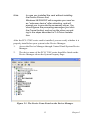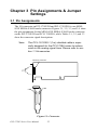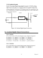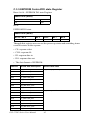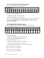
1
PCI-1758U Series
128-Channel Isolated Digital
Input/Output Card
User Manual
Copyright
The documentation and the software included with this product are copyrighted 2005 by Advantech Co., Ltd. All rights are reserved. Advantech
Co., Ltd. reserves the right to make improvements in the products
described in this manual at any time without notice. No part of this manual may be reproduced, copied, translated or transmitted in any form or
by any means without the prior written permission of Advantech Co., Ltd.
Information provided in this manual is intended to be accurate and reliable. However, Advantech Co., Ltd. assumes no responsibility for its use,
nor for any infringements of the rights of third parties, which may result
from its use.
Acknowledgements
PC-LabCard is a trademark of Advantech Co., Ltd. IBM and PC are
trademarks of International Business Machines Corporation. MS-DOS,
Windows®, Microsoft® Visual C++ and Visual BASIC are trademarks of
Microsoft® Corporation. Intel® and Pentium® are trademarks of Intel
Corporation. Delphi and C++ Builder are trademarks of Inprise Corporation.
Part No. 2003175801
2nd Edition
Printed in Taiwan
May 2005
PCI-1758U Series User Manual
ii
Product Warranty (2 years)
Advantech warrants to you, the original purchaser, that each of its products will be free from defects in materials and workmanship for two years
from the date of purchase.
This warranty does not apply to any products which have been repaired or
altered by persons other than repair personnel authorized by Advantech,
or which have been subject to misuse, abuse, accident or improper installation. Advantech assumes no liability under the terms of this warranty as
a consequence of such events.
Because of Advantech’s high quality-control standards and rigorous testing, most of our customers never need to use our repair service. If an
Advantech product is defective, it will be repaired or replaced at no
charge during the warranty period. For out-of-warranty repairs, you will
be billed according to the cost of replacement materials, service time and
freight. Please consult your dealer for more details.
If you think you have a defective product, follow these steps:
1.
Collect all the information about the problem encountered. (For
example, CPU speed, Advantech products used, other hardware
and software used, etc.) Note anything abnormal and list any
onscreen messages you get when the problem occurs.
2.
Call your dealer and describe the problem. Please have your manual, product, and any helpful information readily available.
3.
If your product is diagnosed as defective, obtain an RMA (return
merchandize authorization) number from your dealer. This allows
us to process your return more quickly.
4.
Carefully pack the defective product, a fully-completed Repair and
Replacement Order Card and a photocopy proof of purchase date
(such as your sales receipt) in a shippable container. A product
returned without proof of the purchase date is not eligible for warranty service.
5.
Write the RMA number visibly on the outside of the package and
ship it prepaid to your dealer.
iii
CE
All products in the PCI-1758U Series have passed the CE test for environmental specifications when shielded cables are used for external wiring. We recommend the use of shielded cables. This kind of cable is
available from Advantech. Please contact your local supplier for ordering
information.
Technical Support and Assistance
Step 1. Visit the Advantech web site at www.advantech.com/support
where you can find the latest information about the product.
Step 2. Contact your distributor, sales representative, or Advantech's customer service center for technical support if you need additional
assistance. Please have the following information ready before
you call:
- Product name and serial number
- Description of your peripheral attachments
- Description of your software (operating system, version, application software, etc.)
- A complete description of the problem
- The exact wording of any error messages
Packing List
Before setting up the system, check that the items listed below are
included and in good condition. If any item does not accord with the
table, please contact your dealer immediately.
The PCI-1758U include the following items:
1 x PCI-1758UDI, PCI-1758UDO or PCI-1758UDIO card
1 x Companion CD-ROM (DLL driver included)
1 x User Manual (This manual)
PCI-1758U Series User Manual
iv
Contents
Chapter
Chapter
1 General Information ....................................... 2
1.1
Introduction ....................................................................... 2
1.2
Installation Guide .............................................................. 6
1.3
Accessories........................................................................ 8
1.1.1
Figure 1.1:Installation Flow Chart ................................. 7
1.3.1
1.3.2
PCL-101100S-1 Wiring Cable ....................................... 8
ADAM-39100 Wiring Terminal Board ......................... 8
2 Installation ..................................................... 10
2.1
2.2
Unpacking ....................................................................... 10
Driver Installation ........................................................... 11
2.3
Hardware Installation ...................................................... 14
2.4
Device Setup & Configuration........................................ 16
Figure 2.1:The Setup Screen of Advantech Automation
Software ........................................................... 12
Figure 2.2:Different Options for Driver Installation ... 13
Figure 2.3:The Device Name Listed on Device Mng .. 15
2.4.1
2.4.2
Chapter
Features .......................................................................... 2
Table 1.1:PCI-1758U Series Features Comparison ....... 6
Setting Up the Device .................................................. 16
Figure 2.4:The Device Manager Dialog Box ............... 17
Figure 2.5:The “Device(s) Found” Dialog Box ........... 17
Configuring the Device ................................................ 18
Figure 2.6:The Device Setting Dialog Box ................. 18
Figure 2.7:The Device Name Appearing on the List of
Devices Box ..................................................... 19
Figure 2.8:The Test Diagram Box for Digital Input .... 20
Figure 2.9:The Test Diagram Box for Digital Output 20
3 Pin Assignments & Jumper Settings ........... 22
3.1
Pin Assignments.............................................................. 22
3.2
Location of Jumpers and DIP Switch.............................. 29
Figure 3.1:Connector ................................................... 22
Figure 3.2:I/O Conn.Pin Assig. for PCI-1758UDI ...... 23
Figure 3.3:I/O Conn. Pin Assig. for PCI-1758UDO .... 24
Figure 3.4:I/O Conn. Pin Assig. for PCI-1758UDIO .. 25
Table 3.1:PCI-1758UDI I/O Conn. Signal Desc. ........ 26
Table 3.2:PCI-1758UDO I/O Connector Signal Desc. 27
Table 3.3:PCI-1758UDIO I/O Conn. Signal Desc. ..... 28
Figure 3.5:Location of DIP Switch on PCI-1758UDI . 29
Figure 3.6:Location of DIP Switch and Jumper on PCI1758UDO ......................................................... 29
Figure 3.7:Location of DIP Switch and Jumper on PCI1758UDIO ....................................................... 30
v
Table of Contents
3.3
3.4
Isolated Digital Input Connections.................................. 30
3.3.1
3.3.2
Isolated Digital Output Connections ............................... 31
3.4.1
3.4.2
3.5
3.6
Chapter
Interrupt Function of the DI Signals ............................ 30
Isolated Inputs .............................................................. 31
Figure 3.8:Isolated Digital Input Connection .............. 31
Power On Configuration .............................................. 32
Table 3.4:JP1: Power On Config. after Hot Reset ....... 32
Isolated Outputs ........................................................... 32
Figure 3.9:Isolated Digital Output Connection ............ 33
Field Wiring Considerations ........................................... 33
Setting the BoardID Switch (SW1)................................. 34
Table 3.5:Board ID Setting (SW1) .............................. 34
4 Operation ....................................................... 36
4.1
Interrupt Function (PCI-1758UDI/UDIO) ...................... 36
4.2
Digital Filter Function (PCI-1758UDI/UDIO) ............... 37
4.1.1
4.1.2
4.2.1
4.2.2
4.3
4.4
4.5
IRQ Level .................................................................... 36
Interrupt Modes for Digital Input ................................ 36
Figure 4.1:Interrupt Mode for Digital Input ................ 36
Table 4.1:Pulse Width Filtering ................................... 37
Digital Filtering Example ............................................ 38
Figure 4.2:Digital Filter Example ................................ 38
Digital Filter Function Control Register ...................... 38
Watchdog Timer Function (PCI-1758UDO/UDIO) ....... 39
Power-Up States Function (PCI-1758UDO/UDIO)........ 39
BoardID........................................................................... 40
Table 4.2:BoardID Reg. of PCI-1758UDI/1758UDO . 40
Table 4.3:BoardID Setting (SW1) ............................... 40
Appendix A Specifications ................................................. 42
A.1
A.2
A.3
A.4
PCI-1758UDI .................................................................. 42
PCI-1758UDO................................................................. 42
PCI-1758UDIO ............................................................... 43
General ............................................................................ 44
Appendix B Block Diagram ............................................... 46
B.1
B.2
B.3
PCI-1758UDI Block Diagram......................................... 46
PCI-1758UDO Block Diagram ....................................... 47
PCI-1758UDIO Block Diagram...................................... 47
Appendix C Register Structure & Format ....................... 50
C.1
C.2
Register Structure............................................................ 50
PCI-1758UDI Register Format ...................................... 50
C.2.1
C.2.2
C.2.3
C.2.4
C.2.5
C.2.6
C.2.7
Register Format ............................................................ 50
Digital Input Register ................................................... 52
Digital Input Rising Edge Interrupt Register ............... 53
Digital Input Falling Edge Interrupt Register .............. 54
Interrupt State Register ................................................ 55
Interrupt of Port Identify Register ............................... 56
Digital Filter Function Control Register ..................... 56
PCI-1758U Series User Manual
vi
C.2.8
C.3
C.4
C.5
Filter Interval Time Preset Register ............................. 57
PCI-1758 UDO Register Format..................................... 58
C.3.1
C.3.2
C.3.3
C.3.4
C.3.5
Digital Output Register ............................................... 59
Watchdog Counter Value Register ............................. 60
Watchdog State/Control Register ................................ 60
Watchdog Timer Clear Register .................................. 61
EEPROM Control/DO state Register .......................... 62
PCI-1758UDIO Register Format .................................... 63
C.4.1
C.4.2
C.4.3
C.4.4
C.4.5
C.4.6
C.4.7
C.4.8
C.4.9
C.4.10
C.4.11
C.4.12
C.4.13
Register Format ............................................................ 63
Digital input Register .................................................. 64
Digital Output Register ............................................... 65
Digital input Ring Edge Interrupt Register ................. 66
Digital input Falling Edge Interrupt Register ............. 66
Interrupt State Register ................................................ 67
Interrupt Of Port Identify Register .............................. 68
Digital Filter Enable Register ..................................... 68
Filter Interview Time Preset Register .......................... 69
Watchdog Counter Value Register .............................. 70
Watchdog State/Control Register ............................... 70
Watchdog Time Clear Register ................................... 71
EEPROM Control/DO state Register .......................... 72
BoardID Register............................................................. 73
vii
Table of Contents
PCI-1758U Series User Manual
viii
CHAPTER
1
2
General Information
This chapter gives background information on the cards in the PCI-1758U
Series. It then shows how to configure
the cards to match your application and
prepare them for installation on your
system.
Sections include:
• Introduction
• Installation Guide
• Accessories
Chapter 1 General Information
1.1 Introduction
Thank you for buying a PCI-1758U Series digital input/output card. The
PCI-1758U cards enable powerful data acquisition (DAS) for the PCI
bus. It features a unique circuit design, and complete functions for data
acquisition and control.
The PCI-1758U cards provides specific functions for different user
requirements:
PCI-1758UDO
128-channel Isolated Digital Output card
PCI-1758UDI
128-channel Isolated Digital Input Card
PCI-1758UDIO
64-channel Isolated Digital Input and
64-channel Isolated Output Card
The following sections of this chapter will provide further information
about features of the DAS cards.
1.1.1 Features
PCI-1758U cards provide the most requested I/O and control functions as
seen below:
PCI-1758UDO
• 128 isolated digital output channels
• High-voltage isolation on output channels (2,500 V DC )
• Wide output range (5 ~ 40 V DC )
• High-sink current for isolated output channels (90 mA max./Channel)
• Current protection for each port
• BoardID Switch
• Output status read-back
• Digital output value retained after hot system reset
• Programmable Power-Up States
• Watchdog Timer
PCI-1758U Series User Manual
2
PCI-1758UDI
• 128 isolated digital input channels
• High-voltage isolation for input channels (2,500 VDC )
• Wide input range (5 ~ 25 VDC )
• High ESD Protection (2,000 VDC)
• Digital Filter function
• BoardID Switch
• Interrupt handling capability
PCI-1758UDIO
Digital Output
• 64 isolated digital output channels
• High-voltage isolation on output channels (2,500 VDC )
• Wide output range (5 ~ 40 VDC )
• High-sink current for isolated output channels (90 mA max./Channel)
• Current protection for each port
• Output status read-back
• Digital output value retained after hot system reset
• Programmable Power-Up States
• Watchdog Timer
Digital Input
• 64 isolated digital input channels
• High-voltage isolation for input channels (2,500 VDC )
• Wide input range (5 ~ 25 VDC )
• High ESD protection (2,000 VDC )
• Digital Filter function
• Interrupt handling capability
• Robust isolation
• BoardID switch
3
Chapter 1
Robust Isolation
PCI-1758U cards feature a robust isolation protection for applications in
industrial, lab and machinery automation. The PCI-1758U cards can
durably withstand a voltage up to 2,500 VDC, preventing your host system from any incidental harms.
Wide Input/Output Range
PCI-1758U cards have a wide range of input voltage and it is suitable for
most industrial applications with 12 VDC and 24 VDC input voltage. The
PCI-1758U cards also feature a wide output voltage range, suitable for
most industrial applications with 12 VDC / 24 VDC output voltage. In the
mean time, we are also ready to serve your special needs for specific
input/output voltage range.
PCI-1758UDI
• Input range: 5~25 VDC
PCI-1758UDO
• Output range: 5~40 VDC
PCI-1758UDIO
• Input range: 5~25 VDC
• Output range: 5~40 VDC
BoardID Switch
PCI-1758U cards have a built-in DIP switch that helps define each card’s
ID when multiple cards have been installed on the same PC chassis. The
BoardID switch is very useful when you are building a system with multiple PCI-1758U cards. With correct BoardID settings, you can easily identify and access each card during hardware configuration and software
programming.
PCI-1758U Series User Manual
4
Programmable Power-Up States Function (PCI-1758UDO/UDIO)
When powering up, the output drives on PCI-1758UDO/UDIO are disabled. All output lines are user-configurable for logic high output and
logic low output. User-configurable power-up states are useful for ensuring that the PCI-1758UDO/UDIO powers up in a known state. Power-up
states are programmed in the EEPROM through the driver. The default
settings are all set to 0. For more details, please refer to Appendix C.
Watchdog Timer Function
The watchdog timer is a software-configurable feature used to set critical
outputs to safe states in the event of a software failure. It will activate if
there is a loss of communication between the application and the PCI1758U card. If the PCI-1758U card does not receive a watchdog clear
software command within the interval time specified for the watchdog
timer, the outputs go to a user-defined safe state and remain in that state
until the watchdog timer is disabled and new values are written by the
software.
After the watchdog timer expires, the PCI-1758U card ignores any writes
until the watchdog timer is disabled. Users can set the watchdog timer
timeout period through WDT register to specify the amount of time that
must elapse before the watchdog timer expires. The counter on the watchdog timer is configurable up to (232-1) x 100 ns (approximately seven
minutes) before it expires.
Reset Protection
If the system has undergone a hot reset (i.e. without turning off the system power), the PCI-1758UDO/UDIO can either retain outputs values of
each channel, or return to its default configuration with power up status,
depending on its onboard jumper setting. This function protects the system from causing wrong operations during unexpected system resets.
5
Chapter 1
Table 1.1: PCI-1758U Series Features Comparison
PCI BUS Isolated Digital
I/O card
PCI-1758UDIO
PCI-1758UDO
PCI-1758UDI
Isolated Digital Input
Y (64-ch)
Y (128-ch)
-
Isolated Digital Output
Y (64-ch)
-
Y (128-ch)
BoardID
Y
Y
Y
2500 VDC Isolation
Y
Y
Y
Wide Input Range
Y
(5~25 VDC)
-
Y
(5~25 VDC)
Wide Output Range
Y
(5~40 VDC)
Y
(5~40 VDC)
-
Keep last status after hot
reset
Y
Y
-
High Sink current on IDO
channels
Y
(90 mA/ch)
Y
(90mA/ch)
-
Output status read back
Y
Y
-
Interrupt handling
Y
-
Y
ESD protection
Y (2000VDC)
-
Y (2000VDC)
1.2 Installation Guide
Before you install your PCI-1758U card, please make sure you have the
following necessary components:
• PCI-1758UDI, PCI-1758UDO or PCI-1758UDIO isolated digital I/O
card
• PCI-1758U Series User Manual
• Driver software: Advantech DLL drivers(included in the companion
CD-ROM)
• Wiring cable: 100-pin MINI-SCSI HDRA-E100 cable
• Wiring board: ADAM-39100
• Computer: Personal computer or workstation with a PCI-bus slot (running Windows 98/2000/XP)
PCI-1758U Series User Manual
6
After you get the necessary components and maybe some accessories for
enhanced operation for your DAS card, you can then begin the installation procedure. Figure 1-1 provides a concise flow chart to give users a
broad picture of the software and hardware installation procedure.
Install Driver from CDROM, then turn off power
Install hardware and turn on the PC
Use driver utility to configure hardware
Use test utility to test hardware
Read examples and driver manual
Start to write your own application
Figure 1.1: Installation Flow Chart
7
Chapter 1
1.3 Accessories
Advantech offers a complete set of accessory products to support the
PCI-1758UDI / 1758UDO cards. These accessories include:
1.3.1 PCL-101100S-1 Wiring Cable
The PCL-101100S-1 (1m) shielded cable is specially designed for the
PCI-1758UDI/UDO card to provide high resistance to noise.
1.3.2 ADAM-39100 Wiring Terminal Board
ADAM-39100 is a 100-pin SCSI wiring terminal module for DIN-rail
mounting. This terminal module can be readily connected to Advantech
PC-LabCard products and allow easy and reliable access to individual pin
connections for the PCI-1758UDI/UDO card.
PCI-1758U Series User Manual
8
CHAPTER
2
2
Installation
This chapter gives users a package item
checklist, proper instructions about
unpacking and step-by-step procedures
for both driver and card installation.
Sections include:
• Unpacking
• Driver Installation
• Hardware Installation
• Device Setup and Configuration
Chapter 2 Installation
2.1 Unpacking
After receiving your PCI-1758U product package, please inspect its contents first. The package should contain the following items:
• PCI-1758UDI, PCI-1758UDO or PCI-1758UDIO card
• Companion CD-ROM (Device Drivers included)
• User Manual
The PCI-1758U cards harbor certain electronic components vulnerable to
electrostatic discharge (ESD). ESD could easily damage the integrated
circuits and certain components if preventive measures are not carefully
paid attention to.
Before removing the card from the antistatic plastic bag, you should take
following precautions to ward off possible ESD damage:
• Touch the metal part of your computer chassis with your hand to discharge static electricity accumulated on your body. Or one can also use
a grounding strap.
• Touch the anti-static bag to a metal part of your computer chassis
before opening the bag.
• Take hold of the card only by the metal bracket when removing it out of
the bag.
After taking out the card, you should first:
• Inspect the card for any possible signs of external damage (loose or
damaged components, etc.). If the card is visibly damaged, please
notify our service department or our local sales representative immediately. Avoid installing a damaged card into your system.
Also pay extra caution to the following aspects to ensure proper
installation:
• Avoid physical contact with materials that could hold static electricity
such as plastic, vinyl and Styrofoam.
• Whenever you handle the card, grasp it only by its edges. DO NOT
TOUCH the exposed metal pins of the connector or the electronic components.
PCI-1758U Series User Manual
10
Note
Keep the anti-static bag for future use. You might
need the original bag to store the card if you
have to remove the card from PC or transport it
elsewhere.
2.2 Driver Installation
We recommend you to install the driver before you install the PCI1758U series card into your system, since this will guarantee a
smooth installation process.
The Advantech Device Driver Setup program for the PCI-1758U series
card is included on the companion CD-ROM that is shipped with your
DA&C card package. Please follow the steps below to install the driver
software:
1.
Insert the companion CD-ROM into your CD-ROM drive.
2.
The Setup program will be launched automatically if you have the
autoplay function enabled on your system. When the Setup Program is launched, you’ll see the following Setup Screen.
Note
If the autoplay function is not enabled on your
computer, use Windows Explorer or Windows
Run command to execute Autorun.exe on the
companion CD-ROM.
11
Chapter 2
Figure 2.1: The Setup Screen of Advantech Automation Software
3.
Select the Individual Drivers option.
4.
Select the specific device then just follow the installation instructions step by step to complete your device driver installation and
setup.
PCI-1758U Series User Manual
12
Figure 2.2: Different Options for Driver Installation
For further information on driver-related issues, an online version of the
Device Drivers Manual is available by accessing the following path:
Start\Programs\Advantech Automation\Device Manager\Device
Driver’s Manual
13
Chapter 2
2.3 Hardware Installation
Note
Make sure you have installed the driver before
you install the card.
(please refer to 2.2 Driver Installation)
After the device driver installation is completed, you can now go on to
install the PCI-1758U series card in any PCI slot on your computer. But it
is suggested that you refer to the computer user manual or related documentation if you have any doubt. Please follow the steps below to install
the card on your system.
1.
Turn off your computer and unplug the power cord and cables.
TURN OFF your computer before installing or removing any components on the computer.
2.
Remove the cover of your computer.
3.
Remove the slot cover on the back panel of your computer.
4.
Touch the metal part on the surface of your computer to neutralize
the static electricity that might be on your body.
5.
Insert the PCI-1758U series card into a PCI slot. Hold the card only
by its edges and carefully align it with the slot. Insert the card
firmly into place. Use of excessive force must be avoided, otherwise the card might be damaged.
6.
Fasten the bracket of the PCI card on the back panel rail of the
computer with screws.
7.
Connect appropriate accessories to the PCI card.
8.
Replace the cover of your computer chassis. Re-connect the cables
you removed in step 2.
9.
Plug in the power cord and turn on the computer .
PCI-1758U Series User Manual
14
Note
In case you installed the card without installing
the Device Drivers first,
Windows 98/2000/XP will recognize your card as
an “unknown device” after rebooting, and will
prompt you to provide the necessary driver. You
should ignore the prompting messages (just click
the Cancel button) and set up the driver according to the steps described in 2.4 Driver Installation.
After the PCI-1758U series card is installed, you can verify whether it is
properly installed on your system in the Device Manager:
1.
Access the Device Manager through Control Panel/System/Device
Manager.
2.
The device name of the PCI-1758U series should be listed on the
Device Manager tab on the System Property Page.
Figure 2.3: The Device Name Listed on the Device Manager
15
Chapter 2
Note
If your card is properly installed, you should see
the device name of your card listed on the
Device Manager tab. If you do see your device
name listed on it but marked with an exclamation
sign “!”, it means your card has not been correctly installed. In this case, remove the card
device from the Device Manager by selecting its
device name and press the Remove button.
Then go through the driver installation process
again.
After your card is properly installed on your system, you can now configure your device using the Device Installation Program that has itself
already been installed on your system during driver setup. Acomplete
device installation procedure should include device setup, configuration
and testing. The following sections will guide you through the Setup,
Configuration and Testing of your device.
2.4 Device Setup & Configuration
The Advantech Device Manager program is a utility that allows you to set
up, configure and test your device, and later stores your settings on the
system registry. These settings will be used when you call the APIs of
Advantech Device Drivers.
2.4.1 Setting Up the Device
1.
To install the I/O device for your card, you must first run the
Device Manager program (by accessing Start/Program/Advantech
Automation/Device Manager).
2.
You can then view the device(s) already installed on your system
(if any) on the Installed Devices list box. Since you haven’t
installed any device yet, you might see a blank list such as the one
below (Fig. 2-4).
PCI-1758U Series User Manual
16
Figure 2.4: The Device Manager Dialog Box
3.
Scroll down the Supported Devices box to find the device that you
wish to install, then click the Add button to evoke the existing
unconfigured PCI-1758U series dialog box such as one shown in
Figure 2.5. The Existing unconfigured PCI-1758U series dialog
box. lists all the installed devices on your system. Select the device
you want to configure from the list box and press the OK button.
After you have clicked OK, you will see a PCI-1758U series
Device Setting dialog box such as the one in Fig. 2-6.
Figure 2.5: The “Device(s) Found” Dialog Box
17
Chapter 2
2.4.2 Configuring the Device
4.
On the PCI-1758U series Device Setting dialog box (Fig. 2-6), you
can configure the IDI00, IDI01 and DI00, DI01 Interrupt trigger
mode either as Rising Edge or Falling Edge, and Enable or Disable
the IDI00, IDI01 and DI00, DI01.
Figure 2.6: The Device Setting Dialog Box
PCI-1758U Series User Manual
18
5.
After you have finished configuring the device, click OK and the
device name will appear in the Installed Devices box as seen
below:
Figure 2.7: The Device Name Appearing on the List of Devices Box
Note:
As we have noted, the device name “000:<PCI1758UDI BoardID=6 I/O=800H>” begins with a
device number “000”, which is specifically
assigned to each card. The device number is
passed to the driver to specify which device you
wish to control.
After your card is properly installed and configured, you can click the
[Test…] button to test your hardware by using the testing utility we supplied. For more detailed information, please refer to Chapter 2 of the
Device Drivers Manual.
19
Chapter 2
Figure 2.8: The Test Diagram Box for Digital Input
Figure 2.9: The Test Diagram Box for Digital Output
You can also find examples on the CD-ROM to speed up your programming.
PCI-1758U Series User Manual
20
CHAPTER
3
2
Pin Assignments and
Jumper Settings
Maintaining signal connections is one
of the most important factors in ensuring that your application system is
sending and receiving data correctly. A
good signal connection can avoid
unnecessary and costly damage to your
system and other hardware devices.
This chapter provides useful information about how to connect input and
output signals to the PCI-1758U cards
via the I/O connector.
Sections include:
• Pin Assignments
• Location of Jumper and DIP Switch
• Isolated Digital Input Connections
• Isolated Digital Output Connections
• Field Wiring Considerations
Chapter 3 Pin Assignments & Jumper
Settings
3.1 Pin Assignments
The I/O connector on PCI-1758UDI and PCI-1758UDO is one MINISCSI HDRA-E100 Female connector. Figures 3.1, 3.2, 3.3, and 3.4 show
the pin assignments for the MINI-SCSI HDRA-E100 Female connector
on the PCI-1758UDI and PCI-1758UDO, while Tables 3.1, 3.2, and 3.3
show the connector signal descriptions.
Note:
The PCL-101100S-1 (1m) shielded cable is especially designed for the PCI-1758U series to reduce
noise in the analog signal lines. Please refer to section 1.3 Accessories.
Interface Connector
CNA
CNB
Figure 3.1: Connector
PCI-1758U Series User Manual
22
CNB
PEF_COMM
PEF_COMM
PF_IDI07
PF_IDI06
PF_IDI05
PF_IDI04
PF_IDI03
PF_IDI02
PF_IDI01
PF_IDI00
PE_IDI07
PE_IDI06
PE_IDI05
PE_IDI04
PE_IDI03
PE_IDI02
PE_IDI01
PE_IDI00
NC
NC
NC
NC
NC
NC
NC
NC
PCD_COMM
PCD_COMM
PD_IDI07
PD_IDI06
PD_IDI05
PD_IDI04
PD_IDI03
PD_IDI02
PD_IDI01
PD_IDI00
PC_IDI07
PC_IDI06
PC_IDI05
PC_IDI04
PC_IDI03
PC_IDI02
PC_IDI01
PC_IDI00
NC
NC
NC
NC
NC
NC
100
99
98
97
96
95
94
93
92
91
90
89
88
87
86
85
84
83
82
81
80
79
78
77
76
75
74
73
72
71
70
69
68
67
66
65
64
63
62
61
60
59
58
57
56
55
54
53
52
51
50
49
48
47
46
45
44
43
42
41
40
39
38
37
36
35
34
33
32
31
30
29
28
27
26
25
24
23
22
21
20
19
18
17
16
15
14
13
12
11
10
9
8
7
6
5
4
3
2
1
CNA
PAB_COMM
PAB_COMM
PB_IDI07
PB_IDI06
PB_IDI05
PB_IDI04
PB_IDI03
PB_IDI02
PB_IDI01
PB_IDI00
PA_IDI07
PA_IDI06
PA_IDI05
PA_IDI04
PA_IDI03
PA_IDI02
PA_IDI01
PA_IDI00
NC
NC
NC
NC
NC
NC
NC
NC
P89_COMM
P89_COMM
P9_IDI07
P9_IDI06
P9_IDI05
P9_IDI04
P9_IDI03
P9_IDI02
P9_IDI01
P9_IDI00
P8_IDI07
P8_IDI06
P8_IDI05
P8_IDI04
P8_IDI03
P8_IDI02
P8_IDI01
P8_IDI00
NC
NC
NC
NC
NC
NC
NC
NC
NC
NC
NC
NC
P0_IDI00
P0_IDI01
P0_IDI02
P0_IDI03
P0_IDI04
P0_IDI05
P0_IDI06
P0_IDI07
P1_IDI00
P1_IDI01
P1_IDI02
P1_IDI03
P1_IDI04
P1_IDI05
P1_IDI06
P1_IDI07
P01_COMM
P01_COMM
NC
NC
NC
NC
NC
NC
NC
NC
P2_IDI00
P2_IDI01
P2_IDI02
P2_IDI03
P2_IDI04
P2_IDI05
P2_IDI06
P2_IDI07
P3_IDI00
P3_IDI01
P3_IDI02
P3_IDI03
P3_IDI04
P3_IDI05
P3_IDI06
P3_IDI07
P23_COMM
P23_COMM
1
2
3
4
5
6
7
8
9
10
11
12
13
14
15
16
17
18
19
20
21
22
23
24
25
26
27
28
29
30
31
32
33
34
35
36
37
38
39
40
41
42
43
44
45
46
47
48
49
50
51
52
53
54
55
56
57
58
59
60
61
62
63
64
65
66
67
68
69
70
71
72
73
74
75
76
77
78
79
80
81
82
83
84
85
86
87
88
89
90
91
92
93
94
95
96
97
98
99
100
NC
NC
NC
NC
NC
NC
P4_IDI00
P4_IDI01
P4_IDI02
P4_IDI03
P4_IDI04
P4_IDI05
P4_IDI06
P4_IDI07
P5_IDI00
P5_IDI01
P5_IDI02
P5_IDI03
P5_IDI04
P5_IDI05
P5_IDI06
P5_IDI07
P45_COMM
P45_COMM
NC
NC
NC
NC
NC
NC
NC
NC
P6_IDI00
P6_IDI01
P6_IDI02
P6_IDI03
P6_IDI04
P6_IDI05
P6_IDI06
P6_IDI07
P7_IDI00
P7_IDI01
P7_IDI02
P7_IDI03
P7_IDI04
P7_IDI05
P7_IDI06
P7_IDI07
P67_COMM
P67_COMM
Figure 3.2: I/O Connector Pin Assignment for PCI-1758UDI
23
Chapter 3
CNB
PEF_COMP
PEF_COMP
PF_IDO07
PF_IDO06
PF_IDO05
PF_IDO04
PF_IDO03
PF_IDO02
PF_IDO01
PF_IDO00
PE_IDO07
PE_IDO06
PE_IDO05
PE_IDO04
PE_IDO03
PE_IDO02
PE_IDO01
PE_IDO00
PEF_COMM
PEF_COMM
PEF_COMM
PEF_COMM
PEF_COMM
PEF_COMM
NC
NC
PCD_COMP
PCD_COMP
PD_IDO07
PD_IDO06
PD_IDO05
PD_IDO04
PD_IDO03
PD_IDO02
PD_IDO01
PD_IDO00
PC_IDO07
PC_IDO06
PC_IDO05
PC_IDO04
PC_IDO03
PC_IDO02
PC_IDO01
PC_IDO00
PCD_COMM
PCD_COMM
PCD_COMM
PCD_COMM
PCD_COMM
PCD_COMM
100
99
98
97
96
95
94
93
92
91
90
89
88
87
86
85
84
83
82
81
80
79
78
77
76
75
74
73
72
71
70
69
68
67
66
65
64
63
62
61
60
59
58
57
56
55
54
53
52
51
50
49
48
47
46
45
44
43
42
41
40
39
38
37
36
35
34
33
32
31
30
29
28
27
26
25
24
23
22
21
20
19
18
17
16
15
14
13
12
11
10
9
8
7
6
5
4
3
2
1
CNA
PAB_COMP
PAB_COMP
PB_IDO07
PB_IDO06
PB_IDO05
PB_IDO04
PB_IDO03
PB_IDO02
PB_IDO01
PB_IDO00
PA_IDO07
PA_IDO06
PA_IDO05
PA_IDO04
PA_IDO03
PA_IDO02
PA_IDO01
PA_IDO00
PAB_COMM
PAB_COMM
PAB_COMM
PAB_COMM
PAB_COMM
PAB_COMM
NC
NC
P89_COMP
P89_COMP
P9_IDO07
P9_IDO06
P9_IDO05
P9_IDO04
P9_IDO03
P9_IDO02
P9_IDO01
P9_IDO00
P8_IDO07
P8_IDO06
P8_IDO05
P8_IDO04
P8_IDO03
P8_IDO02
P8_IDO01
P8_IDO00
P89_COMM
P89_COMM
P89_COMM
P89_COMM
P89_COMM
P89_COMM
P01_COMM
P01_COMM
P01_COMM
P01_COMM
P01_COMM
P01_COMM
P0_IDO00
P0_IDO01
P0_IDO02
P0_IDO03
P0_IDO04
P0_IDO05
P0_IDO06
P0_IDO07
P1_IDO00
P1_IDO01
P1_IDO02
P1_IDO03
P1_IDO04
P1_IDO05
P1_IDO06
P1_IDO07
P01_COMP
P01_COMP
NC
NC
P23_COMM
P23_COMM
P23_COMM
P23_COMM
P23_COMM
P23_COMM
P2_IDO00
P2_IDO01
P2_IDO02
P2_IDO03
P2_IDO04
P2_IDO05
P2_IDO06
P2_IDO07
P3_IDO00
P3_IDO01
P3_IDO02
P3_IDO03
P3_IDO04
P3_IDO05
P3_IDO06
P3_IDO07
P23_COMP
P23_COMP
1
2
3
4
5
6
7
8
9
10
11
12
13
14
15
16
17
18
19
20
21
22
23
24
25
26
27
28
29
30
31
32
33
34
35
36
37
38
39
40
41
42
43
44
45
46
47
48
49
50
51
52
53
54
55
56
57
58
59
60
61
62
63
64
65
66
67
68
69
70
71
72
73
74
75
76
77
78
79
80
81
82
83
84
85
86
87
88
89
90
91
92
93
94
95
96
97
98
99
100
P45_COMM
P45_COMM
P45_COMM
P45_COMM
P45_COMM
P45_COMM
P4_IDO00
P4_IDO01
P4_IDO02
P4_IDO03
P4_IDO04
P4_IDO05
P4_IDO06
P4_IDO07
P5_IDO00
P5_IDO01
P5_IDO02
P5_IDO03
P5_IDO04
P5_IDO05
P5_IDO06
P5_IDO07
P45_COMP
P45_COMP
NC
NC
P67_COMM
P67_COMM
P67_COMM
P67_COMM
P67_COMM
P67_COMM
P6_IDO00
P6_IDO01
P6_IDO02
P6_IDO03
P6_IDO04
P6_IDO05
P6_IDO06
P6_IDO07
P7_IDO00
P7_IDO01
P7_IDO02
P7_IDO03
P7_IDO04
P7_IDO05
P7_IDO06
P7_IDO07
P67_COMP
P67_COMP
Figure 3.3: I/O Connector Pin Assignment for PCI-1758UDO
PCI-1758U Series User Manual
24
Figure 3.4: I/O Connector Pin Assignment for PCI-1758UDIO
25
Chapter 3
Table 3.1: PCI-1758UDI I/O Connector Signal Description
Signal Name
Reference
Direction
Description
P0_IDI00~ 07
P01_COMM
Input
Isolated Digital Input of port 0
P1_IDI00~ 07
P01_COMM
Input
Isolated Digital Input of port 1
P2_IDI00~ 07
P23_COMM
Input
Isolated Digital Input of port 2
P3_IDI00~ 07
P23_COMM
Input
Isolated Digital Input of port 3
P4_IDI00~ 07
P45_COMM
Input
Isolated Digital Input of port 4
P5_IDI00~ 07
P45_COMM
Input
Isolated Digital Input of port 5
P6_IDI00~ 07
P67_COMM
Input
Isolated Digital Input of port 6
P7_IDI00~ 07
P67_COMM
Input
Isolated Digital Input of port 7
P8_IDI00~ 07
P89_COMM
Input
Isolated Digital Input of port 8
P9_IDI00~ 07
P89_COMM
Input
Isolated Digital Input of port 9
PA_IDI00~ 07
PAB_COMM
Input
Isolated Digital Input of port A
PB_IDI00~ 07
PAB_COMM
Input
Isolated Digital Input of port B
PC_IDI00~ 07
PCD_COMM Input
Isolated Digital Input of port C
PD_IDI00~ 07
PCD_COMM Input
Isolated Digital Input of port D
PE_IDI00~ 07
PEF_COMM
Input
Isolated Digital Input of port E
PF_IDI00~ 07
PEF_COMM
Input
Isolated Digital Input of port F
P01_COMM
-
Common port of port 0 and port 1
P23_COMM
-
Common port of port 2 and port 3
P45_COMM
-
Common port of port 4 and port 5
P67_COMM
-
Common port of port 6 and port 7
P89_COMM
-
Common port of port 8 and port 9
PAB_COMM
-
Common port of port A and port B
PCD_COMM
-
Common port of port C and port D
PEF_COMM
-
Common port of port E and port F
NC
-
Not Used
PCI-1758U Series User Manual
26
Table 3.2: PCI-1758UDO I/O Connector Signal Description
Signal Name
Reference
Direction Description
P0_IDO00~ 07
P01_COMM
Output
Isolated Digital Output of port 0
P1_IDO00~ 07
P01_COMM
Output
Isolated Digital Output of port 1
P2_IDO00~ 07
P23_COMM
Output
Isolated Digital Output of port 2
P3_IDO00~ 07
P23_COMM
Output
Isolated Digital Output of port 3
P4_IDO00~ 07
P45_COMM
Output
Isolated Digital Output of port 4
P5_IDO00~ 07
P45_COMM
Output
Isolated Digital Output of port 5
P6_IDO00~ 07
P67_COMM
Output
Isolated Digital Output of port 6
P7_IDO00~ 07
P67_COMM
Output
Isolated Digital Output of port 7
P8_IDO00~ 07
P89_COMM
Output
Isolated Digital Output of port 8
P9_IDO00~ 07
P89_COMM
Output
Isolated Digital Output of port 9
PA_IDO00~ 07
PAB_COMM
Output
Isolated Digital Output of port A
PB_IDO00~ 07
PAB_COMM
Output
Isolated Digital Output of port B
PC_IDO00~ 07
PCD_COMM
Output
Isolated Digital Output of port C
PD_IDO00~ 07
PCD_COMM
Output
Isolated Digital Output of port D
PE_IDO00~ 07
PEF_COMM
Output
Isolated Digital Output of port E
PF_IDO00~ 07
PEF_COMM
Output
Isolated Digital Output of port F
P01_COMM
-
Negative external power supply
P23_COMM
-
Negative external power supply
P45_COMM
-
Negative external power supply
P67_COMM
-
Negative external power supply
P89_COMM
-
Negative external power supply
PAB_COMM
-
Negative external power supply
PCD_COMM
-
Negative external power supply
PEF_COMM
-
Negative external power supply
P01_COMP
-
Positive external power supply
P23_COMP
-
Positive external power supply
P45_COMP
-
Positive external power supply
P67_COMP
-
Positive external power supply
P89_COMP
-
Positive external power supply
PAB_COMP
-
Positive external power supply
PCD_COMM
-
Positive external power supply
PEF_COMM
-
Positive external power supply
NC
-
-
Not used
27
Chapter 3
Table 3.3: PCI-1758UDIO I/O Connector Signal Description
Signal Name
Reference
Direction
Description
P0_IDI00~ 07
DI COM0
Input
Isolated Digital Input of port 0
P1_IDI00~ 07
DI COM1
Input
Isolated Digital Input of port 1
P2_IDI00~ 07
DI COM2
Input
Isolated Digital Input of port 2
P3_IDI00~ 07
DI COM3
Input
Isolated Digital Input of port 3
P4_IDI00~ 07
DI COM4
Input
Isolated Digital Input of port 4
P5_IDI00~ 07
DI COM5
Input
Isolated Digital Input of port 5
P6_IDI00~ 07
DI COM6
Input
Isolated Digital Input of port 6
P7_IDI00~ 07
DI COM7
Input
P01_COM
-
Common port of Digital Input port 0 and port 1
P23_COM
-
Common port of Digital Input port 0 and port 1
P45_COM
-
Common port of Digital Input port 0 and port 1
P67_COM
-
P0_IDO00~ 07
COM0
Output
Isolated Digital Output of port 0
P1_IDO00~ 07
COM1
Output
Isolated Digital Output of port 1
P2_IDO00~ 07
COM2
Output
Isolated Digital Output of port 2
P3_IDO00~ 07
COM3
Output
Isolated Digital Output of port 3
P4_IDO00~ 07
COM4
Output
Isolated Digital Output of port 4
P5_IDO00~ 07
COM5
Output
Isolated Digital Output of port 5
P6_IDO00~ 07
COM6
Output
Isolated Digital Output of port 6
P7_IDO00~ 07
COM7
Output
P01_COMM
-
Negative external power supply
P23_COMM
-
Negative external power supply
P45_COMM
-
Negative external power supply
Isolated Digital Input of port 7
Common port of Digital Input port 0 and port 1
Isolated Digital Output of port 7
P67_COMM
-
Negative external power supply
P01_COMP
-
Positive external power supply
P23_COMP
-
Positive external power supply
P45_COMP
-
Positive external power supply
P67_COMP
-
Positive external power supply
Note: Each PEF_COMM pin can tolerate no more than 300 mA. Make
sure that every PEF_COMM pin is properly connected to the equipment’s
ground (GND).
PCI-1758U Series User Manual
28
3.2 Location of Jumpers and DIP Switch
Figure 3.5, 3.6, and 3.7 show the names and locations of jumpers and DIP
switches on the PCI-1758U cards. There is one DIP switch SW1 on PCI1758UDI, and there is one DIP switch SW1 and one jumper JP1 on the
PCI-1758UDO and PCI-1758UDIO.
Figure 3.5: Location of DIP Switch on PCI-1758UDI
Figure 3.6: Location of DIP Switch and Jumper on PCI-1758UDO
29
Chapter 3
Figure 3.7: Location of DIP Switch and Jumper on PCI-1758UDIO
SW1: BoardID setting, JP1: Power on configuration after hot reset
3.3 Isolated Digital Input Connections
PCI-1758UDI
PCI-1758UDI has 128 isolated digital input channels designated:
P0_IDI00~07, P1_IDI00~07, P2_IDI00~07, P3_IDI00~07,
P4_IDI00~07, P5_IDI00~07, P6_IDI00~07, P7_IDI00~07,
P8_IDI00~07, P9_IDI00~07, PA_IDI00~07, PB_IDI00~07,
PC_IDI00~07, PD_IDI00~07, PE_IDI00~07, PF_IDI00~07
PCI-1758UDIO
PCI-1758UDIO has 64 isolated digital input channels designated
P0_IDI00~07, P1_IDI00~07, P2_IDI00~07, P3_IDI00~07,
P4_IDI00~07, P5_IDI00~07, P6_IDI00~07, P7_IDI00~07.
3.3.1 Interrupt Function of the DI Signals
All channels in PCI-1758UDI/UDIO can be used to generate hardware
interrupts. Setup the configuration of interrupts by programming the
interrupt control register. For detailed information, please refer to Section
5.1 Interrupt Function.
PCI-1758U Series User Manual
30
3.3.2 Isolated Inputs
Each of the isolated digital input channels accepts 5~25 VDC voltage
inputs (5~30 VDC for PCI-1758UDIO), and also accept bi-directional
input. This means that you can apply positive or negative voltage to an
isolated input pin. Each group of 16 channels share one common pin. Figure 3.8 shows how to connect an external input source to one of the card’s
isolated input channels.
External
Internal
PC 3.3V
DI channels
Protection
Circuit
A
C
Vin
(COM)
Figure 3.8: Isolated Digital Input Connection
3.4 Isolated Digital Output Connections
PCI-1758UDO
PCI-1758UDO has 128 isolated digital output channels designated
P0_IDO00~7, P1_IDO00~7, P2_IDO00~7, P3_IDO00~7,
P4_IDO00~7, P5_IDO00~7, P6_IDO00~7, P7_IDO00~7.
P8_IDO00~7, P9_IDO00~7, PA_IDO00~7, PB_IDO00~7,
PC_IDO00~7, PD_IDO00~7, PE_IDO00~7, and PF_IDO00~7.
PCI-1758UDIO
PCI-1758UDIO has 64 isolated digital output channels designated
P0_IDO00~7, P1_IDO00~7, P2_IDO00~7, P3_IDO00~7,
P4_IDO00~7, P5_IDO00~7, P6_IDO00~7, P7_IDO00~7.
31
Chapter 3
3.4.1 Power On Configuration
The default configuration will be set after power is turned on. The hardware reset sets all the isolated output channels to "off" status (The current
of the load can not be sink mode). So you do not need to worry about
damaging external devices during system startup or reset. When the system is hot reset, the status of the isolated digital output channels can be
selected by jumper JP1. Table 3.4 shows the configuration of jumper JP1.
Table 3.4: JP1: Power On Configuration after Hot Reset
JP1 on PCI1758UDO / UDIO
Power on configuration after hot reset
Keep the last digital output status after hot reset
1
2
3
1
2
3
Load default configuration while reset (default)
3.4.2 Isolated Outputs
Each of the isolated output channels is equipped with a Darlington transistor. All of the 16 output channels shares common collectors and integral suppression diodes for induction coil loads.
Figure 3.9 shows how to connect an external output load to the card’s isolated outputs..
Note: If an external voltage (5 ~ 40 VDC ) is applied to an isolated output channel while it is being used as an output
channel, the current will flow from the external voltage
source to the card. Please be cautious about that the current flowing through each IDO pin can not exceed 90 mA.
(100mA for PCI-1758UDIO)
PCI-1758U Series User Manual
32
3.3V
Internal
ISO 5V
External
ULN2803AP/AFW
R
R
Input
DO
R
L
O
A
D
Vc
5-50V
R
FUSE
R
R
Figure 3.9: Isolated Digital Output Connection
3.5 Field Wiring Considerations
When you use the PCI-1758UDI/UDIO to acquire data from outside,
noises in the environment might significantly affect the accuracy of your
measurements if due cautions are not taken. The following measures will
be helpful to reduce possible interference in the signal wires between signal sources and the PCI-1758UDI/UDIO.
• Keep the signal cables away from strong electromagnetic sources such
as power lines, large electric motors, circuit breakers or welding
machines, since they may cause strong electromagnetic interference.
Keep the analog signal cables away from any video monitor, since it
can significantly affect a data acquisition system.
• If the cable travels through an area with significant electromagnetic
interference, you should adopt individually shielded, twisted-pair wires
as the analog input cable. This type of cable has its signal wires twisted
together and shielded with a metal mesh. The metal mesh should only
be connected to one point at the signal source ground.
• Avoid running the signal cables through any conduit that might have
power lines in it.
• If you have to place your signal cable parallel to a power line that has a
high voltage or high current running through it, try to keep a safe distance between them. Or you should place the signal cable at a right
angle to the power line to minimize the disturbance.
33
Chapter 3
3.6 Setting the BoardID Switch (SW1)
BoardID settings (0x20) are used to get the board’s unique identifier. The
PCI-1758U Series has a built-in DIP switch (SW1), which is used to
define each card’s unique identifier. You can determine the unique identifier in the register as shown in Table 3.5. When there are multiple identical cards in the same chassis, the BoardID switch helps differentiating the
boards by identifying each card’s device number with the switch setting.
The PCI-1758U Series unique identifier has been set to 0 with the BoardID switch at the factory. If you need to adjust it to other numbers, set
SW1 by referring to DIP switch setting.
Table 3.5: Board ID Setting (SW1)
SW1
3
2
1
0
BoardID
ID3
ID2
ID1
ID0
0*
ON
ON
ON
ON
1
ON
ON
ON
OFF
2
ON
ON
OFF
ON
3
ON
ON
OFF
OFF
4
ON
OFF
ON
ON
5
ON
OFF
ON
OFF
6
ON
OFF
OFF
ON
7
ON
OFF
OFF
OFF
8
OFF
ON
ON
ON
9
OFF
ON
ON
OFF
10
OFF
ON
OFF
ON
11
OFF
ON
OFF
OFF
12
OFF
OFF
ON
ON
13
OFF
OFF
ON
OFF
14
OFF
OFF
OFF
ON
15
OFF
OFF
OFF
OFF
*Default Setting is 0
PCI-1758U Series User Manual
34
CHAPTER
4
2
Operation
This chapter describes the operation of
PCI-1758U Series. The provided software driver gives you access all of the
card’s functions without having to do
register level programming. If you prefer to implement your own bit-level
programming, please refer to the following information.
Sections include:
• Interrupt Function
• Digital Filter Function
• Watchdog Timer Function
• Power-Up States Function
• BoardID
Chapter 4 Operation
4.1 Interrupt Function (PCI-1758UDI/UDIO)
PCI-1758UDI and PCI-1758UDIO provide an interrupt function for
every digital input channel. All the isolated digital input channels are connected to the interrupt circuitry. You can disable/enable the interrupt
function, and select trigger type by setting the Rising Edge Interrupt Registers and Falling Edge Interrupt Registers of the card. When the interrupt
request signals occur, the software will service these interrupt requests by
ISR. The multiple interrupt sources provide the card with more capability
and flexibility.
4.1.1 IRQ Level
The IRQ level is set automatically by the PCI plug-and-play BIOS and is
saved in the PCI controller. There is no need for users to set the IRQ
level. Only one IRQ level is used by this card, although it has two or four
interrupt sources.
4.1.2 Interrupt Modes for Digital Input
There are four registers that control the function and status of each input
interrupt signal source. They give you the ability to select different modes
to match different applications. The four registers are: Interrupt State
Register, Rising Edge Interrupt Register, Falling Edge Interrupt Register
and Port Identify Register. The detailed functions of these registers are
described in Appendix C.
Input
Signal
Source
Rising Edge
Falling Edge
Figure 4.1: Interrupt Mode for Digital Input
PCI-1758U Series User Manual
36
4.2 Digital Filter Function (PCI-1758UDI/UDIO)
The digital filter function is used to eliminate glitches on input data and
reduce the number of changes to examine and process. The filter blocks
pulses that are shorter than the specified timing interval, and passes
pulses that are double the length of the specified interval. Intermediatelength pulses—pulses longer than half of the interval but less than the
interval, may or may not pass the filter.
The following table lists the pulse widths guaranteed to be passed and
blocked.
Table 4.1: Pulse Width Filtering
Filter
Interval
Pulse Width Passed
Pulse Width Blocked
Low Pulse
High Pulse
Low Pulse
High Pulse
Tinterval
Tinterval
Tinterval
(Tinterval/2)
(Tinterval/2)
You can enable or disable filtering on every input channel as is necessary
for your application. All filtered channels share the same timing interval,
which ranges from 200 ns to 400 sec.
There are two clocks in the filter: the sample clock and the filter clock.
The sample clock has a period of 100 ns. The filter clock is generated by
a counter and has a period equal to one half of the specified timing interval. The input signal is sampled on each rising edge of the sample clock.
However, a change in the input signal is recognized only if it maintains its
new state for at least two consecutive rising edges of the filter clock.
The filter clock is programmable and allows you to control how long a
pulse must last to be recognized by write a value to Filter interval time
Preset register high 16 bits.
37
Chapter 4
4.2.1 Digital Filtering Example
The following figure shows a filter configuration with an 800 ns filter
interval (400 ns filter clock).
Sample
Clock
Filter
Clock
External
Signal
H L LH
External
Signal
Sample
H L L H
2
1
H H H H
3
Filtered
Signal
Figure 4.2: Digital Filter Example
In periods 1 and 2, the filter blocks the glitches because the external signal does not remain steadily high from one filter clock to the next. In
period 3, the filter passes the transition because the external signal
remains steadily high. Depending on when the transition occurs, the filter
may require up to two filter clocks—one full filter interval—to pass a
transition. The figure shows a rising (0 to 1) transition. The same filtering
applies to falling (1 to 0) transitions.
4.2.2 Digital Filter Function Control Register
There are two registers that control the digital filter function and status of
each channel: the Digital Filter Function Control Register and the Filter
Interval Time Preset Register. For details about their functions, please
refer to Appendix C.
PCI-1758U Series User Manual
38
4.3 Watchdog Timer Function (PCI-1758UDO/UDIO)
This feature is used to set critical outputs to safe states in the event of a
software failure. When the watchdog timer is enabled, PCI-1758UDO
and PCI-1758UDIO has to receive a “watchdog clear” software command within the interval time specified for the watchdog timer. If it
doesn’t, this is considered a loss of communication between the application and PCI-1758UDO/DIO, and the outputs go to a user-defined safe
state and remain in that state until the watchdog timer is disabled and new
values are written by software.
After the watchdog timer expires, the PCI-1758UDO/UDIO will ignore
any writes until the watchdog timer is disabled. You can set the watchdog
timer timeout period through the WDT register to specify the amount of
time that must elapse before the watchdog timer expires. The counter on
the watchdog timer is configurable up to (232-1) x 100 ns (approximately
seven minutes) before it expires.
For more details about the watchdog timer register operation, please refer
to Appendix C.
4.4 Power-Up States Function (PCI-1758UDO/UDIO)
User-configurable power-up states are useful for ensuring that the PCI1758UDO and PCI-1758UDIO power up in a known state. When the system is powered-up, all output lines of PCI-1758UDO and PCI-1758UDIO
are user-configurable for logic high output or logic low output. So you
can predefine the outputs. This function ensures the card’s output state
can be defined at any time.
Power-up states are programmed in the EEPROM with a driver. In the
EEPROM Control Register you can write the predefined output data to
EEPROM. The default value from the factory is all set to 0. For more
details about register operations, please refer to appendix C.
39
Chapter 4
4.5 BoardID
The PCI-1758U cards have a built-in DIP-switch (SW1), which is used to
define each card’s BoardID. You can determine the BoardID on the register as shown on Table 4.2. If there are multiple cards on the same chassis,
this BoardID setting function is useful for identifying each card’s device
number through BoardID. We set the PCI-1758U card’s BoardID to 0 at
the factory. If you need to adjust it to other BoardIDs, set SW1 while
referring to Table 4.3.
Table 4.2: BoardID Register of PCI-1758UDI/1758UDO
BoardID register of PCI-1758UDI
Base Add.+ 56h
3
2
1
0
Abbreviation
ID3
ID2
ID1
ID0
BoardID register of PCI-1758UDO
Base Add.+ 1Ch
3
2
1
0
Abbreviation
ID3
ID2
ID1
ID0
Base Add.+ 3Eh
3
2
1
0
Abbreviation
ID3
ID2
ID1
ID0
BoardID register of PCI-1758UDIO
ID0: the least significant bit (LSB) of BoardID
ID3: the most significant bit (MSB) of BoardID
Table 4.3: BoardID Setting (SW1)
Board ID(DEC)
Switch Position
0*
ID3
ON
ID2
ON
ID1
ON
ID0
ON
1
ON
ON
ON
OFF
2
ON
ON
OFF
ON
3
ON
ON
OFF
OFF
4
ON
OFF
ON
ON
5
ON
OFF
ON
OFF
6
ON
OFF
OFF
ON
7
ON
OFF
OFF
OFF
8
OFF
ON
ON
ON
OFF
9
OFF
ON
ON
10
OFF
ON
OFF
ON
11
OFF
ON
OFF
OFF
12
OFF
OFF
ON
ON
13
OFF
OFF
ON
OFF
14
OFF
OFF
OFF
ON
15
OFF
OFF
OFF
OFF
* : Default
PCI-1758U Series User Manual
40
APPENDIX
A
2
Specifications
Appendix A Specifications
A.1 PCI-1758UDI
Model Name
PCI-1758UDI
Number of Input Channels
128
Interrupt Inputs
128
Optical Isolation
2500 VDC
Opto-Isolator Response
Time
50 µs
Input
Voltage
VIH(max)
25 V
VIH(min)
5V
VIL(max)
2.5 V
Input Resistance
3 kΩ
A.2 PCI-1758UDO
Model Name
PCI-1758UDO
Number of Output Channels
128
Optical Isolation
2500 VDC
Opto-Isolator Response Time
50 µs
Supply Voltage
5-40 V
Sink Current
90 mA max./Channel
PCI-1758U Series User Manual
42
A.3 PCI-1758UDIO
Isolated Digital Inputs
Number of Input Channels
64
Interrupt Inputs
64
Optical Isolation
2500 VDC
Opto-isolator response time
50 µs
Input Voltage
VIH(max)
25 V
VIH(min)
5V
VIL(max)
2.5 V
Input Resistance
3 kΩ
Isolated Digital Output
Number of Output Channels
64
Optical Isolation
2500 VDC
Opto-isolator response time
50 µs
Supply Voltage
5-40 V
Sink Current
90mA max./channel
43
Appendix A
A.4 General
Model Name
PCI-1758UDI PCI-1758UDO
I/O Connector Type
MINI-SCSI HDRA-E100 Female
Dimensions
175 x 98 mm (6.9” x 3.9”)
PCI-1758UDIO
Power
Consumption
Typical
+5V@ 0.3A
+5V@ 1.1A
[email protected]
Max.
+5V@ 0.6A
+5V@ 2.2A
[email protected]
Temperature
Operating
0 ~ 60° C (32 ~ 140º F) (refer to IEC 68-2-1,2)
Storage
-20 ~ 70° C (-4 ~ 158º F)
Relative Humidity
PCI-1758U Series User Manual
5 ~ 95 % RH non-condensing (refer to IEC 68-23)
44
APPENDIX
B
2
Block Diagram
Appendix B Block Diagram
PCI BUS
PCI-1758U Series User Manual
46
Connector:HDRA
Photo Coupler
B.1 PCI-1758UDI Block Diagram
B.2 PCI-1758UDO Block Diagram
PCI BUS
Connector:HDRA
Output Driver
Photo Coupler
B.3 PCI-1758UDIO Block Diagram
47
Appendix B
PCI-1758U Series User Manual
48
C
APPENDIX
2
Register Structure and
Format
Appendix C Register Structure & Format
C.1 Register Structure
PCI-1758U cards are delivered with an easy-to-use 32-bit DLL driver for
user programming under the Windows 98/2000/XP operating systems.
You are advised to program the PCI-1758U cards using the 32-bit DLL
driver provided by Advantech to avoid the complexity of low-level programming by register.
The most important consideration in programming the PCI-1758U cards
at the register level is to understand the function of the card's registers.
The information in the following sections is provided only for those who
would like to do their own low-level programming.
Note
All registers only support 16-bit data access.
C.2 PCI-1758UDI Register Format
C.2.1 Register Format
PCI-1758UDI requires 86 consecutive addresses in the PC’s I/O space.
The address of each register is specified as an offset from the card’s base
address. For example, BASE+0 is the card’s base address and BASE+8 is
the base address plus seven bytes.
Address
offset
(HEX)
Register Description
Write
Read
0
Digital Input Port 0 and Port 1
2
Digital Input Port 2 and Port 3
4
Digital Input Port 4 and Port 5
6
Digital Input Port 6 and Port 7
8
Digital Input Port 8 and Port 9
A
Digital Input Port A and Port B
C
Digital Input Port C and Port D
E
10
Digital Input Port E and Port F
DI Port 0 and Port1 Rising Edge Interrupt Register
PCI-1758U Series User Manual
50
DI Port 0 and Port1 Rising Edge Interrupt Register
12
DI Port 0 and Port1 Falling Edge Interrupt Register
DI Port 0 and Port1 Falling Edge Interrupt Register
14
DI Port2 and Port3 Rising Edge Interrupt
Register
DI Port2 and Port3 Rising Edge Interrupt Register
16
DI Port 2 and Port3 Falling Edge Interrupt Register
DI Port 2 and Port3 Falling Edge Interrupt Register
18
DI Port 4 and Port5 Rising Edge Interrupt Register
DI Port 4 and Port5 Rising Edge Interrupt Register
1A
DI Port4 and Port5 Falling Edge Interrupt
Register
DI Port4 and Port5 Falling Edge Interrupt Register
1C
DI Port 6 and Port7 Rising Edge Interrupt Register
DI Port6 and Port7 Rising Edge Interrupt Register
1E
DI Port6 and Port7 Falling Edge Interrupt
Register
DI Port6 and Port7 Falling Edge Interrupt Register
20
DI Port 8 and Port9 Rising Edge Interrupt Register
DI Port 8 and Port9 Rising Edge Interrupt Register
22
DI Port8 and Port9 Falling Edge Interrupt
Register
DI Port8 and Port9 Falling Edge Interrupt Register
24
DI Port A and Port B Rising Edge Interrupt Register
DI Port A and Port B Rising Edge Interrupt Register
26
DI Port A and Port B Falling Edge Interrupt Register
DI Port A and Port B Falling Edge Interrupt Register
28
DI Port C and Port D Rising Edge Interrupt Register
DI Port C and Port D Rising Edge Interrupt Register
2A
DI Port C and Port D Falling Edge Interrupt Register
DI Port C and Port D Falling Edge Interrupt Register
2C
DI Port E and Port F Rising Edge Interrupt Register
DI Port E and Port F Rising Edge Interrupt Register
2E
DI Port E and Port F Falling Edge Interrupt Register
DI Port E and Port F Falling Edge Interrupt Register
30
Port 0 and Port 1 Interrupt State Register
Port 0 and Port 1 Interrupt State Register
32
Port 2 and Port 3 Interrupt State Register
Port 2 and Port 3 Interrupt State Register
34
Port 4 and Port 5 Interrupt State Register
Port 4 and Port 5 Interrupt State Register
36
Port 6 and Port 7 Interrupt State Register
Port 6 and Port 7 Interrupt State Register
38
Port 8 and Port 9 Interrupt State Register
Port 8 and Port 9 Interrupt State Register
3A
Port A and Port B Interrupt State Register
Port A and Port B Interrupt State Register
3C
Port C and Port D Interrupt State Register
Port C and Port D Interrupt State Register
3E
Port E and Port F Interrupt State Register
Port E and Port F Interrupt State Register
40
Port 0 and Port 1 Digital filter Enable
Register
Port 0 and Port 1 Digital filter Enable
Register
51
Appendix C
42
Port 2 and Port 3 Digital filter Enable
Register
Port 2 and Port 3 Digital filter Enable
Register
44
Port 4 and Port 5 Digital filter Enable
Register
Port 4 and Port 5 Digital filter Enable
Register
46
Port 6 and Port 7 Digital filter Enable
Register
Port 6 and Port 7 Digital filter Enable
Register
48
Port 8 and Port 9 Digital filter Enable
Register
Port 8 and Port 9 Digital filter Enable
Register
4A
Port A and Port B Digital filter Enable
Register
Port A and Port B Digital filter Enable
Register
4C
Port C and Port D Digital filter Enable
Register
Port C and Port D Digital filter Enable
Register
4E
Port E and Port F Digital filter Enable
Register
Port E and Port F Digital filter Enable
Register
50
Interrupt of Port Identify Register
52
Filter interval time preset low 16 bits
54
Filter interval time preset high 16 bits
56
Filter interval time preset low 16 bits
Filter interval time preset high 16 bits
BoardID
C.2.2 Digital Input Register
Base+0x00/02/04/06/08/0A/0C/0E: Digital Input value
Base+0x00 – 0x0E(Read)
Bit
15
Bit
14
Bit
13
Bit
12
Bit
11
Bit
10
Bit
9
Bit
8
Bit
7
Bit
6
Bit
5
Bit
4
Bit
3
Bit
2
Bit
1
Bit
0
P1
IDI
7
P1
IDI
6
P1
IDI
5
P1
IDI
4
P1
IDI
1
P1
IDI
2
P1
IDI
1
P1
IDI
0
P0
IDI
7
P0
IDI
6
P0
IDI
5
P0
IDI
4
P0
IDI
1
P0
IDI
2
P0
IDI
1
P0
IDI
0
Bit
9
Bit
8
Bit
7
Bit
6
Bit
2
Bit
1
Bit
0
Base+0x00 – 0x0E (Write)
Bit
15
Bit
14
Bit
13
Bit
12
Bit
11
Bit
10
Bit
5
Bit
4
Bit
3
N/A
Bit 15 – Bit 0(Read):
0: The Pn-IDIm input photo couple is inaction
1: The Pn-IDIm input photo couple is active
( n : 0 to F is for Port 0 to Port F, m : 0 to 7 is for IDI0 to IDI7 )
PCI-1758U Series User Manual
52
Base+0x00 for Port 0 and Port 1
Base+0x02 for Port 2 and Port 3
Base+0x04 for Port 4 and Port 5
Base+0x06 for Port 6 and Port 7
Base+0x08 for Port 8 and Port 9
Base+0x0A for Port A and Port B
Base+0x0C for Port C and Port D
Base+0x0E for Port E and Port F
C.2.3 Digital Input Rising Edge Interrupt Register
Base+0x10/14/18/1C/20/24/28/2C: Digital Input Rising Edge Interrupt
setting.
Base+0x10- 0x2C (Write/Read)
Bit
15
Bit
14
P1
P1
IDI7 IDI6
Bit
13
Bit
12
P1
P1
IDI5 IDI4
Bit
11
Bit
10
P1
P1
IDI1 IDI2
Bit
9
Bit
8
P1
P1
IDI1 IDI0
Bit
7
Bit
6
Bit
5
Bit
4
Bit
3
Bit
2
Bit
1
Bit
0
P0
IDI7
P0
IDI6
P0
IDI5
P0
IDI4
P0
IDI1
P0
P0
P0
IDI2 IDI1 IDI0
Bit 15 – Bit 0(Write):
0 : Disable the Pn-IDIm Rising Edge interrupt function
1 : Enable the Pn-IDIm Rising Edge interrupt function
( n : 0 to F is for Port 0 to Port F, m : 0 to 7 is for IDI0 to IDI7 )
Bit 15 – Bit 0(Read): Read back the setting value.
Base+0x10 for Port 0 and Port 1
Base+0x14 for Port 2 and Port 3
Base+0x18 for Port 4 and Port 5
Base+0x1C for Port 6 and Port 7
Base+0x20 for Port 8 and Port 9
Base+0x24 for Port A and Port B
Base+0x28 for Port C and Port D
Base+0x2C for Port E and Port F
53
Appendix C
C.2.4 Digital Input Falling Edge Interrupt Register
Base+0x12/16/1A/1E/22/26/2A/2E: Digital Input Falling Edge Interrupt
setting
Base+0x12 – 0x2E (Write/Read)
Bit
15
Bit
14
Bit
13
Bit
12
Bit
11
Bit
10
Bit
9
Bit
8
Bit
7
Bit
6
Bit
5
Bit
4
Bit
3
Bit
2
Bit
1
Bit
0
P1
P1
P1
P1
P1
P1
P1
P1
P0
P0
P0
P0
P0
P0
P0
P0
IDI7 IDI6 IDI5 IDI4 IDI1 IDI2 IDI1 IDI0 IDI7 IDI6 IDI5 IDI4 IDI1 IDI2 IDI1 IDI0
Bit 15 – Bit 0(Write):
0 : Disable the Pn-IDIm Falling Edge interrupt function
1 : Enable the Pn-IDIm Falling Edge interrupt function
( n : 0 to F for Port 0 to Port F, m : 0 to 7 for IDI0 to IDI7 )
Bit 15 – Bit 0(Read): Read back the setting value.
Base+0x12 for Port 0 and Port 1
Base+0x16 for Port 2 and Port 3
Base+0x1A for Port 4 and Port 5
Base+0x1E for Port 6 and Port 7
Base+0x22 for Port 8 and Port 9
Base+0x26 for Port A and Port B
Base+0x2A for Port C and Port D
Base+0x2E for Port E and Port F
PCI-1758U Series User Manual
54
C.2.5 Interrupt State Register
Base+0x30/32/34/36/38/3A/3C/3E: Interrupt state setting.
Base+0x30 – 0x3E (Write/Read)
Bit
15
Bit
14
Bit
13
Bit
12
Bit
11
Bit
10
Bit
9
Bit
8
Bit
7
Bit
6
Bit
5
Bit
4
Bit
3
Bit
2
Bit
1
Bit
0
P1
IDI7
P1
IDI6
P1
IDI5
P1
IDI4
P1
IDI1
P1
IDI2
P1
IDI1
P1
IDI0
P0
IDI7
P0
IDI6
P0
IDI5
P0
IDI4
P0 P0 P0 P0
IDI1 IDI2 IDI1 IDI0
This register can read and clear the status of the interrupt flag. If an interrupt occurs, users can check the status of 0x50 (refer to C.2.1.5) to identify in which port the interrupt occurred. Then users can read the
identified port to the register from 0x30 to 0x3E to know in which bit an
interrupt occurs.
If users want to clear the interrupt flag, just identify where the interrupt
occurs and then write “1” into that register directly.
Bit 15 – Bit 0(Read): Read the Interrupt Flag Status
1: means an interrupt flag occurs in Pn-IDIm
0: means no interrupt flag occurs in Pn-IDIm
( n : 0 to F for Port 0 to Port F, m : 0 to 7 for IDI0 to IDI7 )
To identify in which port an interrupt occurs, please refer to the C.2.1.5
Bit 15 – Bit 0(Write): Clear the Interrupt Flag.
1: Clear the interrupt flag in Pn-IDIm
0: Keep the interrupt flag status in Pn-IDIm
Base+0x30 for Port 0 and Port 1
Base+0x32 for Port 2 and Port 3
Base+0x34 for Port 4 and Port 5
Base+0x36 for Port 6 and Port 7
Base+0x38 for Port 8 and Port 9
Base+0x3A for Port A and Port B
Base+0x3C for Port C and Port D
Base+0x3E for Port E and Port F
55
Appendix C
C.2.6 Interrupt of Port Identify Register
Address=base address + 50.
Base+0x50 (Read)
Bit
15
Bit
14
Bit
13
Bit
12
Bit
11
Bit
10
Bit
9
Bit
8
Bit
7
Bit
6
Bit
5
Bit
4
Bit
3
Bit
2
Bit
1
Bit
0
PF
PE
PD
PC
PB
PA
P9
P8
P7
P6
P5
P4
P3
P2
P1
P0
Bit0~Bit15 (Read): Identify in which port an interrupt occurs from port 0
to port F.
1: means an interrupt occurs in this port.
0: means no interrupt occurs in this port.
There are two registers which control the digital filter function and status
of each channel: Digital Filter Enable Register and Filter Interval
Time Preset Register.
C.2.7 Digital Filter Function Control Register
Base+0x40/42/44/46/48/4A/4C/4E: Digital Filter Function Control Register
Base+0x40- 0x4E (Write/Read)
Bit
15
Bit
14
Bit
13
Bit
12
Bit
11
Bit
10
Bit
9
P1
P1
P1
P1
P1
P1
P1
IDI7 IDI6 IDI5 IDI4 IDI1 IDI2 IDI1
Bit
8
Bit
7
P1
P0
IDI0 IDI7
Bit
6
Bit
5
Bit
4
Bit
3
Bit
2
0: Disable the Pn-IDIm digital filter function
1: Enable the Pn-IDIm digital filter function
Bit 15 – Bit 0(Read):
0: Disable the Pn-IDIm digital filter function
1: Enable the Pn-IDIm digital filter function
(n: 0 to F for Port 0 to Port F, m : 0 to 7 for IDI0 to IDI7 )
Base+0x40 for Port 0 and Port 1
Base+0x42 for Port 2 and Port 3
PCI-1758U Series User Manual
56
Bit
0
P0
P0
P0
P0
P0
P0
P0
IDI6 IDI5 IDI4 IDI1 IDI2 IDI1 IDI0
Bit 15 – Bit 0(write):
Table 3.1
Bit
1
Base+0x44 for Port 4 and Port 5
Base+0x46 for Port 6 and Port 7
Base+0x48 for Port 8 and Port 9
Base+0x4A for Port A and Port B
Base+0x4C for Port C and Port D
Base+0x4E for Port E and Port F
C.2.8 Filter Interval Time Preset Register
Base+0x52 (Write/Read)
Bit
15
Bit
14
Bit
13
Bit
12
Bit
11
Bit
10
Bit
9
Bit
8
Bit
7
Bit
6
Bit
5
Bit
4
Bit
3
Bit
2
Bit
1
Bit
0
Bit
7
Bit
6
Bit
5
Bit
4
Bit
3
Bit
2
Bit
1
Bit
0
Filter interval time preset register low 16 bits
Base+0x54 (Write/Read)
Bit
15
Bit
14
Bit
13
Bit
12
Bit
11
Bit
10
Bit
9
Bit
8
Filter interval time preset register high 16 bits
The filter interval time is preset by writing a 32-bit value to the two registers. The high 16 bits should be written to Filter Interval Time Preset register high 16 bits and the low 16 bits should be written to Filter Interval
Time Preset register low 16 bits. The value written to the two registers is
calculated by the following formula:
Tinterval = Value x 200 ns
For example:
Filter Interval Time Preset register high 16 bits =0x0001;
Filter Interval Time Preset register low 16 bits =0x0000;
Value = 0x00010000;
Tinterval = Value x 200ns=13107200ns;
57
Appendix C
C.3 PCI-1758 UDO Register Format
PCI-1758UDO requires 32 consecutive addresses in the PC’s I/O space.
The address of each register is specified as an offset from the card’s base
address. For example, BASE+0 is the card’s base address and BASE+8 is
the base address plus seven bytes.
Base
Addre
ss
Register Description
Write
Read
0
Digital Output Port 0 and Port 1
Digital Output Port 0 and port 1 Read
Back
2
Digital Output Port 2 and Port 3
Digital Output Port 2 and Port 3 Read
Back
4
Digital Output Port 4 and Port 5
Digital Output Port 4 and Port 5 Read
Back
6
Digital Output Port 6 and Port 7
Digital Output Port 6 and Port 7 Read
Back
8
Digital Output Port 8 and Port 9
Digital Output Port 8 and Port 9 Read
Back
A
Digital Output Port A and Port B
Digital Output Port A and Port B Read
Back
C
Digital Output Port C and Port D
Digital Output Port C and Port D Read
Back
E
Digital Output Port E and Port F
Digital Output Port E and Port F Read
Back
10
Watchdog counter values low 16 bits
Watchdog counter values low 16 bits
12
Watchdog counter values high 16 bits
Watchdog counter values high 16 bits
14
Watchdog timer control Register
Watchdog timer state Register
16
Watchdog timer clear Register
N/A
18
N/A
N/A
1A
EEPROM Control Register
EEPROM DO Status
1C
N\A
Board ID
PCI-1758U Series User Manual
58
C.3.1 Digital Output Register
Base+0x00/02/04/06/08/0A/0C/0E: Digital Output Register.
Base+0x00- 0x0E (Write/Read)
Bit
15
Bit
14
Bit
13
Bit
12
Bit
11
Bit
10
Bit
9
Bit
8
Bit
7
Bit
6
Bit
5
Bit
4
Bit
3
Bit
2
Bit
1
Bit
0
P1 P1
P1 P1 P1 P1 P1 P1
P0
P0 P0
P0
P0
P0
P0
P0
IDO7 IDO6 IDO5 IDO4 IDO3 IDO2 IDO1 IDO0 IDO7 IDO6 IDO5 IDO4 IDO1 IDO2 I2DO1 IDO0
Bit 15 – Bit 0(Write):
0 : The Pn-IDOm output photo couple is inaction
1 : The Pn-IDOm output photo couple is active
Bit 15 – Bit 0(Read back):
0 : The Pn-IDOm output photo couple is inaction
1 : The Pn-IDOm output photo couple is active
( n : 0 to F for Port 0 to Port F, m : 0 to 7 for IDO0 to IDO7 )
Base+0x00 for Port 0 and Port 1
Base+0x02 for Port 2 and Port 3
Base+0x04 for Port 4 and Port 5
Base+0x06 for Port 6 and Port 7
Base+0x08 for Port 8 and Port 9
Base+0x0A for Port A and Port B
Base+0x0C for Port C and Port D
Base+0x0E for Port E and Port F
59
Appendix C
C.3.2 Watchdog Counter Value Register
Base+0x10/12: Watchdog Counter Value Register.
Base+0x10 (Write/Read)
Bit
15
Bit
14
Bit
13
Bit
12
Bit
11
Bit
10
Bit
9
Bit
8
Bit
7
Bit
6
Bit
5
Bit
4
Bit
3
Bit
2
Bit
1
Bit
0
Bit
9
Bit
8
Bit
7
Bit
6
Bit
5
Bit
4
Bit
3
Bit
2
Bit
1
Bit
0
Watchdog counter values low 16 bits
Base+0x12 (Write/Read)
Bit
15
Bit
14
Bit
13
Bit
12
Bit
11
Bit
10
Watchdog counter values high 16 bits
Watchdog timer Interval = WDT x 100ns
For example:
Watchdog timer values high 16 bits Register=0x0001;
Watchdog timer values low 16 bits Register=0x0000;
WDT=0x00010000;
Watchdog timer Interval = WDT x 100ns=6553600ns;
C.3.3 Watchdog State/Control Register
Base+0x14 : WDT function setting
Base+0x14 (Write)
Bit 15 – Bit 2
Bit 1
Bit 0
N/A
WDT INT EN
WDT En
Bit 0:
0 : Disable WDT function
1 : Enable WDT function
(When the WDT is enable then the watch dog timer (WDT) in PCI1758UDO start count down from the value set in Base+0x10h and
Base+0x12h)
Bit 1:
0 : Disable WDT interrupt function when WDT count down to 0
1 : Enable WDT interrupt function when WDT count down to 0
PCI-1758U Series User Manual
60
Base+0x14 (Read)
Bit 15 – Bit 3
Bit 2
Bit 1
Bit 0
N/A
WDT Timeout flag
WDT INT EN
WDT En
Bit 0: Read the status of WDT En
Bit 1: Read the status of WDT INT EN
Bit 2:
0 : WDT current value is not 0
1 : WDT current value is 0
C.3.4 Watchdog Timer Clear Register
Base+0x16 : Watchdog timer reset Register
Base+0x16 (Write)
Bit 15 – Bit 1
Bit 0
N/A
WDI
Bit 0:
0 : Reset the Watchdog Timer to pre-set value
1 : Keep the Watchdog Timer current state
Note
It is recommended that you implement the function
in base+0x1A through the driver instead of
through this register directly.
61
Appendix C
C.3.5 EEPROM Control/DO state Register
Base+0x1A : EEPROM DO state Register
Base+0x1A (Read)
Bit 15 – Bit 1
Bit 0
N/A
DO
Bit 0:
EEPROM DO state
Base+0x1A (Write)
Bit 15 – Bit 4
Bit 3
Bit 2
Bit 1
Bit 0
N/A
CS
CLK
DI
DO
Through this register user can set the power up status and watchdog timer
overflow states in the eeprom.
• CS: eeprom select
• CLK: eeprom clk
• DI: eeprom data in
• DO: eeprom data out
• The data format of EEPROM:
Address
Stored data description
Stored data class
0x00
P1_IDO & P0_IDO
Digital output power up values
0x01
P3_IDO & P2_IDO
0x02
P5_IDO & P4_IDO
0x03
P7_IDO & P6_IDO
0x04
P9_IDO & P8_IDO
0x05
PB_IDO & PA_IDO
0x06
PD_IDO & PC_IDO
0x07
PF_IDO & PE_IDO
0x10
P1_IDO & P0_IDO
0x11
P3_IDO & P2_IDO
0x12
P5_IDO & P4_IDO
0x13
P7_IDO & P6_IDO
0x14
P9_IDO & P8_IDO
0x15
PB_IDO & PA_IDO
0x16
PD_IDO & PC_IDO
0x17
PF_IDO & PE_IDO
PCI-1758U Series User Manual
Digital output WDT overflow values
62
C.4 PCI-1758UDIO Register Format
C.4.1 Register Format
PCI-1758UDIO requires 64 consecutive addresses in the PC's I/O space.
The address of each register is specified as an offset from the card's base
address. For example, BASE+0 is the card's base address and BASE+8 is
the base address plus seven bytes.
Base
Register Description
Address
Write
(Hex)
Read
0H
--
Digital Input Port0 and Port1
2H
--
Digital Input Port2 and Port3
4H
--
Digital Input Port4 and Port5
6H
--
Digital Input Port6 and Port7
8H
Digital Output Port0 and Port1
Digital Output Port0 and Port1 Read Back
AH
Digital Output Port2 and Port3
Digital Output Port2 and Port3 Read Back
CH
Digital Output Port4 and Port5
Digital Output Port4 and Port5 Read Back
EH
Digital Output Port6 and Port7
Digital Output Port6 and Port7 Read Back
10H
DI Port0 and Port1 Rising Edge Interrupt
Register
DI Port0 and Port1 Rising Edge Interrupt
Register
12H
DI Port0 and Port1 Falling Edge Interrupt
Register
DI Port0 and Port1 Falling Edge Interrupt
Register
14H
DI Port2 and Port3 Rising Edge Interrupt
Register
DI Port2 and Port3 Rising Edge Interrupt
Register
16H
DI Port2 and Port3 Falling Edge Interrupt
Register
DI Port2 and Port3 Falling Edge Interrupt
Register
18H
DI Port4 and Port5 Rising Edge Interrupt
Register
DI Port4 and Port5 Rising Edge Interrupt
Register
1AH
DI Port4 and Port5 Falling Edge Interrupt
Register
DI Port4 and Port5 Falling Edge Interrupt
Register
1CH
DI Port6 and Port7 Rising Edge Interrupt
Register
DI Port6 and Port7 Rising Edge Interrupt
Register
1EH
DI Port6 and Port7 Falling Edge Interrupt
Register
DI Port6 and Port7 Falling Edge Interrupt
Register
20H
DI Port 0 and Port 1 Interrupt State Register
DI Port 0 and Port 1 Interrupt State Register
22H
DI Port 2 and Port 3 Interrupt State Register
DI Port 2 and Port 3 Interrupt State Register
24H
DI Port 4 and Port 5 Interrupt State Register
DI Port 4 and Port 5 Interrupt State Register
26H
DI Port 6 and Port 7 Interrupt State Register
DI Port 6 and Port 7 Interrupt State Register
63
Appendix C
28H
DI Port 0 and Port 1 Digital filter Enable
Register
DI Port 0 and Port 1 Digital filter Enable
Register
2AH
DI Port 2 and Port 3 Digital filter Enable
Register
DI Port 2 and Port 3 Digital filter Enable
Register
2CH
DI Port 4 and Port 5 Digital filter Enable
Register
DI Port 4 and Port 5 Digital filter Enable
Register
2EH
DI Port 6 and Port 7 Digital filter Enable
Register
DI Port 6 and Port 7 Digital filter Enable
Register
30H
Digital Filter interval time preset low 16 bits
Digital Filter interval time preset low 16
bits
32H
Digital Filter interval time preset high 16 bits
Digital Filter interval time preset high 16
bits
34H
Watchdog counter values low 16 bits
Watchdog counter values low 16 bits
36H
Watchdog counter values high 16 bits
Watchdog counter values high 16 bits
38H
Watchdog timer Control Register
Watchdog timer State Register
3AH
Watchdog Timer Clear Register
--
3CH
EEPROM Control Register
EEPROM DO Status
3EH
--
BoardID
40H
--
INT of Port Identify Register
C.4.2 Digital input Register
Base+0x00/02/04/06: Digital Input Value
Base+0x00 - 0x06(Read)
Bit15 Bit 14 Bit 13 Bit 12 Bit 11 Bit 10 Bit 9 Bit 8 Bit 7 Bit 6 Bit 5 Bit 4 Bit 3 Bit 2 Bit 1 Bit 0
P1
IDI7
P1
IDI6
P1
IDI5
P1
IDI4
P1
IDI3
P1
IDI2
P1 P1 P0 P0 P0 P0 P0 P0 P0 P0
IDI1 IDI0 IDI7 IDI6 IDI5 IDI4 IDI3 IDI2 IDI1 IDI0
Base+0x00 - 0x06(Write)
Bit15 Bit 14 Bit 13 Bit 12 Bit 11 Bit 10 Bit 9 Bit 8 Bit 7 Bit 6 Bit 5 Bit 4 Bit 3 Bit 2 Bit 1 Bit 0
N/A
PCI-1758U Series User Manual
64
Bit 15 - Bit 0(Read):
0: The Pn-IDIm input photo couple is inaction
1: The Pn-IDIm input photo couple is active
( n : 0 to 7 is for Port 0 to Port 7, m : 0 to 7 is for IDI0 to IDI7 )
Base+0x00 for Port 0 and Port 1
Base+0x02 for Port 2 and Port 3
Base+0x04 for Port 4 and Port 5
Base+0x06 for Port 6 and Port 7
C.4.3 Digital Output Register
Base+0x08/0A/0C/0E: Digital Output Register.
Base+0x08 - 0x0E(Read/Write)
Bit15 Bit
14
Bit
13
Bit
12
Bit
11
Bit
10
Bit 9 Bit 8 Bit 7 Bit 6 Bit 5 Bit 4 Bit 3 Bit 2 Bit 1 Bit 0
P1
P1
IDO7 IDO
6
P1
IDO
5
P1
IDO
4
P1
IDO
3
P1
IDO
2
P1
IDO
1
P1
IDO
0
P0
IDO
7
P0
IDO
6
P0
IDO
5
P0
IDO
4
P0
IDO
3
P0 P0 P0
IDO IDO IDO
2
1
0
Bit 15 - Bit 0 (Write):
0: The Pn-IDOm output photo couple is inaction
1: The Pn-IDOm output photo couple is active
Bit 15 - Bit 0 (Read back):
0: The Pn-IDOm output photo couple is inaction
1: The Pn-IDOm output photo couple is active
( n : 0 to 7 for Port 0 to Port 7, m : 0 to 7 for IDO0 to IDO7 )
Base+0x08 for Port 1 and Port 0
Base+0x0A for Port 3 and Port 2
Base+0x0C for Port 5 and Port 4
Base+0x0E for Port 7 and Port 6
65
Appendix C
C.4.4 Digital input Ring Edge Interrupt Register
Base+0x10/14/18/1C: Digital Input Rising Edge Interrupt setting.
Base+0x10 - 0x1C(Read/Write)
Bit15 Bit
14
Bit
13
Bit
12
Bit
11
Bit
10
Bit 9 Bit 8 Bit 7 Bit 6 Bit 5 Bit 4 Bit 3 Bit 2 Bit 1 Bit 0
P1
IDI7
P1
IDI5
P1
IDI4
P1
IDI3
P1
IDI2
P1
P1
P0
P0
P0
P0
P0
P0 P0 P0
IDI1 IDI0 IDI7 IDI6 IDI5 IDI4 IDI3 IDI2 IDI1 IDI0
P1
IDI6
Bit 15 - Bit 0(Write):
0: Disable the Pn-IDIm Rising Edge interrupt function
1: Enable the Pn-IDIm Rising Edge interrupt function
( n : 0 to F is for Port 0 to Port 7, m : 0 to 7 is for IDI0 to IDI7 )
Bit 15 - Bit 0(Read): Read back the setting value.
Base+0x10 for Digital Input Port 0 and Digital Input Port 1
Base+0x14 for Digital Input Port 2 and Digital Input Port 3
Base+0x18 for Digital Input Port 4 and Digital Input Port 5
Base+0x1C for Digital Input Port 6 and Digital Input Port 7
C.4.5 Digital input Falling Edge Interrupt Register
Base+0x12/16/1A/1E: Digital Input Falling Edge Interrupt setting
Base+0x12 - 0x1E(Read/Write)
Bit15
Bit
14
Bit
13
Bit
12
Bit
11
Bit
10
Bit 9 Bit 8 Bit 7 Bit 6 Bit 5 Bit 4 Bit 3 Bit 2 Bit 1 Bit 0
P1
IDI7
P1 P1 P1 P1 P1 P1
IDI6 IDI5 IDI4 IDI3 IDI2 IDI1
P1
IDI0
P0
IDI7
P0
IDI6
P0
IDI5
P0
IDI4
P0
IDI3
Bit 15 - Bit 0(Write):
0: Disable the Pn-IDIm Falling Edge interrupt function
1: Enable the Pn-IDIm Falling Edge interrupt function
(n : 0 to F for Port 0 to Port 7, m : 0 to 7 for IDI0 to IDI7 )
Bit 15 - Bit 0(Read): Read back the setting value.
Base+0x12 for Port 1 and Port 0
Base+0x16 for Port 3and Port 2
Base+0x1A for Port 5 and Port 4
Base+0x1E for Port 7 and Port 6
PCI-1758U Series User Manual
66
P0
IDI2
P0
IDI1
P0
IDI0
C.4.6 Interrupt State Register
Base+0x20/22/24/26: Interrupt state setting.
Base+0x20 - 0x26(Read/Write)
Bit
15
Bit
14
Bit
13
Bit
12
Bit
11
Bit
10
Bit 9 Bit 8 Bit 7 Bit 6 Bit 5 Bit 4
P1
IDI7
P1 P1 P1 P1 P1 P1 P1 P0 P0 P0 P0
IDI6 IDI5 IDI4 IDI3 IDI2 IDI1 IDI0 IDI7 IDI6 IDI5 IDI4
Bit
3
Bit
2
Bit
1
Bit 0
P0
IDI3
P0
IDI2
P0
IDI1
P0
IDI0
This register can read and clear the status of the interrupt flag. If an interrupt occurs, users can check the status of 0x40 (refer to C.7) to identify in
which port the interrupt occurred. Then users can read the identified port
to the register from 0x20 to 0x26 to know in which bit an interrupt occurs.
If users want to clear the interrupt flag, just identify where the interrupt
occurs and then write “1” into that register directly.
Bit 15 - Bit 0 (Read): Read the Interrupt Flag Status
1: means an interrupt flag occurs in Pn-IDIm
0: means no interrupt flag occurs in Pn-IDIm
( n : 0 to F for Port 0 to Port 7, m : 0 to 7 for IDI0 to IDI7 )
To identify in which port an interrupt occurs, please refer to the C.7
Bit 15 - Bit 0 (Write): Clear the Interrupt Flag.
1: Clear the interrupt flag in Pn-IDIm
0: Keep the interrupt flag status in Pn-IDIm
Base+0x20 for Port 1 and Port 0
Base+0x22 for Port 3 and Port 2
Base+0x24 for Port 5 and Port 4
Base+0x26 for Port 7 and Port 6
67
Appendix C
C.4.7 Interrupt Of Port Identify Register
Base+0x40: Interrupt Port Identify Register.
Base+0x40(Read)
Bit15
Bit
14
Bit
13
Bit
12
Bit
11
Bit
10
Bit 9 Bit 8 Bit 7 Bit 6 Bit 5 Bit 4 Bit
3
Bit
2
Bit
1
Bit
0
--
--
--
--
--
--
--
P2
P1
P0
--
P7
P6
P5
P4
P3
Bit0~Bit7 (Read): Identify in which port an interrupt occurs from Digital
Input port 0 to Digital Input port 7.
1: means an interrupt occurs in this port.
0: means no interrupt occurs in this port.
There are two registers which control the digital filter function and status
of each channel: Digital Filter Enable Register and Filter Interval
Time Preset Register.
C.4.8 Digital Filter Enable Register
Base+0x28/2A/2C/2E: Digital Filter Function Control Register
Base+0x28 - 0x2E(Read/Write)
Bit
15
Bit
14
Bit
13
Bit
12
Bit
11
Bit
10
Bit
9
Bit
8
Bit
7
Bit
6
Bit
5
Bit
4
Bit
3
Bit
2
Bit
1
Bit
0
P1
ID
I7
P1
ID
I6
P1
ID
I5
P1
ID
I4
P1
ID
I3
P1
ID
I2
P1
ID
I1
P1
ID
I0
P0
ID
I7
P0
ID
I6
P0
ID
I5
P0
ID
I4
P0
IDI
3
P0
IDI
2
P0
IDI
1
P0
IDI
0
Bit 15 - Bit 0(Write):
0: Disable the Pn-IDIm digital filter function
1: Enable the Pn-IDIm digital filter function
Bit 15 - Bit 0(Read back):
0: Disable the Pn-IDIm digital filter function
1: Enable the Pn-IDIm digital filter function
(n: 0 to F for Port 0 to Port 7, m : 0 to 7 for IDI0 to IDI7 )
Base+0x28 for Port 1 and Port 0
Base+0x2A for Port 3 and Port 2
Base+0x2C for Port 5 and Port 4
Base+0x2E for Port 7 and Port 6
PCI-1758U Series User Manual
68
C.4.9 Filter Interview Time Preset Register
Base+0x30(Read/Write)
Bit15 Bit
14
Bit
13
Bit
12
Bit
11
Bit
10
Bit 9 Bit 8 Bit 7 Bit 6 Bit 5 Bit 4 Bit 3 Bit 2 Bit 1 Bit 0
Filter interval time preset register Low 16 bits
Base+0x32(Read/Write)
Bit15 Bit
14
Bit
13
Bit
12
Bit
11
Bit
10
Bit 9 Bit 8 Bit 7 Bit 6 Bit 5 Bit 4 Bit 3
Bit 2
Bit 1
Bit 0
Filter interval time preset register High 16 bits
The filter interval time is preset by writing a 32-bit value to the two registers. The high 16 bits should be written to Filter Interval Time Preset register high 16 bits and the low 16 bits should be written to Filter Interval
Time Preset register low 16 bits. The value written to the two registers is
calculated by the following formula:
T interval = Value x 200 ns
For example:
Filter Interval Time Preset register high 16 bits =0x0001;
Filter Interval Time Preset register low 16 bits =0x0000;
Value = 0x00010000;
T interval = Value x 200ns=13107200ns;
69
Appendix C
C.4.10 Watchdog Counter Value Register
Base+0x34/36: Watchdog Counter Value Register.
Base+0x34 (Read/Write)
Bit15 Bit
14
Bit
13
Bit
12
Bit
11
Bit
10
Bit 9 Bit 8 Bit 7 Bit 6 Bit 5 Bit 4 Bit
3
Bit
2
Bit
1
Bit
0
Watchdog counter values low 16 bits
Base+0x36 (Read/Write)
Bit15 Bit
14
Bit
13
Bit
12
Bit
11
Bit
10
Bit 9 Bit 8 Bit 7 Bit 6 Bit 5 Bit 4 Bit 3 Bit 2 Bit 1 Bit 0
Watchdog counter values high 16 bits
Watchdog timer Interval = WDT x 100ns
For example:
Watchdog timer values high 16 bits Register=0x0001;
Watchdog timer values low 16 bits Register=0x0000;
WDT=0x00010000;
Watchdog timer Interval = WDT x 100ns=6553600ns;
C.4.11 Watchdog State/Control Register
Base+0x38: WDT function setting
Base+0x38 (Write)
Bit 15-Bit 2
Bit1
Bit0
N/A
WDT INT EN
WDT En
Bit 0:
0 : Disable WDT function
1 : Enable WDT function
(When the WDT is enable then the watch dog timer (WDT) in PCI1758UDIO start count down from the value set in Base+0x34h and
Base+0x36h)
Bit 1:
0: Disable WDT interrupt function when WDT count down to 0
1: Enable WDT interrupt function when WDT count down to 0
PCI-1758U Series User Manual
70
Base+0x38 (Read)
Bit 15-Bit 3
Bit2
Bit1
Bit0
N/A
WDT Timeout flag
WDT INT EN
WDT En
Bit 0: Read the status of WDT En
Bit 1: Read the status of WDT INT EN
Bit 2:
0: WDT current value is not 0
1: WDT current value is 0
C.4.12 Watchdog Time Clear Register
Base+0x3A: Watchdog timer reset Register
Base+0x3A (Write)
Bit 15 - Bit 1
Bit0
N/A
Clear_WDT
Bit 0:
0: Reset the Watchdog Timer to pre-set value
1: Keep the Watchdog Timer current state
Note: It is recommended that you implement the function in base+0x38
through the driver instead of through this register directly.
71
Appendix C
C.4.13 EEPROM Control/DO state Register
Base+0x3C: EEPROM DO state Register
Base+0x3C (Read)
Bit 15 - Bit 1
Bit0
N/A
DO
Bit 0: EEPROM DO state
Base+0x3C (Write)
Bit 15 - Bit 4
Bit3
Bit2
Bit1
Bit0
CS
CLK
DI
DO
Through this register user can set the power up status and watchdog timer
overflow states in the EEPROM.
CS: EEPROM select
CLK: EEPROM clock
DI: EEPROM data in
DO: EEPROM data out
The data format of EEPROM:
Address
Stored data description
0x00
P1_IDO & P0_IDO
0x01
P3_IDO & P2_IDO
0x02
P5_IDO & P4_IDO
0x03
P7_IDO & P6_IDO
0x04
--
0x05
--
0x06
--
0x07
--
0x10
P1_IDO & P0_IDO
0x11
P3_IDO & P2_IDO
0x12
P5_IDO & P4_IDO
0x13
P7_IDO & P6_IDO
0x14
--
0x15
--
0x16
--
0x17
--
PCI-1758U Series User Manual
Stored data class
Digital output power up values
Digital output WDT overflow values
72
C.5 BoardID Register
You can determine the BoardID on the register as shown on table below.
When there are multiple cards on the same chassis, this BoardID setting
function is useful for identifying each card’s device number through
BoardID. We set the PCI-1758U card’s BoardID to 0 at the factory. If
you need to adjust it to other BoardID, set the SW1 by referring to the
table.
Board ID register of PCI-1758UDI
Base Add.+ 56h
Abbreviation
3
2
1
0
ID3
ID2
ID1
ID0
Board ID register of PCI-1758UDO
Base Add.+ 1Ch
3
2
1
0
Abbreviation
ID3
ID2
ID1
ID0
Base Add.+ 3Eh
3
2
1
0
Abbreviation
ID3
ID2
ID1
ID0
Board ID register of PCI-1758UDIO
ID0: the least significant bit (LSB) of Board ID
ID3: the most significant bit (MSB) of Board ID
Board ID Setting (SW1)
Board ID(DEC)
Switch Position
ID3
ID2
ID1
ID0
0*
ON
ON
ON
ON
1
ON
ON
ON
OFF
2
ON
ON
OFF
ON
3
ON
ON
OFF
OFF
4
ON
OFF
ON
ON
5
ON
OFF
ON
OFF
6
ON
OFF
OFF
ON
7
ON
OFF
OFF
OFF
8
OFF
ON
ON
ON
9
OFF
ON
ON
OFF
10
OFF
ON
OFF
ON
11
OFF
ON
OFF
OFF
12
OFF
OFF
ON
ON
13
OFF
OFF
ON
OFF
14
OFF
OFF
OFF
ON
15
OFF
OFF
OFF
OFF
* : Default
73
Appendix C
PCI-1758U Series User Manual
74