1
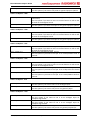
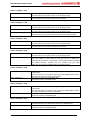
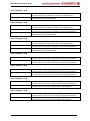
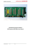
EDP-CM-mbed Adapter Board
mbed ‘Command Module’ – Adapter Board
RS-EDP-CM-mbed User Manual
Version 1.01
29th June 2009
Author: David Giles
Hitex UK Ltd
[email protected]
© Hitex (UK) Ltd. Electrocomponents plc
Page 1
EDP-CM-mbed Adapter Board
Contents
1.0 Introduction
2.0 Solder Link Options
VB – Battery Voltage – J204
DIP Pin 5 Option – J205
DIP Pin 6 Option – J206
DIP Pin 7 Option – J207
DIP Pin 8 Option – J208
DIP Pin 11 Option – J209
DIP Pin 12 Option – J210
DIP Pin 13 Option – J211
DIP Pin 14 Option – J212
DIP Pin 15 Option – J213
DIP Pin 16 Option – J214
DIP Pin 17 Option – J215
DIP Pin 18 Option – J216
DIP Pin 19 Option – J217
DIP Pin 20 Option – J218
DIP Pin 21 Option – J219
DIP Pin 22 Option – J220
DIP Pin 23 Option – J221
DIP Pin 24 Option – J222
DIP Pin 25 Option – J223
DIP Pin 26 Option – J224
DIP Pin 27 Option – J225
DIP Pin 28 Option – J226
DIP Pin 29 Option – J227
DIP Pin 30 Option – J228
3.0 Zero Ohm Links
Vcc_CM - Command Module Voltage – R101
VAGND - Analogue Ground – R102
12VGND – 12V Power Ground – R103
4.0 Software Support
5.0 Schematic Circuit Diagram
6.0 Board Components Layout
© Hitex (UK) Ltd. Electrocomponents plc
Page 2
EDP-CM-mbed Adapter Board
1.0 Introduction
The mbed development module is a very useful board that introduces a new way to write embedded
firmware. Instead of having a C compiler license installed upon your machine the mbed unit makes
use of a C Compiler installed on a virtual host. Your software and project are built within the
framework of an HTML page. The compilation is done remotely on your behalf, and the resulting
binary image file is transferred to you and stored on the mbed module. By rebooting the mbed
module the new image is flashed into the hardware and the mbed module runs your application
code.
This is a superb way of gaining access to complex MCU’s like NXP’s ARM7 based devices without the
requirement to purchase a full blown C compiler and debug tool. The mbed allows for writing of
code, compiling of code and downloading to the target via very simple USB interface. The mbed
platform comes currently as a 40 pin DIP module and software drivers for most of the hardware on
the chip.
This RS-EDP-CM-mbed adapter module is designed to remap the pin out of the mbed module to that
of the RS-EDP platform. The adapter module also includes a mini SD Card interface and an SPI serial
connection for a small graphics LCD.
The RS-EDP platform is a system, which has been designed to utilise many different manufacturers’
microprocessors. To support ARMs mbed module, the RS-EDP platform uses an adapter board to
connect between the RS-EDP baseboard and the mbed module. This is referred to as the EDP-CMmbed module.
The adapter module comes complete with a list of low level drivers that allow it to talk to the other
module that form the RS-EDP system. The applications modules that are currently supported include
analogue module, digital I/O module, communications module, brushed DC motor drive module
MC1. A set of jumper and link options provide the user with several different ways to map the mbed
to the RS-EDP.
In an RS-EDP system there is usually one Command Module (CM) and one or more Applications
Modules (AM) pluged in to the Base Board (BB). This adapter board is designed to hold the mbed
module and as such it will be the ‘Command module’ for the system.
The ‘Command Module’ in a system dictates whether the whole system is a 3.3V one or a 5.0V one.
The module uses a 3.3V microprocessor and consequently the I/O is mostly 3.3V.
To tell the rest of the system the mbed module is a 3.3V Command Module and not a 5.0V Command
Module, the Vcc_CM line on the base board is connected to 3.3V by the tracking on the adapter
board. This Vcc_CM is used as a reference by the other modules, such as the analogue module, to
limit the output voltage to 3.3V. The command voltage line is also used by the #RESET circuit.
The RS-EDP-CM-mbed daughter board remaps the I/O of the mbed module on to the backplane of
the RS-EDP system. As there are quite a few dual function pins on the mbed module several link
options have been made to accommodate the various options. Extensive use of the I2C capability is
used to communicate to the application modules in the system.
© Hitex (UK) Ltd. Electrocomponents plc
Page 3
EDP-CM-mbed Adapter Board
2.0 Solder Link Options
Many of the options for the adapter/daughter board require a solder bridge to be made or a track
bridge to be cut. The adapter board has been designed to be configured in the most popular setting
by using track between the options, which will require cutting with a knife before making the
alternate connection options.
The options we have are as follows:
VB – Battery Voltage – J204
The mbed module has a VB input which is a battery backup voltage supply. You can connected this to
the RS-EDP backup voltage rail or to the standard 3.3V supply via the link option. Note the base
boards are supplied by default without the battery fitted.
J204 – option 1-2
Connects the VB input to the RS-EDP 3.3V main
supply (Default track connection)
Connects the VB input to the RS-EDP 3.3VBAT
supply on the RS-EDP base board.
J204 – option 2-3
DIP Pin 5 Option – J205
J205 – option 1-2
J205 – option 2-3
DIP Pin 5 is connected to CNTRL_SPIMTSR (Default track connection)
Use this option is you want to use it as an SPI function
DIP Pin5 is connected to EVG10_GPIO58
Use this option is you want to use pin 5 as a general purpose I/O line
DIP Pin 6 Option – J206
J206 – option 1-2
J206 – option 2-3
DIP Pin 6 is connected to CNTRL_SPIMRST (Default track connection)
Use this option is you want to use it as an SPI function
DIP Pin6 is connected to EVG9_GPIO57
Use this option is you want to use pin 6 as a general purpose I/O line
DIP Pin 7 Option – J207
J207 – option 1-2
J207 – option 2-3
DIP Pin 7 is connected to CNTRL_SPICLK (Default track connection)
Use this option is you want to use it as an SPI function
DIP Pin 7 is connected to EVG8_GPIO56
Use this option is you want to use pin 7 as a general purpose I/O line
DIP Pin 8 Option – J208
This pin has three functions. It primary function is for use as the chip select pin for the CNTRL SPI.
J208 – option 2-4
J208 – option 2-1
© Hitex (UK) Ltd. Electrocomponents plc
DIP Pin 8 is connected to #CS_LCD (Default track connection)
Use this option is you want to drive an LCD connected to the LCD SPI
connector on the RS-EDP-CM-mbed adapter board.
DIP Pin 8 is connected to CNTRL_SPI_#CD_NSS.
Use this option is you want to use pin 8 as a general purpose chip
select line for the CNTRL SPI. This signal is for possible use by
application modules within the RS-EDP system that want to make use
of the CNTRL SPI bus.
Page 4
EDP-CM-mbed Adapter Board
J208 – option 2-3
DIP Pin 8 is connected to EVG7_GPIO54
Use this option if you want to use pin 8 as a general purpose I/O line
DIP Pin 11 Option – J209
J209 – option 1-2
J209 – option 2-3
DIP Pin 11 is connected to GPIO12_MCICMD(Default track
connection)
Use this option if you want to use it as an SPI function to talk to the
SD Card on the daughter board.
DIP Pin 11 is connected to EVM2_GPIO41_CAPADC
Use this option is you want to use pin 11 as a general purpose I/O line
DIP Pin 12 Option – J210
J210 – option 1-2
J210 – option 2-3
DIP Pin 12 is connected to GPIO2_MCIDAT0(Default track connection)
Use this option if you want to use it as an SPI function to talk to the
SD Card on the daughter board.
DIP Pin 12 is connected to EVM3_GPIO43
Use this option is you want to use pin 12 as a general purpose I/O line
DIP Pin 13 Option – J211
J211 – option 1-2
J211 – option 2-3
DIP Pin 13 is connected to GPIO10_MCICLK (Default track connection)
Use this option if you want to use it as an SPI function to talk to the
SD Card on the daughter board.
DIP Pin 13 is connected to ASC1_TX_TTL
Use this option if you want to use pin 13 as a ASC1/UART1 serial Tx
channel.
DIP Pin 14 Option – J212
J212 – option 2-1
J212 – option 2-4
J212 – option 2-3
DIP Pin 14 is connected to GPIO8_MCIDAT3
Use this option is you want to use it as an SPI function to talk to the
SD Card on the daughter board.
DIP Pin 14 is connected to #CS_SD (Default track connection)
Use this option if you want to use pin 14 as a chip select for the SD
card.
DIP Pin 14 is connected to ASC1_RX_TTL.
Use this option is you want to use pin 14 as a ASC1/UART1 serial Rx
channel.
DIP Pin 15 Option - J213
J213 – option 1-2
J213 – option 2-3
DIP Pin 15 is connected to AN0. (Default track connection)
Use this option if you want to use it as an analogue input.
DIP Pin 15 is connected to EVM0_GPIO21
Use this option if you want to use pin 15 as a general I/O pin.
DIP Pin 16 Option – J214
J214 – option 2-1
J214 – option 2-4
J214 – option 2-3
© Hitex (UK) Ltd. Electrocomponents plc
DIP Pin 16 is connected to AN1.
Use this option if you want to use it as an analogue input on
backplane signal AN1.
DIP Pin 16 is connected to AN10 (Default track connection)
Use this option if you want to use it as an analogue input on
backplane signal AN10.
DIP Pin 16 is connected to EVM1_GPIO23.
Use this option if you want to use pin 16 as a general purpose I/O.
Page 5
EDP-CM-mbed Adapter Board
DIP Pin 17 Option - J215
J215 – option 1-2
J215 – option 2-3
DIP Pin 17 is connected to AN2. (Default track connection)
Use this option if you want to use it as an analogue input.
DIP Pin 17 is connected to IRQ_GPIO16_CNTRL_I2CIN.
Use this option if you want to use pin 17 as a GPIO.
DIP Pin 18 Option – J216
J216 – option 2-1
J216 – option 2-4
J216 – option 2-3
DIP Pin 18 is connected to AN3.
Use this option if you want to use it as an analogue input.
DIP Pin 18 is connected to AN12 (Default track connection)
Use this option if you want to use it as an analogue input.
DIP Pin 18 is connected to CPU_DACO0_GPIO17.
Use this option if you want to use pin 18 as a DAC output or GPIO
DIP Pin 19 Option - J217
J217 – option 1-2
J217 – option 2-3
DIP Pin 19 is connected to AN4. (Default track connection)
Use this option if you want to use it as an analogue input.
DIP Pin 19 is connected to GPIO0.
Use this option if you want to use pin 19 as a GPIO.
DIP Pin 20 Option - J218
J218 – option 1-2
J218 – option 2-3
DIP Pin 20 is connected to AN5. (Default track connection)
Use this option if you want to use it as an analogue input.
DIP Pin 20 is connected to ASC1_RX_TTL_ASCODSR
Use this option if you want to use pin 20 as a GPIO pin.
(Note this pin is used as a chip select on the communications module
for RS422 function enable.) Do not confuse this pin with
ASC1_RX_TTL as this is a different pin on the base board.
DIP Pin 21 Option - J219
J219 – option 1-2
J219 – option 2-3
DIP Pin 21 is connected to CPU_DACO0_GPIO17. (Default track
connection)
Use this function if you want to use this pin for PWM output and for
the signal to appear on this bus connection.
DIP Pin 21 is connected to MOTOR_P0L.
Alternate selection for PWM output.
DIP Pin 22 Option - J220
J220 – option 1-2
J220 – option 2-3
DIP Pin 22 is connected to CPU_DACO1_GPIO19. (Default track
connection)
Use this function if you want to use this pin for PWM output and for
the signal to appear on this bus connection.
DIP Pin 22 is connected to MOTOR_P1L.
Alternate selection for PWM output.
DIP Pin 23 Option - J221
J221 – option 1-2
J221 – option 2-3
© Hitex (UK) Ltd. Electrocomponents plc
DIP Pin 23 is connected to EVG0_GPIO40. (Default track connection)
Use this function if you want to use this pin for PWM output.
DIP Pin 23 is connected to MOTOR_P2L.
Alternate selection for PWM output.
Page 6
EDP-CM-mbed Adapter Board
DIP Pin 24 Option - J222
J222 – option 1-2
J222 – option 2-3
DIP Pin 24 is connected to EVG1_GPIO42. (Default track connection)
Use this function if you want to use this pin for PWM output.
DIP Pin 24 is connected to MOTOR_P0H.
Alternate selection for PWM output.
DIP Pin 25 Option - J223
J223 – option 2-1
J223 – option 2-3
J223 – option 2-4
DIP Pin 25 is connected to EVG2_GPIO44.
Use this function if you want to use this pin for PWM output.
DIP Pin 25 is connected to ASC1_RX_TTL. (Default track connection)
Use this option if you want to use ASC1 for serial communications.
DIP Pin 25 is connected to MOTOR_P1H.
Alternate selection for PWM output.
DIP Pin 26 Option - J224
J224 – option 2-1
J224 – option 2-3
J224 – option 2-4
DIP Pin 26 is connected to EVG3_GPIO46.
Use this function if you want to use this pin for PWM output.
DIP Pin 26 is connected to ASC1_TX_TTL. (Default track connection)
Use this option if you want to use ASC1 for serial communications.
DIP Pin 26 is connected to MOTOR_P2H.
Alternate selection for PWM output.
DIP Pin 27 Option - J225
J225 – option 1-2
J225 – option 2-3
DIP Pin 27 is connected to ASC0_RX_TTL. (Default track connection)
Use this option if you want to use ASC0 for serial communications.
DIP Pin 27 is connected to EVG4_GPIO48.
Use this option if you want to use pin 27 as a general purpose I/O.
DIP Pin 28 Option - J226
J226 – option 1-2
J226 – option 2-3
DIP Pin 28 is connected to ASC0_TX_TTL. (Default track connection)
Use this option if you want to use ASC0 for serial communications.
DIP Pin 28 is connected to EVG5_GPIO50.
Use this option if you want to use pin 28 as a general purpose I/O.
DIP Pin 29 Option - J227
J227 – option 1-2
J227 – option 2-3
DIP Pin 29 is connected to EVM7_GPIO47. (Default track connection)
Use this option if you want to use pin 29 as a general purpose I/O.
DIP Pin 28 is connected to CAN0_TX.
Use this option if you want to use pin 29 for CAN purposes .
DIP Pin 30 Option - J228
J228 – option 1-2
J228 – option 2-3
© Hitex (UK) Ltd. Electrocomponents plc
DIP Pin 30 is connected to EVG6_GPIO52. (Default track connection)
Use this option if you want to use pin 30 as a general purpose I/O.
DIP Pin 30 is connected to CAN0_RX.
Use this option if you want to use pin 30 for CAN purposes .
Page 7
EDP-CM-mbed Adapter Board
3.0 Zero Ohm Links
Vcc_CM - Command Module Voltage – R101
R101 is used to connect the 3.3V rail to the Vcc_CM rail. This Vcc_CM rail is the command module
voltage operating voltage rail. There is only one mbed module at present and it is based on an NXP
3.3V operation MCU. If however a 5V module appears then this link can be removed and replaced
with a wire link to connect the 5V to the Vcc_CM. Under normal circumstance this resistor should
remain fitted and it is the default options.
R101 – option – populated
The Vcc_CM line is connected to 3.3V (DEFAULT)
VAGND - Analogue Ground – R102
The VAGND and SGND lines are connected on the adapter module via the zero ohm link R102. For
different grounding arrangement this resistor may be removed. The main user manual for the RS-EDP
unit explains in more details about the ground options. The analogue module for example can have
its analogue ground line connected to SGND also or instead of at this point.
R102 – option – populated
The VAGND and SGND lines are connected on
the adapter board (DEFAULT)
12VGND – 12V Power Ground – R103
The 12VGND and SGND lines are connected on the adapter module via this zero ohm link R103. The
default setting is to have this removed. See the circuit diagram for the base board module to see how
the grounding scheme for the 12V works.
R103 – option - populated
The 12VGND and the SGND are connected on the
adapter board
The 12VGND and the SGND are not connected on
the adapter board. (DEFAULT)
R103 – option – not populated
4.0 Software Support
The mbed Command Module for the RS-EDP platform is supported by all of the necessary software
drivers to make driving of the platform very easy. All the low level support for the devices controlled
by I2C for example have been written, as well as a test menu to exercise each of the modules
independently of the others. This therefore provides working example of the code which will allow
students and users to cut and paste various sections into their own applications.
Each applications module has its own header file which provides the support for the functions that
control it. Each module has its own set of high level functions that can be called to operate and
control the hardware. This makes life a lot easier for the user, who can then spend most of his time
working at the higher level application layer.
The software has been packed up as a single ZIP file which can be imported into the mbed
development environment by use of the ‘Project- Import’ feature.
© Hitex (UK) Ltd. Electrocomponents plc
Page 8