1
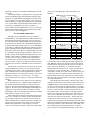
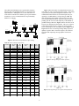
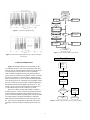
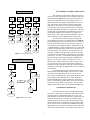
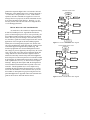
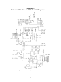
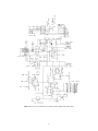
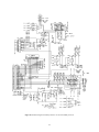
Technical Description
of the
TRAIN CONTROL NETWORK
January 14, 1997
Richard W. Wall
University of Idaho
Department of Electrical Engineering
I.
area. Only the information itself is identified by a 28 bit word
unique to each message type. The message types specified in
SAE standard J1939 assign variables to each data byte in the
message data filed.
Message data lengths are from zero to eight bytes. The
are three instances that initiate network traffic; unsolicited,
request for data, and response to request for data. The unsolicited messages are initiated for system exceptions and by the
server controller as control messages. The server unit request
new data on timed intervals by sending an abbreviated message that contains the message identifier and a single bit that
signals other units on the network that this is a request for
data. Units with this information immediately respond with
the appropriate data message.
All network arbitration and error management is handled
by the CAN controller IC’s either the Intel 82527 or the
87C196CA internal CAN controller. Each CAN transmission
uses bit stuffing for synchronization, 16 bit CRC for error
checking, and message prioritization for collision avoidance.
GENERAL HARDWARE OVERVIEW
Eight processor boards make up the Controller Area Network (CAN); six of which are based on the i80C196CA processor and two on the i87C196KD processor. Software on one
i87C196KD processor board control the DC bus voltage while
the other simulates the track load by controlling the load motors. The program contained on the i87C196CA evaluation
board supports three classes of applications programs; the
server Controller, Inverter Controller, and the Dynamic Brake
Controller. All processor boards have an RS232C serial interface operating at 38.2KB and a CAN interface using the
RS485 physical layer. The applications on the i87C196CA
boards are selected by settings on the eight position DIP
switch. Two sets of DIP LED modules on the i87C196CA
boards provide status information. LED 1 cycles in acknowledgment of accepting a CAN control or status message. LED
2 blinks two elements that identifies the fact that an application program is currently running and another led that identifies which particular application program is executing.
The i87C196CA processor boards are produced by Dearborn Group in Dearborn, MI. The systems are supplied with
Intel RISM (Reduced Instruction Set Monitor) ROMS and
were used while the application programs were under development. There are two possible ways to interface to the CAN
using the 87C196CA evaluation boards; by the external
i87527 CAN controller IC on the PCB or the internal CAN
controller within the 80C196CA processor itself. The
i87C196KD processor boards is produced by Intel and also
supplied with a RISM ROM base monitor. These processor
boards interface with the CAN using an i87527 CAN evaluation board (See appendix B). After development, the RISM
Monitor ROMS, U16 and U17, were replace with application
ROMS programmed with specific code. The address decoding GAL22V10, IC5, on the 87C196CA boards and IC12 on
the 87C196KD boards are modified to permit the system to
operate without a host CPU. The applications code was developed using IAR ICC196 version 5.1 and Codeview IDE
from Chip Tools,. Inc.
The i87C196KD processor boards have the RS232 serial
drivers on the evaluation boards where as the i87C196CA
boards do not. For the later processor boards, the RS232C
drivers are located on an external driver board designed by the
University of Idaho. Each 87C196 processor board and RS232
driver board requires 500ma maximum current at 5 VDC. The
CAN - RS485 serial bus requires a DB9 male connector to
interface to the 87C196CA board.
III. UNIT IDENTIFICATION
Six control units use the 87C196CA processor boards.
All six of these units have the identical microprocessor code.
The boards are set for the particular application by selecting
one of the six S1 DIP switch settings shown in Figure 1. The
switch setting can be set before power is applied and the processor will start in the corresponding applications mode. The
DIP switch settings are only read in the power up initialization
routine. If the switches are modified while the processor is
running, the unit must be reset, either by a power down power up sequence or by pressing the reset push button, S2,
on the processor board. A reset is signaled on the processor
board by all LED’s on LED1 and LED2 flashing three times.
II. CAN MESSAGE STRUCTURE
ON
1
ON
1
ON
1
2
3
4
5
6
7
8
2
3
4
5
6
7
8
2
3
4
5
6
7
8
S1
S1
S1
Master
Traction
Motor
#1
Traction
Motor
#2
ON
1
2
3
4
5
ON
1
2
3
4
5
ON
1
2
3
4
5
6
7
8
6
7
8
6
7
8
S1
S1
S1
Flywheel
#1
Flywheel
#2
Dynamic
Brake
Figure 1. 87C196CA processor board DIP switch settings
The CAN uses a message based communications scheme
that requires no network management resources or time when
nodes enter or exit the network. The primary information
identification comes from a message ID and does not identify
either the source or the destination of the message except by
specific design using fields allocated inside the message data
DIP position 7 of S1 controls the “NO ACTIVITY” automatic reset function. If no commands have been received
from network communications for a period of five seconds.
the unit executes a power up reset. During the reset, the control outputs default to the safe-fail mode and the network is re-
2
initialized to attempt to re-establish communications with the
server unit.
LED indication lights are packaged on two separate LED
clusters each holding eight individual LEDs. During normal
operations, the eight individual LED lights on the LED1 cluster will sequence in a ring counter fashion. For I/O processor
units, the LED’s stop sequencing should network commands
cease. LED number eight on the LED2 cluster flashes at a 4
second rate to signal that the processor is operating. A
second LED on cluster LED2 flashes on at a two second rate.
The particular LED that flashes corresponds to the unit identifier set on S1 as shown in Figure 1.
range of 0 to 1000 although it will be nominally set for
800VDC.
Table I. Server to PC data format
Digit
1
2
3
4
5
6
7
8
9
10
11
12
13
IV. NETWORK OPERATION
Although CAN accommodates peer-to-peer network
communications, this implementation currently has the server
unit managing the network information. Once each second
the server unit requests updated information of all parameters
from other units on the network. This updated information is
communicated with the supervisory PC over a 38.4KB RS232
serial channel. Although using ASCII text characters requires
greater communications time than sending the information as
binary data, ASCII allows data to be qualified quite easily and
is very beneficial during development phases. The PC is expected to operate on this information and generate new commands in a timely manner. When the new commands are received by the server unit, the information is disseminated
over the network as specific messages to be implemented at
remote locations. If there is no response from the supervisory
PC with in one second, no commands are sent out on the network.
Any i80C196CA board can be set to be the server unit by
setting all eight DIP switches on S1 to off and pressing the
reset button on the board. Under normal operation, both LED
units will flash on three times during initialization. Before
beginning operation, a the following text string is sent out the
RS232 port: “%Supervisory system on line”. A carriagereturn / linefeed (CR-LF) sequence is sent before and after the
message.
While running in the server mode, the serial communications to the supervisory PC contains 14 space delimited values using the format shown in Table I. The serial string is
always 69 characters long including the terminating CR-LF
sequence. All values are four decimal digit with leading zero
suppression except for the eleventh value which is a single
decimal digit. The serial communications operates at 38.4KB,
eight data bits, no parity, and one stop bit.
Table II describes the messages from the supervisory PC
to the server controller. Six control variables are passed manage the energy production, use and storage for the train. To
reduce communications overhead, only positive variables are
passed. Present convention uses a range of zero to 2000 as
nominal control parameters. This represents -100.0% to
+999.9% for all converter controls. The DC bus voltage has a
14
Parameter
Traction Motor #1 Torque
Traction Motor #1 Speed
Traction Motor #2 Torque
Traction Motor #2 Speed
Flywheel #1 Torque
Flywheel #1 Speed
Flywheel #2 Torque
Flywheel #2 Speed
DC BUS Volts
DC BUS Amps
Dynamic Brake Control
Train Speed
Train Distance modulo 10K
feet
Train Distance / 10K feet
Range
Min
Max
0
2000
0
2000
0
2000
0
2000
0
2000
0
2000
0
2000
0
2000
0
2000
0
2000
0
1
0
255
0
9999
0
9999
Table II. PC to server data format
Digit
1
2
3
4
5
6
Parameter
Traction Motor #1 Power
Traction Motor #1 Speed
Traction Motor #2 Power
Traction Motor #2 Speed
DC Bus Voltage
Brake control
Range
Min Max
0
0
0
0
0
0
2000
2000
2000
2000
1000
1
The server unit is configured to receive eight different
CAN messages with each message containing eight bytes of
data. Figure 2 illustrates the network configuration and the
message routing. Messages from the server to I/O nodes are
either “request for status data” or “command” messages.
Messages form the I/O units are all “status” messages in response to the “request for status data”. Six units receive
“commands” from the server unit; the two Traction Converter
control units, the two Flywheel Converter control units, the
Dynamic Brake control unit, and the DC bus voltage control
unit. The track position and train velocity data is provided by
the Track Simulator unit.
Table III. describes the message content for each of the
message type used in the system. As the bi-directional arrows
in Figure 2 imply, control messages and status messages between a given unit use the same message number. For example, if the server unit needs an update from the Traction Motor
#1 unit, a “request for data” is made on the network for message number 32769. Traction motor #1 unit then responds
with it’s data using message number 32769. When the server
unit issues a command to Traction Motor #1 unit, it does so
using the same 32769 message number. Another unit monitoring network traffic that in set to receive message 32769
would be able to distinguish the command data from the status
data since the different information occupies different fields in
the message structure as Table III describes. The CMD- STATUS column indicate the information source. As stated
above, the source of command information (C) is the server
3
unit while status information (S) is generated by I/O units.
Message data with unidentified sources are not used in this
implementation. Although the server unit controls the network traffic in a master-slave fashion, peer-to-peer and unsolicited slave to server communications is not precluded by
hardware or software.
Figure 3 shows the order of communications for the network traffic as well as typical information timing. This timing
is specifically for the system designed for RS232C serial
communication between the server and the supervisory PC
operating at 38.4KB and the CAN operating at 74KB. The
delay between the status update to the supervisory PC and
new command data from the PC maybe as long as 150ms depending upon PC activities and complexity of the Matlab algorithm running at that time. Figure 4 shows the effects of an
I/O processor missing from the network. The server waits up
to four milliseconds for after a request for message update
before continuing on to the next update request. Figure 5 and
Figure 6 shows the CAN message timing during request for
updates in greater detail. From these figures, the overhead
associated with requesting message updates can be determined.
IBM Compatible
DC Bus
Controller
Track Simulator
65271
32771
Server
Unit
Flywheel #2
Controller
32772
Flywheel #1
Controller
65256
Traction Motor #1
Controller
65274
32769
32770
CAN Network
65248
Traction Motor #2
Controller
Dynamic Brake
Controller
Figure 2. FRA Network information traffic routing
Table III. Network message data formats
Number
Message
Bit
Message
name
Posidata
tion
32769
-72
Inverter
Torque
Control
Bit 0
Bit 1
Bits 2-3
Bits 4-5
Bits 6-7
65248
Train
Distance
Bits 0-3
Bits 4-7
65256
65271
Train
Speed
Train
Electrical
Direction
Ground Speed
Track Pitch
Track Altitude
Bits 0-1
Bits 2-3
DC Bus Amps
Alternator
Current
Alternator
Volts
Bus Volts
Bits 6-7
Dynamic
Brakes
Trip distance feet
Total Distance
- feet
Bits 0-1
Bits 2-3
Bits 4-5
Bits 6-7
Bits 4-5
65274
Dest. Unit
Source Unit
Unit speed
Commanded
Power
Unit Torque
Bit 0
Bit 1
Bit 2
Bits 3-7
Brake Application
Brake Pressure #1
CMD
Status
Data
Type
S
C
Byte
Byte
Word
Word
S
Word
S
Long
Figure 3. Message timing for normal operations
Long
S
Word
Word
Word
Word
S
Word
Word
C
Word
S
Word
CS
Byt
e
Brake Pressure #2
Byt
e
Byt
e
Unused
NA
Figure 4. Message timing for no response from Flywheel #2
4
Server RTOS
Allocate silicon based
resources
Foreground
token management
Parse String
New line
ready
Yes
Control setpoint
update
Serial Rx ISR
No
Send
network commands
Figure 5. CAN status update message
Yes
Network message
decoded
CAN Rx
message
Control status update
No
Serial Tx
Poll network for
control status
update
CAN Rx
message
Yes
Timer ISR
No
Foreground
token management
Figure 7. server RTOS software flow control
Figure 6. CAN status message update with no response from Flywheel #2 unit
Timer ISR
V. SERVER OPERATIONS
Software
Time
Interrupt
Figures 5 through 1 describe the control flow for the
server RTOS software. Three token generating events determine the activity within the RTOS; an internal software timer,
a CAN message received, and a new line of serial input.
Time-out timers in application processes guarantee that no
process waits for an unanswered request for action or information from any internal or external process. The RTOS loop
must be executed every 15 ms or an internal Watchdog Timer
resets the microprocessor. During the reset (regardless of how
the reset is initiated) resets all control variables an distributes
this initialized information throughout the network. A ‘No
Activity’ flag resets the processor should no messages be received from the supervisory PC within five seconds.
The process called ‘Control Status Update’ in Figure 7
actually consist of a series of request for transmission on the
CAN to update the status data base maintained in the server
processor. This information is posted by the various I/O nodes
in a timely manner such that no information is older than
20ms when the status information is sent to the supervisory
PC. I/O processors transmit data on the CAN only when requested or a control exception is detected by the I/O processor.
Decrement
Time-out Timers
Decrement NO
Activity Timer
Activity in
last 5 Sec?
No
Halt program
without
Watchdog timer
update
Yes
Return to process in
progress
Hardware reset
Figure 8. Timer event generator and 'No Activity' monitor
5
VI. INVERTER CONTROL OPERATIONS
CAN IO
Received
CAN
Message
ISR
Request
CAN
Message
ISR
Qualify
message
Qualify
message
Decode
Message
Identifier
Encode
Message
Identifier
Update Control
Status Buffers
Set CAN Rx
Token
Post CAN
Message
Send CAN
Message
Encode
Message
Identifier
Encode
Message
Identifier
Invallidate
Message
Invallidate
Message
Set CAN
control for TX
Reqest
Move control
data to CAN
message area
Move control
data to CAN
message area
Process
complete
Set CAN
control for
new data
Set CAN
control for
new data
Vallidate
Message
Vallidate
Message
Process
complete
Process
complete
The operations of the inverter control processors except for the message ID number used for passing control and
status information. Figure 11 describes the control flow for
the inverter unit RTOS software. The support routines are
identical to Figures 8 through 10 implemented in the server
unit. This feature makes efficient code development and
maintenance. There are two events that cause an updated
CAN message to be posted; New information received from
the serial input and the expiration of a 10ms timer. The inverter DSP units are programmed to automatically reply the torque and shaft angular velocity data after receiving a command. Hence, when a timer generated command is sent, the
status information is also updated because of this action.
The four inverter control messages (message ID
32769 through 32772) have five fields as shown in Table II.
The Destination and Source Node ID fields are a reference to
previous generations of network code and are no longer actively used for present implementations. Information for the
“Commanded Power’ field is supplied by the server unit using
a data base maintained locally on the server unit. Before the
control message is sent, data last received from the inverter
controller is filled into the appropriate fields in the message.
This data base is maintained by communications with the supervisory PC. Inverter - CAN interface units supply the data
for the unit torque and unit speed using an 38.4KB RS232
interface. Inverter power data received from the server is
filled into the CAN message before being sent by the inverter-CAN interface units. This in effect makes complete information messages regardless of the source node and allows
convenient monitoring by an independent processor connected
to the network,
Specifically, the 80C196CA unit sends the inverter
DSP unit a ASCII decimal number in the range of 0 to 2000
which the inverted DSP interprets as -100.0% to +99.9%.
This string is terminated with a conventional ASCII line-feed
and a carriage-return (0DH and 0AH). Since the MCS96
Evaluation PCB does not support an RS232C serial port directly, a Serial Interface and I/O Driver board was developed
by the University of Idaho for this purpose. The schematic
diagram of this PCB is shown in the appendix as Figure 15.
Figure 9. CAN message control
SERIAL IO
Serial Output
(printf - putch
-puts)
Serial Input
(gets - getch
- new line)
Yes
Buffer
full?
Serial
Input ISR
No
Load
transmit
ring
buffer
Initiate Tx
ISR
Initiate Tx
ISR
Yes
Char ==
\n or \r?
No
VII. BRAKE CONTROLLER
Load
receive
ring
buffer
The RTOS software flow control described by Figure 12 uses support routines identical to those shown in Figures 8 through 10 as implemented in the server unit. The
main difference between the this 80C106CA application code
and those discussed above is that the I/O is directly implemented on the microprocessor board using the add-on serial
interface and I/O driver board shown in the appendix as Figure 2. The I/O driver circuit has been modified to allow the
digital tachometer to monitor an auxiliary contact on the brake
unit for brake position status. The microprocessor unit is pro-
Return to RTOS
process manager
Figure 10. Serial IO control
6
INVERTER CONTROL RTOS
grammed to output the digital value over both the CAN and
the RS232C serial channel when a new position is detected; a
‘1’ if the brake is energized and ‘0’ if not.. Under normal
operation, the brake commands are supplied via a network
messages but for test purposes, the brake commands can also
be set using the RS232 serial interface. Entering a ‘1’ followed by a return will cause the brake to be energized and a
‘0’ will disengage the brake.
Allocate silicon based
resources
Foreground
token management
Parse String
New line
ready
Yes
Post
network message
No
CAN Rx
message
YES
Serial Tx
control data
VIII. DC BUS VOLTAGE CONTROLLER
As stated above, this controller is implemented using
an Intel i87C196KD processor. Appendix B describes the
process of interfacing this processor or, more specifically, the
i87C196KD Evaluation board to the i82527 CAN evaluation
board. Since the processors belong to the same family of micro controllers, significant code developed for the i87C196CA
applications was leveraged for the i87C196KD programs.
Namely the CAN management programs were useable with
only minor modifications which dealt with the CAN processor
reset and the physical mapped memory addressing. The
closed loop algorithm uses conventional digital PI control.
The voltage set point is supplied by the supervisory PC via the
CAN. The on-chip 10 bit AD converter digitizes the DC bus
voltage and DC bus current transducers signals which are
needed for closed loop control and system status. Figure 13
shows that process control loop the DC bus controller includes
an LCD display of instrumentation and control variables. The
LCD is updated once for every 15 AD conversion complete
interrupts. During the AD complete ISR, the PI algorithm is
executed and the instrumentation data is posted to the CAN
controller. The PI algorithm uses a 10 ms sample rate by
scheduling the PTS (Peripheral Transaction Server) to burst
convert two AD channels. At the end of the burst cycle, the
i87C196KD is interrupted to begin processing the AD complete ISR. Figure 16 in Appendix I shows the schematic diagram for the IO driver and LCD interface board.
Serial Rx ISR
Network message
decoded
No
CAN Rx
message
YES
Timer ISR
Serial Tx
control data
No
Post
network message
Foreground
token management
Figure 11. Inverter control RTOS flow diagram
DYNAMIC BRAKECONTROL RTOS
Allocate silicon based
resources
Foreground
token management
Parse String
Post
network message
YES
Yes
New line
ready
Serial Rx ISR
No
CAN Rx
message
Network message
decoded
Set digital output
Read digital input
No
Serial Tx
control data
YES
CAN Rx
message
Timer ISR
Set digital output
Read digital input
No
Post
network message
Foreground
token management
Figure 12. Brake controller RTOS flow diagram
7
Figure 13. DC bus control and instrumentation unit flow diagram
DC BUS VOLTAGE CONTROLLER
Allocate silicon based
resources
Foreground
token management
Compute new
control output
Yes
Post instrumented
data to CAN
PID Loop
Control
AD Complete ISR
No
Schedule next AD
sample
Update LCD and
reset loop counter
Yes
AD loop
counter
AD Complete Flag
No
Register VDC Set
Point
Relay VDC S.P.,
VDC Inst., & IDC
Inst. to RS232 port
Yes
CAN Rx
message
Network message
decoded
No
Send RS232C
Serial Data
Foreground
token management
8
TRACK-LOAD SIMULATOR
Allocate silicon based
resources
Foreground
token management
Determine Speed
and Distance
Traveled
Yes
Simulator
algorithm
AD Complete ISR
Determine Load
torque
No
Post instrumented
data to CAN
Schedule next AD
sample
Update LCD and
reset loop counter
Yes
AD loop
counter
AD Complete Flag
Register VDC Set
Point
Relay speed and
distance data to
RS232 port
No
Send RS232C
Serial Data
Foreground
token management
Figure 14. Track-Load simulator flow diagram
9
Appendix I
Driver and Interface Board Schematic Diagrams
Figure 15. 87C196CA I/0 auxiliary driver board schematic diagram
10
Figure 16. 87C196CA I/0 auxiliary driver board schematic diagram for brake control
11
Figure 16 Schematic diagram of auxiliary IO driver for the 87C196KD processors
12
Appendix II
Notes on Interfacing the Intel 82527 CAN controller satellite board to the 87C196KD-20
Evaluation Board
A.II.I. Introduction
The following discussion addresses issues interfacing the Intel CAN controller satellite board with a 87C196KD-20
Evaluation board. It was determined through research and experimentation that some hardware modifications are necessary.
These modifications are concentrated in three areas. The 60 pin DIN connector, JP3, the addressing mapping PAL, U12, and
the 87C196KD crystal, X1. No modifications of the 82527 CAN satellite board were necessary but jumper settings must be set
for 8 bit standard Intel data transfers.
Code has been developed using ICC196 by IAR Systems[1] C compiler version 5.10 and 80196 assembler. This code
was loaded onto the 80C196 Evaluation board Rev. 3.1 running KBRISM Rev.1.2[2] using Chip-View 196 version 1.33 by
ChipTools[3].
The EV82527 Rev. 1.1 evaluation CAN satellite board is available from Dearborn Group[4]. Reference manuals the evaluation boards[5,6,7] were needed to design and trouble shoot hardware modifications.
A.II.II. EV80C196KD-20 JP3 Modifications
Interfacing the two evaluation boards is accomplished by connection the 60 pin header JP3 on the component side of
the EV87C196KD-20 to 72 pin connector, JP4 on the solder side of the EV82527. Only Pins 1 through 60 of JP4 on the
EV82527 board are necessary and there is direct correspondence in pin functionality if the EV82527 mounts directly over the
EV87C196KD-20 board. Since the “ON-CHIP UART” connector, P2, interferes with JP4 on the EV82527 board, it is necessary to extend the pins of JP3 on the EV87C196KD-20 board in some manner. In this particular case, the pin header was removed from JP3 of the EV80C196KD-20 board and was replaced with a pin header with 0.75 inch long pins. This provided
approximately 0.25 inches of clearance between P2 of the EV80C196KD-20 board and JP4 of the EV82527 board. Note: using a ribbon wire with two connectors will not correct as doing so will reverse the odd and even pin locations.
A.II.III. EV80C196KD-20 U12 PAL Modifications
The function of GAL22V10 (U12) PAL on the EV80C196KD-20 board is to provide chip selects for the EPROM and
RAM memory, the 82510 UART IC as well as buswidth control and generate wait states for the 87C196KD processor. The
logic equations for this PAL are listed in the EV80C196KD user’s manual[2]. The design equations have been converted for
use with ISP Synario[8]distributed by Lattice Semiconductor who also manufactures the GAL22V10 programmable logic device (PLD). An Intel application note[9] provides used information when designing the modified PLD for interfacing the a 20
Mhz 8XC196 processor to the 82527. The PLD must be modified to set the 87C196KD into 8 bit buswidth mode and generate
three wait states for mapped memory accesses to the 82527 CAN controller in the memory address range of 0CA00 through
0CCFFH. The Address decoding PAL (U3) on the EV82527 is programmed for an 82527 chip select in address space
0CA00H through 0CAFFH. U3 also asserts the 82527 reset pin low when a “byte write” (8 bit memory write) is made to any
address in the range 0CB00H through 0CBFFH. The 82527 reset is released (set high) when a “byte write” is made to any
address in the range 0CC00H through 0CCFFH. U3 does not need to be modified for this interface strategy. The modified
PLD code is provided in Appendix I.
A.II.IV. EV80C196KD-20 CRYSTAL, X1 Modifications
Although the Intel application note[9] discusses many issues with interfacing an 82527 CAN controller with a 20 Mhz
8X196 processor, it was found the EV87C196KD-20 board design is insufficient to support 20 Mhz operation. By experimentation, it was determined that changing the 87C196KD processor crystal, X1, to a frequency less than 18.5 Mhz but greater
than 8 Mhz would result in proper operation. It was determined that the EV82527 board provided sufficient loading at 20
Mhz to render the EV80C196KD-20 inoperative even all IC connecting to the address, data and processor handshaking lines.
13
A.II.V. EV82527 JUMPER SETTINGS
The 82527 CAN controller allows for 8 to 16 bit data bus and for handshaking which is common to either Intel or
Motorola processors. Intel processors use separate active low read and write controls. Motorola processors use and active
low enable or select controls and a read-write control. The read-write control is asserted high for a processor read and is asserted low for a processor write. The following jumper setting configures the EV82527 for standard Intel 8 bit mode using the
on-board 16 Mhz crystal.
E0
E1
E2
E4
E5
E6
JP6-1 2 Open
JP6-3 4 Open
JP6-5 6 Open
JP6-7 8 Open
JP6-9 10
JP6-11 12
JP6-13 14
JP6-15 16
A-B Shorted
A-B Shorted
A-B Open
A-B Shorted
A-B Shorted
A-B Shorted
Open
Open
Open
Open
V. REFERENCES
[1] IAR Systems, Internet: support.iar.com, Tel: 415-765-5500, FAX: 415-765-5503
[2] EV80C196KD Evaluation Board User’s Manual, Release 001, May 8 1992, Intel Corp., Order Number: 27193-001
[3] ChipTools, 1232 Stavebank Road, Mississauga, Ontario, Canada, L5G2V2, Internet: [email protected], Web:
www.chiptools.com, Tel: 905-274-6244, FAX: 905.891.2715
[4] Deargorn Group, Inc., 37632 Hills Tech Drive, Tel: 810 488-20082
[5] 8XC196KC/KD User’s Manual, 1992, Intel Corp. Order Number: 272238-001
[6] 82725 Serial Communications Controller Architectural Overview, 1993, Intel Corp., Order Number: 272410-001
[8] ISP Synario Starter Software & ISP Encyclopedia, CD, July 1996, Lattice Semiconductor Corp. 5555 Northeast Moore
Court. Hillsboro, OR, 97124, Tel: (503) 681-0118, FAX:(503) 681-3037.
[9] Interfacing a 20 Mhz 8XC196 to an 82527 Serial Communications Controller, John Shill, August 1995, Intel Corp., Order
Number: 272732-001
14
Appendix III
Modified PLD code for EV80C196KD-20 U12.
MODULE KD-CAN
TITLE 'KD-RISM PAL for 82527 interface'
"U12 device 'p22v10';
"Constants
H, L, X, Z, C = 1, 0, .X., .Z., .C.;
"Inputs
CLKOUT
STALE
!HLDA
A15, A14, A13, A12
A11, A10, A9, A8
!RESET
"Outputs
MAP
!CE1
!CE0
!WAIT
SB2
SB1
SB0
!BUSWIDTH
!CE2
!CS510
pin 1;
pin 2;
pin 3;
pin 11, 10, 9, 8;
pin 7, 6, 5, 4;
pin 13;
pin 23 ISTYPE 'reg, pos, buffer' ;
pin 22;
pin 21;
pin 19;
pin 20 ISTYPE 'reg, pos, buffer' ;
pin 18 ISTYPE 'reg, pos, buffer' ;
pin 17 ISTYPE 'reg, pos, buffer' ;
pin 16;
pin 15;
pin 14;
MEMADDR
= [A15, A14, A13, A12, A11, A10, A9, A8, X, X, X, X, X, X, X, X];
EPROM
=
EEPROM
=
((MEMADDR>=^h6000) & (MEMADDR<=^h7FFF));
RAM
=
(MAP & ((MEMADDR >=^h2000) & (MEMADDR<=^h27FF))) #
(MEMADDR >=^h2800) & (MEMADDR<=^h5FFF);
OPEN0
=
((MEMADDR>=^h100) & (MEMADDR<=^h1CFF));
OPEN1
=
((MEMADDR>=^h8000) & (MEMADDR<=^hBFFF));
OPEN2
=
((MEMADDR>=^hD000) & (MEMADDR<=^hFFFF));
CAN
=
((MEMADDR>=^hC000) & (MEMADDR<=^hCFFF));
UART
=
((MEMADDR>=^h1E00) & (MEMADDR<=^h1EFF));
bw
=
EEPROM # UART # CAN;
SR
=
[SB2, SB1, SB0];
ASYNC_START
HOLD2
=
HOLD3
=
HOLD4
=
HOLD5
=
!MAP & ((MEMADDR>=^h2000) & (MEMADDR<=^h27FF)) #
((MEMADDR>=^h0) & (MEMADDR<=^hFF)) #
((MEMADDR>=^h1D00) & (MEMADDR<=^h1DFF));
=
[ 0, 0, 0];
[ 0, 0, 1];
[ 0, 1, 1];
[ 1, 1, 1];
[ 1, 1, 0];
15
HOLD6
=
[ 1, 0, 0];
HOLD7
=
[ 1, 0, 1];
REMOVE_HOLD =
[ 0, 1, 0];
WAIT7
WAIT6
WAIT5
WAIT4
WAIT3
WAIT2
WAIT1
=
=
=
=
=
=
=
0;
WAIT7;
WAIT6;
WAIT5;
STALE & !HLDA & (WAIT4 # CAN);
STALE & !HLDA & (WAIT3 # UART);
STALE & !HLDA & (WAIT2 # EPROM # OPEN0 # OPEN1);
equations
CE0 =
EPROM;
CE1 =
RAM;
CE2 =
EEPROM;
CS510
=
UART;
BUSWIDTH =
bw;
MAP.D
MAP.AR
MAP.SP
MAP.OE
=
=
=
=
MAP # (!STALE & ((MEMADDR>=^h1000) & (MEMADDR<=^h1DFF)));
RESET;
0;
1;
SB0.AR
SB0.SP
SB0.OE
SB1.AR
SB1.SP
SB1.OE
SB2.AR
SB2.SP
SB2.OE
= RESET;
= 0;
= 1;
= RESET;
= 0;
= 1;
= RESET;
= 0;
= 1;
state_diagram SR;
state ASYNC_START:
WAIT = WAIT1;
case
WAIT1 & !WAIT2 : REMOVE_HOLD;
WAIT2
: HOLD2;
!WAIT1 & !WAIT2 : ASYNC_START;
endcase;
state HOLD2:
WAIT = 1;
if WAIT3 then HOLD3 else REMOVE_HOLD;
state HOLD3:
WAIT = 1;
if WAIT4 then HOLD4 else REMOVE_HOLD;
state HOLD4:
WAIT = 1;
if WAIT5 then HOLD5 else REMOVE_HOLD;
state HOLD5:
16
WAIT = 1;
if WAIT6 then HOLD6 else REMOVE_HOLD;
state HOLD6:
WAIT = 1;
if WAIT7 then HOLD7 else REMOVE_HOLD;
state HOLD7:
WAIT = 1;
goto REMOVE_HOLD;
state REMOVE_HOLD:
goto ASYNC_START;
END KD-CAN
17