1
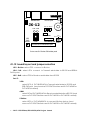
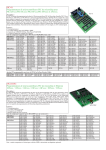
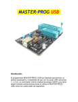
JX-12 PIC12F629/675, PIC16F630/676 Project board l On-Board PIC12F675 , can use with PIC16F630/676 l 2.00”x3.25” Prototype area with 594 pads l Downloading of program via PC parallel port l Selection of RUN/PROG mode by switch l Built in RS-232 interface and iButton socket l Requires Power DC adapter 16V 500mA l Comes with PC Cable, CD (Win98SE/ME/XP) and User Manual JX-12 : PIC12F6xx/PIC16F630/676 Project board 1 9-12V ON SERIAL DATA DOWNLOAD JX-12 +5V Sout GND RS-232 port RxD TxD iButton RUN PGM iButton GP5 GP4 GP2 PIC12F675 GP3 RA3 RESET MODE RxD iButton TxD PIC16F630/676 PIC12F675's & PIC16F676 port 5 4 3 Port C Proto area 3x2 Inches 594 solder pads JX-12 board layout and jumper selection GP2 : iButton select GP2 connect to iButton GP4 : TxD - select GP4 connect to Transmit serial data to RS-232 and SERIAL DATA point GP5 : RxD - select GP5 to Receive serial data from RS-232 Port C : 3-TxD select RC3 of PIC16F630/676 to Transmit serial data to RS-232 and SER-OUTpoint (must remove PIC12F675 before and fit PIC16F630 or PIC16F676 instead) 4-RxD select RC4 of PIC16F630/676 to Receive serial data from RS-232 (must remove PIC12F675 before and fit PIC16F630 or PIC16F676 instead) 5-iButton select RC5 of PIC16F630/676 to connect iButton device (must remove PIC12F675 before and fit PIC16F630 or PIC16F676 instead) 2 JX-12 : PIC12F6xx/PIC16F630/676 Project board Figure 1 : JX-12 project board schematic JX-12 : PIC12F6xx/PIC16F630/676 Project board 3 K1 +VBATT IC3/2 2 3 R8 4k7 9 R5 10k R3 10k +5V IC3/4 R4 4k7 7 4 D1-D4 1N4001x4 R1 10k S1 RESET/GP3/RA3 8 +5V IC3/3 5 6 R6 10k 5 IC3/1-IC3/5 74LS07 10 GND D3 ACK D0 D1 IC3/1 14 2 1 3 K2 PARALLEL PORT RJ11-6P6C +5V J1 DC 9-12V S1 ON/OFF +Vpp Q1 BC557 R2 10k +5V C8 0.1/50V C1 220/25V LED1 RUN R7 510 C2 0.1/50V IC1 7805 C3 10/50V LED2 PGM +5V 7 14 1 4 11 12 C11 33pF +5V 4 6 7 13 8 IC2 MAX662 C10 0.1/50V 5 2 1 * Optional S2 MODE C4 0.1/50V C5 0.22/50V RA1/AN1/CLK 2 OSC_IN X1 4MHz 5 8 1 RA2 RA0 RA1 +5V C9 0.1/50V GP5 GP4 GP2 GP1 GP0 RC3 3 RA4/ OSC_OUT RC0/AN4 RC1/AN5 RC0 RC1 RC2 C12 33pF 10 9 8 JP6 RC3 SELECT JP5 RC4 SELECT 7 RC3 RC5 JP4 RC5 SELECT 6 RC4 RC4 RC5 IC5* RC2/AN6 PIC16F676 RA3/MCLR/Vpp RA2/AN2 5 GP5/OSC1/ 2 T1CKIN/CLKIN RA0/AN0/DATA MCLR/GP3 GP2 +Vpp 12V GP4/OSC2/ 3 T1G/CLKOUT IC4 PIC12F675 GP1/CLK C7 4.7/50V C6 0.22/50V GP0/DATA 6 4 3 TxD iButton RxD TxD Sout JP3 GP5 SELECT RxD JP2 GP4 SELECT iButton JP1 GP2 SELECT R9 2.2k +5V 5 4 IC6 ICL232 R10 220 15 2 6 +5V 3 4 5 1 2 7 8 6 K6 SERIAL PORT +5V SERIAL DATA GND C15 10/50V C16 10/50V 13 14 3 1 C14 10/50V 16 C13 +5V 10/50V SK1 iButton RA2 K7 RA1 SERIAL OUT RA0 CLK_OUT RC5 K4 RC4 PIC16F676 Port RC3 RC2 RC1 RC0 12 11 C17 10/50V GP0 GP1 GP2 GP4 GP5 K3 PIC12F675 Port Using JX-12 board Preparation Before using, user must prepare some tool and software following : 1. Personal computer which install Window 95/98/ME/2000/XP, text editor program, MPLAB, MPASM and Miracle-PIC software MPLAB and MPASM are licenced by Microchip Technology , for more information please contact at http://www.microchip.com (included in CD-ROM when order JX-877 board) Miracle-PIC is licenced by Innovative Experiment Co.Ltd. Please contact at www.inex.co.th (included in CD-ROM when order JX-876 board) 2. Write program, set beginning address at 0x0000 and save file in .ASM 3. Assembler .ASM file by MPASM with selected INHX8M type. So it will be HEX file 4. Prepare DC adpator 16-20V 500mA. Procedure 1. Constuct the curcuit, solder the components on prototype area on JX-628 2. Connect JX-628 with PC’s parallel port. 3. Supply voltage to JX-628 board, green LED at “RUN” mode is bright. 4. Press MODE switch for changing to PROGRAM mode, red LED is bright. 5. Open mPicFlash.EXE (after install Miracle PIC flash software) 6. Select PIC16F628 or PIC16F628A microcontroller. 7. Open HEX file. 8. Erase data in microcontroller by pressed 9. Check blank data in microcontroller by pressed 10. Program data in microcontroller by pressed 11. Check the result by pressed and notice 12. In case, protect data.Select code protection in View à Configuration. PIC16F628 can choose 4 protection types; CP All, 0200H-07FFH,0400H-07FFH and CP OFF. These protection types have to choose before prigramming. Moreover, users can protect data from EEPROM by select CPD in Configuration. 13. After programming completed, press MODE switch to RUN mode. Microcontroller will runs your own program. 14. Save in desk, have to code protect. User can check by put microcontroller in socket, open Miracle-PIC program after that, press READ then select View menu à Program buffer and Data buffer.If showing 000, means code protect. After read data, select File menu à Save file As and name file.HEX 4 JX-12 : PIC12F6xx/PIC16F630/676 Project board Using Miracle-PIC programmer software Menu Control button Select microcontroller Clock mode Auto detect button Protection type Microcontroller type Operation status Show microcontroller ID Show MCU’s configuration word Figure 2 : Miracle-PIC Flash software main window Main Control Button Open Miracle PIC-Flash program, then select the microcontroller as figure 2, there is 8 function buttons follow this; Open : Open HEX file Save : Save source code in HEX file PROGRAM : Program all data into program memory and EEPROM VERIFY : Test program; compare data in buffer with MCU’s data READ : Read data from selected microcontroller and also read parameter BLANK CHECK : Check blank data inside microcontroller ERASE : Delete data in program memory of selected microcontroller. This function used with flash microcontroller memory or EEPROM only. For example, PIC16C84 or PIC 16Fxxx Select microcontroller : Just click at the arrow. User will see many MCU lising. JX-12 : PIC12F6xx/PIC16F630/676 Project board 5 Menu description File Open file - To open file.HEX Save file As - To save data in another file name Recent files - To open recently file Exit - Quit View To see all parameter of PIC microcontroller Program Buffer (F11) - shows code in program memory (figure 3). User can edit by select memory position and input value directly or use Fill Progran Bufer Function Data Buffer (F12) - shows all data EEPROM (figure 4). User can edit data by select memory position and input value directly or use Fill Progran Buffer Function Configuration (F9) or disable all parameter. - shows detail of PIC configuration. User can enable Calibrating OSCCAL - select to calibrate oscillator frequency internal PIC12F675/PIC16F630/676 in case select INTRC operation mode Count Program use this function in JX-628) Stay on top - show number of programmed microcontroller (not - Make the program always on the top Figure 3 : Program buffer window, user can see all code and edit any address 6 JX-12 : PIC12F6xx/PIC16F630/676 Project board Figure 4 : Data buffer window, user can see all data in EEPROM within microcontroller and edit any address Figure 5 : Configuration window Configuration Setting Before programing PIC microcontroller, always fix configuraruon, go to View à Configuration. This is detail of them. Oscillator - select clock mode, there are 8 types LP - low cystal (normally not use in JX-12) XT - normal cystal not over 4 MHz (normally not use in JX-12 in case fit PIC12F675 but use this mode in case fit PIC16F630 or PIC16F676 on JX-12 board ) HS - Over 4 MHz high frequency xtal (normally not use in JX-12) EXTCLK - External Clock (not use in JX-12) INTRC - Internal RC circuit EXTRC (ER) - External RC circuit (not use in JX-12) INTRC clockout - Internal RC circuit and send fOSC/4 clock signal out OSC2 pin. User can select OSC2 pin to RA6 port pin or Clock out pin t (not use in JX12) EXTRC clockout - External RC circuit and send fOSC/4 clock out OSC2 pin. User can select OSC2 pin to RA6 port pin or Clock out pin t (not use in JX-12) Code protection - Use for selceting protection mode, ON or OFF. Select CPD box for protection data in EEPROM. Configuration - To select special ability of PIC miocrocontroller, it depends on type of microcontroller. For PIC12Fxxx has 4 types; WDTEN (watchdog Timer) PWRTEN (Power-up Timer) MCLR (Master ClearReset) : for select MCLR function to RESET. If not select, this pin assigned to RA5 input port pin. BODEN (Brown-out Reset) JX-12 : PIC12F6xx/PIC16F630/676 Project board 7 Device Select type of PIC microcontroller Command Arrange reading, writing and testing data in microcontroller memory Program Chip (F4) - Program code and data to microcontroller as PROGRAM buttom Verify Chip (F5) - Check writing data in PIC microcontroller correct or incorrect as VERIFY buttom Read Chip (F6) - Read data from microcontroller as READ buttom Erase Chip (F7) - Delete data in PIC microconrtoller as ERASE buttom Blank Chip (F8) as BLANK CHECK button - Check blank data in PIC microcontroller memory Option Separate 4 parts; Part1 Program/Verify Program - check latest programming in microcontroller with buffer. Program/Verify Data latest programming - check data in microcontroller memory after Program/Verify ID - checking ID value in microcontroller after latest programming (not use in JX-12) Program/Verify Configuration - check configuration value after latest programming Part2 Special feature in Miracle-PIC programmer software Verfy while program - check data while program microcontroller. If occur the faults, program will stop in suddenly. Auto verify after program - check data after completely programming automatic. Auto erase before program - delete data before programming Program all address - program data in every address Part3 Configuration erase message - selcet warning window Part4 Parallel port 8 JX-12 - select parallel port LPT1 to LPT3 : PIC12F6xx/PIC16F630/676 Project board