1
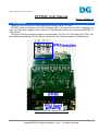
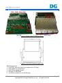
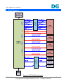
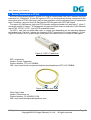
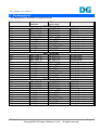
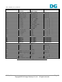
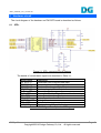
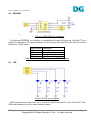
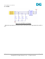
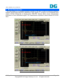
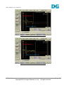
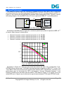
AB15_SFPFMC_user_manual.doc
SFPFMC User Manual
Rev1.0 15-May-14
1 Introduction
Thank you for choosing SFPFMC board [Part Number: AB15-SFPFMC].
SFPFMC board is compliant with FMC standard (HPC) and provides four SFP+ channels, so
user can build and evaluate multi-channel 10-Gb Ethernet system by connecting SFPFMC to
FPGA board.
The board includes voltage-translator to support both 1.8V and 2.5V interface with FPGA. Low
jitter differential oscillator at 312.5 MHz is mounted on the board to support 10-Gb Ethernet.
Figure 1-1 SFPFMC Board Connection
15-May-14
Page 1
Copyright©2014 Design Gateway Co,.Ltd.
All rights reserved.
AB15_SFPFMC_user_manual.doc
2 Board Appearance
Figure 2-1 Both views of SFPFMC Board
Figure 2-2 SFPFMC board size (mm unit)
Board specification
1. 4-ch SFP+ connector which can support up to 10 Gbps
2. 4-bit DIPSW for general input
3. 4-bit LED for general output
4. 256-byte I2C EEPROM
5. 312.5 MHz oscillator for 10-Gb Ethernet
15-May-14
Page 2
Copyright©2014 Design Gateway Co,.Ltd.
All rights reserved.
AB15_SFPFMC_user_manual.doc
Voltage
Translator
Voltage
Translator
Data3
Control/
Control/
Control/
Status3 Data2 Status2 Data1 Status1
Data0
Control/
Status0
3 Block Diagram
Figure 3-1 SFPFMC Block Diagram
15-May-14
Page 3
Copyright©2014 Design Gateway Co,.Ltd.
All rights reserved.
AB15_SFPFMC_user_manual.doc
The interface between FMC-HPC and SFP+ connector can be split into two groups, i.e.
control/status and data. The control/status signals are connected through voltage translator for
compatible to many voltage levels of FMC on each FPGA board. The data differential signals are
direct connected to transceiver pin of FPGA. There are four channel of SFP+ connector available
on the board. The signals of each SFP+ are independent controlled.
Refer to “SFF-8431 Specification Rev 4.1”, the description of each control/status signals are
follows.
Signal
Name
TxFault
TxDisable
RS0
ModABS
RxLos
Dir
Description
Out Assert high to indicate that the module transmitter has detected a fault
condition related to laser operation or safety.
In
Assert high to turn off the module transmitter output. Pull-down resistor is
assembly on the board to force low value as default value.
In
Rate selection input. Set ‘1’ to support 10-Gb Ethernet.
Out Assert high when the SFP+ module is physically absent from a slot.
Out Assert high to indicate an optical signal level below that specified in the
relevant standard.
Table 3-1 SFP+ Control/Status signal description
Otherwise, the interface of 256-byte I2C EEPROM, 4 LEDs, and IPLock are also connected
through voltage translator while 4-bit DIPSW are direct connected.
15-May-14
Page 4
Copyright©2014 Design Gateway Co,.Ltd.
All rights reserved.
AB15_SFPFMC_user_manual.doc
4 Board Connection to FPGA
SFPFMC board supports both 1.8V and 2.5V I/Os to communicate FMC-HPC interface on Xilinx
evaluation kit. Differential TX and RX signal of SFP+ on the board are directly connected to the
transceiver pins of FPGA. Moreover, the low-jitter oscillator is fed to reference clock of transceiver
bank. Therefore, user can build 10-Gb Ethernet FPGA system with SFPFMC board.
To support 10-Gb Ethernet, high-end FPGA model must be selected such as Kintex-7, Virtex-7,
and some model of Virtex-6. The examples of supported Xilinx board to evaluate 10-Gb Ethernet
are KC705, ZC706, VC707, and VC709 evaluation board.
For SFP+, user can use either fiber optic or copper type depending on the operating distance
and budget cost. Figure 4-1 shows the example of SFP+ transceiver for longer distance (10 km).
Figure 4-2 shows LC-LC duplex single mode patch cord which uses to connect to fiber spool.
Figure 4-1 SFP+ Transceiver
SFP+ transceiver
Vendor: Finisar Coperation
Product Number: FTLX1471D3BNL
URL: http://www.finisar.com/products/optical-modules/sfp-plus/FTLX1471D3BNL
Figure 4-2 Fiber optic cable
Fiber Optic Cable
Vendor: Fibertronics Inc
Product Number: PC-KK9D3YV01M
URL: http://www.fiberopticcableproducts.com/
15-May-14
Page 5
Copyright©2014 Design Gateway Co,.Ltd.
All rights reserved.
AB15_SFPFMC_user_manual.doc
5 Pin Assignment
Pin assignment of SFPFMC is listed as follows.
FMC HPC Pin#
FMC
definition
A30
A31
A10
A11
D21
D20
G18
G19
H20
H19
C19
DP3_C2M_P
DP3_C2M_N
DP3_M2C_P
DP3_M2C_N
LA17_N_CC
LA17_P_CC
LA16_P
LA16_N
LA15_N
LA15_P
LA14_N
A26
A27
A6
A7
C18
D18
G16
D17
G15
H17
H16
DP2_C2M_P
DP2_C2M_N
DP2_M2C_P
DP2_M2C_N
LA14_P
LA13_N
LA12_N
LA13_P
LA12_P
LA11_N
LA11_P
A22
A23
A2
A3
C15
C14
D14
D15
G13
G12
H14
DP1_C2M_P
DP1_C2M_N
DP1_M2C_P
DP1_M2C_N
LA10_N
LA10_P
LA09_P
LA09_N
LA08_N
LA08_P
LA07_N
SFP Board
signal name
SFP+ Channel#0
TD_SFP0_P
TD_SFP0_N
RD_SFP0_P
RD_SFP0_N
TxFault_SFP0
TxDis_SFP0
SCL_SFP0
SDA_SFP0
MODABS_SFP0
RS0_SFP0
LOS_SFP0
SFP+ Channel#1
TD_SFP1_P
TD_SFP1_N
RD_SFP1_P
RD_SFP1_N
TxFault_SFP1
TxDis_SFP1
SCL_SFP1
SDA_SFP1
MODABS_SFP1
RS0_SFP1
LOS_SFP1
SFP+ Channel#2
TD_SFP2_P
TD_SFP2_N
RD_SFP2_P
RD_SFP2_N
TxFault_SFP2
TxDis_SFP2
SCL_SFP2
SDA_SFP2
MODABS_SFP2
RS0_SFP2
LOS_SFP2
Connection
FPGA Direct
FPGA Direct
FPGA Direct
FPGA Direct
Voltage Translator
Voltage Translator
Voltage Translator
Voltage Translator
Voltage Translator
Voltage Translator
Voltage Translator
FPGA Direct
FPGA Direct
FPGA Direct
FPGA Direct
Voltage Translator
Voltage Translator
Voltage Translator
Voltage Translator
Voltage Translator
Voltage Translator
Voltage Translator
FPGA Direct
FPGA Direct
FPGA Direct
FPGA Direct
Voltage Translator
Voltage Translator
Voltage Translator
Voltage Translator
Voltage Translator
Voltage Translator
Voltage Translator
15-May-14
Page 6
Copyright©2014 Design Gateway Co,.Ltd.
All rights reserved.
AB15_SFPFMC_user_manual.doc
FMC HPC Pin#
C2
C3
C6
C7
H13
C11
D12
C10
D11
H11
H10
C22
C23
H22
H23
H7
H8
G9
G10
C30
C31
C34
D35
D4
D5
G30
G31
FMC
definition
SFP Board
Connection
signal name
SFP+ Channel#3
DP0_C2M_P
TD_SFP3_P
FPGA Direct
DP0_C2M_N
TD_SFP3_N
FPGA Direct
DP0_M2C_P
RD_SFP3_P
FPGA Direct
DP0_M2C_N
RD_SFP3_N
FPGA Direct
LA07_P
TxFault_SFP3
Voltage Translator
LA06_N
TxDis_SFP3
Voltage Translator
LA05_N
SCL_SFP3
Voltage Translator
LA06_P
SDA_SFP3
Voltage Translator
LA05_P
MODABS_SFP3
Voltage Translator
LA04_N
RS0_SFP3
Voltage Translator
LA04_P
LOS_SFP3
Voltage Translator
GPIO LED
LA18_P_CC
LED0
Voltage Translator
LA18_N_CC
LED1
Voltage Translator
LA19_P
LED2
Voltage Translator
LA19_N
LED3
Voltage Translator
DIPSW
LA02_P
DIP_SW0
FPGA Direct
LA02_N
DIP_SW1
FPGA Direct
LA03_P
DIP_SW2
FPGA Direct
LA03_N
DIP_SW3
FPGA Direct
EEPROM
SCL
SCL
FPGA Direct
SDA
SDA
FPGA Direct
GA0
GA0
Voltage Translator
GA1
GA1
Voltage Translator
CLOCK
GBTCLK0_M2C_P CLK_P
FPGA Direct
GBTCLK0_M2C_N CLK_N
FPGA Direct
IPLOCK
LA29_P
IPL0
Voltage Translator
LA29_N
IPL1
Voltage Translator
Table 5-1 FMC-HPC Pin assignment of AB15-SFPFMC
15-May-14
Page 7
Copyright©2014 Design Gateway Co,.Ltd.
All rights reserved.
AB15_SFPFMC_user_manual.doc
6 Hardware circuit
The circuit diagram of the hardware on FMCSFP board is described as follows.
6.1
SFP+
Figure 6-1 SFP+ connector circuit diagram
The details of control/status signal are described in Table 3-1.
Signal Name
Description
TD_SFPx_P
Transmitter Non-Inverted Data Input
TD_SFPx_N
Transmitter Inverted Data Input
RD_SFPx_P
Receiver Non-Inverted Data Output
RD_SFPx_N
Receiver Inverted Data Output
TxFault_SFPx
Transmitter Fault
TxDis_SFPx
Transmitter Disable. Turn off transmitter laser output
SCL_SFPx
2-wire Serial Interface Clock
SDA_SFPx
2-wire Serial Interface Data Line
MODABS_SFPx Module Absent
RS0_SFPx
Rate Selection
LOS_SFPx
Receiver Loss of Signal Indication
Table 6-1 FMC Signal Description for SFP+ group
15-May-14
Page 8
Copyright©2014 Design Gateway Co,.Ltd.
All rights reserved.
AB15_SFPFMC_user_manual.doc
6.2
EEPROM
•
•
Figure 6-2 EEPROM circuit diagram
To write/read EEPROM, the interface is compatible with both 400 kHz and 100 kHz I2C bus
modes. 2 lower bits of 7-bit device address can be set from GA0 and GA1 value. Bit7 to bit3 are
fixed to be “10100” value.
Signal Name Description
SCL
Serial Clock
SDA
Serial Data
GA0
Chip Enable Address bit 1
GA1
Chip Enable Address bit 2
Table 6-2 FMC Signal Description for EEPROM group
6.3
LED
Figure 6-3 LED circuit diagram
LED signal are active high. User set ‘1’ to turn on the LED and set’0’ to turn off the LED. Four
LEDs are available for user to show operation status.
15-May-14
Page 9
Copyright©2014 Design Gateway Co,.Ltd.
All rights reserved.
AB15_SFPFMC_user_manual.doc
6.4
DIPSW
Figure 6-4 4-bit DIPSW circuit diagram
High logic is generated to FPGA when switch is ON and low logic is generated when switch is
OFF.
15-May-14
Page 10
Copyright©2014 Design Gateway Co,.Ltd.
All rights reserved.
AB15_SFPFMC_user_manual.doc
7 Board Characteristic
SFPFMC board is a controlled impedance board at 100 ohm in order to minimize reflection
between FPGA board and SFP+ transceiver. From Figure 7-1 to Figure 7-8 is measured from
Agilent 54754A Differential & Single-ended TDR/TDT Module which shows characteristic
impedance of each differential signal. The characteristic impedance varies between 95 to100
Ohm.
Figure 7-1 TDR result from channel 0 Tx side
Figure 7-2 TDR result from channel 0 Rx side
15-May-14
Page 11
Copyright©2014 Design Gateway Co,.Ltd.
All rights reserved.
AB15_SFPFMC_user_manual.doc
Figure 7-3 TDR result from channel 1 Tx side
Figure 7-4 TDR result from channel 1 Rx side
15-May-14
Page 12
Copyright©2014 Design Gateway Co,.Ltd.
All rights reserved.
AB15_SFPFMC_user_manual.doc
Figure 7-5 TDR result from channel 2 Tx side
Figure 7-6 TDR result from channel 2 Rx side
15-May-14
Page 13
Copyright©2014 Design Gateway Co,.Ltd.
All rights reserved.
AB15_SFPFMC_user_manual.doc
Figure 7-7 TDR result from channel 3 Tx side
Figure 7-8 TDR result from channel 3 Rx side
15-May-14
Page 14
Copyright©2014 Design Gateway Co,.Ltd.
All rights reserved.
AB15_SFPFMC_user_manual.doc
8 Board Performance
This session is going to give an example of loopback Bit Error Rate (BER) test to insist that
overall performance is not dominated by SFPFMC board. KC705 evaluation board and SFP+ in
Figure 4-1 are used in the test with MAP200 Variable Optical Attenuator (VOA). Figure 8-1 shows
the testing diagram. We use IBERT Xilinx IP Core to generate PRBS 231-1 as a data pattern.
Figure 8-1 Bit Error Rate testing diagram
According to the BER result in Figure 8-2, minimum optical input power to operate at BER 10-12
or less for each channel is listed below.
•
•
•
•
Channel 0 requires minimun optical input power at -14.25 dBm
Channel 1 requires minimun optical input power at -14.88 dBm
Channel 2 requires minimun optical input power at -14.78 dBm
Channel 3 requires minimun optical input power at -14.53 dBm
-2
10
Ch3
Ch2
Ch1
Ch0
-4
10
-6
BER
10
-8
10
-10
10
-12
10
-14
10
-19
-18.5
-18
-17.5 -17
-16.5 -16
-15.5
Average Received Power (dBm)
-15
-14.5
-14
Figure 8-2 BER plot from each channel
According to Figure 8-2, there are two points that should be taken into consideration. First,
SFPFMC board need at least -14.25 dBm input optical power to operate at BER 10-12 or less. The
-14.25 dBm is less than minimum input optical power stated in SFP+ specification. Therefore, this
performance can be dominated by SFP+ performance. Second, althought Channel 1 and
Channel 2’s BER curve are better than the others, TDR results in Figure 7-1 to Figure 7-8 do not
relate BER result. Signal may be distorted in signal traces between FPGA and SFPFMC board.
15-May-14
Page 15
Copyright©2014 Design Gateway Co,.Ltd.
All rights reserved.
AB15_SFPFMC_user_manual.doc
9 Disclaimer
The manufacturer of the product limits liability in following situation or use.
• Any damage to the FPGA evaluation board.
• Any damage to SFP+ transceiver.
• DesignGateway does not guarantee transfer speed performance.
• DesignGateway is exempted from any misoperation under user’s original environment.
[Inquiry]
URL : http://www.design-gateway.com
Email : [email protected]
10 Revision History
Revision
1.0
Date
Description
15-May-2014 Initial Release
15-May-14
Page 16
Copyright©2014 Design Gateway Co,.Ltd.
All rights reserved.
AB15_SFPFMC_user_manual.doc
Design Gateway Co.,Ltd
E-mail:
URL:
[email protected]
www.design-gateway.com
15-May-14
Page 17
Copyright©2014 Design Gateway Co,.Ltd.
All rights reserved.


![IP Lock [IPL-010L/030L]取扱い説明書 [ Ver1.7]](http://vs1.manualzilla.com/store/data/006599725_2-bf7c86b45481a2e514a715d954e7f281-150x150.png)
![IP Lock [IPL-010L/030L]取扱い説明書 [ Ver1.6]](http://vs1.manualzilla.com/store/data/006579814_2-32337c64cfb0065ef1af751fa8092289-150x150.png)
![IP Lock ライタ [IPL-003WR]取扱い説明書](http://vs1.manualzilla.com/store/data/006612445_3-78311d899b7484a4b21f6596cc5c8c15-150x150.png)