1
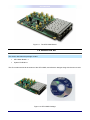
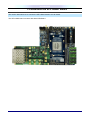
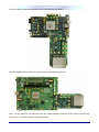
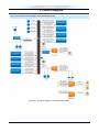
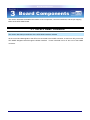
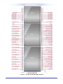
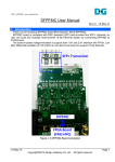
Terasic THDB-SUM SFP HSMC Terasic SFP HSMC Board User Manual Document Version 1.00 AUG 12, 2009 by Terasic Introduction Page Index INTRODUCTION ................................................................................................................................................................................. 1 1.1 1.1 FEATURES..................................................................................................................................................................... 1 1.2 1.2 ABOUT THE KIT ............................................................................................................................................................ 2 1.3 1.3 ASSEMBLE THE SFP HSMC BOARD ........................................................................................................................... 3 1.4 1.4 GETTING HELP ............................................................................................................................................................. 5 ARCHITECTURE ................................................................................................................................................................................ 6 2.1 2.1 LAYOUT AND COMPONETS ............................................................................................................................................ 6 2.2 2.2 BLOCK DIAGRAM .......................................................................................................................................................... 8 BOARD COMPONENTS ................................................................................................................................................................... 9 3.1 3.1 THE SFP HSMC CONNECTOR .................................................................................................................................... 9 3.2 3.2 CLOCK CIRCUITRY...................................................................................................................................................... 15 3.3 3.3 POWER SUPPLY.......................................................................................................................................................... 17 DEMONSTRATION .......................................................................................................................................................................... 18 4.1 4.1 INTRODUCTION ........................................................................................................................................................... 18 4.2 4.2 SYSTEM REQUIREMENTS ........................................................................................................................................... 18 4.3 4.3 SETUP THE DEMONSTRATION .................................................................................................................................... 18 4.4 4.4 DEMO OPERATION ...................................................................................................................................................... 20 4.5 4.5 OVERVIEW .................................................................................................................................................................. 21 APPENDIX ......................................................................................................................................................................................... 23 5.1 5.1 REVISION HISTORY..................................................................................................................................................... 23 5.2 5.2 ALWAYS VISIT SFP HSMC WEBPAGE FOR NEW MAIN BOARD ................................................................................. 23 ii Introduction 1 Introduction The Small Form-Factor Pluggable (SFP) HSMC board is a hardware platform for evaluating the interoperation of Altera FPGA, specifically Stratix IV GX, Arria GX, and Arria II GX, with generic SFP modules. The optical modules that are of particular importance are SGMII Ethernet, Fiber channel, CPRI/OBSAI and SONET. Furthermore, the SFP HSMC board is intended for customers to implement both telecommunication and data communications applications. 1.1 1.1 Features Figure 1.1 shows the photo of the SFP HSMC board. The important features are listed below: 8 SFP Connectors 4 Transceiver Based SFPs 4 LVDS Bases SFPs 8 SMAs 2 Transceiver Receive SMAs 2 Transceiver Transmit SMAs 1 LVDS Clock Input SMA pair (2 SMAs) 2 Single-ended Clock Outputs SMAs 1 LVDS Clock Output SMA pair (2 SMAs) 1 LVPECL Clock Output SMA pair (2 SMAs) Power 12V to 4V 4V to 3.3V Clocks 61.44 MHz 125 MHz 155.52 MHz 156.25 MHz Differential SMA High Speed Mezzanine Card (HSMC) 1 Introduction Figure 1.1. The SFP HSMC Board 1.2 1.2 About the KIT This section describes the package content SFP HSMC Board x 1 System CD-ROM x 1 The CD contains technical documents of the SFP HSMC, and reference designs along with the source code. Figure 1.2 SFP HSMC Package 2 Introduction 1.3 1.3 Assemble the SFP HSMC Board This section describes how to connect the SFP HSMC board to a main board. The SFP HSMC board connects with Altera DE3 Board 3 Introduction The SFP HSMC connects to the Stratix IV GX FPGA Development Board The SFP HSMC board connects with Altera Stratix III FPGA Deveopment Kit Note. Do not attempt to connect/remove the SFP HSMC daughter board to/from the main board when the power is on, or else the hardware could be damaged. 4 Introduction 1.4 1.4 Getting Help Here are some places to get help if you encounter any problem: Email to [email protected] Taiwan & China: +886-3-550-8800 Korea : +82-2-512-7661 Japan: +81-428-77-7000 5 Architecture 2 Architecture This Chapter covers the architecture of the SFP HSMC board including its PCB and block diagram. 2.1 2.1 Layout and Componets The picture of the SFP HSMC board is shown in Figure 2.1 and Figure 2.2. It depicts the layout of the board and indicates the location of the connectors and key components. Figure 2.1. The SFP HSMC PCB and component diagram 6 Architecture Figure 2.2. The SFP HSMC Back side – HSMC connector view The following components are provided on the SFP HSMC board : LVDS SFP[4-7] (J10), XCVR SFP Dip Switch (S5), XCVR LVDS Dip Switch (S4), CLK2_SMA_p (J14), CLK2_SMA_n (J15), SMA_CLK1 (J9), PLL 4:1 Input Multiplexer Dip Switch (S3), PLL 4:1 Input Multiplexer Dip Switch (S2), SMA_REFCLK (J11), SMA_REFCLK_n (J8), SMA_REFCLK_p (J4), CLOCK Dip Switch (S1), XCVR_TX4n (J5), XCVR_TX4p (J1), XCVR_TX4n (J6), XCVR_RX4p (J2), SMA_CLK_n (J7), SMA_CLK_p (J3) HSMC Connector (J17), XCVR SFP[0-3] (J16) 7 Architecture 2.2 2.2 Block Diagram Figure 2.3 shows the block diagram of the SFP HSMC board Figure 2.3. The block diagram of the SFP HSMC board 8 Board Components 3 Board Components This section illustrates the detailed information of the components, connector interfaces, and the pin mapping tables of the SFP HSMC board. 3.1 3.1 The SFP HSMC Connector This section describes pin definition of the SFP HSMC interface onboard All the control and data signals of the SFPs are connected to the HSMC connector, so users can fully control the SFP HSMC daughter board through the HSMC interface. Power is derived from 3.3V and 12V of the HSMC connector. 9 Board Components Figure 3.1. The pin-outs on the HSMC connector 10 Board Components The table 3.1 below lists the HSMC signal direction and description. Pin Name Direction Description 1 N.C. N/A Not Connect 2 N.C. N/A Not Connect 3 N.C. N/A Not Connect 4 N.C. N/A Not Connect 5 N.C. N/A Not Connect 6 N.C. N/A Not Connect 7 N.C. N/A Not Connect 8 N.C. N/A Not Connect 9 N.C. N/A Not Connect 10 N.C. N/A Not Connect 11 N.C. N/A Not Connect 12 N.C. N/A Not Connect 13 XCVR_TX4p Output SMA Transceiver Input 14 XCVR_RX4p Input SMA Transceiver Output 15 XCVR_TX4n Output SMA Transceiver Input 16 XCVR_RX4n Input SMA Transceiver Output 17 SFP3_TDp Output Transmitter Non-Inverted Data Input 18 SFP3_RDp Input Receiver Non-Inverted Data Output 19 SFP3_TDn Output Transmitter Inverted Data Input 20 SFP3_RDn Input Receiver Inverted Data Output 21 SFP2_TDp Output Transmitter Non-Inverted Data Input 22 SFP2_RDp Input Receiver Non-Inverted Data Output 23 SFP2_TDn Output Transmitter Inverted Data Input 24 SFP2_RDn Input Receiver Inverted Data Output 25 SFP1_TDp Output Transmitter Non-Inverted Data Input 26 SFP1_RDp Input Receiver Non-Inverted Data Output 27 SFP1_TDn Output Transmitter Inverted Data Input 28 SFP1_RDn Input Receiver Inverted Data Output 29 SFP0_TDp Output Transmitter Non-Inverted Data Input 30 SFP0_RDp Input Receiver Non-Inverted Data Output 31 SFP0_TDn Output Transmitter Inverted Data Input 32 SFP0_RDn Input Receiver Inverted Data Output 33 N.C. N/A Not Connect 34 N.C. N/A Not Connect 35 N.C. N/A Not Connect Numbers 11 Board Components 36 N.C. N/A Not Connect 37 JTAG_TDO_TDI Inout JTAG data loop through 38 JTAG_TDO_TDI Inout JTAG data loop through 39 N.C. N/A Not Connect 40 N.C. N/A Not Connect 41 SEL[0] Inout CLK 1 Select bit 0 42 SEL[1] Inout CLK 1 Select bit 1 43 SEL[2] Inout CLK 2 Select bit 2 44 SEL[3] Inout CLK 2 Select bit 3 45 3V3 Power Power 3.3V 46 12V Power Power 12V 47 SFP3_TXFAULT Input Module Transmitter Fault 48 SFP3_TXDISABLE Output Transmitter Disable, Turns off transmitter laser output 49 SFP3_MOD2_SDA Input SDA Serial Data Signal 50 SFP3_MOD1_SCL Inout SCL Serial Clock Signal 51 3V3 Power Power 3.3V 52 12V Power Power 12V 53 SFP3_MOD0_PRSNTn Input LED indicator that the module is present 54 SFP3_RATESEL Output Rate Select 55 SFP3_LOS Input Receiver Loss of Signal Indication 56 SFP2_TXFAULT Input Module Transmitter Fault 57 3V3 Power Power 3.3V 58 12V Power Power 12V 59 SFP2_TXDISABLE Output Transmitter Disable, Turns off transmitter laser output 60 SFP2_MOD2_SDA Inout SDA Serial Data Signal 61 SFP2_MOD1_SCL Output SCL Serial Clock Signal 62 SFP2_MOD0_PRSNTn Input LED indicator that the module is present 63 3V3 Power Power 3.3V 64 12V Power Power 12V 65 SFP2_RATESEL Output Rate Select 66 SFP2_LOS Input Receiver Loss of Signal Indication 67 SFP1_TXFAULT Input Module Transmitter Fault 68 SFP1_TXDISABLE Output Transmitter Disable, Turns off transmitter laser output 69 3V3 Power Power 3.3V 70 12V Power Power 12V 71 SFP1_MOD2_SDA Inout SDA Serial Data Signal 72 SFP1_MOD1_SCL Output SCL Serial Clock Signal 73 SFP1_MOD0_PRSNTn Input LED indicator that the module is present 12 Board Components 74 SFP1_RATESEL Output Rate Select 75 3V3 Power Power 3.3V 76 12V Power Power 12V 77 SFP1_LOS Input Receiver Loss of Signal Indication 78 SFP0_TXFAULT Input Module Transmitter Fault 79 SFP0_TXDISABLE Output Transmitter Disable, Turns off transmitter laser output 80 SFP0_MOD2_SDA Inout SDA Serial Data Signal 81 3V3 Power Power 3.3V 82 12V Power Power 12V 83 SFP0_MOD1_SCL Output SCL Serial Clock Signal 84 SFP0_MOD0_PRSNTn Input LED indicator that the module is present 85 SFP0_RATESEL Output Rate Select 86 SFP0_LOS Input Receiver Loss of Signal Indication 87 3V3 Power Power 3.3V 88 12V Power Power 12V 89 SFP4_TDp Output Transmitter Non-Inverted Data Input 90 SFP4_RDp Input Receiver Non-Inverted Data Output 91 SFP4_TDn Output Transmitter Inverted Data Input 92 SFP4_RDn Input Receiver Inverted Data Output 93 3V3 Power Power 3.3V 94 12V Power Power 12V 95 SFP4_TXFAULT Input Module Transmitter Fault 96 CLK1_p Input Differential Clock Input 97 SFP4_TXDISABLE Output Transmitter Disable, Turns off transmitter laser output 98 CLK1_n Input Differential Clock Input 99 3V3 Power Power 3.3V 100 12V Power Power 12V 101 SFP4_MOD2_SDA Inout SDA Serial Data Signal 102 SFP4_MOD1_SCL Output SCL Serial Clock Signal 103 SFP4_MOD0_PRSNTn Input LED indicator that the module is present 104 SFP4_RATESEL Output Rate Select 105 3V3 Power Power 3.3V 106 12V Power Power 12V 107 SFP4_LOS Input Receiver Loss of Signal Indication 108 SFP5_TXFAULT Input Module Transmitter Fault 109 SFP5_TXDISABLE Output Transmitter Disable, Turns off transmitter laser output 110 SFP5_MOD2_SDA Inout SDA Serial Data Signal 111 3V3 Power Power 3.3V 13 Board Components 112 12V Power Power 12V 113 SFP5_TDp Output Transmitter Non-Inverted Data Input 114 SFP5_RDp Input Receiver Non-Inverted Data Output 115 SFP5_TDn Output Transmitter Inverted Data Input 116 SFP5_RDn Input Receiver Inverted Data Output 117 3V3 Power Power 3.3V 118 12V Power Power 12V 119 SFP5_MOD1_SCL Output SCL Serial Clock Signal 120 SFP5_MOD0_PRSNTn Input Not Connect 121 SFP5_RATESEL Output Rate Select 122 SFP5_LOS. Input Receiver Loss of Signal Indication 123 3V3 Power Power 3.3V 124 12V Power Power 12V 125 SFP6_TDp Output Transmitter Non-Inverted Data Input 126 SFP6_RDp Input Receiver Non-Inverted Data Output 127 SFP6_TDn Output Transmitter Inverted Data Input 128 SFP6_RDn Input Receiver Inverted Data Output 129 3V3 Power Power 3.3V 130 12V Power Power 12V 131 SFP6_TXFAULT Input Module Transmitter Fault 132 SFP6_TXDISABLE Output Transmitter Disable, Turns off transmitter laser output 133 SFP6_MOD2_SDA Inout SDA Serial Data Signal 134 SFP6_MOD1_SCL Output SCL Serial Clock Signal 135 3V3 Power Power 3.3V 136 12V Power Power 12V 137 SFP6_MOD0_PRSNTn Input LED indicator that the module is present 138 SFP6_RATESEL Output Rate Select 139 SFP6_LOS Input Receiver Loss of Signal Indication 140 SFP7_TXFAULT Input Module Transmitter Fault 141 3V3 Power Power 3.3V 142 12V Power Power 12V 143 SFP7_TDp Output Transmitter Non-Inverted Data Input 144 SFP7_RDp Input Receiver Non-Inverted Data Output 145 SFP7_TDn Output Transmitter Inverted Data Input 146 SFP7_RDn Input Receiver Inverted Data Output 147 3V3 Power Power 3.3V 148 12V Power Power 12V 149 SFP7_TXDISABLE Output Transmitter Disable, Turns off transmitter laser output 14 Board Components 150 SFP7_MOD2_SDA Inout SDA Serial Data Signal 151 SFP7_MOD1_SCL Output SCL Serial Clock Signal 152 SFP7_MOD0_PRSNTn Input LED indicator that the module is present 153 3V3 Power Power 3.3V 154 12V Power Power 12V 155 SFP7_RATESEL Output Rate Select 156 CLK2_p Input Differential Clock Input 157 SFP7_LOS Input Receiver Loss of Signal Indication 158 CLK2_n Input Differential Clock Input 159 N.C. N/A Not Connect 160 GND Power Power Ground 3.2 3.2 Clock Circuitry This section describes the board’s clock inputs and outputs LVDS clock frequencies of 61.44MHz, 125MHz, 155.52MHz, or 156.25MHz can be selected for HSMC CLK1p/CLK1n. CLK1p/CLk1n will be converted to a single-ended clock signal and output to an SMA. LVDS clock frequencies of 125MHz, 155.52MHz, 156.25MHz, or SMA_CLKp/n can be selected for HSMC CLK2p/CLK2n pins. CLK2p/CLK2n will also be output directly to SMAs. CLK_IN is a single-ended CMOS signal received by the daughter card from the FPGA and is cleaned-up with a frequency synthesizer. The cleaned-up clock is output to an LVPECL SMA pair. 15 Board Components Figure 3.2 Clock Diagram Table 3.2 CLK1 Settings SEL [1:0] CLK1p/CLK1n Frequency 11 125.00 MHz (Default) 10 155.52 MHz 01 156.25 MHz 00 61.44 MHz SEL [3:2] CLK2p/CLK2n Frequency 11 125.00 MHz (Default) 10 155.52 MHz 01 156.25 MHz 00 SMA_CLK_p/n Table 3.3 CLK2 Settings 16 Board Components 3.3 3.3 Power Supply This section describes the power supply on the SFI HSMC board The SFP HSMC is powered through the HSMC connector’s 3.3V and 12V pins. The SFP and clocking circuitry requires 3.3V. A switching regulator powered from the 12 HSMC input produces 4V. Three linear regulators powered from 4V will produce the 3.3V. The switching frequency is set to 1MHz. The power distribution network is shown in the figure below. Max power consumption is estimated at 1A on 12V. Typical power consumption is considerably less than this. Figure 3.3 Power distribution on the SFP HSMC board 17 Demonstration 4 Demonstration This Chapter illustrates the reference designs for the SFP HSMC board 4.1 4.1 Introduction This section describes the functionality of the demonstration briefly. The demonstration shows how to run the SFP HSMC loopback test for both Transceiver/LVDS based channels using the SFP HSMC daughter board and the Stratix IV GX FPGA Development board. The demonstration is intended for users to provide a basic introduction to the SFP HSMC daughter board with the procedure to control different hardware and software settings. 4.2 4.2 System Requirements The following items are required for the HSMC-DVI Server demonstration. SFP HSMC x 1 Stratix IV GX FPGA Development Board x 1 SFP Loopback Connectors x 4 4.3 4.3 Setup the Demonstration Figure 4.3 and 4.4 shows how to setup hardware for the SFP HSMC demonstration. 18 Demonstration Figure 4.3 Transceiver Loopback Test Setup Figure 4.4 LVDS Loopback Test Setup Note: The SFP HSMC board must be connected to HSMC Slot “B” of the Stratix IV GX FPGA Development Board for this demonstration 19 Demonstration 4.4 4.4 Demo Operation This section describes the procedures of running the demonstration FPGA Configuration Demonstration Setup, File Locations, and Instructions Transceiver Loopback Test Demo: Project directory: sfp_hsmb_s4gx_pcie_xcvr_loopback_6p25Gbps_restored Bit Stream used: hsmc_loopback.sof SFP HSMC Setup Insert SFP modules with loopback connectors into SFP ports 0-3 on the SFP HSMC board Set SW5 switches on the SFP HSMC all to the “0” position Stratix IV GX FPGA Development Kit Setup Set SW3 switches 1-3 & 5-8 in the “down” position. Set SW3 switch 4 in the “up” position Set SW4 switches 1,2,4 in the “up” position and switches 3,5,6,8 in the “down” position Set the rotary switch (SW2) to the 0 position Power on the Stratix IV GX FPGA Development Board and download the SOF file (hsmc_loopback.sof) Press and release CPU reset button located on the host board to initiate the test Press and release PB0, enabling comma detect Press and release PB1 enabling channel bonding Press and release PB2, start transmitting PRBS data LED0, LED1, and LED2 should be ON and LED3 should be OFF. Remove one of the SFP modules or one side of a connector so that the loopback will fail. A Failure is indicated on the Stratix IV GX FPGA Dev Kit when LED3 turns ON To reset the board test system, press and release the CPU reset button on the host board Press and release PB1 and PB2 at the same time creates an error in the transmitter data stream, where LED3 should be ON Press and release, the CPU reset button on the host board and verify the results LVDS Loopback Test Demo: Project directory: sfp_hsmb_s4gx_pcie_lvds_loopback_restored Bit Stream used: hsmc_loopback.sof SFP HSMC Setup Insert SFP modules with loopback connectors into SFP ports 4-7 on the SFP HSMC board Set SW4 switches on the SFP HSMC all to the “1” position Stratix IV GX FPGA Development Kit Setup Set SW3 switches 1-4 & 6-8 in the “down” position. Set SW3 switch 5 in the “up” position Set SW4 switches 1,2,4 in the “up” position and switches 3,5,6,8 in the “down” position 20 Demonstration Set the rotary switch (SW2) to the 0 position Power on the Stratix IV GX FPGA Development Board and download the SOF file (hsmc_loopback.sof) Press the CPU reset button located on the host board to initiate the test Press and release PB0, enabling comma detect Press and release PB1 enabling channel bonding Press and release PB2, start transmitting PRBS data LED0, LED1, and LED2 should be ON and LED3 should be OFF. Remove one of the SFP modules or one side of a connector so that the loopback will fail. A Failure is indicated on the Stratix IV GX FPGA Dev Kit when LED3 turns ON To reset the board test system, press and release the CPU reset button on the host board Press and release PB1 and PB2 at the same time creates an error in the transmitter data stream, where LED3 should be ON Press and release, the CPU reset button on the host board and verify the results 4.5 4.5 Overview This section describes the design concepts for the SFP HSMC demonstration. The demonstration is operating on Stratix GX Development Board HSMC Port B interface testing the four Transceiver/LVDS channels at 6.25Gbps. The transceiver signals HSMB[0:3] on the Stratix IV GX FPGA Development board are looped back through the SFP HSMC daughter board. The SFP HSMC board must have SFP modules inserted in SFP[0:3] locations with a loopback from SFP TX to SFP RX on each module. Four transceiver channels of pseudo-random data are 8B/10B encoded, serialized, pre-emphasized and transmitted out according to the following signals HSMB_TX_P/N[3:0] of the Stratix IV GX device at 6.25Gbps. These high-speed serial data are then looped back through an external SFP HSMC back to the Stratix IV GX device. Through the SFP HSMC board the data is then equalized, retimed, deserialized, word aligned, 8B/10B decoded, channel bonded, and then the four bonded channels are compared against a receive side PRBS generator inside the Stratix IV GX FPGA fabric. The demonstration function block diagram is shown below in figure 4.5 21 Demonstration Figure 4.5 SFP Transceiver Test Block Diagram Transceiver/LVDS Loopback Definitions RESET – Resets the Board Test System PB0 – Enable Comma Detect PB1 – Enable Channel Bond PB2 – Start Transmitting PRBS data PB1 & PB2 – Pressing PB1 and PB2 at the same time creates and error in the transmitter data stream USER_LED[0] – PLLs are locked USER_LED[1] – Pattern Sync Acquired (Word aligned, Channel Bonded, 1st PRBS Data Received) USER_LED[2] – Test Complete USER_LED[3] – Error USER_LED[15:4] – Heartbeat Pattern (Board is active) 22 Appendix 5 Appendix 5.1 5.1 Revision History Date Change Log SEPT 1 , 2009 Initial Version April 20 , 2013 Modify some board name 5.2 5.2 Always Visit SFP HSMC Webpage for New Main board We will be continuing providing interesting examples and labs on our SFP HSMC webpage. Please visit www.altera.com or hsmcsfp.terasic.com for more information. 23