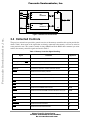
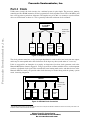
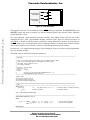
1
Freescale Semiconductor, Inc...
Freescale Semiconductor
AN1769/D
REV. 1.1
1/1999
Application Note
Designing a Minimal PowerPCª System
Gary Milliorn
Motorola RISC Applications
[email protected]
This application note describes how to design a small, high-speed Motorola PowerPCprocessor based system. In this document, the terms Ô60xÕ and Ô7xxÕ are used to denote a
32-bit microprocessor from the PowerPCª architecture family that conforms to the bus
interface of the PowerPC 603eª, PowerPC 604eª, or PowerPC 750ª microprocessors,
respectively. MPC60x and MPC7xx processors implement the PowerPC architecture as it
is speciÞed for 32-bit addressing, which provides 32-bit effective (logical) addresses,
integer data types of 8, 16, and 32 bits, and ßoating-point data types of 32 and 64 bits
(single-precision and double-precision).
This document contains the following topics:
Topic
Page
Part 1, ÒIntroductionÓ
Part 2, ÒProcessor DesignÓ
Part 3, ÒMemory System DesignÓ
Part 4, ÒClockÓ
Part 5, ÒResetÓ
Part 6, ÒPowerÓ
Part 7, ÒInterruptsÓ
For More Information On This Produc
Go to: www.freescale.com
2
3
5
32
33
34
37
Freescale Semiconductor, Inc.
Part 8, ÒCOPÓ
Part 9, ÒPhysical LayoutÓ
Part 10, ÒConclusionÓ
39
42
42
To locate any published errata or updates for this document, refer to the website at
http://www.mot.com/SPS/PowerPC/.
Part 1 Introduction
To keep the design simple, only the most basic features necessary to run a debugger program are included.
These features are as follows:
Freescale Semiconductor, Inc...
¥
¥
¥
¥
¥
¥
A PowerPC processor (this includes the MPC603e, MPC603ev, MPC604, MPE603e, MPE603ev,
MPE604, MPC740 and MPC750)
Flash ROM storage (start-up code)
Read/write memory (downloaded code, program variables)
Serial I/O channel (communication)
Memory and I/O controller
Power, clocks and reset
While this application note is general in focus, it will also occasionally diverge in order to describe the
implementation details of an actual board, known as ÒExcimer,Ó which implements the basic techniques
described in this application note. The details of Excimer provide a base upon which you can build a design,
with the general sections describing ways to support customization.
1.1 Design Philosophy
The PowerPC high-performance family (MPC60x and MPC7xx) bus interface may at Þrst appear
intimidating due to the presence of split address/data bus tenuring, bus snooping, multiprocessing support,
cache coherency support, and other advanced features. Such features can be used to obtain additional
performance for high-performance systems, but for the purposes of a small, high-speed embedded controller
(particularly one with only one bus master), many of these complications can be avoided.
Since the processor does not contain an internal memory controller or I/O interface, that role has
traditionally fallen to the Motorola MPC106 memory/PCI/cache controller. For a small board such as
outlined here, the MPC106 is much more than is minimally needed. Indeed, complexity can sometimes
reduce performance. Cache coherency instructions use valuable bus cycles, and allowing access by external
masters (such as cache) requires delaying memory cycles in case the external device claims the cycle.
Instead, for this design, a programmable ASIC is used to provide the necessary controls for a block of RAM,
ROM and access to I/O. The controller is not programmable by software but is instead pre-conÞgured in
hardware, and memory access cycles are tuned to provide only the necessary signals.
With these restrictions and goals, the typical block diagram may resemble that shown in Figure 1.
Minimal PowerPC System Design
For More Information On This Product,
Go to: www.freescale.com
Freescale Semiconductor, Inc.
Power
Reset
DS1834
LTC1585
Processor
Motorola
MPC60x, MPC7xx,
MPE60x, MPC7xx
Memory Controller
Main Memory
Motorola
(2) MCM69P737
512K PBSRAM
15 ns
Freescale Semiconductor, Inc...
Lattice
2096V
Serial Port
Lattice
16550 UART
Clock
Motorola
MPC904
COP
(optional)
Start-up Code
Motorola
(4) 29F800
TS* 4M Flash
150 ns
I/O Port
Motorola
(2) 74LCX245
Figure 1. Typical Minimal System Block Diagram
1.2 Conventions
Various conventions used in this document are as follows:
SIGNAL
SIGNAL
signal
signal_L
name()
Active-high external signal (pin).
Active-low external signal (pin).
Active-high internal signal (net); used when describing the memory
controller.
Active-low internal signal (net); used when describing the memory
controller (Ô_LÕ indicates active low for internal signals).
A block of HDL code implementing a function.
Occasionally, a name may have both forms; for example, the TS hardware signal may be detected in a
fragment of HDL code which refers to it as Òts_L.Ó
Part 2 Processor Design
The processor may be any member of the MPC60x or MPC7xx family. All such devices offer 64-bit bus
modes, and the MPC603x parts also offer a 32-bit bus interface which can make the memory design even
simpler at a cost of speed. Since only the MPC603x parts support this mode, it will not be used in this design
but it should be kept in mind where the number of parts or cost is even more important than speed.
Since all high-performance PowerPC processors use very similar bus interfaces, the choice of processor
may be based on cost and performance issues and not on the interface costs. For a simple system with only
one bus master, many signals on the processor bus may be ignored or wired to the desired state; refer to
Table 1 for more information.
Minimal PowerPC System Design
For More Information On This Product,
Go to: www.freescale.com
Freescale Semiconductor, Inc.
Table 1. PowerPC Bus Signal Connections1
Freescale Semiconductor, Inc...
Signal
Treatment
AP(0Ð3), APE, BR, CKSTP_OUT, CI, CLKOUT,
CSE(0Ð1), DP(0Ð7), DPE, HALTED, QREQ, RSRV,
TC(0Ð2), TMS, TDI, TDO, VOLTDETGND, WT
Unused, leave unconnected.
CKSTP_IN, DBWO, DBDIS, DRVMOD1, RUN,
SHD, SRESET, TBEN, TLBISYNC, XATS
Unused, pullup or connect to VDD (+3.3V).
L1_TSTCLK, LSSD_MODE
Unused, connect directly to VDD (+3.3V).
ABB, ARTRY, DBB, GBL, L2_TSTCLK,TCK
Unused, connect to 10K pullup to VDD (+3.3V).
BG, DBG, DRVMOD0, L2_INT
Connect to ground.
DRTRY
Connect to HRESET
QACK
Connect to 1K pulldown to ground.
PLL_CFG(0Ð3)
Connect to VDD (+3.3V) or ground to conÞgure CPU speed.
INT, MCP, SMI
Connect to VDD pullup (+3.3V) and/or interrupt controller.
VDD, OVDD
Connect to appropriate voltage level.
AVDD, L2AVDD
Connect to PLL Þlter as shown in hardware reference
manual.
HRESET2
Connect to reset controller.
TRST2
Connect to reset controller, or connect to 1K pulldown (GND).
SYSCLK2
Connect to clock generator.
A(0Ð31), AACK, TA, TEA, TBST, TS, TSIZ(0Ð2),
TT(0Ð4)2
Connect to memory controller.
DH(0Ð31), DL(0Ð31)2
Connect to memory devices.
1
This table combines MPC603x, MPC604x, and MPC750 processors. Not all of these signals are present on
every device.
2
These signals are the only ones that need consideration in a minimal system design. All others are assigned
Þxed values and can be safely ignored thereafter.
The MPC750 has additional signals for interfacing with a back-side L2 cache (L2ADDR[0Ð16],
L2DATA[0Ð63], L2DP[0Ð7], L2CE, L2WE, L2CLK_OUTA, L2CLK_OUTB, L2SYNC_OUT,
L2SYNC_IN, and L2ZZ). Because the L2 interface is completely separate from the system bus, it does not
affect the design of a minimal system in any way. Refer to the MPC750 RISC Microprocessor Hardware
SpeciÞcations, or the MPC750 Processor/Cache Module Hardware Manual, for further details.
Minimal PowerPC System Design
For More Information On This Product,
Go to: www.freescale.com
Freescale Semiconductor, Inc.
Part 3 Memory System Design
Freescale Semiconductor, Inc...
The one fairly complicated portion of a minimal system is the interface to the processor data bus. Unlike
CISC processors, RISC processors do not typically perform data (re)alignment, so the data from each
external device must be placed on the proper data lane. To attempt to use an 8-bit memory device to supply
instructions or data to a 64-bit data bus, 8-bidirectional latching transceivers must be used to move the byte
to the correct byte lane on the 64-bit bus, as shown in Figure 2.
DH(0Ð7)
Latch
DH(8Ð15)
Latch
DH(16Ð23)
Latch
DH(24Ð31)
Latch
DL(0Ð7)
Latch
DL(8Ð15)
Latch
DL(16Ð23)
Latch
DL(24Ð31)
Latch
8-bit
Memory
Device
MPC60x
Memory
Controller
Figure 2. Byte Lane Redirection
Because the processor expects from one to eight bytes on each (non-burst) transfer, the memory controller
must generate from one to eight memory cycles to the 8-bit memory by generating the address(es), latching
the resulting data, and then presenting it to the processor with the TA signal. This process must be reversed
when writing to memory. This can take signiÞcant amounts of logic, and is the approach taken by the
MPC106 ROM interface, for example.
For this minimal system, we will instead take the approach that all memory is 64-bits wide. By using 32-bit
pipelined-burst SRAM for the main memory and 16-bit Flash EPROM for start-up code, only 6 components
will be needed, the controlling logic will be simple and inexpensive, and as a bonus the SRAM will allow
very fast memory access speeds. The use of SRAM for main memory has become more attractive as speed
and size increases and price falls. Currently SRAM devices at 66 MHz are commodity components due to
their use as L2 caches in PCs; even 100-MHz parts are not terribly expensive. The minimal system block
diagram is shown in Figure 3.
Minimal PowerPC System Design
For More Information On This Product,
Go to: www.freescale.com
Freescale Semiconductor, Inc.
I/O Space
MPC60x
A(0:31)
D(0:63)
TT
TSIZ
TBST
TS
AACK
TA
16-bit FlashROM (4X)
TEA
Freescale Semiconductor, Inc...
ADSC
BAA
BWE(0:7)
32-bit Pipelined Burst
SRAM (2X)
CEx
Memory Controller
OEx
Figure 3. Minimal System Memory Architecture
The system address map is shown in Table 2.
Table 2. Excimer Address Map
Address
Devices
Burstable?
Access
Cycles
Start
End
RAM
0x0000_0000
0x3FFF_FFFF
Y
3-1-1-1
Fast I/O
0x4000_0000
0x7FFF_FFFF
N
4
Slow I/O
0x8000_0000
0xBFFF_FFFF
N
12
Flash
0xC000_0000
0xFFFF_FFFF
N
6
The only challenging design problem faced is the handling of burst transfers. The MPC60x family can
operate with caches disabled, thus preventing burst transfers, but this typically exacts a terrible penalty in
performance that makes the additional effort at handling them well worthwhile. The Þrst step in designing
the memory controller (abbreviated MC in code) is to determine the types of controls that will be needed
among the proposed memory devicesÑFlash EPROMs, SRAM and general I/O.
Minimal PowerPC System Design
For More Information On This Product,
Go to: www.freescale.com
Freescale Semiconductor, Inc.
3.1 SRAM Memory Controls
The SRAM interface is centered around the controls necessary for a typical pipelined burst SRAM memory,
as used on the MPC750 back-side cache or various other PC systemÕs L2 cards. Flow-through SRAM
memories could also be used, but the timing for write operations would change. Since this is a simple
memory controller, it will be architected for only one type of SRAM. Most SRAM devices have numerous
controls which are not needed, leaving us with the following:
Freescale Semiconductor, Inc...
A(nÐ0)
Memory address, including LSB for burst transfers and critical-word Þrst.
Addresses 0 and 1 are the LSBs and are used for burst transfer addresses.
Latches address for single-beat or burst transfers
Increments address for burst transfers
Active-low byte-write enables; if not asserted, the cycle is a burst read.
Active-low output enable; asserted for all read operations.
Active-low chip enable; asserted for all operations.
ADSC
ADV
BWE(a-d)
G
SE1
The memory controller must generate these signals for all SRAM transfers, whether single-beat or burst
transfers. ADSC and SE1 start the cycle by latching the address into the SRAM; these must be provided by
the memory controller at the same time. Since SE1 is asserted one clock after TS if the address matches an
SRAM space, the memory controller also asserts ADSC for memory cycles. The BWE signals
corresponding to the size of the transfer must be asserted if the cycle is a write cycle; otherwise, G must be
asserted to read in data (all byte lanes are driven and the processor selects the data from whichever byte lane
is needed).
The remaining signal is ADV, which must be asserted for three clock cycles if a burst transfer is selected;
otherwise, it remains high. Although the data rate could be throttled with ADV or G, this is not necessary
for the processor, so, to simplify the design, only fast SRAMs will be accommodated.
The remaining portion of the SRAM controller to specify is the initial access time. Most SRAMs available
today can decode an address within 10 ns from the address strobe (ADSC), so there is no need to delay
before beginning a transfer.
VDD
ADSP
SGW
SE2
ADSC
ADV
MPC750
SB(AÐD)
MCM69P737
LBO
SE3
SW
G
TS
SE1
GND
VDD
ADSC
BAA
Memory BWE(0Ð7)
Controller
ADSP
SGW
SE2
ADSC
ADV
SB(AÐD)
SOE
G
SCS
SE1
MCM69P737
LBO
SE3
SW
GND
Figure 4. Pipelined Burst SRAM Memory Connections
Minimal PowerPC System Design
For More Information On This Product,
Go to: www.freescale.com
Freescale Semiconductor, Inc.
Note that since we do not allow overlapped address and data tenures, we do not know whether the next
transfer is to the same SRAM page or not, so we cannot stream data (that is, 3-1-1-1/1-1-1-1/... cycles). This
requires much more logic and is left as an exercise for the reader.
A Þnal issue which must be handled is terminating an access. Burst SRAMÕs operate by streaming data into
or out of the chip on each clock edge after an initial setup sequence (ADSC), until instructed to stop. While
read operations can be ignored by forcing G high, write operations cannot be similarly controlled, so instead
a Òde-selectÓ cycle must be performed after each access. This is done by asserting ADSC without no chip
select asserted; when deselected, the SRAM will stop reading or writing data.
Freescale Semiconductor, Inc...
3.2 Flash Memory Controls
Flash memory devices use traditional OE, CS and WE signals to perform single-beat read and write cycles
(burst transfers are not permitted1), whether the data width of the device is 8-bits or 16-bits. Since the
PowerPC bus does not care if data is placed on ignored byte lanes during read cycles, it will be acceptable
to use OE in common for all ßash ROMs.
Write cycles require more care. Requiring the processor to perform 64-bit writes is unacceptable because it
is difÞcult (that is, requires the ßoating-point unit on the MPC devices) or impossible (on the non-ßoatingpoint MPE devices) to do a 64-bit single-beat bus transfer. Thus, ßash devices must be fully-qualiÞed with
byte-enables during write cycles.
Using standard ßash devices will require the following control signals:
BWE(0Ð7)
FOE
Active-low byte-write enables; if not asserted, the cycle is a read.
Active-low output enable; asserted for all read operations.
FCS
Active-low chip enable; asserted for all operations.
This gives a ßash memory architecture as shown in Figure 5.
BWE0
WE
FOE
OE
FCS
CS
BWE2
WE
OE
M29F800
(16-bit)
BYTE
3.3V
M29F800
(16-bit)
BYTE
3.3V
Remember:
3.3V Devices
ONLY!
CS
BWE4
WE
OE
M29F800
(16-bit)
BYTE
3.3V
M29F800
(16-bit)
BYTE
3.3V
CS
BWE6
WE
OE
CS
Figure 5. Flash Memory Connections
1
This implies that the ROM space is non-cacheable; since Flash ROM is so much slower than SRAM, critical code should be copied to SRAM, so this
may not be considered a big performance limitation.
Minimal PowerPC System Design
For More Information On This Product,
Go to: www.freescale.com
Freescale Semiconductor, Inc.
Note that 16-bit devices have been used. This helps reduce the number of components, at a cost of restricting
writes to 16, 32 or 64 bits in size. If 8-bit writes are required, then either 8 8-bit devices must be used, or
devices which have multiple byte enables.
A further restriction on ßash memory is that reading is slow (from 60 to 200 ns), and writing is even slower
(as much as 15 ms). The memory controller delays the assertion of TA for a Þxed number of cycles on any
access to match the read time; this handles the read access properly and gives sufÞcient time for the ßash
device to begin the program operation (the data does not need to be held throughout a write cycle).
Software must insure that a proper amount of time has elapsed after a write before another read or write
occurs. This can be done with a simple timing loop, using I/O to check the RDY/BSY signals, or the use of
ßash devices which can be queried by reading special addresses.
Freescale Semiconductor, Inc...
3.3 I/O Controls
Most simple I/O devices such as real-time clocks, serial ports, and other unique interfaces have fairly simple
I/O controlsÑa chip select, an output enable, and a write control. The I/O controller can then be modeled
very closely on the ßash ROM controller; both have simple controls and both are relatively slow.
One difference between ßash ROM and I/O is that most I/O devices are 8 or perhaps 16 bits, not 64, so I/O
devices must be attached to particular byte lanes. The I/O controller responds to any size write, so data may
be placed on any byte lane (software is responsible for positioning and retrieving the data properly). A fairly
easy modiÞcation to the controller allows different I/O times for each address decoded, allowing fast and
slow I/O devices to be mixed.
Note that the write strobes/direction control are the same byte write enables that have been described before.
This reuse will allow a reduction of the size and complexity of the controller, but it also means that the
software must generate the correct address when performing writes to I/O devices greater than 8 bits wide.
For example, in Figure 6, a 16-bit I/O device is attached to D(0Ð15) and uses BWE1, so to access the
controller, software must issue 16- or 32-bit writes aligned with D0. The controller will assert BWE1 (all
others are ignored).
XOE
RD
BWE0
WE
XCS0
CS
PC
I/O Device
D(0Ð7)
Remember:
3.3V Devices
ONLY!
OE
BWE1
R/W
XCS1
CS
Motorola
I/O Device
D(0Ð15)
Figure 6. I/O Connections
The I/O controller supports both Motorola and PC control signals. In addition, these devices attach to the
3.3-V PowerPC data bus, so they must not drive over 3.3V. An easy solution to this is to add a 3.3-V buffer
between the high-speed memory path and the I/O devices, which has a side beneÞt of allowing faster
memory operation due to reduced capacitive loading.
Minimal PowerPC System Design
For More Information On This Product,
Go to: www.freescale.com
Freescale Semiconductor, Inc.
XOE
OE
RD
BWE0
WE
XCS0
CS
5V
I/O Device
LVT245
D(0Ð7)
OE
R/W
XCS1
3.3V
I/O Device
CS
DIR
Freescale Semiconductor, Inc...
Figure 7. Buffered I/O Connections
3.4 Collected Controls
The previous sections have provided a general overview of the memory controller; this section provides the
details. Table 1 shows most of the signals that are directly connected to the memory or I/O or are wired to
some particular state. The controls needed for burst SRAM and ßash ROM share common byte-write
enables; the memory controller signals are listed in Table 3.
Table 3. Memory Controller Signal Handling
Signal
Treatment
Applies To
TS
Examined for start of a cycle
All
TT(0Ð4), TSIZ(0Ð2), TBST
Examined for type of cycle
All
A(0Ð1)
Examined for cycle destination (RAM, ROM, I/O)
All
A(29Ð31)
Examined for byte lane enables and burst transfer
All
AACK
Asserted on Þnal memory transfer
All
TA
Asserted per-beat on each memory transfer
All
TEA
Asserted on each unsupported memory transfer
All
BWE(0Ð7)
Asserted on writes on individual byte lane(s)
SRAM, ROM
SCS
Asserted on all SRAM accesses
SRAM
SOE
Asserted on all SRAM read accesses
SRAM
ADSC
Asserted on all burst SRAM accesses before the Þrst cycle
SRAM
BAA
Asserted on all burst SRAM accesses during cycles 2-4
SRAM
FCS
Asserted on all Flash accesses
ROM
FOE
Asserted on all Flash read accesses
ROM
XCS(0Ð1)
Asserted on all I/O accesses
I/O
XOE
Asserted on all I/O read accesses
I/O
Minimal PowerPC System Design
For More Information On This Product,
Go to: www.freescale.com
Freescale Semiconductor, Inc.
All other signals are either wired to the necessary state or are unused as described in Table 1. For example,
since the PowerPC bus is parked permanently, detecting BG, ABB, DBG and DBB are unnecessary. The
memory controller interface then requires a total of 35 I/O signals, well within the capacity of any modern
FPGA, leaving lots of I/O for additional functions.
3.5 Memory Controller Details
The remainder of Part 3, ÒMemory System Design,Ó describes the internal operations of the memory
controller as used on the Excimer reference board. The code is based upon synthesizable VHDL code, but
could be easily adapted to Verilog, and any of the several IC-speciÞc HDL variants that exist for Actel,
Altera, Lattice, Xilinx et. al.
Freescale Semiconductor, Inc...
Figure 8 shows the internal architecture of the memory controller module.
SCS
SOE
FCS
chipsel()
A(0Ð1)
FOE
XCS(0Ð1)
TT(0Ð4)
XOE
CTIME(0Ð3)
TS
start()
CLAIM_L
DOERR_L
ADSC
WE_L
A(29Ð31)
BWE(0Ð7)
bytedec()
TSIZ(0Ð2)
TBST
AACK
cycler()
BAA
TA
RST
TEA
CLK
Figure 8. Memory Controller Architecture
3.5.1 Start Detection Module
Upon receiving a TS, the memory controller must examine the TT(0Ð4) signals to determine the type of
cycle that will be performed. Of the 32 possible permutations, only those found in Table 4 are of interest:
Minimal PowerPC System Design
For More Information On This Product,
Go to: www.freescale.com
Freescale Semiconductor, Inc.
Table 4. TT Encoding
TT0
TT1
TT2
TT3
TT4
Transaction
Memory Controller Action
0
0
0
1
0
Write-with-ßush
Single-beat or burst write
0
0
1
1
0
Write-with-kill
Burst write
0
1
0
1
0
Read
Single-beat or burst read
0
1
1
1
0
Read-with-intent-to-modify
Burst read
Freescale Semiconductor, Inc...
All remaining TT codes are either address-only cycles (which are not needed), are caused by instructions
not needed in single-processor environments (for example, the eciwx, ecowx, dcbz, lwarx, and stcwx
instructions), or are reserved values. These simpliÞcations are possible because there is no need to snoop
the processor bus to maintain cache coherency.
While software should not generate such cycles, it is not reliable for a memory controller to simply ignore
them. The memory controller, as the sole target of bus transactions, must terminate unacceptable bus cycles
with TEA; otherwise, the processor will wait forever for the (ignored) cycle to complete.
When any transfer begins, the Òstart()Ó module must either assert the Òclaim_lÓ or Òdoerr_lÓ signal to cause
the appropriate actions to conclude the transfer cycle (which is handled in the bus state machine Òcycler()Ó).
The general architecture of Òstart()Ó is shown in Figure 9.
5
TT(0Ð4)
ttdec()
WE_L
TS
AACK
start()
CLK
CLAIM_L
DOERR_L
RST
Figure 9. Start Detector Module
The TT(0Ð4) signals do not change during the address tenure, whether burst or single-beat, so the outputs
remain valid until the memory controller asserts AACK. The Òstart()Ó module provides the global
CLAIM_L signal, used by other modules to detect whether a cycle is in-progress, or the DOERR_L signal,
used to terminate unclaimed cycles, and a write signal (WE_L) to determine that the cycle is a write cycle.
These signals are used exclusively by other modules, and remain valid until the memory controller
completes the cycle by asserting AACK.
The VHDL code for this module is:
------------------------------------------------------------------------------------------------- TTDEC.VHD
--- TTDEC() monitors the TT bus and determines whether the TT is of interest to
-- the MC or not. If so, a signal is provided for start, and tt_we_L reflects
-- the read/write status.
--- NOTE: TTDEC must not be optimized or errors will occur when hierarchical
-optimization is performed (TT1 and TT2 will be optimized away, making it
-impossible to connect TTDEC to MC-- this is a bug in ViewSynthesis).
-Recommended procedure is to dissolve TTDEC into it's parent level MC
Minimal PowerPC System Design
For More Information On This Product,
Go to: www.freescale.com
Freescale Semiconductor, Inc.
-before optimization. ViewSynthesis doesn't seem to care about the NC
-input pins at that level.
--- Copyright 1998, by Motorola Inc.
-- All rights reserved.
--- Author: Gary Milliorn
-- Revision: 0.1
-- Date:
6/10/98
-- Notes:
-All logic is active low when appended with a "_L".
-Passed speedwave check 6/16/98.
-------------------------------------------------------------------------------------------------
Freescale Semiconductor, Inc...
library ieee;
use ieee.std_logic_1164.all;
use ieee.std_logic_arith.all;
use ieee.std_logic_unsigned.all;
------------------------------------------------------------------------------------------------- TTDEC
-----------------------------------------------------------------------------------------------ENTITY TTDEC is
PORT( tt
: in
std_logic_vector( 0 to 4 ); -- current transfer type.
tt_take
: buffer std_logic;
-- asserted when TT matches types.
tt_we_L
: buffer std_logic;
-- asserted when cycle is write.
monitor
: buffer std_logic
-- ViewSynthesis bug -- not useful.
);
end; --PORT DEFINITION AND ENTITY
-----------------------------------------------------------------------------------------------ARCHITECTURE BEHAVIOR OF TTDEC is
SIGNAL wflush, wkill, read, rwim
: std_logic;
BEGIN
-- Detect only the following TT types. "tt_take" will be asserted for all cycles we will claim.
-wflush <= '1' WHEN (tt(0) = '0' and tt(1) = '0' and tt(2) = '0' and tt(3) = '1' and tt(4) = '0')
ELSE '0';
wkill
<= '1' WHEN (tt(0) = '0' and tt(1) = '0' and tt(2) = '1' and tt(3) = '1' and tt(4) = '0')
ELSE '0';
read
<= '1' WHEN (tt(0) = '0' and tt(1) = '1' and tt(2) = '0' and tt(3) = '1' and tt(4) = '0')
ELSE '0';
rwim
<= '1' WHEN (tt(0) = '0' and tt(1) = '1' and tt(2) = '1' and tt(3) = '1' and tt(4) = '0')
ELSE '0';
tt_take <= (wflush or wkill or read or rwim);
tt_we_L <= not (wflush or wkill);
-- Needed due to ViewSynthesis bug: optimizes tt1 and tt2 away, then complains about their absence.
monitor <= read;
END BEHAVIOR;
------------------------------------------------------------------------------------------------- START.VHD
--- START() is the portion of the memory controller which decodes incoming
-- transfers and decides whether they should be claimed by the controller
-- or terminated with an error condition.
--- Copyright 1998, by Motorola Inc.
-- All rights reserved.
--- Author: Gary Milliorn
-- Revision: 0.3
-- Date:
9/23/98
-- Notes:
-All logic is active low when appended with a "_L".
-Passed speedwave check 6/16/98.
-Moved ADSC* assertion to state machine.
------------------------------------------------------------------------------------------------library ieee;
use ieee.std_logic_1164.all;
Minimal PowerPC System Design
For More Information On This Product,
Go to: www.freescale.com
Freescale Semiconductor, Inc.
use ieee.std_logic_arith.all;
use ieee.std_logic_unsigned.all;
--==============================================================================================
-- START
-----------------------------------------------------------------------------------------------ENTITY START is
PORT( tt_take
: in
std_logic;
-- asserted if good TT selection.
tt_we_L
: in
std_logic;
-- asserted if good TT is write.
ts_L
: in
std_logic;
-- transfer start strobe.
aack_L
: in
std_logic;
-- asserted on transfer complete.
clk
: in
std_logic;
-- bus clock.
rst_L
: in
std_logic;
-- system reset.
claim_L
: buffer std_logic;
-- asserted when cycle is claimed.
doerr_L
: buffer std_logic;
-- asserted when cycle not claimed.
we_L
: buffer std_logic
-- byte lane write selects.
);
Freescale Semiconductor, Inc...
end; --PORT DEFINITION AND ENTITY
-----------------------------------------------------------------------------------------------ARCHITECTURE BEHAVIOR OF START is
BEGIN
-- Derive a D flop to maintain selected status. The register must be globally clocked to fit
-- well in the Lattice 2xxx FPGA architecture, where clocks and resets are global (or expensive).
monitor : PROCESS( clk, rst_L )
BEGIN
IF (rst_L = '0') THEN
we_L
<= '1';
claim_L <= '1';
doerr_L <= '1';
ELSIF (clk'EVENT and clk = '1') THEN
IF (
(ts_L = '0'
and tt_take = '1')
or (claim_L = '0' and aack_L = '1')) THEN
claim_L <= '0';
we_L
<= tt_we_L;
ELSE
claim_L <= '1';
we_L
<= '1';
END IF;
IF ( (ts_L = '0'
and tt_take = '0')
or (doerr_L = '0' and aack_L = '1')) THEN
doerr_L <= '0';
ELSE
doerr_L <= '1';
END IF;
END IF;
END PROCESS;
-- TS and something we want.
-- claimed, but not AACK'd
-- else AACK or no-claim
-- TS and something we dont' want.
-- errored, but not AACK'd
-- else AACK or claim
END BEHAVIOR;
------------------------------------------------------------------------------------------------
3.5.2 Byte Write Enable
The next group of signals to generate are the byte lane write enables BWE(0Ð7). These signals are generated
by using the transfer size signals TSIZ(0Ð2) along with the lower address bus signals A(29Ð31) to determine
which byte lanes should be active.
Minimal PowerPC System Design
For More Information On This Product,
Go to: www.freescale.com
Freescale Semiconductor, Inc.
3
A(29Ð31)
3
TSIZ(0Ð2)
bytedec()
8
BWE(0Ð7)
TBST
we_L
Freescale Semiconductor, Inc...
Figure 10. Byte Write Enable Module
Note that the Òbytedec()Ó module examines the decoded write status (WE_L) but not CLAIM, so the byte
lane enables are asserted for all write cycles regardless of the activity of the CLAIM signal. This is
acceptable as long as the corresponding chip-select signals disable the attached memory and I/O devices,
which is true for the devices used.
The VHDL code for the Òbytedec()Ó module is lengthy but straightforward. The values are directly derived
from the data alignment tables in the processor user manuals, for example Table 8-3 and Table 8-4 of the
MPC750 RISC Microprocessor UserÕs Manual. Burst transfers enable all byte lanes, while all other
transfers enable only the byte lanes based upon the address and transfer size.
------------------------------------------------------------------------------------------------- BYTEDEC.VHD
--- BYTEDEC() is the portion of the MC which provides
-- individual byte write enabled for each byte lane, depending upon
-- the size and address of the transfer. If the cycle is a read cycle,
-- no outputs are asserted at all.
--- Copyright 1998, by Motorola Inc.
-- All rights reserved.
--- Author: Gary Milliorn
-- Revision: 0.1
-- Date:
6/10/98
-- Notes:
-All logic is active low when appended with a "_L".
-Passed speedwave check 6/10/98.
------------------------------------------------------------------------------------------------library ieee;
use ieee.std_logic_1164.all;
use ieee.std_logic_arith.all;
use ieee.std_logic_unsigned.all;
-----------------------------------------------------------------------------------------------ENTITY BYTEDEC is
PORT(
a
: in
std_logic_vector( 29 to 31 ); -- stable 60X bus address
tsiz
: in
std_logic_vector( 0 to 2 ); -- current transfer size.
tbst_L
: in
std_logic;
-- asserted if transfer is burst.
we_L
: in
std_logic;
-- asserted if transfer is write.
bwe_L
: buffer std_logic_vector( 0 to 7 )
-- byte lane write selects.
);
end; --PORT DEFINITION AND ENTITY
-----------------------------------------------------------------------------------------------ARCHITECTURE BEHAVIOR OF BYTEDEC is
SIGNAL be_L : std_logic_vector( 0 to 7 );
-- byte lane enables (read or write).
BEGIN
-- Convert transfer size and address into byte lane enables. Write masking
-- occurs later.
be_L(0) <= '0'
WHEN (
or
or
or
or
(tsiz
(tsiz
(tsiz
(tsiz
(tsiz
=
=
=
=
=
"001"
"010"
"100"
"000"
"011"
and
and
and
and
and
a
a
a
a
a
=
=
=
=
=
"000")
"000")
"000")
"000")
"000")
------
byte
half-word
word
double-word
three-byte
Minimal PowerPC System Design
For More Information On This Product,
Go to: www.freescale.com
Freescale Semiconductor, Inc.
Freescale Semiconductor, Inc...
or (tbst_L = '0')
)
ELSE '1';
-- burst
be_L(1) <= '0'
WHEN ( (tsiz =
or (tsiz =
or (tsiz =
or (tsiz =
or (tsiz =
or (tsiz =
or (tbst_L
)
ELSE '1';
"001"
"010"
"100"
"000"
"011"
"011"
= '0')
and
and
and
and
and
and
a
a
a
a
a
a
=
=
=
=
=
=
"001")
"000")
"000")
"000")
"000")
"001")
--------
byte
half-word
word
double-word
three-byte
three-byte
burst
be_L(2) <= '0'
WHEN ( (tsiz =
or (tsiz =
or (tsiz =
or (tsiz =
or (tsiz =
or (tsiz =
or (tsiz =
or (tbst_L
)
ELSE '1';
"001"
"010"
"100"
"000"
"011"
"011"
"011"
= '0')
and
and
and
and
and
and
and
a
a
a
a
a
a
a
=
=
=
=
=
=
=
"010")
"010")
"000")
"000")
"000")
"001")
"010")
---------
byte
half-word
word
double-word
three-byte
three-byte
three-byte
burst
be_L(3) <= '0'
WHEN ( (tsiz =
or (tsiz =
or (tsiz =
or (tsiz =
or (tsiz =
or (tsiz =
or (tsiz =
or (tbst_L
)
ELSE '1';
"001"
"010"
"100"
"000"
"011"
"011"
"011"
= '0')
and
and
and
and
and
and
and
a
a
a
a
a
a
a
=
=
=
=
=
=
=
"011")
"010")
"000")
"000")
"001")
"010")
"011")
---------
byte
half-word
word
double-word
three-byte
three-byte
three-byte
burst
be_L(4) <= '0'
WHEN ( (tsiz =
or (tsiz =
or (tsiz =
or (tsiz =
or (tsiz =
or (tsiz =
or (tsiz =
or (tbst_L
)
ELSE '1';
"001"
"010"
"100"
"000"
"011"
"011"
"011"
= '0')
and
and
and
and
and
and
and
a
a
a
a
a
a
a
=
=
=
=
=
=
=
"100")
"100")
"100")
"000")
"010")
"011")
"100")
---------
byte
half-word
word
double-word
three-byte
three-byte
three-byte
burst
be_L(5) <= '0'
WHEN ( (tsiz =
or (tsiz =
or (tsiz =
or (tsiz =
or (tsiz =
or (tsiz =
or (tsiz =
or (tbst_L
)
ELSE '1';
"001"
"010"
"100"
"000"
"011"
"011"
"011"
= '0')
and
and
and
and
and
and
and
a
a
a
a
a
a
a
=
=
=
=
=
=
=
"101")
"100")
"100")
"000")
"011")
"100")
"101")
---------
byte
half-word
word
double-word
three-byte
three-byte
three-byte
burst
be_L(6) <= '0'
WHEN ( (tsiz =
or (tsiz =
or (tsiz =
or (tsiz =
or (tsiz =
or (tsiz =
or (tbst_L
)
ELSE '1';
"001"
"010"
"100"
"000"
"011"
"011"
= '0')
and
and
and
and
and
and
a
a
a
a
a
a
=
=
=
=
=
=
"110")
"110")
"100")
"000")
"100")
"101")
--------
byte
half-word
word
double-word
three-byte
three-byte
burst
be_L(7) <= '0'
WHEN ( (tsiz =
or (tsiz =
or (tsiz =
or (tsiz =
or (tsiz =
or (tbst_L
)
ELSE '1';
"001"
"010"
"100"
"000"
"011"
= '0')
and
and
and
and
and
a
a
a
a
a
=
=
=
=
=
"111")
"110")
"100")
"000")
"101")
-------
byte
half-word
word
double-word
three-byte
burst
-- Now mask the byte lanes with the write signal.
bwe_L(0) <= (be_L(0) or we_L);
bwe_L(1) <= (be_L(1) or we_L);
bwe_L(2) <= (be_L(2) or we_L);
Minimal PowerPC System Design
For More Information On This Product,
Go to: www.freescale.com
Freescale Semiconductor, Inc.
bwe_L(3)
bwe_L(4)
bwe_L(5)
bwe_L(6)
bwe_L(7)
<=
<=
<=
<=
<=
(be_L(3)
(be_L(4)
(be_L(5)
(be_L(6)
(be_L(7)
or
or
or
or
or
we_L);
we_L);
we_L);
we_L);
we_L);
END BEHAVIOR;
------------------------------------------------------------------------------------------------
The three-byte cycles arise from the need to handle misaligned transfers by breaking them into two separate
cycles; refer to the MPC603e and EC603e RISC Microprocessor UserÕs Manual or the MPC750 RISC
Microprocessor UserÕs Manual for details on this process. These cycles do not occur if unaligned transfers
do not occur. Since many C compilers do not generate such code, the lines for three-byte handling can be
deleted to simplify the controller and reduce gate count.
Freescale Semiconductor, Inc...
3.5.3 Chip Select
The chip-select module, shown in Figure 11, generates the four chip-select signals and selects the proper
time delay for accesses to memory (this information is used by the Òcycler()Ó module).
2
SCS
SOE
A(0Ð1)
FCS
FOE
chipsel()
WE_L
XCS(0Ð1)
XOE
4
CLAIM_L
CTIME(0Ð3)
Figure 11. Chip Select Module
Table 5 shows the chip-select actions based upon the address.
Table 5. Chip Select Encodings
A(0Ð1)
I/O Area
Time (66 MHz)
Bus Clock Count
Timer Value
00
High-speed SRAM array
N/A
N/A
N/A
01
High-speed I/O
60 ns
4
1
10
Slow-speed I/O
180 ns
12
9
11
Flash boot ROM
80 ns
6
3
The timer values in Table 5 have a constant overhead of three subtracted from the expected timer values.
This constant overhead is due to the start delay, the Þnal TA assertion, and one clock needed to detect a zerocount on the timer. So for best performance, the actual timer values are offset by (-3). In examining chipsel(),
the SRAM chip select is found to be fairly straightforward; the other chip selects differ in that a 4-bit timer
value is generated to add delay to the assertion of TA.
Minimal PowerPC System Design
For More Information On This Product,
Go to: www.freescale.com
Freescale Semiconductor, Inc.
The code for this module is:
Freescale Semiconductor, Inc...
------------------------------------------------------------------------------------------------- CHIPSEL.VHD
--- CHIPSEL() is the portion of the MC which decodes addresses
-- and provides corresponding chip select outputs, along with a clock
-- timer value which determines the rate of memory accesses.
--- Copyright 1998, by Motorola Inc.
-- All rights reserved.
--- Author: Gary Milliorn
-- Revision: 0.2
-- Date:
6/10/98
-- Notes:
-All logic is active low when appended with a "_L".
-Passed speedwave check 6/16/98.
-----------------------------------------------------------------------------------------------library ieee;
use ieee.std_logic_1164.all;
use ieee.std_logic_arith.all;
use ieee.std_logic_unsigned.all;
------------------------------------------------------------------------------------------------- CHIPSEL
-----------------------------------------------------------------------------------------------ENTITY CHIPSEL is
PORT( a
: in
std_logic_vector( 0 to 1 ); -- stable 60X bus address
claim_L
: in
std_logic;
-- asserted for active cycles.
we_L
: in
std_logic;
-- asserted for write cycles.
scs_L, soe_L
: buffer std_logic;
-- SRAM chip-selects & enables.
fcs_L, foe_L
: buffer std_logic;
-- Flash chip-selects & enables.
xcs_L
: buffer std_logic_vector( 0 to 1 ); -- I/O chip selects.
xoe_L
: buffer std_logic;
-- I/O output enable.
ctime
: buffer std_logic_vector( 3 downto 0 )-- 4-bit time value.
);
end; --PORT DEFINITION AND ENTITY
-----------------------------------------------------------------------------------------------ARCHITECTURE BEHAVIOR OF CHIPSEL is
BEGIN
-- Assert chip select if cycle is claimed and
scs_L <= Õ0Õ
WHEN (a = "00" and claim_L
ELSE Õ1Õ;
xcs_L(0) <= Õ0Õ WHEN (a = "01" and claim_L
ELSE Õ1Õ;
xcs_L(1) <= Õ0Õ WHEN (a = "10" and claim_L
ELSE Õ1Õ;
fcs_L <= Õ0Õ
WHEN (a = "11" and claim_L
ELSE Õ1Õ;
corresponding address is presented.
= Õ0Õ)
= Õ0Õ)
= Õ0Õ)
= Õ0Õ)
-- Assert corresponding output enables (OE_L) if
-- a write cycle.
soe_L <= Õ0Õ
WHEN ( a = "00" and claim_L
ELSE Õ1Õ;
xoe_L <= Õ0Õ
WHEN ( (a = "01" and claim_L
or (a = "10" and claim_L
ELSE Õ1Õ;
foe_L <= Õ0Õ
WHEN ( a = "11" and claim_L
ELSE Õ1Õ;
-----
the cycle is claimed and is not
= Õ0Õ and we_L = Õ1Õ)
= Õ0Õ and we_L = Õ1Õ)
= Õ0Õ and we_L = Õ1Õ))
= Õ0Õ and we_L = Õ1Õ)
Provide corresponding timer value. Note that SRAM is not timer controlled, so any
value may be used. All of these values should be changed if the bus frequency is
changed. If the clock rate is increased, the system may fail. If lowered, clock
cycles will be wasted.
-- Note: there is a three clock overhead in the setup and termination of timed cycles
-- (one on entry, one during AACK/TA*, and one exiting when the timer is zero). Therefore,
-- timing constants are offset by (-3).
SET_TIMER : PROCESS( fcs_L, xcs_L(0) )
BEGIN
IF (fcs_L = Õ0Õ) THEN
ctime <= "0011";
-- Flash:
80 ns @ 15ns clocks (66 MHz) = 6 -3 => 3 clocks.
Minimal PowerPC System Design
For More Information On This Product,
Go to: www.freescale.com
Freescale Semiconductor, Inc.
ELSIF (xcs_L(0) = Õ0Õ) THEN
ctime <= "1001";
ELSE
ctime <= "0001";
END IF;
END PROCESS SET_TIMER;
-- Slow I/O: 180 ns @ 15ns clocks (66 MHz) = 12 -3 => 9 clocks.
-- Fast I/O: 60 ns @ 15ns clocks (66 MHz) = 4 -3 => 1 clocks.
END BEHAVIOR;
------------------------------------------------------------------------------------------------
The chipsel() module is asynchronous because it relies on the synchronous signal, claim_L, and relies on
the stability of the address bus (a) and write select (we_L) signals. These latter two signals are guaranteed
to be stable until TA is asserted because the cycler() module also delays the assertion of AACK until the last
TA.
Freescale Semiconductor, Inc...
The chip-select module may be easily adapted to different device speeds, and for different I/O maps (within
PowerPC architecture limitations). It may also be modiÞed to provide access to internal register Þles or to
increase the number of chip selects, within limitations of the FPGA chosen.
3.5.4 Cycler State Machine
The cycler() state machine module controls the remainder of any transaction claimed by the memory
controller. For optimal performance, one of four ßows are selected. The ßows are as follows:
¥
¥
¥
¥
SRAM single beat transfer
SRAM burst transfer
Programmed-length transfer (I/O and Flash)
Error transactions
The Þrst two optimize speed for the SRAM accesses, which are typically the majority of code and data
accesses; the latter are handled in a more programmed method. Fortunately, the streamlined nature of burst
transfers keeps the cycler() module from becoming too complicated.
Cycler() Þnishes any non-error transaction by asserting AACK and TA (one to four times, based upon the
type of cycle). When AACK is generated, the cycle has been completed and a new one can begin at the next
clock cycle. Due to the pipelining nature of the SRAM, it actually takes 5 beats to do a read cycle, but one
of those clock cycles has already been provided before cycler() can leave the IDLE state by the synchronous
start() detector. Figure 12 shows the end-cycle module.
CTIME(0Ð3)
4
TEA
CLAIM_L
AACK
DOERR_L
cycler
SCS_L
BAA
TBST
TA
RST
ADSC
CLK
Figure 12. End-Cycle Module
As the VHDL code for the cycler() is generated by a state-machine CAD program, the code is uncommented
and somewhat difÞcult to follow; refer instead to Figure 13 for details.
Minimal PowerPC System Design
For More Information On This Product,
Go to: www.freescale.com
Freescale Semiconductor, Inc.
CYCLER.DIA
Cycler - Milliorn 98SEP25
!RST_L
DESEL
!CLAIM_L &
!SCS_L &
!TBST_I
IDLE
!DOERR_L
!CLAIM_L &
SCS_L &
TBST_
!CLAIM_L &
!SCS_L &
TBST_
BURST
COUNT
TIMER = CTIME;
ERROR
Freescale Semiconductor, Inc...
BEAT1
SINGLE
TIMER <> "0000"
COUNT
TIMER £ TIMER Ð 1;
WE_L
!WE_L
BEAT2
TIMER = "0000"
BEAT3
Moore Machine State Outputs
AACK_L = not (BEAT4 or ERROR)
ADSC_L = not ( (IDLE and !SCS_L and !CLAIM_L)
or DESEL)
BAA_L = not ( (BURST or BEAT1 or BEAT2)
or (BEAT4 and !WE_L and !TBST_L)
TA_L =
BEAT4
not ( (BEAT1 or BEAT2 or BEAT3 or BEAT4)
or (!TBST_L and !WE_L)
or (BURST and !WE_L) )
TEA_L = not ( ERROR )
Vector Declarations
CTIME[] = 3:0
TIMER[] = 3:0
Figure 13. Cycler() State Flow
The state machine switches from the IDLE state to the BEAT1 state on detection of any claimed burst cycle
(TBST_L and CLAIM_L asserted, which is only allowed for SRAM). This begins a four-beat burst transfer
with TA low for four clock cycles (the state machine clocks at the bus frequency, and so proceeds from
BEAT1 to BEAT4 automatically). In states BEAT1 through BEAT3, the BAA signal is asserted to cause the
burst SRAM devices to increment the address. This produces an SRAM access rate of 2-1-1-1 (excluding
the TS).
Alternately, if CLAIM_L is asserted but not TBST, and the cycle is for the SRAM (SCS_L asserted), then
this is a single-beat access to SRAM. While this could have been handled by the timer (say by presetting it
to 0001), the overhead of checking the timer costs additional cycles. By detecting SRAM single-beats
separately, fast access to SRAM is guaranteed (two clocks).
Otherwise, the cycle is either an error or a single-beat access to Flash or I/O. In the latter cases, only one
clock of TA is needed, but a lengthy delay may be needed to give the peripheral device time to complete the
access. For such devices, within the cycler() state-machine is an internal timer which is continually reloaded while in the IDLE state; in any other state, it counts downward. When the timer reaches zero and the
Minimal PowerPC System Design
For More Information On This Product,
Go to: www.freescale.com
Freescale Semiconductor, Inc.
state is in COUNT, the state machine switches to the BEAT4 state to terminate the cycle with TA and
AACK.
For any cycles which cannot be handled by the memory controller, DOERR_L will be asserted. This is
caused either by address-only cycles or specialized data transfer instructions (lwarx, etc.); for such cycles,
the state machine will assert TEA and AACK. The behavior of PowerPC processors does not specify what
happens when TEA is asserted during address-only cycles; however, since this minimal system environment
disallows such cycles, the resulting behavior is allowable (either the cycles are silently ignored and
processing resumes, or the processor takes an exception).
In all these cases, AACK is not asserted until the last (or only) TA is asserted, releasing the address tenure
as well as the data tenure. The re-assertion delay inherent before TS can be asserted guarantees a one-clock
cycle recovery time on the data bus.
Freescale Semiconductor, Inc...
The VHDL code for this module is:
------------------------------------------------------------------------------------------------- D:\USR\GMILLI~1\MC\CYCLER\CYCLER.VHD
-- VHDL code created by Visual Software Solution's StateCAD Version 3.2
-- Thu Sep 24 16:16:39 1998
-----
This VHDL code (for use with Workview Office) was generated using:
one-hot state assignment with boolean code format.
Minimization is enabled, implied else is enabled,
and outputs are manually optimized.
--LIBRARY LAT_VHD;
--USE LAT_VHD.VHD_PKG.ALL;
LIBRARY ieee;
USE ieee.std_logic_1164.all;
LIBRARY synth;
USE synth.vhdlsynth.all;
ENTITY SHELL_CYCLER IS
PORT (CLK,CLAIM_L,CTIME0,CTIME1,CTIME2,CTIME3,DOERR_L,RST_L,SCS_L,TBST_L,
WE_L: IN std_logic;
AACK_L,ADSC_L,BAA_L,TA_L,TEA_L : OUT std_logic);
SIGNAL TIMER0,TIMER1,TIMER2,TIMER3: std_logic;
END;
ARCHITECTURE BEHAVIOR OF SHELL_CYCLER IS
-- State variables for machine sreg
SIGNAL BEAT1, next_BEAT1, BEAT2, next_BEAT2, BEAT3, next_BEAT3, BEAT4,
next_BEAT4, BURST, next_BURST, CLOCK, next_CLOCK, COUNT, next_COUNT, DESEL,
next_DESEL, ERROR, next_ERROR, IDLE, next_IDLE, SINGLE, next_SINGLE :
std_logic;
SIGNAL next_TIMER0,next_TIMER1,next_TIMER2,next_TIMER3 : std_logic;
SIGNAL TIMER : std_logic_vector (3 DOWNTO 0);
ATTRIBUTE PERMEABILITY OF BEHAVIOR: ARCHITECTURE IS TRUE;
BEGIN
PROCESS (CLK, RST_L, next_BEAT1, next_BEAT2, next_BEAT3, next_BEAT4,
next_BURST, next_CLOCK, next_COUNT, next_DESEL, next_ERROR, next_IDLE,
next_SINGLE, next_TIMER3, next_TIMER2, next_TIMER1, next_TIMER0)
BEGIN
IF ( RST_L='0' ) THEN
BEAT1 <= '0';
BEAT2 <= '0';
BEAT3 <= '0';
BEAT4 <= '0';
BURST <= '0';
CLOCK <= '0';
COUNT <= '0';
DESEL <= '0';
ERROR <= '0';
IDLE <= '1';
SINGLE <= '0';
TIMER3 <= '0';
TIMER2 <= '0';
TIMER1 <= '0';
TIMER0 <= '0';
ELSIF CLK='1' AND CLK'event THEN
BEAT1 <= next_BEAT1;
Minimal PowerPC System Design
For More Information On This Product,
Go to: www.freescale.com
Freescale Semiconductor, Inc.
BEAT2 <= next_BEAT2;
BEAT3 <= next_BEAT3;
BEAT4 <= next_BEAT4;
BURST <= next_BURST;
CLOCK <= next_CLOCK;
COUNT <= next_COUNT;
DESEL <= next_DESEL;
ERROR <= next_ERROR;
IDLE <= next_IDLE;
SINGLE <= next_SINGLE;
TIMER3 <= next_TIMER3;
TIMER2 <= next_TIMER2;
TIMER1 <= next_TIMER1;
TIMER0 <= next_TIMER0;
END IF;
END PROCESS;
Freescale Semiconductor, Inc...
PROCESS (BEAT1,BEAT2,BEAT3,BEAT4,BURST,CLAIM_L,CLOCK,COUNT,CTIME0,CTIME1,
CTIME2,CTIME3,DESEL,DOERR_L,ERROR,IDLE,SCS_L,SINGLE,TBST_L,TIMER0,TIMER1,
TIMER2,TIMER3,WE_L,TIMER)
BEGIN
IF (( (BURST='1'))) THEN next_BEAT1<='1';
ELSE next_BEAT1<='0';
END IF;
IF (( WE_L='1' AND (BEAT1='1'))) THEN next_BEAT2<='1';
ELSE next_BEAT2<='0';
END IF;
IF (( (BEAT2='1'))) THEN next_BEAT3<='1';
ELSE next_BEAT3<='0';
END IF;
IF (( WE_L='0' AND (BEAT1='1')) OR ( (BEAT3='1')) OR ( TIMER0='0' AND
TIMER1='0' AND TIMER2='0' AND TIMER3='0' AND (CLOCK='1')) OR ( (SINGLE='1')
)) THEN next_BEAT4<='1';
ELSE next_BEAT4<='0';
END IF;
IF (( DOERR_L='1' AND TBST_L='0' AND CLAIM_L='0' AND SCS_L='0' AND
(IDLE='1'))) THEN next_BURST<='1';
ELSE next_BURST<='0';
END IF;
IF (( TIMER0='1' AND (CLOCK='1')) OR ( TIMER1='1' AND (CLOCK='1')) OR (
TIMER2='1' AND (CLOCK='1')) OR ( TIMER3='1' AND (CLOCK='1')) OR (
(COUNT='1'))) THEN next_CLOCK<='1';
ELSE next_CLOCK<='0';
END IF;
IF (( DOERR_L='1' AND SCS_L='1' AND CLAIM_L='0' AND TBST_L='1' AND
(IDLE='1'))) THEN next_COUNT<='1';
ELSE next_COUNT<='0';
END IF;
IF (( (BEAT4='1'))) THEN next_DESEL<='1';
ELSE next_DESEL<='0';
END IF;
IF (( DOERR_L='0' AND (IDLE='1'))) THEN next_ERROR<='1';
ELSE next_ERROR<='0';
END IF;
IF (( (DESEL='1')) OR ( (ERROR='1')) OR ( DOERR_L='1' AND SCS_L='1' AND
TBST_L='0' AND (IDLE='1')) OR ( DOERR_L='1' AND CLAIM_L='1' AND (IDLE='1'))
) THEN next_IDLE<='1';
ELSE next_IDLE<='0';
END IF;
IF (( DOERR_L='1' AND CLAIM_L='0' AND SCS_L='0' AND TBST_L='1' AND
(IDLE='1'))) THEN next_SINGLE<='1';
ELSE next_SINGLE<='0';
END IF;
TIMER<= (( ( BEAT1& BEAT1& BEAT1& BEAT1)) AND (( ( WE_L& WE_L& WE_L&
WE_L)) ) AND ( ("0000") ) ) OR (( ( BEAT1& BEAT1& BEAT1& BEAT1)) AND ((
( NOT WE_L& NOT WE_L& NOT WE_L& NOT WE_L)) ) AND ( ("0000") ) ) OR (( (
BEAT2& BEAT2& BEAT2& BEAT2)) AND ( ("1111") ) AND ( ("0000") ) ) OR (( (
BEAT3& BEAT3& BEAT3& BEAT3)) AND ( ("1111") ) AND ( ("0000") ) ) OR (( (
BEAT4& BEAT4& BEAT4& BEAT4)) AND ( ("1111") ) AND ( ("0000") ) ) OR (( (
BURST& BURST& BURST& BURST)) AND ( ("1111") ) AND ( ("0000") ) ) OR (( (
Minimal PowerPC System Design
For More Information On This Product,
Go to: www.freescale.com
Freescale Semiconductor, Inc...
Freescale Semiconductor, Inc.
CLOCK& CLOCK& CLOCK& CLOCK)) AND (( ( TIMER3& TIMER3& TIMER3& TIMER3)) OR (
( TIMER2& TIMER2& TIMER2& TIMER2)) OR ( ( TIMER1& TIMER1& TIMER1& TIMER1))
OR ( ( TIMER0& TIMER0& TIMER0& TIMER0)) ) AND (( (TIMER3 &TIMER2 &TIMER1
&TIMER0)) - ("0001") ) ) OR (( ( COUNT& COUNT& COUNT& COUNT)) AND (
("1111") ) AND (( (TIMER3 &TIMER2 &TIMER1 &TIMER0)) - ("0001") ) ) OR ((
( CLOCK& CLOCK& CLOCK& CLOCK)) AND (( ( NOT TIMER0& NOT TIMER0& NOT TIMER0&
NOT TIMER0)AND ( NOT TIMER1& NOT TIMER1& NOT TIMER1& NOT TIMER1)AND ( NOT
TIMER2& NOT TIMER2& NOT TIMER2& NOT TIMER2)AND ( NOT TIMER3& NOT TIMER3& NOT
TIMER3& NOT TIMER3)) ) AND ( ("0000") ) ) OR (( ( IDLE& IDLE& IDLE& IDLE)
) AND (( ( DOERR_L& DOERR_L& DOERR_L& DOERR_L)AND ( SCS_L& SCS_L& SCS_L&
SCS_L)AND ( NOT CLAIM_L& NOT CLAIM_L& NOT CLAIM_L& NOT CLAIM_L)AND ( TBST_L
& TBST_L& TBST_L& TBST_L)) ) AND (( (CTIME3 &CTIME2 &CTIME1 &CTIME0)) ) )
OR (( ( DESEL& DESEL& DESEL& DESEL)) AND ( ("1111") ) AND ( ("0000") ) )
OR (( ( ERROR& ERROR& ERROR& ERROR)) AND ( ("1111") ) AND ( ("0000") ) )
OR (( ( IDLE& IDLE& IDLE& IDLE)) AND (( ( NOT DOERR_L& NOT DOERR_L& NOT
DOERR_L& NOT DOERR_L)) ) AND ( ("0000") ) ) OR (( ( IDLE& IDLE& IDLE& IDLE
)) AND (( ( DOERR_L& DOERR_L& DOERR_L& DOERR_L)AND ( NOT CLAIM_L& NOT
CLAIM_L& NOT CLAIM_L& NOT CLAIM_L)AND ( NOT SCS_L& NOT SCS_L& NOT SCS_L& NOT
SCS_L)AND ( TBST_L& TBST_L& TBST_L& TBST_L)) ) AND ( ("0000") ) ) OR ((
( IDLE& IDLE& IDLE& IDLE)) AND (( ( DOERR_L& DOERR_L& DOERR_L& DOERR_L)AND
( NOT TBST_L& NOT TBST_L& NOT TBST_L& NOT TBST_L)AND ( NOT CLAIM_L& NOT
CLAIM_L& NOT CLAIM_L& NOT CLAIM_L)AND ( NOT SCS_L& NOT SCS_L& NOT SCS_L& NOT
SCS_L)) ) AND ( ("0000") ) ) OR (( ( IDLE& IDLE& IDLE& IDLE)) AND (( (
DOERR_L& DOERR_L& DOERR_L& DOERR_L)AND ( CLAIM_L& CLAIM_L& CLAIM_L& CLAIM_L)
) OR ( ( DOERR_L& DOERR_L& DOERR_L& DOERR_L)AND ( SCS_L& SCS_L& SCS_L&
SCS_L)AND ( NOT TBST_L& NOT TBST_L& NOT TBST_L& NOT TBST_L)) ) AND (
("0000") ) ) OR (( ( SINGLE& SINGLE& SINGLE& SINGLE)) AND ( ("1111") ) AND
( ("0000") ) );
next_TIMER3
next_TIMER2
next_TIMER1
next_TIMER0
END PROCESS;
<=
<=
<=
<=
TIMER(3);
TIMER(2);
TIMER(1);
TIMER(0);
PROCESS (BEAT4,ERROR)
BEGIN
IF (( (BEAT4='0')AND (ERROR='0'))) THEN AACK_L<='1';
ELSE AACK_L<='0';
END IF;
END PROCESS;
PROCESS (CLAIM_L,DESEL,IDLE,SCS_L)
BEGIN
IF (( CLAIM_L='1' AND (DESEL='0')) OR ( SCS_L='1' AND (DESEL='0')) OR (
(IDLE='0')AND (DESEL='0'))) THEN ADSC_L<='1';
ELSE ADSC_L<='0';
END IF;
END PROCESS;
PROCESS (BEAT1,BEAT2,BEAT4,BURST,TBST_L,WE_L)
BEGIN
IF (( (BURST='0')AND (BEAT1='0')AND (BEAT2='0')AND (BEAT4='0')) OR (
(BURST='0')AND (BEAT1='0')AND (BEAT2='0')AND WE_L='1' ) OR ( (BURST='0')
AND (BEAT1='0')AND (BEAT2='0')AND TBST_L='1' )) THEN BAA_L<='1';
ELSE BAA_L<='0';
END IF;
END PROCESS;
PROCESS (BEAT1,BEAT2,BEAT3,BEAT4,BURST,TBST_L,WE_L)
BEGIN
IF (( (BEAT1='0')AND (BEAT2='0')AND (BEAT3='0')AND (BEAT4='0')AND
TBST_L='1' AND (BURST='0')) OR ( (BEAT1='0')AND (BEAT2='0')AND (BEAT3='0'
)AND (BEAT4='0')AND WE_L='1' )) THEN TA_L<='1';
ELSE TA_L<='0';
END IF;
END PROCESS;
PROCESS (ERROR)
BEGIN
IF (( (ERROR='0'))) THEN TEA_L<='1';
ELSE TEA_L<='0';
END IF;
END PROCESS;
END BEHAVIOR;
--LIBRARY LAT_VHD;
--USE LAT_VHD.VHD_PKG.ALL;
LIBRARY ieee;
USE ieee.std_logic_1164.all;
LIBRARY synth;
Minimal PowerPC System Design
For More Information On This Product,
Go to: www.freescale.com
Freescale Semiconductor, Inc.
USE synth.vhdlsynth.all;
ENTITY CYCLER IS
PORT (CTIME : IN std_logic_vector (3 DOWNTO 0);
CLK,CLAIM_L,DOERR_L,RST_L,SCS_L,TBST_L,WE_L: IN std_logic;
AACK_L,ADSC_L,BAA_L,TA_L,TEA_L : OUT std_logic);
END;
Freescale Semiconductor, Inc...
ARCHITECTURE BEHAVIOR OF CYCLER IS
COMPONENT SHELL_CYCLER
PORT (CLK,CLAIM_L,CTIME0,CTIME1,CTIME2,CTIME3,DOERR_L,RST_L,SCS_L,TBST_L,
WE_L: IN std_logic;
AACK_L,ADSC_L,BAA_L,TA_L,TEA_L : OUT std_logic);
END COMPONENT;
BEGIN
SHELL1_CYCLER : SHELL_CYCLER PORT MAP (CLK=>CLK,CLAIM_L=>CLAIM_L,CTIME0=>
CTIME(0),CTIME1=>CTIME(1),CTIME2=>CTIME(2),CTIME3=>CTIME(3),DOERR_L=>DOERR_L,
RST_L=>RST_L,SCS_L=>SCS_L,TBST_L=>TBST_L,WE_L=>WE_L,AACK_L=>AACK_L,ADSC_L=>
ADSC_L,BAA_L=>BAA_L,TA_L=>TA_L,TEA_L=>TEA_L);
END BEHAVIOR;
CONFIGURATION SHELL2_CYCLER OF CYCLER IS
FOR BEHAVIOR END FOR;
END SHELL2_CYCLER;
------------------------------------------------------------------------------------------------
The preceeding code was produced by a state machine compiler, so there are no comments and it is not very
readable. The code uses a Òone-hotÓ encoding (one register encodes each state), so each clock cycle the
registers are reloaded with the encoded next state calculations in a typical Moore machine fashion. The
remainder of the code computes the next state, and provides the encoded output. The code for calculating
the timing value (TIME) looks complicated because all four bits are calculated in one statement.
3.5.5 Memory Controller Module
The Þnal module is the memory controller itself, which simply interconnects the previous modules, and is
shown previously in Figure 8.
The VHDL code for this module is:
------------------------------------------------------------------------------------------------- MC.VHD
--- MC is an FPGA which implements a simple but fast MC for the PowerPC 60X/7XX
-- family of processors. The controller is described in detail in Application Note AN17XX,
-- "A minimal PowerPC System Design".
--- Most of MC is just a top-level interconnect of lower-level modules:
--start
: checks TT and asserts CLAIM or DOERR depending on whether the
-transfer will be handled or not.
-ttdec
: uses TT bits to separate cycles into handled and non-handled types.
-chipsel : provides chip select and output enables for devices depending
-upon the current address. Provides timing values for cycler to
-use. Speculatively asserts ADSC*.
-bytedec : provides byte-write enables for SRAM and Flash.
-cycler : handles timing of assertion of AACK* and TA*, or of AACK* and TEA*,
-depending on CLAIM or DOERR status. Handles burst, single-beat
-with various timings.
-int
: simple interrupt merge.
--- Copyright 1998, Motorola Inc.
-- All rights reserved.
--- Author: Gary Milliorn
-- Revision: 0.3
-- Date:
6/21/98
-- Notes:
-All logic is active low when appended with a "_L"
-----------------------------------------------------------------------------------------------library ieee;
use ieee.std_logic_1164.all;
use ieee.std_logic_arith.all;
Minimal PowerPC System Design
For More Information On This Product,
Go to: www.freescale.com
Freescale Semiconductor, Inc.
use ieee.std_logic_unsigned.all;
Freescale Semiconductor, Inc...
------------------------------------------------------------------------------------------------- MC
-----------------------------------------------------------------------------------------------ENTITY MC is
PORT( clk, rst_L
: in
std_logic;
-- general controls.
a_high
a_low
ts_L
tt
tsiz
tbst_L
irq
altrst_L
cophrst_L
:
:
:
:
:
:
:
:
:
in
in
in
in
in
in
in
in
in
std_logic_vector(
std_logic_vector(
std_logic;
std_logic_vector(
std_logic_vector(
std_logic;
std_logic_vector(
std_logic;
std_logic;
0 to 1 ); -- upper 60X address
29 to 31 ); -- lower 60X bus address
-- transfer start.
0 to 4 ); -- transfer type.
0 to 2 ); -- transfer size.
-- asserted if transfer is burst.
0 to 3 ); -- interrupt inputs.
-- alternate reset input.
-- COP port HRESET input.
bwe_L
scs_L, soe_L
fcs_L, foe_L
xcs_L
xoe_L
:
:
:
:
:
buffer
buffer
buffer
buffer
buffer
std_logic_vector( 0 to 7 );
std_logic;
std_logic;
std_logic_vector( 0 to 1 );
std_logic;
-- byte lane write selects.
-- SRAM chip-selects & enable.
-- Flash chip-selects & enable.
-- I/O chip selects.
-- I/O output enable.
ta_L, tea_L
aack_L
adsc_L
baa_L
:
:
:
:
out
out
out
out
std_logic;
std_logic;
std_logic;
std_logic;
-----
normal and error acks.
address acks.
SRAM address latch.
SRAM burst address advance.
int_L
hreset_L
mreset
fcsled, scsled
xcsled
:
:
:
:
:
buffer
buffer
buffer
buffer
buffer
std_logic;
std_logic;
std_logic;
std_logic;
std_logic;
------
interrupt output.
CPU HRESET* output.
Misc active-high reset output.
LED output drivers.
"
d
: in
std_logic_vector( 0 to 7 );
-- data bus input.
probe1
monitor1
);
: buffer std_logic;
: buffer std_logic
-- internal monitors.
-- ViewSynthesis bug.
end; --PORT DEFINITION AND ENTITY
-----------------------------------------------------------------------------------------------ARCHITECTURE BEHAVIOR OF MC is
COMPONENT BYTEDEC
PORT( a
tsiz
tbst_L
claim_L
we_L
bwe_L
);
END COMPONENT;
: in
: in
: in
: in
: in
: buffer
std_logic_vector( 29 to 31 ); -- stable 60X bus address
std_logic_vector( 0 to 2 ); -- current transfer size.
std_logic;
-- asserted if transfer is burst.
std_logic;
-- asserted if transfer is claimed.
std_logic;
-- asserted if transfer is write.
std_logic_vector( 0 to 7 )
-- byte lane write selects.
COMPONENT CHIPSEL
PORT( a
claim_L
we_L
scs_L, soe_L
fcs_L, foe_L
xcs_L
xoe_L
ctime
);
END COMPONENT;
: in
: in
: in
: buffer
: buffer
: buffer
: buffer
: buffer
std_logic_vector( 0 to 1 );
std_logic;
std_logic;
std_logic;
std_logic;
std_logic_vector( 0 to 1 );
std_logic;
std_logic_vector( 3 downto 0
COMPONENT INT
PORT( irq
int_L
);
END COMPONENT;
: in
std_logic_vector( 0 to 3 );
: buffer std_logic
-- stable 60X bus address
-- asserted for active cycles.
-- asserted for write cycles.
-- SRAM chip-selects & enable.
-- Flash chip-selects & enable.
-- I/O chip selects.
-- I/O output enable.
)-- 4-bit time value.
-- interupt inputs (var. polarity)
-- interrupt output.
COMPONENT CYCLER
PORT( CTIME
: IN std_logic_vector (3 DOWNTO 0);
CLK,CLAIM_L,DOERR_L,
RST_L,SCS_L,TBST_L : IN std_logic;
AACK_L,ADSC_L,BAA_L,
TA_L,TEA_L
: OUT std_logic
);
Minimal PowerPC System Design
For More Information On This Product,
Go to: www.freescale.com
Freescale Semiconductor, Inc.
END COMPONENT;
COMPONENT START
PORT( tt_take
tt_we_L
ts_L
aack_L
clk
rst_L
claim_L
doerr_L
we_L
);
END COMPONENT;
:
:
:
:
:
:
:
:
:
in
in
in
in
in
in
buffer
buffer
buffer
std_logic;
std_logic;
std_logic;
std_logic;
std_logic;
std_logic;
std_logic;
std_logic;
std_logic
----------
asserted if good TT selection.
asserted if good TT is write.
transfer start strobe.
asserted on transfer complete.
bus clock.
system reset.
asserted when cycle is claimed.
asserted when cycle not claimed.
byte lane write selects.
COMPONENT TTDEC
PORT( tt
tt_take
tt_we_L
monitor
);
:
:
:
:
in
buffer
buffer
buffer
std_logic_vector( 0 to 4 );
std_logic;
std_logic;
std_logic
-----
current transfer type.
asserted when TT matches types.
asserted when cycle is write.
unneeded, ViewSynthesis bug.
Freescale Semiconductor, Inc...
END COMPONENT;
SIGNAL
SIGNAL
SIGNAL
SIGNAL
SIGNAL
SIGNAL
SIGNAL
tt_take
tt_we_L
we_L
claim_L
doerr_L
ctime
aack_internal_L
: std_logic;
: std_logic;
: std_logic;
: std_logic;
: std_logic;
: std_logic_vector( 3 downto 0 );
: std_logic;
-- asserted for TT matches.
-- asserted for TT match writes.
-- asserted for write cycles.
-- asserted for cycles to process.
-- asserted for cycles to TEA*
-- selected cycle time.
-- internal copy.
-----------------------------------------------------------------------------------------------BEGIN
TTDEC_1
: TTDEC PORT MAP (
tt => tt, tt_take => tt_take, tt_we_L => tt_we_L, monitor => monitor1
);
START_1
: START PORT MAP (
tt_take => tt_take, tt_we_L => tt_we_L, ts_L => ts_L, aack_L => aack_internal_L,
clk => clk, rst_L => rst_L,
claim_L => claim_L, doerr_L => doerr_L, we_L => we_L
);
CHIPSEL_1
: CHIPSEL PORT MAP (
a => a_high, claim_L => claim_L, we_L => we_L, scs_L => scs_L, soe_L => soe_L,
fcs_L => fcs_L, foe_L => foe_L, xcs_L => xcs_L, xoe_L => xoe_L,
ctime => ctime
);
BYTEDEC_1 : BYTEDEC PORT MAP (
a => a_low, tsiz => tsiz, tbst_L => tbst_L,
claim_L => claim_L, we_L => we_L,
bwe_L => bwe_L
);
CYCLER_1 : CYCLER PORT MAP (
CTIME => ctime, CLK => clk, CLAIM_L => claim_L,
DOERR_L => doerr_L, RST_L => rst_L, SCS_L => scs_L, TBST_L => tbst_L,
AACK_L => aack_internal_L, ADSC_L => adsc_L, BAA_L => baa_L,
TA_L => ta_L, TEA_L => tea_L
);
-- Copy internal aack to external aack, since VHDL is fussy about connecting OUT's to BUFFER's.
aack_L <= '0' WHEN (aack_internal_L = '0')
ELSE '1';
-- The databus port
-- otherwise errors
probe1 <= '0' WHEN
ELSE
is not currently used; add logic to use it to maintain its existance,
will be generated for unused ports.
(d = "11111111")
'1';
------------------------------------------------------------------------------------------------- Sideband modules that are not part of the memory controller but are needed for the Excimer
-- project include the interrupt controller, reset drivers and LED monitors.
-- Extremely simple interrupt controller -- the databus is wired and ready to accept a more
-- complicated version, if desired.
Minimal PowerPC System Design
For More Information On This Product,
Go to: www.freescale.com
Freescale Semiconductor, Inc.
INT_1
: INT PORT MAP (
irq => irq, int_L => int_L
);
------------------------------------------------------------------------------------------------- Assert HRESET to CPU when general reset is asserted or when COP resets it.
-- The active high RESET is only asserted on the general reset, not by COP.
hreset_L <= '0'
mreset <= '1'
WHEN
ELSE
WHEN
ELSE
(altrst_L = '0' or cophrst_L = '0')
'1';
(hreset_L = '0')
'0';
Freescale Semiconductor, Inc...
------------------------------------------------------------------------------------------------- Set the LED monitor outputs when any I/O action occurs. While you could tie it to the
-- chip selects, LEDs need some current so it is best to keep them isolated.
fcsled <= '1' WHEN
ELSE
scsled <= '1' WHEN
ELSE
xcsled <= '1' WHEN
ELSE
(fcs_L = '0')
'0';
(scs_L = '0')
'0';
(xcs_L(0) = '0' or xcs_L(1) = '0')
'0';
END BEHAVIOR;
------------------------------------------------------------------------------------------------
Minimal PowerPC System Design
For More Information On This Product,
Go to: www.freescale.com
Freescale Semiconductor, Inc.
3.6 Waveforms
This section shows several timing waveforms. Figure 14 shows single-beat access to SRAM, which is
similar to I/O and Flash, except that no timer is used to keep the performance high. In this waveform, the
data is available on the second clock after the TS signal is asserted.
CLK
TT0
TT1
TT2
TT3
TT4
TSIZ0
Freescale Semiconductor, Inc...
TSIZ1
TSIZ2
TBST_L
TS_L
AACK_L
TA_L
TEA_L
ADSC_L
BAA_L
SCS_L
SOE_L
BWE_L0
BWE_L1
BWE_L2
BWE_L3
BWE_L4
BWE_L5
BWE_L6
BWE_L7
RST_L
T(CLK)
1u
2u
3u
4u
5u
6u
Time (Seconds)
Figure 14. Pipelined Burst SRAMÑSingle-Beat Read/Write
Minimal PowerPC System Design
For More Information On This Product,
Go to: www.freescale.com
7u
Freescale Semiconductor, Inc.
Figure 15 shows pipelined burst SRAMs that need ADSC asserted to start, then TA asserted for a burst of
four beats for the data. After the Þrst beat, BAA is asserted to increment the address to the next location. At
the end of each transfer, ADSC is strobed to deselect the SRAM.
CLK
A_HIGH0
A_HIGH1
A_LOW29
A_LOW30
A_LOW31
TT0
TT1
TT2
TT3
TT4
Freescale Semiconductor, Inc...
TSIZ0
TSIZ1
TSIZ2
TBST_L
TS_L
AACK_L
TA_L
TEA_L
ADSC_L
BAA_L
SCS_L
SOE_L
BWE_L0
BWE_L1
BWE_L2
BWE_L3
BWE_L4
BWE_L5
BWE_L6
BWE_L7
RST_L
HRESET_L
!RESET
COPHRST_L
MRESET
T(CLK)
1u
2u
3u
4u
Time (Seconds)
Figure 15. Pipelined Burst SRAMÑBurst Read/Write
Minimal PowerPC System Design
For More Information On This Product,
Go to: www.freescale.com
5u
Freescale Semiconductor, Inc.
Figure 16 shows that the Flash access is controlled by timed values, in this case a value of 3 (as provided by
the chipsel() module) which produces a 6-clock access time.
CLK
A_HIGH0
A_HIGH1
A_LOW29
A_LOW30
A_LOW31
TT0
TT1
TT2
TT3
TT4
Freescale Semiconductor, Inc...
TSIZ0
TSIZ1
TSIZ2
TBST_L
TS_L
AACK_L
TA_L
TEA_L
SOE_L
FCS_L
FOE_L
BWE_L0
BWE_L1
BWE_L2
BWE_L3
BWE_L4
BWE_L5
BWE_L6
BWE_L7
RST_L
T(CLK)
1u
2u
3u
4u
5u
6u
Time (Seconds)
Figure 16. Flash ROMÑSingle-Beat Read/Write
Minimal PowerPC System Design
For More Information On This Product,
Go to: www.freescale.com
Freescale Semiconductor, Inc.
Figure 17 shows two back-to-back accesses, one to the ÒslowÓ I/O space, and the second to the ÒfastÓ I/O
space.
CLK
A_HIGH0
A_HIGH1
A_LOW29
A_LOW30
A_LOW31
TT0
TT1
TT2
TT3
TT4
TSIZ0
Freescale Semiconductor, Inc...
TSIZ1
TSIZ2
TBST_L
TS_L
AACK_L
TA_L
TEA_L
XCS_L0
XCS_L1
XOE_L
BWE_L0
BWE_L1
BWE_L2
BWE_L3
BWE_L4
BWE_L5
BWE_L6
BWE_L7
RST_L
T(CLK)
2u
3u
4u
5u
6u
7u
Time (Seconds)
Figure 17. I/O ROMÑSingle-Beat Read/Write
3.7 Software
When writing software using this simple memory controller, be sure to consider the effects the restrictions
have placed on the environment. For example, because the Flash and I/O areas do not support burst transfers,
they cannot be made cacheable. If either the instruction or data cache is enabled on any PowerPC processor,
burst transfers will always occur unless the memory management unit (via BATs or PTEs) is used to mark
addresses as non-cacheable.
Minimal PowerPC System Design
For More Information On This Product,
Go to: www.freescale.com
Freescale Semiconductor, Inc.
Part 4 Clock
Unlike some systems, the clock circuitry for a minimal system is quite simple. The processor, memory
controller and two SRAM memories all need a separate bus clock (anywhere from 1 Hz to 100 MHz1) and
have a 250 ps point-to-point skew allowance. The simplest way to do this is to connect a crystal oscillator
device to all four loads as shown in . This is generally achievable with most clock oscillators.
3.3V
10 to 83 MHz
Oscillator
RS
Freescale Semiconductor, Inc...
RS
SRAM
SRAM
equal-length
traces to each
device
RS
RS
Memory
Controller
FPGA
PowerPC
CPU
Figure 18. Simplest Clock Connection
The clock generator must have a very low output impedance in order to drive four loads from one output,
and it may be unacceptable unless the clock traces can be kept very short (on the order of 3 cm or so).
If this is not possible, an alternative is to employ an inexpensive low-skew clock generator such as the
Motorola MPC904 as shown in Figure 19. Using a crystal or an oscillator with this device, each component
can have a dedicated clock signal. This can make the board routing much easier, and other devices in the
Motorola MPC9xx family can provide other clocks that may be needed along with the primary system
needs, increasing integration.
MPC904
RS
SRAM
SRAM
RS
SRAM
RS
RS
Memory
Controller
FPGA
PowerPC
CPU
equal-length
traces to each
device
Figure 19. MPC904 Clock Connection
1
Note: MPC604-class devices are not fully static and have minimum clock frequencies. MPC603- and MPC750-class devices are fully static. Refer to the
respective hardware reference datasheets for details.
Minimal PowerPC System Design
For More Information On This Product,
Go to: www.freescale.com
Freescale Semiconductor, Inc.
Part 5 Reset
In order to properly condition a PowerPC processor, the HRESET signal must be asserted whenever the
system initially powers up and whenever the processor power supply (or supplies) fall below -5% of the
nominal voltage described in the hardware speciÞcation. The JTAG TRST signal must be asserted at reset
as well, to initialize the scan chain to a known state.
In addition, the initial power-up sequence requires that the HRESET signal be asserted for a minimum of
255 clocks in order to properly initialize the clock PLL and initialize hardware signals.
Freescale Semiconductor, Inc...
The simplest way to achieve all of these goals is to use one of many inexpensive devices available to drive
the reset lines at the proper time. Called Òreset controllersÓ or Òsystem supervisory controllersÓ, these
devices are typically very inexpensive (less than US$0.50), have small footprints (SOT23 to SO8), and are
widely available from Texas Instruments, Maxim Semiconductor, and others. Figure 20 shows an example
using these types of circuits.
+3.3V
+3.3V
Supervisory Circuit
PowerPC
10K
Dallas DS1834
VTH = 3.08V
TRST = 1 ms
Open Drain
HRESET
TRST
Digital Reset Input
(optional)
Figure 20. Reset Using Supervisory Controller
If the reliability of the power supply can be assured, or if the power supply provides a failure output, then
the reset controller can be reduced to a simple R-C network, as shown in Figure 21.
+3.3V
Power Supply with open-drain
Power Failure Output
PowerPC
R = 10K
POWERFAIL
HRESET
C = 1µF
Figure 21. Simple Reset Controller
Because the drain on the HRESET signal is negligible, the simple equation t = RC sufÞces to calculate the
necessary values. The above values shown give a 10 µs reset, which is sufÞcient for all bus speeds faster than
25 MHz.
Minimal PowerPC System Design
For More Information On This Product,
Go to: www.freescale.com
Freescale Semiconductor, Inc.
Part 6 Power
In order to increase speeds without excessive heat loss, the newest, fastest PowerPC processors have cores
which operate at low voltages. To remain compatible with external devices, the I/O cells have remained at
3.3V. This increases the complexity of a system somewhat by requiring multiple voltages levels.
Furthermore, as transistor counts rise in the processors, the static and transient current demands of the power
supplies rise as well. Consequently, a well-designed, quiet and responsive power supply is a critical Þrst step
to a well-designed PowerPC-based system. There are many ways to derive power, ranging from batteries to
radioisotope-thermocoupled generators. The two most popular methods are linear supplies and switching
supplies, which are considered in further detail in sections 6.1 and 6.2.
Freescale Semiconductor, Inc...
6.1 Linear Regulators
Linear regulators operate by dissipating unwanted energy in the form of heat. With proper thermal
management, linear regulators are very easy to design, inexpensive, and provide quiet, stable outputs. The
disadvantages are the heat and the inability to generate higher voltages. Figure 22 shows an example of a
linear 2.5-V power supply, similar to that used on the Excimer board.
+5.0V
5
3
+2.5V
Linear Tech
LT1584CT
4
1
120
2
0.1µF
0.1µF
120
Figure 22. Excimer Linear Power Supply
6.2 Switchmode Regulators
An alternate method of providing other voltages is to use a switching power supply. These devices can
efÞciently convert high-voltage, low-current energy into low-voltage, high-current energy by storing it
magnetically in an inductor. Switching power supplies require more complicated logic and careful design,
but the rewards are that the efÞciencies are high and that thermal dissipation is of little issue. Because
switchers work basically by periodically dumping energy into a low-impedance load, clocking noise and
transient effects can make for a noisy supply unless components are carefully selected. Figure 23 shows an
example of a switching power supply.
Minimal PowerPC System Design
For More Information On This Product,
Go to: www.freescale.com
Freescale Semiconductor, Inc.
2.5µH
+5.0V
1200µF
x3
MOSFET
1.3µH
6mW
+2.5V
Raytheon/
Fairchild
RC5050
1500µF
x3
Freescale Semiconductor, Inc...
Voltage
Encoding
Inputs
NOTE: Not all details have been shown.
Figure 23. Simple Switching Power Supply
This switcher has a 5-bit digital input which allows the output voltage to be set in 0.1/0.05V increments in
two ranges between 1.2V to 3.6V. This allows a single power supply to be easily programmed to meet
current and future PowerPC processor requirements. In addition, the digital settings match those used on the
PowerPC processor/cache module (interposer), which allows the processor to automatically select the
desired voltage.
6.3 Power Supply Sequencing
Once consequence of multiple power supplies is that when power is initially applied, the voltage rails will
ramp up at different rates depending upon the nature of the power supply, the type of load on each, and the
manner in which the different voltages are derived. This can present a problem because the power supplies
of a PowerPC processor have the following restrictions:
¥
VIN must not exceed OVDD by more than 0.3V at any time including(requirement 1)
during power-on reset.
¥
OVDD must not exceed VDD/AVDD by more than 1.2V at any time including(requirement 2)
during power-on reset.
¥
VDD/AVDD must not exceed OVDD by more than 0.4V at any time including(requirement 3)
during power-on reset.
On most PowerPC processors, the OVDD (+3.3V I/O) load is typically less than 10% that of VDD (+2.5V
core) power, and the I/O cells are three-stated during reset, so a 3.3-V power supply may ramp up faster than
the core voltage. Alternately, with more devices now operating at 3.3V, including the PCI bus, that power
rail may be so loaded (from a system perspective) that the VDD power will stabilize more quickly. Figure 24
shows an example of two possible power sequencing waveforms.
Minimal PowerPC System Design
For More Information On This Product,
Go to: www.freescale.com
Freescale Semiconductor, Inc.
5V
5V
3.3V
2.5V
3.3V
2.5V
HAZARD
HAZARD
t
t
Minimal Load 3.3V Ramp
(requirement 2)
Maximum Load 3.3V Ramp
(requirement 3)
Freescale Semiconductor, Inc...
Figure 24. Power Supply Sequencing
It is virtually impossible to insure that all voltages ramp up to their steady state at an identical rate and at an
identical time. In , either requirement 2 or requirement 3 will be violated depending only on the load on the
3.3-V power supply. Because such tracking is difÞcult to achieve, PowerPC processors may be subjected to
a differential voltage between the VDD and OVDD power signals for up to 500 µs. If the power supplies
cannot track within speciÞed limits within this period, other means must be employed to correct the
problem; otherwise, the long term reliability of the processor may be affected due to failure of internal
protection circuitry.
One means of keeping two supplies synchronized is to use a so-called ÒbootstrapÓ diode between two power
rails. An example is shown in .
3.3V (OVDD)
Main Power
MUR420
MUR420
Core Power
2.5V (VDD)
Figure 25. Bootstrap Diodes
The bootstrap diodes are selected such that a nominal VDD will be sourced from the OVDD power supply
until the VDD power supply becomes active. In the above example, a pair of MUR420 Schottky barrier
diodes are connected in series; each has a forward voltage (VF) of 0.6V at high currents, and so provides a
1.2V drop, maintaining the 2.5V power line at 2.1V.
Once the core power supply is stable at 2.5V, then the bootstrap diode(s) will be reverse biased and only a
few nanoamperes of leakage current will ßow.
NOTE: It is essential that the forward voltage be effective at the current levels needed by the processor;
1Ð3 amps or so depending on the PowerPC device. Many diodes have only a nominal VF which falls off to
nothing at high current; such devices are not acceptable.
Minimal PowerPC System Design
For More Information On This Product,
Go to: www.freescale.com
Freescale Semiconductor, Inc.
6.4 Bypassing
A well-designed power supply will be quickly undermined if a poor bypassing system is used. Attention to
bypassing is essential to eliminate poor ground-return paths through the PCB and to help quell transient
noise and voltage drooping due to switching consideration.
Freescale Semiconductor, Inc...
High-frequency bypassing is provided by numerous 0.1 mF ceramic capacitors located near each power pin.
Only surface mount devices may be used, and preferably in the smallest package possible (0805 or 0508Ñ
with power connections on the ÔlongÕ side). Each capacitor should have a direct via to the power or ground
plane, with a short connection to the power pin.
On PowerPC devices in BGA packages, the solder pads connecting to power pins (balls) should be
connected directly to a power or ground plane with a via. Since there are no pins, the bypass capacitors
should surround the device on the bottom layer of the board. If placing components on the bottom of the
board is not allowed, the next most preferable placement is to surround the part as close as possible to the
BGA escape pattern.
In addition, a good design will include several ÒbulkÓ storage capacitors distributed around the PCB and
connected to the VDD and OVDD power planes. These capacitors provide local energy storage for quick
recharging of the smaller bypass capacitors, so the bulk capacitors should have a low equivalent series
resistance (ESR) rating to ensure the quick response time necessary. Each bulk capacitor should be at least
100 µF, and there should be one device for every 20 high-frequency capacitors (more if they cannot be
placed relatively close).
Part 7 Interrupts
The PowerPC processor has one standard interrupt signal (INT) that can be connected to an external
interrupt source if needed. This is in keeping with the RISC philosophy in which software manages
(optional) highly complex details and hardware aims to be fast. As long as the interrupting device is levelsensitive, it can be wired directly to the processorÕs INT input (perhaps with an inverter, if necessary).
If extra interrupts are needed, the simplest manner is to merge all level-sensitive interrupts with a logic gate
as shown in Figure 26.
PowerPC
INT0
Level Sensitive
Interrupts
INT1
INT
INT2
...
Figure 26. Simple Interrupt Merging
Software must poll all potential interrupting devices to determine which one (or more) has caused the
interrupt and clear it. This approach does not allow any priority among interrupts, nor can any interrupt be
masked unless the interrupting device provides a means to do so.
One way to quickly identify different interrupts is to assign them each an interrupt vector by reusing the
special-purpose interrupts SMI and MCP, as shown in Figure 27.
Minimal PowerPC System Design
For More Information On This Product,
Go to: www.freescale.com
Freescale Semiconductor, Inc.
Level Sensitive
Interrupts
Edge Sensitive
Interrupts
INT0
PowerPC
INT
INT1
SMI
INT2
MCP
Figure 27. Interrupt Reuse
Freescale Semiconductor, Inc...
This approach does have several limitations for the MCP interrupt; in particular, the HID0[EMCP] bit and
MSR[ME] enable bits must be properly set, and the interrupt remains edge-sensitive unless additional
external hardware is used.
For systems needing a more traditional interrupt controller, many FPGA vendors offer IP cores which
implement PC-style Ò8259Ó programmable interrupt controllers (PIC). There are sufÞcient resources in
most FPGAs to include it with the memory controller by adding additional I/O controls, an 8-bit data bus,
and INT output, and 1Ð-n interrupt inputs. Such an interrupt controller can include other advanced features
such as edge-sensitive to level-sensitive conversion, and interrupt prioritizing and masking.
Excimer uses a very simple interrupt merging system, though provisions are in place to add programmable
I/O to do interrupt masking.
The VHDL code for the Excimer interrupt controller is:
------------------------------------------------------------------------------------------------- INT.VHD
--- INT() is a small interrupt controller for the Excimer project which
-- fits in some available gates of the Memory Controller (MC).
--- Copyright 1998, by Motorola Inc.
-- All rights reserved.
--- Author: Gary Milliorn
-- Revision: 0.1
-- Date:
6/30/98
-- Notes:
-All logic is active low when appended with a "_L".
-Passed speedwave check 6/30/98.
------------------------------------------------------------------------------------------------library ieee;
use ieee.std_logic_1164.all;
use ieee.std_logic_arith.all;
use ieee.std_logic_unsigned.all;
--==============================================================================================
-- INT
-----------------------------------------------------------------------------------------------ENTITY INT is
PORT( irq
: in
std_logic_vector( 0 to 3 ); -- interupt inputs (variable polarity)
int_L
: buffer std_logic
-- interrupt output.
);
end; --PORT DEFINITION AND ENTITY
-----------------------------------------------------------------------------------------------ARCHITECTURE BEHAVIOR OF INT is
BEGIN
int_L <= '0' WHEN ( (irq(0) = '1') or (irq(1) = '1')
or (irq(2) = '0') or (irq(3) = '0'))
ELSE '1';
-- active high interrupts
-- active low interrupts.
END BEHAVIOR;
------------------------------------------------------------------------------------------------
Minimal PowerPC System Design
For More Information On This Product,
Go to: www.freescale.com
Freescale Semiconductor, Inc.
Part 8 COP
The common on-chip processor (COP) function of PowerPC processors allows a remote computer system
(typically a PC with dedicated hardware and debugging software) to access and control the internal
operations of the processor. While adding a COP connection to any PowerPC system adds little to no cost,
it does add many beneÞtsÑbreakpoints, watchpoints, register and memory examination/modiÞcation and
other standard debugger features are possible through this interface.
CKSTPO
HRESET
SRESET
TMS
TCK
RUN/STOP
TDI
TDO
15
13
11
9
7
5
3
1
TOP VIEW
10
8
6
4
2
TRST
QACK
KEY
16 No pin 12
VDD_SENSE
PRESENT
Ground
Freescale Semiconductor, Inc...
The COP interface has a standard header for connection to the target system, based on the 0.025" squarepost 0.100" centered header assembly (often called a ÒBergÓ header). The connector typically has pin 14
removed as a connector key, as shown in Figure 28.
Pins 10, 12 and 14 are no-connects.
Pin 14 is not physically present
Figure 28. COP Connector Diagram
NOTE: There is no standardized way to number these headers; consequently, many different pin numbers
have been observed on a variety of schematics. Some are numbered top-to-bottom then left-to-right, while
others use left-to-right then top-to-bottom, while still others number the pins clockwise from pin one (as
with an IC). Regardless of any local standardization, when adding a COP port to a system, insure that the
signal placement follows that of Figure 28 when viewed from above the connector.
The COP interface connects primarily through the JTAG port of the processor, with some additional status
monitoring signals. Table 6 shows the pin deÞnitions.
Table 6. COP Pin Definitions
Pins
Signal
Connection
Applicable Processor
Special
1
TDO
TDO
All
See section 8.2.
2
QACK
QACK
603e, 603ev, 740, 750
3
TDI
TDI
All
4
TRST
TRST
All
Add 2K pulldown to ground. Must be
merged with on-board TRST, if any.
5
RUN/STOP
RUN
604, 604e
Leave no-connect for all other processors.
6
VDD_SENSE
VDD
All
Add 2K pullup to VDD.
Minimal PowerPC System Design
For More Information On This Product,
Go to: www.freescale.com
Freescale Semiconductor, Inc.
Table 6. COP Pin Definitions (Continued)
Freescale Semiconductor, Inc...
Pins
Signal
Connection
Applicable Processor
Special
7
TCK
TCK
All
8
PRESENT
Optional
All
9
TMS
TMS
All
10
N/A
11
SRESET
SRESET
All
Merge with on-board SRESET, if any.
12
N/A
13
HRESET
HRESET
All
Merge with on-board HRESET.
14
N/A
All
Key location; pin should be removed.
15
CKSTPO
CKSTPO
603e, 603ev, 740, 750
Add 10K pullup to VDD.
16
Ground
Digital Ground
All
Add 10K pullup to VDD. May be used to
separate JTAG scan chains; see section
8.2.
8.1 Merging Reset Signals
The COP port requires the ability to independently assert HRESET or TRST in order to fully control the
processor. If the target system has independent reset sources, such as voltage monitors, watchdog timers,
power supply failures, or push-button switches, then the COP reset signals must be merged into these signals
with logic. It is not possible to just wire the reset signals together, damage to the COP system or the target
system may occur.
The arrangement shown in Figure 29 allows the COP to independently assert HRESET or TRST, while
insuring that the target can drive HRESET as well. The pull-down resistor on TRST insures that the JTAG
scan chain is initialized during power-on if the COP is not attached; if it is, it is responsible for driving
TRST when needed.
PowerPC
From Target
Board Reset
Sources
HRESET
HRESET
TRST
2KW
COP Header
Figure 29. COP Reset Merging
Minimal PowerPC System Design
For More Information On This Product,
Go to: www.freescale.com
Freescale Semiconductor, Inc.
8.2 Multiple Scan Chains
JTAG scan chains typically consist of numerous devices to perform in-circuit testing of printed circuit
boards. Since some existing COP controller software may not be able to control the processor if any other
device is present in the scan chain, it is often necessary to provide isolation for the PowerPC JTAG port.
Multiple scan chains is common on complex boards, so this is nothing new; however, for small systems it
may be more desirable to provide an isolation capability that is only created when debugging is desired, and
not while in mass production.
This isolation is shown in Figure 30 and can be done with logic, as in ÒMethod 3Ó, or manually with a
removable jumper or zero-ohm resistor (or even an easily cut PCB trace).
Freescale Semiconductor, Inc...
Method 1
0W
resistor
Method 2
Jumper
Block
Method 3
LVT08
Logic
PRESENT
Isolation
Method
TDO
TDI
MPC60x
COP
Port
Other JTAG
... other
devices
TMS
TCK
TRST
Figure 30. COP Isolation
As required by the IEEE 1189.1 (JTAG) standard, even though TMS and TCK will be active when COP
commands are issued, the TDI chain for the rest of the system will ßoat high, causing only IDLE commands
to be issued to all other JTAG devices.
NOTE: Not all emulators assert the present signal. If ÒMethod 3Ó, the logic-controlled method, is used to
separate the scan chain, insure that the chosen emulator will provide the PRESENT signal.
Minimal PowerPC System Design
For More Information On This Product,
Go to: www.freescale.com
Freescale Semiconductor, Inc.
Part 9 Physical Layout
ispLSI2064V
PowerPC
PC16552
Ô904
MPC603
66MHz
OSC
PBSRAM
64K x 32
STAT
POWER
CORE I/O
ROM RAM
I/O
COP
Flash
512K x 16
Flash
512K x 16
Flash
512K x 16
Flash
512K x 16
LT1584
PBSRAM
64K x 32
ERR
BUF
21MHz
DIN5
POWER
RPak
RPak
RST
Serial Port 2
RS232
Serial Port 1
RS232
FPGA In-Circuit Program
RS232
LT1584
Expansion
Connector
RS232
BGA SOCKET CLEARANCE
Freescale Semiconductor, Inc...
Figure 31 shows an example minimal system called Excimer; the size shown in an approximation of the
actual size.
Figure 31. Excimer Minimal System Board
This design uses the standard 255-pin BGA pattern to allow any MPC603x or MPC604x device to be
populated. An MPC750 design could be easily created by expanding the size for an additional two
PBSRAM devices. A user-deÞned I/O area allows customer-speciÞc interfaces to be attached.
Miscellaneous discrete components are not shown.
Part 10 Conclusion
A PowerPC design can be easily implemented with a small amount of hardware by following the examples
listed in this paper. The resulting system will exhibit fast memory access times and will allow benchmarking
of various processors. If desired, the design can be enhanced with the following features:
¥
Stream accesses to the same page of SRAM
¥
Handle SRAM deselect in parallel with other accesses (even SRAM) to eliminate dead-time.
¥
Support burst ßash memory
¥
Move cycle recognition into the state machine; this eliminates one clock latency on all memory
cycles
¥
Allow address-only cycles
The possibilities are unlimited.
Minimal PowerPC System Design
For More Information On This Product,
Go to: www.freescale.com
Freescale Semiconductor, Inc.
10.1 Reference Materials
Table 7 lists several documents which may be of use in learning to design a PowerPC system of any type.
Table 7. Reference Documentation
Freescale Semiconductor, Inc...
Document
Name
Why
MPC603EUM/AD
Rev. 1
MPC603e and EC603e RISC
Microprocessor UserÕs Manual
Details on MPC603, MPC603e, and MPE603e
interface.
MPC604EUM/AD
MPC604e RISC Microprocessor UserÕs
Manual
Details on MPC604/MPC604e interface.
MPC750UM/AD
MPC750 RISC Microprocessor UserÕs
Manual
Details on MPC750 and MPC740 interface.
Details on back-side cache interface.
MPC106UM/AD
MPC106 PCI Bridge/Memory Controller
UserÕs Manual
Details on bus interface, and general
information on memory controller design.
MPCPCMEC/D
Processor Cache Module Hardware
SpeciÞcations
Details on power supply encoding and PCM
socket (optional).
10.2 Resources
Table 8 lists many resources that are available to help understand and design PowerPC systems.
Table 8. Resources
What
Why
Where
Excimer Reference Design
Implementation of this application
note; VHDL code Þle and schematics.
http://www.mot.com/SPS/PowerPC/
teksupport/teklibrary/index.html
Yellowknife X2, X4
Reference Designs
Examples of MPC60x systems and
PCM modules.
http://www.mot.com/SPS/PowerPC/
teksupport/teklibrary/index.html
Application Notes
High speed design details
http://www.mot.com/SPS/PowerPC/
teksupport/teklibrary/index.html
PowerPMC750 Schematics
Example of interrupt controller.
http://www.mot.com/SPS/PowerPC/
teksupport/teklibrary/index.html
Minimal PowerPC System Design
For More Information On This Product,
Go to: www.freescale.com
Freescale Semiconductor, Inc.
How to Reach Us:
Home Page:
www.freescale.com
E-mail:
[email protected]
Freescale Semiconductor, Inc...
USA/Europe or Locations Not Listed:
Freescale Semiconductor
Technical Information Center, CH370
1300 N. Alma School Road
Chandler, Arizona 85224
+1-800-521-6274 or +1-480-768-2130
[email protected]
Europe, Middle East, and Africa:
Freescale Halbleiter Deutschland GmbH
Technical Information Center
Schatzbogen 7
81829 Muenchen, Germany
+44 1296 380 456 (English)
+46 8 52200080 (English)
+49 89 92103 559 (German)
+33 1 69 35 48 48 (French)
[email protected]
Japan:
Freescale Semiconductor Japan Ltd.
Headquarters
ARCO Tower 15F
1-8-1, Shimo-Meguro, Meguro-ku,
Tokyo 153-0064
Japan
0120 191014 or +81 3 5437 9125
[email protected]
Asia/Pacific:
Freescale Semiconductor Hong Kong Ltd.
Technical Information Center
2 Dai King Street
Tai Po Industrial Estate
Tai Po, N.T., Hong Kong
+800 2666 8080
[email protected]
For Literature Requests Only:
Freescale Semiconductor Literature Distribution Center
P.O. Box 5405
Denver, Colorado 80217
1-800-441-2447 or 303-675-2140
Fax: 303-675-2150
[email protected]
Information in this document is provided solely to enable system and software
implementers to use Freescale Semiconductor products. There are no express or
implied copyright licenses granted hereunder to design or fabricate any integrated
circuits or integrated circuits based on the information in this document.
Freescale Semiconductor reserves the right to make changes without further notice to
any products herein. Freescale Semiconductor makes no warranty, representation or
guarantee regarding the suitability of its products for any particular purpose, nor does
Freescale Semiconductor assume any liability arising out of the application or use of
any product or circuit, and specifically disclaims any and all liability, including without
limitation consequential or incidental damages. “Typical” parameters which may be
provided in Freescale Semiconductor data sheets and/or specifications can and do
vary in different applications and actual performance may vary over time. All operating
parameters, including “Typicals” must be validated for each customer application by
customer’s technical experts. Freescale Semiconductor does not convey any license
under its patent rights nor the rights of others. Freescale Semiconductor products are
not designed, intended, or authorized for use as components in systems intended for
surgical implant into the body, or other applications intended to support or sustain life,
or for any other application in which the failure of the Freescale Semiconductor product
could create a situation where personal injury or death may occur. Should Buyer
purchase or use Freescale Semiconductor products for any such unintended or
unauthorized application, Buyer shall indemnify and hold Freescale Semiconductor
and its officers, employees, subsidiaries, affiliates, and distributors harmless against all
claims, costs, damages, and expenses, and reasonable attorney fees arising out of,
directly or indirectly, any claim of personal injury or death associated with such
unintended or unauthorized use, even if such claim alleges that Freescale
Semiconductor was negligent regarding the design or manufacture of the part.
For More Information On This Product,
Go to: www.freescale.com