1
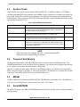
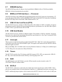
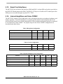
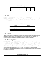
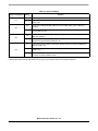
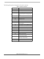
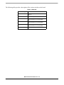
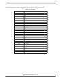
Freescale Semiconductor
Evaluation Board Users Manual
M53015EVBUM
Rev. 0.5, 05/2010
M53015 Evaluation Board
For MCF53015 Evaluation/Validation
by: Microcontroller Division
1
Introduction
The M53015 Evaluation Board (EVB) is based on the V3
ColdeFire Core. This board is shipped with the
MCF53015CMJ240J 256 pin map BGA populated to
allow for the evaluation of the full functionality of this
part.
This board was designed as a validation platform with
maximum flexibility. Where possible we've also
designed for power and speed but the primary goal of this
system was flexibility.
2
Applicable Documents
•
•
MCF53017 Reference Manual
Universal Serial Bus Specification, Revision 2.0
© Freescale Semiconductor, Inc., 2010. All rights reserved.
Contents
1
2
3
4
5
Introduction . . . . . . . . . . . . . . . . . . . . . . . . . . . . . . . . . . . 1
Applicable Documents. . . . . . . . . . . . . . . . . . . . . . . . . . . 1
Evaluation Board Overview . . . . . . . . . . . . . . . . . . . . . . . 2
3.1 Features . . . . . . . . . . . . . . . . . . . . . . . . . . . . . . . . . 2
3.2 EVB Block Diagram . . . . . . . . . . . . . . . . . . . . . . . . . 3
3.3 Board Diagram . . . . . . . . . . . . . . . . . . . . . . . . . . . . 4
Memory Map . . . . . . . . . . . . . . . . . . . . . . . . . . . . . . . . . . 5
Hardware Submodules . . . . . . . . . . . . . . . . . . . . . . . . . . 5
5.1 Processor . . . . . . . . . . . . . . . . . . . . . . . . . . . . . . . . 5
5.2 Reset . . . . . . . . . . . . . . . . . . . . . . . . . . . . . . . . . . . . 5
5.3 System Clocks. . . . . . . . . . . . . . . . . . . . . . . . . . . . . 6
5.4 Program Flash Memory . . . . . . . . . . . . . . . . . . . . . . 6
5.5 MRAM . . . . . . . . . . . . . . . . . . . . . . . . . . . . . . . . . . . 6
5.6 Serial EEPROM. . . . . . . . . . . . . . . . . . . . . . . . . . . . 6
5.7 SDRAM Interface. . . . . . . . . . . . . . . . . . . . . . . . . . . 7
5.8 BDM and JTAG Interfaces — Processor. . . . . . . . . 7
5.9 USB 2.0 Host and Device(OTG) . . . . . . . . . . . . . . . 7
5.10 USB Host Module . . . . . . . . . . . . . . . . . . . . . . . . . . 7
5.11 Interrupts . . . . . . . . . . . . . . . . . . . . . . . . . . . . . . . . . 7
5.12 Timers . . . . . . . . . . . . . . . . . . . . . . . . . . . . . . . . . . . 7
5.13 DSPI . . . . . . . . . . . . . . . . . . . . . . . . . . . . . . . . . . . . 7
5.14 SSI Port . . . . . . . . . . . . . . . . . . . . . . . . . . . . . . . . . . 7
5.15 Smart Card Interfaces . . . . . . . . . . . . . . . . . . . . . . . 8
5.16 Internal Amplifiers and Voice CODEC. . . . . . . . . . . 8
5.17 Ethernet . . . . . . . . . . . . . . . . . . . . . . . . . . . . . . . . . . 9
5.18 UARTs . . . . . . . . . . . . . . . . . . . . . . . . . . . . . . . . . . . 9
5.19 I2C . . . . . . . . . . . . . . . . . . . . . . . . . . . . . . . . . . . . . 10
5.20 eSDHC . . . . . . . . . . . . . . . . . . . . . . . . . . . . . . . . . 10
5.21 Power Regulation . . . . . . . . . . . . . . . . . . . . . . . . . 10
5.22 Boot Options . . . . . . . . . . . . . . . . . . . . . . . . . . . . . 11
5.23 Jumpers, Headers, and Switches . . . . . . . . . . . . . 12
3
Evaluation Board Overview
3.1
Features
The following is a list of evaluation board features.
M53015 External Interfaces:
• On-board speaker (can be connected to on-chip voice CODEC or external on-board audio
CODEC)
• On-board microphone (can be connected to on-chip voice CODEC or external on-board audio
CODEC)
• Synchronous Serial Interface (SSI) connected to on-board audio CODEC
• USB Support
— On-chip dual role transceiver with device, and host, support (Mini-AB receptacle)
• Crystal/Clock
• BDM/JTAG
• Three UARTs; one selectable through Jumper setting
• FlexBus
• Timers
• External Interrupts
• University Breakout Connector for serial interfaces (I2C, QSPI, GPIO, etc.)
• SD card socket
• SIM card socket
• Dual Ethernet
• HDPH, SPKR, HDST, MIC jacks
Memory Subsystems:
• 8M x 16 NOR Flash
• 256K x 16 MRAM
• 2Kbit Serial EEPROM
• 32M x 16 Mobile DDR
Power:
• Inputs:
— 5 V Input to the voltage regulator circuitry
• Regulated On-board voltages:
— 3.3 V - I/O Voltage
— 1.8 V - Mobile DDR and Flash Voltage
— 1.2 V - MCF53015 Core Voltage
M53015 Evaluation Board, Rev. 0.5
2
Freescale Semiconductor
3.2
EVB Block Diagram
Figure 1. EVB Block Diagram
M53015 Evaluation Board, Rev. 0.5
Freescale Semiconductor
3
3.3
Board Diagram
Figure 2. Board Diagram
M53015 Evaluation Board, Rev. 0.5
4
Freescale Semiconductor
4
Memory Map
The M53015EVB contains two FlexBus memory sections. These two nonconsecutive sections were
arranged so that you can easily configure one to support glueless external memories like Flash or SRAM
and configure the other to use as space for unique chip-selects for non-cacheable, non-memory devices
like GPIO, control structures or other I/Os.
In Table 1, you'll find the details on how we've set up the first FlexBus region on the M53015EVB. We
don't set up the second FlexBus memory region.
Table 1. FlexBus Memory Map - Region 1
Component
Start Address
End Address
Size
0x0100_0000
16 MB
0xC008_0000
512 KB
0x4400_0000
64 MB
0x8002_0000
128 KB1
0xFFFF_FFFF
256MB
Flash Memory
Spansion 342-00474
0x0000_0000
MRAM
Everspin MR2A16AYS35
0xC000_0000
SDRAM
Micron MT46H32M16LFCK-75
0x4000_0000
Internal SRAM
Internal
0x8000_0000
Peripheral Space
Internal
0xF000_0000
1
The actual size of the SRAM is 128KByte. However, it may be placed anywhere within the 256MB
space using the RAMBAR register.
5
Hardware Submodules
This section describes the major sections of the M53015EVB.
5.1
Processor
The MCF53015 processor is the fundamental control chip on the M53015EVB. This is a Version 3
ColdFire processor running at a maximum core speed of 240MHz. The M53015EVB allows you to fully
evaluate the feature set of the MCF53015 silicon. Refer to section 3.1 to review the list of board features.
5.2
Reset
Reset can be asserted through a push button switch, SW2. The push button switch is connected to the reset
line on the chip through a Dallas DS1834 Reset chip. Reset of the chip can also be caused by the on-board
BDM circuit, or the University Breakout Connector.
M53015 Evaluation Board, Rev. 0.5
Freescale Semiconductor
5
5.3
System Clocks
Four on-board clock sources are provided on the M53015EVB -- a 20MHz oscillator, a 32.768KHz
oscillator, programmable clock generator, and a 20MHz crystal. Alternatively, an input clock signal can
be provided via an SMA connector for test purposes. The different clock signals and configurations are
described below. Please refer to the MCF53017 Reference Manual for further information on the clocking
requirements for the MCF53015.
Table 2. M53015EVB Clock Definitions
Clock
Description
Frequency
20MHz Input Oscillator
Jumpers J29 and J31 are used to select between clock options. Setting J29
to 2-3 and J31 to 1-2 selects the 20MHz Oscillator option. In this mode, H21
should be populated to pull the XTAL up.
20MHz
20MHz Input Crystal
Setting J31 to 2-3 selects the 20MHz Crystal option. In this mode, H21
should not be populated and the setting of J21 is a don’t care.
20MHz
External Clock Input
Setting J29 to1-2 and J31 to 1-2 selects the External Clock Input option.
The external clock can be input on the SMA connector J46.
Variable
32.768KHz Oscillator
Jumpers J42 and J43 are used to select between Real Time Clock options.
Setting J42 to 2-3 and J43 to 1-2 selects the 32.768KHz Oscillator option
as an input. The default setting for J43 is 2-3 where the processor provides
the 32.768KHz output clock.
Clock Generator
In circuit programmable via the I2C interface.
32.768KHz
Programmable
NOTE
If the clock selection is changed, the SW5-3 switch setting should be
changed to reflect the appropriate clock input.
5.4
Program Flash Memory
The program flash memory on the M53015EVB resides on the first block of FlexBus memory. The
128Mbit Spansion flash can be used for RTOS development. Your software must configure the memory
access parameters consistent with the hardware configuration.
Jumper J33 controls the boot mode of the flash. The default position is 2-3 which selects bottom boot
mode. Setting the jumper to position 1-2, selects top boot mode. This flash device is connected to CS0 and
is the device from which the MCF53015 executes following reset.
5.5
MRAM
512 KB of MRAM are included on the M53015EVB. The MRAM is connected to CS1. The MRAM is a
3.3V part, so level translators are used to interface it to the 1.8V FlexBus.
5.6
Serial EEPROM
The M53015EVB has a 256 KB serial EEPROM connected to the I2C bus that can be used for boot loader
program storage.
M53015 Evaluation Board, Rev. 0.5
6
Freescale Semiconductor
5.7
SDRAM Interface
The M53015EVB provides 64 Mbytes of on-board Mobile SDRAM (16bit x 32M Micron Mobile
SDRAM). On-board terminations are provided.
5.8
BDM and JTAG Interfaces — Processor
The M53015EVB provides a BDM (Background Debug Mode) and JTAG Connector (26-pin header), J37,
to give the end-user the ability to utilize the BDM/JTAG features of the MCF53015 processor. In addition,
the M53015EVB provides an on board USB to BDM interface, J48.
5.9
USB 2.0 Host and Device(OTG)
The MCF53015 Processor contains a USB OTG module. This module is USB 2.0 compliant. It supports
host and device modes, and provides an on-chip full-speed/low-speed transceiver. One mini-AB receptacle
(USB 2.0 OTG) is provided on the M53015EVB.
5.10
USB Host Module
The MCF53015 Processor contains a USB Host module. This module is USB 2.0 compliant. It supports
host mode only, and provides an on-chip full-speed/low-speed transceiver. One Type-A receptacle (USB
2.0 Host) is provided on the M53015EVB.
5.11
Interrupts
There are four external interrupt pins provided on the MCF53015. IRQ7_B is connected to push button
switch SW1 to provide a user driven ABORT signal. This signal is also connected to the LED D5 to denote
when this signal is asserted.
IRQ1_B and IRQ4_B are available on the University Breakout Connector, J1. IRQ6_B is available on pin
2 of J32. IRQ6_B is also used as the USB_CLKIN line.
5.12
Timers
The MCF53015 provides four 32-bit timers with DMA support. DT0 - DT3 are connected to LEDs D1 D4. They can be disconnected from the LEDs by removing jumpers H2 - H5.
5.13
DSPI
The DSPI Module on the MCF53015 is used in SPI bus interface mode to interface with a TI
TLV320AIC23B stereo audio CODEC.
5.14
SSI Port
The MCF53015’s SSI port is connected to the Audio input of the external stereo audio CODEC. These
pins are also available on the University Breakout Connector, J1. Additionally, these pins are muxed with
UART1 and through jumper options, can be connected to an RS232; line driver to be used as UART pins.
M53015 Evaluation Board, Rev. 0.5
Freescale Semiconductor
7
5.15
Smart Card Interfaces
The MCF53015 has two Smart Card interfaces, SIM0 and SIM1. An 8 pin SIM card socket is provided on
the M53015EVB and connected to SIM0. The SIM_P0_VEN pin is accessible on TP5 and the pins of the
SIM1 port are accessible through test points TP6 - TP10.
5.16
Internal Amplifiers and Voice CODEC
The MCF53015 contains a Voice-band audio codec with integrated speaker, microphone, headphone, and
handset amplifiers. The M53015EVB has an on-board speaker and on-board microphone that can be
interfaced to the internal voice CODEC and amplifiers. The microphone and speaker can also be connected
to an external stereo audio CODEC. The jumper setups for the various CODEC configurations are
described in the tables below:
Table 3. Microphone Configuration
Function
J21
J22
J19
J20
Microphone jack connected to internal codec
2-3
2-3
2-3
2-3
Microphone Jack connected to external codec
2-3
2-3
1-2
1-2
Microphone connected to internal codec
1-2
1-2
2-3
2-3
Microphone connected to external codec
1-2
1-2
1-2
1-2
J17
J15
H6
H5
Line In jack connected to internal ADC
1-2
1-2
OFF
OFF
Line In jack connected to external codec in
2-3
2-3
OFF
OFF
Table 4. Line In Configuration
Function
Table 5. Speaker/Headphone Out Configuration
Function
J3
J4
J10
H7
J16
Speaker jack connected to external headphone out
1-2
1-2
OFF
1-2
2-3
Speaker jack connected to internal speaker amp
2-3
2-3
OFF
1-2
2-3
Speaker connected to internal speaker amp
X
X
2-3
X
X
Speaker connected to external headphone out
X
X
1-2
X
X
Speaker jack connected to internal headphone out
X
X
X
OFF
1-2
M53015 Evaluation Board, Rev. 0.5
8
Freescale Semiconductor
Table 6. Headset/Line Out Configuration
5.17
Function
J34
J35
HDSTN/HDSTP lines from internal codec connected
directly to the headset jack
1-2
1-2
DACN/DACP lines from internal codec connected to
the line out jack through filter circuitry
2-3
2-3
LOUT/ROUT lines from external codec connected to
the line out jack through filter circuitry
3-4
3-4
Ethernet
The MCF53015 has 2 10/100 Ethernet MACs. On the M53015EVB these are each connected to National
Semiconductor DP83640 ethernet PHYs. A dual port Ethernet jack, P2, is provided. Ethernet Channel 1 is
connected to the upper port, while Channel 0 is connected to the lower port. Link, speed, and activity lights
are provided for each port. MAC addresses for each Ethernet port are labeled on the board. The DP83640
also supports IEEE 1588. These pins are provided on a 26 pin header, J2.
5.18
UARTs
The MCF53015 includes 3 UART modules. The M53015EVB provides one standard RS232 line driver
necessary to interface with RS232 connectors. This driver is connected to the DB9 connector J52 and
jumper options can connect the driver to either UART1 (muxed with the SSI port pins) or UART2
(dedicated). The board also supplies a USB-to-UART bridge to interface with the MCF53015’s UART0.
If using this option, a USB type B connector can be used to interface with an external device, instead of
the standard RS232 connector. Before using this connector, the Serial to USB bridge driver
“CP210x_VCP_Win2K_XP_S2K3.exe” should be installed. This driver can be found on the included
DVD. Once the driver is installed, the USB port will show up on your computer as a COM port and you
can communicate with it using any terminal program. You can view the Device Manager on your computer
to determine the assigned COM port. UART jumper configurations are described in the following tables:
Table 7. UART1 and UART2 Configuration
Function
J5
J6
J7
J8
J12
J13
Communicate with UART1 through
the DB9 connector J52 (4 pin UART)
1-2
1-2
1-2
1-2
2-3
2-3
Communicate with UART2 through
the DB9 connector J52 (2 pin UART)
X
X
X
X
1-2
1-2
M53015 Evaluation Board, Rev. 0.5
Freescale Semiconductor
9
Table 8. UART0 Configuration
Function
Communicate with UART0 through the Serial to USB
bridge connector, J49
5.19
J44
J45
2-3
2-3
I2C
The I2C bus of the MCF53015 is used in several places on the M53015EVB. It is connected to a serial
EEPROM, a USB OTG Charge Pump, and a programmable clock generator. These pins are also accessible
on the University Breakout Connector, J1. Table 3 below defines the device addresses for the devices
connected to the I2C bus.
Table 9. I2C Device Addresses
Device
5.20
Address
Serial EEPROM
XXX
USB OTG Charge Pump
XXX
Programmable Clock Generator
XXX
eSDHC
The MCF53015 features an Enhanced Secure Digital Host Controller (eSDHC) that supports CE-ATA,
SD Memory, miniSD Memory, SDIO, miniSDIO, SD Combo, MMC, MMC plus, and MMC. The
M53015EVB provides an MMC/SD connector to evaluate the features of the eSDHC.
5.21
Power Regulation
The M53015EVB uses Freescale Switch-Mode power supplies to generate on-board voltages from a single
external 5V supply. The Dual MC34717 generates 1.8V for the memory subsystems and 1.2V to power
the MCF53015 core. The single MC34713 generates 3.3V to power on-board devices. The external 5V
supply is provided through a barrel jack connector, J51. A power switch, SW6, is provided to turn power
to the board off.
Jumpers are provided that allow for the 3.3V, 1.8V, and 1.2V supplies to be separated from the
MCF53015. The intention of these jumpers is to connect a current meter to measure the power consumed
by the MCF53015 processor.
M53015 Evaluation Board, Rev. 0.5
10
Freescale Semiconductor
5.22
Boot Options
The MCF53015 has three boot options:
• Boot from FlexBus with defaults, unified SDR bus/FlexBus
• Boot from FlexBus with defaults, split DDR bus/FlexBus
• Boot from FlexBus and override defaults via address bus (FB_A[21:17])
The boot mode is determined by the BOOTMOD[1:0] inputs into the MCF53015. The mode switches
(SW4[2:1]) control the BOOTMOD[1:0] inputs to the MCF53015.
When booting from FlexBus with overrides from the data bus, the SW6 and SW7 settings control the state
of FB_AD[7:0] during reset (while /RSTOUT is asserted). The following table describes the override
settings.
Table 10. SW3, SW4, and SW5 Settings
Pins Affected
Switch Settings1
Function
SW4-1/SW4-2
Boot Mode
(none)
OFF/OFF
Boot from FlexBus with defaults, unified SDR bus/FlexBus
OFF/ON
Boot from FlexBus with defaults, split DDR bus/FlexBus
ON/OFF
Boot from FlexBus and override defaults via address bus (FB_A[21:17])
ON/ON
Reserved
SW5-1
A16
Master Mode
ON
Master Mode
OFF
Reserved
SW5-2
A17
SDRAM/FlexBus Mode
ON
SDR mode (unified data bus)
OFF
DDR mode (split data bus)
SW5-3
A18
Oscillator Mode
ON
Oscillator bypass mode
OFF
Crystal oscillator mode
SW5-4
A19
Load
ON
High drive strength (50 pF)
OFF
Low drive strength (20 pF)
SW3-1
A20
Boot Port Size
ON
8-bit for split bus or 32-bit for unified bus
OFF
16-bit split or unified bus
M53015 Evaluation Board, Rev. 0.5
Freescale Semiconductor
11
Table 10. SW3, SW4, and SW5 Settings (continued)
Pins Affected
Switch Settings1
Function
SW3-2
Chip Select Configuration
A21
ON
FB_A[23:22] = FB_A[23:22]
OFF
FB_A[23:22] = FB_CS[3:2]
SW3-3
A22
1
Reserved
ON
Reserved
OFF
Default
Bold indicates the default setting, SW4-3, SW4-4, and SW3-4 are not connected and their position does not affect
configuration.
5.23
Jumpers, Headers, and Switches
Headers and jumpers on the M53015EVB allow for user control of the hardware configuration. The
following tables provide descriptions for each of these settings:
Table 11. Header Settings
Reference Designator Setting1,2
Function
ON
Connects a 4 ohm load across the SPKR_N and SPKR_P lines of the internal CODEC
OFF
Disconnects the 4 ohm load across the SPKR_N and SPKR_P lines of the internal CODEC
ON
Connects the T0IN line to the LED D1
OFF
Disconnects the T0IN line from the LED D1
ON
Connects the T1IN line to the LED D2
OFF
Disconnects the T1IN line from the LED D2
ON
Connects the T2IN line to the LED D3
OFF
Disconnects the T2IN line from the LED D3
ON
Connects the T3IN line to the LED D4
OFF
Disconnects the T3IN line from the LED D4
ON
Grounds the ADC_N/MIC_N line of the internal CODEC to AVSS_SPKR_HP_HDST
OFF
Disconnects the ADC_N/MIC_N line of the internal CODEC from AVSS_SPKR_HP_HDST
ON
Connects the Left channel of the Speaker/Headphone Out jack (J18) to the speaker lines
(for speaker use)
OFF
Disconnects the Left channel of the Speaker/Headphone Out jack (J18) from the speaker
lines (for Headphone Out use)
1-2
Adds a 1.0uF capacitor in series with the ADC_N/MIC_N line of the internal CODEC
3-4
Adds a 0.1uF capacitor in series with the ADC_N/MIC_N line of the internal CODEC
5-6
Removes in series capacitance from the ADC_N/MIC_N line of the internal CODEC
H1
H2
H3
H4
H5
H6
H7
H8
M53015 Evaluation Board, Rev. 0.5
12
Freescale Semiconductor
Table 11. Header Settings (continued)
Reference Designator Setting1,2
Function
OFF
Measurement point between the ADC_P/MIC_P and ADC_N/MIC_N lines of the internal
CODEC
ON
Connects the on-board microphone bias voltage divider to VDDE (3.3V)
OFF
Disconnects the on-board microphone bias voltage divider from VDDE (3.3V)
ON
Connects a 16 ohm load to the HP_OUT line of the internal CODEC
OFF
Disconnects the 16 ohm load from the HP_OUT line of the internal CODEC
ON
Current measurement point for the AVDD_SPKR power rail
1-2
Adds a 1.0uF capacitor in series with the ADC_P/MIC_P line of the internal CODEC
3-4
Adds a 0.1uF capacitor in series with the ADC_P/MIC_P line of the internal CODEC
5-6
Removes in series capacitance from the ADC_P/MIC_P line of the internal CODEC
ON
Current measurement point for the AVDD_CODEC power rail
ON
Connects the ADC_P/MIC_P line of the internal CODEC to the microphone circuit (for
Microphone use)
OFF
Disconnects the ADC_P/MIC_P line of the internal CODEC to the microphone circuit (for
Line In use)
ON
Allows for external power input to the Real Time Clock Standby circuit
ON
Grounds the STBY_TEST_MUX signal to GND
OFF
Reserved
ON
Connects an 8 ohm load across the DAC_N/HDST_N and DAC_P/HDST_P lines of the
internal CODEC (for testing purposes)
OFF
Disconnects the 8 ohm load from the DAC_N/HDST_N and DAC_P/HDST_P lines of the
internal CODEC (for Headset or Line Out use)
OFF
Measurement point between the DAC_N/HDST_N and DAC_P/HDST_P lines of the
internal CODEC
ON
Pulls up the XTAL line (for Oscillator bypass mode)
OFF
Disconnects the pullup from the XTAL line (for Crystal Oscillator mode)
ON
Current measurement point for the VDDE power rail
1-2
Puts the Programmable Crystal Oscillator (U14) in Shutdown Mode
3-4
Grounds the S2 line of the Programmable Crystal Oscillator for alternate frequency
operation
H24
ON
Current measurement point for the CVDD power rail
H25
ON
Current measurement point for the SD_VDD power rail
H26
OFF
Test point access for the AVOCOD_ATST_N (pin 1) and AVOCOD_ATST_P lines (pin 2)
ON
Connects the DSPI_PCS3/USB1_VBUS_EN line to the Enable B pin of the USB power
distribution chip (for USB OTG operation)
OFF
Disconnects the DSPI_PCS3/USB1_VBUS_EN line from the Enable B pin of the USB
power distribution chip (for DSPI operation)
H9
H10
H11
H12
H13
H14
H15
H17
H18
H19
H20
H21
H22
H23
H27
M53015 Evaluation Board, Rev. 0.5
Freescale Semiconductor
13
Table 11. Header Settings (continued)
Reference Designator Setting1,2
Function
ON
Connects the power pin of the USB Mini A/B jack, J53, to the Out A pin of the USB power
distribution chip (for Software control of US0 VBUS using USB0_VBUS_EN)
OFF
Disconnects the power pin of the USB Mini A/B jack, J53, from the Out A pin of the USB
power distribution chip (for USB OTG operation controlled by the ID pin of the Mini A/B jack)
ON
Connects the DSPI_PCS2/USB1_VBUS_OC line to the Flag B pin of the USB power
distribution chip (for USB OTG operation)
OFF
Disconnects the DSPI_PCS2/USB1_VBUS_OC line from the Flag B pin of the USB power
distribution chip (for DSPI operation)
ON
Connects a 15K pulldown resistor to the D- line of the USB Host connected to the Type A
socket, J50
OFF
Disconnects the 15K pulldown resistor from the D- line of the USB Host connected to the
Type A socket, J50
ON
Connects a 15K pulldown resistor to the D+ line of the USB Host connected to the Type A
socket, J50
OFF
Disconnects the 15K pulldown resistor from the D+ line of the USB Host connected to the
Type A socket, J50
H28
H29
H30
H31
1
2
Bold indicates the default setting
ON indicates that a shunt should be fitted on the jumper; OFF indicates that no shunt should be applied.
M53015 Evaluation Board, Rev. 0.5
14
Freescale Semiconductor
Table 12. Jumper Settings
Reference Designator Setting1,2
Function
1-2
Connects the LHPOUT line of the external CODEC to the Speaker Out Jack J18
2-3
Connects the SPKR_N line of the internal CODEC to the Speaker Out Jack J18
1-2
Connects the RHPOUT line of the external CODEC to the Speaker Out Jack J18
2-3
Connects the SPKR_P line of the internal CODEC to the Speaker Out Jack J18
1-2
Connects the SSI_RXD/U1_RXD line to the U1RXD line for UART operation
2-3
Connects the SSI_RXD/U1_RXD line to the SSI_RXD line for SSI operation
1-2
Connects the SSI_FS/U1_RTS_B line to the U1RTS_B line for UART operation
2-3
Connects the SSI_FS/U1_RTS_B line to the SSI_FS line for SSI operation
1-2
Connects the SSI_BCLK/U1_CTS_B line to the U1CTS_B line for UART operation
2-3
Connects the SSI_BCLK/U1_CTS_B line to the SSI_BCLK line for SSI operation
1-2
Connects the SSI_TXD/U1_TXD line to the U1TXD line for UART operation
2-3
Connects the SSI_TXD/U1_TXD line to the SSI_TXD line for SSI operation
1-2
Connects the external CODEC to the on-board speaker connected to J9
2-3
Connects the internal CODEC to the on-board speaker connected to J9
1-2
Connects RXD of the RS232 line driver to the UART2 receive line, U2RXD
2-3
Connects RXD of the RS232 line driver to the UART1 receive line, U1RXD
1-2
Connects TXD of the RS232 line driver to the UART2 transmit line, U2TXD
2-3
Connects TXD of the RS232 line driver to the UART1 transmit line, U1TXD
1-2
Connects the ADC_N/MIC_N line of the internal CODEC to the Line In jack, J23
2-3
Connects the CODEC_INR line of the external CODEC to the Line In jack, J23
1-2
Connects the right channel of the Speaker/Headphone Out jack, J18 to the HP_OUT line of
the internal CODEC (for Headphone operation)
J3
J4
J5
J6
J7
J8
J10
J12
J13
J15
J16
2-3
Connects the right channel of the Speaker/Headphone Out jack, J18 to the speaker line (for
Speaker operation)
1-2
Connects the ADC_P/MIC_P line of the internal CODEC to the Line In jack, J23
2-3
Connects the CODEC_INL line of the external CODEC to the Line In jack, J23
1-2
Connects the Mic Bias line to the MIC_BIAS pin of the external CODEC
2-3
Connects the Mic Bias line to the on-boarrd Mic Bias voltage divider circuit
1-2
Connects the Mic In line to the MIC_IN pin of the external CODEC
2-3
Connects the Mic In line to the ADC_P/MIC_P line of the internal CODEC
1-2
Connects the Mic In line to the On-board microphone, P4
2-3
Connects the Mic In line to the Microphone In jack, J25
1-2
Connects the Mic Bias line to the On-board microphone, P4
2-3
Connects the Mic Bias line to the bias circuit of the Microphone In jack, J25
J17
J19
J20
J21
J22
M53015 Evaluation Board, Rev. 0.5
Freescale Semiconductor
15
Table 12. Jumper Settings
Reference Designator Setting1,2
Function
1-2
Connects the RTC_VSTBY_VDD line to H17 (for external power)
2-3
Connects the RTC_VSTBY_VDD line to the on-board super cap circuit
1-2
Sets the PSTCLK/TCLK line to be TCLK (connected to pin 6 of the 26 pin BDM debug
header, J37)
J24
J26
2-3
Sets the PSTCLK/TCLK line to be PSTCLK (connected to pin 24 of the 26 pin BDM debug
header, J37)
1-2
Selects JTAG debug mode
2-3
Selects BDM debug mode
1-2
Pulls up the S2 input of the Zero Delay Clock Buffer, U12
2-3
Reserved
1-2
Selects the SMA connector, J46 as an external clock source for EXTAL
2-3
Selects the 20MHz Oscillator as the clock source for EXTAL
1-2
Selects CPUCLK from the Programmable Clock Generator as the source for EXTAL
2-3
Selects the On-board Oscillator/Crystal/External options as the source for EXTAL
1-2
Selects the Oscillator/External option as a clock source for Extal
2-3
Selects the 20MHz crystal as the clock source between Xtal and Extal
1-2
Connects the 60MHz clock source from the Programmable Clock Generator to the
USB_CLKIN input
J27
J28
J29
J30
J31
J32
2-3
Connects the 24MHz clock source from the Programmable Clock Generator to the
USB_CLKIN input
1-2
Selects Top flash boot mode
2-3
Selects Bottom flash boot mode
1-2
Connects the DAC_N/HDST_N line of the internal CODEC directly to the left channel of the
Headset/Line Out jack, J36 (for Headset operation)
J33
J34
2-3
Connects the DAC_N/HDST_N line of the internal CODEC through filter circuitry to the left
channel of the Headset/Line Out jack, J36 (for Line Out operation)
3-4
Connects the CODEC_OUTL line of the external CODEC through filter circuitry to the left
channel of the Headset/Line Out jack, J36 (for Line Out operation)
1-2
J35
Connects the DAC_P/HDST_P line of the internal CODEC directly to the right channel of
the Headset/Line Out jack, J36 (for Headset operation)
2-3
Connects the DAC_P/HDST_P line of the internal CODEC through filter circuitry to the right
channel of the Headset/Line Out jack, J36 (for Line Out operation)
3-4
Connects the CODEC_OUTR line of the external CODEC through filter circuitry to the right
channel of the Headset/Line Out jack, J36 (for Line Out operation)
1-2
Selects the SMA connector, J47 as an external clock source for XTAL_32K, depending on
the setting of J43
J42
2-3
Selects the on-board 32.768KHz oscillator as the clock source for XTAL_32K, depending
on the setting of J43
M53015 Evaluation Board, Rev. 0.5
16
Freescale Semiconductor
Table 12. Jumper Settings
Reference Designator Setting1,2
J43
Function
1-2
Selects the Oscillator/External option as the external clock source for XTAL_32K
2-3
Selects the on-board 32.768KHz crystal as the clock source between XTAL_32K and
EXTAL_32K
1-2
Connects the U0RTS_B/USB0_VBUS_OC line to USB0_VBUS_OC for USB OTG
operation
J44
2-3
1-2
Connects the U0RTS_B/USB0_VBUS_OC line to U0RTS for UART0 operation through the
serial to USB port, J49
Connects the U0CTS_B/USB0_VBUS_EN/USB_PULLUP line to USB0_VBUS_EN for
USB OTG operation
J45
2-3
1-2
J55
1
2
Connects the U0CTS_B/USB0_VBUS_EN/USB_PULLUP line to U0CTS for UART0
operation through the serial to USB port, J49
Selects the on-board 12MHz crystal as the XTI/XTO input to the external CODEC (for
external CODEC use)
2-3
Selects the SSI_MCLK line as the MCLK input to the external CODEC (for external
CODEC use)
3-4
Connects the CLKOUT line of the external codec to the SSI_MCLK line (Allows the M53015
to monitor the external CODEC clock)
Bold indicates the default setting
ON indicates that a shunt should be fitted on the jumper; OFF indicates that no shunt should be applied.
M53015 Evaluation Board, Rev. 0.5
Freescale Semiconductor
17
The following table provides a description for the interface connectors.
Table 13. Interface Connectors
Reference Designator
Function
J1
University Breakout Connector
J2
IEEE 1588 Connector
J9
On-Board Speaker Connector
J11
Allows multiple chip selects to be used for the
MRAM (not populated, for testing purposes
only)
J18
Speaker/Headphone Out Jack
J23
Line In Jack
J25
Microphone In Jack
J36
Headset/Line Out Jack
J37
BDM Connector
J38
SMA connector for external input of Ethernet
Reference Clock
J39
Logic Analyzer Connector (SDRAM Control)
J40
Logic Analyzer Connector (SDRAM Data)
J41
Logic Analyzer Connector (SDRAM Address)
J46
SMA connector for external input of EXTAL
J47
SMA connector for external input of XTAL_32K
J48
On-board USB to BDM connector
J49
Serial to USB Port
J50
USB Host Type A Socket
J51
Barrel type Power Jack, 5V center positive,
1.93mm center pin diameter
J52
DB9 Socket, connected to UART1 or UART2
depending on jumper settings
J53
USB Mini A/B connector for USB OTG
P4
Microphone
M53015 Evaluation Board, Rev. 0.5
18
Freescale Semiconductor
The following table provides a description of the various switches on the board.
Table 14. Switches
Reference Designator
Function
SW1
Abort Reset push button - Connected to
IRQ7_B
SW2
Board Reset push button
SW3
Board Configuration switch. See Boot
Options section for more information.
SW4
Board Configuration switch. See Boot
Options section for more information.
SW5
Board Configuration switch. See Boot
Options section for more information.
SW6
Power Switch
M53015 Evaluation Board, Rev. 0.5
Freescale Semiconductor
19
The following table provides a description of the various test points on the board.
Table 15. Test Points
Reference Designator
Signal
TP1
GND
TP2
CS_B0
TP3
FB_CLK
TP4
TS_B
TP5
SIM_P0_VEN
TP6
SIM_P1_RST
TP7
SIM_P1_SCLK
TP8
SIM_P1_XMT
TP9
SIM_P1_PD
TP10
SIM_P1_VEN
TP11
HP_OUT
TP12
RW_B
TP13
GND
TP14
OE_B
TP15
RDY
TP16
RESET_B
TP17
SD_SDR_DQS
TP18
RSTOUT_B
TP19
TA_B
TP20
CLKB1 (From Zero Delay Clock Buffer, U12)
TP21
CLKB (From Programmable Clock Generator, U14)
TP22
GND
TP23
GND
M53015 Evaluation Board, Rev. 0.5
20
Freescale Semiconductor