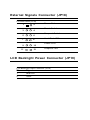
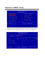
1
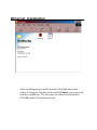
PCM-4898
NS Geode GXLV Media PC board
with LCD, Audio, TV-Output, LAN,
LVDS, 4 COM’s, and 4 bitsD I/O
Copyright Notice
This document is copyrighted, 2000. All rights are reserved. The
original manufacturer reserves the right to make improvements to
the products described in this manual at any time without notice.
No part of this manual may be reproduced, copied, translated or
transmitted in any form or by any means without the prior written
permission of the original manufacturer. Information provided in
this manual is intended to be accurate and reliable. However, the
original manufacturer assumes no responsibility for its use, nor for
any infringements upon the rights of third parties which may result
from its use.
Acknowledgements
VIA is a trademark of VIA Technology, Inc.
AMD is a trademark of Advanced Micro Devices, Inc.
Award is a trademark of Award Software International, Inc.
Cyrix is a trademark of Cyrix Corporation.
IBM, PC/AT, PS/2 and VGA are trademarks of International
Business Machines Corporation.
Intel and Pentium are trademarks of Intel Corporation.
Microsoft Windows ® is a registered trademark of Microsoft Corp.
SMC is a trademark of Standard Microsystems Corporation.
RTL is a trademark of Realtek Semi-Conductor Co., Ltd.
C&T is a trademark of Chips and Technologies, Inc.
UMC is a trademark of United Microelectronics Corporation.
All other product names or trademarks are properties of their
respective owners.
Part No. 2047489800 1st Edition
Printed in Taiwan
October 2000
Packing List
Before you begin installing your card, please make sure that the
following materials are included:
• 1PCM-4898 All-in-one Media GXLV CPU Card
• 1 Quick Installation Guide
• 1 Supporting CD-ROM that contains the following:
•User’s Manual (this manual in PDF file)
•VGA drivers and utilities
•Audio dirvers and utilities
•Latest BIOS (as of the CD-ROM was made)
• 1 hard disk drive (IDE) interface cable (44 pins)
• 1 floppy disk drive interface cable (34 pins)
• 1 Composite output for S-Video connector cable (4 pins)
If any of these items are missing or damaged, contact your
distributor or sales representative immediately.
FCC STATEMENT
THIS DEVICE COMPLIES WITH PART 15 FCC RULES. OPERATION IS SUBJECT TO THE FOLLOWING TWO CONDITIONS:
(1) THIS DEVICE MAY NOT CAUSE HARMFUL INTERFERENCE.
(2) THIS DEVICE MUST ACCEPT ANY INTERFERENCE RECEIVED INCLUDING INTERFERENCE THAT MAY CAUSE
UNDESIRED OPERATION.
THIS EQUIPMENT HAS BEEN TESTED AND FOUND TO
COMPLY WITH THE LIMITS FOR A CLASS "A" DIGITAL
DEVICE, PURSUANT TO PART 15 OF THE FCC RULES.
THESE LIMITS ARE DESIGNED TO PROVIDE REASONABLE
PROTECTION AGAINTST HARMFUL INTERFERENCE WHEN
THE EQUIPMENT IS OPERATED IN A COMMERCIAL ENVIRONMENT. THIS EQUIPMENT GENERATES, USES, AND CAN
RADIATE RADIO FREQENCY ENERGY AND , IF NOT INSTATLLED AND USED IN ACCORDANCE WITH THE INSTRUCTION MANUAL, MAY CAUSE HARMFUL INTERFERENCE TO
RADIO COMMUNICATIONS. OPERATION OF THIS EQUIPMENT IN A RESIDENTIAL AREA IS LIKELY TO CAUSE
HARMFUL INTERFERENCE IN WHICH CASE THE USER WILL
BE REQUIRED TO CORRECT THE INTERFERENCE AT HIS
OWN EXPENSE.
Notice
Dear Customer,
Thank you for purchasing the PCM-4898 board. This user's
manual is designed to assist you in use of our product, please read
it thoroughly before you install and use the board. The product
that you have purchased comes with a two year limited warranty,
however AAEON will not be responsible for misuse of the product.
Therefore, we strongly urge you to read the manual before using
the product.
To receive the lastest version of the user manual, please visit our
Web site at:
http://www.aaeon.com
Contents
Chapter 1: General Information ............................................... 1
Introduction......................................................................2
LVDS Introduction........................................................... 3
Ethernet Introduction.......................................................4
Features .................................................................................. 5
Specifications ......................................................................... 6
Board Demensions ............................................................... 9
Chapter 2: Installation.....................................................10
Jumpers.....................................................................11
Connectors......................................................................12
Locating jumpers ................................................................ 13
Locating connectors ........................................................... 13
Setting jumpers ................................................................... 14
Safety precautions...........................................................15
CPU installing and removing............................................. 15
Installing DRAM (DIMMs) .............................................. 17
ATX power connector (PW 1).........................................18
LVDS connector..............................................................18
IrDA connector...............................................................19
Composite video output connector..............................19
COM 3 (J7) & COM 4 (J8) Serial Port.........................20
Composite output for S-Terminal connector.....................21
CPU ratio connector (JBFA1) ........................................... 21
PCI clock frequency select (JCLK1) .............................. 21
Speaker/Buzzer (JP3).....................................................22
Clear CMOS (JP 1)........................................................22
LCD voltage setting (JP 4)............................................23
Digital I/O connector (JP 5)..........................................24
DiskOnChip (DOC) address selection (JP 6)...............25
CPU fan connector (JP 12).............................................26
CPU core voltage select (JP15)....................................26
COM 2 RS-232/422/485 Selection (JP 16)....................26
LCD backlight power connector (JP19) .......................... 27
External signals connector ...........................................27
Floppy drive connector (CN2) .......................................... 28
Com 1 (CN 3) & Com 2 (CN 4) serial port
[ Dual D-SUB-15P]..........................................................29
USB dual port connector................................................30
Keyboard and mouse connector (CN 6).........................31
Parallel port (CN 7) and VGA connector (J4)................32
Game port (CN 8, D-SUB-9P) &
Connector (CN 10, 11, 13)...............................................33
LCD panel connector (CN 14, header)..........................34
Lan RJ-45 connector (CN 16)........................................35
Primary IDE hard drive connector (CN 1).....................36
Chapter 3: Award BIOS Setup ............................................... 37
Starting setup ....................................................................... 38
Setup keys ............................................................................ 39
Getting help ......................................................................... 40
In case of problem ........................................................... 40
Main setup menu ................................................................ 41
Standard CMOS setup ....................................................... 43
BIOS features setup ........................................................... 49
CHIPSET features setup ................................................... 53
Power management setup .................................................. 55
PNP/PCI congfiguration setup .......................................... 58
Load BIOS defaults/Load setup defaults ........................ 60
Integrated peripherals setup............................................. 61
Supervisor/User password setting ................................... 64
IDE HDD auto detection ................................................... 66
Save & exit setup ................................................................ 67
Exit without saving ............................................................. 68
Chapter 4: DRIVERS INSTALLATION ...................................... 69
Software drives .................................................................... 70
Hardware configuration ...................................................... 70
Necessary prerequisites .................................................... 71
Before you begin ................................................................. 71
Windows 95/98................................................................72
Ethernet (LAN) installation...........................................73
Windows NT 4.0 VGA ........................................................ 76
Windows NT 4.0 audio driver.......................................77
Windows NT 4.0 lan driver.............................................78
Appendix A: Watchdog Timer.........................................79
Watchdog timer programmer..........................................80
CHAPTER
1
General
Information
This chapter gives background information on the PCM-4898.
Sections include:
• Card specifications
• Card layout and dimensions
Introduction
The PCM-4898 is an enhanced, all-in-one single board 486 compuer
with an on-board Ethernet interface, local-bus SVGA controller. The
PCM-4898 offers all the functions of an AT-compatible industrial
computer on a single board, but it fits in the space of a 5¼" floppy
drive (only 5.75" x 8"). For maximum performance, the PCM-4898
also supports 2nd level cache sizes from 128 KB to 512 KB (32 KB x
8, 64 KB x 8, or 128 KB x 8).
On-board features include four serial ports (RS-232 and RS-232/
422/485), one parallel port, an enhanced IDE hard-drive controller
(for up to two drives), a floppy-drive controller and a keyboard/PS/
2 mouse interface. The PCM-4898 is also fitted with a composite
video output connector allowing for easy access to your television.
The board's watchdog timer can automatically reset the system or
generate an interrupt if it stops due to a program bug or EMI
problem.
The PCM-4898 also complies with the "Green Function" standard
and supports three types of power saving features: Doze mode,
Standby mode, and Suspend mode.
All display and Ethernet configuration is done through software. A
single Flash chip holds the system BIOS, VGA BIOS and the
network boot ROM function. This minimizes the number of chips
and eases configuration. You can change the display BIOS or
install a boot ROM simply by programming the Flash chip.
LVDS Introduction
Low Voltage Differential Signaling is a low noise, low power, low amplitude
method for high-speed (gigabits per second) data transmission over
copper wire.
LVDS differs from normal input/output (I/O) in a few ways:
Normal digital I/O works with 5 volts as a high (binary 1) and 0 volts as a
low (binary 0). When you use a differential, you add a third option (-5
volts), which provides an extra level with which to encode and results in a
higher maximum data tranferrate.
A higher data transfer rate means fewer wires are required, as in UW (Ultra
Wide) and UW-2/3 SCSI harddrive, which use only 68 wires. These
devices require a high transfer rate over short distances. Using standard I/
O transfer, SCSI hard drives would require a lot more than 68 wires.
Low voltage means that the standard 5 volts is replaced by either 3.3 volts
or 1.5 volts.
LVDS uses a dual wire system, running 180 degrees of each other. This
enables noise to travel at the same level, which in turn can get filtered
more easily and effectively.
With standard I/0 signaling, data storage is contingent upon the actual
voltage level. Voltage level can be affected by wire length (longer wires
increase resistance, which lowers voltage). But with LVDS, data storage is
distinguished only by positive and negative voltage values, not the
voltage level. Therefore, data can travel over greater lengths of wire while
maintaining a clear and consistent data stream.
Ethernet Introduction
Ethernet is the most popular type of local area network, which sends its
communications through radio frequency signals carried by a coaxial
cable.Each computer checks to see if another computer is transmitting and
waits its turn to transmit. If two computers accidentally transmit at the
same time and their messages collide, they wait and send again in turn.
Software protocols used by Ethernet systems vary, but include Novell
Netware and TCP/IP.
A local-area network (LAN) protocol developed by Xerox Corporation in
cooperation with DEC and Intel in 1976. Ethernet uses a bus or star
topology and supports data transfer rates of 10 Mbps.
A newer version of Ethernet, called 100Base-T (or Fast Ethernet),
supports data transfer rates of 100 Mbps. And the newest version,
Gigabit Ethernet supports data rates of 1 gigabit (1,000 megabits) per
second.
Features
•
Supports NS Media GXLV MMX CPU up to 266 MHz
•
Supports CRT and 18-bit TFT panels
•
Supports TV output (NTSC/PAL)
•
Integrated AC-97 2.0 (meets PC98 ™ Basic Auto spec.)
sound Blaster compatible legacy audio
•
DiskOnChip (SSD) up to 288MB
•
LVDS interface onboard
•
Supports 100Base-T Fast Ethernet
Specifications
CPU type: NS Geode GXLV MMX enhanced Media integrated processor
BIOS: Award 256KB FLASH BIOS
Chipset: Cx5530
I/O Chipset: NS97317/ITE IT8661
Memory: Up to 128MB. One 168-Pin DIMM socket on board.
Enhanced IDE device interface: Supports up to two hard disk drives. BIOS
auto-detect. Supports PIO mode 4 and Bus Master. Also supports Multiword DMA and Ultra DMA/33
Floppy disk drive interface: Supports up to two floppy disk drives, 5.25”
(360KB and 1.2MB) and /or 3.5” (720KB, 1.44MB and 2.88MB)
Parallel port: Configured to LPT1, LPT2, LPT3 or disabled. Supports SPP,
ECP, and EPP.
Serial ports: Three RS-232 and one RS-232/422/485 serial ports. Ports can
be configured as COM1, COM2, COM3, COM4 or disabled
individually.(16C550 equivalent)
IR interface: Supports one IrDA Tx / Rx header
Keyboard/mouse connector: Dual 6-pin mini DIN connector supports PC/
AT keyboard and PS/2 mouse.
USB connector: Dual USB ports on board.
Battery: Lithium battery for data retention of up to 6 years
LVDS Chipset: Thine. THC63LVDM63A
Interface: 20-Pin header for LVDS functions connector
Watchdog timer: Can generate a system reset, IRQ15. Supports Win98,
Win31, Software selectable time-out interval (1~255 sec, 1 sec/step)
DMA channel: 7
Interrupt level: 15TV output
Power management: Supports ATX power supply. Supports PC97 ,
modem ring-in functions. I/O peripheral devices support power saving and
doze/standby/suspend modes. APM 1.2 compliant.
Flat panel/CRT interface
Chipset: NS Cx5530
Display memory: Share memory up to 4MB
Display type: Supports non-interlace CRT and up to 18-bit TFT LCD
displays Can display both CRT and Flat Panel simultaneously.
Resolution: Up to 1280 x 768 @ 64K colors
Chipset: Chrontel 7003 digital PC to TV encoder, supports both PAL and
NTSC.
Interface: On board RCA jack supports NTSC / PAL composite output.
Audio Interface
Chipset: NS Cx5530
Compatible with SoundBlaster, SoundBlaster Pro, and Windows Sound
System.
Ethernet Interface
Chipset: Intel 82559ER
Interface: One standard RJ-45 connector on board supports 100 Base-T
fast Ethernet.
Digital I/O interface
On board 8-pin 2.0mm pin header supports 4-bit input/output TTL
individually.
SSD interface
One 32-pin DIP socket supports M-systems DiskOnChip 2000 series,
memory capacity from 4MB To 288MB.
Expansion Slots
PISA slot: One PISA slot on board for expansion
Mechanical and environment
Power supply : ATX Type
Operating temperature: 32 to 140 °F (0 to 60°C)
Board Size: 200mm(L) x 160mm(W)
Weight: 1.2lb. (0.5Kg)
Board Dimensions
CHAPTER
2
Installation
This chapter tells how to set up the PCM-4898
hardware, including instructions on setting
jumpers and connecting peripherals, switches
and indicators. Be sure to read all the safety
precautions before you begin the installation
procedure.
Jumpers
Name
Function
PW1
ATX Power Connector
J2
IrDA Connector
J3
LVDS Connector
J7 & J8
COM 3 (J7) & COM 4 (J8) Serial Ports
J10
Composite Output For S-Terminal Connector
JCLK1
PCI Clock Frequency Select
JBFA1
CPU Ratio Connector
JP1
Clear CMOS Selection
JP3
Speaker/Buzzer
JP4
LCD Driving Voltage Setting
JP5
Digital I/O Connector
JP6
DiskOnChip(DOC) Address Selection
JP12
CPU Fan Connector
JP15
CPU Core Voltage Select
JP16
COM 2 RS-232/422/485 Selection
JP18
External Signal Connector
JP19
LCD Backlight Power Connector
Connectors
CN2
Floppy Drive Connector
CN3 & CN4
COM 1 (CN3) & COM 2 (CN4) Serial Pports
CN5
USB Dual Port Connector
CN6
Keyboard and Mouse Connector
CN7 & J4
Parallel Port (CN7) & VGA Connector (J4)
CN8
Game Port (D-SUB-15P)
CN13, 10, 11
Audio Connectors
CN14
LCD Panel Connector
CN16
LAN RJ-45 Connector
J1
SDRAM
J4
D-SUB
J6
RCA Jack Composite TV Output
CN10
JP3
CN6
JP18
CN5
Jumper and Connector Locations
JP16
J1
JP12
U1
J3
EISA1
CN16
CN2
CN1
CN4
CN3
JCLK1
JP1
JWOM1
CN7
J2
J4
CN12
CN13
CN8
CN11
JP19
JP15
JBFA1
PW1
CN14
JP4
JP17
J10
J6
JP6
JP5
J8
J7
Setting jumpers
You configure your card to match the needs of your application by
setting jumpers. A jumper is the simplest kind of electric switch. It
consists of two metal pins and a small metal clip (often protected
by a plastic cover) that slides over the pins to connect them. To
“close” a jumper you connect the pins with the clip. To “open” a
jumper you remove the clip. Sometimes a jumper will have three
pins, labeled 1, 2, and 3. In this case you would connect either pins
1 and 2 or 2 and 3.
1
2
3
Open
Closed
Closed 2-3
The jumper settings are schematically depicted in this manual as
follows:
1 2 3
Open
Closed
Closed 2-3
A pair of needle-nose pliers may be helpful when working with
jumpers.
If you have any doubts about the best hardware configuration for
your application, contact your local distributor or sales representative before you make any changes.
Generally, you simply need a jumper to make most connections.
Safety precautions
Warning! Always completely disconnect the power cord
from your chassis whenever you are working on it.
Do not make connections while the power is on
because sensitive electronic components can be
damaged by the sudden rush of power. Only
experienced electronics personnel should open
the PC chassis.
Caution!
Always ground yourself to remove any static
charge before touching the CPU card. Modern
electronic devices are very sensitive to static
electric charges. Use a grounding wrist strap at all
times. Place all electronic components on a
static-dissipative surface or in a static-shielded
bag when they are not in the chassis.
Removing the CPU
The PCM-4898 all-in-one CPU module supports most 486 CPUs.
The system's performance depends on the CPU you choose. You
can install or upgrade the CPU in the board's PGA socket by
following the procedures outlined below. If your system has an
existing CPU, you need to remove it before installing the new CPU.
Removing a CPU
1. Disconnect power from the chassis, and unplug all connections
to the CPU card. Then, remove the CPU card from the chassis
by following the instructions in the user's manual for your
chassis.
2. Lift the CPU out of the PGA socket. The old chip may be
difficult to remove. You may find spray chip lubricant, designed
for pin-grid-array (PGA) devices, and a chip puller helpful.
These are available at electronics hobbyists' supply stores.
Installing A CPU
To install the CPU, follow the instructions that came with it. If no
documentation was provided, the general procedures for installing
a CPU are outlined below:
1. Lubricate the pins on the CPU with lubricant for PGA devices.
This makes the CPU slide in much easier and greatly reduces
the chance of damaging the pins and other components.
2. Carefully align the CPU so that it is parallel to the socket. Make
sure that the notch on the corner of the CPU matches the notch
on the inside of the socket.
3. Gently push the CPU into the socket. There will probably be a
small gap between the CPU and the socket even when it is fully
seated. DO NOT USE EXCESSIVE FORCE!
When you install a new CPU, you may have to adjust other
settings on the board, such as CPU type, CPU clock, and PCI
speed, to accommodate it. Make sure that the settings are correct
for your CPU. Improper settings may damage the CPU.
Installing DRAM (DIMMs)
System Memory
The left edge of the PCM-4898B contains a socket for 168-pin dual
inline memory module (DIMM). The socket uses 3.3 V unbuffered
synchronous DRAM (SDRAM). DIMM is available in capacities of
16, 32, 64, 128, or 256 MB. The socket can be filled in the DIMM of
any size, giving your PCM-4898B single board computer between
16 and 258 MB of memory.
Supplementary information about DIMM
Your PCM-4898B can accept both regular and PC-100 SDRAM
DIMM Module(with or without parity). However. The PCM-4898B
can only accept PC-100 SDRAM Module.
Single-sided modules are typically 16 or 128MB; double-sided
modules are usually 32 or 256 MB.
Memory Installation Procedures
To install SDRAM, first make sure the two handles of the SDRAM
socket are in the "open" position. i.e. The handles remain outward.
Slowly slide the SDRAM module along the plastic guides on both
ends of the socket. Then press the SDRAM module right down
into the socket, until you hear a click. This is when the two handles
have automatically locked the memory module into the correct
position of the SDRAM socket. (See Figure below) To take away
the memory module, just push both handles outward, and the
memory module will be ejected by the mechanism in the socket.
ATX Power Connector (PW1)
On board power input uses a 20-pin standard ATX connector,
the pin definition show as below:
ATX Power Connector (PW1)
Pin
1
Signal
+3.3V
Pin
11
Signal
+3.3V
2
+3.3V
12
-12V
3
GND
13
GND
4
+5V
14
POWER ON
5
GND
15
GND
6
+5V
16
GND
7
GND
17
GND
8
POWER OK
18
-5V
9
+5VSB
19
+5V
10
+12V
20
+5V
LVDS Connector (J3)
PCM-4898 supports one 20-Pin header for LVDS functions
connector. For further details regarding LVDS refer to page 3.
See pin definition below.
LVDS Connector (J3)
Pin
1
Signal
TX 1 +
Pin
11
Signal
TX 2 +
2
TX 1 -
12
TX 2 -
3
GND
13
GND
4
GND
14
GND
5
TXCLK +
15
TX 0 +
6
TXCLK -
16
TX 0 -
7
GND
17
GND
8
PPVCC
18
GND
9
PPVCC
19
GND
10
PPVCC
20
GND
IrDA Connector (J2)
The IrDA connector (J2) can be configured to support wireless
infrared modules. With this module and application software
such as laplink or Win95, Direct Cable connection can
transfer files between laptops, notebooks, PDA and printers.
This connector supports HPSIR ( 115.2Kbps, 2 menters ),
(ASK-IR ( 56Kbps ) and fast IR ( 4Mbps, 2meters ).
Install infrared module onto IrDA connector and enabled
infrared function from BIOS setup, make sure to have correct
orientation when you plug onto IRDA connector(J2).
IrDA connector (J2)
Pin
1
Signal
VCC
2
N/C
3
IRRXD
4
GND
5
IRTXD
6
N/C
Composite video output connector (J6)
The PCM-4898 has a RCA Jack for composite video signal output
to TV.
COM3 (J7) & COM4 (J8) Serial ports
The PCM-4898 offers four serial ports, Three R-S-232 and one R-S232/422/485, those ports allow you to connect them to serial
devices ( mouse, printers, etc.).
COM3 RS-232 (J7)
Pin
1
Signal
SDCDB3X
Pin
2
Signal
SRXDB3
3
STXDB3
4
SDTRB3X
5
GND
6
SDSRB3X
7
SRTSB3X
8
SCTSB3X
9
SRIB3X
10
GND
COM4 RS-232 (J8)
in
1
Signal
SDCDB4X
Pin
2
Signal
SRXDB4
3
STXDB4
4
SDTRB4X
5
GND
6
SDSRB4X
7
SRTSB4X
8
SCTSB4X
9
SRIB4X
10
GND
Composite output for S-terminal
connector (J10)
PCM-4898 supports both RCA and S-terminal signals. The four
pins on (J10) are designated for S-terminal signals because unlike
the RCA signals, S-terminal signals are not supported on board.
Pin
1
Signal
LUMF
2
GND
3
CHROMF
4
GND
PCI Clock Frequency Select (JCLK1)
PCI Clock Frequency Select (JCLK1)
*33MHZ Frequency
1
2
30MHZ Frequency
1
3
2
3
* default
CPU Ratio Connector (JBFA1)
CPU Ratio Connector (JBFA1)
4x
5x
*6x
1
3
5
1
3
5
1
3
5
2
4
7x
6
2
4
8x
6
2
4
9x
6
1
3
5
1
3
5
1
3
5
2
4
10x
6
2
4
6
Reserved
2
4
6
1
3
5
1
3
5
2
4
6
2
4
6
* default
*CPU Clock frequency setting are automatically set by manufacturer.
Clear CMOS selection (JP1)
Users can use JP1 to clear the CMOS data if necessary. To
reset the CMOS data, set J1 to 2-3 closed for just a few
seconds, and then move the jumper back to 1-2 closed.
Clear CMOS selection (JP1)
*Protect
Clear CMOS
* default
Speaker/Buzzer (JP3)
Speaker/Buzzer (JP3)
*On board buzzer
1
*default
2
3
4
External speaker
1
2
3
4
LCD Voltage Setting (JP4)
LCD Panel's Voltage Setting (JP4)
*LCD Panel Power : +5V ; Backlight Power : +5V
1
3
5
2
4
6
LCD Panel Power : +5V ; Backlight Power : +12V
1
3
5
2
4
6
LCD Panel Power : +3.3V ; Backlight Power : +5V
1
3
5
2
4
6
LCD Panel Power : +3.3V ; Backlight Power : +12V
*default
1
3
5
2
4
6
Digital I/O Connector (JP5)
Digital I/O Connector (JP5)
Pin
1
Signal
DATA_IN_0
Pin
2
Signal
DATA_IN_1
3
DATA_IN_2
4
DATA_IN_3
5
DATA_OUT_0
6
DATA_OUT_1
7
DATA_OUT_2
8
DATA_OUT_3
9
VCC
10
GND
DiskOnChip(DOC) Address selection
(JP6)
The DiskOnChip 2000 occupies an 8 Kbyte window in the upper
memory address range of C800 to D400. You should ensure this
does not conflict with any other device's memory address. JP6
controls the memory address of the Flash Disk.
DiskOnChip(DOC) Address selection (JP6)
*D400H
DC00H
5
1
3
5
2
4
6
CE00H
2
4
6
1
5
1
3
5
2
4
6
E000H
2
4
6
1
3
3
D000H
DOC Disable
1
3
5
1
2
4
6
2
D800H
*
3
5
4
6
C800H
1
3
5
1
3
5
2
4
6
2
4
6
Default.
These addresses might conflict with the ROM BIOS of
other peripheral boards, Please select the appropriate
memory address to avoid memory conflicts.
CPU Fan Connector (JP12)
On board offfer a 3-pin wafer for the extenal fan power connection
CPU fan power connector (JP 12)
Pin
1
Signal
N/C
2
+12V
3
Fan speed sense
CPU Core Voltage Select (JP15)
CPU Core Voltage Select (JP15)
*+2.9V
1
2
+2.2V
3
1
2
3
* default
COM2 RS-232/422/485 Selection (JP16)
The PCM-4898 COM2 serial port can be selected as RS-232, RS-422,
or RS-485 by setting JP16.
COM2 R-S232/422/485 selection (JP16)
RS-485
1
2
* default
3
RS-422
1
2
3
*RS-232
1
2
3
External Signals Connector (JP18)
Function Select (JP18)
1
2
3
4
5
6
7
8
9
10
11
12
Power Button
Reset Switch
Suspend Switch
Hard Disk LED
Power LED
Suspend LED
LCD Backlight Power Connector (JP19)
LCD Backlight Power Connector (JP19)
Pin
1
Signal
BLKVCC
2
GND
Floppy Drive Connector (CN2)
Floppy drive connector (CN2)
Pin
1
Signal
GND
Pin
2
Signal
DENSITY SELECT
3
GND
4
N/C
5
GND
6
DRIVE TYPE
7
GND
8
INDEX
9
GND
10
MOTOR 0
11
GND
12
DRIVE SELECT 1
13
GND
14
DRIVE SELECT 2
15
GND
16
MOTOR 1
17
GND
18
DIRECTION
19
GND
20
STEP
21
GND
22
WRITE DATA
23
GND
24
WRITE GATE
25
GND
26
TRACK 0
27
GND
28
WRITE PROTECT
29
GND
30
READ DATA
31
GND
32
HEAD DELECT
33
GND
34
DISK CHANGE
COM1 (CN3) & COM2 (CN4) Serial
Ports [Dual D-SUB-15P]
On board offer four set serial ports for serial devices connection.
Two of them are the D-Sub type, pin definition show as below, for
another two, please refer to page 4.
COM1 RS-232 (CN3) [Down]
Pin
1
Signal
SDCDB1X
Pin
6
Signal
SDSRB1X
2
SRXDB1
7
SRTSB1X
3
STXDB1
8
SCTSB1X
4
SDTRB1X
9
SRIB1X
5
GND
10
GND
Pin
6
Signal
SDSRB2X
COM2 RS-232 (CN4) [Up]
Pin
1
Signal
SDCDB2X
2
SRXDB2
7
SRTSB2X
3
STXDB2
8
SCTSB2X
4
SDTRB2X
9
SRIB2X
5
GND
10
GND
USB Dual Port Connector (CN5)
On board provides two USB interface, which give complete plug
and play, hot attached/detach for up to 127 external devices. The
USB interface comply with USB specification Rev. 1.0, and can be
disable in the system BIOS setup.
USB connector (CN5)
Pin
1
Signal
Vcc
Pin
5
Signal
Vcc
2
USBD1-
6
USBD0-
3
USBD1+
7
USBD0+
4
GND
8
GND
Keyboard and Mouse Connector (CN6)
On board provides two connectors which supports both a
keyboard and a PS/2 style mouse. In most cases, especially
in embedded applications, a keyboard is not used. The
standard PC/AT BIOS will report an error or fail during power
on self test after a reset if the keyboard is not present. The on
board BIOS Advanced setup menu allows you to select
"Present" or "Absent" under the "System Keyboard" section.
This allows no-keyboard operation in embedded system
application without the system halting under POST.
Keyboard and mouse connector (CN6)
Pin
1
Signal
KB DATA
Pin
7
Signal
MS DATA
2
MS DATA
8
N/C
3
GND
9
GND
4
VCC
10
VCC
5
KB CLOCK
11
MS CLOCK
6
MS CLOCK
12
N/C
Parallel Port (CN7) and VGA Connector
(J4)
Normally, the parallel port is used to connect the board to a printer.
The PCM-4898 includes as onboard parallel port with D-Sub type,
and the port is designated as LPT1 and can be disable or change to
LPT2 or LPT3 in the system BIOS setup.
Parallel port (CN7)
Pin
1
Signal
/STB
Pin
2
Signal
D0
3
D1
4
D2
5
D3
6
D4
7
D5
8
D6
9
11
D7
BUSY
10
12
/ACK
PE
13
SLCT
14
/AUTOFD
15
/ERR
16
/INIT
17
/SLCTINI
18
GND
19
GND
20
GND
21
GND
22
GND
23
GND
24
GND
25
GND
26
GND
VGA display connector (J4)
Pin
1
Signal
RED
Pin
9
Signal
VCC
2
GREEN
10
CHASSIS GND
3
BLUE
11
N/C
4
N/C
12
DDDA
5
CHASSIS GND
13
H-SYNC
Game Port (CN8,D-SUB-15P) & Audio
Connectors (CN13,10,11)
Game port connector (CN8) [Up]
Pin
1
Signal
VCC
Pin
9
Signal
VCC
2
JOYF0
10
JOYF2
3
JOYRC0
11
JOYRC2
4
5
GND
GND
12
13
MIDIOUT
JOYRC3
6
JOYRC1
14
JOYF3
7
JOYF1
15
MIDIIN
8
VCC
CN13 : LINE-OUT
CN10 : LINE-IN
CN11: MIC
LCD Panel Connector (CN14)
LCD panel connector (CN14)
Pin
1
Signal
+12 V
Pin
2
Signal
+12 V
3
GND
4
GND
5
LCDVCC
6
LCDVCC
7
ENAVEE
8
GND
9
GND
10
GND
11
P0
12
P1
13
P2
14
P3
15
P4
16
P5
17
19
GND
P6
18
20
GND
P7
21
P8
22
P9
23
P10
24
P11
25
GND
26
GND
27
P12
28
P13
29
P14
30
P15
31
P16
32
P17
33
GND
34
GND
35
SHF CLK
36
FLM(V SYS)
37
M
38
LP (H SYS)
39
GND
40
ENABKL
41
GND
42
N/C
43
LCDVCC
44
LCDVCC
45
GND
46
GND
47
GND
48
GND
49
GND
50
GND
LAN RJ-45 Connector (CN16)
On board supports one standard RJ-45 connector for enthernet
connection. The RJ-45 connector has two LED indicators. Both
LED displays indicate the speed of information being processed,
however the Lan speed does vary.
* The on board Intel 82559XX fast ethernet controller supports
10Mb/s and 100Mb/s N-way auto-negotiation operation.
Green LED : 100M LAN speed,
Yellow LED : 10M LAN speed
RJ-45 Ethernet connector (CN16)
Pin
1
Signal
TX+
Pin
5
Signal
N/C
2
TX-
6
RX-
3
RX+
7
N/C
4
N/C
8
N/C
Primary IDE Hard Drive Connector (CN1)
Primary IDE hard drive connector (CN1)
Pin
1
Signal
IDE RESET
Pin
2
Signal
GND
3
DATA 7
4
DATA 8
5
DATA 6
6
DATA 9
7
DATA 5
8
DATA 10
9
DATA 4
10
DATA 11
11
DATA 3
12
DATA 12
13
DATA 2
14
DATA 13
15
DATA 1
16
DATA 14
17
DATA 0
18
DATA 15
19
GND
20
N/C
21
IDEPDREQR
22
GND
23
IO WRITE
24
GND
25
IO READ
26
GND
27
IO CHANNEL
READY
28
GND
29
IDEPDACKX
30
GND
31
IRQ14
32
IOCS16
33
ADDR 1
34
N/C
35
ADDR 0
36
ADDR 2
37
HARD DISK
SELECT 0
38
HARD DISK SELECT 1
39
IDE ACTIVE
40
MGND
41
VCC
42
VCC
43
GND
44
N/C
CHAPTER
3
Award BIOS Setup
This chapter describes how to configure
the BIOS for the PCM-4898.
Starting setup
The Award BIOS is started immediately when you first turn on the
computer. The BIOS reads, system configuration information in
CMOS RAM and begins the process of checking out the system
and configuring it through the power-on self test (POST).
When these preliminaries are finished, the BIOS seeks an operating
system on one of the data storage devices (hard drive, floppy
drive, etc.). The BIOS launches and hands controls over to the
operating system.
During POST, you can start the Setup program in one of two ways:
1.By pressing Del immediately after switching the system on.
2.By pressing Del or pressing Ctrl-Alt-Esc when the following
message appears briefly at the bottom of the screen during POST:
TO ENTER SETUP BEFORE BOOT PRESS DEL KEY
If the message disappears before you respond and you still wish to
enter Setup. Restart the system again by turning it OFF then ON or
press the RESET button on the system case. You may also restart
by simultaneously pressing Ctr-Alt-Del. If you do not press the
keys at the correct time and the system does not boot, an error
message appears and you are again asked to
PRESS F1 TO CONTINUE, DEL TO ENTER SETUP
Setup keys
These keys helps you navigate in Setup:
Up arrow
Move to previous item
Down arrow
Move to next item
Left arrow
Move to the item in the left hand
Right arrow
Move to the item in the right hand
Esc
Main Menu: Quit and not save
changes into CMOS RAM
Other pages: Exit current page
and return to Main Menu
PgDn/+
Increase the numeric value or
make changes
PgDn/-
Decrease the numeric value or
make changes
F1
General help, only for Status
Page Setup Menu and Option
Page Setup Menu
F2
Change color from total 16 colors.
F2 to select color forward, ShiftF2 to select color backward
F3
Calendar, only for Status Page
Setup Menu
F4
Reserved
F5
Restore the previous CMOS value
from CMOS, only for Option Page
Setup Menu
F6
Load the default CMOS RAM value
from BIOS default table, only for
Option Page Setup Menu
F7
Load the default
F8
Reserved
F9
Reserved
F10
Save all the CMOS changes, only
for Main Menu
Getting help
Press F1 to pop up a small help window. On screen information
describes the appropriate keys to use and the possible selections
for the highlighted item. To exit the Help Window press Esc or the
F1 key again.
In Case of Problems
If, after making and saving system changes with Setup, you
discover that your computer no longer is able to boot. Award BIOS
supports an override to the CMOS settings that resets your system
to its default configuration.
You can invoke this override by immediately pressing Insert; when
you restart your computer. You can restart by either using the ON/
OFF switch, the RESET button or by pressing Ctrl-Alt-Delete.
The best advice is to alter only settings that you thoroughly
understand. In particular, do not change settings in the Chipset
screen without a good reason. The Chipset defaults have been
carefully chosen by Award Software or your system manufacturer
for the best performance and reliability. Even a seemingly small
change to the Chipset setup may cause the system to become
unstable.
Main setup Menu
Standard CMOS
Options in the original PC AT
compatible BIOS.
BIOS Features
Award Software enhanced BIOS
options.
Chipset Features Options specific to your system chipset.
Power
Advanced Power Management (APM)
Management options.
PnP/PCI
Configuration
Plug and Play standard and PCI Local Bus
configuration options.
Integrated
Peripherals
I/O subsystems that depend on the integrated peripherals controller in your
system.
Supervisor/User
Change, set, or disable a password. In
Password Setting BIOS versions that allow separate user and
supervisor passwords, only the supervisor
password permits access to Setup. The
user password generally allows only
power-on access.
IDE HDD Auto
Detection
Automatically detect and configure IDE hard
disk parameters.
Load BIOS
BIOS defaults are factory settings
for the Defaults
most stable,
minimal-performance system
operations.
Load Setup
Setup defaults are factory settings
for Defaults
optimal-performance system operations.
Save & Exit
CMOS
exit Setup.
Save settings in nonvolatile
Setup
RAM and
Exit Without
Setup.
Abandon all changes and exit
Save
Standard CMOS setup
When you choose the STANDARD CMOS SETUP option from the
INITIAL SETUP SCREEN menu, the screen below is displayed.
This standard setup menu allows users to configure system
components such as the date, time, hard disk drive, floppy drive,
display, and memory. Online help for each field can be accessed by
pressing F1.
Date and Time Configuration
The BIOS determines the day of the week from the other date
information. This field is for information only.
Press the left or right arrow key to move to the desired field (date,
month, year). Press the PgUp/- or PgDn/+ key to increment the
setting, or type the desired value into the field.
The time format is based on the 24-hour military-time clock. For
example, 1 p.m. is 13:00:00 hours. Press the left or right arrow key to
move to the desired field. Press the PgUp/- or PgDn/+ key to
increment the setting, or type the desired value into the field.
HARD DISKS
The BIOS supports up to four IDE drives. This section does not
show information about other IDE devices, such as a CD-ROM
drive, or about other hard drive types, such as SCSI drives.
NOTE: We recommend that you select type AUTO for all drives.
The BIOS can automatically detect the specifications and optimal
operating mode of almost all IDE hard drives. When you select
type AUTO for a hard drive, the BIOS detects its specifications
during POST, every time the system boots.
If you do not want to select drive type AUTO, other methods of
selecting the drive type are available:
1.Match the specifications of your installed IDE hard drive(s) with
the preprogrammed values for drive types 1 through 45.
2.Select USER and enter values into each drive parameter field.
3.Use the IDE HDD AUTO DECTECTION function in Setup.
Here is a brief explanation of drive specifications:
•Type: The BIOS contains a table of pre-defined drive types. Each
defined drive type has a specified number of cylinders,
number of heads, write precompensation factor, landing
zone, and number of sectors. Drives whose specifications
do not accommodate any pre-defined type are classified as
type USER.
•Size: Disk drive capacity (approximate). Note that this size is
usually slightly greater than the size of a formatted disk
given by a disk-checking program.
• Cyls: Number of cylinders
• Head: Number of heads
• Precomp: Write precompensation cylinder
• Landz: Landing zone
• Sector: Number of sectors
• Mode: Auto, Normal, Large, or LBA
- Auto: The BIOS automatically determines the optimal mode.
- Normal: Maximum number of cylinders, heads, and sectors
supported are 1024, 16, and 63.
- Large: For drives that do not support LBA and have more than
1024 cylinders.
- LBA (Logical Block Addressing): During drive access, the
IDE controller transforms the data address described by
sector, head, and cylinder number into a physical block
address, significantly improving data transfer rates. For
drives with greater than 1024 cylinders.
Drive A
Drive B
Select the correct specifications for the diskette drive(s) installed in
the computer.
None
No diskette drive installed
360K, 5.25 in
5-1/4 inch PC-type standard drive;
360 kilobyte capacity
1.2M, 5.25 in
5-1/4 inch AT-type high-density
drive; 1.2 megabyte capacity
720K, 3.5 in
3-1/2 inch double-sided drive;
720 kilobyte capacity
1.44M, 3.5 in
3-1/2 inch double-sided drive;
1.44 mega byte capacity
2.88M, 3.5 in
3-1/2 inch double-sided drive;
2.88 mega byte capacity
Halt On
During the power-on-self-test (POST), the computer stops if the
BIOS detects a hardware error. You can tell the BIOS to ignore
certain errors during POST and continue the boot-up process.
These are the selections:
• No errors: POST does not stop for any errors.
• All errors If: the BIOS detects any non-fatal error, POST stops
and prompts you to take corrective action.
• All, But Keyboard: POST does not stop for a keyboard error, but
stops for all other errors
• All, But Diskette: POST does not stop for diskette drive errors,
but stops for all other errors.
• All, But Disk/Key: POST does not stop for a keyboard or disk
error, but stops for all other errors.
Memory
You cannot change any values in the Memory fields; they are only
for your information. The fields show the total installed random
access memory (RAM) and amounts allocated to base memory,
extended memory, and other (high) memory. RAM is counted in
kilobytes (KB: approximately one thousand bytes) and megabytes
(MB: approximately one million bytes).
RAM is the computer's working memory, where the computer
stores programs and data currently being used, so they are
accessible to the CPU. Modern personal computers may contain up
to 64 MB, 128 MB, or more.
•Base Memory
Typically 640 KB. Also called conventional memory. The DOS
operating system and conventional applications use this area.
•Extended Memory
Above the 1-MB boundary. Early IBM personal computers could
not use memory above 1 MB, but current PCs and their software
can use extended memory.
•Other Memory
Between 640 KB and 1 MB; often called High memory. DOS may
load, terminate-and-stay-resident (TSR) programs, such as device
drivers, in this area, to free as much conventional memory as
possible for applications. Lines in your CONFIG.SYS file that start
with LOADHIGH, load programs into high memory.
BIOS features setup
By choosing the BIOS FEATURES SETUP option from the INITIAL
SETUP SCREEN menu, the screen below is displayed.
The displayed configuration is based on the manufacturer's SETUP
DEFAULTS settings.
Virus Warning
When enabled, you receive a warning message if a program
(specifically, a virus) attempts to write to the boot sector or the
partition table of the hard disk drive. You should then run an antivirus program. Keep in mind that this feature protects only the boot
sector, not the entire hard drive.
NOTE: Many disk diagnostic programs that access the boot
sector table can trigger the virus warning message. If you plan to
run such a program, we recommend that you first disable the virus
warning.
CPU Internal Cache/External Cache
Cache memory is additional memory that is much faster than
conventional DRAM (system memory). CPUs from 486-type on up
contain internal cache memory, and most, but not all, modern PCs
have additional (external) cache memory. When the CPU requests
data, the system transfers the requested data from the main DRAM
into cache memory, for even faster access by the CPU.
The External Cache field may not appear if your system does not
have external cache memory.
Quick Power On Self Test
Select Enabled to reduce the amount of time required to run the
power-on-self-test (POST). A quick POST skips certain steps. We
recommend that you normally disable quick POST. Better to find a
problem during POST than lose data during your work.
Boot Sequence
The original IBM PCs loaded the DOS operating system from drive
A (floppy disk), so IBM PC-compatible systems are designed to
search for an operating system first on drive A, and then on drive C
(hard disk). However, the BIOS now offers many boot sequence
options.
Swap Floppy Drive
This field is effective only in systems with two floppy drives.
Selecting enabled assigns physical drive B to logical drive A, and
physical drive A to logical drive B.
Boot Up Floppy Seek
When Enabled, the BIOS tests (seeks) floppy drives to determine
whether they have 40 or 80 tracks. Only 360-KB floppy drives have
40 tracks; drives with 720 KB, 1.2 MB, and 1.44 MB capacity all
have 80 tracks. Because very few modern PCs have 40-track floppy
drives, we recommend that you set this field to Disabled to save
time.
Boot Up NumLock Status
Toggle between On or Off to control the state of the NumLock key
when the system boots. When toggled On, the numeric keypad
generates numbers instead of controlling cursor operations.
Gate A20 Option
Gate A20 refers to the way the system addresses memory above 1
MB (extended memory). When set to Fast, the system chipset
controls Gate A20. When set to Normal, a pin in the keyboard
controller controls Gate A20. Setting Gate A20 to Fast improves
system speed, particularly with OS/2 and Windows.
Security Option
If you have set a password, select whether the password is
required every time the System boots, or only when you enter
Setup.
Shadow
Software that resides in a read-only memory (ROM) chip on a
device is called firmware. The AwardBIOS permits shadowing of
firmware such as the system BIOS, video BIOS, and similar operating instructions that come with some expansion peripherals, such
as, for example, a SCSI adaptor.
Shadowing copies firmware from ROM into system RAM, where
the CPU can read it through the 16-bit or 32-bit DRAM bus.
Firmware not shadowed must be read by the system through the 8bit X-bus. Shadowing improves the performance of the system
BIOS and similar ROM firmware for expansion peripherals, but it
also reduces the amount of high memory (640 KB to 1 MB) available for loading device drivers, etc.
Enable shadowing into each section of memory separately. Many
system designers hardwire shadowing of the system BIOS and
eliminate a System BIOS Shadow option.
Video BIOS shadows into memory area C0000-C7FFF. The remaining areas shown on the BIOS Features Setup screen may be
occupied by other expansion card firmware. If an expansion
peripheral in your system contains ROM-based firmware, you need
to know the address range the ROM occupies to shadow it into the
correct area of RAM.
Cyrix 6x86/MII CPU-ID
CPU identification is the personal identity or fingerprint of your
CPU. Every computer or CPU driven device has this fuction. This
information provides the end user with the type and speed of the
CPU. The CPU identification is shown on screen everytime you
boot your computer.
• Enable CPU-ID will allow you the end user to view your CPU
identification number everytime you boot your computer.
• Disable CPU-ID will not allow you the end user to view your CPU
identification number when you boot your computer, however this allows
your computer the ability to boot faster because the computer has one less
task to run.
CHIPSET features setup
By choosing the CHIPSET FEATURES SETUP option from the
INITIAL SETUP SCREEN menu, the screen below is displayed.
The displayed configuration is based on the manufacturer's SETUP
DEFAULTS settings.
This section allows you to configure the system based on the
specific features of the installed chipset. This chipset manages bus
speeds and access to system memory resources, such as SDRAM.
It also coordinates communications between the conventional ISA
bus and the PCI bus. It must be stated that these items should
never need to be altered. The default settings have been chosen
because they provide the best operating conditions for your
system. The only time you might consider making any changes
would be if you discovered that data was being lost while using
your system.
Because of the complexity and technical nature of some of the
options, not all of the options are described here.
SDRAM CAS Latency Time
When synchronous DRAM is installed, you can control the
number of CLKs between when the SDRAMs sample a read
command and when the contoller samples read data from the
SDRAMs. Do not reset this field from the default value specified
by the system designer.
8/16 Bit I/O Recovery Time
The I/O recovery mechanism adds bus clock cycles between PCIoriginated I/O cycles to the ISA bus. This delay takes place
because the PCI bus is so much faster than the ISA bus.
These two fields let you add recovery time (in bus clock cycles) for
16-bit and 8-bit I/O.
Power management setup
By choosing the POWER MANAGEMENT option from the
INITIAL SETUP SCREEN menu, the screen below is displayed.
Power Management
This option allows you to select the type (or degree) of power
saving for Doze, Standby, and Suspend modes.
This table describes each power management mode:
Max Saving
Maximum power savings. Only
Available for SL CPUs. Inactivity
period is 1 minute in each mode.
User Define
Set each mode individually.
Select time-out periods in the
section for each mode, below.
Min Saving
Minimum power savings. Inactivity
period is1 hour in each mode
(except the hard drive).
Doze Mode
After the selected period of system inactivity, the CPU clock
throttles to a small percentage of its duty cycle — between 10
percent and 25 percent for most chipsets. All other devices still
operate at full speed.
Standby mode
After the selected period of system inactivity, the CPU clock stops,
the board drive enters an idle state, and the L2 cache enters a
power-save mode. All other devices still operate at full speed.
HDD Power Down
After the selected period of drive inactivity, any system IDE
devices compatible with the ATA-2 specification or later power
manage themselves, putting themselves into an idle state after the
specified timeout and then waking themselves up when accessed.
MODEM Use IRQ
Name the interrupt request (IRQ) line assigned to the modem (if
any) on your system. Activity of the selected IRQ always awakens
the system.
Throttle Duty Cycle
When the system enters Doze mode, the CPU clock runs only part
of the time. You may select the percent of time that the clock runs.
PNP/PCI configuration setup
By choosing the PNP/PCI CONFIGURATION SETUP option from
the initial SETUP SCREEN menu, the screen below is displayed.
PNP OS Installed
Select Yes if the system operating environment is Plug-and-Play
aware (e.g., Windows 95).
Resources Controlled By
The Plug and Play AwardBIOS can automatically configure all the
boot and Plug and Play-compatible devices. If you select Auto, all
the interrupt request (IRQ) and DMA assignment fields disappear,
as the BIOS automatically assigns them.
Reset Configuration Data
Normally, you leave this field Disabled. Select Enabled to reset
Extended System Configuration Data (ESCD) when you exit Setup if
you have installed a new add-on and the system reconfiguration
has caused such a serious conflict that the operating system
cannot boot.
PCI IRQ Activated by
Leave the IRQ trigger set at Level unless the PCI device assigned
to the interrupt specifies Edge-triggered interrupts.
Load BIOS defaults/Load setup
defaults
LOAD BIOS DEFAULTS loads the default system values directly
from ROM. The BIOS DEFAULTS provides the most stable
settings, though they do not provide optimal performance. LOAD
SETUP DEFAULTS, on the other hand, provides for maximum
system performance. If the stored record created by the setup
utility becomes corrupted (and therefore unusable), BIOS defaults
will load automatically when you turn the PCM-4897 on.
Integrated peripherals setup
By choosing the INTEGRATD PERIPHERALS option from the
initial SETUP SCREEN menu, the screen below is displayed.
IDE HDD Block Mode
Select Enabled only if your hard drives support block mode.
IDE PIO Modes (Primary Master/Slave)
The four IDE PIO (Programmed Input/Output) fields let you set a
PIO mode (0-4) for each of up to four IDE devices that the internal
PCI IDE interface supports. Modes 0 through 4 provide successively increased performance. In Auto mode, the system automatically determines the best mode for each device.
IDE Primary Master/Slave UDMA
UDMA (Ultra DMA) is a DMA data transfer protocol that utilizes
ATA commands and the ATA bus to allow DMA commands to
transfer data at a maximum burst rate of 33 MB/s. When you select
Auto in the four IDE UDMA fields (for each of up to four IDE
devices that the internal PCI IDE interface supports), the system
automatically determines the optimal data transfer rate for each IDE
device.
RING POWER ON Controller
Onboard FDC Controller
Select Enabled if your system has a floppy disk controller (FDC)
installed on the system board and you wish to use it. If you install
an add-in FDC or the system has no floppy drive, select Disabled in
this field.
Onboard Serial Ports (1, 2, 3, 4)
Normally, the main board’s I/O chips will occupy a certain portion
of memory space. For each I/O device the computer provides an
I/O address. The more devices attached the more address needed
to organize the memory storage areas. If all the I/O devices were
run through the same address, your devices would come to a near
halt. By providing the end user with four serial ports this allows
devices to run more efficiently if needed.
Selections of logical COM port addresses are as follows. ( 3F8H,
3E8H, 2F8H, 2E8H)
ECP Mode Use DMA
Select a DMA channel for the port.
Multiple Monitor Support
Choose priority of the VGA function from PCI slot or onboard.
Video Memory size
Share memory from DIMM, from 1.5MB to 4MB.
TV Output mode
Support NTSC or PAL system.
Flat Panel Resolution
Onboard support TFT LCD as below.
640x480
800x600
1024x768
Supervisor/User password setting
You can set either SUPERVISOR or USER PASSWORD, or both of
them. The difference between the two is that the supervisor
password allows unrestricted access to enter and change the
options of the setup menus, while the user password only allows
entry to the program, but not modify options.
When you select this function, a message appears at the center of
the screen:
ENTER PASSWORD:
Type the password, up to eight characters, and press Enter. Typing
a password clears any previously entered password from CMOS
memory.
Now the message changes:
CONFIRM PASSWORD:
Again, type the password and press Enter.
To abort the process at any time, press Esc.
In the Security Option item in the BIOS Features Setup screen,
select System or Setup:
System Enter a password each time the system boots and when
ever you enter Setup.
Setup
Enter a password when ever you enter Setup.
NOTE: To clear the password, simply press Enter when asked to
enter a password. Then the password function is disabled.
IDE HDD auto detection
The IDE HDD AUTO DETECTION utility can automatically detect
the IDE hard disk installed in your system. You can use it to selfdetect and/or correct the hard disk type configuration. You need to
repeat the setup for each of the IDE combinations:
Save & exit setup
If you select this option and press <ENTER>, the values entered in
the setup utility will be recorded in the chipset's CMOS memory.
The microprocessor will check this every time you turn your
system on and compare this to what it finds as it checks the
system. This record is required for the system to operate.
Exit without saving
If you select this option and press <ENTER>, the values entered in
the setup utility will be recorded in the chipset's CMOS memory.
The microprocessor will check this every time you turn your
system on and compare this to what it finds as it checks the
system. This record is required for the system to operate.
CHAPTER
4
DRIVERS INSTALLATION
• AUDIO
This PCM-4898 is equipped with an audio
interface that records and playback
CD-quality audio. This chapter provides
instructions for installing the software
drivers on the included CDROM.
• ETHERNET
Intel 82559 Ethernet Mux
Driver for VxWorks *5.3.1/5.4 Installation
Software drivers
This chapter describes the operation and installation of the display
drivers supplied on the Supporting CD-ROM that are shipped with
your product.
The onboard VGA adapter is based on the Cx5530 VGA Flat Panel/CRT
controller. This controller offers a large set of extended functions and
higher resolutions. If you intend to use your VGA adapter in standard
VGA modes only, you do not need to install any of these drivers. Since
your VGA adapter is fully compatible, it does not require any special
drivers to operate in standard modes.
The purpose of the enclosed software drivers is to take advantage of
the extended features of the CHIPS VGA Flat Panel/CRT controller.
Hardware configuration
Some of the high-resolution drivers provided in this package will work
only in certain system configurations. If a driver does not display
correctly, try the following:
1. Change the display controller to CRT-only mode, rather than flat
panel or simultaneous display mode. Some high-resolution drivers
will display correctly only in CRT mode.
2. If a high-resolution mode is not supported on your system, try
using a lower-resolution mode. For example, 1024 x 768 mode will
not work on some systems, but 800 x 600 mode is supported on
most.
Necessary prerequisites
The instructions in this manual assume that you understand
elementary concepts of MS-DOS and the IBM Personal Computer.
Before you attempt to install any driver from the Supporting CDROM, you should:
• Know how to copy files from a CD-ROM to a directory on the
hard disk
• Understand the MS-DOS directory structure
If you are uncertain about any of these concepts, please refer to
the DOS or OS/2 user reference guides for more information before
you proceed with the installation.
Before you begin
Make sure you know the version of the application for which you
are installing drivers. The Supporting CD-ROM contain drivers for
several versions of certain applications. For your driver to operate
properly, you must install the driver for your version of the
application program.
Windows 95/98
Installing VGA and Audio Driver
PCM-4898 has a built in CX 5530 chipset that offers VGA and
Audio interface. The installation for VGA and Audio are
automatic. Simply, install the provided CD into the CD-ROM drive
and select, my computer. Click on the CD-ROM drive in the
opened window. Find the VGA and Audio file named Cyrix Media
GX Certified Win9x Driver 4.0, and double click on the file. The
file will open up and offer a set up wizard. Follow the instructions
and click on the corresponding buttons and the VGA and Audio
features will self install. Shutdown afterwards to ensure proper
installation.
Installing Lan Driver
First you must unzip the Lan Intel 82559ER file on the CD-ROM. If
the file is already unzipped, proceed with the installtion. There are
two main files needed for installation b559mux and d559vx.
Choose and click on my computer, from there select your CD-ROM
drive. Find the two file names from above and select enter. The
following three pages show installation directions. Follow the
same steps for both files and your LAN driver will have been
installed. Shut down afterwards to ensure proper installation.
Ethernet Installation
After installing the provided CD in the CD-ROM player this
widow will appear. Double click on the b559mus icon to proceed
with the installation. The file name for ethernet installation is
82559ER, in the 82559erdrivers16.zip.
Ethernet Installation
This window is asking for a folder location on your computer to
save this new Ethernet download. In this situation the
preselected folder is the C:folder. If you choose to change the
folder location simple double click the Browse icon and make
your selection. To proceed with the installation, simply double
click on the Finish icon.
Ethernet Installation
This is the final step in the Ethernet installation. Simply double
click on the YES icon to finalize the installation.
Windows® NT 4.0
VGA Driver
Driver installation
1. Install WindowsÒ NT 4.0 as you normally would for a VGA
display. Click the Start buttom, go to Settings and click on
Control Panel icon. Then choose the Display and double click on
the icon. In the Display Properties window, click the Setting
buttom, then click the Display Type buttom into the Display Type
windows, then click on Change buttom from the Adapter Type icon.
And click on Have Disk buttom in the change display window.
2. Place the Supporting CD-ROM into the CD-ROM drive. In the
Select Device window, click on Have Disk, select "Browse" and
find the NT 4.0 driver from:
cd-rom : \CD ROM\model name\dirver\vga driver\win98
nt\windows.nt\nt40\Oemsetup.inf
"cd-rom" : the drive letter of your CD-ROM drive
"model name" : the model number of your product
and then click OK. The name of the CCryix Xpress
GRAPHICS(TM) driver will appear highlighted in the Modules list
box. Select Gx5530 and Click OK. Click OK to start the driver
installation.
3. Once the installation is complete, the Change Display Type window
will reappear. Click on close to close the window. Then the
Display Properties window will reappear. Click on Apply. Restart
the system for the new settings to take effect.
4. There are five files ( gx.dll, gx.sys, gx.inf, gx.vid, license.pdf) in the
Windows NT 4.0 system.
Windows® NT 4.0
Audio Driver
Driver installation
*Must Disable the MPU-401 function first, In your
BIOS*
1. Install WindowsÒ NT 4.0 as you normally would for a Audio driver
display. Click the Start button, go to Settings and click on Control
Panel icon. Then choose the multimedia and double click on the
icon. In the Multimedia window, click the device button, then click
the add button in the device window. Select the unlisted or updated
driver, then click on the OK button. The next window will ask for a
specific drive location and file name. The audio driver will be found
in the CD-ROM player under the Audio section. After you have
found the location of your audio drive, click OK.
2. Place the Supporting CD-ROM into your CD-ROM dirve. In the
Select Device window, click on Have Disk, select "Browse" and
find the NT 4.0 driver from:
cd-rom : \CD ROM\model name\dirver\audio driver\win98
nt\windows.nt\nt40\Oemsetup.inf
"cd-rom" : the drive letter of your CD-ROM drive
"model name" : the model number of your product
Once you have found the audio driver, click OK. Next an add
unlisted or updated driver window will appear, there will be a
message reading National Xpress Audio (TM) Driver, click OK.
AN I/O window will appear next asking for the address number,
type in 220 and click on the continue button. The very next
window is the Xpress Audio Configuration window. In the bottom
of the page there is a MPU 401 I/O Address, select the disable
function and click OK.
The audio driver has been installed please restart your system.
Windows® NT 4.0
Lan Driver
Driver installation
1. Install WindowsÒ NT 4.0 as you normally would for a Lan driver
display. Click the Start buttom, go to Settings and click on
Control Panel icon. Then choose the Network and double click on
the icon. In the Network window, click the Yes, want to install
button. Then a wired to network window will appearclick the Next
button. A select from list window will then appear click on the
choose from disk option. Once the address has been found on the
CD-ROM address click OK.
2. Place the Supporting CD-ROM into your CD-ROM drive. The file
name can be found under the Driver section on the CD-ROM.
cd-rom : \CD ROM\model name\dirver\lan driver\win98
nt\windows.nt\nt40\Oemsetup.inf
"cd-rom" : the drive letter of your CD-ROM drive
"model name" : the model number of your product
and then click OK.
In the next widow INTEL (R) GD82559ER Evaluation Adapter will
appear, click OK.
The next window will be asking for Network Protocal information
select the desired options and click, next.
3. Once the installation is complete, check under the Network windows in the control panel option to verify your LAN driver has
been installed.
APPENDIX
A
Programming the
Watchdog Timer
The PCM-4898 is equipped with a
watchdog timer that resets the CPU or
generates an interrupt if processing comes
to a standstill for whatever reason. This
feature ensures system reliability in
industrial standalone, or unmanned,
environments.
Programming the watchdog timer
Watchdog timer
The watchdog timer uses a EPLD (erasable programmable logical
device) to program the WatchDog function. The time range is from
1 second to 255 seconds. When timer times out, a system reset will
happen.
Configuration register
The watchdog timer of PCM-4898 is located in a IC on the board. If
you want to use it, you have to know how to reset the timer. The
procedure is as follows.
Use the debug (DOS command) under DOS
-O 443 5
==> set 5 seconds
-O 444 0
==> set watchdog reset function
It means that it will reset after it counts 5 seconds
-O 443 FF
==> set the maximum, 255 seconds
-O 443 2
==> it will occur IRQ15 pulse
It means that it will have a IRQ 15 pulse after 255 seconds
The IRQ (interrupt request) value is an assigned location where
the computer can expect a particular device to interrupt it when
the device sends the computer signals about its operation. For
example, when a printer has finished printing, it sends an
interrupt signal to the computer. The signal momentarily interrupts the computer so that it can decide what processing to do
next. Since multiple signals to the computer on the same interrupt
line might not be understood by the computer, a unique value
must be specified for each device and its path to the computer.