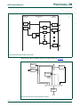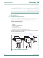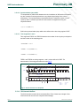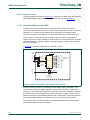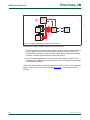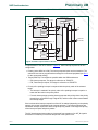
1
D
D
D
D
D
A
A
A
A
A
FT
FT
FT
FT
FT
D
R
R
A
A
FT
FT
FT
FT
A
A
R
R
D
D
D
D
R
R
A
FT
FT
FT
A
A
R
R
D
D
D
LPC2917/19 - ARM9 microcontroller with CAN and LIN
R
A
F
FT
FT
A
A
R
R
D
D
User manual
D
Rev. 01.02. — 8 November 2007
R
R
R
R
R
Preliminary UM
D
FT
FT
A
A
R
R
D
D
D
R
A
FT
D
R
A
Document information
Info
Content
Keywords
LPC2917/19, User Manual, ARM9, CAN, LIN, Gateway
Abstract
This document extends the LPC2917/19 data sheet with additional details
to support both hardware and software development. It focuses on
functional description and typical application use.
D
D
D
D
D
R
R
R
R
R
D
R
R
FT
D
R
FT
FT
A
A
R
D
D
R
A
FT
D
R
starting address of static memory bank address corrected, see Table 27.
A
01
20071003
•
•
•
Use of RBLE-bit in SMBCRn-register updated, see Table 34.
Register base address table updated, see Table 3.
20070913
Initial version
Contact information
For additional information, please visit: http://www.nxp.com
For sales office addresses, please send an email to: [email protected]
UMxxxxx
User manual
F
D
D
Modifications:
A
FT
FT
A
A
R
R
R
Modifications: Removed part LPC2915
01.01
R
A
D
D
20071108
D
R
FT
FT
A
A
R
R
D
D
D
01.02
Description
FT
FT
FT
FT
Date
A
A
A
A
R
R
D
D
D
Revision history
FT
FT
FT
FT
FT
LPC2917/19 - ARM9 microcontroller with CAN and LIN
Rev
A
A
A
A
A
Preliminary UM
NXP Semiconductors
© NXP B.V. 2007. All rights reserved.
Rev. 01.02. — 8 November 2007
2 of 263
D
D
D
D
D
R
R
R
R
R
A
A
A
A
A
D
R
R
FT
FT
FT
FT
D
R
R
A
FT
FT
FT
A
A
R
R
D
D
D
R
A
F
FT
FT
A
A
R
R
D
D
D
D
FT
FT
A
A
R
R
D
1.1 About this document
A
A
A
A
R
R
D
D
D
LPC2917/19 - ARM9 microcontroller with CAN and LIN
1. Introduction
FT
FT
FT
FT
FT
Preliminary UM
NXP Semiconductors
D
D
R
A
An overview of the functionality of the LPC2917/19 is given as well as a functional
description of the blocks and their typical usage. Register descriptions are given in the
appropriate sub-sections. The Datasheet Ref. 1 should be used along with this document.
2. Overview
This chapter gives an overview of the functional blocks, clock domains, power modes and
the interrupt and wake-up structure.
2.1 Functional blocks and clock domains
Figure 1 gives a simplified overview of the functional blocks. These blocks are explained
in detail in Section 3 (with the exception of some trivial blocks). Several blocks are
gathered into subsystems and one or more of these blocks and/or subsystems are put into
a clock domain. Each of these clock domains can be configured individually for power
management (i.e. clock on or off and whether the clock responds to sleep and wake-up
events).
UMxxxxx
User manual
© NXP B.V. 2007. All rights reserved.
Rev. 01.02. — 8 November 2007
3 of 263
A
1.3 Guide to the document
R
This document is written for engineers evaluating and/or developing hardware or software
for the LPC2917/19. Some basic knowledge of ARM processors, ARM architecture and
ARM9TDMI-S in particular is assumed Ref. 2.
D
1.2 Intended audience
FT
This document extends the LPC2917/19 data sheet Ref. 1 with additional details to
support both hardware and software development. It focuses on functional description,
register details and typical application use. It does not contain a detailed description or
specification of the hardware already covered by the data sheet Ref. 1.
D
D
D
D
D
R
R
R
R
R
A
A
A
A
A
D
R
R
D
R
R
A
FT
FT
FT
A
A
R
R
D
D
D
R
A
F
FT
FT
A
A
R
R
D
D
D
D
FT
FT
A
A
R
R
D
DTCM
16 Kb
ARM968E-S
FT
FT
FT
FT
ITCM
16 Kb
A
A
A
A
R
R
D
D
D
LPC2917/19 - ARM9 microcontroller with CAN and LIN
LPC2917/19
FT
FT
FT
FT
FT
Preliminary UM
NXP Semiconductors
A
IEEE 1149.1 JTAG TEST and
DEBUG INTERFACE
s
FT
D
R
AH B2D TL
Bridge
D
m
R
Vectored Interrupt
Controller (VIC)
D
s
SYS_CLK
A
s
External Static Memory
Controller (SMC)
Embedded
FLASH Memory
512 - 768 Kb
s
Embedded
SRAM Memory 16 Kb
FLASH Memory Controller (FMC)
s
SRAM Controller #1
Modulation and Sampling
Control Subsystem
Embedded
SRAM Memory 32 Kb
Timer 0, 1 (MTMR)
PWM 0, 1, 2, 3
ADC_CLK
s
AH B2VPB
Bridge
MSCSS_CLK
SRAM Controller #0
s
ADC 1, 2
General Subsystem
AHB2V PB
Bridge
Chip Feature ID (CFID)
s
CAN Controller
0, 1
GLOBAL ACCEPTANCE
FILTER
2 Kbyte Static RAM
Event Router (ER)
AH B2VPB
Bridge
IVNSS_CLK
System Control Unit (SCU)
s
Peripheral Subsystem
General Purpose IO (GPIO)
0, 1, 2, 3
AHB 2VPB
Bridge
LIN MASTER 0/1
s
Timer (TMR)
0, 1, 2, 3
TMR_CLK
SPI_CLK
SPI 0, 1, 2
UART_CLK
UART 0, 1
SAFE_CLK
Watchdog Timer (WDT)
Power Clock Reset
Control Subsystem
s
AH B2D TL
Bridge
Clock Generation Unit (CGU)
PCR_CLK
Reset Generation Unit (RGU)
Power Management Unit (PMU)
Fig 1. LPC2917/19 clock distribution
Table 1 gives an overview of the clock domains and functional blocks, as used in Figure 1.
Table 1.
Functional blocks and clock domains
Short
Description
Comment
ARM
ARM9TDMI-S
32-bit RISC processor
SMC
Static Memory Controller
For external (static) memory banks
SRAM
Internal Static Memory
-
Clock domain 0 - AHB
Clock domain 1 – Flash
Flash
-
Internal Flash Memory
FMC
Flash Memory Controller
Controller for the internal flash memory
Clock domain 2 – General and Peripheral subsystems
General subsystem
CFID
Digital In-vehicle Chip ID
UMxxxxx
User manual
Identifies the device and its possibilities
© NXP B.V. 2007. All rights reserved.
Rev. 01.02. — 8 November 2007
4 of 263
D
D
D
D
D
R
R
R
R
R
D
R
R
D
R
R
A
FT
FT
FT
A
A
R
R
D
D
D
R
CGU
Clock Generation Unit
Controls clock sources and clock
domains
ER
Event Router
Routes wake-up events and external
interrupts (to CGU/VIC)
RTC
Real-Time Clock
RTC with own power domain (e.g. for
battery)
SCU
System Control Unit
Configures memory map and I/O
functions
SPI
Serial Peripheral Interface
Supports various industry-standard SPI
protocols
WD
Watchdog
Timer to guard (software) execution
GPIO
General-Purpose
Input/Output
Directly controls I/O pins
TMR
Timer
Provides match output and capture
inputs
UART
Universal Asynchronous
Receiver/Transmitter
Standard 550 serial port
VIC
Vectored Interrupt Controller Prioritized/vectored interrupt handling
D
FT
FT
A
A
R
R
D
D
D
R
A
PWM
Pulse-Width Modulator
Synchronized Pulse-Width Modulator
TMR
Timer
Dedicated Sampling and Control Timer
Clock domain 3 – In-Vehicle Networking subsystem
Remark: There is also a fifth clock domain. This is used by the converter of the ADCs to determine
the conversion rate.
CAN
Gateway
Includes acceptance filter
LIN
Master controller
LIN master controller
-
-
Clock for the converter part of the ADC
determining the conversion rate.
© NXP B.V. 2007. All rights reserved.
5 of 263
A
10-bit Analog-to-Digital Converter
R
Analog-to-Digital Converter
D
ADC
FT
Modulation and sampling-control subsystem
Rev. 01.02. — 8 November 2007
F
FT
FT
Comment
A
A
A
R
R
D
D
D
Description
Peripheral subsystem
User manual
FT
FT
FT
FT
Short
UMxxxxx
A
A
A
A
R
R
D
D
D
Functional blocks and clock domains …continued
FT
FT
FT
FT
FT
LPC2917/19 - ARM9 microcontroller with CAN and LIN
Table 1.
A
A
A
A
A
Preliminary UM
NXP Semiconductors
D
D
D
D
D
R
R
R
R
R
A
A
A
A
A
D
R
R
FT
FT
FT
FT
A
A
A
A
R
R
D
D
D
LPC2917/19 - ARM9 microcontroller with CAN and LIN
D
R
R
A
FT
FT
FT
A
A
R
R
D
D
D
R
A
F
FT
FT
A
A
R
R
D
D
D
2.2 Power modes
FT
FT
FT
FT
FT
Preliminary UM
NXP Semiconductors
D
FT
FT
A
A
R
R
D
Power Mode := “Idle”
D
D
(CGU.CPM register)
R
A
FT
D
R
A
Reset
Power Mode
Power Mode
“Normal”
“Idle”
wake-up event
(from Event Router to CGU
)
Fig 2. Power modes
The device operates in normal-power mode after reset. In this mode the device is fully
functional, i.e. all clock domains are available1. The system can be put into idle-power
mode either partially or fully. In this mode selected clock domains are switched off, and
this might also suspend execution of the software. The clock domains are enabled again
upon a wake-up event. This wake-up event is provided by the Event Router.
The clock domains that can be switched off during idle-power mode depend on the
selected wake-up events. For an external interrupt (e.g. EXTINT0) no active clock is
required, i.e. all clock domains can be switched off. However, for wake-up on a timer
interrupt the clock domain of the timer should stay enabled during low-power mode. In
general, each subsystem that might cause a wake-up upon an interrupt must be excluded
from the low power mode, i.e. the clock domain of the subsystem should stay enabled.2
Setting the power mode and configuring the clock domains is handled by the CGU, see
Section 3.3. Configuration of wake-up events is handled by the Event Router, see
Section 3.6.
2.3 Memory map
2.3.1 Memory-map view of different AHB master layers
The LPC2917/19 has a multi-layer AHB bus structure with three layers. The different bus
masters in the LPC2917/19 (CPU, FRSS_A and FRSS_B) each have their own AHB-lite
system bus (layer). AHB slaves are hooked up to these AHB-lite busses. Not all slaves
are connected to all layers, so the individual AHB bus masters in the LPC2917/19 each
have their own view of the system memory map.
The ARM968E-S CPU has access to all AHB slaves and hence to all address regions.
1.
Although all clock domains are available, not all the domains are enabled. E.g. the ADC clock domain is switched off by default
after reset.
2.
The CAN and LIN controllers can issue a wake-up event via activity on the CAN or LIN bus. This feature does not require an active
clock for their subsystem; but the first message can be lost.
UMxxxxx
User manual
© NXP B.V. 2007. All rights reserved.
Rev. 01.02. — 8 November 2007
6 of 263
D
D
D
D
D
R
R
R
R
R
A
A
A
A
A
D
R
R
FT
FT
FT
FT
A
A
A
A
R
R
D
D
D
LPC2917/19 - ARM9 microcontroller with CAN and LIN
D
R
R
A
FT
FT
FT
A
A
R
R
D
D
D
R
A
F
FT
D
FT
FT
A
A
R
R
D
The ARM9 processor has a 4 GB of address space. The LPC2917/19 has divided this
memory space into eight regions of 512 MB each. Each region is used for a dedicated
purpose.
FT
A
A
R
R
D
D
D
2.3.2 Memory-map regions
FT
FT
FT
FT
FT
Preliminary UM
NXP Semiconductors
D
D
R
A
FT
Figure 3 gives a graphical overview of the LPC2917/19 memory map.
D
R
A
UMxxxxx
User manual
© NXP B.V. 2007. All rights reserved.
Rev. 01.02. — 8 November 2007
7 of 263
D
D
D
D
D
R
R
R
R
R
A
A
A
A
A
D
R
R
FT
FT
FT
FT
A
A
A
A
R
R
D
D
D
LPC2917/19 - ARM9 microcontroller with CAN and LIN
D
R
R
A
FT
FT
FT
A
A
R
R
D
D
D
R
A
F
FT
FT
A
A
R
R
D
D
D
D
FT
FT
A
A
R
R
D
0xFFFF_FFFF
FT
FT
FT
FT
FT
Preliminary UM
NXP Semiconductors
D
D
Region #7 (512 Mbyte)
Bus Peripherals
R
A
FT
D
R
0xE000_0000
A
Region #6 (512 Mbyte)
(reserved for future extensions)
0xC000_0000
Region #5 (512 Mbyte)
(reserved for future extensions)
0xA000_0000
Region #4 (512 Mbyte)
embedded SRAM
0x8000_0000
Region #3 (512 Mbyte)
Static Memory Controller / External Bus Interface
(Configuration Area)
Programmable selection of remap
area via register in SCU
(example: embedded SRAM)
0x6000_0000
Region #2 (512 Mbyte)
Static Memory Controller / External Bus Interface
(Data Transfer Area)
0x4000_0000
Region #1 (512 Mbyte)
embedded FLASH
Embedded
flash
remapped
during
start-up
0x2000_0000
Region #0 (512 Mbyte)
Reserved for TCM
0x0000_0000
System Memory Map
(Memory Regions)
Fig 3. AHB system memory map: graphical overview
UMxxxxx
User manual
© NXP B.V. 2007. All rights reserved.
Rev. 01.02. — 8 November 2007
8 of 263
D
D
D
D
D
R
R
R
R
R
D
R
R
FT
FT
FT
FT
A
A
A
A
R
R
D
D
D
D
R
R
A
FT
FT
FT
A
A
R
R
D
D
D
R
A
D
FT
FT
A
A
R
R
D
The ARM968E-S processor has its exception vectors located at address logic 0. Since
flash is the only non-volatile memory available in the LPC2917/19, the exception vectors
in the flash must be located at address logic 0 at reset (AHB_RST).
F
FT
FT
A
A
R
R
D
D
D
Region 0: TCM area
FT
FT
FT
FT
FT
LPC2917/19 - ARM9 microcontroller with CAN and LIN
2.3.2.1
A
A
A
A
A
Preliminary UM
NXP Semiconductors
D
D
R
A
D-TCM region aliasses
0x0040_4000
Region #0: TCM area
0x0000_0000 - 0x1FFF_FFFF
D-TCM (16 kByte)
0x0040_0000
I-TCM region aliasses
0x0000_4000
I-TCM (16 kByte)
0x0000_0000
(Offset Address)
Fig 4. Region 0: TCM memory
2.3.2.2
Region 1: embedded flash area
Figure 5 gives a graphical overview of the embedded flash memory map.
UMxxxxx
User manual
© NXP B.V. 2007. All rights reserved.
Rev. 01.02. — 8 November 2007
9 of 263
A
0x0080_0000
R
region #0 no physical memory
D
0x1FFF_FFFF
FT
After booting a choice must be made for region 0. When enabled the Tightly Coupled
Memories (TCMs) occupy fixed address locations in region 0 as indicated in Figure 4.
Information on how to enable the TCMs can be found in the ARM documentation, see
Ref. 2.
D
D
D
D
D
R
R
R
R
R
A
A
A
A
A
FT
FT
FT
FT
FT
Preliminary UM
D
R
R
FT
FT
FT
FT
LPC2917/19 - ARM9 microcontroller with CAN and LIN
A
A
A
A
R
R
D
D
D
NXP Semiconductors
D
R
R
A
FT
FT
FT
A
A
R
R
D
D
D
R
A
F
FT
FT
A
A
R
R
D
D
D
D
FT
FT
A
A
R
R
D
0x1FFFFFFF
D
D
R
A
FT
D
R
0x00200FFF
A
FLASH IF1
Configuration Area (4 Kbyte)
0x00200000
0x0007FFFF - 0x000BFFFF
Embedded FLASH
memory area
512 Kbyte 768 Kbyte
0x00000000
Fig 5. Region 1 embedded flash memory
Region 1 is reserved for the embedded flash. A data area of 2 Mbyte (to be prepared for a
larger flash-memory instance) and a configuration area of 4 kB are reserved for each
embedded flash instance. Although the LPC2917/19 contains only one embedded flash
instance, the memory aperture per instance is defined at 4 Mbyte.
2.3.2.3
Region 2: external static memory area
Region 2 is reserved for the external static memory. The LPC2917/19 provides I/O pins for
eight bank-select signals and 24 address lines. This implies that eight memory banks of
16 Mbytes each can be addressed externally.
2.3.2.4
Region 3: external static memory controller area
The external Static-Memory Controller configuration area is located at region 3
2.3.2.5
Region 4: internal SRAM area
Figure 6 gives a graphical overview of the internal SRAM memory map.
UMxxxxx
User manual
© NXP B.V. 2007. All rights reserved.
Rev. 01.02. — 8 November 2007
10 of 263
D
D
D
D
D
R
R
R
R
R
A
A
A
A
A
FT
FT
FT
FT
FT
Preliminary UM
D
R
R
FT
FT
FT
FT
LPC2917/19 - ARM9 microcontroller with CAN and LIN
A
A
A
A
R
R
D
D
D
NXP Semiconductors
D
R
R
A
FT
FT
FT
A
A
R
R
D
D
D
R
A
F
FT
FT
A
A
R
R
D
D
D
D
FT
FT
A
A
R
R
D
0x1FFF_FFFF
D
D
R
A
FT
D
R
A
embedded Memory (Controller) #2..#N
Data Transfer Area
(reserved for future extensions)
Region #4: embedded SRAM
0x8000_0000 - 0x9FFF_FFFF
0x0000_c000
embedded Memory (Controller) #1
Data Transfer Area (16kByte)
0x000_8000
embedded Memory (Controller) #0
Data Transfer Area (32kByte)
0x0000_0000
(Offset Address)
Fig 6. Region 4 internal SRAM memory
Region 4 is reserved for internal SRAM. The LPC2917/19 has two internal SRAM
instances. Instance #0 is 32 kB, instance #1 is 16 kB. See Section 3.5.2.3
2.3.2.6
Region 5
Not used.
2.3.2.7
Region 6
Not used.
2.3.2.8
Region 7: bus-peripherals area
Figure 7 gives a graphical overview of the bus-peripherals area memory map.
UMxxxxx
User manual
© NXP B.V. 2007. All rights reserved.
Rev. 01.02. — 8 November 2007
11 of 263
D
D
D
D
D
R
R
R
R
R
A
A
A
A
A
D
R
R
FT
FT
FT
FT
A
A
A
A
R
R
D
D
D
LPC2917/19 - ARM9 microcontroller with CAN and LIN
D
R
R
A
FT
FT
FT
A
A
R
R
D
D
D
A
F
D
FT
FT
A
A
R
R
D
0x1FFF_FFFF
0x1FFF_F000
R
FT
FT
A
A
R
R
D
D
D
Interrupt Controller (4 kByte)
VIC
FT
FT
FT
FT
FT
Preliminary UM
NXP Semiconductors
D
D
R
A
FT
D
R
Not Used
A
0x1FFF_B000
Power, Clock & Reset Area (12 kByte)
PCR
Reserved for future FRSS extensions
0x1FFF_8000
0x1FFF_7000
Reserved
0x1FFF_6000
MMIO Area
(reserved for future extensions)
Region #7: Bus Peripherals
0xE000_0000 - 0xFFFF_FFFF
0x1000_0000
Peripheral Cluster #7..#N
(reserved for future extensions)
0x000E_0000
Peripheral Cluster #6 (128 kByte)
MSCSS
Peripheral Cluster #5 (128 kByte)
(reserved for future extensions)
Peripheral Cluster #4 (128 kByte)
IVNSS
Peripheral Cluster #3 (128 kByte)
(reserved for future extensions)
Peripheral Cluster #2 (128 kByte)
PeSS
Peripheral Cluster #1 (128 kByte)
(reserved for future extensions)
Peripheral Cluster #0 (128 kByte)
GeSS
0x000C_0000
0x000A_0000
0x0008_0000
0x0006_0000
0x0004_0000
0x0002_0000
0x0000_0000
(Offset Address)
Fig 7. Region 7 bus-peripherals area memory
Region 7 is reserved for all stand-alone memory-mapped bus peripherals.
UMxxxxx
User manual
© NXP B.V. 2007. All rights reserved.
Rev. 01.02. — 8 November 2007
12 of 263
D
D
D
D
D
R
R
R
R
R
A
A
A
A
A
FT
FT
FT
FT
FT
Preliminary UM
D
R
R
FT
FT
FT
FT
LPC2917/19 - ARM9 microcontroller with CAN and LIN
A
A
A
A
R
R
D
D
D
NXP Semiconductors
D
R
R
A
FT
FT
FT
A
A
R
R
D
D
D
D
R
A
F
FT
FT
A
A
R
R
D
D
The lower part of region 7 is again divided into VPB clusters, also referred to as
subsystems in this User Manual. A VPB cluster is typically used as the address space for
a set of VPB peripherals connected to a single AHB2VPB bridge, the slave on the AHB
system bus. The clusters are aligned on 256 kB boundaries. In the LPC2917/19 four VPB
clusters are in use: General SubSystem (GeSS), Peripheral SubSystem (PeSS), InVehicle Networking SubSystem (IVNSS) and the Modulation and Sampling SubSystem
(MSCSS). The VPB peripherals are aligned on 4 kB boundaries inside the VPB clusters.
D
FT
FT
A
A
R
R
D
D
D
R
A
FT
D
R
A
The upper part of region 7 is used as the memory area where memory-mapped register
interfaces of stand-alone AHB peripherals and a DTL cluster reside. Each of these is a
slave on the AHB system bus. In the LPC2917/19 two such slaves are present: the Power,
Clock and Reset subsystem (PCRSS) and the Vectored Interrupt Controller (VIC). The
PCRSS is a DTL cluster in which the CGU, PMU and RGU are connected to the AHB
system bus via an AHB2DTL adapter. The VIC is a DTL target connected to the AHB
system bus via its own AHB2DTL adapter.
2.3.3 Memory-map operating concepts
The basic concept in the LPC2917/19 is that each memory area has a ‘natural’ location in
the memory map. This is the address range for which code residing in that area is written.
Each memory space remains permanently fixed in the same location, eliminating the need
to have portions of the code designed to run in different address ranges.
Because of the location of the exception-handler vectors on the ARM9 processor (at
addresses 0000 0000h through 0000 001Ch: see Table 2) By default, after reset, the
embedded flash is mapped at address 0000 0000h to allow initial code to be executed
and to perform the required initialization, which starts executing at 0000 0000h.
The LPC2917/19 generates the appropriate bus-cycle abort exception if an access is
attempted for an address that is in a reserved or unused address region or unassigned
peripheral spaces. For these areas both attempted data accesses and instruction fetches
generate an exception. Note that write-access addresses should be word-aligned in ARM
code or half-word aligned in Thumb code. Byte-aligned writes are performed as word or
half-word aligned writes without error signalling.
Within the address space of an existing peripheral a data-abort exception is not generated
in response to an access to an undefined address. Address decoding within each
peripheral is limited to that needed to distinguish defined registers within the peripheral
itself. Details of address aliasing within a peripheral space are not defined in the
LPC2917/19 documentation and are not a supported feature.
Note that the ARM stores the pre-fetch abort flag along with the associated instruction
(which will be meaningless) in the pipeline and processes the abort only if an attempt is
made to execute the instruction fetched from the illegal address. This prevents the
accidental aborts that could be caused by pre-fetches occurring when code is executed
very near to a memory boundary.
Table 3 gives the base-address overview of all peripherals:
UMxxxxx
User manual
© NXP B.V. 2007. All rights reserved.
Rev. 01.02. — 8 November 2007
13 of 263
D
D
D
D
D
R
R
R
R
R
D
R
R
FT
FT
D
A
FT
D
R
A
Table 3.
A
FIQ
R
0000 001Ch
R
IRQ
D
0000 0018h
FT
reserved
A
Data abort (data-access memory fault)
0000 0014h
R
0000 0010h
Peripherals base-address overview
Base address
Base name
AHB peripherals
Memory region 0 to region 6
0000 0000h
TCM memory
2000 0000h
2020 0000h
Embedded flash memory
FMC RegBase
4000 0000h
6000 0000h
Embedded-flash controller
configuration registers
External static memory
SMC RegBase
8000 0000h
External Static-Memory Controller
configuration registers
Internal SRAM memory
VPB Cluster 0: general subsystem
E000 0000h
CFID RegBase
Chip/feature ID register
E000 1000h
SCU RegBase
System Control Unit
E000 2000h
ER RegBase
Event Router
VPB Cluster 2: peripheral subsystem
E004 0000h
WDT RegBase
Watchdog Timer
E004 1000h
TMR RegBase
Timer 0
E004 2000h
TMR RegBase
Timer 1
E004 3000h
TMR RegBase
Timer 2
E004 4000h
TMR RegBase
Timer 3
E004 5000h
UART RegBase
16C550 UART 0
E004 6000h
UART RegBase
16C550 UART 1
E004 7000h
SPI RegBase
SPI 0
E004 8000h
SPI RegBase
SPI 1
E004 9000h
SPI RegBase
SPI 2
E004 A000h
GPIO RegBase
General-Purpose I/O 0
E004 B000h
GPIO RegBase
General-Purpose I/O 1
E004 C000h
GPIO RegBase
General-Purpose I/O 2
E004 D000h
GPIO RegBase
General-Purpose I/O 3
CANC RegBase
CAN controller 0
VPB Cluster 4:
E008 0000h
UMxxxxx
User manual
© NXP B.V. 2007. All rights reserved.
Rev. 01.02. — 8 November 2007
F
Pre-fetch abort (instruction-fetch memory fault)
D
0000 000Ch
D
Software interrupt
A
FT
FT
0000 0008h
R
A
A
Undefined instruction
D
R
R
Reset
0000 0004h
R
A
D
D
0000 0000h
D
R
FT
FT
A
A
R
R
D
D
D
Exception
FT
FT
FT
FT
Address
A
A
A
A
R
R
D
D
D
Interrupt vectors address table
FT
FT
FT
FT
FT
LPC2917/19 - ARM9 microcontroller with CAN and LIN
Table 2.
A
A
A
A
A
Preliminary UM
NXP Semiconductors
14 of 263
D
D
D
D
D
R
R
R
R
R
D
R
R
FT
FT
FT
FT
A
A
A
A
R
R
D
D
D
D
R
R
A
FT
FT
FT
A
A
R
R
D
D
D
R
Base name
AHB peripherals
E008 1000h
CANC RegBase
CAN controller 1
E008 6000h
CANAFM RegBase
CAN ID look-up table memory
E008 7000h
CANAFR RegBase
CAN acceptance filter registers
E008 8000h
CANCS RegBase
CAN central status registers
E008 9000h
LIN RegBase
LIN master controller 0
E008 A000h
LIN RegBase
LIN master controller 1
F
FT
FT
Base address
A
A
A
R
R
D
D
D
Peripherals base-address overview …continued
FT
FT
FT
FT
FT
LPC2917/19 - ARM9 microcontroller with CAN and LIN
Table 3.
A
A
A
A
A
Preliminary UM
NXP Semiconductors
D
FT
FT
A
A
R
R
D
D
D
R
A
FT
D
R
A
VPB Cluster 6: modulation and sampling-control subsystem
E00C 0000h
MTMR RegBase
MSCSS timer 0
E00C 1000h
MTMR RegBase
MSCSS timer 1
E00C 3000h
ADC RegBase
ADC 1
E00C 4000h
ADC RegBase
ADC 2
E00C 5000h
PWM RegBase
PWM 0
E00C 6000h
PWM RegBase
PWM 1
E00C 7000h
PWM RegBase
PWM 2
E00C 8000h
PWM RegBase
PWM 3
Power, Clock and Reset control cluster
FFFF 8000h
CGU RegBase
Clock Generation Unit
FFFF 9000h
RGU RegBase
Reset Generation Unit
FFFF A000h
PMU RegBase
Power Management Unit
Vector interrupt controller
FFFF F000h
VIC RegBase
Vectored Interrupt Controller
2.4 Interrupt and wake-up structure
An overview of the interrupt and wake-up structure is given in Figure 8. The main
functions are:
• Events and interrupt requests causing an interrupt (IRQ or FIQ) on the ARM
processor.
• Events and interrupt requests causing a wake-up. During low-power mode selected
clock domains are switched off, and they are turned on by this wake-up.
wake-up
Ext.
Int.
UART
...
...
...
RTC
CGU
Event
Router
IRQ
VIC
ARM
FIQ
Events
Interrupt Requests
Fig 8. Interrupt and wake-up structure
UMxxxxx
User manual
© NXP B.V. 2007. All rights reserved.
Rev. 01.02. — 8 November 2007
15 of 263
D
D
D
D
D
R
R
R
R
R
A
A
A
A
A
FT
FT
FT
FT
FT
Preliminary UM
D
R
R
FT
FT
FT
FT
LPC2917/19 - ARM9 microcontroller with CAN and LIN
A
A
A
A
R
R
D
D
D
NXP Semiconductors
D
R
R
A
FT
FT
FT
A
A
R
R
D
D
D
D
R
A
F
FT
FT
A
A
R
R
D
D
In this case the VIC (Vectored Interrupt Controller) is configured to send an interrupt (IRQ
or FIQ) towards the ARM processor. Examples are interrupts to indicate the reception of
data via a serial interface, or timer interrupts. The Event Router serves as a multiplexer for
internal and external events (e.g. RTC tick and external interrupt lines) and indicates the
occurrence of such an event towards the VIC (Event-Router interrupt). The Event Router
is also able to latch the occurrence of these events (level or edge-triggered).
D
FT
FT
A
A
R
R
D
D
D
R
A
FT
D
R
A
IRQ
UART
VIC
ARM
Interrupt Requests
Fig 9. Interrupt (UART) causing an IRQ
Event
Router
IRQ
VIC
ARM
Events
Interrupt Requests
Fig 10. Event causing an IRQ
2.4.1 Interrupt device architecture
In the LPC2917/19 a general approach is taken to generate interrupt requests towards the
CPU. A vectored Interrupt Controller (VIC) receives and collects the interrupt requests as
generated by the several modules in the device.
Figure 11 shows the logic used to gate the event signal originating from the function with
the parameters provided by the user software.
UMxxxxx
User manual
© NXP B.V. 2007. All rights reserved.
Rev. 01.02. — 8 November 2007
16 of 263
D
D
D
D
D
R
R
R
R
R
A
A
A
A
A
D
R
R
FT
FT
FT
FT
A
A
A
A
R
R
D
D
D
LPC2917/19 - ARM9 microcontroller with CAN and LIN
D
R
R
A
FT
FT
FT
A
A
R
R
D
D
D
R
A
F
FT
FT
A
A
R
R
D
D
D
Interrupt
Request
FT
FT
FT
FT
FT
Preliminary UM
NXP Semiconductors
D
FT
FT
A
A
R
R
D
D
D
>1
R
A
FT
31
2
D
R
1
A
0
&
STATUS
ENABLE
>1
Event
SET
STATUS
CLEAR
STATUS
SET
ENABLE
CLEAR
ENABLE
Control
Interface
Fig 11. Interrupt device architecture
A set of software-accessible variables is provided for each interrupt source to control and
observe interrupt request generation. In general, a pair of read-only registers is used for
each event that leads to an interrupt request:
• STATUS captures the event. The variable is typically set by a hardware event and
cleared by the software ISR, but for test purposes it can also be set by software
• ENABLE enables the assertion of an interrupt-request output signal for the captured
event
In conjunction with the STATUS/ENABLE variables, commands are provided to set and
clear the variable state through a software write-action to write-only registers. These
commands are SET_STATUS, CLR_STATUS, SET_ENABLE and CLR_ENABLE.
The event signal is logically OR-ed with its associated SET_STATUS register bit, so both
events writing to the SET_STATUS register sets the STATUS register.
Typically, the result of multiple STATUS/ENABLE pairs is logically OR-ed per functional
group, forming an interrupt request signal towards the Vectored Interrupt Controller.
2.4.2 Interrupt registers
A list is provided for each function in the detailed block-description part of this document,
containing the interrupt sources for that function. A table is also provided to indicate the bit
positions per interrupt source. These positions are identical for all the six registers
INT_STATUS, INT_ENABLE, INT_SET_STATUS, INT_CLEAR_STATUS,
INT_SET_ENABLE and INT_CLEAR_ENABLE.
Up to 32 interrupt bits are available for each register .
UMxxxxx
User manual
© NXP B.V. 2007. All rights reserved.
Rev. 01.02. — 8 November 2007
17 of 263
D
D
D
D
D
R
R
R
R
R
D
R
R
FT
FT
FT
FT
A
A
A
A
R
R
D
D
D
D
R
R
A
FT
FT
FT
A
A
R
R
D
D
D
R
A
FT
FT
A
A
R
R
D
D
Write ‘1’ actions to this register set one or more ENABLE variables in the INT_ENABLE
register. INT_SET_ENABLE is write-only. Writing a 0 has no effect.
F
FT
FT
A
A
R
R
D
D
D
Interrupt clear-enable register
FT
FT
FT
FT
FT
LPC2917/19 - ARM9 microcontroller with CAN and LIN
2.4.2.1
A
A
A
A
A
Preliminary UM
NXP Semiconductors
A
Variable Name
Access Value
Description
i
CLR_ENABLE[i]
W
Clears the ENABLE[i] variable in corresponding
INT_ENABLE register (set to 0)
FT
Bit
Table 5.
2.4.2.3
INT_SET_ENABLE register bit description
Bit
Variable Name
Access Value
Description
i
SET_ENABLE[i]
W
Sets the ENABLE[i] variable in corresponding
INT_ENABLE register to 1
1
Interrupt status register
The interrupt status register reflects the status of the corresponding interrupt event that
leads to an interrupt request. INT_STATUS is a read-only register. Its content is either
changed by a hardware event (from logic 0 to 1 in the case of an event), or by software
writing a 1 to the INT_CLR_STATUS or INT_SET_STATUS register.
Table 6.
INT_STATUS register bit description
* = reset value
Bit
Variable Name
Access Value
Description
i
STATUS[i]
R
Event captured; request for interrupt service on
the corresponding interrupt request signal if
ENABLE[i] = 1 interrupt for end of scan
1
0*
2.4.2.4
Interrupt enable register
This register enables or disables generation of interrupt requests on associated interruptrequest output signals. INT_ENABLE is a read-only register. Its content is changed by
software writing to the INT_CLR_ENABLE or INT_SET_ENABLE registers.
Table 7.
INT_ENABLE register bit description
* = reset value
Bit
Variable Name
Access Value
Description
i
ENABLE[i]
R
Enables interrupt request generation. The
corresponding interrupt request output signal is
asserted when STATUS[i] =1
1
0*
2.4.2.5
Interrupt clear-status register
Write ‘1’ actions to this register clear one or more status variables in the INT_STATUS
register. Writing a ‘0’ has no effect.
UMxxxxx
User manual
© NXP B.V. 2007. All rights reserved.
Rev. 01.02. — 8 November 2007
18 of 263
A
Write ‘1’ actions to this register set one or more ENABLE variables in the INT_ENABLE
register. INT_SET_ENABLE is write-only. Writing a 0 has no effect.
R
Interrupt set-enable register
D
1
D
R
2.4.2.2
INT_CLR_ENABLE register bit description
D
Table 4.
D
D
D
D
D
R
R
R
R
R
A
A
A
A
A
D
R
R
D
R
R
A
FT
FT
FT
A
A
R
R
D
D
D
R
A
Access Value
Description
i
CLR_STATUS[i]
W
Clears STATUS[i] variable in INT_STATUS
register (set to 0)
FT
FT
A
A
R
R
D
D
Variable Name
F
FT
FT
A
A
R
R
D
D
D
Bit
1
FT
FT
FT
FT
INT_CLR_STATUS register bit description
A
A
A
A
R
R
D
D
D
LPC2917/19 - ARM9 microcontroller with CAN and LIN
Table 8.
FT
FT
FT
FT
FT
Preliminary UM
NXP Semiconductors
D
D
R
A
Interrupt set-status register
FT
2.4.2.6
Bit
Variable Name
Access Value
Description
i
SET_STATUS[i]
W
Sets STATUS[i] variable in INT_STATUS
register to 1
1
2.4.3 Wake-up
In low-power mode, selected idle clock domains are switched off. The wake-up signal
towards the CGU enables the clock of these domains. A typical application is to configure
all clock domains to switch off. Since the clock of the ARM processor is also switched off,
execution of software is suspended and resumed on wake-up.
In this case the Event Router is configured to send a wake-up signal towards the CGU
(Clock Generation Unit). Examples are events to indicate the reception of data (e.g. on the
CAN receiver) or external interrupts.
The VIC can be used (IRQ wake-up event or FIQ wake-up event of the Event Router) to
generate a wake-up event on an interrupt occurrence. This is only possible if the clock
domain of the interrupt source is excluded from low-power mode. The VIC does not need
a clock to generate these wake-up events.
Examples of use are to configure a timer to wake up the system after a defined time, or to
wake up on receiving data via the UART.
wake-up
UART
CGU
Event
Router
Events
Fig 12. Interrupt (UART) causing a wake-up
UMxxxxx
User manual
© NXP B.V. 2007. All rights reserved.
Rev. 01.02. — 8 November 2007
19 of 263
A
INT_SET_STATUS register bit description
R
Table 9.
D
Write ‘1’ actions to this register set one or more STATUS variables in the INT_STATUS
register. This register is write-only and is intended for debug purposes. Writing a ‘0’ has no
effect.
D
D
D
D
D
R
R
R
R
R
A
A
A
A
A
D
R
R
FT
FT
FT
FT
A
A
A
A
R
R
D
D
D
LPC2917/19 - ARM9 microcontroller with CAN and LIN
D
R
R
A
FT
FT
FT
A
A
R
R
D
D
D
R
A
F
FT
FT
A
A
R
R
D
D
D
wake-up
FT
FT
FT
FT
FT
Preliminary UM
NXP Semiconductors
D
FT
FT
A
A
R
R
D
D
VIC
R
A
FT
Event
Router
CGU
D
UART
D
R
A
Events
Interrupt Requests
Fig 13. Event (RTC) causing a wake-up
3. Block description
This chapter describes each block and how it is used in a typical application. It is assumed
that the provided drivers Ref. 7 are used.
3.1 Flash Memory Controller (FMC)
3.1.1 Flash Memory Controller functional description
JTAG
interface
ARM
FMC
(ARM mode)
JTAG
interface
(Flash Mode)
Flash
Fig 14. Schematic representation of the FMC
The flash memory consists of the embedded flash memory (flash) and a controller (the
FMC) to control access to it. The controller can be accessed in two ways: either by
register access in software, running on the ARM core, or directly via the JTAG interface
Figure 14.
In the following sections access to the Flash Memory Controller via software is described.
Access via the JTAG interface is described in Section 6.
3.1.2 Flash memory layout
The flash memory is arranged into sectors, pages and flash-words Figure 15. For writing
(erase/burn) the following issues are relevant:
• Erasing is done per sector.
• Protection against erase/burn is arranged per sector.
• Burning - the actual write into flash memory - is done per page.
UMxxxxx
User manual
© NXP B.V. 2007. All rights reserved.
Rev. 01.02. — 8 November 2007
20 of 263
D
D
D
D
D
R
R
R
R
R
D
R
R
D
R
R
A
FT
FT
FT
A
A
R
R
D
D
D
R
A
F
FT
FT
A
A
R
R
D
D
D
D
FT
FT
A
A
R
R
D
D
D
R
Sector 0
A
FlashWord 0
Byte 15
Sector s
Fig 15. Flash memory layout
Table 10 lists the various parameters of the flash memory.
Flash memory layout
Flash size Sector
Page
Flash-word
(per sector)
(per page)
#
#
small
large
Size
small
large
#
small
large
Size
Size
LPC2919
768k
8/11
8192/655
36
16/128
512 bytes 32 16 byte
LPC2917
512k
8/7
8192/655
36
16/128
512 byte
32 16 byte
3.1.3 Flash memory reading
During a read (e.g. read-only data or program execution) no special actions are required.
The address space of flash memory can simply be accessed like normal ROM with word,
half-word or byte access. It is possible however to modify or optimize the read settings of
the flash memory.
For optimal read performance the flash memory contains two internal 128-bit buffers. The
configuration of these buffers and the number of wait-states for unbuffered reads can be
set in the FMC, see Ref. 1. For a detailed description of the flash bridge wait-states
register see Table 18.
3.1.4 Flash memory writing
Writing can be split into two parts, erasing and burning. Both operations are
asynchronous; i.e. after initiating the operation it takes some time to complete. Erasing is
a relatively time-consuming process, see Ref. 1. During this process any access to the
flash memory results in wait-states. To serve interrupts or perform other actions this
critical code must be present outside the flash memory (e.g. internal RAM). The code that
initiates the erase/burn operation must also be present outside the flash memory.
Normally the sectors are protected against write actions. Before a write is started the
corresponding sector(s) must be unprotected, after which protection can be enabled
again. Protection is automatically enabled on a reset. During a write (erase/burn)
operation the internal clock of the flash must be enabled. After completion the clock can
be disabled again.
UMxxxxx
© NXP B.V. 2007. All rights reserved.
Rev. 01.02. — 8 November 2007
21 of 263
A
FlashWord
Page p
R
Byte 1
Sector 2
D
Byte 0
FlashWord 1
Page 1
FT
Page 0
Sector 1
User manual
FT
FT
FT
FT
Base Address of
Flash Memory
Type number
A
A
A
A
R
R
D
D
D
• The smallest part that can be written at once is a flash-word (16 bytes).
FT
FT
FT
FT
FT
LPC2917/19 - ARM9 microcontroller with CAN and LIN
Table 10.
A
A
A
A
A
Preliminary UM
NXP Semiconductors
D
D
D
D
D
R
R
R
R
R
D
R
R
D
R
R
A
FT
FT
FT
A
A
R
R
D
D
D
R
F
D
FT
FT
A
A
R
R
D
D
D
R
A
Mark sector(s) to be erased.
FT
D
Initiate the erase process.
R
A
Wait until erasing is finished see Section 2.4.1.
Protect sector(s) (optional).
Burn sequence (for one or more pages)
Burning data into the flash memory is a two-stage process. First the data for a page is
written into data latches, and afterwards the contents of these data latches (single page)
are burned into memory. If only a part of a page has to be burned the contents of the data
latches must be preset with logical 1s to avoid changing the remainder of the page.
Presetting these latches is done via the FMC (see Section 3.1.7).
• Unprotect the sectors containing the pages to be burned.
• For each page:
– Preset the data latches of the flash module (only required if a part of a page has to
be programmed; otherwise optional).
– Write data for the page into the data latches (ordinary 32-bit word writes to the
address space of the flash memory).
Remark: Data must be written from flash-word boundaries onwards and must be a
multiple of a flash-word.
– Initiate the burn process.
– Wait until burning is finished, see Section 2.4.1.
• Protect sectors (optional).
Remark: During the burn process the internal clock of the flash module must be enabled.
Remark: Only erased flash-word locations can be written to.
Remark: A complete page should be burned at one time. Before burning it again the
corresponding sector should be erased.
UMxxxxx
User manual
A
FT
FT
A
A
R
R
D
D
D
Unprotect sector(s) to be erased.
Remark: During the erase process the internal clock of the flash module must be enabled.
3.1.4.2
FT
FT
FT
FT
•
•
•
•
•
A
A
A
A
R
R
D
D
D
In the following sections the typical write (erase and burn) sequences are listed.
Erase sequence (for one or more sectors)
FT
FT
FT
FT
FT
LPC2917/19 - ARM9 microcontroller with CAN and LIN
3.1.4.1
A
A
A
A
A
Preliminary UM
NXP Semiconductors
© NXP B.V. 2007. All rights reserved.
Rev. 01.02. — 8 November 2007
22 of 263
D
D
D
D
D
R
R
R
R
R
A
A
A
A
A
FT
FT
FT
FT
FT
Preliminary UM
D
R
R
FT
FT
FT
FT
LPC2917/19 - ARM9 microcontroller with CAN and LIN
A
A
A
A
R
R
D
D
D
NXP Semiconductors
D
R
R
A
FT
FT
FT
A
A
R
R
D
D
D
R
A
F
FT
FT
A
A
R
R
D
D
D
D
D
R
A
FT
D
Wait for burning
to finish
Write data to page
D
Start burning page
FT
Enable flash clock
for each page to
be programmed
FT
A
A
R
R
D
Unprotect sectors
R
A
Disable flash clock
Fig 16. Flash-memory burn sequence
3.1.5 Flash signature generation
The flash module contains a built-in signature generator. This generator can produce a
128-bit signature (MISR) from a range of the flash memory. A typical usage is to verify the
flashed contents against a calculated signature (e.g. during programming).
Remark: The address range for generating a signature must be aligned on flash-word
boundaries.
Remark: Like erasing a sector or burning a page, the generation of a signature is also an
asynchronous action; i.e. after starting generation the module begins calculating the
signature, and during this process any access to the flash results in wait-states (see
Section 3.1.2). To serve interrupts or perform other actions this critical code must be
present outside flash memory (e.g. internal RAM). The code that initiates the signature
generation must also be present outside flash memory.
3.1.6 Flash interrupts
Burn, erase and signature generation (MISR) are asynchronous operations; i.e. after
initiating them it takes some time before they complete. During this period access to the
flash memory results in wait-states.
Completion of these operations is checked via the interrupt status register (INT_STATUS).
This can be done either by polling the corresponding interrupt status or by enabling the
generation of an interrupt via the interrupt enable register (INT_SET_ENABLE).
The following interrupt sources are available (see Ref. 1):
• END_OF_BURN; indicates the completion of burning a page.
• END_OF_ERASE; indicates the completion of erasing one or more sectors.
• END_OF_MISR; indicates the completion of signature generation.
Generation of an interrupt can be enabled (INT_SET_ENABLE register) or disabled
(INT_CLR_ENABLE register) for each of these interrupt sources. The interrupt status is
always available even if the corresponding interrupt is disabled. INT_STATUS indicates
the raw, unmasked interrupt status.
UMxxxxx
User manual
© NXP B.V. 2007. All rights reserved.
Rev. 01.02. — 8 November 2007
23 of 263
D
D
D
D
D
R
R
R
R
R
A
A
A
A
A
FT
FT
FT
FT
FT
Preliminary UM
D
R
R
FT
FT
FT
FT
LPC2917/19 - ARM9 microcontroller with CAN and LIN
A
A
A
A
R
R
D
D
D
NXP Semiconductors
D
R
R
A
FT
FT
FT
A
A
R
R
D
D
D
D
R
A
F
FT
FT
A
A
R
R
D
D
Remark: The interrupt status of an operation should be cleared via the
INT_CLR_STATUS register before starting the operation, otherwise the status might
indicate completion of a previous operation.
D
FT
FT
A
A
R
R
D
D
D
Remark: Access to flash memory is blocked during asynchronous operations and results
in wait-states. Any interrupt service routine that needs to be serviced during this period
must be stored entirely outside the flash memory (e.g. in internal RAM).
R
A
FT
D
R
Polling is the easiest way to detect completion of an operation. This method is also used
in the previous examples.
3.1.7 Flash memory index-sector features
The flash memory has a special index sector. This is normally invisible from the address
space. By setting the FS_ISS bit in the FCTR register the index sector becomes visible at
the flash base address and replaces all regular sectors. The layout Figure 17 and burn
procedure are similar to those for regular sectors.
Sector Security
PAGES 6 - 7
Sector Security
Customer info
Reserved
PAGES 4 - 5
Customer info
Reserved
Reserved
JTAG
access
protection
PAGES 0 - 3
Base address of
Flash Memory
Fig 17. Index sector layout
By writing to specific locations in this sector the following features can be enabled:
• JTAG access protection
• Storage of customer information
• Sector security
Remark: It is not possible to erase the index sector. As a result the sector is write-only
and enabled features cannot be disabled again.
In the following sections these features and the procedures to enable them are described
in detail.
UMxxxxx
User manual
© NXP B.V. 2007. All rights reserved.
Rev. 01.02. — 8 November 2007
24 of 263
A
Remark: To detect the completion of an operation (e.g. erase or burn) it is also possible to
poll the interrupt status register. This register indicates the raw interrupt status, i.e. the
status is independent of whether an interrupt is enabled or not. In this case the interrupts
of the Flash Memory Controller must be disabled (default value after reset).
D
D
D
D
D
R
R
R
R
R
A
A
A
A
A
FT
FT
FT
FT
FT
Preliminary UM
D
R
R
FT
FT
FT
FT
LPC2917/19 - ARM9 microcontroller with CAN and LIN
A
A
A
A
R
R
D
D
D
NXP Semiconductors
D
R
R
A
FT
FT
FT
A
A
R
R
D
D
D
D
R
A
F
FT
FT
A
A
R
R
D
D
Remark: As the index sector shares the address space of the regular sectors it is not
possible to access it via code in flash. Accessing is only possible via code outside flash
memory (e.g. internal RAM).
D
FT
FT
A
A
R
R
D
D
D
R
A
FT
D
Remark: Take care when writing locations in the index sector. The sector cannot be
erased, and using unspecified values or locations might result in a corrupted or
malfunctioning device which cannot be recovered.
R
A
3.1.7.1
JTAG access protection
JTAG access protection is a feature to block access to the device through the JTAG
interface. When this feature is enabled it is no longer possible to use the JTAG interface
(e.g. via a debugger) and read out memory or debug code.
The following flash word in the index sector controls JTAG access protection:
Table 11.
JTAG access protection values
Flash-word
address
FSS_ISS bit setIndex
sector page #
Flash-word value
Description
2000 0800h
4
All bits 1
Protection disabled (default)
All bits 0
Protection enabled
Remark: After enabling this feature is not activated until next reset.
Remark: When enabled it is not possible to disable this feature.
3.1.7.2
Index-sector customer info
The index sector can also be used to program customer-specific information. Page 5 (32
flash words) and the last 31 flash-words of page 4 (the first flash-word is used for JTAG
access protection) can be programmed at the customer’s discretion. The range available
for this purpose is shown in Table 12:
Table 12.
3.1.7.3
Customer-specific information
Index Sector Page #
Customer Info
(FS_ISS bit set)
Address Range
4
0x2000 0830
0x2000 09FF
5
0x2000 0A40
0x2000 0BFF
Flash memory sector security
Sector security is a feature for setting sectors to Read-Only. It is possible to enable this
feature for each individual sector. Once it has been enabled it is no longer possible to
write (erase/burn) to the sector. This feature can be used, for example, to prevent a boot
sector from being replaced.
For every sector in flash memory there is a corresponding flash-word in the index sector
that defines whether it is secured or not. Table 13 shows the link between index sector
flash-words and sectors in flash memory:
UMxxxxx
User manual
© NXP B.V. 2007. All rights reserved.
Rev. 01.02. — 8 November 2007
25 of 263
D
D
D
D
D
R
R
R
R
R
D
R
R
FT
D
A
FT
A
A
R
R
D
D
Flash-Word
Address
F
FT
FT
A
A
R
R
R
Sector #
R
A
D
D
Flash Memory
Page #
D
R
FT
FT
A
A
R
R
D
D
D
Index Sector
Address Range
FT
FT
FT
FT
Flash Memory
A
A
A
A
R
R
D
D
D
Index sector flash-words
FT
FT
FT
FT
FT
LPC2917/19 - ARM9 microcontroller with CAN and LIN
Table 13.
A
A
A
A
A
Preliminary UM
NXP Semiconductors
FT
(FS_ISS bit set)
12
0x2000 0CC0
6
13
0x2000 0CD0
0x2000 6000
0x2000 7FFF
6
14
0x2000 0CE0
0x2000 8000
0x2000 9FFF
6
15
0x2000 0CF0
0x2000 A000
0x2000 BFFF
7
16
0x2000 0E00
0x2000 C000
0x2000 DFFF
7
17
0x2000 0E10
0x2000 E000
0x2000 FFFF
7
18
0x2000 0E20
0x2001 0000
0x2001 FFFF
6
0
0x2000 0C00
0x2002 0000
0x2002 FFFF
6
1
0x2000 0C10
0x2003 0000
0x2003 FFFF
6
2
0x2000 0C20
0x2004 0000
0x2004 FFFF
6
3
0x2000 0C30
0x2005 0000
0x2005 FFFF
6
4
0x2000 0C40
0x2006 0000
0x2006 FFFF
6
5
0x2000 0C50
0x2007 0000
0x2007 FFFF
6
6
0x2000 0C60
0x2008 0000
0x2008 FFFF
6
7
0x2000 0C70
0x2009 0000
0x2009 FFFF
6
8
0x2000 0C80
0x200A 0000
0x200A FFFF
6
9
0x2000 0C90
0x200B 0000
0x200B FFFF
6
10
0x2000 0CA0
Only for LPC2919
In Table 14 decoding of the flash-word is listed:
Table 14.
Sector security values
Flash-word value
Description
All bits ‘1’
Corresponding sector is Read/Write (default)
All bits ‘0’
Corresponding sector is Read-Only
Remark: After enabling this feature is not activated until the next reset.
Remark: When enabled, it is not possible to disable this feature.
3.1.8 FMC register overview
The Flash Memory Controller registers have an offset to the base address FMC RegBase
which can be found in the peripherals base-address map, see Table 3.
UMxxxxx
User manual
© NXP B.V. 2007. All rights reserved.
Rev. 01.02. — 8 November 2007
26 of 263
A
6
0x2000 5FFF
R
0x2000 3FFF
0x2000 4000
D
0x2000 2000
D
0x2000 0CB0
FT
11
A
6
R
0x2000 1FFF
D
0x2000 0000
D
D
D
D
D
R
R
R
R
R
A
A
A
A
A
FT
FT
FT
FT
FT
Preliminary UM
D
R
R
FT
FT
FT
FT
LPC2917/19 - ARM9 microcontroller with CAN and LIN
A
A
A
A
R
R
D
D
D
NXP Semiconductors
D
R
R
A
FT
FT
FT
A
A
R
R
D
D
D
D
D
D
Flash Memory Controller register overview
Address
offset
Access Reset
Value
Name
Description
Reference
000h
R/W
FCTR
Flash control register
see Table 16
reserved
Reserved register; do
not modify
-
R
A
F
FT
FT
A
A
R
R
Table 15.
D
FT
FT
A
A
R
R
D
0005h
D
D
R
A
004h
FT
D
0000h
FPTR
Flash program-time
register
see Table 17
00Ch
R
-
reserved
Reserved register; do
not modify
-
010h
R/W
C004h
FBWST
Flash bridge wait-state
register
see Table 18
014h
R
-
reserved
Reserved register; do
not modify
-
018h
R
-
reserved
Reserved register; do
not modify
-
01Ch
R/W
000h
FCRA
Flash clock divider
register
see Table 19
020h
R/W
0 0000h FMSSTART
Flash Built-In Self Test
(BIST) start-address
register
see Table 20
024h
R/W
0 0000h FMSSTOP
Flash BIST stop-address see Table 21
register
028h
R
-
reserved
Reserved register; do
not modify
-
02Ch
R
-
FMSW0
Flash 128-bit signature
Word 0 register
see Table 22
030h
R
-
FMSW1
Flash 128-bit signature
Word 1 register
see Table 23
034h
R
-
FMSW2
Flash 128-bit signature
Word 2 register
see Table 24
038h
R
-
FMSW3
Flash 128-bit signature
Word 3 register
see Table 25
FD8h
W
-
INT_CLR_ENABLE
Flash interrupt clearenable register
see Table 4
FDCh
W
-
INT_SET_ENABLE
Flash interrupt setenable register
see Table 5
FE0h
R
0h
INT_STATUS
Flash interrupt status
register
see Table 6
FE4h
R
0h
INT_ENABLE
Flash interrupt enable
register
see Table 7
FE8h
W
-
INT_CLR_STATUS
Flash interrupt
clear-status register
see Table 8
FECh
W
-
INT_SET_STATUS
Flash interrupt set-status see Table 9
register
3.1.9 Flash memory control register
The flash memory control register (FCTR) is used to select read modes and to control the
programming of flash memory.
UMxxxxx
User manual
© NXP B.V. 2007. All rights reserved.
Rev. 01.02. — 8 November 2007
27 of 263
A
R/W
R
008h
D
D
D
D
D
R
R
R
R
R
A
A
A
A
A
FT
FT
FT
FT
FT
Preliminary UM
D
R
R
FT
FT
FT
FT
LPC2917/19 - ARM9 microcontroller with CAN and LIN
A
A
A
A
R
R
D
D
D
NXP Semiconductors
D
R
R
A
FT
FT
FT
A
A
R
R
D
D
D
D
R
A
F
FT
FT
A
A
R
R
D
D
Flash memory has data latches to store the data that is to be programmed into it, so that
the data-latch contents can be read instead of reading the flash memory contents.
Data-latch reading is always done without buffering, with the programmed number of
wait-states (WSTs) on every beat of the burst. Data-latch reading can be done both
synchronously and asynchronously, and is selected with the FS_RLD bit.
D
FT
FT
A
A
R
R
D
D
D
R
A
Access Value
Description
31 to 16 reserved
R
Reserved; do not modify. Read as logic 0
15
R/W
14
13
Symbol
FS_LOADREQ
FS_CACHECLR
FS_CACHEBYP
-
Data load request.
1
The flash memory is written if FS_WRE has
been set; the data load is automatically
triggered after the last word was written to the
load register.
0*
Automatically cleared; always read as logic 0.
R/W
Buffer-line clear.
1
All bits of the data-transfer register are set.
0*
Reset value.
R/W
Buffering bypass.
1
0*
12
11
10
9
FS_PROGREQ
FS_RLS
FS_PDL
FS_PD
R/W
1
Flash memory programming is requested.
0*
Reset value.
Select sector latches for reading.
1
The sector latches are read.
0*
The flash memory array is read.
R/W
Preset data latches.
1
All bits in the data latches are set.
0*
Reset value.
R/W
Power-down.
1
reserved
R
7
FS_WPB
R/W
6
FS_ISS
Read-buffering is active.
Programming request.
R/W
8
Reading from flash memory is without buffering.
The flash memory is in power-down.
0*
Reset value.
-
Reserved; do not modify. Read as logic 0
Program and erase protection.
1
Program and erase enabled.
0*
Program and erase disabled.
R/W
Index-sector selection.
1
The index sector will be read.
0*
The flash memory array will be read.
UMxxxxx
User manual
© NXP B.V. 2007. All rights reserved.
Rev. 01.02. — 8 November 2007
28 of 263
A
Bit
R
Table 16. FCTR register bit description
* = reset value
D
Table 16 shows the bit assignment of the FCTR register.
FT
Index-sector reading is always done without buffering, with the programmed number of
WSTs on every beat of the burst. Index-sector reading can be done both synchronously
and asynchronously and is selected with the FS_ISS bit.
D
D
D
D
D
R
R
R
R
R
D
R
R
D
R
D
R
A
FT
D
R
A
D
R
A
1
Asynchronous reading selected.
0*
Synchronous reading selected.
-
Reserved; do not modify. Read as logic 0
Program and erase enable.
1*
Program and erase disabled.
0
Program and erase enabled.
Program and erase selection.
Program and data-load selected.
Erase selected.
Flash memory chip-select.
1*
The flash memory is active.
0
The flash memory is in standby.
3.1.10 Flash memory program-time register
The flash memory program-time register (FPTR) controls the timer for burning and
erasing the flash memory. It also allows reading of the remaining burn or erase time.
Erase time to be programmed can be calculated from the following formula:
t er ( sec t )
t er = -------------------------------512 × t clk ( sys )
Burn time to be programmed can be calculated from the following formula:
t wr ( pg )
t er = -------------------------------512 × t clk ( sys )
Table 17 shows the bit assignment of the FPTR register.
Table 17. FPTR register bit description
* = reset value
Bit
Access Value
Description
31 to 16 reserved
R
Reserved; do not modify. Read as logic 0
15
R/W
14 to 0
Symbol
EN_T
TR[14:0]
-
Program-timer enable.
1
Flash memory program timer enabled.
0*
Flash memory program timer disabled.
R/W
Program timer; the (remaining) burn and erase
time is 512 × TR clock cycles.
0000h*
Reset value.
UMxxxxx
User manual
© NXP B.V. 2007. All rights reserved.
Rev. 01.02. — 8 November 2007
FT
DC-read mode.
R/W
F
R
D
The flash memory array is read.
R/W
A
D
FT
0*
0*
FS_CS
FT
The data latches are read for verification of data
that is loaded to be programmed.
1
0
A
FS_WRE
A
R/W
R
FS_WEB
R
2
D
R
D
reserved
1
1
R/W
3
FT
FS_DCR
A
Read data latches.
R
R/W
D
FS_RLD
FT
FT
FT
5
A
A
A
Description
R
R
R
Access Value
D
D
D
Symbol
FT
FT
FT
FT
Bit
A
A
A
A
R
R
D
D
D
Table 16. FCTR register bit description …continued
* = reset value
FT
FT
FT
FT
FT
LPC2917/19 - ARM9 microcontroller with CAN and LIN
4
A
A
A
A
A
Preliminary UM
NXP Semiconductors
29 of 263
D
D
D
D
D
R
R
R
R
R
A
A
A
A
A
D
R
R
FT
FT
FT
FT
A
A
A
A
R
R
D
D
D
LPC2917/19 - ARM9 microcontroller with CAN and LIN
D
R
R
A
FT
FT
FT
A
A
R
R
D
D
D
R
A
FT
FT
A
A
R
R
D
D
The flash bridge wait-states register (FBWST) controls the number of wait-states inserted
for flash-read transfers. This register also controls the second buffer line for asynchronous
reading.
F
FT
FT
A
A
R
R
D
D
D
3.1.11 Flash bridge wait-states register
FT
FT
FT
FT
FT
Preliminary UM
NXP Semiconductors
D
D
R
A
Asynchronous reading:
t acc ( addr )
WST > ---------------------- – 1
t tclk ( sys )
Remark: If the programmed number of wait-states is more than three, flash-data reading
cannot be performed at full speed (i.e. with zero wait-states at the AHB bus) if speculative
reading is active.
Table 18 shows the bit assignment of the FBWST register.
Table 18. FBWST register bit description
* = reset value
Bit
Symbol
Access Value
31 to 16 reserved
R
15
R/W
14
CACHE2EN
SPECALWAYS
-
reserved
R
7 to 0
WST[7:0]
R/W
Reserved; do not modify. Read as logic 0
Dual buffering enable.
1*
Second buffer line is enabled.
0
Second buffer line is disabled.
R/W
13 to 8
Description
Speculative reading.
1*
Speculative reading is always performed.
0
Single speculative reading is performed.
-
Reserved; do not modify. Read as logic 0
Number of wait-states. Contains the number of
wait-states to be inserted for flash memory
reading. The minimum calculated value must
be programmed for proper flash memory readoperation.
04h*
Reset value.
UMxxxxx
User manual
© NXP B.V. 2007. All rights reserved.
Rev. 01.02. — 8 November 2007
30 of 263
A
tclk ( sys )
R
t acc ( clk )
WST > ------------------ – 1
tt
D
Synchronous reading:
FT
To eliminate the delay associated with synchronizing flash-read data, a predefined
number of wait-states must be programmed. These depend on flash-memory response
time and system clock period. The minimum wait-states value can be calculated with the
following formulas where tacc(clk) = clock access time, tclk(sys) = system clock period and
tacc(addr) = address access time (see Ref. 1 for further details):
D
D
D
D
D
R
R
R
R
R
A
A
A
A
A
D
R
R
FT
FT
FT
FT
A
A
A
A
R
R
D
D
D
LPC2917/19 - ARM9 microcontroller with CAN and LIN
D
R
R
A
FT
FT
FT
A
A
R
R
D
D
D
R
A
FT
FT
A
A
R
R
D
D
The flash-memory clock divider register (FCRA) controls the clock divider for the flashmemory program-and-erase clock CRA. This clock should be programmed to 66 kHz
during burning or erasing.
F
FT
FT
A
A
R
R
D
D
D
3.1.12 Flash-memory clock divider register
FT
FT
FT
FT
FT
Preliminary UM
NXP Semiconductors
D
D
R
A
Symbol
Access Value
Description
31 to 12 reserved
R
Reserved; do not modify. Read as logic 0
11 to 0
R/W
FCRA[11:0]
-
Clock divider setting.
000h*
No CRA clock is fed to the flash memory.
3.1.13 Flash-memory BIST control registers
The flash-memory Built-In Self Test (BIST) control registers control the embedded BIST
signature generation. This is implemented via the BIST start-address register FMSSTART
and the stop-address register FMSSTOP.
A signature can be generated for any part of the flash memory contents. The address
range to be used for generation is defined by writing the start address to the BIST startaddress register and the stop address to the BIST stop-address register. The BIST start
and stop addresses must be flash memory word-aligned and can be derived from the AHB
byte addresses through division by 16. Signature generation is started by setting the BIST
start-bit in the BIST stop-address register. Setting the BIST start-bit is typically combined
with defining the signature stop address.
Flash access is blocked during the BIST signature calculation. The duration of the flash
BIST time is t BIST = ( t fl ( BIST ) + 3 × t clk ( sys ) ) × ( FMSSTOP – FMSSTART + 1 )
Table 20 and Table 21 show the bit assignment of the FMSSTART and FMSSTOP
registers respectively.
Table 20. FMSSTART register bit description
* = reset value
Bit
Access Value
Description
31 to 17 reserved
Symbol
R
-
Reserved; do not modify. Read as logic 0,
write as logic 0.
16 to 0
R/W
0 0000h*
BIST start address (corresponds to AHB byte
address [20:4]).
FMSSTART[16:0]
UMxxxxx
User manual
© NXP B.V. 2007. All rights reserved.
Rev. 01.02. — 8 November 2007
31 of 263
A
Bit
R
Table 19. FCRA register bit description
* = reset value
D
Table 19 shows the bit assignment of the FCRA register.
FT
The CRA clock frequency fed to flash memory is the system clock frequency divided by
3 × (FCRA + 1). The programmed value must result in a CRA clock frequency of
66 kHz ± 20 %.
D
D
D
D
D
R
R
R
R
R
D
R
R
FT
FT
FT
FT
D
R
R
A
FT
FT
FT
A
A
R
R
D
D
D
R
A
F
FT
FT
A
A
R
R
D
D
D
D
D
Description
R
Reserved; do not modify. Read as logic 0,
write as logic 0.
17
R/W
R
Access Value
31 to 18 reserved
FT
FT
A
A
R
Symbol
A
A
A
A
R
R
D
D
D
Table 21. FMSSTOP register bit description
* = reset value
FT
FT
FT
FT
FT
LPC2917/19 - ARM9 microcontroller with CAN and LIN
Bit
A
A
A
A
A
Preliminary UM
NXP Semiconductors
-
D
D
R
A
FT
MISR_START
BIST start.
D
Reset value.
R/W
A
FMSSTOP[16:0]
BIST signature generation is initiated.
0*
R
16 to 0
1
BIST stop address divided by 16 (corresponds
to AHB byte address [20:4]).
0 0000h*
Reset value.
3.1.14 Flash-memory BIST signature registers
The flash-memory BIST signature registers return signatures as produced by the
embedded signature generator. There is a 128-bit signature reflected by the four registers
FMSW0, FMSW1, FMSW2 and FMSW3.
The signature generated by the flash memory is used to verify the flash memory contents.
The generated signature can be compared with an expected signature and thus makes
unnecessary the more time- and code-consuming procedure of reading back the entire
contents.
Table 22 to Table 25 show bit assignment of the FMSW0 and FMSW1, FMSW2, FMSW3
registers respectively.
Table 22.
FMSW0 register bit description
Bit
Symbol
Access Value
Description
31 to 0
FMSW0[31:0]
R
Flash BIST 128-bit signature (bits 31 to 0).
Table 23.
-
FMSW1 register bit description
Bit
Symbol
Access Value
Description
31 to 0
FMSW1[63:32]
R
Flash BIST 128-bit signature (bits 63 to 32).
Table 24.
-
FMSW2 register bit description
Bit
Symbol
Access Value
Description
31 to 0
FMSW2[95:64]
R
Flash BIST 128-bit signature (bits 95 to 64).
Table 25.
-
FMSW3 register bit description
Bit
Symbol
Access Value
Description
31 to 0
FMSW3[127:96]
R
Flash BIST 128-bit signature (bits 127 to 96).
-
3.1.15 Flash interrupts
Burn, erase and signature generation (MISR) are asynchronous operations; i.e. after
initiating them it takes some time before they complete. During this period access to the
flash memory results in wait-states.
UMxxxxx
User manual
© NXP B.V. 2007. All rights reserved.
Rev. 01.02. — 8 November 2007
32 of 263
D
D
D
D
D
R
R
R
R
R
A
A
A
A
A
FT
FT
FT
FT
FT
Preliminary UM
D
R
R
FT
FT
FT
FT
LPC2917/19 - ARM9 microcontroller with CAN and LIN
A
A
A
A
R
R
D
D
D
NXP Semiconductors
D
R
R
A
FT
FT
FT
A
A
R
R
D
D
D
D
R
A
F
FT
FT
A
A
R
R
D
D
Completion of these operations is checked via the interrupt status register (INT_STATUS).
This can be done either by polling the corresponding interrupt status or by enabling the
generation of an interrupt via the interrupt enable register (INT_SET_ENABLE).
D
FT
FT
A
A
R
R
D
D
D
The following interrupt sources are available (see Ref. 1):
R
A
FT
• END_OF_BURN; indicates the completion of burning a page.
• END_OF_ERASE; indicates the completion of erasing one or more sectors.
• END_OF_MISR; indicates the completion of a signature generation (MISR).
D
R
A
For each of these interrupt sources generation of an interrupt can be enabled
(INT_SET_ENABLE register) or disabled (INT_CLR_ENABLE register). The interrupt
status is always available even if the corresponding interrupt is disabled. INT_STATUS
indicates the raw, unmasked interrupt status.
Remark: The interrupt status of an operation should be cleared via the
INT_CLR_STATUS register before starting the operation, otherwise the status might
indicate completion of a previous operation.
Remark: Access to flash memory is blocked during asynchronous operations and results
in wait-states. Any interrupt service routine that needs to be serviced during this period
must be stored entirely outside flash memory (e.g. in internal RAM).
Remark: To detect completion of an operation (e.g. erase or burn) it is also possible to
poll the interrupt status register. This register indicates the raw interrupt status; i.e. the
status is independent of whether an interrupt is enabled or not. In this case the interrupts
of the Flash Memory Controller must be disabled (default value after reset).
Polling is the easiest way to detect completion of an operation. This method is also used
in the previous examples.
3.1.15.1
FMC interrupt bit description
Table 26 gives the interrupts for the FMC. The first column gives the bit number in the
interrupt registers. For a general explanation of the interrupt concept and a description of
the registers see Section 2.4.
Table 26.
FMC interrupt sources
Register
bit
Interrupt source
Description
31 to 3
unused
Unused
2
END_OF_MISR
BIST signature generation has finished
1
END_OF_BURN
Page burning has finished
0
END_OF_ERASE
Erasing of one or more sectors has finished
3.2 Static Memory Controller (SMC)
3.2.1 SMC functional description
External memory can be connected to the device. The Static Memory Controller (SMC)
controls timing and configuration of this external memory.
UMxxxxx
User manual
© NXP B.V. 2007. All rights reserved.
Rev. 01.02. — 8 November 2007
33 of 263
D
D
D
D
D
R
R
R
R
R
A
A
A
A
A
D
R
R
FT
FT
FT
FT
A
A
A
A
R
R
D
D
D
LPC2917/19 - ARM9 microcontroller with CAN and LIN
D
R
R
A
FT
FT
FT
A
A
R
R
D
D
D
R
F
D
FT
FT
A
A
R
R
D
CS n
A
FT
FT
A
A
R
R
D
D
D
Bank Select
CS1
D
CS0
D
ARM
FT
FT
FT
FT
FT
Preliminary UM
NXP Semiconductors
R
D
R
A
Data (8/16/32 bit)
External
External
Memory
External
Memory
Memory
Bank n
Bank 1
Bank 0
FT
Address (lowest part)
A
SMC
Fig 18. Schematic representation of the SMC
The SMC provides an interface between a system bus and external (off-chip) memory
devices. It provides support for up to eight independently configurable memory banks
simultaneously. Each memory bank is capable of supporting SRAM, ROM, Flash EPROM,
Burst ROM memory or external I/O devices (memory-mapped).
Each memory bank may be 8, 16, or 32 bits wide.
Table 27.
Static-memory bank address range
Bank
Address Range
0
0x4000 0000
0x43FF FFFF
1
0x4400 0000
0x47FF FFFF
2
0x4800 0000
0x4BFF FFFF
3
0x4C00 0000
0x4FFF FFFF
4
0x5000 0000
0x53FF FFFF
5
0x5400 0000
0x57FF FFFF
6
0x5800 0000
0x5BFF FFFF
7
0x5C00 0000
0x5FFF FFFF
Memory banks can be set to write-protect state. In this case the memory controller blocks
write access for the specified bank. When an illegal write occurs the WRITEPROTERR bit
in the SMBSR register is set.
3.2.2 External memory interface
The external memory interface depends on the bank width: 32, 16 or 8 bits selected via
MW bits in the corresponding SMBCR register. Choice of memory chips requires an
adequate set-up of the RBLE bit in the same register. RBLE = 0 for 8-bit based external
memories, while memory chips capable of accepting 16- or 32-bit wide data will work with
RBLE = 1. If a memory bank is configured to be 32 bits wide, address lines A0 and A1 can
be used as non-address lines. Memory banks configured to 16 bits wide do not require
A0, while 8-bit wide memory banks require address lines down to A0.
Configuring A1 and/or A0 line(s) to provide address or non-address function is
accomplished by setting up the SCU. Symbol A[x] refers to the highest-order address line
of the memory chip used in the external-memory interface. CS refers to the eight bankselect lines, and BLS refers to the four byte-lane select lines. WE_N is the write output
enable and OE_N is the output enable. Address pins on the device are shared with other
functions. When connecting external memories, check that the I/O pin is programmed to
the correct function. Control of these settings is handled by the SCU (see Section 3.4).
UMxxxxx
User manual
© NXP B.V. 2007. All rights reserved.
Rev. 01.02. — 8 November 2007
34 of 263
D
D
D
D
D
R
R
R
R
R
A
A
A
A
A
FT
FT
FT
FT
FT
Preliminary UM
D
R
R
FT
FT
FT
FT
LPC2917/19 - ARM9 microcontroller with CAN and LIN
A
A
A
A
R
R
D
D
D
NXP Semiconductors
D
R
R
A
FT
FT
FT
A
A
R
R
D
D
D
D
R
A
F
FT
FT
A
A
R
R
D
D
Figure 19 shows configuration of a 32-bit wide memory bank using 8-bit devices.
Figure 20 and Figure 21 show a 32-bit wide memory using 16- and 32-bit devices.
Figure 22 shows configuration of a 16-bit wide memory bank using 8-bit devices.
Figure 23 shows configuration of a 16-bit wide memory bank using 16-bit devices.
Figure 24 shows an 8-bit wide memory bank. This memory width requires 8-bit devices.
D
FT
FT
A
A
R
R
D
D
D
R
A
FT
D
R
A
CS0 .. CS n
OE_N
CE
BLS3
D[31:24]
CE
OE
BLS2
WE
D[23:16]
OE
WE
CE
BLS1
D[15:8]
OE
WE
CE
BLS0
D[7:0]
OE
WE
IO[7:0]
IO[7:0]
IO[7:0]
IO[7:0]
A[x:0]
A[x:0]
A[x:0]
A[x:0]
A[x+2:2]
32-bit bank using 8-bit devices
Fig 19. External memory interface: 32-bit banks with 8-bit devices
CS0 .. CS n
OE_N
WE_N
CE
CE
OE
OE
WE
BLS3
BLS2
D[31:16]
UB
LB
IO[15:0]
A[x:0]
WE
BLS1
BLS0
D[15:0]
UB
LB
IO[15:0]
A[x:0]
A[x+2:2]
32-bit bank using 16-bit devices
Fig 20. External memory interface: 32-bit banks with 16-bit devices
UMxxxxx
User manual
© NXP B.V. 2007. All rights reserved.
Rev. 01.02. — 8 November 2007
35 of 263
D
D
D
D
D
R
R
R
R
R
A
A
A
A
A
D
R
R
FT
FT
FT
FT
A
A
A
A
R
R
D
D
D
LPC2917/19 - ARM9 microcontroller with CAN and LIN
D
R
R
A
FT
FT
FT
A
A
R
R
D
D
D
R
A
F
FT
FT
A
A
R
R
D
D
D
D
FT
OE_N
FT
A
A
R
R
D
CS0 .. CS n
FT
FT
FT
FT
FT
Preliminary UM
NXP Semiconductors
D
D
WE_N
R
A
FT
D
CE
R
A
OE
WE
BLS3
BLS2
BLS1
BLS0
D[31:0]
B3
B2
B1
B0
IO[31:0]
A[x:0]
A[x+2:2]
32-bit bank using 32-bit device
Fig 21. External memory interface: 32-bit banks with 32-bit devices
CS0 .. CS n
OE_N
CE
BLS1
OE
WE
CE
BLS0
OE
WE
LB
D[15:8]
IO[7:0]
A[x:0]
D[7:0]
IO[7:0]
A[x:0]
A[x+1:1]
16-bit bank using 8-bit devices
Fig 22. External memory interface: 16-bit banks with 8-bit devices
UMxxxxx
User manual
© NXP B.V. 2007. All rights reserved.
Rev. 01.02. — 8 November 2007
36 of 263
D
D
D
D
D
R
R
R
R
R
A
A
A
A
A
D
R
R
FT
FT
FT
FT
A
A
A
A
R
R
D
D
D
LPC2917/19 - ARM9 microcontroller with CAN and LIN
D
R
R
A
FT
FT
FT
A
A
R
R
D
D
D
R
A
F
FT
FT
A
A
R
R
D
D
D
D
FT
OE_N
FT
A
A
R
R
D
CS0 .. CS n
FT
FT
FT
FT
FT
Preliminary UM
NXP Semiconductors
D
D
WE_N
R
A
FT
D
CE
R
A
OE
WE
BLS1
BLS0
D[15:0]
UB
LB
IO[15:0]
A[x:0]
A[x+1:1]
16-bit bank using 16-bit device
Fig 23. External memory interface: 16-bit banks with 16-bit devices
CS0 .. CS n
OE_N
CE
OE
BLS0
WE
D[7:0]
IO[7:0]
A[x:0]
A[x:0]
8-bit bank using 8-bit device
Fig 24. External memory interface: 8-bit banks with 8-bit devices
Memory is available in various speeds, so the numbers of wait-states for both read and
write access must be set up. These settings should be reconsidered when the ARM
processor-core clock changes.
In Figure 25 a timing diagram for reading external memory is shown. The relationship
between the wait-state settings is indicated with arrows.
UMxxxxx
User manual
© NXP B.V. 2007. All rights reserved.
Rev. 01.02. — 8 November 2007
37 of 263
D
D
D
D
D
R
R
R
R
R
A
A
A
A
A
FT
FT
FT
FT
FT
Preliminary UM
D
R
R
FT
FT
FT
FT
LPC2917/19 - ARM9 microcontroller with CAN and LIN
A
A
A
A
R
R
D
D
D
NXP Semiconductors
D
R
R
A
FT
FT
FT
A
A
R
R
D
D
D
R
A
F
FT
FT
A
A
R
R
D
D
D
D
FT
FT
A
A
R
R
D
CLK(SYS)
D
D
R
A
FT
D
R
CS
A
OE_N
ADDR
DATA
WSTOEN
WST1
WSTOEN=3, WST1=7
Fig 25. Reading from external memory
In Figure 26 a timing diagram for writing external memory is shown. The relationship
between wait-state settings is indicated with arrows.
CLK(SYS)
CS
WE_N / BLS
ADDR
DATA
WSTWEN
WST2
WSTWEN=3, WST2=7
Fig 26. Writing to external memory
UMxxxxx
User manual
© NXP B.V. 2007. All rights reserved.
Rev. 01.02. — 8 November 2007
38 of 263
D
D
D
D
D
R
R
R
R
R
A
A
A
A
A
FT
FT
FT
FT
FT
Preliminary UM
D
R
R
FT
FT
FT
FT
LPC2917/19 - ARM9 microcontroller with CAN and LIN
A
A
A
A
R
R
D
D
D
NXP Semiconductors
D
R
R
A
FT
FT
FT
A
A
R
R
D
D
D
D
R
A
F
FT
FT
A
A
R
R
D
D
In Figure 27 usage of the idle/turn-around time (IDCY) is demonstrated. Extra wait-states
are added between a read and a write cycle in the same external memory device.
D
FT
FT
A
A
R
R
D
D
D
R
A
FT
CLK(SYS)
D
R
A
CS
WE_N / BLS
OE_N
ADDR
DATA
WSTOEN
WSTWEN
WST1
IDCY
WST2
WSTOEN=5, WSTWEN=5, WST1=7, WST2=6, IDCY=5
Fig 27. Reading/writing external memory
Address pins on the device are shared with other functions. When connecting external
memories, check that the I/O pin is programmed to the correct function. Control of these
settings is handled by the SCU.
3.2.3 External SMC register overview
The external SMC memory-bank configuration registers are shown in Table 28.
The memory-bank configuration registers have an offset to the base address SMC
RegBase which can be found in the memory map.
Table 28.
External SMC register overview
Offset
Address
Access Width
Reset
value
Symbol
Description
Reference
000h
R/W
4
Fh
SMBIDCYR0
Idle-cycle control register for memory
bank 0
see Table 29
004h
R/W
5
1Fh
SMBWST1R0
Wait-state 1 control register for memory
bank 0
see Table 30
008h
R/W
5
1Fh
SMBWST2R0
Wait-state 2 control register for memory
bank 0
see Table 31
00Ch
R/W
4
0h
SMBWSTOENR0
Output-enable assertion delay control
register for memory bank 0
see Table 32
010h
R/W
4
1h
SMBWSTWENR0
Write-enable assertion delay control
register for memory bank 0
see Table 33
014h
R/W
8
80h
SMBCR0
Configuration register for memory bank 0
see Table 34
018h
R/W
2
0h
SMBSR0
Status register for memory bank 0
see Table 35
Bank 0
Bank 1
UMxxxxx
User manual
© NXP B.V. 2007. All rights reserved.
Rev. 01.02. — 8 November 2007
39 of 263
D
D
D
D
D
R
R
R
R
R
D
R
R
D
R
R
A
FT
FT
FT
A
A
R
R
D
D
D
R
Description
Reference
01Ch
R/W
4
Fh
SMBIDCYR1
Idle-cycle control register for memory
bank 1
see Table 29
020h
R/W
5
1Fh
SMBWST1R1
Wait-state 1 control register for memory
bank 1
see Table 30
024h
R/W
5
1Fh
SMBWST2R1
Wait-state 2 control register for memory
bank 1
see Table 31
028h
R/W
4
0h
SMBWSTOENR1
Output-enable assertion delay control
register for memory bank 1
see Table 32
02Ch
R/W
4
1h
SMBWSTWENR1
Write-enable assertion delay control
register for memory bank 1
see Table 33
030h
R/W
8
00h
SMBCR1
Configuration register for memory bank 1
see Table 34
034h
R/W
2
0h
SMBSR1
Status register for memory bank 1
see Table 35
038h
R/W
4
Fh
SMBIDCYR2
Idle-cycle control register for memory
bank 2
see Table 29
03Ch
R/W
5
1Fh
SMBWST1R2
Wait-state 1 control register for memory
bank 2
see Table 30
040h
R/W
5
1Fh
SMBWST2R2
Wait-state 2 control register for memory
bank 2
see Table 31
044h
R/W
4
0h
SMBWSTOENR2
Output-enable assertion delay control
register for memory bank 2
see Table 32
048h
R/W
4
1h
SMBWSTWENR2
Write-enable assertion delay control
register for memory bank 2
see Table 33
04Ch
R/W
8
40h
SMBCR2
Configuration register for memory bank 2
see Table 34
050h
R/W
2
0h
SMBSR2
Status register for memory bank 2
see Table 35
054h
R/W
4h
Fh
SMBIDCYR3
Idle-cycle control register for memory
bank 3
see Table 29
058h
R/W
5h
1Fh
SMBWST1R3
Wait-state 1 control register for memory
bank 3
see Table 30
05Ch
R/W
5h
1Fh
SMBWST2R3
Wait-state 2 control register for memory
bank 3
see Table 31
060h
R/W
4h
0h
SMBWSTOENR3
Output-enable assertion delay control
register for memory bank 3
see Table 32
064h
R/W
4h
1h
SMBWSTWENR3
Write-enable assertion delay control
register for memory bank 3
see Table 33
068h
R/W
8h
00h
SMBCR3
Configuration register for memory bank 3
see Table 34
06Ch
R/W
2h
0h
SMBSR3
Status register for memory bank 3
see Table 35
070h
R/W
4
Fh
SMBIDCYR4
Idle-cycle control register for memory
bank 4
see Table 29
074h
R/W
5
1Fh
SMBWST1R4
Wait-state 1 control register for memory
bank 4
see Table 30
078h
R/W
5
1Fh
SMBWST2R4
Wait-state 2 control register for memory
bank 4
see Table 31
D
FT
FT
A
A
R
R
D
D
D
R
A
FT
D
R
Bank 3
Bank 4
© NXP B.V. 2007. All rights reserved.
40 of 263
A
Bank 2
Rev. 01.02. — 8 November 2007
F
FT
Symbol
FT
Reset
value
A
A
A
R
R
D
D
D
Access Width
User manual
FT
FT
FT
FT
Offset
Address
UMxxxxx
A
A
A
A
R
R
D
D
D
External SMC register overview …continued
FT
FT
FT
FT
FT
LPC2917/19 - ARM9 microcontroller with CAN and LIN
Table 28.
A
A
A
A
A
Preliminary UM
NXP Semiconductors
D
D
D
D
D
R
R
R
R
R
D
R
R
D
R
R
A
FT
FT
FT
A
A
R
R
D
D
D
R
Description
Reference
07Ch
R/W
4
0h
SMBWSTOENR4
Output-enable assertion delay control
register for memory bank 4
see Table 32
080h
R/W
4
1h
SMBWSTWENR4
Write-enable assertion delay control
register for memory bank 4
see Table 33
084h
R/W
8
80h
SMBCR4
Configuration register for memory bank 4
see Table 34
088h
R/W
2
0h
SMBSR4
Status register for memory bank 4
see Table 35
08Ch
R/W
4
Fh
SMBIDCYR5
Idle-cycle control register for memory
bank 5
see Table 29
090h
R/W
5
1Fh
SMBWST1R5
Wait-state 1 control register for memory
bank 5
see Table 30
094h
R/W
5
1Fh
SMBWST2R5
Wait-state 2 control register for memory
bank 5
see Table 31
098h
R/W
4
0h
SMBWSTOENR5
Output-enable assertion delay control
register for memory bank 5
see Table 32
09Ch
R/W
4
1h
SMBWSTWENR5
Write-enable assertion delay control
register for memory bank 5
see Table 33
0A0h
R/W
8
80h
SMBCR5
Configuration register for memory bank 5
see Table 34
0A4h
R/W
2
0h
SMBSR5
Status register for memory bank 5
see Table 35
0A8h
R/W
4
Fh
SMBIDCYR6
Idle-cycle control register for memory
bank 6
see Table 29
0ACh
R/W
5
1Fh
SMBWST1R6
Wait-state 1 control register for memory
bank 6
see Table 30
0B0h
R/W
5
1Fh
SMBWST2R6
Wait-state 2 control register for memory
bank 6
see Table 31
0B4h
R/W
4
0h
SMBWSTOENR6
Output-enable assertion delay control
register for memory bank 6
see Table 32
0B8h
R/W
4
1h
SMBWSTWENR6
Write-enable assertion delay control
register for memory bank 6
see Table 33
0BCh
R/W
8
40h
SMBCR6
Configuration register for memory bank 6
see Table 34
0C0h
R/W
2
0h
SMBSR6
Status register for memory bank 6
see Table 35
0C4h
R/W
4
Fh
SMBIDCYR7
Idle-cycle control register for memory
bank 7
see Table 29
0C8h
R/W
5
1Fh
SMBWST1R7
Wait-state 1 control register for memory
bank 7
see Table 30
0CCh
R/W
5
1Fh
SMBWST2R7
Wait-state 2 control register for memory
bank 7
see Table 31
0D0h
R/W
4
0h
SMBWSTOENR7
Output enable assertion delay control
register for memory bank 7
see Table 32
0D4h
R/W
4
1h
SMBWSTWENR7
Write-enable assertion delay control
register for memory bank 7
see Table 33
0D8h
R/W
8
00h
SMBCR7
Configuration register for memory bank 7
see Table 34
0DCh
R/W
2
0h
SMBSR7
Status register for memory bank 7
see Table 35
D
FT
FT
A
A
R
R
D
D
D
R
A
FT
D
R
Bank 6
Bank 7
© NXP B.V. 2007. All rights reserved.
41 of 263
A
Bank 5
Rev. 01.02. — 8 November 2007
F
FT
Symbol
FT
Reset
value
A
A
A
R
R
D
D
D
Access Width
User manual
FT
FT
FT
FT
Offset
Address
UMxxxxx
A
A
A
A
R
R
D
D
D
External SMC register overview …continued
FT
FT
FT
FT
FT
LPC2917/19 - ARM9 microcontroller with CAN and LIN
Table 28.
A
A
A
A
A
Preliminary UM
NXP Semiconductors
D
D
D
D
D
R
R
R
R
R
D
R
R
D
R
R
A
FT
FT
FT
A
A
R
R
D
D
D
R
A
F
FT
FT
A
A
R
R
D
D
D
D
FT
FT
A
A
R
R
D
D
D
R
A
FT
D
• Read-to-read, to different memory banks
• Read-to-write, to the same memory bank
• Read-to-write, to different memory banks
R
A
Table 29 shows the bit assignment of the SMBIDCYR0 to SMBIDCYR7 registers.
Table 29. SMBIDCYRn register bit description
* = reset value
Bit
Symbol
Access Value
Description
31 to 4
reserved
R
Reserved; do not modify. Read as logic 0, write
as logic 0
3 to 0
IDCY[3:0]
R/W
Idle or turnaround cycles. This register contains
the number of bus turnaround cycles added
between read and write accesses. The
turnaround time is the programmed number of
cycles multiplied by the system clock period
Fh*
3.2.5 Bank wait-state 1 control registers
The bank wait-state 1 control register configures the external transfer wait-states in read
accesses. The bank configuration register contains the enable and polarity setting for the
external wait.
The minimum wait-states value WST1 can be calculated from the following formula:
t a ( R )int + t emd ( read )
WST1 = ---------------------------------------------–1
t clk ( sys )
Where:
ta(R)int = internal read delay. For more information see Ref. 1 Dynamic characteristics.
temd(read) = external-memory read delay in ns.
Table 30 shows the bit assignment of the SMBWST1R0 to SMBWST1R7 registers.
Table 30. SMBWST1Rn register bit description
* = reset value
Bit
Symbol
Access Value
Description
31 to 5
reserved
R
Reserved; do not modify. Read as logic 0, write
as logic 0
4 to 0
WST1[4:0]
R/W
-
FT
FT
FT
FT
The bank idle-cycle control register configures the external bus turnaround cycles
between read and write memory accesses to avoid bus contention on the externalmemory data bus. The bus turnaround wait-time is inserted between external bus
transfers in the case of:
-
A
A
A
A
R
R
D
D
D
3.2.4 Bank idle-cycle control registers
FT
FT
FT
FT
FT
LPC2917/19 - ARM9 microcontroller with CAN and LIN
Wait-state 1. This register contains the length of
read accesses, except for burst ROM where it
defines the length of the first read access only.
The read-access time is the programmed
number of wait-states multiplied by the system
clock period
1Fh*
UMxxxxx
User manual
A
A
A
A
A
Preliminary UM
NXP Semiconductors
© NXP B.V. 2007. All rights reserved.
Rev. 01.02. — 8 November 2007
42 of 263
D
D
D
D
D
R
R
R
R
R
A
A
A
A
A
D
R
R
FT
FT
FT
FT
A
A
A
A
R
R
D
D
D
LPC2917/19 - ARM9 microcontroller with CAN and LIN
D
R
R
A
FT
FT
FT
A
A
R
R
D
D
D
R
A
D
FT
FT
A
A
R
R
D
The bank wait-state 2 control register configures the external transfer wait-states in write
accesses or in burst-read accesses. The bank configuration register contains the enable
and polarity settings for the external wait.
F
FT
FT
A
A
R
R
D
D
D
3.2.6 Bank wait-state 2 control registers
FT
FT
FT
FT
FT
Preliminary UM
NXP Semiconductors
D
D
R
A
Table 31 shows the bit assignment of the SMBWST2R0 to SMBWST2R7 registers.
Table 31. SMBWST2Rn register bit description
* = reset value
Bit
Symbol
Access Value
Description
31 to 5
reserved
R
Reserved; do not modify. Read as logic 0, write
as logic 0
4 to 0
WST2[4:0]
R/W
-
Wait-state 2. This register contains the length of
write accesses, except for burst ROM where it
defines the length of the burst-read accesses.
The write-access time c.q. the burst ROM read
access time is the programmed number of waitstates multiplied by the system clock period
1Fh*
3.2.7 Bank output enable assertion-delay control register
The bank output-enable assertion-delay 1 control register configures the delay between
the assertion of the chip-select and the output enable. This delay is used to reduce the
power consumption for memories that are unable to provide valid data immediately after
the chip-select is asserted. Since the access is timed by the wait-states, the programmed
value must be equal to or less than the bank wait-state 1 programmed value. The output
enable is always deasserted at the same time as the chip-select at the end of the transfer.
The bank configuration register contains the enable for output assertion delay.
Table 32 shows the bit assignment of the SMBWSTOENR0 to SMBWSTOENR7 registers.
UMxxxxx
User manual
© NXP B.V. 2007. All rights reserved.
Rev. 01.02. — 8 November 2007
43 of 263
A
temd(write) = external-memory write delay in ns.
R
ta(W)int = internal write delay. For more information see Ref. 1 Dynamic characteristics.
D
The minimum wait-states value WST2 can be calculated from the following formula:
t a ( W )int + t emd ( write )
WST2 = -----------------------------------------------–1
t clk ( sys )
Where:
FT
Sequential-access burst-reads from burst-flash devices of the same type as for burst
ROM are supported. Due to sharing of the SMBWST2R register between write and burstread transfers it is only possible to have one setting at a time for burst flash; either write
delay or the burst-read delay. This means that for write transfer the SMBWST2R register
must be programmed with the write-delay value, and for a burst-read transfer it must be
programmed with the burst-access delay.
D
D
D
D
D
R
R
R
R
R
A
A
A
A
A
D
R
R
FT
FT
FT
FT
A
A
A
A
R
R
D
D
D
LPC2917/19 - ARM9 microcontroller with CAN and LIN
D
R
R
A
FT
FT
FT
A
A
R
R
D
D
D
R
A
F
FT
FT
A
A
R
R
D
D
D
Table 32. SMBWSTOENRn register bit description
* = reset value
FT
FT
FT
FT
FT
Preliminary UM
NXP Semiconductors
D
D
Symbol
Access Value
Description
reserved
R
Reserved; do not modify. Read as logic 0, write
as logic 0.
3 to 0
WSTOEN
R/W
FT
-
FT
A
A
R
R
Bit
31 to 4
D
D
R
A
Table 33 shows the bit assignment of the SMBWSTWENR0 to SMBWSTWENR7
registers.
Table 33. SMBWSTWENRn register bit description
* = reset value
Bit
Symbol
Access Value
Description
31 to 4
reserved
R
Reserved; do not modify. Read as logic 0, write
as logic 0
3 to 0
WSTWEN
R/W
-
Write-enable assertion delay. This register
contains the length of the write enable delay
after the chip-select assertion. The write-enable
assertion-delay time is the programmed
number of wait-states multiplied by the system
clock period
1h*
3.2.9 Bank configuration register
The bank configuration register defines bank access for the connected memory device.
A data transfer can be initiated to the external memory greater than the width of the
external-memory data bus. In this case the external transfer is automatically split up into
several separate transfers.
Table 34 shows the bit assignment of the SMBCR0 to SMBCR7 registers.
UMxxxxx
User manual
© NXP B.V. 2007. All rights reserved.
Rev. 01.02. — 8 November 2007
44 of 263
A
The bank write-enable assertion-delay 1 control register configures the delay between the
assertion of the chip-select and the write enable. This delay is used to reduce power
consumption for memories. Since the access is timed by the wait-states the programmed
value must be equal to or less than the bank wait-state 2 programmed value. The write
enable is asserted half a system-clock cycle after assertion of the chip-select for logic 0
wait-states. The write enable is deasserted half a system-clock cycle before the
chip-select, at the end of the transfer. The byte-lane select outputs have the same timing
as the write-enable output for writes to 8-bit devices that use the byte-lane selects instead
of the write enables. The bank configuration register contains the enable for output
assertion delay.
R
3.2.8 Bank write-enable assertion-delay control register
D
0h*
FT
Output-enable assertion delay. This register
contains the length of the output-enable delay
after the chip-select assertion. The outputenable assertion-delay time is the programmed
number of wait-states multiplied by the system
clock period
D
D
D
D
D
R
R
R
R
R
A
A
A
A
A
D
R
R
FT
FT
FT
FT
A
A
A
A
R
R
D
D
D
LPC2917/19 - ARM9 microcontroller with CAN and LIN
D
R
R
A
FT
FT
FT
A
A
R
R
D
D
D
R
A
F
FT
FT
A
A
R
R
D
D
D
Table 34. SMBCRn register bit description
* = reset value
FT
FT
FT
FT
FT
Preliminary UM
NXP Semiconductors
D
D
Symbol
Access Value
Description
31 to 8
reserved
R
Reserved; do not modify. Read as logic 0, write as
logic 0
7 and 6
MW[1:0]
R/W
FT
-
FT
A
A
R
R
Bit
D
D
R
A
FT
Memory-width configuration
D
WP
16-bit; reset value for memory banks 2 and 6
10*
32-bit; reset value for memory banks 0, 4 and 5
11
Reserved
R/W
Burst mode
1
Sequential access burst-reads to a maximum of four
consecutive locations is supported to increase the
bandwidth by using reduced access time. However,
bursts crossing quad boundaries are split up so that
the first transfer after the boundary uses the slow
wait-state 1 read timing
0*
The memory bank is configured for non-burst
memory
R/W
Write-protect; e.g. (burst) ROM, read-only flash or
SRAM
1
0*
3
CSPOL
R/W
2 and 1
reserved
R
0
RBLE
R/W
The connected device is write-protected
No write-protection is required
Chip-select polarity
1
The chip-select input is active HIGH
0*
The chip-select input is active LOW
-
Reserved; do not modify. Read as logic 0, write as
logic 0
Read-byte lane enable
1
The byte-lane select pins are held asserted (logic 0)
during a read access. This is for 16-bit or 32-bit
devices where the separate write-enable signal is
used and the byte-lane selects must be held
asserted during a read. The write-enable pin WEN is
used as the write-enable in this configuration.
0*
The byte-lane select pins BLSn are all deasserted
(logic 1) during a read access. This is for 8-bit
devices if the byte-lane enable is connected to the
write-enable pin, so must be deasserted during a
read access (default at reset). The byte-lane select
pins are used as write-enables in this configuration
3.2.10 Bank status register
The bank status register reflects the status flags of each memory bank.
Table 35 shows the bit assignment of the SMBSR0 to SMBSR7 registers.
UMxxxxx
User manual
© NXP B.V. 2007. All rights reserved.
Rev. 01.02. — 8 November 2007
45 of 263
A
4
BM
8-bit; reset value for memory banks 1, 3 and 7
01*
R
5
00*
D
D
D
D
D
R
R
R
R
R
A
A
A
A
A
D
R
R
FT
FT
FT
FT
A
A
A
A
R
R
D
D
D
LPC2917/19 - ARM9 microcontroller with CAN and LIN
D
R
R
A
FT
FT
FT
A
A
R
R
D
D
D
R
A
F
FT
FT
A
A
R
R
D
D
D
Table 35. SMBSRn register bit description
* = reset value
FT
FT
FT
FT
FT
Preliminary UM
NXP Semiconductors
D
D
Symbol
Access Value
Description
reserved
R
Reserved; do not modify. Read as logic 0, write
as logic 0
1
WRITEPROTERR R/W
FT
-
FT
A
A
R
R
Bit
31 to 2
D
D
R
A
FT
Write-protect error
D
R
0*
Writing a logic 0 has no effect
-
reserved; do not modify. Read as logic 0, write
as logic 0
3.3 Power control and reset block (PCRT)
The PCRT block consists of the following three sub-blocks: the Clock Generation Unit
(CGU), Reset Generation Unit (RGU) and Power Management Unit (PMU). Each of these
sub-blocks is described in a section below. For more information on the PCRT and CGU
see Ref. 1.
3.3.1 Clock Generation Unit (CGU)
The CGU uses a set of building blocks to generate the clock for the output branches. The
building blocks are as follows:
•
•
•
•
•
OSC1M – 1 MHz crystal oscillator
XO50M – 50 MHz oscillator
PL160M – PLL
FDIV0..6 – 7 Frequency Dividers
Output control
The following clock output branches are generated:
•
•
•
•
•
•
•
•
•
•
•
safe_clk – for Watchdog timer
sys_clk – ARM and AHB clock
pcrt_clk – PCRT clock
ivnss_clk – clock for IVNSS
epcss_clk – clock for EPCSS
uart_clk – clock for UARTs
spi_clk – clock for SPIs
tmr_clk – clock for Timers
adc_clk – clock for ADCs
clk_testshell – clock for test shell
tempo_clk – clock for Metrics block
UMxxxxx
User manual
© NXP B.V. 2007. All rights reserved.
Rev. 01.02. — 8 November 2007
46 of 263
A
reserved
A write access to a write-protected memory
device was initiated. Writing logic 1 to this
register clears the write-protect status flag
R
0
1
D
D
D
D
D
R
R
R
R
R
A
A
A
A
A
D
R
R
D
R
R
A
FT
FT
FT
A
A
R
R
D
D
D
R
A
F
FT
FT
A
A
R
R
D
D
D
D
FT
FT
A
A
R
R
D
Output
Generators
FT
FT
FT
FT
Secondary clock
sources
A
A
A
A
R
R
D
D
D
LPC2917/19 - ARM9 microcontroller with CAN and LIN
Primary clock
sources
FT
FT
FT
FT
FT
Preliminary UM
NXP Semiconductors
D
D
R
A
FT
D
LP
Oscillator
R
A
OUT 0
FDIV0
Xtal
Oscilator
OUT 1
FDIV1
+ 240 0
PLL
+ 120 0
FDIV6
OUT 9
Fig 28. Schematic representation of the CGU
The structure of the clock path of each clock output is shown in Figure 29.
OSC1M
FDIV0..6
XO50M
PLL160M
clkout /
clkout120 /
clkout240
Output
Control
Clock
outputs
Fig 29. Structure of the clock generation scheme
UMxxxxx
User manual
© NXP B.V. 2007. All rights reserved.
Rev. 01.02. — 8 November 2007
47 of 263
D
D
D
D
D
R
R
R
R
R
D
R
R
FT
FT
FT
FT
D
R
R
A
FT
FT
FT
A
A
R
R
D
D
D
R
A
F
FT
FT
A
A
R
R
D
D
D
FT
The clock-generation unit registers have an offset to the base address CGU RegBase
which can be found in the memory map.
FT
A
A
R
R
D
D
The CGU registers are shown in Table 36.
A
A
A
A
R
R
D
D
D
CGU register overview
FT
FT
FT
FT
FT
LPC2917/19 - ARM9 microcontroller with CAN and LIN
3.3.1.1
A
A
A
A
A
Preliminary UM
NXP Semiconductors
D
D
R
A
Name
Description
Reference
000h
R
7100 0011h
reserved
Reserved
-
004h
R
0000 0000h
reserved
Reserved
-
008h
R
0C00 0000h
reserved
Reserved
-
00Ch
R
-
reserved
Reserved
-
014h
R/W
0000 0000h
FREQ_MON
Frequency monitor register
see Table 37
018h
R
0000 0FE3h
RDET
Clock detection register
see Table 38
01Ch
R
0000 0001h
XTAL_OSC_STATUS
Crystal-oscillator status register
see Table 39
020h
R/W
0000 0005h
XTAL_OSC_CONTROL Crystal-oscillator control register
024h
R
0005 1103h
PLL_STATUS
PLL status register
see Table 41
028h
R/W
0005 1103h
PLL_CONTROL
PLL control register
see Table 42
02Ch
R
0000 1001h
FDIV_STATUS_0
FDIV 0 frequency-divider status register
see Table 43
030h
R/W
0000 1001h
FDIV_CONTROL_0
FDIV 0 frequency-divider control register
see Table 44
see Table 40
034h
R
0000 1001h
FDIV_STATUS_1
FDIV 1 frequency-divider status register
see Table 43
038h
R/W
0000 1001h
FDIV_CONTROL_1
FDIV 1 frequency-divider control register
see Table 44
03Ch
R
0000 1001h
FDIV_STATUS_2
FDIV 2 frequency-divider status register
see Table 43
040h
R/W
0000 1001h
FDIV_CONTROL_2
FDIV 2 frequency-divider control register
see Table 44
044h
R
0000 1001h
FDIV_STATUS_3
FDIV 3 frequency-divider status register
see Table 43
048h
R/W
0000 1001h
FDIV_CONTROL_3
FDIV 3 frequency-divider control register
see Table 44
04Ch
R
0000 1001h
FDIV_STATUS_4
FDIV 4 frequency-divider status register
see Table 43
050h
R/W
0000 1001h
FDIV_CONTROL_4
FDIV 4 frequency-divider control register
see Table 44
054h
R
0000 1001h
FDIV_STATUS_5
FDIV 5 frequency-divider status register
see Table 43
058h
R/W
0000 1001h
FDIV_CONTROL_5
FDIV 5 frequency-divider control register
see Table 44
05Ch
R
0000 1001h
FDIV_STATUS_6
FDIV 6 frequency-divider status register
see Table 43
060h
R/W
0000 1001h
FDIV_CONTROL_6
FDIV 6 frequency-divider control register
see Table 44
064h
R
0000 0000h
SAFE_CLK_STATUS
Output-clock status register for
BASE_SAFE_CLK
see Table 47
068h
R/W
0000 0000h
SAFE_CLK_CONF
Output-clock configuration register for
BASE_SAFE_CLK
see Table 48
06Ch
R
0000 0000h
SYS_CLK_STATUS
Output-clock status register for
BASE_SYS_CLK
see Table 47
070h
R/W
0000 0000h
SYS_CLK_CONF
Output-clock configuration register for
BASE_SYS_CLK
see Table 48
UMxxxxx
User manual
© NXP B.V. 2007. All rights reserved.
Rev. 01.02. — 8 November 2007
48 of 263
A
Addres Access Reset value
s offset
R
CGU register overview
D
Table 36.
FT
Remark: Any clock-frequency adjustment has a direct impact on the timing of on-board
peripherals such as the UARTs, SPI, Watchdog, timers, CAN controller, LIN master
controller, ADCs and flash memory interface.
D
D
D
D
D
R
R
R
R
R
D
R
R
D
R
R
A
FT
FT
FT
A
A
R
R
D
D
D
R
Reference
074h
R
0000 0000h
PCR_CLK_STATUS
Output-clock status register for
BASE_PCR_CLK
see Table 47
078h
R/W
0000 0000h
PCR_CLK_CONF
Output-clock configuration register for
BASE_PCR_CLK
see Table 48
07Ch
R
0000 0000h
IVNSS_CLK_STATUS
Output-clock status register for
BASE_IVNSS_CLK
see Table 47
080h
R/W
0000 0000h
IVNSS_CLK_CONF
Output-clock configuration register for
BASE_IVNSS_CLK
see Table 48
084h
R
0000 0000h
MSCSS_CLK_STATUS
Output-clock status register for
BASE_MPCSS_CLK
see Table 47
088h
R/W
0000 0000h
MSCSS_CLK_CONF
Output-clock configuration register for
BASE_MPCSS_CLK
see Table 48
08Ch
R
0000 0000h
FRSS_CLK_STATUS
Output-clock status register for
BASE_FRSS_CLK
see Table 47
090h
R/W
0000 0000h
FRSS_CLK_CONF
Output-clock configuration register for
BASE_FRSS_CLK
see Table 48
094h
R
0000 0000h
UART_CLK_STATUS
Output-clock status register for
BASE_UART_CLK
see Table 47
098h
R/W
0000 0000h
UART_CLK_CONF
Output-clock configuration register for
BASE_UART_CLK
see Table 48
09Ch
R
0000 0000h
SPI_CLK_STATUS
Output-clock status register for
BASE_SPI_CLK
see Table 47
0A0h
R/W
0000 0000h
SPI_CLK_CONF
Output-clock configuration register for
BASE_SPI_CLK
see Table 48
0A4h
R
0000 0000h
TMR_CLK_STATUS
Output-clock status register for
BASE_TMR_CLK
see Table 47
0A8h
R/W
0000 0000h
TMR_CLK_CONF
Output-clock configuration register for
BASE_TMR_CLK
see Table 48
0ACh
R
0000 0000h
ADC_CLK_STATUS
Output-clock status register for
BASE_ADC_CLK
see Table 47
0B0h
R/W
0000 0000h
ADC_CLK_CONF
Output-clock configuration register for
BASE_ADC_CLK
see Table 48
0B4h
R
0000 0000h
CLK_TESTSHELL_STA Output-clock status register for
TUS
BASE_TESTSHELL_CLK
see Table 47
0B8h
R/W
0000 0000h
CLK_TESTSHELL_CO
NF
Output-clock configuration register for
BASE_TESTSHELL_CLK
see Table 48
FD8h
W
0000 0000h
INT_CLR_ENABLE
Interrupt clear-enable register
see Table 4
FDCh
W
0000 0000h
INT_SET_ENABLE
Interrupt set-enable register
see [2.3]
FE0h
R
0000 0FE3h
INT_STATUS
Interrupt status register
see Table 6
FE4h
R
0000 0000h
INT_ENABLE
interrupt enable register
see Table 7
FE8h
W
0000 0000h
INT_CLR_STATUS
Interrupt clear-status register
see Table 8
D
FT
FT
A
A
R
R
D
D
D
R
A
FT
D
R
W
0000 0000h
INT_SET_STATUS
Interrupt set-status register
see Table 9
FF0h
R
-
reserved
Reserved
-
© NXP B.V. 2007. All rights reserved.
49 of 263
A
FECh
Rev. 01.02. — 8 November 2007
F
FT
FT
Description
A
A
A
R
R
D
D
D
Name
User manual
FT
FT
FT
FT
Addres Access Reset value
s offset
UMxxxxx
A
A
A
A
R
R
D
D
D
CGU register overview …continued
FT
FT
FT
FT
FT
LPC2917/19 - ARM9 microcontroller with CAN and LIN
Table 36.
A
A
A
A
A
Preliminary UM
NXP Semiconductors
D
D
D
D
D
R
R
R
R
R
D
R
R
FT
FT
FT
FT
D
R
R
A
FT
FT
FT
A
A
R
R
D
D
D
R
Description
Reference
FF4h
0000 0000h
BUS_DISABLE
Bus disable register
see Table 49
F
FT
FT
Name
A
A
A
R
R
D
D
D
Addres Access Reset value
s offset
D
FT
FT
A
A
R
R
D
R/W
A
A
A
A
R
R
D
D
D
CGU register overview …continued
FT
FT
FT
FT
FT
LPC2917/19 - ARM9 microcontroller with CAN and LIN
Table 36.
A
A
A
A
A
Preliminary UM
NXP Semiconductors
-
D
-
Reserved
D
Reserved
reserved
FT
reserved
A0A8 1000h
A
-
R
R
R
FFCh
D
FF8h
R
A
3.3.1.2
Controlling the XO50M oscillator
The XO50M oscillator can be disabled using the ENABLE field in the oscillator control
register. Even when enabled, this can be bypassed using the BYPASS field in the same
register. In this case the input of the OSC1M crystal is fed directly to the output.
The XO50M oscillator has an HF pin which selects the operating mode. For operation at
higher frequencies (15-50MHz), the XO50M oscillator HF must be enabled. For
frequencies below that the pin must be disabled. Setting of the pin is controlled by the HF
in the oscillator control register.
3.3.1.3
Controlling the PL160M PLL
The structure of the PLL clock path is shown in Figure 30.
PSEL
P23EN
clkout120 /
clkout240
Input clock
CCO
/ 2PDIV
P23
clkout
Bypass
Direct
/ MDIV
MSEL
Fig 30. PLI60MPLL control mechanisms
The PLL reference input clock can be selected from either of the oscillators. The input
frequency can be directly routed to the post-divider using the BYPASS control. The
post-divider can be bypassed using the DIRECT control.
The post-divider is controlled by settings of the field PSEL in the output control register.
PSEL is a 2-bit value that selects a division between 1 and 8 in powers of 2.
The feedback divider is controlled by settings of the MSEL field in the output control
register. The MSEL is a 5-bit value corresponding to the feedback divider minus 1. Thus, if
MSEL is programmed to 0 the feedback divider is 1.
In normal mode the post-divider is enabled and the following relations are verified:
Fclkout = MDIV . Fclkin = Fcco / 2PDIV
Values of the dividers are chosen with the following process:
UMxxxxx
User manual
© NXP B.V. 2007. All rights reserved.
Rev. 01.02. — 8 November 2007
50 of 263
D
D
D
D
D
R
R
R
R
R
A
A
A
A
A
D
R
R
D
R
R
A
FT
FT
FT
A
A
R
R
D
D
D
R
A
F
FT
FT
A
A
R
R
D
D
D
D
FT
FT
A
A
R
R
D
D
D
R
4. Verify that all frequencies and divider values conform to the limits
FT
FT
FT
FT
2. Calculate M to obtain the desired output frequency Fclkout with M = Fclkout / Fclkin
3. Find a value for P so that Fcco = 2P / Fclkout
A
A
A
A
R
R
D
D
D
LPC2917/19 - ARM9 microcontroller with CAN and LIN
1. Specify the input clock frequency Fclkin
FT
FT
FT
FT
FT
Preliminary UM
NXP Semiconductors
A
FT
D
In direct mode, the following relations are verified:
R
A
Fclkout = M . Fclkin = Fcco
Unless the PLL is configured in bypass mode it must be locked before using it as a clock
source. The PLL lock indication is read from the PLL status register.
Once the output clock is generated it is possible to use a three-phase output control which
generates three clock signals separated in phase by 120°. This setting is controlled by
field P23EN.
Settings to power down the PLL, controlled by field PD in the PLL control register, and
safe switch setting controlled by the AUTOBLOK field are not shown in the illustration.
Note that safe switching of the clock is not enabled at reset.
3.3.1.4
Controlling the frequency dividers
The seven frequency dividers are controlled by the FDIV0..6 registers.
The frequency divider divides the incoming clock by (L/D), where L and D are both 12-bit
values, and attempts to produce a 50% duty-cycle. Each high or low phase is stretched to
last approximately D/(L*2) input-clock cycles. When D/(L*2) is an integer the duty cycle is
exactly 50%; otherwise it is an approximation.
The minimum division ratio is /2, so L should always be less than or equal to D/2. If not, or
if L is equal to 0, the input clock is passed directly to the output without being divided.
3.3.1.5
Controlling the clock output
Once a source is selected for one of the clock branches the output clock can be further
sub-divided using an output divider controlled by field IDIV in the clock-output
configuration register.
Each clock-branch output can be individually controlled to power it down and perform safe
switching between clock domains. These settings are controlled by the PD and
AUTOBLOK fields respectively.
The clock output can trigger disabling of the clock branch on a specific polarity of the
output. This is controlled via field RTX of the output-configuration register.
3.3.1.6
Reading the control settings
Each of the control registers is associated with a status register. These registers can be
used to read the configured controls of each of the CGU building blocks.
3.3.1.7
Frequency monitor
The CGU includes a frequency-monitor mechanism which measures the clock pulses of
one of the possible clock sources against the reference clock. The reference clock is the
PCRT block clock pcrt_clk.
UMxxxxx
User manual
© NXP B.V. 2007. All rights reserved.
Rev. 01.02. — 8 November 2007
51 of 263
D
D
D
D
D
R
R
R
R
R
A
A
A
A
A
FT
FT
FT
FT
FT
Preliminary UM
D
R
R
FT
FT
FT
FT
LPC2917/19 - ARM9 microcontroller with CAN and LIN
A
A
A
A
R
R
D
D
D
NXP Semiconductors
D
R
R
A
FT
FT
FT
A
A
R
R
D
D
D
D
R
A
F
FT
FT
A
A
R
R
D
D
When a frequency-monitor measurement begins two counters are started. The first starts
from the specified number of reference-clock cycles (set in field RCNT) and counts down
to 0: the second counts cycles of the monitored frequency starting from 0. The
measurement is triggered by enabling it in field MEAS and stops either when the
reference clock counter reaches 0 or the measured clock counter (in field FCNT)
saturates.
D
FT
FT
A
A
R
R
D
D
D
R
A
FT
D
R
A
The rate of the measured clock can be calculated using the formula:
Fmeas = Fcore * FCNTfinal / (RCNTinitial - RCNTfinal)
When the measurement is finished either FCNTfinal is equal to the saturated value of the
counter (FCNT is a 14-bit value) or RCNTfinal is zero.
Measurement accuracy is influenced by the ratio between the clocks. For greater
accuracy the frequency to measure should be closer to the reference clock.
3.3.1.8
Clock detection
All of the clock sources have a clock detector, the status of which can be read in a CGU
register. This register indicates which sources have been detected.
If this is enabled, the absence of any clock source can trigger a hardware interrupt.
3.3.1.9
Bus disable
This safety feature is provided to avoid accidental changing of the clock settings. If it is
enabled, access to all registers except the RBUS register (so that it can be disabled) is
disabled and the clock settings cannot be modified.
3.3.1.10
Clock-path programming
The following flowchart shows the sequence for programing a complete clock path:
Configure XO50MOSC
in normal mode with
HF pin enabled
Configure PLL to use
XO50MOSC as input
and generate 80MHz
(Fin = 10 MHz
and Fcco = 160 MHz)
with 3-phase output
enabled
Wait for PLL to lock
Configure FR clock
to 40 MHz
Configure FDIV5 to use
120° PLL output and
generate ~3.6866 MHz
Configure UART_CLK
to use FDIV5 and
divide by 2
Fig 31. Programming the clock path
3.3.1.11
Frequency monitor register
The CGU can report the relative frequency of any operating clock. The clock to be
measured must be selected by software, while the fixed-frequency BASE_PCR_CLK is
used as the reference frequency. A 14-bit counter then counts the number of cycles of the
measured clock that occur during a user-defined number of reference-clock cycles. When
UMxxxxx
User manual
© NXP B.V. 2007. All rights reserved.
Rev. 01.02. — 8 November 2007
52 of 263
D
D
D
D
D
R
R
R
R
R
A
A
A
A
A
FT
FT
FT
FT
FT
Preliminary UM
D
R
R
FT
FT
FT
FT
LPC2917/19 - ARM9 microcontroller with CAN and LIN
A
A
A
A
R
R
D
D
D
NXP Semiconductors
D
R
R
A
FT
FT
FT
A
A
R
R
D
D
D
D
R
A
F
FT
FT
A
A
R
R
D
D
the MEAS bit is set the measured-clock counter is reset to 0 and counts up, while the 9-bit
reference-clock counter is loaded with the value in RCNT and then counts down towards
0. When either counter reaches its terminal value both counters are disabled and the
MEAS bit is reset to 0. The current values of the counters can then be read out and the
selected frequency obtained by the following equation:
D
FT
FT
A
A
R
R
D
D
D
R
A
FT
D
Qselected
fselected = -------------------------------------------------------------------------- × fref
( Qref [ initial ] – Qref [ final ] )
R
A
If RCNT is programmed to a value equal to the core clock frequency in kHz and reaches 0
before the FCNT counter saturates, the value stored in FCNT would then show the
measured clock’s frequency in kHz without the need for any further calculation.
Note that the accuracy of this measurement can be affected by several factors.
Quantization error is noticeable if the ratio between the two clocks is large (e.g. 100 kHz
vs. 1kHz), because one counter saturates while the other still has only a small count
value. Secondly, due to synchronization, the counters are not started and stopped at
exactly the same time. Finally, the measured frequency can only be to the same level of
precision as the reference frequency.
Table 37. FREQ_MON register bit description
* = reset value
Bit
Symbol
31 to 24 CLK_SEL
Access Value
Description
R/W
Clock-source selection for the clock to be
measured.
00h*
LP_OSC
01h
Crystal oscillator
02h
PLL
03h
PLL +120°
04h
PLL +240°
05h
FDIV0
06h
FDIV1
07h
FDIV2
08h
FDIV3
09h
FDIV4
0Ah
FDIV5
0Bh
23
MEAS
R/W
FDIV6
Measure frequency
0*
22 to 9
FCNT
R
8 to 0
RCNT
R/W
Selected clock-counter value
000h*
Reference clock-counter value
000h*
3.3.1.12
Clock detection register
Each clock generator has a clock detector associated with it to alert the system if a clock
is removed or connected. The status register RDET can determine the current
‘clock-present’ status.
UMxxxxx
User manual
© NXP B.V. 2007. All rights reserved.
Rev. 01.02. — 8 November 2007
53 of 263
D
D
D
D
D
R
R
R
R
R
A
A
A
A
A
FT
FT
FT
FT
FT
Preliminary UM
D
R
R
FT
FT
FT
FT
LPC2917/19 - ARM9 microcontroller with CAN and LIN
A
A
A
A
R
R
D
D
D
NXP Semiconductors
D
R
R
A
FT
FT
FT
A
A
R
R
D
D
D
D
R
A
F
FT
FT
A
A
R
R
D
D
If enabled, interrupts are generated whenever ‘clock present’ changes status, so that an
interrupt is generated if a clock changes from ‘present’ to ‘non-present’ or from
‘non-present’ to ‘present’.
D
FT
7
FDIV4_PRESENT
FDIV3_PRESENT
FDIV2_PRESENT
Activity-detection register for FDIV 6
1*
Clock present
0
Clock not present
R
Activity-detection register for FDIV 5
1*
Clock present
0
Clock not present
1*
Clock present
0
Clock not present
R
Activity-detection register for FDIV 4
R
Activity-detection register for FDIV 3
1*
Clock present
0
Clock not present
R
Activity-detection register for FDIV 2
1*
0
6
5
4
3
2
1
FDIV1_PRESENT
FDIV0_PRESENT
PLL240_PRESENT
PLL120_PRESENT
PLL_PRESENT
XTAL_PRESENT
A
8
FDIV5_PRESENT
R
R
FDIV6_PRESENT
D
11
FT
Reserved
-
D
A
Description
R
9
R
Clock present
Clock not present
Activity-detection register for FDIV 1
1*
Clock present
0
Clock not present
1*
Clock present
0
Clock not present
R
Activity-detection register for FDIV 0
Activity-detection register for 240°-shifted
PLL output
R
1*
Clock present
0
Clock not present
Activity-detection register for 120°-shifted
PLL output
R
1*
Clock present
0
Clock not present
R
Activity-detection register for normal PLL
output
1*
Clock present
0
Clock not present
R
Activity-detection register for crystal
-oscillator output
1*
Clock present
0
Clock not present
UMxxxxx
User manual
R
Access Value
31 to 12 reserved
10
Symbol
D
Bit
FT
A
A
R
R
D
Table 38. RDET register bit description
* = reset value
© NXP B.V. 2007. All rights reserved.
Rev. 01.02. — 8 November 2007
54 of 263
D
D
D
D
D
R
R
R
R
R
A
A
A
A
A
D
R
R
R
FT
D
A
R
Activity-detection register for LP_OSC
D
LP_OSC_PRESEN
T
FT
FT
A
A
R
R
D
0
F
FT
FT
A
A
R
R
R
Description
D
D
R
A
FT
D
Clock not present
A
D
D
Access Value
Clock present
D
R
FT
FT
A
A
R
R
D
D
D
Symbol
0
FT
FT
FT
FT
Bit
1*
A
A
A
A
R
R
D
D
D
LPC2917/19 - ARM9 microcontroller with CAN and LIN
Table 38. RDET register bit description …continued
* = reset value
FT
FT
FT
FT
FT
Preliminary UM
NXP Semiconductors
R
A
3.3.1.13
Crystal-oscillator status register
The register XTAL_OSC_STATUS reflects the status bits for the crystal oscillator.
Table 39. XTAL_OSC_STATUS register bit description
* = reset value
Bit
Symbol
Access Value
Description
31 to 3
reserved
R
Reserved
2
HF
R
1
0
3.3.1.14
BYPASS
ENABLE
-
Oscillator HF pin
1*
Oscillator high-frequency mode (crystal or
external clock source above 10 MHz)
0
Oscillator low-frequency mode (crystal or
external clock source below 20 MHz)
R
Configure crystal operation or external clock
input pin XIN_OSC
0
Operation with crystal connected
1*
Bypass mode. Use this mode when an external
clock source is used instead of a crystal
R
Oscillator-pad enable
0
Power-down
1*
Enable
Crystal-oscillator control register
The register XTAL_OSC_CONTROL contains the control bits for the crystal oscillator.
Following a change of ENABLE bit in XTAL_OSC_CONTROL register requires a read in
XTAL_OSC_STATUS to confirm ENABLE bit is indeed changed.
Table 40. XTAL_OSC_CONTROL register bit description
* = reset value
Bit
Symbol
Access Value
31 to 3
reserved
R
2
HF
R/W
1
BYPASS
-
Description
Reserved
Oscillator HF pin
1*
Oscillator high-frequency mode (crystal or
external clock source above 10 MHz)[2]
0
Oscillator low-frequency mode (crystal or
external clock source below 20 MHz)[2]
R/W
Configure crystal operation or external-clock
input pin XIN_OSC[1]
0*
Operation with crystal connected
1
Bypass mode. Use this mode when an external
clock source is used instead of a crystal
UMxxxxx
User manual
© NXP B.V. 2007. All rights reserved.
Rev. 01.02. — 8 November 2007
55 of 263
D
D
D
D
D
R
R
R
R
R
A
A
A
A
A
D
R
R
D
R
D
F
FT
A
A
R
R
D
FT
FT
A
A
R
R
D
D
D
R
A
FT
D
Enable
D
Power-down
1*
FT
0
A
Oscillator-pad enable[1]
R
R/W
D
ENABLE
FT
FT
FT
0
A
A
A
Description
R
R
R
Access Value
D
D
D
Symbol
FT
FT
FT
FT
Bit
A
A
A
A
R
R
D
D
D
LPC2917/19 - ARM9 microcontroller with CAN and LIN
Table 40. XTAL_OSC_CONTROL register bit description …continued
* = reset value
FT
FT
FT
FT
FT
Preliminary UM
NXP Semiconductors
R
Do not change the BYPASS and ENABLE bits in one write-action: this will result in unstable device
operation!
[2]
For between 10 MHz to 20 MHz the state of the HF pin is don’t care, see also the crystal specification notes
in Ref. 1. Section 11 (Oscillator).
PLL status register
The register PLL_STATUS reflects the status bits of the PLL.
Table 41. PLL_STATUS register bit description
* = reset value
3.3.1.16
Bit
Symbol
Access Value
Description
31 to 1
reserved
R
Reserved; do not modify. Read as logic 0, write
as logic 0
0
LOCK
R
-
Indicates if the PLL is in lock or not.
1
In lock
0*
Not in lock
PLL control register
The PLL_CONTROL register contains the control bits for the PLL.
Post-divider ratio programming
The division ratio of the post-divider is controlled by PSEL[0:1] in the PLL_CONTROL
register. The division ratio is twice the value of P. This guarantees an output clock with a
50% duty cycle.
Feedback-divider ratio programming
The feedback-divider division ratio is controlled by MSEL[4:0] in the PLL_CONTROL
register. The division ratio between the PLL output clock and the input clock is the decimal
value on MSEL[4:0] plus one.
Frequency selection
Mode 1 - Normal mode
In this mode the post-divider is enabled, giving a 50% duty cycle clock with the frequency
relations described below:
The output frequency of the PLL is given by the following equation:
fclkoutPLL = Mfclkin = fcco
----------2.P
To select the appropriate values for M and P:
UMxxxxx
User manual
© NXP B.V. 2007. All rights reserved.
Rev. 01.02. — 8 November 2007
56 of 263
A
3.3.1.15
[1]
D
D
D
D
D
R
R
R
R
R
A
A
A
A
A
D
R
R
FT
FT
FT
FT
A
A
A
A
R
R
D
D
D
LPC2917/19 - ARM9 microcontroller with CAN and LIN
D
R
R
A
FT
FT
FT
A
A
R
R
D
D
D
R
F
FT
FT
A
A
R
R
D
D
2. Calculate M to obtain the desired output frequency fclkout PLL with M = fclkout/fclkin
3. Find a value for P so that fcco = 2.P.fclkout
A
FT
FT
A
A
R
R
D
D
D
1. Specify the input clock frequency fclkin
FT
FT
FT
FT
FT
Preliminary UM
NXP Semiconductors
D
D
4. Verify that all frequencies and divider values conform to the limits specified.
R
A
FT
D
Mode 2 - Direct CCO Mode
R
fclkout = Mfclkin = fcco
To select the appropriate values for M and P:
1. Specify the input clock frequency fclkin
2. Calculate M to obtain the desired output frequency fclkout with M = fclkout/fclkin
3. Verify that all frequencies and divider values conform to the limits specified.
Note that although the post-divider is not used, it still runs in this mode. To reduce current
consumption to the lowest possible value it is recommended to set PSEL[1:0] to ’00’. This
sets the post-divider to divide by two, which causes it to consume the least amount of
current.
Table 42. PLL_CONTROL register bit description
* = reset value
Bit
Symbol
31 to 24 CLK_SEL
23 to 16 MSEL[4:0]
Access Value
Description
R/W
Clock-source Selection for clock generator to
be connected to the input of the PLL.
00h*
Not used
01h
Crystal oscillator
02h to
FFh
Not used
Feedback-divider division ratio (M)[1]
R/W
00000
1
00001
2
00010
3
00011
4
00100*
5
:
:
11111
32
15 to 12 reserved
R
Reserved
11
AUTOBLOK
W
1
0
No action
10
reserved
R
-
Reserved
Enables auto-blocking of clock when
programming changes
UMxxxxx
User manual
© NXP B.V. 2007. All rights reserved.
Rev. 01.02. — 8 November 2007
57 of 263
A
In this mode the post-divider is bypassed and the CCO clock is sent directly to the
output(s), leading to the following frequency equation:
D
D
D
D
D
R
R
R
R
R
D
R
R
D
R
D
R
A
FT
D
R
A
FT
D
R
A
Reserved
7 to 3
reserved
R
Reserved
2
P23EN
R/W
Three-phase output mode control
0*
PLL +120° and PLL +240° outputs disabled
1
PLL +120° and PLL +240° outputs enabled
0
CCO clock sent to post-dividers (only for test
modes)
1*
PLL input clock sent to post-dividers
Input-clock bypass control
R/W
Power-down control
0
Normal mode
1*
Power-down mode[2]
[1]
Changing the divider ratio while the PLL is running is not recommended. Since there is no way of
synchronizing the change of the MSEL and PSEL values with the divider the risk exists that the counter will
read in an undefined value, which could lead to unwanted spikes or drops in the frequency of the output
clock. The recommended way of changing between divider settings is to power down the PLL, adjust the
divider settings and then let the PLL start up again.
[2]
To power down the PLL, P23EN bit should also be set to 0.
Frequency divider status register
There is one status register FDIV_STATUS_n for each frequency divider (n = 0..6). The
status bits reflect the inputs to the FDIV as driven from the control register
Table 43. FDIV_STATUS_n register bit description
* = reset value
Bit
Symbol
31 to 24 CLK_SEL
Access Value
Description
R
Selected source clock for FDIV n
00h*
LP_OSC
01h
Crystal oscillator
02h
PLL
03h
PLL +1200
04h
PLL +2400
05h to
FFh
Not used
UMxxxxx
User manual
© NXP B.V. 2007. All rights reserved.
Rev. 01.02. — 8 November 2007
F
R
D
Clock signal goes directly to outputs
R/W
A
D
1
R
PD
FT
Clock output goes through post-divider
reserved
0
FT
Direct CCO clock output control
0*
6 to 3
BYPASS
A
R/W
R
16
D
11
A
FT
DIRECT
8
R
A
Post-divider division ratio (2P)[1]
10
D
R
R/W
1
3.3.1.17
D
PSEL[1:0]
2
FT
FT
FT
9 and 8
4
A
A
A
Description
01*
R
R
R
Access Value
00
D
D
D
Symbol
FT
FT
FT
FT
Bit
A
A
A
A
R
R
D
D
D
Table 42. PLL_CONTROL register bit description …continued
* = reset value
FT
FT
FT
FT
FT
LPC2917/19 - ARM9 microcontroller with CAN and LIN
7
A
A
A
A
A
Preliminary UM
NXP Semiconductors
58 of 263
D
D
D
D
D
R
R
R
R
R
D
R
R
D
R
D
R
FT
FT
A
A
R
D
D
R
A
FT
D
R
A
Frequency divider control register
There is one control register FDIV_CONTROL_n for each frequency divider (n = 0..6).
The frequency divider divides the incoming clock by (LOAD/DENOMINATOR), where
LOAD and DENOMINATOR are both 12-bit values programmed in the control register
FDIV_CONTROL_n.
Essentially the output clock generates ‘LOAD’ positive edges during every
‘DENOMINATOR’ cycle of the input clock. An attempt is made to produce a 50%
duty-cycle. Each high or low phase is stretched to last approximately
DENOMINATOR/(LOAD*2) input clock cycles. When DENOMINATOR/(LOAD*2) is an
integer the duty cycle is exactly 50%: otherwise the waveform will only be an
approximation. It will be close to 50% for relatively large non-integer values of
DENOMINATOR/(LOAD*2), but not for small values.
The minimum division ratio is divide-by-2, so LOAD should always be less than or equal to
(DENOMINATOR/2). If this is not true, or if LOAD is equal to 0, the input clock is passed
directly to the output with no division.
Table 44. FDIV_CONTROL_n register bit description
* = reset value
Bit
Symbol
31 to 24 CLK_SEL
Access Value
Description
R/W
Selected source clock for FDIV n
00h*
23 to 12 LOAD
LP_OSC
01h
Crystal oscillator
02h
PLL
03h
PLL +1200
04h
PLL +2400
05h to
FFh
Invalid
R/W
Load value
001h*
11 to 0
DENOMINATOR
R/W
Denominator or modulo value.
001h*
3.3.1.19
Output-clock status register for BASE_SAFE_CLK and BASE_PCR_CLK
There is one status register for each CGU output clock generated. All output generators
have the same register bits. Exceptions are the output generators for BASE_SAFE_CLK
and BASE_PCR_CLK, which are described here. For the other outputs, see
Section 3.3.1.21.
UMxxxxx
User manual
F
FT
D
Denominator or modulo value.
001h*
3.3.1.18
A
A
R
R
FT
001h*
DENOMINATOR
D
D
A
R
R
11 to 0
D
Load value
FT
FT
FT
R
A
A
A
23 to 12 LOAD
R
R
R
Description
D
D
D
Access Value
FT
FT
FT
FT
Symbol
A
A
A
A
R
R
D
D
D
Table 43. FDIV_STATUS_n register bit description …continued
* = reset value
FT
FT
FT
FT
FT
LPC2917/19 - ARM9 microcontroller with CAN and LIN
Bit
A
A
A
A
A
Preliminary UM
NXP Semiconductors
© NXP B.V. 2007. All rights reserved.
Rev. 01.02. — 8 November 2007
59 of 263
D
D
D
D
D
R
R
R
R
R
A
A
A
A
A
D
R
R
D
R
D
R
A
F
FT
D
R
A
FT
FT
A
Reserved.
A
-
R
R
R
reserved
D
1 to 0
D
Integer divide value
FT
000*
A
R
R
IDIV
D
4 to 2
FT
FT
FT
Reserved
A
A
A
Description
-
R
R
R
Access Value
R
D
D
D
Symbol
reserved
FT
FT
FT
FT
Bit
31 to 5
A
A
A
A
R
R
D
D
D
LPC2917/19 - ARM9 microcontroller with CAN and LIN
Table 45. SAFE_CLK_STATUS, PCR_CLK_STATUS register bit description
* = reset value
FT
FT
FT
FT
FT
Preliminary UM
NXP Semiconductors
D
D
R
A
FT
D
R
A
3.3.1.20
Output-clock configuration register for BASE_SAFE_CLK and BASE_PCR_CLK
There is one configuration register for each CGU output clock generated. All output
generators have the same register bits. An exception is the output generators for
BASE_SAFE_CLK and BASE_PCR_CLK, which are described here. For the other
outputs see Section 3.3.1.22.
Table 46. SAFE_CLK_CONF, PCR_CLK_CONF register bit description
* = reset value
Bit
Symbol
31 to 24 CLK_SEL
3.3.1.21
Access Value
Description
R/W
Selected source clock
00h*
LP_OSC
01h to
FFh
Invalid: the hardware will not accept these
values when written
23 to 5
reserved
R
-
Reserved; do not modify, read as logic 0, write
as logic 0
4 to 2
IDIV
R/W
000*
Integer divide value
1 to 0
reserved
R
-
Reserved; do not modify. Read as logic 0, write
as logic 0
Output-clock status register
There is one status register for each CGU output clock generated. All output generators
have the same register bits. Exceptions are the output generators for BASE_SAFE_CLK
and BASE_PCR_CLK, see Section 3.3.1.19.
XX = SYS, IVNSS, MSCSS, FRSS, UART, SPI, TMR or ADC, TESTSHELL
Table 47. XX_CLK_STATUS register bit description
* = reset value
3.3.1.22
Bit
Symbol
Access Value
Description
31 to 5
reserved
R
-
Reserved
4 to 2
IDIV
R
000*
Integer divide value
1
RTX
R
0*
Clock-disable polarity
0
PD
R
0*
Power-down clock slice
Output-clock configuration register
There is one configuration register for each CGU output clock generated. All output
generators have the same register bits. Exceptions are the output generators for
BASE_SAFE_CLK and BASE_PCR_CLK, see Section 3.3.1.20.
XX = SYS, IVNSS, MSCSS, FRSS, UART, SPI, TMR or ADC, TESTSHELL
UMxxxxx
User manual
© NXP B.V. 2007. All rights reserved.
Rev. 01.02. — 8 November 2007
60 of 263
D
D
D
D
D
R
R
R
R
R
A
A
A
A
A
FT
FT
FT
FT
FT
Preliminary UM
D
R
R
FT
FT
FT
FT
LPC2917/19 - ARM9 microcontroller with CAN and LIN
A
A
A
A
R
R
D
D
D
NXP Semiconductors
D
R
R
A
FT
FT
FT
A
A
R
R
D
D
D
D
R
A
F
FT
FT
A
A
R
R
D
D
Each output generator takes in one input clock and sends one clock out of the CGU. In
between the clock passes through an integer divider and a clock control block. A clock
blocker/switch block connects to the clock control block.
D
FT
FT
A
A
R
R
D
D
D
The integer divider has a 3-bit control signal, IDIV, and divides the incoming clock by any
value from 1 through 8. The divider value is equal to (IDIV + 1); if IDIV is equal to zero, the
incoming clock is passed on directly to the next stage. When the input to the integer
divider has a 50% duty cycle the divided output will have a 50% duty cycle for all divide
values. If the incoming duty cycle is not 50% only even divide values will produce an
output clock with a 50% duty cycle.
R
A
00h*
LP_OSC
01h
Crystal oscillator[1]
02h
PLL
03h
PLL +1200
04h
PLL +2400
05h
FDIV0
06h
FDIV1
07h
FDIV2
08h
FDIV3
09h
FDIV4
0Ah
FDIV5
0Bh
FDIV6
R
-
Reserved
11
AUTOBLOK
W
-
Enables auto-blocking of clock when
programming changes
10 to 5
reserved
R
-
Reserved; do not modify. Read as logic 0, write
as logic 0
4 to 2
IDIV
R/W
000*
Integer divide value
1
reserved
R/W
0*
Reserved; do not modify. Read as logic 0, write
as logic 0
0
PD
R/W
0*
Power-down clock slice
When JTAG = 1, crystal Oscillator will be the default value for the BASE_SYS_CLK
Bus disable register
The BUS_DISABLE register prevents any disabled register in the CGU from being written
to.
UMxxxxx
User manual
© NXP B.V. 2007. All rights reserved.
Rev. 01.02. — 8 November 2007
61 of 263
A
Description
selected source clock
23 to 12 reserved
[1]
3.3.1.23
Access Value
R/W
R
Symbol
D
Bit
31 to 24 CLK_SEL
FT
Table 48. XX_CLK_CONF register bit description
* = reset value
D
D
D
D
D
R
R
R
R
R
A
A
A
A
A
D
R
R
FT
FT
FT
FT
A
A
A
A
R
R
D
D
D
LPC2917/19 - ARM9 microcontroller with CAN and LIN
D
R
R
A
FT
FT
FT
A
A
R
R
D
D
D
R
A
F
FT
FT
A
A
R
R
D
D
D
Table 49. BUS_DISABLE register bit description
* = reset value
FT
FT
FT
FT
FT
Preliminary UM
NXP Semiconductors
D
D
Symbol
Access Value
Description
reserved
R
Reserved; do not modify. Read as logic 0, write
as logic 0
0
RRBUS
R/W
FT
-
FT
A
A
R
R
Bit
31 to 1
D
D
R
A
FT
Bus write-disable bit
D
0*
Normal operation
CGU interrupt bit description
Table 50 gives the interrupts for the CGU. The first column gives the bit number in the
interrupt registers. For a general explanation of the interrupt concept and a description of
the registers see Section 2.4.
Table 50.
CGU interrupt sources
Register
bit
Interrupt source
Description
31 to 12
unused
Unused
11
FDIV6
FDIV 6 activity state change
10
FDIV5
FDIV 5 activity state change
9
FDIV4
FDIV 4 activity state change
8
FDIV3
FDIV 3 activity state change
7
FDIV2
FDIV 2 activity state change
6
FDIV1
FDIV 1 activity state change
5
FDIV0
FDIV 0 activity state change
4
PL160M240
PLL +240° activity state change
3
PL160M120
PLL +120° activity state change
2
PL160M
PLL activity state change
1
crystal
Crystal-oscillator activity state change
0
LP_OSC
Ring-oscillator activity state change
3.3.2 Reset Generation Unit (RGU)
3.3.2.1
RGU functional description
The RGU allows generation of independent reset signals for the following outputs:
•
•
•
•
•
•
•
•
•
POR
RGU
PCRT
Cold reset
Warm reset
SCU
CFID
EFC
EMC
UMxxxxx
User manual
© NXP B.V. 2007. All rights reserved.
Rev. 01.02. — 8 November 2007
62 of 263
A
No writes to registers within CGU are possible
(except the BUS_DISABLE register)
R
3.3.1.24
1
D
D
D
D
D
R
R
R
R
R
D
R
R
D
A
FT
R
R
FT
FT
A
A
R
D
D
R
A
FT
D
R
Timer
A
SPI
IVNSS AHB2VPB
IVNSS CAN
IVNSS LIN
EPCSS
EPCSS PWM
EPCSS ADC
EPCSS Timer
Interrupt controller
AHB
Generation of reset outputs is controlled using registers RESET_CTRLx. Note that a POR
reset can also be triggered by software.
The RGU monitors the reset cause for each reset output. The reset cause can be
retrieved with two levels of granularity. The first level indicates one of the following reset
causes:
No reset has taken place
Watchdog reset
Reset generated by software via RGU register
Other cause
For this level of granularity the reset cause for all reset outputs is condensed in registers
RESET_STATUSx.
The second level of granularity indicates a more detailed view of the reset cause. This
information is laid out in one register per reset output. Detailed reset causes can be:
•
•
•
•
•
•
•
POR reset
System reset
RGU reset
Watchdog reset
PCRT reset
Cold reset
Warm reset
UMxxxxx
User manual
F
D
D
UART
Remark: The PE reset should be used in conjunction with the CCS reset and possibly the
CHC reset. This ensures that they are all activated together.
•
•
•
•
A
FT
FT
A
A
R
R
D
D
D
GPIO
R
R
FT
FT
A
A
R
R
D
D
D
PeSS AHB2VPB
FT
FT
FT
FT
GeSS AHB2VPB
A
A
A
A
R
R
D
D
D
SMC
FT
FT
FT
FT
FT
LPC2917/19 - ARM9 microcontroller with CAN and LIN
•
•
•
•
•
•
•
•
•
•
•
•
•
•
•
•
A
A
A
A
A
Preliminary UM
NXP Semiconductors
© NXP B.V. 2007. All rights reserved.
Rev. 01.02. — 8 November 2007
63 of 263
D
D
D
D
D
R
R
R
R
R
A
A
A
A
A
FT
FT
FT
FT
FT
Preliminary UM
D
R
R
FT
FT
FT
FT
LPC2917/19 - ARM9 microcontroller with CAN and LIN
A
A
A
A
R
R
D
D
D
NXP Semiconductors
D
R
R
A
FT
FT
FT
A
A
R
R
D
D
D
D
R
A
F
FT
FT
A
A
R
R
D
D
This reset cause is indicated in registers RESET_EXT_STATUSx. Note that the reference
‘external’ in the register name means external to the RGU but not necessarily external to
the IC.
D
FT
FT
A
A
R
R
D
D
D
The different types of system reset can be ordered according to their scope. The hierarchy
is as follows:
R
A
D
R
A
2. External reset: resets everything in the IC except the OSC 1M oscillator
3. RGU reset: resets RGU and then has the same effect as Watchdog reset
4. Watchdog-triggered reset: triggers PCRT reset
5. PCRT reset: triggers cold reset and resets Watchdog and EFC general-purpose
outputs
6. Cold reset: triggers warm reset and resets memory controllers SCU, EFC and CFID
7. Warm reset: does not reset memory controllers SCU, EFC, CFID or Watchdog
3.3.2.2
RGU register overview
The Reset Generation Unit (RGU) registers are shown in Table 51.
The RGU registers have an offset to the base address RGU RegBase which can be found
in the memory map (see Section 3.3.1.20).
Table 51.
RGU register overview
Addres Access Reset value Name
s offset
Description
Reference
100h
W
-
RESET_CTRL0
Reset control register 0
see Table 52
104h
W
-
RESET_CTRL1
Reset control register 1
see Table 53
110h
R/W
0000 0140h
RESET_STATUS0
Reset status register 0
see Table 54
114h
R/W
0000 0000h
RESET_STATUS1
Reset status register 1
see Table 55
118h
R/W
5555 5555h
RESET_STATUS2
Reset status register 2
see Table 56
11Ch
R/W
5555 5555h
RESET_STATUS3
Reset status register 3
see Table 57
150h
R
FFFF FFFFh RST_ACTIVE_STATUS0
Reset-Active Status register 0
see Table 58
154h
R
FFFF FFFFh RST_ACTIVE_STATUS1
Reset-Active Status register 1
see Table 59
404h
R/W
0000 0000h
RGU_RST_SRC
Source register for RGU reset
see Table 60
408h
R/W
0000 0000h
PCR_RST_SRC
Source register for PCRT reset
see Table 61
40Ch
R/W
0000 0010h
COLD_RST_SRC
Source register for COLD reset
see Table 62
410h
R/W
0000 0020h
WARM_RST_SRC
Source register for WARM reset
see Table 63
480h
R/W
0000 0020h
SCU_RST_SRC
Source register for SCU reset
see Table 63
484h
R/W
0000 0020h
CFID_RST_SRC
Source register for CFID reset
see Table 63
490h
R/W
0000 0020h
FMC_RST_SRC
Source register for EFC reset
see Table 63
494h
R/W
0000 0020h
EMC_RST_SRC
Source register for EMC reset
see Table 63
498h
R/W
0000 0020h
SMC_RST_SRC
Source register for SMC reset
see Table 63
4A0h
R/W
0000 0040h
GESS_A2V_RST_SRC
Source register for GeSS AHB2VPB
bridge reset
see Table 64
4A4h
R/W
0000 0040h
PESS_A2V_RST_SRC
Source register for PeSS AHB2VPB
bridge reset
see Table 64
UMxxxxx
User manual
© NXP B.V. 2007. All rights reserved.
Rev. 01.02. — 8 November 2007
FT
1. POR reset: resets everything in the IC
64 of 263
D
D
D
D
D
R
R
R
R
R
D
R
R
D
R
R
A
FT
FT
FT
A
A
R
R
D
D
D
R
0000 0040h
GPIO_RST_SRC
Source register for GPIO reset
see Table 64
4ACh
R/W
0000 0040h
UART_RST_SRC
Source register for UART reset
see Table 64
4B0h
R/W
0000 0040h
TMR_RST_SRC
Source register for Timer reset
see Table 64
4B4h
R/W
0000 0040h
SPI_RST_SRC
Source register for SPI reset
see Table 64
4B8h
R/W
0000 0040h
IVNSS_A2V_RST_SRC
Source register for IVNSS AHB2VPB
bridge reset
see Table 64
4BCh
R/W
0000 0040h
IVNSS_CAN_RST_SRC
Source register for IVNSS CAN reset
see Table 64
4C0h
R/W
0000 0040h
IVNSS_LIN_RST_SRC
Source register for IVNSS LIN reset
see Table 64
4C4h
R/W
0000 0040h
MSCSS_A2V_RST_SRC
Source register for MSCSS AHB2VPB see Table 64
bridge reset
4C8h
R/W
0000 0040h
MSCSS_PWM_RST_SRC
Source register for MSCSS PWM
reset
4CCh
R/W
0000 0040h
MSCSS_ADC_RST_SRC
Source register for MSCSS ADC reset see Table 64
4D0h
R/W
0000 0040h
MSCSS_TMR_RST_SRC
Source register for MSCSS Timer
reset
see Table 64
4D4h
R/W
0000 0040h
reserved
Reserved
see Table 64
4D8h
R/W
0000 0040h
reserved
Reserved
see Table 64
4DCh
R/W
0000 0040h
reserved
Reserved
see Table 64
4E0h
R/W
0000 0040h
reserved
Reserved
see Table 64
4F0h
R/W
0000 0040h
VIC_RST_SRC
Source register for VIC reset
see Table 64
4F4h
R/W
0000 0040h
AHB_RST_SRC
Source register for AHB reset
see Table 64
FF4h
R/W
0000 0000h
BUS_DISABLE
Bus-disable register
see Table 65
FF8h
R
0000 0000h
reserved
Reserved
FFCh
R
A098 1000h
reserved
Reserved
D
FT
FT
A
A
R
R
D
D
D
R
A
Symbol
Access Value Description
31 to 5
reserved
R
-
Reserved; do not modify, write as logic 0
4
WARM_RST_CTRL W
-
Activate WARM_RST
3
COLD_RST_CTRL
W
-
Activate COLD_RST
2
PCR_RST_CTRL
W
-
Activate PCR_RST
1
RGU_RST_CTRL
W
-
Activate RGU_RST
0
reserved
R
-
Reserved; do not modify. Write as logic 0
© NXP B.V. 2007. All rights reserved.
Rev. 01.02. — 8 November 2007
65 of 263
A
Bit
R
Table 52. RESET_CONTROL0 register bit description
* = reset value
D
RGU reset control register
FT
see Table 64
The RGU reset control register allows software to activate and release individual reset
outputs. Each bit corresponds to an individual reset output, and writing a ‘1’ activates that
output. The reset output is automatically de-activated after a fixed delay period.
User manual
F
R/W
A
4A8h
FT
Reference
FT
A
A
R
R
D
D
D
Description
UMxxxxx
FT
FT
FT
FT
Addres Access Reset value Name
s offset
3.3.2.3
A
A
A
A
R
R
D
D
D
RGU register overview …continued
FT
FT
FT
FT
FT
LPC2917/19 - ARM9 microcontroller with CAN and LIN
Table 51.
A
A
A
A
A
Preliminary UM
NXP Semiconductors
D
D
D
D
D
R
R
R
R
R
A
A
A
A
A
D
R
R
FT
FT
FT
FT
A
A
A
A
R
R
D
D
D
LPC2917/19 - ARM9 microcontroller with CAN and LIN
D
R
R
A
FT
FT
FT
A
A
R
R
D
D
D
R
A
F
FT
FT
A
A
R
R
D
D
D
Table 53. RESET_CONTROL1 register bit description
* = reset value
FT
FT
FT
FT
FT
Preliminary UM
NXP Semiconductors
D
Access Value Description
reserved
R
-
Reserved; do not modify, write as
logic 0
29
AHB_RST_CTRL
W
-
Activate AHB_RST
FT
FT
A
A
R
Symbol
31 and
30
R
D
Bit
D
D
R
A
FT
D
R
VIC_RST_CTRL
W
-
Activate VIC_RST
27 to 25
reserved
R
-
Reserved; do not modify. Write as
logic 0
24
reserved
W
-
Reserved; do not modify. Write as
logic 0
23
reserved
W
-
Reserved; do not modify. Write as
logic 0
22
reserved
W
-
Reserved; do not modify. Write as
logic 0
21
reserved
W
-
Reserved; do not modify. Write as
logic 0
20
MSCSS_TMR_RST_CTRL
W
-
Activate MSCSS_TMR_RST
19
MSCSS_ADC_RST_CTRL
W
-
Activate MSCSS_ADC_RST
18
MSCSS_PWM_RST_CTRL W
-
Activate MSCSS_PWM_RST
17
MSCSS_A2V_RST_CTRL
W
-
Activate MSCSS_A2V_RST
16
IVNSS_LIN_RST_CTRL
W
-
Activate IVNSS_LIN_RST
15
IVNSS_CAN_RST_CTRL
W
-
Activate IVNSS_CAN_RST
14
IVNSS_A2V_RST_CTRL
W
-
Activate IVNSS_A2V_RST
13
SPI_RST_CTRL
W
-
Activate SPI_RST
12
TMR_RST_CTRL
W
-
Activate TMR_RST
11
UART_RST_CTRL
W
-
Activate UART_RST
10
GPIO_RST_CTRL
W
-
Activate GPIO_RST
9
PESS_A2V_RST_CTRL
W
-
Activate PESS_A2V_RST
8
GESS_A2V_RST_CTRL
W
-
Activate GESS_A2V_RST
7
reserved
R
-
Reserved; do not modify. Write as
logic 0
6
SMC_RST_CTRL
W
-
Activate SMC_RST
5
EMC_RST_CTRL
W
-
Activate EMC_RST
4
FMC_RST_CTRL
W
-
Activate FMC_RST
3 and 2
reserved
R
-
Reserved; do not modify. Read as
logic 0
1
CFID_RST_CTRL
W
-
Activate CFID_RST
0
SCU_RST_CTRL
W
-
Activate SCU_RST
A
3.3.2.4
28
RGU reset status register
The reset status register shows which source (if any) caused the last reset activation per
individual reset output of the RGU. When one (or more) inputs of the RGU caused the
Reset Output to go active (indicated by value ’01’), the respective **_RST_SRC register
can be read, see Section 3.3.2.6. The register is cleared by writing 0000 0000h to it.
UMxxxxx
User manual
© NXP B.V. 2007. All rights reserved.
Rev. 01.02. — 8 November 2007
66 of 263
D
D
D
D
D
R
R
R
R
R
D
R
R
FT
FT
FT
FT
D
R
R
A
FT
FT
FT
A
A
R
R
D
D
D
R
A
F
FT
FT
A
A
R
R
D
D
D
D
D
Description
R
Reserved; do not modify. Read as logic 0,
write as logic 0
9 and 8
R/W
R
Access Value
31 to 10 reserved
FT
-
FT
A
A
R
Symbol
A
A
A
A
R
R
D
D
D
Table 54. RESET_STATUS0 register bit description
* = reset value
FT
FT
FT
FT
FT
LPC2917/19 - ARM9 microcontroller with CAN and LIN
Bit
A
A
A
A
A
Preliminary UM
NXP Semiconductors
D
D
R
A
FT
WARM_RST_STAT
Status of warm reset
D
01*
Input reset to the RGU
10
Reserved
11
7 and 6
COLD_RST_STAT
R/W
00
5 and 4
3 and 2
PCR_RST_STAT
RGU_RST_STAT
POR_RST_STAT
No reset activated since RGU last came out of
reset
01*
Input reset to the RGU
10
Reserved
11
Reset control register
R/W
Status of PCRT reset
00*
No reset activated since RGU last came out of
reset
01
Input reset to the RGU
10
Reserved
11
Reset control register
R/W
Status of RGU reset
00*
1 and 0
Reset control register
Status of cold reset
No reset activated since RGU last came out of
reset
01
Input reset to the RGU
10
Reserved
11
Reset control register
R/W
Status of POR reset
00*
No reset activated since RGU last came out of
reset
01
Power On Reset
10
Reserved
11
Reset control register
Table 55. RESET_STATUS1 register bit description
* = reset value
Bit
Symbol
Access Value
Description
31 to 0
reserved
R
Reserved; do not modify. Read as logic 0
-
UMxxxxx
User manual
© NXP B.V. 2007. All rights reserved.
Rev. 01.02. — 8 November 2007
67 of 263
A
No reset activated since RGU last came out of
reset
R
00
D
D
D
D
D
R
R
R
R
R
D
R
R
FT
FT
FT
FT
D
R
R
A
FT
FT
FT
A
A
R
R
D
D
D
R
R
Reset IVNSS CAN status
FT
31 and 30 IVNSS_CAN_RST_STAT
FT
A
A
R
Description
R/W
F
D
D
Access Value
A
FT
FT
A
A
R
R
D
D
D
Symbol
A
A
A
A
R
R
D
D
D
Table 56. RESET_STATUS2 register bit description
* = reset value
FT
FT
FT
FT
FT
LPC2917/19 - ARM9 microcontroller with CAN and LIN
Bit
A
A
A
A
A
Preliminary UM
NXP Semiconductors
D
D
A
FT
No reset activated since RGU last
came out of reset
R
00
D
Reserved
11
Reset control register
R/W
Reset IVNSS AHB2VPB status
00
No reset activated since RGU last
came out of reset
01*
Input reset to the RGU
10
Reserved
11
Reset control register
R/W
Reset SPI status
00
25 and 24 TMR_RST_STAT
23 and 22 UART_RST_STAT
19 and 18 PESS_A2V_RST_STAT
Input reset to the RGU
10
Reserved
11
Reset control register
R/W
Reset Timer status
00
No reset activated since RGU last
came out of reset
01*
Input reset to the RGU
10
Reserved
11
Reset control register
R/W
Reset UART status
No reset activated since RGU last
came out of reset
01*
Input reset to the RGU
10
Reserved
11
Reset control register
R/W
Reset GPIO status
00
No reset activated since RGU last
came out of reset
01*
Input reset to the RGU
10
Reserved
11
Reset control register
R/W
Reset PeSS AHB2VPB status
00
No reset activated since RGU last
came out of reset
01*
Input reset to the RGU
10
Reserved
11
Reset control register
UMxxxxx
User manual
No reset activated since RGU last
came out of reset
01*
00
21 and 20 GPIO_RST_STAT
A
27 and 26 SPI_RST_STAT
Input reset to the RGU
10
R
29 and 28 IVNSS_A2V_RST_STAT
01*
© NXP B.V. 2007. All rights reserved.
Rev. 01.02. — 8 November 2007
68 of 263
D
D
D
D
D
R
R
R
R
R
D
R
R
R
R
A
FT
D
D
R
A
D
R
A
Reset control register
Reserved; do not modify. Read as
logic 0, write as logic 0
Reset SMC status
00
No reset activated since RGU last
came out of reset
01*
Input reset to the RGU
10
Reserved
Reset control register
Reset EMC status
No reset activated since RGU last
came out of reset
Input reset to the RGU
Reserved
11
Reset control register
Reset FMC status
00
No reset activated since RGU last
came out of reset
01*
Input reset to the RGU
10
Reserved
11
Reset control register
05h*
Reserved
Reset CFID status
00
No reset activated since RGU last
came out of reset
01*
Input reset to the RGU
10
Reserved
11
Reset control register
R/W
Reset SCU status
00
No reset activated since RGU last
came out of reset
01*
Input reset to the RGU
10
Reserved
11
Reset control register
© NXP B.V. 2007. All rights reserved.
Rev. 01.02. — 8 November 2007
FT
11
-
10
F
D
FT
Reserved
01*
A
FT
A
R/W
D
A
CFID_RST_STAT
R
3 and 2
R
R
R
D
10
R/W
reserved
D
D
Input reset to the RGU
UMxxxxx
User manual
FT
01*
R/W
7 to 4
SCU_RST_STAT
A
No reset activated since RGU last
came out of reset
00
1 and 0
R
00
11
FMC_RST_STAT
D
Reset GeSS AHB2VPB status
R/W
FT
FT
FT
R/W
13 and 12 SMC_RST_STAT
A
A
A
Description
R
9 and 8
R
R
R
Access Value
15 and 14 reserved
11 and 10 EMC_RST_STAT
D
D
D
17 and 16 GESS_A2V_RST_STAT
FT
FT
FT
FT
Symbol
A
A
A
A
R
R
D
D
D
Table 56. RESET_STATUS2 register bit description …continued
* = reset value
FT
FT
FT
FT
FT
LPC2917/19 - ARM9 microcontroller with CAN and LIN
Bit
A
A
A
A
A
Preliminary UM
NXP Semiconductors
69 of 263
D
D
D
D
D
R
R
R
R
R
A
A
A
A
A
D
R
R
FT
FT
FT
FT
A
A
A
A
R
R
D
D
D
LPC2917/19 - ARM9 microcontroller with CAN and LIN
D
R
R
A
FT
FT
FT
A
A
R
R
D
D
D
R
A
F
FT
FT
A
A
R
R
D
D
D
Table 57. RESET_STATUS3 register bit description
* = reset value
FT
FT
FT
FT
FT
Preliminary UM
NXP Semiconductors
D
D
Symbol
Access Value
Description
31 to 28
reserved
R
Reserved; do not modify. Read as
logic 0
FT
05h*
FT
A
A
R
R
Bit
D
D
R
A
R/W
FT
27 and 26 AHB_RST_STAT
Reset AHB status
D
01*
Input reset to the RGU
10
Reserved
11
Reset control register
R/W
Reset INTC status
00
23 to 18
reserved
R
9 and 8
MSCSS_TMR_RST_STAT
R/W
01*
Input reset to the RGU
10
Reserved
11
Reset control register
15h*
Reserved; do not modify. Read as
logic 0
Reset MSCSS Timer status
00
7 and 6
5 and 4
MSCSS_ADC_RST_STAT
Input reset to the RGU
10
Reserved
11
Reset control register
R/W
Reset MSCSS ADC status
00
No reset activated since RGU last
came out of reset
01*
Input reset to the RGU
10
Reserved
11
Reset control register
MSCSS_PWM_RST_STAT R/W
MSCSS_A2V_RST_STAT
Reset MSCSS PWM status
No reset activated since RGU last
came out of reset
01*
Input reset to the RGU
10
Reserved
11
Reset control register
R/W
Reset MSCSS AHB2VPB status
00
No reset activated since RGU last
came out of reset
01*
Input reset to the RGU
10
Reserved
11
Reset control register
UMxxxxx
User manual
No reset activated since RGU last
came out of reset
01*
00
3 and 2
No reset activated since RGU last
came out of reset
© NXP B.V. 2007. All rights reserved.
Rev. 01.02. — 8 November 2007
70 of 263
A
No reset activated since RGU last
came out of reset
R
25 and 24 VIC_RST_STAT
00
D
D
D
D
D
R
R
R
R
R
D
R
R
FT
R
FT
FT
A
A
R
11
Reset control register
D
Reserved
D
10
R
A
RGU reset active status register
The reset active status register shows the current value of the reset outputs of the RGU.
Note that the resets are active LOW.
Table 58. RST_ACTIVE_STATUS0 register bit description
* = reset value
Bit
Symbol
Access Value Description
reserved
R
-
Reserved; do not modify
4
WARM_RST_STAT
R
1*
Current state of WARM_RST
3
COLD_RST_STAT
R
1*
Current state of COLD_RST
2
PCR_RST_STAT
R
1*
Current state of PCR_RST
1
RGU_RST_STAT
R
1*
Current state of RGU_RST
0
POR_RST_STAT
R
1*
Current state of POR_RST
Table 59. RST_ACTIVE_STATUS1 register bit description
* = reset value
Bit
Symbol
Access Value Description
31 and
30
reserved
R
29
AHB_RST_STAT
R
1*
Current state of AHB_RST
28
VIC_RST_STAT
R
1*
Current state of VIC_RST
27 to 21
reserved
R
-
Reserved; do not modify
20
MSCSS_TMR_RST_STAT
R
1*
Current state of MSCSS_TMR_RST
-
User manual
Reserved; do not modify
19
MSCSS_ADC_RST_STAT
R
1*
Current state of MSCSS_ADC_RST
18
MSCSS_PWM_RST_STAT
R
1*
Current state of MSCSS_PWM_RST
17
MSCSS_A2V_RST_STAT
R
1*
Current state of MSCSS_A2V_RST
16
IVNSS_LIN_RST_STAT
R
1*
Current state of IVNSS_LIN_RST
15
IVNSS_CAN_RST_STAT
R
1*
Current state of IVNSS_CAN_RST
14
IVNSS_A2V_RST_STAT
R
1*
Current state of IVNSS_A2V_RST
13
SPI_RST_STAT
R
1*
Current state of SPI_RST
12
TMR_RST_STAT
R
1*
Current state of TMR_RST
11
UART_RST_STAT
R
1*
Current state of UART_RST
10
GPIO_RST_STAT
R
1*
Current state of GPIO_RST
9
PESS_A2V_RST_STAT
R
1*
Current state of PESS_A2V_RST
8
GESS_A2V_RST_STAT
R
1*
Current state of GESS_A2V_RST
UMxxxxx
© NXP B.V. 2007. All rights reserved.
Rev. 01.02. — 8 November 2007
FT
Input reset to the RGU
A
01*
R
No reset activated since RGU last
came out of reset
D
00
31 to 5
F
D
Reset IVNSS LIN status
D
R/W
A
FT
FT
IVNSS_LIN_RST_STAT
R
A
A
1 and 0
D
R
R
Description
R
A
D
D
Access Value
D
R
FT
FT
A
A
R
R
D
D
D
Symbol
FT
FT
FT
FT
Bit
A
A
A
A
R
R
D
D
D
Table 57. RESET_STATUS3 register bit description …continued
* = reset value
FT
FT
FT
FT
FT
LPC2917/19 - ARM9 microcontroller with CAN and LIN
3.3.2.5
A
A
A
A
A
Preliminary UM
NXP Semiconductors
71 of 263
D
D
D
D
D
R
R
R
R
R
D
R
R
D
R
R
A
FT
FT
FT
A
A
R
R
D
D
D
Reserved; do not modify
6
SMC_RST_STAT
R
1*
Current state of SMC_RST
5
EMC_RST_STAT
R
1*
Current state of EMC_RST
4
FMC_RST_STAT
R
1*
Current state of FMC_RST
3 and 2
reserved
R
-
Reserved; do not modify
1
CFID_RST_STAT
R
1*
Current state of CFID_RST
0
SCU_RST_STAT
R
1*
Current state of SCU_RST
D
-
FT
FT
A
A
R
R
D
R
D
D
R
A
FT
D
R
A
RGU reset source registers
The reset source register indicates for each RGU reset output which specific reset input
caused it to go active.
Remark: The POR_RST reset output of the RGU does not have a source register as it
can only be activated by the POR reset module.
The following reset source register description is applicable to the RGU reset output of the
RGU, which is activated by the RSTN input pin or the POR reset, see Table 246. To be
able to detect the source of the next PCR reset the register should be cleared by writing a
1 after read.
Table 60. RGU_RST_SRC register bit description
* = reset value
Symbol
Access Value Description
reserved
R
-
Reserved; do not modify. Read as logic 0
1
RSTN_PIN
R/W
0*
Reset activated by external input reset
0
POR
R/W
0*
Reset activated by power-on-reset
The following reset source register description is applicable to the PCR reset output of the
RGU, which is activated by the Watchdog Timer or the RGU reset, see Table 246. To be
able to detect the source of the next PCR reset the register should be cleared by writing a
1 after read.
Table 61. PCR_RST_SRC register bit description
* = reset value
Bit
Symbol
Access Value Description
31 to 4
reserved
R
-
Reserved; do not modify. Read as logic 0
3
WDT_TMR
R/W
0*
Reset activated by Watchdog timer
(WDT)
2
RGU
R/W
0*
Reset activated by RGU reset
1 to 0
reserved
R
-
Reserved; do not modify. Read as logic 0
The following reset source register description is applicable for the COLD reset output of
the RGU, that is activated by the PCR reset, see Table 246. To be able to detect the
source of the next COLD reset the register should be cleared by writing a 0 after read .
UMxxxxx
User manual
© NXP B.V. 2007. All rights reserved.
Rev. 01.02. — 8 November 2007
F
FT
FT
reserved
A
A
A
7
R
R
R
Access Value Description
D
D
D
Symbol
Bit
FT
FT
FT
FT
Bit
31 to 2
A
A
A
A
R
R
D
D
D
Table 59. RST_ACTIVE_STATUS1 register bit description …continued
* = reset value
FT
FT
FT
FT
FT
LPC2917/19 - ARM9 microcontroller with CAN and LIN
3.3.2.6
A
A
A
A
A
Preliminary UM
NXP Semiconductors
72 of 263
D
D
D
D
D
R
R
R
R
R
A
A
A
A
A
D
R
R
D
A
FT
R
PCR
R/W
1*
Reset activated by PCR reset
3 to 0
reserved
R
-
Reserved; do not modify. Read as logic 0
R
4
FT
FT
A
A
R
Reserved; do not modify. Read as logic 0
F
D
D
-
A
FT
FT
A
A
R
R
D
D
D
Access Value Description
R
R
R
FT
FT
A
A
R
R
D
D
D
Symbol
reserved
FT
FT
FT
FT
Bit
31 to 5
A
A
A
A
R
R
D
D
D
LPC2917/19 - ARM9 microcontroller with CAN and LIN
Table 62. COLD_RST_SRC register bit description
* = reset value
FT
FT
FT
FT
FT
Preliminary UM
NXP Semiconductors
D
D
R
A
FT
D
R
Table 63. **_RST_SRC register bit description
* = reset value
Bit
Symbol
Access Value Description
31 to 6
reserved
R
-
Reserved; do not modify. Read as logic 0
5
COLD
R/W
1*
Reset activated by COLD reset
4 to 0
reserved
R
-
Reserved; do not modify. Read as logic 0
The following reset source register description is applicable to all the reset outputs of the
RGU that are activated by the WARM reset, see Table 246. To be able to detect the next
reset the register should be cleared by writing a 0 after read.
Table 64. **_RST_SRC register bit description
* = reset value
3.3.2.7
Bit
Symbol
Access Value Description
31 to 7
reserved
R
-
Reserved; do not modify. Read as logic 0
6
WARM
R/W
1*
Reset activated by WARM reset
5 to 0
reserved
R
-
Reserved; do not modify. Read as logic 0
RGU bus-disable register
The BUS_DISABLE register prevents any register in the CGU from being written to.
Table 65. BUS_DISABLE register bit description
* = reset value
Bit
Symbol
Access Value
Description
31 to 1
reserved
R
Reserved; do not modify. Read as logic 0
0
RRBUS
R/W
-
Bus write-disable bit
1
No writes to registers within RGU are possible
(except the BUS_DISABLE register)
0*
Normal operation
3.3.3 Power Management Unit (PMU)
The PMU allows definition of the power mode for each individual clock leaf. The clock
leaves are divided into branches as follows:
safe_clk: Branch safe_clk
UMxxxxx
User manual
© NXP B.V. 2007. All rights reserved.
Rev. 01.02. — 8 November 2007
73 of 263
A
The following reset source register description is applicable to all the reset outputs of the
RGU that are activated by the COLD reset, see Table 246. To be able to detect the next
reset the register should be cleared by writing a 0 after read .
D
D
D
D
D
R
R
R
R
R
D
R
R
D
R
R
A
FT
FT
FT
A
A
R
R
D
D
D
R
A
sys_clk_ivnss
R
sys_clk_pess
D
sys_clk_emc_0
D
sys_clk_frss_chc_b
FT
sys_clk_frss_chc_a
FT
sys_clk_frss_ccs
A
sys_clk_epcss
A
sys_clk_gpio_3
R
sys_clk_gpio_2
R
sys_clk_gpio_1
D
sys_clk_gpio_0
FT
sys_clk_intc
A
sys_clk_efc
sys_clk_gess
R
sys_clk_pcrt
sys_clk_smc
pcrt_clk: Branch pcrt_clk
Clock leaf branches two
ivnss_clk branches
ivnss_clk
ivnss_clk_acf
ivnss_clk_can_1
-
-
-
-
-
ivnss_clk_lin_0
ivnss_clk_lin_1
-
-
-
-
-
-
Table 68.
Clock leaf branches three
epcss_clk branches
epcss_clk
epcss_clk_tmr_0
epcss_clk_tmr_1
epcss_clk_pwm_0
epcss_clk_pwm_1
epcss_clk_pwm_2
epcss_clk_pwm_3
-
epcss_clk_adc_1
epcss_clk_adc_2
Table 69.
Clock leaf branches four
frdlc_clk branches
frdlc_clk_pe
Table 70.
frdlc_clk_chc_a
frdlc_clk_chc_b
Clock leaf branches five
uart_clk branches
uart_clk_0
Table 71.
uart_clk_1
Clock leaf branches six
spi_clk branches
spi_clk_0
Table 72.
spi_clk_1
spi_clk_2
Clock leaf branches seven
tmr_clk branches
tmr_clk_0
tmr_clk_1
Table 73.
Clock leaf branches eight
tmr_clk_2
tmr_clk_3
adc_clk branches
adc_clk_0
adc_clk_1
adc_clk_2
clk_testshell: Branch clk_testshell
tempo_clk: Branch tempo_clk
UMxxxxx
User manual
© NXP B.V. 2007. All rights reserved.
Rev. 01.02. — 8 November 2007
F
D
D
sys_clk_cpu
sys_clk_emc_1
A
FT
FT
A
A
R
R
D
D
D
sys_clk
Table 67.
FT
FT
FT
FT
sys_clk branches
A
A
A
A
R
R
D
D
D
Clock leaf branches one
FT
FT
FT
FT
FT
LPC2917/19 - ARM9 microcontroller with CAN and LIN
Table 66.
A
A
A
A
A
Preliminary UM
NXP Semiconductors
74 of 263
D
D
D
D
D
R
R
R
R
R
D
R
R
FT
FT
FT
FT
A
A
A
A
R
R
D
D
D
D
R
R
A
FT
FT
FT
A
A
R
R
D
D
D
R
A
D
FT
FT
A
A
R
R
D
• the clock should be running
• the clock leaf should be disabled by the AHB automatic-switching setting
• the leaf should follow the system in entering sleep mode and waiting for a wake-up
F
FT
FT
A
A
R
R
D
D
D
PMU clock-branch run mode
FT
FT
FT
FT
FT
LPC2917/19 - ARM9 microcontroller with CAN and LIN
3.3.3.1
A
A
A
A
A
Preliminary UM
NXP Semiconductors
D
D
R
A
FT
D
All these settings can be controlled via register CLK<branch>_<leaf>_CFG.
R
A
The following clock leaves are exceptions to the general rule:
• safe_clk – sleep mode and AHB automatic switching are not allowed and cannot be
disabled
• sys_clk_cpu – cannot be disabled
• sys_clk – cannot be disabled
• sys_clk_pcrt – cannot be disabled
Clocks that have been programmed to enter sleep mode follow the chosen setting of the
PD field in register PM. This means that with a single write-action all of these domains can
be set either to sleep or to wake up.
Since application of configuration settings may not be instantaneous, the current setting
can be read in register CLK<branch>_<leaf>_STAT. The registers
CLK<branch>_<leaf>_STAT indicate the configured settings and in field STATEM_STAT
the current setting. The possible states are:
•
•
•
•
3.3.3.2
run – normal clock enabled
wait – request has been sent to AHB to disable the clock but is waiting to be granted
sleep0 – clock disabled
sleep1 – clock disabled and request removed
PMU clock-branch overview
Within each clock branch the PMU keeps an overview of the power state of the separate
leaves. This indication can be used to determine whether the clock to a branch can be
safely disabled. This overview is kept in register BASE_STAT and contains one bit per
clock branch.
3.3.3.3
PMU override gated clock
Some peripherals or subsystems have a feature called the gated clock built in to reduce
power consumption. This means that the peripheral can (in)activate its own clock source.
To disable this feature the Gate-Override control bit can be set. When it is set the branch
clock runs under control of the RUN, AUTO and PD bits.
Some of the clock leaves have a local clock gating mechanism. The PMU allows central
overriding of this feature via the GATEOVR field of registers CLK<branch>_<leaf>_CFG
of the PMU.
Some of the clock leaves have a local clock gating mechanism. The PMU allows central
overriding of this feature via the GATEOVR field of registers CLK<branch>_<leaf>_CFG
of the PMU.
UMxxxxx
User manual
© NXP B.V. 2007. All rights reserved.
Rev. 01.02. — 8 November 2007
75 of 263
D
D
D
D
D
R
R
R
R
R
A
A
A
A
A
D
R
R
FT
FT
FT
FT
A
A
A
A
R
R
D
D
D
LPC2917/19 - ARM9 microcontroller with CAN and LIN
D
R
R
A
FT
FT
FT
A
A
R
R
D
D
D
R
A
FT
FT
A
A
R
R
D
D
The PMU registers have an offset to the base address PMU RegBase which can be found
in the memory map, see Section 2.3.
F
FT
FT
A
A
R
R
D
D
D
3.3.4 PMU register overview
FT
FT
FT
FT
FT
Preliminary UM
NXP Semiconductors
D
D
R
A
FT
PMU register overview
D
Table 74.
Description
Reference
000h
R/W
0000 0000h
PM
Power mode register
see Table 75
004h
R
0000 0FFFh
BASE_STAT
Base-clock status register
see Table 76
100h
R/W
0000 0001h
CLK_CFG_SAFE
Safe-clock configuration register
see Table 77
104h
R
0000 0001h
CLK_STAT_SAFE
Safe-clock status register
see Table 78
200h
R/W
0000 0001h
CLK_CFG_CPU
CPU-clock configuration register
see Table 77
204h
R
0000 0001h
CLK_STAT_CPU
CPU-clock status register
see Table 78
208h
R/W
0000 0001h
CLK_CFG_SYS
System-clock configuration register
see Table 77
20Ch
R
0000 0001h
CLK_STAT_SYS
System-clock status register
see Table 78
210h
R/W
0000 0001h
CLK_CFG_PCR
System-clock_pcr configuration register see Table 77
214h
R
0000 0001h
CLK_STAT_PCR
System-clock_pcr status register
218h
R/W
0000 0001h
CLK_CFG_FMC
Flash-clock configuration register
see Table 77
21Ch
R
0000 0001h
CLK_STAT_FMC
Flash-clock status register
see Table 78
220h
R/W
0000 0001h
CLK_CFG_RAM0
AHB clock to embedded memory
controller 0 configuration register
see Table 77
224h
R
0000 0001h
CLK_STAT_RAM0
AHB clock to embedded memory
controller 0 status register
see Table 78
228h
R/W
0000 0001h
CLK_CFG_RAM1
AHB clock to embedded memory
controller 1 configuration register
see Table 77
22Ch
R
0000 0001h
CLK_STAT_RAM1
AHB clock to embedded memory
controller 1 status register
see Table 78
230h
R/W
0000 0001h
CLK_CFG_SMC
AHB clock to Static Memory Controller
configuration register
see Table 77
234h
R
0000 0001h
CLK_STAT_SMC
AHB clock to Static Memory Controller
status register
see Table 78
238h
R/W
0000 0001h
CLK_CFG_GESS
AHB/VPB clock to GeSS module
configuration register
see Table 77
23Ch
R
0000 0001h
CLK_STAT_GESS
AHB/VPB clock to GeSS module status see Table 78
register
240h
R/W
0000 0001h
CLK_CFG_VIC
AHB/DTL clock to interrupt controller
configuration register
see Table 77
244h
R
0000 0001h
CLK_STAT_VIC
AHB/DTL clock to interrupt controller
status register
see Table 78
248h
R/W
0000 0001h
CLK_CFG_PESS
AHB/VPB clock to PeSS module
configuration register
see Table 77
24Ch
R
0000 0001h
CLK_STAT_PESS
AHB/VPB clock to PeSS module status
register
see Table 78
250h
R/W
0000 0001h
CLK_CFG_GPIO0
VPB clock to General-Purpose I/O 0
configuration register
see Table 77
UMxxxxx
User manual
see Table 78
© NXP B.V. 2007. All rights reserved.
Rev. 01.02. — 8 November 2007
76 of 263
A
Name
R
Addres Access Reset value
s offset
D
D
D
D
D
R
R
R
R
R
D
R
R
D
R
R
A
FT
FT
FT
A
A
R
R
D
D
D
R
R
0000 0001h
CLK_STAT_GPIO0
VPB clock to General-Purpose I/O 0
status register
see Table 78
258h
R/W
0000 0001h
CLK_CFG_GPIO1
VPB clock to General-Purpose I/O 1
configuration register
see Table 77
25Ch
R
0000 0001h
CLK_STAT_GPIO1
VPB clock to General-Purpose I/O 1
status register
see Table 78
260h
R/W
0000 0001h
CLK_CFG_GPIO2
VPB clock to General-Purpose I/O 2
configuration register
see Table 77
264h
R
0000 0001h
CLK_STAT_GPIO2
VPB clock to General-Purpose I/O 2
status register
see Table 78
268h
R/W
0000 0001h
CLK_CFG_GPIO3
VPB clock to General-Purpose I/O 3
status register
see Table 77
26Ch
R
0000 0001h
CLK_STAT_GPIO3
VPB clock to General-Purpose I/O 3
status register
see Table 78
270h
R/W
0000 0001h
CLK_CFG_IVNSS_A
AHB clock to IVNSS moduleconfiguration register
see Table 77
274h
R
0000 0001h
CLK_STAT_IVNSS_A
AHB clock to IVNSS module-status
register
see Table 78
278h
R/W
0000 0001h
CLK_CFG_MSCSS_A
AHB/VPB clock to MSCSS moduleconfiguration register
see Table 77
27Ch
R
0000 0001h
CLK_STAT_MSCSS_A
AHB/VPB clock to MSCSS modulestatus register
see Table 78
280h
R/W
0000 0001h
reserved
Reserved
see Table 77
284h
R
0000 0001h
reserved
Reserved
see Table 78
288h
R/W
0000 0001h
reserved
Reserved
see Table 77
28Ch
R
0000 0001h
reserved
Reserved
see Table 78
290h
R/W
0000 0001h
reserved
Reserved
see Table 77
294h
R
0000 0001h
reserved
Reserved
see Table 78
300h
R/W
0000 0001h
CLK_CFG_PCR_IP
IP clock to PCR module configurationregister
see Table 77
304h
R
0000 0001h
CLK_STAT_PCR_IP
IP clock to PCR module-status register
see Table 78
400h
R/W
0000 0001h
CLK_CFG_IVNSS_VPB
VPB clock to IVNSS moduleconfiguration register
see Table 77
404h
R
0000 0001h
CLK_STAT_IVNSS_VPB
VPB clock to IVNSS module statusregister
see Table 78
408h
R/W
0000 0001h
CLK_CFG_CANCA
IP clock to CAN gateway acceptancefilter configuration register
see Table 77
40Ch
R
0000 0001h
CLK_STAT_CANCA
IP clock to CAN gateway acceptancefilter status register
see Table 78
410h
R/W
0000 0001h
CLK_CFG_CANC0
IP clock to CAN gateway 0 configuration see Table 77
register
414h
R
0000 0001h
CLK_STAT_CANC0
IP clock to CAN gateway 0 status
register
418h
R/W
0000 0001h
CLK_CFG_CANC1
IP clock to CAN gateway 1 configuration see Table 77
register
D
FT
FT
A
A
R
R
D
D
D
R
A
FT
D
R
77 of 263
A
see Table 78
© NXP B.V. 2007. All rights reserved.
Rev. 01.02. — 8 November 2007
F
254h
A
Reference
FT
Description
FT
A
A
R
R
D
D
D
Name
User manual
FT
FT
FT
FT
Addres Access Reset value
s offset
UMxxxxx
A
A
A
A
R
R
D
D
D
PMU register overview …continued
FT
FT
FT
FT
FT
LPC2917/19 - ARM9 microcontroller with CAN and LIN
Table 74.
A
A
A
A
A
Preliminary UM
NXP Semiconductors
D
D
D
D
D
R
R
R
R
R
D
R
R
D
R
R
A
FT
FT
FT
A
A
R
R
D
D
D
R
R
0000 0001h
CLK_STAT_CANC1
IP clock to CAN gateway 1 status
register
see Table 78
440h
R/W
0000 0001h
CLK_CFG_LIN0
IP clock to LIN controller 0 configuration see Table 77
register
444h
R
0000 0001h
CLK_STAT_LIN0
IP clock to LIN controller 0 status
register
448h
R/W
0000 0001h
CLK_CFG_LIN1
IP clock to LIN controller 1 configuration see Table 77
register
44Ch
R
0000 0001h
CLK_STAT_LIN1
IP clock to LIN controller 1 status
register
see Table 78
450h
-47Ch
-
-
-
reserved
-
500h
R/W
0000 0001h
CLK_CFG_MSCSS_VPB
VPB clock to MSCSS moduleconfiguration register
see Table 77
504h
R
0000 0001h
CLK_STAT_MSCSS_VPB
VPB clock to MSCSS module-status
register
see Table 78
508h
R/W
0000 0001h
CLK_CFG_MTMR0
IP clock to timer 0 in MSCSS
configuration register
see Table 77
50Ch
R
0000 0001h
CLK_STAT_MTMR0
IP clock to timer 0 in MSCSS status
register
see Table 78
510h
R/W
0000 0001h
CLK_CFG_MTMR1
IP clock to timer 1 in MSCSS
configuration register
see Table 77
514h
R
0000 0001h
CLK_STAT_MTMR1
IP clock to timer 1 in MSCSS status
register
see Table 78
518h
R/W
0000 0001h
CLK_CFG_PWM0
IP clock to PWM 0 in MSCSS
configuration register
see Table 77
51Ch
R
0000 0001h
CLK_STAT_PWM0
IP clock to PWM 0 in MSCSS status
register
see Table 78
520h
R/W
0000 0001h
CLK_CFG_PWM1
IP clock to PWM 1 in MSCSS
configuration register
see Table 77
524h
R
0000 0001h
CLK_STAT_PWM1
IP clock to PWM 1 in MSCSS status
register
see Table 78
528h
R/W
0000 0001h
CLK_CFG_PWM2
IP clock to PWM 2 in MSCSS
configuration register
see Table 77
52Ch
R
0000 0001h
CLK_STAT_PWM2
IP clock to PWM 2 in MSCSS status
register
see Table 78
530h
R/W
0000 0001h
CLK_CFG_PWM3
IP clock to PWM 3 in MSCSS
configuration register
see Table 77
534h
R
0000 0001h
CLK_STAT_PWM3
IP clock to PWM 3 in MSCSS status
register
see Table 78
540h
R/W
0000 0001h
CLK_CFG_ADC1_VPB
VPB clock to ADC 1 in MSCSS
configuration register
see Table 77
544h
R
0000 0001h
CLK_STAT_ADC1_VPB
VPB clock to ADC 1 in MSCSS status
register
see Table 78
548h
R/W
0000 0001h
CLK_CFG_ADC2_VPB
VPB clock to ADC 2 in MSCSS
configuration register
see Table 77
D
FT
FT
A
A
R
R
D
D
D
R
A
D
R
A
78 of 263
FT
see Table 78
© NXP B.V. 2007. All rights reserved.
Rev. 01.02. — 8 November 2007
F
41Ch
A
Reference
FT
Description
FT
A
A
R
R
D
D
D
Name
User manual
FT
FT
FT
FT
Addres Access Reset value
s offset
UMxxxxx
A
A
A
A
R
R
D
D
D
PMU register overview …continued
FT
FT
FT
FT
FT
LPC2917/19 - ARM9 microcontroller with CAN and LIN
Table 74.
A
A
A
A
A
Preliminary UM
NXP Semiconductors
D
D
D
D
D
R
R
R
R
R
D
R
R
D
R
R
A
FT
FT
FT
A
A
R
R
D
D
D
R
R
0000 0001h
CLK_STAT_ADC2_VPB
VPB clock to ADC 2 in MSCSS status
register
see Table 78
600h
R/W
0000 0001h
reserved
Reserved
see Table 77
604h
R
0000 0001h
reserved
Reserved
see Table 78
608h
R/W
0000 0001h
reserved
Reserved
see Table 77
60Ch
R
0000 0001h
reserved
Reserved
see Table 78
610h
R/W
0000 0001h
reserved
Reserved
see Table 77
614h
R
0000 0001h
reserved
Reserved
see Table 78
700h
R/W
0000 0001h
CLK_CFG_UART0
IP clock to UART-0 configuration
register
see Table 77
704h
R
0000 0001h
CLK_STAT_UART0
IP clock to UART-0 status register
see Table 78
708h
R/W
0000 0001h
CLK_CFG_UART1
IP clock to UART 1 configuration
register
see Table 77
70Ch
R
0000 0001h
CLK_STAT_UART1
IP clock to UART 1 status register
see Table 78
800h
R/W
0000 0001h
CLK_CFG_SPI0
IP clock to SPI 0 configuration register
see Table 77
804h
R
0000 0001h
CLK_STAT_SPI0
IP clock to SPI 0 status register
see Table 78
808h
R/W
0000 0001h
CLK_CFG_SPI1
IP clock to SPI 1 configuration register
see Table 77
80Ch
R
0000 0001h
CLK_STAT_SPI1
IP clock to SPI 1 status register
see Table 78
810h
R/W
0000 0001h
CLK_CFG_SPI2
IP clock to SPI 2 configuration register
see Table 77
814h
R
0000 0001h
CLK_STAT_SPI2
IP clock to SPI 2 status register
see Table 78
900h
R/W
0000 0001h
CLK_CFG_TMR0
IP clock to Timer 0 configuration register see Table 77
D
FT
FT
A
A
R
R
D
D
D
R
IP clock to Timer 1 configuration register see Table 77
see Table 78
90Ch
R
0000 0001h
CLK_STAT_TMR1
IP clock to Timer 1 status register
910h
R/W
0000 0001h
CLK_CFG_TMR2
IP clock to Timer 2 configuration register see Table 77
see Table 78
914h
R
0000 0001h
CLK_STAT_TMR2
IP clock to Timer 2 status register
918h
R/W
0000 0001h
CLK_CFG_TMR3
IP clock to Timer 3 configuration register see Table 77
see Table 78
91Ch
R
0000 0001h
CLK_STAT_TMR3
IP clock to Timer 3 status register
see Table 78
A08h
R/W
0000 0001h
CLK_CFG_ADC1
IP clock to ADC 1 status register
see Table 77
A0Ch
R
0000 0001h
CLK_STAT_ADC1
IP clock to ADC 1 status register
see Table 78
A10h
R/W
0000 0001h
CLK_CFG_ADC2
IP clock to ADC 2 configuration register see Table 77
A14h
R
0000 0001h
CLK_STAT_ADC2
IP clock to ADC 2 status register
B00h
R/W
0000 0001h
CLK_CFG_TESTSHELL_IP IP clock to TESTSHELL configuration
register
see Table 77
B04h
R
0000 0001h
CLK_STAT_TESTSHELL_I
P
IP clock to TESTSHELL status register
see Table 78
FF8h
-
0000 0000h
reserved
Reserved
FFCh
-
A0B6 0000h
reserved
Reserved
see Table 78
© NXP B.V. 2007. All rights reserved.
79 of 263
A
IP clock to Timer 0 status register
CLK_CFG_TMR1
R
CLK_STAT_TMR0
0000 0001h
D
0000 0001h
R/W
FT
R
908h
A
904h
Rev. 01.02. — 8 November 2007
F
54Ch
A
Reference
FT
Description
FT
A
A
R
R
D
D
D
Name
User manual
FT
FT
FT
FT
Addres Access Reset value
s offset
UMxxxxx
A
A
A
A
R
R
D
D
D
PMU register overview …continued
FT
FT
FT
FT
FT
LPC2917/19 - ARM9 microcontroller with CAN and LIN
Table 74.
A
A
A
A
A
Preliminary UM
NXP Semiconductors
D
D
D
D
D
R
R
R
R
R
A
A
A
A
A
D
R
R
FT
FT
FT
FT
A
A
A
A
R
R
D
D
D
LPC2917/19 - ARM9 microcontroller with CAN and LIN
D
R
R
A
FT
FT
FT
A
A
R
R
D
D
D
R
A
FT
FT
A
A
R
R
D
D
This register contains a single bit, PD, which when set disables all output clocks with
wake-up enabled. Clocks disabled by the power-down mechanism are reactivated when a
wake-up interrupt is detected or when a 0 is written to the PD bit.
F
FT
FT
A
A
R
R
D
D
D
3.3.5 Power mode register (PM)
FT
FT
FT
FT
FT
Preliminary UM
NXP Semiconductors
D
D
R
A
FT
Table 75. PM register bit description
* = reset value
D
R
A
Bit
Symbol
Access Value
Description
31 to 1
reserved
R
Reserved; do not modify. Read as logic 0
0
PD
R/W
-
Initiate power-down mode:
1
Clocks with wake-up mode enabled
(WAKEUP=1) are disabled
0*
Normal operation
3.3.6 Base-clock status register
Each bit in this register indicates whether the specified base clock can be safely switched
off. A logic zero indicates that all branch clocks generated from this base clock are
disabled, so the base clock can also be switched off. A logic 1 value indicates that there is
still at least one branch clock running.
Table 76. BASE_STAT register bit description
* = reset value
Access Value
Description
31 to 12 reserved
Bit
Symbol
R
-
Reserved; do not modify. Read as logic 0
11
reserved
R
1*
Reserved
10
BASE10_STAT
R
1*
Indicator for BASE_CLK_TESTSHELL
9
BASE9_STAT
R
1*
Indicator for BASE_ADC_CLK
8
BASE8_STAT
R
1*
Indicator for BASE_TMR_CLK
7
BASE7_STAT
R
1*
Indicator for BASE_SPI_CLK
6
BASE6_STAT
R
1*
Indicator for BASE_UART_CLK
5
reserved
R
1*
Reserved
4
BASE4_STAT
R
1*
Indicator for BASE_MSCSS_CLK
3
BASE3_STAT
R
1*
Indicator for BASE_IVNSS_CLK
2
BASE2_STAT
R
1*
Indicator for BASE_PCR_CLK
1
BASE1_STAT
R
1*
Indicator for BASE_SYS_CLK
0
BASE0_STAT
R
1*
Indicator for BASE_SAFE_CLK
3.3.7 PMU clock configuration register for output branches
Each generated output clock from the PMU has a configuration register.
Table 77. CLK_CFG_*** register bit description
* = reset value
Bit
Symbol
Access Value
Description
31 to 3
reserved
R
-
Reserved; do not modify. Read as logic 0
31 to 6
reserved
R
-
Reserved; do not modify. Read as logic 0
5
GATEOVR G2
R/W
1
Set override gated clock[1]
0*
Normal operation
UMxxxxx
User manual
© NXP B.V. 2007. All rights reserved.
Rev. 01.02. — 8 November 2007
80 of 263
D
D
D
D
D
R
R
R
R
R
D
R
R
D
A
FT
R
GATEOVR G1
R/W
1
Set override gated clock[1]
0*
Normal operation
3
GATEOVR G0
R/W
1
Set override gated clock[1]
0*
Normal operation
2
WAKEUP[2]
1
The branch clock is ’wake-up enabled’. When
the PD bit in the Power Mode register (see
Section 3.3.5) is set, and clocks which are
wake-up enabled are switched off. These
clocks will be switched on if a wake-up event is
detected or if the PD bit is cleared. If register bit
AUTO is set, the AHB disable protocol must
complete before the clock is switched off.
0*
PD bit has no influence on this branch clock
1
AUTO[2]
1
Enable auto (AHB disable mechanism). The
PMU initiates the AHB disable protocol before
switching the clock off. This protocol ensures
that all AHB transactions have been completed
before turning the clock off
0*
No AHB disable protocol is used.
0
RUN[3]
1*
The WAKEUP, PD (and AUTO) control bits
determine the activation of the branch clock. If
register bit AUTO is set the AHB disable
protocol must complete before the clock is
switched off.
0
Branch clock switched off
FT
FT
A
A
R
R
D
D
D
R
A
FT
D
R
A
Not implemented for all branch clocks: read returns "0". When implemented the number of bits varies
depending on branch-clock requirements.
[2]
Tied off to logic LOW for some branch clocks. All writes are ignored for those with tied bits.
[3]
Tied off to logic HIGH for some branch clocks. All writes are ignored for those with tied bits.
3.3.8 Status register for output branch clock
Like the configuration register, each generated output clock from the PMU has a status
register. When the configuration register of an output clock is written to the value of the
actual hardware signals may not be updated immediately. This may be due to the auto or
wake-up mechanism. The status register shows the current value of these signals.
Table 78. CLK_STAT_*** register bit description
* = reset value
Bit
Symbol
Access Value
Description
R
Reserved; do not modify. Read as logic 0
-
UMxxxxx
User manual
© NXP B.V. 2007. All rights reserved.
Rev. 01.02. — 8 November 2007
F
4
D
Description
31 to 10 reserved
A
FT
FT
A
A
R
R
D
D
D
Access Value
R/W
R
R
FT
FT
A
A
R
R
D
D
D
Symbol
R/W
FT
FT
FT
FT
Bit
R/W
A
A
A
A
R
R
D
D
D
Table 77. CLK_CFG_*** register bit description …continued
* = reset value
FT
FT
FT
FT
FT
LPC2917/19 - ARM9 microcontroller with CAN and LIN
[1]
A
A
A
A
A
Preliminary UM
NXP Semiconductors
81 of 263
D
D
D
D
D
R
R
R
R
R
D
R
R
FT
FT
D
D
R
A
10
SLEEP1 = clock disabled and request removed
11
SLEEP0 = clock disabled
FT
WAIT = request sent to AHB master to disable
clock. Waiting for AHB master to grant the
request
R
-
Reserved; do not modify. Read as logic 0
GS
R
Override gated-clock status[1]
1
Override
0*
Normal operation
Override gated-clock status[1]
R
1
Override
0*
Normal operation
Override gated-clock status[1]
R
1
Override
0*
Normal operation
R
Wake-up mechanism enable status
1
0*
R
Enabled
Not enabled
Auto (AHB disable mechanism) enable status
1
Enabled
0*
Not enabled
R
Run-enable status
1*
Enabled
0
Not enabled
Not implemented for all branch clocks: read returns "0". When implemented, the number of bits varies
depending on branch-clock requirements.
3.4 System Control Unit (SCU)
The SCU controls some device functionality that is not part of any other block. Settings
made in the SCU influence the complete system.
The SCU manages the port-selection registers, and the SCU control unit defines some
basic device-operation configurations. The function of each I/O pin can be configured. Not
all peripherals of the device can be used at the same time, so the wanted functions are
chosen by selecting a function for each I/O pin.
The two functions are covered in more detail in the following sections.
UMxxxxx
User manual
© NXP B.V. 2007. All rights reserved.
Rev. 01.02. — 8 November 2007
82 of 263
A
reserved
5
R
7 and 6
D
Reserved; do not modify. Read as logic 0
[1]
FT
A
01
-
RS
A
R
RUN = clock enabled
R
0
R
D
00*
reserved
AS
F
Status of state machine controlling the clockenable signal
D
R
1
A
FT
FT
SM
WS
R
A
A
9 and 8
2
D
R
R
Description
GS
R
A
D
D
Access Value
3
D
R
FT
FT
A
A
R
R
D
D
D
Symbol
GS
FT
FT
FT
FT
Bit
4
A
A
A
A
R
R
D
D
D
Table 78. CLK_STAT_*** register bit description …continued
* = reset value
FT
FT
FT
FT
FT
LPC2917/19 - ARM9 microcontroller with CAN and LIN
7 to 3
A
A
A
A
A
Preliminary UM
NXP Semiconductors
D
D
D
D
D
R
R
R
R
R
A
A
A
A
A
D
R
R
FT
FT
FT
FT
D
R
R
A
FT
FT
FT
A
A
R
R
D
D
D
R
A
F
FT
FT
A
A
R
R
D
D
D
D
FT
The System Control Unit registers have an offset to the base address SCU RegBase
which can be found in the memory map.
FT
A
A
R
R
D
The System Control Unit registers are shown in Table 79.
A
A
A
A
R
R
D
D
D
LPC2917/19 - ARM9 microcontroller with CAN and LIN
3.4.1 SCU register overview
FT
FT
FT
FT
FT
Preliminary UM
NXP Semiconductors
D
D
R
A
FT
SCU register overview and port BASE offsets
D
Table 79.
Access Reset value
Description
Reference
SFSP0_BASE
000h
R/W
0000 0000h
Function-select port 0 base
address
SFSP1_BASE
100h
R/W
0000 0000h
Function-select port 1 base
address
SFSP2_BASE
200h
R/W
0000 0000h
Function-select port 2 base
address
SFSP3_BASE
300h
R/W
0000 0000h
Function-select port 3 base
address
-
C00h
R
2000 0000h
Reserved; do not modify.
Read as logic 0
-
C04h
R
-
Reserved; do not modify.
Read as logic 0
-
C08h
R
2000 0000h
Reserved; do not modify.
Read as logic 0
-
C0Ch
R/W
2000 0000h
Reserved; do not modify.
Read as logic 0
-
D00h
R
0000 0000h
Reserved; do not modify.
Read as logic 0
-
D04h
R
-
Reserved; do not modify.
Read as logic 0
-
D08h
R
0000 0000h
Reserved; do not modify.
Read as logic 0
-
D0Ch
R
0000 0000h
Reserved; do not modify.
Read as logic 0
-
FF4h
R
0000 0000h
Reserved; do not modify.
Read as logic 0
-
FFCh
R
A09B 2000h
Reserved; do not modify.
Read as logic 0
-
3.4.2 SCU port function-select registers
The port function-select register configures the pin functions individually on the
corresponding I/O port. For an overview of pinning, see Ref. 1. Each port pin has its
individual register. Each port has its SFSPn_BASE register as defined above in Table 79.
n runs from 0 to 3, m runs from 0 to 31.
Table 80 shows the address locations of the SFSPn_m registers within a port memory
space as indicated by SFSPn_BASE.
UMxxxxx
User manual
© NXP B.V. 2007. All rights reserved.
Rev. 01.02. — 8 November 2007
83 of 263
A
Address
offset
R
Name
D
D
D
D
D
R
R
R
R
R
D
R
R
FT
FT
FT
FT
A
A
A
A
R
R
D
D
D
D
R
R
A
FT
FT
FT
A
A
R
R
D
D
D
R
A
F
FT
FT
A
A
R
R
D
D
D
D
D
Address
offset
Access Reset value
Description
Reference
SFSPn_0
00h
R/W
0000 0000h
Function-select port n, pin
0 register
see Table 81
SFSPn_1
04h
R/W
0000 0000h
Function-select port n, pin
1 register
see Table 81
SFSPn_2
08h
R/W
0000 0000h
Function-select port n, pin
2 register
see Table 81
SFSPn_3
0Ch
R/W
0000 0000h
Function-select port n, pin
3 register
see Table 81
SFSPn_4
10h
R/W
0000 0000h
Function-select port n, pin
4 register
see Table 81
SFSPn_5
14h
R/W
0000 0000h
Function-select port n, pin
5 register
see Table 81
SFSPn_6
18h
R/W
0000 0000h
Function-select port n, pin
6 register
see Table 81
SFSPn_7
1Ch
R/W
0000 0000h
Function-select port n, pin
7 register
see Table 81
SFSPn_8
20h
R/W
0000 0000h
Function-select port n, pin
8 register
see Table 81
SFSPn_9
24h
R/W
0000 0000h
Function-select port n, pin
9 register
see Table 81
SFSPn_10
28h
R/W
0000 0000h
Function-select port n, pin
10 register
see Table 81
SFSPn_11
2Ch
R/W
0000 0000h
Function-select port n, pin
11 register
see Table 81
SFSPn_12
30h
R/W
0000 0000h
Function-select port n, pin
12 register
see Table 81
SFSPn_13
34h
R/W
0000 0000h
Function-select port n, pin
13 register
see Table 81
SFSPn_14
38h
R/W
0000 0000h
Function-select port n, pin
14 register
see Table 81
SFSPn_15
3Ch
R/W
0000 0000h
Function-select port n, pin
15 register
see Table 81
SFSPn_161
40h
R/W
0000 0000h
Function-select port n, pin
16 register
see Table 81
SFSPn_171
44h
R/W
0000 0000h
Function-select port n, pin
17 register
see Table 81
SFSPn_181
48h
R/W
0000 0000h
Function-select port n, pin
18 register
see Table 81
SFSPn_191
4Ch
R/W
0000 0000h
Function-select port n, pin
19 register
see Table 81
SFSPn_201
50h
R/W
0000 0000h
Function-select port n, pin
20 register
see Table 81
SFSPn_211
54h
R/W
0000 0000h
Function-select port n, pin
21 register
see Table 81
FT
Name
FT
A
A
R
R
Table 80. SCU register overview
Port 2 contains only pins 0 to 27, so for x = 2: reserved; do not modify, read as logic 0
Port 3 contains only pins 0 to 15, so for x = 3: reserved; do not modify, read as logic 0
FT
FT
FT
FT
FT
LPC2917/19 - ARM9 microcontroller with CAN and LIN
D
D
R
A
D
R
84 of 263
A
© NXP B.V. 2007. All rights reserved.
Rev. 01.02. — 8 November 2007
FT
UMxxxxx
User manual
A
A
A
A
A
Preliminary UM
NXP Semiconductors
D
D
D
D
D
R
R
R
R
R
A
A
A
A
A
D
R
R
FT
FT
FT
FT
A
A
A
A
R
R
D
D
D
LPC2917/19 - ARM9 microcontroller with CAN and LIN
D
R
R
A
FT
FT
FT
A
A
R
R
D
D
D
R
A
F
FT
FT
A
A
R
R
D
D
D
Table 80. SCU register overview …continued
Port 2 contains only pins 0 to 27, so for x = 2: reserved; do not modify, read as logic 0
Port 3 contains only pins 0 to 15, so for x = 3: reserved; do not modify, read as logic 0
FT
FT
FT
FT
FT
Preliminary UM
NXP Semiconductors
D
A
R
R
D
Address
offset
Access Reset value
Description
Reference
SFSPn_22
58h
R/W
0000 0000h
Function-select port n, pin
22 register
see Table 81
SFSPn_23
5Ch
R/W
0000 0000h
Function-select port n, pin
23 register
see Table 81
SFSPn_24
60h
R/W
0000 0000h
Function-select port n, pin
24 register
see Table 81
SFSPn_25
64h
R/W
0000 0000h
Function-select port n, pin
25 register
see Table 81
SFSPn_26
68h
R/W
0000 0000h
Function-select port n, pin
26 register
see Table 81
SFSPn_27
6Ch
R/W
0000 0000h
Function-select port n, pin
27 register
see Table 81
SFSPn_28
70h
R/W
0000 0000h
Function-select port n, pin
28 register
see Table 81
SFSPn_29
74h
R/W
0000 0000h
Function-select port n, pin
29 register
see Table 81
SFSPn_30
78h
R/W
0000 0000h
Function-select port n, pin
30 register
see Table 81
SFSPn_31
7Ch
R/W
0000 0000h
Function-select port n, pin
31 register
see Table 81
FT
FT
A
Name
D
D
R
A
FT
D
R
Table 81. SFSPn_m register bit description
* = reset value
Bit
Symbol
Access Value
Description
31 to 5
reserved
R
Reserved. Read as logic 0
4 to 2
PAD_TYPE
R/W
1 to 0
FUNC_SEL[1:0]
-
Input pad type[1]
000*
Analog input[2]
001
Digital input without internal pull up/down
010
Not allowed
011
Digital input with internal pull up[3]
100
Not allowed
101
Digital input with internal pull down
110
Not allowed
111
Digital input with bus keeper
R/W
Function-select; for the function-to-port-pin
mapping tables[4]
00*
Select pin function 0
01
Select pin function 1
10
Select pin function 2
11
Select pin function 3
UMxxxxx
User manual
© NXP B.V. 2007. All rights reserved.
Rev. 01.02. — 8 November 2007
85 of 263
A
Table 81 shows the bit assignment of the SFSPn_m registers.
D
D
D
D
D
R
R
R
R
R
A
A
A
A
A
FT
FT
FT
FT
FT
Preliminary UM
D
R
R
FT
FT
FT
FT
LPC2917/19 - ARM9 microcontroller with CAN and LIN
A
A
A
A
R
R
D
D
D
NXP Semiconductors
D
R
R
A
FT
FT
FT
A
A
R
R
D
D
D
These bits control the input section of the I/O buffer. The FUNC_SEL bits will define if a pin is input or
output depending on the function selected. For GPIO mode the direction is controlled by the direction
register, see Section 3.11.5. Note that input pad type must be set correctly in addition to the FUNC_SEL
bits also for functions of type input.
[2]
The ‘analog’ connection towards the ADC is always enabled. Use PAD_TYPE = 000 when used as analog
input to avoid the input buffer oscillating on slow analog-signal transitions or noise. The digital input buffer is
switched off.
D
R
A
F
FT
FT
A
A
R
R
D
D
[1]
D
FT
FT
A
A
R
R
D
D
D
R
A
R
A
Each pin has four functions.
D
When pull-up is activated the input is not 5 V -tolerant.
[4]
SCU port-selection registers
Functional description: The digital I/O pins of the device are divided into four ports. For
each pin of these ports one out of four functions can be chosen. Refer to Figure 32. for a
schematic representation of an I/O-pin. The I/O functionality is dependent on the
application.
The function of an I/O can be changed ‘on the fly’ during run-time. By default it is assigned
to function 0, which is the GPIO. For each pin of these ports a programmable pull-up and
pull-down resistor (R) is present.
SFSPx_y
RESERVED
Vdd
PAD_TYPE
FUNC_SEL
R
Function 0
Function 1
Function 2
Function 3
R
Vss
Vss
Fig 32. Schematic representation of an I/O pin
Programming example: The driver provides two functions for port selection:
• tmhwSCU_SetPortFunction: sets a specified port (per pin) to function 0, 1, 2 or 3 and
defines the state of the I/O pad (floating or pull-up).
• tmhwSCU_GetPortFunction: gets current function and state of I/O pad per pin of a
specified port.
For specification of the functions for each pin, see Ref. 1.
UMxxxxx
User manual
FT
3.4.2.1
[3]
© NXP B.V. 2007. All rights reserved.
Rev. 01.02. — 8 November 2007
86 of 263
D
D
D
D
D
R
R
R
R
R
A
A
A
A
A
D
R
R
FT
FT
FT
FT
D
R
R
A
FT
FT
FT
A
A
R
R
D
D
D
R
A
F
FT
FT
A
A
R
R
D
D
D
D
FT
FT
A
A
R
R
D
3.5.1 Functional description
A
A
A
A
R
R
D
D
D
LPC2917/19 - ARM9 microcontroller with CAN and LIN
3.5 Chip and feature identification (CFID) module
FT
FT
FT
FT
FT
Preliminary UM
NXP Semiconductors
D
D
The CFID module contains registers that show and control the functionality of the chip. It
contains an ID to identify the silicon and registers containing information about the
features enabled/disabled on the chip. For more information refer to the datasheet Ref. 1
R
A
FT
D
R
A
3.5.1.1
Block description
• The CFID module has no external pins.
• Registers have an offset to the base address CFID RegBase. Details can be found in
the memory map Ref. 1.
• The chip identification register contains the unique ID of the LPC2917/19. The value is
equal to the JTAG/IEEE 1149.1 boundary-scan ID.
• The package information register (FEAT0) contains a code to identify the package of
the LPC2917/19.
• The SRAM configuration register (FEAT1) contains a code to identify the configured
size of the internal SRAM of the LPC2917/19.
• The flash configuration register (FEAT2) contains a code to identify the configured
type of the CFID module.
3.5.2 CFID register overview
The CFID registers are shown in Table 82.
The CFID registers have an offset to the base address CFID RegBase which can be
found in the memory map.
3.5.2.1
Table 82.
CFID register overview
Address
offset
Access Reset value
Name
Description
Reference
000h
R
209C E02Bh
CHIPID
Chip ID
see Table 83
100h
R
see Table 84
FEAT0
Package information register see Table 84
104h
R
see Table 85
FEAT1
SRAM configuration register see Table 85
108h
R
see Table 86
FEAT2
Flash configuration register
FF4h
R
0004 0401h
reserved
Reserved
FFCh
R
A09A 2000h
reserved
Reserved
see Table 86
Chip identification
Contains the Unique ID of the LPC2917/19. The value will be equal to the JTAG/IEEE
1149.1 boundary-scan ID.
Table 83 shows the bit assignment of the CHIPID register.
Table 83.
Bit
CHIPID register bit description
Symbol
31 to 28 VERSION
Access Value
Description
R
Silicon revision number
2h
UMxxxxx
User manual
© NXP B.V. 2007. All rights reserved.
Rev. 01.02. — 8 November 2007
87 of 263
D
D
D
D
D
R
R
R
R
R
D
R
R
D
R
R
A
FT
D
R
A
FT
D
R
A
This contains a code to identify the package of the LPC2917/19.
Table 84 shows the bit assignment of the FEAT0 register.
3.5.2.3
FEAT0 register bit description
Bit
Symbol
Access Value
Description
31 to 4
reserved
R
Reserved; do not modify. Read as
logic 0
3 to 0
PACKAGE_ID[3:0]
R
-
Indicates the package type
0010
reserved
0011
reserved
0100
LQFP144
SRAM configuration register
This contains a code to identify the configured size of the internal SRAM of the
LPC2917/19.
Table 85 shows the bit assignment of the FEAT1 register.
Table 85.
Bit
FEAT 1 register bit description
Symbol
31 to 29 reserved
Access Value
Description
R
Reserved; do not modify. Read as logic 0
-
28 to 24 DTCM_SIZE[4:0]
23 to 21 reserved
00101
16 kbytes
R
Reserved; do not modify. Read as logic 0
20 to 16 ITCM_SIZE[4:0]
15 to 8
reserved
7 to 0
SRAM_SIZE[7:0]
00101
16 kbytes
R
Reserved; do not modify. Read as logic 0
00111111
Indicates the size of internal SRAM
48 kB
3.5.2.4
Flash configuration register
This contains a code to identify the configured type of the CFID module. It can be used by
software to detect different hardware versions of the device. Table 86 shows the bit
assignment of the FEAT2 register.
Table 86.
Bit
FEAT2 register bit description
Symbol
31 to 30 reserved
Access Value
Description
R
-
Reserved; do not modify. Read as logic 0
01
32 flash-words
29 to 28 PAGE_SIZE[1:0]
27 to 26 reserved
R
25 to 24 WORD_SIZE[1:0]
Reserved; do not modify. Read as logic 0
11
UMxxxxx
User manual
F
R
D
Package information register
Table 84.
A
D
FT
Reserved
FT
1h
A
reserved
R
0
D
Indicates NXP
FT
15h
A
A
Indicates LPC2917/19
D
R
R
09CEh
MANUFACTURER_ID[10:0] R
FT
D
D
R
11 to 1
A
FT
FT
A
A
R
R
R
3.5.2.2
Description
R
D
D
D
27 to 12 PART_NR
Access Value
FT
FT
FT
FT
CHIPID register bit description …continued
Symbol
A
A
A
A
R
R
D
D
D
Bit
FT
FT
FT
FT
FT
LPC2917/19 - ARM9 microcontroller with CAN and LIN
Table 83.
A
A
A
A
A
Preliminary UM
NXP Semiconductors
128 bits
© NXP B.V. 2007. All rights reserved.
Rev. 01.02. — 8 November 2007
88 of 263
D
D
D
D
D
R
R
R
R
R
D
R
R
R
D
A
F
FT
FT
A
A
R
R
R
Description
D
FT
D
D
D
Reserved; do not modify. Read as logic 0
A
FT
FT
A
A
R
R
For 768-kbyte flash (11 × 64-kbyte
sectors)
For 512-kbyte flash (7 × 64-kbyte sectors)
D
0B
A
FT
FT
A
A
R
R
R
23 to 16 LARGE_SECTORS[7:0]
D
D
D
Access Value
FT
FT
FT
FT
FEAT2 register bit description
Symbol
A
A
A
A
R
R
D
D
D
Bit
FT
FT
FT
FT
FT
LPC2917/19 - ARM9 microcontroller with CAN and LIN
Table 86.
A
A
A
A
A
Preliminary UM
NXP Semiconductors
8 × 8-kbyte sectors
R
A
08
D
SMALL_SECTORS[7:0]
D
7 to 0
3.6 Event Router (EV)
3.6.1 Event Router functional description
The Event Router provides bus-controlled routing of input events to the VIC for use as
interrupt or wake-up signals to the CGU. Event inputs are connected to internal
peripherals and to external interrupt pins. All event inputs are described in Ref. 1.
Events are divided into three groups:
• Dedicated external interrupts.
EXTINT0..7
• CAN and LIN receive-pin events
RXDC0..5, RXDL..3
• Internal LPC2917/19 events
General CAN controller event, VIC IRQ and FIQ events
The CAN and LIN receive-pin events can be used as extra external interrupt pins when
CAN and/or LIN functionality is not needed.
A schematic representation of the Event Router is shown in Figure 33.
wake-up
(CGU)
INT
SET
Interrupt
(VIC)
PEND
ATR
MASK
RSR
APR
INT
CLR
EVENT INPUT
MASK
MASK
SET
MASK
CLR
Fig 33. Schematic representation of the Event Router
UMxxxxx
User manual
© NXP B.V. 2007. All rights reserved.
Rev. 01.02. — 8 November 2007
FT
R
R
reserved
D
07
15 to 8
89 of 263
D
D
D
D
D
R
R
R
R
R
A
A
A
A
A
FT
FT
FT
FT
FT
Preliminary UM
D
R
R
FT
FT
FT
FT
LPC2917/19 - ARM9 microcontroller with CAN and LIN
A
A
A
A
R
R
D
D
D
NXP Semiconductors
D
R
R
A
FT
FT
FT
A
A
R
R
D
D
D
D
R
A
F
FT
FT
A
A
R
R
D
D
Input events are processed in event slices; one for each event signal. Each of these slices
generates one event signal and is visible in the RSR (Raw Status Register). These events
are then AND-ed with enables from the MASK register to give PEND (PENDing register)
event status. If one or more events are pending the output signals are active.
D
FT
FT
A
A
R
R
D
D
D
R
A
An event input slice is controlled through bits in the APR (Activation Polarity Register), the
ATR (Activation Type Register), INT_SET (INTerrupt SET) and INT_CLR (INTerrupt
CLeaR).
The RSR is AND-ed with the MASK register and the result is visible in the PEND
register.
• The wake-up (CGU) and interrupt (VIC) outputs are active if one of the events is
pending.
3.6.2 Event Router register overview
The event-router registers are shown in Table 87. These registers have an offset to the
base address ER RegBase which can be found in the memory map.
Table 87.
Event Router register overview
Address
offset
Access Reset value
Name
Description
Reference
C00h
R
PEND
Event status register
see Table 88
0000 0000h
C20h
W
-
INT_CLR
Event-status clear register
see Table 89
C40h
W
-
INT_SET
Event-status set register
see Table 90
C60h
R
07FF FFFFh
MASK
Event-enable register
see Table 91
C80h
W
-
MASK_CLR
Event-enable clear register see Table 92
CA0h
W
-
MASK_SET
Event-enable set register
see Table 93
CC0h
R/W
01C0 00FFh
APR
Activation polarity register
see Table 94
CE0h
R/W
07FF FFFFh
ATR
Activation type register
see Table 95
D00h
R
-
reserved
Reserved; do not modify
-
D20h
R/W
0000 0000h
RSR
Raw-status register
see Table 96
3.6.3 Event status register
The event status register determines when the Event Router forwards an interrupt request
to the Vectored Interrupt Controller, if the corresponding event enable has been set.
Table 88 shows the bit assignment of the PEND register.
UMxxxxx
User manual
© NXP B.V. 2007. All rights reserved.
Rev. 01.02. — 8 November 2007
90 of 263
A
The resulting interrupt event is visible through a read-action in the RSR.
R
The activation type setting (ATR) selects between latched/edge or direct/level event.
D
The polarity setting (APR) conditionally inverts the interrupt input event.
FT
•
•
•
•
D
D
D
D
D
R
R
R
R
R
D
R
R
FT
FT
FT
FT
D
R
R
A
FT
FT
FT
A
A
R
R
D
D
D
R
A
F
FT
FT
A
A
R
R
D
D
D
D
D
Description
R
-
Reserved; do not modify. Read as logic 0
26
R
1
An event has occurred on a corresponding pin,
or logic 1 is written to bit 26 in the INT_SET
register
0*
No event is pending or logic 1 has been written
to bit 26 in the INT_CLR register
R
Access Value
31 to 27 reserved
FT
FT
A
A
R
Symbol
A
A
A
A
R
R
D
D
D
Table 88. PEND register bit description
* = reset value
FT
FT
FT
FT
FT
LPC2917/19 - ARM9 microcontroller with CAN and LIN
Bit
A
A
A
A
A
Preliminary UM
NXP Semiconductors
D
D
R
A
PEND[26]
FT
D
R
A
:
:
:
:
:
0
PEND[0]
R
1
An event has occurred on a corresponding pin
or logic 1 is written to bit 0 in the INT_SET
register
0*
No event is pending or logic 1 has been written
to bit 0 in the INT_CLR register
3.6.4 Event-status clear register
The event-status clear register clears the bits in the event status register.
Table 89 shows the bit assignment of the INT_CLR register.
Table 89.
Bit
INT_CLR register bit description
Access Value
Description
31 to 27 reserved
Symbol
R
-
Reserved; do not modify. Read as logic 0
26
W
1
Bit 26 in the event status register is cleared
0
Bit 26 in the event status register is unchanged
INT_CLR[26]
:
:
:
:
:
0
INT_CLR[0]
W
1
Bit 0 in the event status register is cleared
0
Bit 0 in the event status register is unchanged
3.6.5 Event-status set register
The event-status set register sets the bits in the event status register.
Table 90 shows the bit assignment of the INT_SET register.
Table 90.
Bit
INT_SET register bit description
Symbol
Access Value
Description
31 to 27 reserved
R
Reserved; do not modify. Read as logic 0
26
W
INT_SET[26]
1
Bit 26 in the event status register is set
0
Bit 26 in the event status register is unchanged
:
:
:
:
:
0
INT_SET[0]
W
1
Bit 0 in the event status register is set
0
Bit 0 in the event status register is unchanged
3.6.6 Event enable register
The event enable register determines when the Event Router sets the event status and
forwards this to the VIC if the corresponding event-enable has been set.
UMxxxxx
User manual
© NXP B.V. 2007. All rights reserved.
Rev. 01.02. — 8 November 2007
91 of 263
D
D
D
D
D
R
R
R
R
R
D
R
R
FT
D
R
FT
FT
A
A
R
26
R
D
Reserved; do not modify. Read as logic 0
D
R
R
A
D
R
1*
0
MASK[0]
R
:
:
Event enable
This bit is set by writing a logic 1 to bit 0 in the
MASK_SET register
This bit is cleared by writing a logic 1 to bit 0 in
the MASK_CLR register
1*
3.6.7 Event-enable clear register
The event-enable clear register clears the bits in the event enable register.
Table 92 shows the bit assignment of the MASK_CLR register.
Table 92.
Bit
MASK_CLR register bit description
Symbol
Access Value
Description
31 to 27 reserved
R
Reserved; do not modify. Read as logic 0
26
W
MASK_CLR[26]
1
Bit 26 in the event enable register is cleared
0
Bit 26 in the event enable register is unchanged
:
:
:
:
:
0
MASK_CLR[0]
W
1
Bit 0 in the event enable register is cleared
0
Bit 0 in the event enable register is unchanged
3.6.8 Event-enable set register
The event-enable set register sets the bits in the event enable register.
Table 93 shows the bit assignment of the MASK_SET register.
Table 93.
Bit
MASK_SET register bit description
Access Value
Description
31 to 27 reserved
Symbol
R
-
Reserved; do not modify. Read as logic 0
26
W
1
Bit 26 in the event-enable register is set
0
Bit 26 in the event-enable register is unchanged
MASK_SET[26]
:
:
:
:
:
0
MASK_SET[0]
W
1
Bit 0 in the event enable register is set
0
Bit 0 in the event enable register is unchanged
UMxxxxx
User manual
© NXP B.V. 2007. All rights reserved.
Rev. 01.02. — 8 November 2007
92 of 263
A
This bit is cleared by writing a logic 1 to bit 26 in
the MASK_CLR register
:
FT
Event enable
This bit is set by writing a logic 1 to bit 26 in the
MASK_SET register
:
F
D
D
31 to 27 reserved
:
A
FT
FT
A
A
R
R
R
Description
MASK[26]
R
A
D
D
Access Value
-
D
R
FT
FT
A
A
R
R
D
D
D
Symbol
FT
FT
FT
FT
Table 91. MASK register bit description
* = reset value
A
A
A
A
R
R
D
D
D
Table 91 shows the bit assignment of the MASK register.
FT
FT
FT
FT
FT
LPC2917/19 - ARM9 microcontroller with CAN and LIN
Bit
A
A
A
A
A
Preliminary UM
NXP Semiconductors
D
D
D
D
D
R
R
R
R
R
A
A
A
A
A
D
R
R
FT
FT
FT
FT
A
A
A
A
R
R
D
D
D
LPC2917/19 - ARM9 microcontroller with CAN and LIN
D
R
R
A
FT
FT
FT
A
A
R
R
D
D
D
R
A
FT
Table 94 shows the bit assignment of the APR register.
FT
A
A
R
R
D
D
The APR is used to configure which level is the active state for the event source.
F
FT
FT
A
A
R
R
D
D
D
3.6.9 Activation polarity register
FT
FT
FT
FT
FT
Preliminary UM
NXP Semiconductors
D
D
APR register bit description
FT
Description
R
-
Reserved; do not modify. Read as logic 0
26
R/W
1[1]
The corresponding event is HIGH sensitive
(HIGH-level or rising edge)
0[1]
The corresponding event is LOW sensitive
(LOW-level or falling edge)
:
:
:
R/W
1[1]
The corresponding event is HIGH sensitive
(HIGH-level or rising edge)
0[1]
The corresponding event is LOW sensitive
(LOW-level or falling edge)
APR[0]
[1]
Reset value is logic 1 for APR[24:22] and APR[7:0]; reset value is logic 0 for APR[26:25] and APR[21:8].
3.6.10 Activation type register
The ATR is used to configure whether an event is used directly or is latched. If the event is
latched the interrupt persists after its source has become inactive until it is cleared by an
interrupt-clear write action. The Event Router includes an edge-detection circuit which
prevents re-assertion of an event interrupt if the input remains at active level after the latch
is cleared. Level-sensitive events are expected to be held and removed by the event
source.
Table 95 shows the bit assignment of the ATR register.
Table 95. ATR register bit description
* = reset value
Bit
Symbol
Access Value
Description
31 to 27 reserved
R
-
Reserved; do not modify. Read as logic 0
26
R/W
1*
Corresponding event is latched
(edge-sensitive)
0
Corresponding event is directly forwarded
(level- sensitive)
ATR[24]
:
:
:
:
:
0
ATR[0]
R/W
1*
Corresponding event is latched
(edge-sensitive)
0
Corresponding event is directly forwarded
(level-sensitive)
3.6.11 Raw status register
The RSR shows unmasked events including latched events. Level-sensitive events are
removed by the event source: edge-sensitive events need to be cleared via the eventclear register.
Table 96 shows the bit assignment of the RSR register.
UMxxxxx
User manual
© NXP B.V. 2007. All rights reserved.
Rev. 01.02. — 8 November 2007
93 of 263
A
:
R
APR[26]
D
Access Value
31 to 27 reserved
:
Symbol
A
Bit
R
Table 94.
D
D
D
D
D
R
R
R
R
R
D
R
R
D
A
FT
R
R
-
Reserved; do not modify. Read as logic 0
26
R
1
Corresponding event has occurred
0*
Corresponding event has not occurred
1
Corresponding event has occurred
0*
Corresponding event has not occurred
D
R
D
RSR[0]
FT
0
A
:
R
:
D
:
FT
:
FT
A
A
R
R
D
:
R
A
3.7 Serial Peripheral Interface (SPI)
The LPC2917/19 contains three Serial Peripheral Interface (SPI) modules to enable
synchronous serial communication with slave or master peripherals that have either
Motorola SPI or Texas Instruments synchronous serial interfaces.
The key features are:
• Master or slave operation
• Supports up to four slaves in sequential multi-slave operation
• Programmable clock bit rate and prescale based on SPI source clock
(BASE_SPI_CLK), independent of system clock
• Separate transmit and receive FIFO memory buffers; each 16 bits wide by
32 locations deep
• Programmable choice of interface operation: Motorola SPI or Texas Instruments
synchronous serial interfaces
Programmable data-frame size from four to 16 bits
Independent masking of transmit FIFO, receive FIFO and receive-overrun interrupts
Serial clock rate master mode: fserial_clk ≤ fCLK_SPI*/2
Serial clock rate slave mode: fserial_clk = fCLK_SPI*/4
Internal loop-back test mode
3.7.1 SPI functional description
The SPImodule performs serial-to-parallel conversion on data received from a peripheral
device. The transmit and receive paths are buffered with FIFO memories (16 bits wide x
32 words deep). Serial data is transmitted on SPI_TxD and received on SPI_RxD.
3.7.1.1
Modes of operation
The SPI module can operate in:
• Master mode:
– Normal transmission mode
– Sequential-slave mode
• Slave mode
Normal transmission mode
UMxxxxx
User manual
F
31 to 27 reserved
D
Description
•
•
•
•
•
A
FT
FT
A
A
R
R
D
D
D
Access Value
RSR[26]
R
R
FT
FT
A
A
R
R
D
D
D
Symbol
FT
FT
FT
FT
RSR register bits
A
A
A
A
R
R
D
D
D
Table 96.
FT
FT
FT
FT
FT
LPC2917/19 - ARM9 microcontroller with CAN and LIN
Bit
A
A
A
A
A
Preliminary UM
NXP Semiconductors
© NXP B.V. 2007. All rights reserved.
Rev. 01.02. — 8 November 2007
94 of 263
D
D
D
D
D
R
R
R
R
R
A
A
A
A
A
FT
FT
FT
FT
FT
Preliminary UM
D
R
R
FT
FT
FT
FT
LPC2917/19 - ARM9 microcontroller with CAN and LIN
A
A
A
A
R
R
D
D
D
NXP Semiconductors
D
R
R
A
FT
FT
FT
A
A
R
R
D
D
D
D
R
A
F
FT
FT
A
A
R
R
D
D
In normal transmission mode software intervention is needed every time a new slave
needs to be addressed. Also some interrupt handling is required.
D
FT
FT
A
A
R
R
D
D
D
R
A
In this mode it is possible to sequentially transmit data to different slaves without having to
reprogram the SPI module between transfers. The purpose of this is to minimize
interrupts, software intervention and bus traffic. This mode is only applicable when the SPI
module is in master mode.
In the example in Figure 34 the SPI module supports addressing of four slaves, all of
which are sent data in sequential-slave mode. Three elements are transferred to slave 1,
two to slave 2, three to slave 3 and finally one to slave 4, after which the SPI module
disables itself. When it gets enabled again the same data is transmitted to the four slaves.
Before entering this mode the transmit data needs to be present in the transmit FIFO. No
data may be added after entering sequential-slave mode. When the data to be transferred
needs to be changed the transmit FIFO needs to be flushed and sequential-slave mode
has to be left and entered again to take over the new data present in the transmit FIFO.
This is necessary because the FIFO contents are saved as a side-effect of entering
sequential-slave mode from normal transmission mode. The data in the transmit FIFO will
be saved to allow transmitting it repeatedly without the need to refill the FIFO with the
same data.
All programming of the settings necessary to adapt to all slaves has to be done before
enabling (starting the transfer) the SPI module in sequential-slave mode. Once a transfer
has started these settings cannot be changed until the SPI module has finished the
transfer and is automatically disabled again. The use of only one slave in sequential-slave
mode is possible.
Once a sequential-slave mode transfer has started it will complete even if the SPI module
is disabled before the transfers are over. When a transfer is finished the SPI module
disables itself and request a sequential-slave mode ready interrupt.
UMxxxxx
User manual
© NXP B.V. 2007. All rights reserved.
Rev. 01.02. — 8 November 2007
95 of 263
R
This mode reduces software intervention and interrupt load.
D
Sequential-slave mode
FT
Remark: When reprogramming any of its settings the SPI module needs to be disabled
first, then enabled again after changing the settings. Transmit data can also be added
when the SPI module is still enabled: disabling is not necessary in this case.
A
In normal transmission mode software programs the settings of the SPI module, writes
data to the transmit FIFO and then enables the SPI module. The SPI module transmits
until all data has been sent, or until it gets disabled with data still unsent. When data
needs to be transmitted to another slave software has to re-program the settings of the
SPI module, write new data and enable the SPI module again.
D
D
D
D
D
R
R
R
R
R
D
R
R
D
R
R
A
FT
FT
FT
A
A
R
R
D
D
D
R
R
FT
FT
A
A
R
D
D
R
A
FT
D
R
A
Slave 3
It is possible to temporarily suspend or skip one or more of the slaves in a transfer. To do
this the data in the transmit FIFO does not need to be flushed: during the transfer it is
skipped and nothing happens on the serial interface for the exact time that would have
been used by transferring to the skipped slave. In the receive FIFO dummy zero-filled
words are written, their number being equal to the number of words that would have been
received by the suspended slave. When suspending slaves it is important to keep the
corresponding SLVn_SETTINGS. The NUMBER_WORDS field is necessary to skip the
data for this slave and the other settings are needed to create the delay of the suspended
transfer on the serial interface. Suspending a slave does not change anything in the
duration of a sequential-slave transfer.
A slave can also be completely disabled. In this case the transmit FIFO may not hold any
data for this slave, which means the transmit FIFO may need to be flushed and
reprogrammed. The SLVn_SETTINGS for a disabled slave are ignored.
Slave mode
The SPI module can be used in slave mode by setting the MS_MODE bit in the
SPI_CONFIG register. The settings of the slave can be programmed in the
SLV0_SETTINGS registers that would correspond to slave 0 (offsets 02h4 and 028h).
Only slave 0 can be enabled by writing 01h to the SLV_ENABLE register and setting the
update_enable bit in the SPI_CONFIG register. A slave can only be programmed to be in
normal transmission mode.
SPI interrupt bit description
Table 109 gives the interrupts for the Serial Peripheral Interface. The first column gives
the bit number in the interrupt registers. For an overview of the interrupt registers see
Table 98. For a general explanation of the interrupt concept and a description of the
registers see Section 2.4.
User manual
© NXP B.V. 2007. All rights reserved.
Rev. 01.02. — 8 November 2007
F
D
D
Slave 2
Fig 34. Sequential-slave mode: example
UMxxxxx
A
FT
FT
A
A
R
R
D
D
D
Slave 1
Slave 4
3.7.1.3
FT
FT
FT
FT
1
2
3
1
2
1
2
3
1
A
A
A
A
R
R
D
D
D
Transmit FIFO
FT
FT
FT
FT
FT
LPC2917/19 - ARM9 microcontroller with CAN and LIN
3.7.1.2
A
A
A
A
A
Preliminary UM
NXP Semiconductors
96 of 263
D
D
D
D
D
R
R
R
R
R
D
R
R
Transmit threshold level
2
RX
Receive threshold level
1
TO
Receive time-out
0
OV
Receive overrun
FT
FT
D
R
R
D
FT
FT
A
D
D
R
A
FT
D
R
A
3.7.2 SPI register overview
The SPI registers are shown in Table 98. These have an offset to the base address SPI
RegBase which can be found in the memory map, see Section 2.3.
SPI register overview
Address
offset
Access Reset value
Name
Description
Reference
000h
R/W
0001 0000h
SPI_CONFIG
Configuration register
see Table 99
004h
R/W
0000 0000h
SLV_ENABLE
Slave-enable register
see Table 100
008h
W
-
TX_FIFO_FLUSH
Tx FIFO flush register
see Table 101
00Ch
R/W
0000 0000h
FIFO_DATA
FIFO data register
see Table 102
010h
W
010h
RX_FIFO_POP
Rx FIFO pop register
see Table 103
014h
R/W
0000 0000h
RX_FIFO_READM
ODE
Rx FIFO read-mode selection register
see Table 104
018h
R
-
reserved
Reserved
-
01Ch
R
0000 0005h
STATUS
Status register
see Table 105
024h
R/W
0000 0020h
SLV0_SETTINGS1
Slave-settings register 1 for slave 0
see Table 106
028h
R/W
0000 0000h
SLV0_SETTINGS2
Slave-settings register 2 for slave 0
see Table 107
02Ch
R/W
0000 0020h
SLV1_SETTINGS1
Slave-settings register 1 for slave 1
see Table 106
030h
R/W
0000 0000h
SLV1_SETTINGS2
Slave-settings register 2 for slave 1
see Table 107
034h
R/W
0000 0020h
SLV2_SETTINGS1
Slave-settings register 1 for slave 2
see Table 106
038h
R/W
0000 0000h
SLV2_SETTINGS2
Slave-settings register 2 for slave 2
see Table 107
03Ch
R/W
0000 0020h
SLV3_SETTINGS1
Slave-settings register 1 for slave 3
see Table 106
040h
R/W
0000 0000h
SLV3_SETTINGS2
Slave-settings register 2 for slave 3
see Table 107
FD4h
R/W
0000 0000h
INT_THRESHOLD
Tx/Rx FIFO threshold interrupt levels
see Table 108
FD8h
W
-
INT_CLR_ENABLE
Interrupt clear-enable register
see Table 4
FDCh
W
-
INT_SET_ENABLE
Interrupt set-enable register
see Table 5
FE0h
R
0000 0000h
INT_STATUS
Interrupt status register
see Table 6
FE4h
R
0000 0000h
INT_ENABLE
interrupt enable register
see Table 7
FE8h
W
-
INT_CLR_STATUS
Interrupt clear-status register
see Table 8
see Table 9
FECh
W
-
INT_SET_STATUS
Interrupt set-status register
FFCh
-
3409 3600h
reserved
Reserved
UMxxxxx
User manual
F
TX
A
3
R
Sequential-slave mode ready
R
SMS
A
4
D
Unused
A
unused
A
31 to 5
FT
R
R
Description
A
D
D
Interrupt source
D
R
FT
FT
A
A
R
R
D
D
D
Register
bit
FT
FT
FT
FT
SPI interrupt sources
A
A
A
A
R
R
D
D
D
Table 97.
FT
FT
FT
FT
FT
LPC2917/19 - ARM9 microcontroller with CAN and LIN
Table 98.
A
A
A
A
A
Preliminary UM
NXP Semiconductors
© NXP B.V. 2007. All rights reserved.
Rev. 01.02. — 8 November 2007
97 of 263
D
D
D
D
D
R
R
R
R
R
D
R
R
D
R
R
A
FT
FT
FT
A
A
R
R
D
D
D
R
R
FT
FT
A
A
R
D
D
R
A
Description
R/W
The minimum delay between two transfers
to different slaves on the serial interface
(measured in clock cycles of CLK_SPIx)
FT
Access Value
7
UPDATE_ENABLE
R/W
-
Reserved; do not modify. Read as logic 0
Update enable bit
This must be set by software when the
SLV_ENABLE register has been
programmed. It will be automatically cleared
when the new value is in use.
In sequential-slave mode the newly
programmed value will be used when the
pending sequential-slave transfer finishes.
In normal transmission mode the newly
programmed value will be used right away
(after a clock-domain synchronization delay)
6
1
The newly programmed value in the
SLV_ENABLE register is not used for
transmission yet. As soon as the value is
used this bit is cleared automatically.
0*
The current value in the SLV_ENABLE
register is used for transmission. A new
value may be programmed. As soon as
update enable is cleared again the new
value will be used for transmission
SOFTWARE_RESET R/W
Software reset bit.
1
Writing 1 to this bit resets the SPI module
completely. This bit is self-clearing
0*
5
TIMER_TRIGGER
R/W
Timer trigger-block bit
When set the trigger pulses received from a
timer (outside the SPI) enable the SPI
module; otherwise they are ignored.
NOTE: the SPI module can only be enabled
by the timer when in sequential-slave mode,
otherwise the trigger pulses are ignored.
Timer2 Match Outputs:
Tmr2, Match0 --> SP10, trigger in
Tmr2, Match1 --> SP11, trigger in
Tmr2, Match2 --> SP12, trigger in
1
Trigger pulses enable SPI module
0*
Trigger pulses are ignored
UMxxxxx
User manual
© NXP B.V. 2007. All rights reserved.
Rev. 01.02. — 8 November 2007
98 of 263
A
R
R
0001h*
reserved
D
The minimum value is 1.
15 to 8
F
D
D
31 to 16 INTER_SLAVE_DLY
A
FT
FT
A
A
R
R
D
D
D
Table 99. SPI_CONFIG register bit description
* = reset value
Symbol
FT
FT
FT
FT
The SPI configuration register configures SPI operation mode.
A
A
A
A
R
R
D
D
D
3.7.3 SPI configuration register
FT
FT
FT
FT
FT
LPC2917/19 - ARM9 microcontroller with CAN and LIN
Bit
A
A
A
A
A
Preliminary UM
NXP Semiconductors
D
D
D
D
D
R
R
R
R
R
A
A
A
A
A
D
R
R
FT
FT
FT
FT
A
A
A
A
R
R
D
D
D
LPC2917/19 - ARM9 microcontroller with CAN and LIN
D
R
R
A
FT
FT
FT
A
A
R
R
D
D
D
R
A
Symbol
Access Value
Description
4
SLAVE_DISABLE
R/W
Slave-output disable (only relevant in slave
mode)
FT
FT
A
A
R
R
D
D
Bit
F
FT
FT
A
A
R
R
D
D
D
Table 99. SPI_CONFIG register bit description …continued
* = reset value
FT
FT
FT
FT
FT
Preliminary UM
NXP Semiconductors
D
D
R
Transmit mode
1
0*
2
LOOPBACK_MODE
R/W
Sequential-slave mode
Normal mode
Loopback-mode bit
Note: when the RX FIFO width is smaller
than the TX FIFO width the most significant
bits of the transmitted data will be lost in
loopback mode.
1
MS_MODE
1
Transmit data is internally looped-back and
received
0*
Normal serial interface operation
R/W
Master/slave mode
1
0*
0
SPI_ENABLE
R/W
Slave mode
Master mode
SPI enable bit
Slave mode:
If the SPI module is not enabled it will not
accept data from a master or send data to a
master.
Master mode:
If there is data present in the transmit FIFO
the SPI module will start transmitting. This
bit will also be set when the SPI module
receives a non-blocked enable trigger from
the external timer in sequential-slave mode.
In sequential-slave mode or when using the
external trigger this bit is self-clearing.
1
SPI enable
0*
SPI disable
3.7.4 SPI slave-enable register
The slave-enable register controls which slaves are enabled.
UMxxxxx
User manual
© NXP B.V. 2007. All rights reserved.
Rev. 01.02. — 8 November 2007
99 of 263
A
R/W
R
Slave can drive its transmit-data output
D
TRANSMIT_MODE
Slave cannot drive its transmit-data output
0*
FT
3
1
A
When multiple slaves are connected to a
single chip-select signal for broadcasting of
a message by a master, only one slave may
drive data on its transmit-data line since all
slave transmit-data lines are tied together to
the single master.
D
D
D
D
D
R
R
R
R
R
D
R
R
FT
FT
FT
FT
D
R
R
A
FT
FT
FT
A
A
R
R
D
D
D
R
A
F
FT
FT
A
A
R
R
D
D
D
D
D
Description
R
Reserved; do not modify. Read as logic 0
6 and 7 SLV_ENABLE_3
R/W
R
Access Value
31 to 8 reserved
The slave is suspended
[1]
A
11
R
Not supported
D
The slave is enabled
10
D
01
FT
The slave is disabled
A
00*
R
Slave enable slave 3[1]
Slave enable slave 2[1]
R/W
00*
The slave is disabled
01
The slave is enabled
10
Not supported
11
The slave is suspended
Slave enable slave 1[1]
R/W
00*
The slave is disabled
01
The slave is enabled
10
Not supported
11
1 and 0 SLV_ENABLE_0
D
3 and 2 SLV_ENABLE_1
FT
4 and 5 SLV_ENABLE_2
-
FT
A
A
R
Symbol
A
A
A
A
R
R
D
D
D
Table 100. SLV_ENABLE register bit description
* = reset value
FT
FT
FT
FT
FT
LPC2917/19 - ARM9 microcontroller with CAN and LIN
Bit
A
A
A
A
A
Preliminary UM
NXP Semiconductors
The slave is suspended
Slave enable slave 0[1]
R/W
00*
The slave is disabled
01
The slave is enabled
10
Not supported
11
The slave is suspended
In normal transmission mode only one slave may be enabled and the others should be disabled: in
sequential-slave mode more than one slave may be enabled. Slaves can also be suspended, which means
they will be skipped during the transfer. This is used to avoid sending data to a slave while there is data in
the transmit FIFO for that slave, thus skipping data in the transmit FIFO.
3.7.5 SPI transmit-FIFO flush register
The transmit-FIFO flush register forces transmission of the transmit FIFO contents.
Table 101. TX_FIFO_FLUSH register bit description
Bit
Access Value
Description
31 to 1 reserved
Symbol
R
-
Reserved; do not modify. Read as logic 0
0
W
1
Flush transmit FIFO
TX_FIFO_FLUSH
In sequential-slave mode the transmit FIFO
keeps its data by default. This means that the
FIFO needs to be flushed before changing its
contents.
3.7.6 SPI FIFO data register
The FIFO data register is used to write to the transmit FIFO or read from the receive FIFO.
UMxxxxx
User manual
© NXP B.V. 2007. All rights reserved.
Rev. 01.02. — 8 November 2007
100 of 263
D
D
D
D
D
R
R
R
R
R
A
A
A
A
A
D
R
R
FT
FT
FT
FT
A
A
A
A
R
R
D
D
D
LPC2917/19 - ARM9 microcontroller with CAN and LIN
D
R
R
A
FT
FT
FT
A
A
R
R
D
D
D
R
A
F
FT
FT
A
A
R
R
D
D
D
Table 102. FIFO_DATA register bit description
* = reset value
FT
FT
FT
FT
FT
Preliminary UM
NXP Semiconductors
D
D
Symbol
Access Value
Description
reserved
R
-
Reserved; do not modify. Read as logic 0
R/W
0000h*
FT
FT
A
A
R
R
Bit
31 to
16
D
D
R
A
This register is used to access the FIFOs:
The RX_FIFO_READMODE register can change the effect of reading this register.
3.7.7 SPI receive FIFO POP register
The receive-FIFO POP register is used in RX FIFO PROTECT mode (see Section 3.7.8)
to pop the first element from the receive FIFO.
Table 103. RX_FIFO_POP register bit description
Bit
Symbol
Access Value
Description
31 to 1 reserved
R
-
Reserved; do not modify. Read as logic 0
0
W
1
RX_FIFO_POP
Pops the first element from the receive FIFO.
This is necessary in RX FIFO PROTECT
mode because reading the FIFO_DATA
register will not cause the receive FIFO
pointer to be updated. This is to protect the
receive FIFO against losing data because of
speculative reads.
3.7.8 SPI receive-FIFO read-mode register
The receive-FIFO read-mode register configures the SPI RX FIFO read mode.
Table 104. RX_FIFO_READMODE register bit description
* = reset value
Bit
Symbol
31 to 1 reserved
Access Value
Description
R
Reserved; do not modify. Read as logic 0
-
UMxxxxx
User manual
© NXP B.V. 2007. All rights reserved.
Rev. 01.02. — 8 November 2007
101 of 263
A
[1]
R
Reading data reads a word from the receive
FIFO[1].
D
Writing data puts new data in the transmit
FIFO.
FT
15 to 0 FIFO_DATA
D
D
D
D
D
R
R
R
R
R
D
R
R
D
R
R
R
FT
FT
A
A
R
D
D
R
A
Access Value
Description
31 to 6 reserved
R
Reserved; do not modify. Read as logic 0
5
R
4
3
2
1
SMS_MODE_BUSY
SPI_BUSY
-
Sequential-slave mode busy flag
1
SPI is currently transmitting in sequential-slave
mode. Once all data to all slaves has been
sent this bit will be cleared
0*
SPI is not in sequential-slave mode or not busy
transmitting in this mode
R
RX_FIFO_FULL
RX_FIFO_EMPTY
TX_FIFO_FULL
SPI busy flag
1
SPI is currently transmitting/receiving or the
transmit FIFO is not empty
0*
SPI is idle
R
Receive FIFO full bit
1
Receive FIFO full
0*
Receive FIFO not full
R
Receive FIFO empty bit
1*
Receive FIFO empty
0
Receive FIFO not empty
R
Transmit FIFO full bit
1
Transmit FIFO full
0*
Transmit FIFO not full
UMxxxxx
User manual
© NXP B.V. 2007. All rights reserved.
Rev. 01.02. — 8 November 2007
102 of 263
A
Table 105. SPI status-register bit description
* = reset value
R
The status register summarizes the status of the SPI module.
D
3.7.9 SPI status register (Status)
FT
Disables receive-FIFO protect mode
An explicit pop of the receive FIFO is no
longer needed. Reading the FIFO_DATA
register will also update the receive FIFO’s
read pointer.
Symbol
F
D
D
Enables the receive-FIFO protect mode to
protect the receive-FIFO contents from
speculative read actions
A read of the FIFO_DATA register will return
the data from the FIFO, but will not update the
FIFO’s read pointer. Speculative reads of the
FIFO_DATA register will thus not cause data
loss from the receive FIFO. After every read of
data the RX FIFO POP register needs to be
written to remove the read element from the
FIFO and to point to the next element.
0*
A
FT
FT
A
A
R
R
D
D
D
Description
Receive-FIFO protect-mode bit
1
FT
FT
FT
RX_FIFO_PROTECT R/W
A
A
A
0
R
R
R
Access Value
D
D
D
Symbol
FT
FT
FT
FT
Bit
A
A
A
A
R
R
D
D
D
Table 104. RX_FIFO_READMODE register bit description …continued
* = reset value
FT
FT
FT
FT
FT
LPC2917/19 - ARM9 microcontroller with CAN and LIN
Bit
A
A
A
A
A
Preliminary UM
NXP Semiconductors
D
D
D
D
D
R
R
R
R
R
A
A
A
A
A
D
R
R
D
R
D
F
FT
A
A
R
R
D
FT
FT
A
A
R
R
D
D
D
R
A
FT
D
Transmit FIFO not empty
D
Transmit FIFO empty
0
FT
1*
A
Transmit FIFO empty bit
R
R
D
TX_FIFO_EMPTY
FT
FT
FT
0
A
A
A
Description
R
R
R
Access Value
D
D
D
Symbol
FT
FT
FT
FT
Bit
A
A
A
A
R
R
D
D
D
LPC2917/19 - ARM9 microcontroller with CAN and LIN
Table 105. SPI status-register bit description …continued
* = reset value
FT
FT
FT
FT
FT
Preliminary UM
NXP Semiconductors
R
A
3.7.10 SPI slave-settings 1 register
The 1st slave-settings register configures the serial clock rate, the number of words and
the inter-frame delay for each slave of the SPI module.
Table 106. SLVn_SETTINGS1 register bit description
* = reset value
Bit
Symbol
Access Value Description
31 to 24 INTER_TRANSFER_DLY
R/W
The delay between transfers to this
slave, measured in serial clock cycles.
This delay is a minimum of 0 serial clock
cycles[1]
00h*
23 to 16 NUMBER_WORDS
R/W
Number of words to send in sequentialslave mode.
After this number of words has been
transmitted to the slave the master will
start transmitting to the next slave. If
sequential-slave mode is disabled this
field is not used (minus 1 encoded)[1].
00h*
15 to 8
CLK_DIVISOR2
Serial clock-rate divisor 2[2]:
R/W
A value from 2 to 254 (lsb bit is
hard-coded 0)
02h*
7 to 0
CLK_DIVISOR1
Serial clock-rate divisor 1[2]:
R/W
A value from 0 to 255
00h*
[1]
This register is only relevant in master mode, and each individual slave has its own parameters.
[2]
The serial-clock frequency is derived from CLK_SPIx using the values programmed in the CLK_DIVISOR1
and CLK_DIVISOR2 fields:
f ( CLK_SPI )
fserialclk = -------------------------------------------------------------------------------clkdivisor2 × ( 1 + clkdivisor1 )
3.7.11 SPI slave-settings 2 register
The SPI second slave-settings register configures several other parameters for each
slave of the SPI module.
Remark: Some bits in this register are only relevant in master mode, and each individual
slave has its own register with parameters.
UMxxxxx
User manual
© NXP B.V. 2007. All rights reserved.
Rev. 01.02. — 8 November 2007
103 of 263
D
D
D
D
D
R
R
R
R
R
D
R
R
D
A
FT
R
R
FT
FT
A
A
R
Reserved; do not modify. Read as logic 0
16 to 9
R/W
D
R
D
31 to 17 reserved
R
A
R/W
Chip-select value between back-to-back
transfers selection bit.
The period in which the chip-select has
this value is programmed in the
inter_transfer_dly field of the
SLVn_SETTINGS1 register
This field is only relevant in master mode.
7
6
5
TRANSFER_FORMAT
SPO
SPH
1
Chip-select has a steady-state HIGH
value between transfers
0*
Chip-select has a steady-state LOW value
between transfers
R/W
Format of transfer
1
Texas Instruments synchronous serial
format
0*
Motorola SPI format
R/W
Serial clock polarity (only used if Motorola
SPI mode is selected)
1
The serial clock has a steady-state HIGH
value between transfers
0*
The serial clock has a steady-state LOW
value between transfers
R/W
Serial clock phase (only used if Motorola
SPI mode is selected). Determines which
edges of the serial clock data is captured
on during transfers.
1
First data bit is captured on the second
clock-edge transition of a new transfer
0*
First data bit is captured on the first clockedge transition of a new transfer
UMxxxxx
User manual
© NXP B.V. 2007. All rights reserved.
Rev. 01.02. — 8 November 2007
104 of 263
A
CS_VALUE
R
0*
D
This field is only relevant in master mode.
FT
Programmable delay that occurs twice in
a transfer. This delay is present (i)
between assertion of the chip-select and
transfer (sampling) of the first data bit
AND (ii) between transfer of the last data
bit and de-assertion of chip-select.
The minimum delay is one SPI serial clock
cycle. This register is minus-one encoded
(0 gives a one-cycle delay).
8
F
D
D
Description
PRE_POST_CS_DLY
A
FT
FT
A
A
R
R
D
D
D
Access Value
-
R
R
FT
FT
A
A
R
R
D
D
D
Symbol
FT
FT
FT
FT
Table 107. SLVn_SETTINGS2 register bit description
* = reset value
A
A
A
A
R
R
D
D
D
Table 107 shows the bit assignment of the SLVn_SETTINGS2 register.
FT
FT
FT
FT
FT
LPC2917/19 - ARM9 microcontroller with CAN and LIN
Bit
A
A
A
A
A
Preliminary UM
NXP Semiconductors
D
D
D
D
D
R
R
R
R
R
D
R
R
D
R
R
A
FT
FT
FT
A
A
R
R
D
D
D
R
4 to 0
WORDSIZE
R/W
Word size of transfers to this slave[1]
(minus 1 encoded)
FT
FT
A
A
R
R
D
D
D
R
A
FT
Motorola SPI mode:
D
A
0 1111h
R
0 0111h 8 bits
16 bits
Texas Instruments synchronous serial
mode:
0 0011h 4 bits
0 0111h 8 bits
0 1111h
16 bits
0
0000h*
Tx: If WORDSIZE < Tx FIFO width (16 bits) only the LSBs are transmitted. Rx: In case WORDSIZE < Rx
FIFO (16 bits) the MSBs of the data stored in the Rx FIFO are zero.
3.7.12 SPI FIFO interrupt threshold register
The interrupt threshold register configures the FIFO levels at which an interrupt request is
generated to service the FIFOs.
Table 108 shows the bit assignment of the INT_THRESHOLD register.
Table 108. INT_THRESHOLD register bit description
* = reset value
Access Value
Description
31 to 16 reserved
R
Reserved; do not modify. Read as logic 0
15 to 8
R/W
-
A transmit threshold-level interrupt is
requested when the transmit FIFO contains
less than this number of elements. When the
value is higher than the FIFO size the
behavior of the threshold interrupt is
undefined.
00h*
7 to 0
RX_THRESHOLD
R/W
A receive threshold-level interrupt is
requested when the receive FIFO contains
more than this number of elements. When
the value is higher than the FIFO size the
behavior of the threshold interrupt is
undefined.
00h*
3.7.13 SPI interrupt bit description
Table 109 gives the interrupts for the SPI. The first column gives the bit number in the
interrupt registers. For a general explanation of the interrupt concept and a description of
the registers see Section 2.4.
UMxxxxx
User manual
F
Description
D
Access Value
TX_THRESHOLD
A
FT
FT
A
A
R
R
D
D
D
Symbol
Symbol
FT
FT
FT
FT
Bit
Bit
A
A
A
A
R
R
D
D
D
Table 107. SLVn_SETTINGS2 register bit description …continued
* = reset value
FT
FT
FT
FT
FT
LPC2917/19 - ARM9 microcontroller with CAN and LIN
[1]
A
A
A
A
A
Preliminary UM
NXP Semiconductors
© NXP B.V. 2007. All rights reserved.
Rev. 01.02. — 8 November 2007
105 of 263
D
D
D
D
D
R
R
R
R
R
A
A
A
A
A
D
R
R
FT
3
TX
Transmit threshold level
2
RX
Receive threshold level
1
TO
Receive time-out
0
OV
Receive overrun
F
Sequential-slave mode ready
D
SMS
FT
FT
A
A
R
R
D
4
A
FT
FT
Unused
R
A
A
unused
D
R
R
31 to 5
R
A
D
D
Description
D
R
FT
FT
A
A
R
R
D
D
D
Interrupt source
FT
FT
FT
FT
Register
bit
A
A
A
A
R
R
D
D
D
LPC2917/19 - ARM9 microcontroller with CAN and LIN
Table 109. SPI interrupt sources
FT
FT
FT
FT
FT
Preliminary UM
NXP Semiconductors
D
D
R
A
FT
D
R
A
3.8 Watchdog (WD)
3.8.1 Watchdog functional description
The purpose of the Watchdog timer is to reset the ARM9 processor within a reasonable
amount of time if the processor enters an error state. The Watchdog generates a system
reset if the user program fails to trigger it correctly within a predetermined amount of time.
The Watchdog is programmed with a time-out value and then periodically restarted. When
the Watchdog times out it generates a reset through the RGU.
To generate Watchdog interrupts in Watchdog debug mode the interrupt has to be
enabled via the interrupt-enable register. A Watchdog-overflow interrupt can be cleared by
writing to the clear-interrupt register.
Another way to prevent resets during debug mode is via the pause feature of the
Watchdog timer. The Watchdog is stalled when the ARM9 is in debug mode and the
PAUSE_ENABLE bit in the Watchdog timer control register is set.
The Watchdog reset output is fed to the Reset Generator Unit (RGU). The RGU contains
a reset-source register to identify the source when the device has gone through a reset.
See Section 3.3.2.6.
3.8.2 Watchdog programming example
The Watchdog should be set up for normal or debug mode as follows:
Table 110. Watchdog programming steps
Step
Normal mode
Debug mode
1
Read from Watchdog key register
(0x038). Returns value (0x251D8950).
Read from Watchdog key register
(0x038). Returns value (0x251D8950).
2
Write 0x251D8950 (key) to Watchdog
timeout register (0x03C).
It is now unlocked.
Write 0x251D8951 (key exor
wd_rst_dis) to Watchdog debug register
(0x040).
Reset generation is now disabled.
3
Write time-out value (e.g.0x0000FFFF)
to Watchdog timeout register .
This indicates time-out reset at 65,536
clock cycles. It is now locked again
Write 0x251D8950 (key) to Watchdog
timeout register (0x03C).
It is now unlocked.
UMxxxxx
User manual
© NXP B.V. 2007. All rights reserved.
Rev. 01.02. — 8 November 2007
106 of 263
D
D
D
D
D
R
R
R
R
R
A
A
A
A
A
D
R
R
FT
FT
FT
FT
D
R
R
A
FT
FT
FT
A
A
R
R
D
D
D
R
Normal mode
4
Write 0x251D8951 (key exor
Write time-out value (e.g.0x0000FFFF)
counter_enable) to the Watchdog Timer to the Watchdog time-out register.
Control register. The timer is now started This indicates time-out reset at 65,536
clock cycles. It is now locked again.
5
Write 0x251D8950 (key) to the
Watchdog key register (0x038) at
periodical intervals to restart
Timer_Counter.
Write before time-out occurs !
Write 0x251D8951 (key exor
counter_enable) to the Watchdog timer
control register. The timer is now started
6
-
Write 0x251D8950 (key) to the
Watchdog key register (0x038) at
periodical intervals to restart
Timer_Counter.
Write before time-out occurs !
F
FT
FT
Step
A
A
A
R
R
D
D
D
Debug mode
A
A
A
A
R
R
D
D
D
LPC2917/19 - ARM9 microcontroller with CAN and LIN
Table 110. Watchdog programming steps
FT
FT
FT
FT
FT
Preliminary UM
NXP Semiconductors
D
FT
FT
A
A
R
R
D
D
D
R
A
The Watchdog timer registers are shown in Table 111.
The timer registers have an offset to the base address WDT RegBase. This can be found
in the memory map, see Section 2.3.
Table 111. Watchdog timer register overview
Address Access Reset value
offset
Name
Description
Reference
000h
R/W
0h
WTCR
Timer control register
see Table 112
004h
R/W
0000 0000h
TC
Timer counter value
see Table 113
008h
R/W
0000 0000h
PR
Prescale register
see Table 114
038h
R/W
251D 8950h
WD_KEY
Watchdog key register
see Table 115
03Ch
R/W
00FF FFFFh
WD_TIMEOUT
Watchdog time-out register
see Table 116
040h
R/W
0000 0000h
WD_DEBUG
Watchdog debug register
see Table 117
FD4h
R
0000 00C8h
reserved
Reserved
FD8h
W
0000 0001h
INT_CLR_ENABLE
Interrupt clear-enable register
see Table 4
FDCh
W
-
INT_SET_ENABLE
Interrupt set-enable register
see Table 5
FE0h
R
0000 0000h
INT_STATUS
Interrupt status register
see Table 6
FE4h
R
0000 0000h
INT_ENABLE
interrupt enable register
see Table 7
UMxxxxx
User manual
© NXP B.V. 2007. All rights reserved.
Rev. 01.02. — 8 November 2007
107 of 263
A
3.8.3 Watchdog register overview
R
A Watchdog reset is equal to an external reset: the program counter will start from
0x0000 0000 and registers are cleared. The Reset Generation Unit contains a reset
source register to determine the reset source when the device has gone through a reset.
See Section 3.3.2.
D
Another way to prevent resets during debug mode is via the pause feature of the
Watchdog timer. The Watchdog is stalled when the ARM9 is in debug mode and the
PAUSE_ENABLE bit in the Watchdog Timer Control register is set.
FT
To generate Watchdog interrupts in Watchdog debug mode the interrupt has to be
enabled via the interrupt enable register. A Watchdog overflow interrupt can be cleared by
writing to the clear-interrupt register.
D
D
D
D
D
R
R
R
R
R
D
R
R
D
R
R
A
FT
FT
FT
A
A
R
R
D
D
D
R
-
INT_CLR_STATUS
Interrupt clear-status register
see Table 8
see Table 9
D
FT
D
R
A
FT
Reserved
D
Interrupt set-status register
reserved
FT
INT_SET_STATUS
A
3012 2400h
A
R
R
D
W
R
F
FE8h
A
Reference
FT
Description
FT
A
A
R
R
D
D
D
Name
FFCh
FT
FT
FT
FT
Address Access Reset value
offset
FECh
A
A
A
A
R
R
D
D
D
Table 111. Watchdog timer register overview …continued
FT
FT
FT
FT
FT
LPC2917/19 - ARM9 microcontroller with CAN and LIN
W
A
A
A
A
A
Preliminary UM
NXP Semiconductors
D
R
A
3.8.4 Watchdog timer-control register
The WTCR is used to control the operation of the timer counter. The Watchdog key - as
stored in the Watchdog Key register - is used to prevent unintentional control. This key
must be XOR-ed with the two control bits so that it is only possible to start the timer by
writing ‘251D 8951h’. All other values are ignored. Resetting the timer (e.g. just before
entering power-down mode) is only possible by writing ‘251D 8952h’. The counting
process starts on CLK_SAFE once the COUNTER_ENABLE bit is set. The process can
be reset by setting the COUNTER_RESET bit. The TC and TR remain in the reset state
for as long as the COUNTER_RESET bit is active.
Table 112. WTCR register bits
* = reset value
Bit
Variable name
Access Value
Description
31 to 3
WD_KEY
R/W
Protection key, see above. Writes to the
WTCR register are ignored if a value other
than the Watchdog key is written to this
field, read as logic 0
0000
0000h*
2
PAUSE_ENABLE
R/W
1
Enables the pause feature of the
Watchdog timer. If this bit is set the
counters (timer and prescale counter) will
be stopped when the ARM processor is in
debug mode (connected to
ARM9_DBGACK)
0*
1
COUNTER_RESET
R/W
1
Reset timer and prescale counter. If this bit
is set the counters remain reset until it is
cleared again
0*
0
COUNTER_ENABLE
R/W
1
Enable timer and prescale counter. If this
bit is set the counters are running
0*
3.8.5 Watchdog timer counter (TC)
The TC represents the timer-count value which is incremented every prescale cycle.
Depending on the prescale register value and the period of CLK_SAFE the contents of
this register can change very rapidly.
Writes to the timer counter register are disabled. Furthermore the timer counter is reset
when the Watchdog keyword is written to the WD_KEY register. The timer counter stops
counting on Watchdog_Time_Out match.
UMxxxxx
User manual
© NXP B.V. 2007. All rights reserved.
Rev. 01.02. — 8 November 2007
108 of 263
D
D
D
D
D
R
R
R
R
R
A
A
A
A
A
D
R
R
FT
FT
FT
FT
A
A
A
A
R
R
D
D
D
LPC2917/19 - ARM9 microcontroller with CAN and LIN
D
R
R
A
FT
FT
FT
A
A
R
R
D
D
D
R
A
F
FT
FT
A
A
R
R
D
D
D
Table 113. TC register bits
* = reset value
FT
FT
FT
FT
FT
Preliminary UM
NXP Semiconductors
D
D
Variable name
Access Value
Description
TC[31:0]
R
Watchdog timer counter. It is advisable not to
access this register, which may change very
rapidly
FT
FT
A
A
R
R
Bit
31 to 0
D
D
R
A
D
R
A
3.8.6 Watchdog prescale register (PR)
The prescale register determines the number of clock cycles as a prescale value for the
Watchdog timer counter. When the value is not equal to zero the internal prescale counter
first counts the number of CLK_SAFE cycles as defined in this register plus one, then
increments the TC_value.
Updates to the prescale register are only possible when the timer and prescale counters
are disabled, see bit COUNTER_ENABLE in the TCR register. It is advisable to reset the
timer counters once a new prescale value has been programmed. Writes to this register
are ignored when the timer counters are enabled (bit COUNTER_ENABLE in the TCR
register is set).
Table 114. PR register bits
* = reset value
Bit
Variable name
Access Value
Description
31 to 0
PR[31:0]
R/W
Prescale register. This specifies the maximum
value for the prescale counter. The TC
increments after ‘PR+1’ CLK_SAFE cycles
have been counted
0000
0000h*
3.8.7 Watchdog timer key register
The Watchdog timer key register contains a protection code to be used when accessing
the other Watchdog timer registers to prevent accidental alteration of these registers. The
value is hard-wired and can only be read, not modified. Writing the key value to this
register restarts the Timer_Counter, but writing other values has no effect. The Watchdog
timer must be periodically triggered by correct writes to this register in order to prevent
generation of a system reset .
Table 115. WD_KEY register bits
* = reset value
Bit
Variable name
Access Value
Description
31 to 0
WD_KEY_VAL
R/W
Key value to be used when accessing
Watchdog-timer control register
251D
8950h*
3.8.8 Watchdog time-out register
The Watchdog time-out register holds the time-out value for Watchdog reset generation.
Timer_Counter counts up to this value and then asserts the Watchdog reset. To prevent
this from happening the user must write the key word to the Watchdog_Key register
before Timer_Counter reaches the programmed value. To be able to write to this register it
must be unlocked first. This is done by first writing to this register the key word as stored in
UMxxxxx
User manual
FT
0000
0000h*
© NXP B.V. 2007. All rights reserved.
Rev. 01.02. — 8 November 2007
109 of 263
D
D
D
D
D
R
R
R
R
R
A
A
A
A
A
FT
FT
FT
FT
FT
Preliminary UM
D
R
R
FT
FT
FT
FT
LPC2917/19 - ARM9 microcontroller with CAN and LIN
A
A
A
A
R
R
D
D
D
NXP Semiconductors
D
R
R
A
FT
FT
FT
A
A
R
R
D
D
D
D
R
A
F
FT
FT
A
A
R
R
D
D
the Watchdog_Key register. Updating the Watchdog_Time_Out register by unlocking and
writing is also possible when the Watchdog timer has already been enabled (i.e. the
COUNTER_ENABLE bit in the WTCR register is set).
D
FT
D
A
Description
3.8.9 Watchdog debug register
To debug the Watchdog functionality, generation of a system reset when the Watchdog
timer counter reaches the Wd_Time_Out value must be prevented. When it is enabled an
interrupt can be generated instead. Reset generation on time-out can be blocked by
writing a 1 to the Watchdog reset-disable bit Wd_Rst_Dis.
This is only possible when the upper 31 bits of the data written to the Watchdog_Debug
register are identical to the Watchdog_Key. The Wd_Rst_Dis bit must be XOR-ed with the
Watchdog key. In all other cases writes to this register are ignored.
Table 117. WD_DEBUG register bits
* = reset value
Bit
Variable name
Access Value
Description
31 to 1
WD_KEY
R/W
Protection key, see above. Writes to the
WD_DEBUG register are ignored if a value
other than the Watchdog key value
(WD_KEY_VAL) 251D 8950h* is written to this
field, read as logic 0
0000
0000h*
0
WD_RST_DIS
R/W
1
Disables generation of a reset on Watchdog
time-out. This feature is used for debug
purposes only
0*
3.8.10 Watchdog interrupt bit description
Table 118 gives the interrupts for the Watchdog subsystem. The first column gives the bit
number in the interrupt registers. For a general explanation of the interrupt concept and a
description of the registers see Section 2.4.
Table 118. Watchdog interrupt sources
Register
bit
Interrupt source
Description
31 to 9
unused
Unused
8
WD
Watchdog timer
7 to 0
unused
Unused
UMxxxxx
User manual
© NXP B.V. 2007. All rights reserved.
Rev. 01.02. — 8 November 2007
110 of 263
A
When the TC matches this value the
Watchdog reset will be asserted
R
00FF
FFFFh*
D
Access Value
FT
WD_TIMEOUT_VAL R/W
R
Variable name
D
Bit
31 to 0
FT
A
A
R
R
D
Table 116. WD_TIMEOUT register bits
* = reset value
D
D
D
D
D
R
R
R
R
R
A
A
A
A
A
D
R
R
FT
FT
FT
FT
A
A
A
A
R
R
D
D
D
LPC2917/19 - ARM9 microcontroller with CAN and LIN
D
R
R
A
FT
FT
FT
A
A
R
R
D
D
D
A
F
D
FT
D
D
R
A
The timers can be used to measure the time between events. An interrupt can be
generated:
FT
A
A
R
R
D
3.9.1 Timer functional description
R
FT
FT
A
A
R
R
D
D
D
3.9 Timer (TMR)
FT
FT
FT
FT
FT
Preliminary UM
NXP Semiconductors
FT
D
• When a predetermined period has elapsed (match functionality: see section
R
A
Section 3.9.3)
• On an external trigger (capture functionality: see section Section 3.9.3.1)
Capture
Event[x]
PRESCALE
VALUE
CAPTURE
VALUE[x]
Timer
Interrupt
System
Clock
PRESCALE
COUNTER
TIMER
COUNTER
=
MATCH
VALUE[x]
Fig 35. Timer architecture
The timer runs at a frequency derived from the input system clock by dividing it by the
prescale value. The prescale value is programmed by writing to the PR register.
3.9.2 Timer counter and interrupt timing
Each timer consists of a prescale counter (PR register) and a timer counter (TC register).
The prescale counter is incremented at every cycle of the system clock. As soon as the
prescale counter matches the prescale value contained in the PV register it is reset to 0
and the timer counter is incremented. Both events occur at the next system clock cycle, so
effectively the timer counter is incremented at every prescale-value+1 cycle of the system
clock.
When the timer counter equals a match value (MRx registers) the timer performs the
configured match action (MCR register). For a reset on match the timer counter is reset at
the next prescaled clock (see Figure 36): for a stop-on-match the prescale and timer
counters stop immediately (see Figure 37).
UMxxxxx
User manual
© NXP B.V. 2007. All rights reserved.
Rev. 01.02. — 8 November 2007
111 of 263
D
D
D
D
D
R
R
R
R
R
A
A
A
A
A
FT
FT
FT
FT
FT
Preliminary UM
D
R
R
FT
FT
FT
FT
LPC2917/19 - ARM9 microcontroller with CAN and LIN
A
A
A
A
R
R
D
D
D
NXP Semiconductors
D
R
R
A
FT
FT
FT
A
A
R
R
D
D
D
D
R
A
F
FT
FT
A
A
R
R
D
D
If interrupts are enabled and an interrupt condition occurs (match value reached or
capture event received) the timer generates an interrupt. This interrupt is generated at the
next system clock cycle (see Figure 36 and Figure 37).
D
FT
FT
A
A
R
R
D
D
D
R
A
FT
D
R
A
CLK(SYS)
Prescale
Counter (PC)
2
Timer
Counter (TC)
0
4
1
2
0
1
5
2
0
6
1
0
2
0
1
1
Timer Counter (TC)
reached
Match Value (MRx=6)
Timer Interrupt
(active low)
PR=2, MRx=6
Fig 36. Reset-on-match timing
CLK(SYS)
Prescale
Counter (PC)
2
Timer
Counter (TC)
0
4
1
5
2
0
6
Timer Counter (TC)
reached
Match Value (MRx=6)
Timer Interrupt
(active low)
PR=2, MRx=6
Fig 37. Stop-on-match timing
3.9.3 Timer match functionality
The timer block contains four match circuits, each of which can be programmed with an
individual match value and a specific action-on-match. Once the counter value matches
one of the programmed match values in the MR# register one or more of the following
actions can occur (selected by programming the MCR register):
• Reset the counter and prescaler
UMxxxxx
User manual
© NXP B.V. 2007. All rights reserved.
Rev. 01.02. — 8 November 2007
112 of 263
D
D
D
D
D
R
R
R
R
R
A
A
A
A
A
FT
FT
FT
FT
FT
Preliminary UM
D
R
R
FT
FT
FT
FT
LPC2917/19 - ARM9 microcontroller with CAN and LIN
A
A
A
A
R
R
D
D
D
NXP Semiconductors
D
R
R
A
FT
FT
FT
A
A
R
R
D
D
D
D
R
A
F
FT
FT
A
A
R
R
D
D
• Stop the counter
• Generate an interrupt
• Generate an external notification (in this case, on a match the external match pins go
D
FT
FT
A
A
R
R
D
D
D
to the setting selected via the EMR register).
R
A
Timer capture functionality
FT
3.9.3.1
D
3.9.3.2
Timer interrupt handling
Once the interrupt is generated its status can be accessed and cleared using the IR
register. See Section 3.9.3 and Section 3.9.3.1 for details of how to set up interrupt
generation.
3.9.4 Timer register overview
The timer registers are shown in table Table 119. They have an offset to the base address
TMR RegBase which can be found in the memory map, see Section 2.3. The timers in the
MSCSS have an offset to the base address MTMR RegBase.
Table 119. Timer register overview
Address Access Reset value
offset
Name
Description
Reference
000h
R/W
0h
TCR
Timer control register
see Table 120
004h
R/W
0000 0000h
TC
Timer counter value
see Table 113
008h
R/W
0000 0000h
PR
Prescale register
see Table 114
00Ch
R/W
000h
MCR
Match-control register
see Table 123
010h
R/W
000h
EMR
External-match register
see Table 124
014h
R/W
0000 0000h
MR0
Match register 0
see Table 125
018h
R/W
0000 0000h
MR1
Match register 1
see Table 125
01Ch
R/W
0000 0000h
MR2
Match register 2
see Table 125
020h
R/W
0000 0000h
MR3
Match register 3
see Table 125
024h
R/W
000h
CCR
Capture control register
see Table 126
028h
R
0000 0000h
CR0
Capture register 0
see Table 127
02Ch
R
0000 0000h
CR1
Capture register 1
see Table 127
030h
R
0000 0000h
CR2
Capture register 2
see Table 127
034h
R
0000 0000h
CR3
Capture register 3
see Table 127
FD4h
R
0000 00C80h reserved
Reserved
FD8h
W
-
INT_CLR_ENABLE
Interrupt clear-enable register
see Table 4
FDCh
W
-
INT_SET_ENABLE
Interrupt set-enable register
see [2.3]
FE0h
R
0000 0000h
INT_STATUS
Interrupt status register
see Table 6
FE4h
R
0000 0000h
INT_ENABLE
Interrupt enable register
see Table 7
UMxxxxx
User manual
© NXP B.V. 2007. All rights reserved.
Rev. 01.02. — 8 November 2007
113 of 263
A
The trigger for the capture and whether an interrupt should be generated on match is
configured using the CCR register. The captured value is then available in the Capture
register (CR#).
R
The timer block contains four capture circuits. The capture functionality allows measuring
the time of an external event. Depending on configuration, a rising or a falling edge of the
input can cause a capture event. Following an event the capture register is loaded with
the Timer Counter value and (if enabled) an interrupt is generated.
D
D
D
D
D
R
R
R
R
R
D
R
R
D
R
R
A
FT
FT
FT
A
A
R
R
D
D
D
R
-
INT_CLR_STATUS
Interrupt clear-status register
see Table 8
see Table 9
D
FT
D
R
A
FT
Reserved
D
Interrupt set-status register
reserved
FT
INT_SET_STATUS
A
3012 2400h
A
R
R
D
W
R
F
FE8h
A
Reference
FT
Description
FT
A
A
R
R
D
D
D
Name
FFCh
FT
FT
FT
FT
Address Access Reset value
offset
FECh
A
A
A
A
R
R
D
D
D
Table 119. Timer register overview …continued
FT
FT
FT
FT
FT
LPC2917/19 - ARM9 microcontroller with CAN and LIN
W
A
A
A
A
A
Preliminary UM
NXP Semiconductors
D
R
A
3.9.5 Timer control register (TCR)
The TCR is used to control the operation of the timer counter. The counting process starts
on CLK_TMRx once the COUNTER_ENABLE bit is set. The process can be reset by
setting the COUNTER_RESET bit. The Timer_Counter and Prescale_Counter remain in
the reset state as long as the COUNTER_RESET bit is active. The counting process is
suspended when the PAUSE_ENABLE bit is set and the pause pin is high.
Table 120. TCR register bits
* = reset value
Bit
Variable name
Access Value
31 to 3
reserved
R
2
PAUSE_ENABLE
R/W
-
Description
Reserved; do not modify, read as logic 0
Enables the pause feature of the timer. If
this bit is set the timer and prescale
counters will be stopped when a logic
HIGH is asserted on timer pin PAUSE 1
0*
1
COUNTER_RESET
R/W
Reset timer and prescale counter. If this bit
is set the counters remain reset until it is
cleared again
0*
0
COUNTER_ENABLE
R/W
Enable timer and prescale counter. If this
bit is set the counters are running
0*
[1]
Only for MSCSS Timer 0 and MSCSS Timer 1. For all other timers this bit is reserved: do not modify, read
as logic 0.
3.9.6 Timer counter
The timer counter represents the timer-count value, which is incremented every prescale
cycle. Depending on the prescale register value and the period of CLK_TMRx, this means
that the contents of the register can change very rapidly.
Table 121. TC register bits
* = reset value
Bit
Variable name
Access Value
Description
31 to 0
TC[31:0]
R/W
Timer counter. It is advisable not to access this
register, which may change very rapidly
0000 00
00h*
UMxxxxx
User manual
© NXP B.V. 2007. All rights reserved.
Rev. 01.02. — 8 November 2007
114 of 263
D
D
D
D
D
R
R
R
R
R
A
A
A
A
A
D
R
R
FT
FT
FT
FT
A
A
A
A
R
R
D
D
D
LPC2917/19 - ARM9 microcontroller with CAN and LIN
D
R
R
A
FT
FT
FT
A
A
R
R
D
D
D
R
A
D
FT
FT
A
A
R
R
D
The timer prescale register determines the number of clock cycles used as a prescale
value for the timer counter clock. When the Prescale_Register value is not equal to zero
the internal prescale counter first counts the number of CLK_TMRx cycles as defined in
this register plus one, then increments the TC_value.
F
FT
FT
A
A
R
R
D
D
D
3.9.7 Timer prescale register
FT
FT
FT
FT
FT
Preliminary UM
NXP Semiconductors
D
D
R
A
FT
Variable name
Access Value
Description
31 to 0
PR[31:0]
R/W
Prescale register. This specifies the maximum
value for the prescale counter. The timer
counter (TC) increments after ‘PR+1’
CLK_TMRx cycles are counted.
0000 00
00h*
3.9.8 Timer match-control register
Each MCR can be configured through the match control register to stop both the timer
counter and prescale counter. This maintains their value at the time of the match to restart
the timer counter at logic 0, and allows the counters to continue counting and/or generate
an interrupt when their contents match those of the timer counter. A stop-on-match has
higher priority than a reset-on-match.
An interrupt is generated if one of the match registers matches the contents of the timer
counter and the interrupt has been enabled through the interrupt-enable control register.
The match control register is used to control what operations are performed when one of
the match registers matches the timer counter.
Table 123. MCR register bits
* = reset value
Bit
Variable name
Access Value
Description
31 to 8
reserved
R
-
Reserved; do not modify. Read as logic 0
7
STOP_3
R/W
1
Stop on match MR3 and TC. When logic 1 the
timer and prescale counter stop counting if
MR3 matches TC
0*
6
RESET_3
R/W
1
5
STOP_2
R/W
1
Reset on match MR3 and TC. When logic 1 the
timer counter is reset if MR3 matches TC
0*
Stop on match MR2 and TC. When logic 1 the
timer and prescale counter stop counting if
MR2 matches TC
0*
UMxxxxx
User manual
© NXP B.V. 2007. All rights reserved.
Rev. 01.02. — 8 November 2007
115 of 263
A
Bit
R
Table 122. PR register bit description
* = reset value
D
Updates to the prescale register PR are only possible when the timer and prescale
counters are disabled, see bit COUNTER_ENABLE in the TCR register. It is advisable to
reset the timer counters once a new prescale value has been programmed. Writes to this
register are ignored when the timer counters are enabled (i.e. bit COUNTER_ENABLE in
the TCR register is set).
D
D
D
D
D
R
R
R
R
R
A
A
A
A
A
D
R
R
FT
FT
FT
FT
A
A
A
A
R
R
D
D
D
LPC2917/19 - ARM9 microcontroller with CAN and LIN
D
R
R
A
FT
FT
FT
A
A
R
R
D
D
D
R
A
Variable name
Access Value
Description
4
RESET_2
R/W
Reset on match MR2 and TC. When logic 1 the
timer counter is reset if MR2 matches TC
FT
1
FT
A
A
R
R
D
D
Bit
F
FT
FT
A
A
R
R
D
D
D
Table 123. MCR register bits …continued
* = reset value
FT
FT
FT
FT
FT
Preliminary UM
NXP Semiconductors
D
D
R
A
1
Stop on match MR1 and TC. When logic 1 the
timer and prescale counter stop counting if
MR1 matches TC
0*
2
RESET_1
R/W
1
1
STOP_0
R/W
1
0
RESET_0
R/W
1
Reset on match MR1 and TC. When logic 1 the
timer counter is reset if MR1 matches TC
0*
Stop on match MR0 and TC. When logic 1 the
timer and prescale counter stop counting if
MR0 matches TC
0*
Reset on match MR0 and TC. When logic 1 the
timer counter is reset if MR0 matches TC
0*
3.9.9 Timer external-match register
The EMR provides both control and status of the external match pins. The external match
flags and the match outputs can either toggle, go to logic 0, go to logic 1 or maintain state
when the contents of the match register are equal to the contents of the timer counter.
Note that the match output is set to a specific level on writing the CTRL bits.
Table 124. EMR register bits
* = reset value
Bit
Variable name
Access Value
Description
31 to 10
reserved
R
Reserved; do not modify. Read as logic 0
11 and 10
CTRL_3[1:0]
R/W
9 and 8
7 and 6
CTRL_2[1:0]
CTRL_1[1:0]
-
External match control 3
00*
Do nothing
01
Set logic 0
10
Set logic 1
11
Toggle
R/W
External match control 2
00*
Do nothing
01
Set logic 0
10
Set logic 1
11
Toggle
R/W
External match control 1
00*
Do nothing
01
Set logic 0
10
Set logic 1
11
Toggle
UMxxxxx
User manual
© NXP B.V. 2007. All rights reserved.
Rev. 01.02. — 8 November 2007
116 of 263
A
R/W
R
STOP_1
D
3
FT
0*
D
D
D
D
D
R
R
R
R
R
D
R
R
FT
FT
D
A
FT
D
R
A
3
EMR_3
R
0
Current value of the Match 3 pin
2
EMR_2
R
0
Current value of the Match 2 pin
1
EMR_1
R
0
Current value of the Match 1 pin
0
EMR_0
R
0
Current value of the Match 0 pin
3.9.10 Timer match register
The MR determines the timer-counter match value. Four match registers are available per
timer.
Table 125. MR register bits
* = reset value
Bit
Variable name
Access Value
Description
31 to 0
MR[31:0]
R/W
Match register. This specifies the match
value for the timer counter
0000 00
00h*
3.9.11 Timer capture-control register
The CCR controls when one of the four possible capture registers is loaded with the value
in the timer counter, and whether an interrupt is generated when the capture occurs.
A rising edge is detected if the sequence logic 0 followed by logic 1 occurs: a falling edge
is detected if logic 1 followed by logic 0 occurs. The capture control register maintains
two bits for each of the counter registers to enable sequence detection for each of the
capture registers. If the enabled sequence is detected the timer counter value is loaded
into the capture register. If it has been enabled through the interrupt-enable control
register an interrupt is then generated. Setting both the rising and falling bits at the same
time is a valid configuration.
A reset clears the CCR register.
Table 126. CCR register bits
* = reset value
Bit
Variable name
Access Value
Description
31 to 8
reserved
R
-
Reserved; do not modify. Read as logic 0
7
FALL_3
R/W
1
Capture on capture input 3 falling. When
logic 1, a sequence of logic 1 followed by
logic 0 from capture input 3 causes CR3 to
be loaded with the contents of TC
0*
UMxxxxx
© NXP B.V. 2007. All rights reserved.
Rev. 01.02. — 8 November 2007
F
A
Toggle
R
11
R
Set logic 1
D
10
D
Set logic 0
FT
Do nothing
01
A
00*
R
External match control 0
D
R/W
A
FT
FT
CTRL_0[1:0]
R
A
A
5 and 4
D
R
R
Description
R
A
D
D
Access Value
D
R
FT
FT
A
A
R
R
D
D
D
Variable name
FT
FT
FT
FT
Bit
A
A
A
A
R
R
D
D
D
Table 124. EMR register bits …continued
* = reset value
FT
FT
FT
FT
FT
LPC2917/19 - ARM9 microcontroller with CAN and LIN
User manual
A
A
A
A
A
Preliminary UM
NXP Semiconductors
117 of 263
D
D
D
D
D
R
R
R
R
R
A
A
A
A
A
D
R
R
FT
FT
FT
FT
D
R
R
A
FT
FT
FT
A
A
R
R
D
D
D
R
A
Access Value
Description
6
RISE_3
R/W
Capture on capture input 3 rising. When
logic 1, a sequence of logic 0 followed by
logic 1 from capture input 3 causes CR3 to
be loaded with the contents of TC
FT
FT
A
A
R
R
D
D
Variable name
F
FT
FT
A
A
R
R
D
D
D
Bit
1
A
A
A
A
R
R
D
D
D
LPC2917/19 - ARM9 microcontroller with CAN and LIN
Table 126. CCR register bits …continued
* = reset value
FT
FT
FT
FT
FT
Preliminary UM
NXP Semiconductors
D
D
R
A
FT
D
R
A
0*
5
FALL_2
R/W
1
4
RISE_2
R/W
1
Capture on capture input 2 falling. When
logic 1, a sequence of logic 1 followed by
logic 0 from capture input 2 causes CR2 to
be loaded with the contents of TC
0*
Capture on capture input 2 rising. When
logic 1, a sequence of logic 0 followed by
logic 1 from capture input 2 causes CR2 to
be loaded with the contents of TC
0*
3
FALL_1
R/W
1
Capture on capture input 1 falling. When
logic 1, a sequence of logic 1 followed by
logic 0 from capture input 1 causes CR1 to
be loaded with the contents of TC
0*
2
RISE_1
R/W
1
Capture on capture input 1 rising. When
logic 1, a sequence of logic 0 followed by
logic 1 from capture input 1 causes CR1 to
be loaded with the contents of TC
0*
1
FALL_0
R/W
1
0
RISE_0
R/W
1
Capture on capture input 0 falling. When
logic 1, a sequence of logic 1 followed by
logic 0 from capture input 0 causes CR0 to
be loaded with the contents of TC
0*
Capture on capture input 0 rising. When
logic 1, a sequence of logic 0 followed by
logic 1 from capture input 0 causes CR0 to
be loaded with the contents of TC
0*
3.9.12 Timer capture register
The CR is loaded with the timer-counter value when there is an event on the relevant
capture input. Four capture registers are available per timer.
Table 127. CR register bits
* = reset value
Bit
Variable name
Access Value
Description
31 to 0
CR[31:0]
R
Capture register. This reflects the
timer-counter captured value after a capture
event
0000 00
00h*
UMxxxxx
User manual
© NXP B.V. 2007. All rights reserved.
Rev. 01.02. — 8 November 2007
118 of 263
D
D
D
D
D
R
R
R
R
R
A
A
A
A
A
D
R
R
FT
FT
FT
FT
A
A
A
A
R
R
D
D
D
LPC2917/19 - ARM9 microcontroller with CAN and LIN
D
R
R
A
FT
FT
FT
A
A
R
R
D
D
D
R
A
FT
FT
A
A
R
R
D
D
Table 128 gives the interrupts for the timer. The first column gives the bit number i in the
interrupt registers. For a general explanation of the interrupt concept and a description of
the registers see Section 2.4.
F
FT
FT
A
A
R
R
D
D
D
3.9.13 Timer interrupt bit description
FT
FT
FT
FT
FT
Preliminary UM
NXP Semiconductors
D
D
R
A
FT
Table 128. Timer interrupt sources
31 to 8
unused
Unused
7
C3
Capture 3 event
6
C2
Capture 2 event
5
C1
Capture 1 event
4
C0
Capture 0 event
3
M3
Match 3 event
2
M2
Match 2 event
1
M1
Match 1 event
0
M0
Match 0 event
A
Description
R
Interrupt source
D
Register
bit
3.10 Universal Asynchronous Receiver/Transmitter (UART)
3.10.1 UART functional description
The UART controller is the key component of the serial communications subsystem. It
takes bytes of data and then transmits the individual bits in a sequential fashion. The
UART is commonly used to implement a serial interface such as RS232. It is an industrystandard 550 UART with 16-byte transmit and receive FIFOs, but it can also be used in
450 mode without FIFOs. This is a dedicated UART so, unlike the the UART functionality
of the LINs, its functionality is not shared with or influenced by other peripherals.
The UART consists of four main blocks as shown in Figure 38.
• Transmitter block (Tx)
This accepts data written by the ARM and buffers the data in the THR (Tx Holding
Register) FIFO. TSR (Tx Shift Register) reads the data stored in THR and assembles
the data to transmit via SOUT (serial output pin).
• Receiver block (Rx)
This monitors SIN (serial input line) for valid input. RSR (Rx Shift Register) accepts
valid characters via SIN. After a valid character is assembled in RSR it is passed to
the RBR (Rx Buffer Register) FIFO to await access by the ARM via the generic host
interface.
• Baud-rate generator block (BRG)
This generates timing enables used by Tx. The BRG clock input source is the system
clock, PCLK or UCLK (UART clock). The system clock is divided down by a divisor
specified in DLL and DLM. The resulting divided-down clock is NBAUDOUT, a 16x
over-sample clock.
• Interrupt block
UMxxxxx
User manual
© NXP B.V. 2007. All rights reserved.
Rev. 01.02. — 8 November 2007
119 of 263
D
D
D
D
D
R
R
R
R
R
A
A
A
A
A
FT
FT
FT
FT
FT
Preliminary UM
D
R
R
FT
FT
FT
FT
LPC2917/19 - ARM9 microcontroller with CAN and LIN
A
A
A
A
R
R
D
D
D
NXP Semiconductors
D
R
R
A
FT
FT
FT
A
A
R
R
D
D
D
D
R
A
F
FT
FT
A
A
R
R
D
D
The interrupt interface contains the IER (Interrupt Enable Register) and IIR (Interrupt
Identification Register) and controls INTR (interrupt output pin). The interrupt interface
receives several one-clock wide enables from Tx and Rx.
D
FT
FT
A
A
R
R
D
D
D
Status information from the Tx and Rx is stored in LSR (Line Status Register). Control
information for Tx and Rx is stored in LCR (Line Control Register). An additional scratch
register is available for general use. The FIFO can be controlled by the FCR register.
R
A
FT
D
R
A
INT
Tx
IER
THR
TSR
INTR
SOUT
IIR
BRG
FCR
DLL
LSR
DLM
LCR
Rx
RBR
RSR
SIN
SCR
ARM Core
Fig 38. Block diagram 550 UART
The baud-rate generator divides the system clock to generate the required bit rate. The
generated frequency is 16 times the required bit rate and is configured via a 16-bit division
factor. This division factor is calculated using the following formula, rounding the result to
the nearest integer value:
fclk ( sys )
DivisionFactor = -----------------------16bitrate
fclk(sys): System-clock frequency in Hz
bitrate : Required bit rate in bps
UMxxxxx
User manual
© NXP B.V. 2007. All rights reserved.
Rev. 01.02. — 8 November 2007
120 of 263
D
D
D
D
D
R
R
R
R
R
A
A
A
A
A
D
R
R
FT
FT
FT
FT
A
A
A
A
R
R
D
D
D
LPC2917/19 - ARM9 microcontroller with CAN and LIN
D
R
R
A
FT
FT
FT
A
A
R
R
D
D
D
R
A
F
FT
FT
A
A
R
R
D
D
D
When using integer division (rounded by ignoring fractions):
FT
FT
FT
FT
FT
Preliminary UM
NXP Semiconductors
D
FT
FT
A
A
R
R
D
fclk ( sys ) + 8bitrate
DivisionFactor = -------------------------------------------------16bitrate
D
D
R
A
FT
D
Bit rate (bps)
Division factor
DLM
DLL
9600
391
01h
87h
38400
98
00h
62h
115200
33
00h
21h
Remark: The actual bit rate may differ from the required one due to rounding of the
division factor. Higher bit rates and a lower system clock are sensitive to this effect. Make
sure that the actual bit rate is within the required specification for the intended application.
Remark: All buffers should be empty before changing clock speeds or changing to idle
mode, refer to Section 3.3.1. When changing the frequency of the system clock the
division factor of the baud-rate generator should also be reconsidered.
3.10.1.1
FIFO usage
After a reset the UART runs in 450 mode (i.e. without a FIFO). It can be switched to
550-mode (with a FIFO) by enabling the FIFOs and the DMA mode in the FIFO control
register FCR.
The FIFO_EN bit increases the FIFO depth from one byte to 16 bytes for both the receive
buffer and the transmit buffer. The DMA_M bit puts the interrupt generation in multiple
character mode. The trigger-level threshold depends on the REV_TRIG value.
3.10.2 UART register overview
The UART registers are shown in Table 130.
The UART registers have an offset to the base address UART RegBase which can be
found in the memory map; see Table 5.
Some UART registers are dependent on the setting of the divisor-latch access bit (DLAB),
in the line control register, see Table 137.
Table 130. UART register overview
Address
offset
DLAB
Access Reset
value
Name
Description
Reference
00h
DLAB = 0
R
-
RBR
Receiver buffer register
see Table 131
W
-
THR
Transmit holding register see Table 132
DLAB = 1
R/W
01h
DLL
Divisor-latch LSB
register
see Table 140
DLAB = 0
R/W
0h
IER
Interrupt enable register
see Table 133
DLAB = 1
R/W
00h
DLM
Divisor-latch MSB
register
see Table 141
04h
UMxxxxx
User manual
© NXP B.V. 2007. All rights reserved.
Rev. 01.02. — 8 November 2007
121 of 263
A
Table 129. Division-factor examples (system clock = 60 MHz)
R
The division factor is stored in the registers DLL (bits 0 to 7) and DLM (bits 8 to 15).
D
D
D
D
D
R
R
R
R
R
D
R
R
D
A
FT
R
Reference
R
01h
IIR
interrupt ID register
see Table 134
D
FT
see Table 136
Line control register
see Table 137
10h
R
-
-
[1]
-
14h
R
60h
LSR
Line status register
see Table 138
see Table 139
R
A
Scratch register
Reserved for future expansion; read as logic 0 only.
3.10.3 UART receive-buffer register
The receive-buffer register RBR is the top byte of the receive FIFO. It contains the oldest
character received and can be read via the bus interface. In 450 mode received data is
passed from the receive shift register to the top byte of the receive buffer register,
essentially producing a 1-byte Rx FIFO. The least significant bit represents the oldest
received data bit. If the character received is less than eight bits the unused mostsignificant bits are padded with logic 0s.
The RBR register is read-only and the divisor-latch access bit (DLAB) must be logic 0 for
access.
Table 131 shows the bit assignment of the RBR register.
Table 131. RBR register bit description
Access Value
Bit
Symbol
Description
31 to 8
reserved
R
-
Reserved; read as logic 0
7 to 0
RBR[7:0]
R
-
Receive buffer register. Contains the oldest
received byte in the FIFO
3.10.4 UART transmit holding register
The transmit holding register THR is the top byte of the transmit FIFO. It contains the
newest character in the transmit FIFO and can be written via the bus interface. In 450
mode data is passed from the THR to the transmit shift register, essentially producing a
1-byte transmit FIFO. The least significant bit represents the first bit to be transmitted.
The THR register is write-only and the divisor-latch access bit (DLAB) must be logic 0 for
access. Table 132 shows the bit assignment of the THR register.
Table 132. THR register bit description
Bit
Symbol
Access Value
Description
31 to 8
reserved
R
-
Reserved; do not modify. Read as logic 0
7 to 0
THR[7:0]
W
-
Transmit holding register. Writing to this register
causes the data to be stored in the transmit
FIFO. The byte will be sent when it reaches the
bottom of the FIFO and the transmitter is
available
UMxxxxx
User manual
© NXP B.V. 2007. All rights reserved.
Rev. 01.02. — 8 November 2007
D
SCR
FT
-
00h
A
-
R/W
R
FIFO control register
LCR
R
D
D
FCR
00h
18h
FT
A
00h
R/W
1Ch
A
R
R
D
W
[1]
F
FT
Description
FT
Name
A
A
A
R
R
D
D
D
Access Reset
value
0Ch
[1]
R
R
FT
FT
A
A
R
R
D
D
D
08h
FT
FT
FT
FT
DLAB
A
A
A
A
R
R
D
D
D
Table 130. UART register overview …continued
FT
FT
FT
FT
FT
LPC2917/19 - ARM9 microcontroller with CAN and LIN
Address
offset
A
A
A
A
A
Preliminary UM
NXP Semiconductors
122 of 263
D
D
D
D
D
R
R
R
R
R
A
A
A
A
A
D
R
R
FT
FT
FT
FT
A
A
A
A
R
R
D
D
D
LPC2917/19 - ARM9 microcontroller with CAN and LIN
D
R
R
A
FT
FT
FT
A
A
R
R
D
D
D
R
A
D
FT
FT
A
A
R
R
D
The interrupt enable register IER is used to enable the four types of interrupts referred to
in the interrupt identification register. The divisor-latch access bit (DLAB) must be logic 0
in order to access the IER register.
F
FT
FT
A
A
R
R
D
D
D
3.10.5 UART interrupt enable register
FT
FT
FT
FT
FT
Preliminary UM
NXP Semiconductors
D
D
R
A
FT
Table 133 shows the bit assignment of the IER register.
D
R
A
Table 133. IER register bit description bits
* = reset value
Bit
Symbol
Access Value
Description
31 to 3
reserved
R
Reserved; do not modify. Read as logic 0
2
LSIE
R/W
-
Receive-line status interrupt enable
1
Receive-line status interrupt is enabled
0*
1
TBEIE
R/W
Transmit holding-register-empty interrupt
enable
1
Transmit holding-register-empty interrupt is
enabled
0*
0
RBIE
R/W
Receive-buffer register interrupt register enable
1
Receive data-available interrupt is enabled
0*
3.10.6 UART interrupt ID register
The IIR provides a status code that denotes the priority and source of a pending interrupt.
When an interrupt is generated the interrupt ID register indicates that it is pending and
encodes the interrupt type in its three least significant bits. Interrupts are frozen during an
access to the interrupt ID register, so if one occurs during a register access it is recorded
for the next access.
The IIR is read-only.
Table 134 shows the bit assignment of the IIR.
Table 134. IIR bit description
* = reset value
Bit
Symbol
Access Value
Description
31 to 8
reserved
R
Reserved. Read as logic 0
7
FIFO_ EN
R
-
FIFOs enabled. This represents the FIFOenable bit of the FIFO control register. In 450
mode this bit is always logic 0.
0*
6
FIFO_ EN
R
FIFOs enabled. This represents the FIFOenable bit of the FIFO control register. In 450
mode this bit is always logic 0.
0*
5 and 4
reserved
R
-
Reserved. Read as logic 0
3 to 0
INT_ID[3:0]
R
1h*
Interrupt identification. See Table 135
UMxxxxx
User manual
© NXP B.V. 2007. All rights reserved.
Rev. 01.02. — 8 November 2007
123 of 263
D
D
D
D
D
R
R
R
R
R
D
R
R
D
R
R
A
FT
FT
FT
A
A
R
R
D
D
D
R
None
None
0110
1
receiver line status
Overrun error, parity
error, framing error, or
break interrupt
Read line status
register
0100
2
received data available Receiver data available Read receive buffer
in 450 mode or trigger register
level reached in 550
mode
1100
2
character time-out
indication
No characters have
been removed from or
input to receiver FIFO
during the last four
character times, and
there was at least one
character in it during
this time
Read receive buffer
register
0010
3
transmitter holding
register empty
Transmit holding
register empty
Read interrupt ID
register (if source of
interrupt) or write into
transmitter holding
register
FT
FT
A
A
R
R
D
D
D
R
A
R
A
The FCR is write-only.
Table 136 shows the bit assignment of the FCR.
Table 136. FCR bit description
* = reset value
Bit
Symbol
Access Value
Description
31 to 8
reserved
R
Reserved; do not modify. Read as logic 0
7 and 6
REV_TRIG[1:0]
W
Trigger level for receiver FIFO interrupt
00*
Receiver FIFO contains1 byte
01
Receiver FIFO contains 4 bytes
10
Receiver FIFO contains 8 bytes
11
Receiver FIFO contains14 bytes
-
Reserved; read as logic 0
© NXP B.V. 2007. All rights reserved.
Rev. 01.02. — 8 November 2007
D
The FIFO control register FCR enables and clears the FIFOs, sets the receiver FIFO
level, and selects the type of DMA signalling.
User manual
FT
3.10.7 UART FIFO control register
UMxxxxx
F
none
D
Reset method
none
R
A
FT
FT
A
A
R
R
D
D
D
Source
0001
reserved
FT
FT
FT
FT
INT_ID[3:0] Priority Interrupt
level
Type
-
A
A
A
A
R
R
D
D
D
Table 135. Interrupt identification configuration bits
FT
FT
FT
FT
FT
LPC2917/19 - ARM9 microcontroller with CAN and LIN
5 and 4
A
A
A
A
A
Preliminary UM
NXP Semiconductors
124 of 263
D
D
D
D
D
R
R
R
R
R
D
R
R
R
FT
FT
A
A
R
D
D
When in FIFO mode multiple-character
transfers are performed until the transmitter
FIFO is filled or the receiver FIFO is empty. The
receiver direct-memory access becomes active
when the receive-FIFO trigger level is reached
or a character time-out occurs
0*
Only single-character transfers are done as
default in 450 mode
1
When in FIFO mode all bytes in the transmitter
FIFO and the transmitter-FIFO pointer are
cleared. The shift register is not cleared, and
the transmitter-FIFO reset bit is self-clearing
R
1
A
RX_FIFO_R
W
Receiver FIFO reset
1
When in FIFO mode all bytes in the receiver
FIFO and the receiver-FIFO pointer are
cleared. The shift register is not cleared, and
the receiver-FIFO reset bit is self-clearing
0*
0
FIFO_EN
W
FIFO enable
1
Transmitter and receiver FIFOs are enabled
and the UART operates in FIFO mode. The
FIFO-enable bit must be set when other FIFO
control register bits are written to or they are not
programmed. Changing this bit clears the
FIFOs
0*
UART operates in 450 mode
3.10.8 UART line control register
The line control register LCR controls the format of the asynchronous data communication
exchange.
Table 137 shows the bit assignment of the LCR register.
Table 137. LCR bit description
* = reset value
Bit
Symbol
Access Value
Description
31 to 8
reserved
R
Reserved; do not modify. Read as logic 0
7
DLAB
R/W
-
Divisor-latch access bit
1
Divisor-latch registers of the baud-rate
generator can be accessed
0*
The receiver buffer register, the transmit
holding register and the interrupt enable
register can be accessed
UMxxxxx
User manual
© NXP B.V. 2007. All rights reserved.
Rev. 01.02. — 8 November 2007
125 of 263
A
1
R
0*
D
Transmitter FIFO reset
FT
W
F
D
D
DMA mode
A
FT
FT
W
R
A
A
DMA_M
D
R
R
3
R
FT
D
D
Description
D
A
FT
FT
A
A
R
R
R
Access Value
TX_FIFO_R
D
D
D
Symbol
FT
FT
FT
FT
Bit
A
A
A
A
R
R
D
D
D
Table 136. FCR bit description …continued
* = reset value
FT
FT
FT
FT
FT
LPC2917/19 - ARM9 microcontroller with CAN and LIN
2
A
A
A
A
A
Preliminary UM
NXP Semiconductors
D
D
D
D
D
R
R
R
R
R
D
R
R
R
FT
FT
A
A
R
D
D
Break-transmission condition is disabled. The
break condition does not affect the transmitter
logic, only the TXD line
R
0*
A
Even parity: an even number of logic 1s in the
data and parity bits
10
Forced logic 1 stick parity
11
Forced logic 0 stick parity
Parity enable
Parity bit is generated in transmitted data
between the last data-word bit and the first stop
bit. In received data the parity is checked
0*
2
1 and 0
STB
R/W
WLS[1:0]
Number of stop bits
1
The number of generated stop-bits is two;
except when the word length is five bits, in
which case 1.5 stop-bits are generated
0*
One stop-bit is generated
R/W
Word-length select
00*
5-bit character length
01
6-bit character length
10
7-bit character length
11
8-bit character length
3.10.9 UART line status register
The line status register LSR provides information about data transfers.
The LSR is read-only.
Table 138 shows the bit assignment of the LSR .
Table 138. LSR bit description
* = reset value
Bit
Symbol
Access Value
Description
31 to 8
reserved
R
Reserved. Read as logic 0
7
RXFE
R
-
Error in receiver FIFO
1
The receiver FIFO contains at least one parity,
framing or break error. In 450 mode an error in
the receiver FIFO bit is always cleared
0*
UMxxxxx
User manual
© NXP B.V. 2007. All rights reserved.
Rev. 01.02. — 8 November 2007
126 of 263
A
01
R
Odd parity: an odd number of logic 1s in the
data and parity bits
D
00*
FT
Parity select
1
F
D
D
A break-transmission condition is forced which
puts the TXD output to LOW
R/W
A
FT
FT
1
R/W
R
A
A
Break control
R
R
R
R/W
D
D
D
BC
D
FT
FT
FT
6
PEN
A
A
A
Description
3
R
R
R
Access Value
PS[1:0]
D
D
D
Symbol
FT
FT
FT
FT
Bit
A
A
A
A
R
R
D
D
D
Table 137. LCR bit description …continued
* = reset value
FT
FT
FT
FT
FT
LPC2917/19 - ARM9 microcontroller with CAN and LIN
5 and 4
A
A
A
A
A
Preliminary UM
NXP Semiconductors
D
D
D
D
D
R
R
R
R
R
D
R
R
D
R
R
D
FT
FT
A
A
R
R
D
D
D
R
A
The received data input was held LOW for
longer than a full-word transmission time. A
full-word transmission time is defined as the
total time required to transmit the start, data,
parity and stop bits. The break-interrupt bit is
cleared on reading. In FIFO mode this error is
associated with the particular character in the
receiver FIFO to which it applies, and is
revealed when its associated character is at the
top of the receiver FIFO. When a break occurs
only one logic 0 is loaded into the receiver
FIFO. The UART tries to resynchronize after a
framing error, and to accomplish this it is
assumed that the error is due to the next startbit. The UART samples this bit twice and then
accepts the input data
0*
3
FE
R
Framing error
1
The received character did not have a valid
(set) stop-bit. The framing error is cleared on
ring. In FIFO mode this error is associated with
a particular character in the receiver FIFO, and
is revealed when its associated character is at
the top of the receiver FIFO. When a break
occurs only one logic 0 is loaded into the
receiver FIFO. The next character transfer is
enabled after the RXD input line goes to the
marking state (all logic 1s) for at least two
sample times and then receives the next valid
start-bit
0*
UMxxxxx
User manual
© NXP B.V. 2007. All rights reserved.
Rev. 01.02. — 8 November 2007
127 of 263
A
1
R
Break interrupt
D
The transmitter holding register or transmitter
FIFO is empty. If the transmitter holding-register
empty interrupt-enable is set an interrupt is
generated. The transmitter holding-register
empty bit is set when the contents of the
transmitter holding register is transferred to the
transmitter shift register. The transmitter
holding-register empty bit is cleared
concurrently with loading the transmitter
holding register or the transmitter FIFO
FT
R
F
FT
FT
The transmitter holding register, transmitter
FIFO and transmitter shift register are all empty.
The transmitter-empty bit is cleared when either
the transmitter holding register or the
transmitter shift register contains a data
character
Transmitter holding register empty
1*
A
A
A
Transmitter empty
D
R
R
R
BI
D
D
TEMT
4
FT
FT
FT
6
R
A
A
A
Description
THRE
R
R
R
Access Value
1*
D
D
D
Symbol
FT
FT
FT
FT
Bit
A
A
A
A
R
R
D
D
D
Table 138. LSR bit description …continued
* = reset value
FT
FT
FT
FT
FT
LPC2917/19 - ARM9 microcontroller with CAN and LIN
5
A
A
A
A
A
Preliminary UM
NXP Semiconductors
D
D
D
D
D
R
R
R
R
R
D
R
R
R
FT
FT
A
A
R
D
D
R
The parity of the received data character does
not match the parity selected in the line control
register. The parity error is cleared on reading.
In FIFO mode this error is associated with a
particular character in the receiver FIFO, and
the error is revealed when the associated
character is at the top of the receiver FIFO
A
0*
0
DR
R
Data ready
1
A complete incoming character has been
received and transferred to the receiver buffer
register or the receiver FIFO. The data-ready bit
is cleared by reading all of the data in the
receiver buffer register or the receiver FIFO
0*
3.10.10 UART scratch register
The scratch register SCR is provided for programmers as a scratch-pad where they
temporarily hold data without affecting any other UART operation.
Table 139 shows the bit assignment of the SCR.
Table 139. SCR bit description
* = reset value
Bit
Symbol
Access Value
Description
31 to 8
reserved
R
Reserved; do not modify. Read as logic 0
7 to 0
SCR[7:0]
R/W
-
Scratch register. This can be written to and read
from at the user’s discretion
00h*
UMxxxxx
User manual
© NXP B.V. 2007. All rights reserved.
Rev. 01.02. — 8 November 2007
128 of 263
A
The character in the receiver buffer register was
overwritten by the next character transferred
into this register before it was read. The overrun
error is cleared on reading. If the FIFO mode
data continues to fill the receiver FIFO beyond
the trigger level, an overrun error occurs only
after the FIFO is full and the next character has
been completely received in the shift register.
An overrun error is signalled as soon it
happens. The character in the shift register is
overwritten but not transferred to the receiver
FIFO
R
Overrun error
1
D
R
FT
0*
OE
F
D
D
Parity error
A
FT
FT
R
R
A
A
PE
D
R
R
2
R
FT
D
D
Description
D
A
FT
FT
A
A
R
R
R
Access Value
1
D
D
D
Symbol
FT
FT
FT
FT
Bit
A
A
A
A
R
R
D
D
D
Table 138. LSR bit description …continued
* = reset value
FT
FT
FT
FT
FT
LPC2917/19 - ARM9 microcontroller with CAN and LIN
1
A
A
A
A
A
Preliminary UM
NXP Semiconductors
D
D
D
D
D
R
R
R
R
R
A
A
A
A
A
D
R
R
FT
FT
FT
FT
A
A
A
A
R
R
D
D
D
LPC2917/19 - ARM9 microcontroller with CAN and LIN
D
R
R
A
FT
FT
FT
A
A
R
R
D
D
D
R
A
FT
FT
A
A
R
R
D
D
The two divisor-latch registers DLL and DLM store the divisor for the programmable baud
generator in 16-bit binary format. The output frequency of the baud generator is 16 times
the baud rate. The input frequency of the baud generator is the CLK_UARTx clock
frequency divided by the divisor value. A value of 0000h into the divisor will be treated like
value 0001h.
F
FT
FT
A
A
R
R
D
D
D
3.10.11 UART divisor-latch LSB and MSB registers
FT
FT
FT
FT
FT
Preliminary UM
NXP Semiconductors
D
D
R
A
FT
D
R
Table 140 and Table 141 show the bit assignment of the DLL and DLM registers
respectively.
Table 140. DLL register bit description
* = reset value
Bit
Symbol
Access Value
Description
31 to 8
reserved
R
Reserved; do not modify. Read as logic 0
7 to 0
DLL
R/W
-
Divisor-latch LSB register. This contains the
lower byte of the 16-bit divisor
01*h
Table 141. DLM register bit description
* = reset value
Bit
Symbol
Access Value
Description
31 to 8
reserved
R
Reserved; do not modify. Read as logic 0
7 to 0
DLM
R/W
-
Divisor-latch MSB register. This contains the
higher byte of the 16-bit divisor
00*h
3.11 General-Purpose Input/Output (GPIO)
I/O pins
(GPIO)
function select
3.11.1 GPIO functional description
GPIO n
GPIO 1
GPIO 0
ARM
Fig 39. Schematic representation of the GPIO
Each General-Purpose I/O block GPIO provides control over up to 32 port pins. The data
direction (in/out) and output level of each port pin can be programmed individually.
UMxxxxx
User manual
© NXP B.V. 2007. All rights reserved.
Rev. 01.02. — 8 November 2007
129 of 263
A
The divisor-latch access bit DLAB must be set in order to access the DLL and DLM
registers.
D
D
D
D
D
R
R
R
R
R
A
A
A
A
A
FT
FT
FT
FT
FT
Preliminary UM
D
R
R
FT
FT
FT
FT
LPC2917/19 - ARM9 microcontroller with CAN and LIN
A
A
A
A
R
R
D
D
D
NXP Semiconductors
D
R
R
A
FT
FT
FT
A
A
R
R
D
D
D
D
R
A
F
FT
FT
A
A
R
R
D
D
If a port pin is to be used it must first be routed to an I/O pin so that it is available
externally. This part of the configuration is done via the SCU. See Section 3.4 for
information on mapping of GPIO port pins to I/O pins. GPIO port pinning can be found in
Ref. 1.
D
FT
FT
A
A
R
R
D
D
D
R
A
A number of points should be noted in regard to SCU mapping of GPIO pins:
FT
dangling; i.e. not connected.
The GPIO pins can also be used in an open-drain configuration. In this configuration,
multiple devices can communicate on one signal line in any direction (e.g. bi-directionally).
The signal line is normally pulled up to a HIGH voltage level (logic 1) by an external
resistor. Each of the devices connected to the signal line can either drive the signal line to
a LOW voltage level (logic 0) or stay at high impedance (open-drain). If none of the
devices drives the signal line to a LOW voltage level the signal line is pulled-up by the
resistor (logic 1).
Devices in high-impedance can also read the value of the signal line to detect a logic 0 or
logic 1. This allows communication in multiple directions.
The open-drain configuration is achieved by:
• Initially:
– Configuring the pin direction as input (high impedance/open drain).
– Setting the pin output to a LOW voltage level (logic 0).
• Configuring the pin direction as output to drive a LOW voltage level (logic 0).
• Configuring the pin direction as input to provide an open drain. In this case the other
devices and external resistor determine the voltage level. The actual level (logic 0 or
logic 1) can be read from the GPIO pin.
3.11.2 GPIO register overview
The General-Purpose I/O registers have an offset to the base address GPIO RegBase
which can be found in the memory map, see Section 2.3.
The general purpose I/O registers are shown in Table 142.
Table 142. General purpose I/O register overview
Address
offset
Access Reset value
Name
Description
Reference
0h
R
-
PINS
Port input register
see Table 143
4h
R/W
0000 0000h
OR
Port output register
see Table 144
8h
R/W
0000 0000h
DR
Port direction register
see Table 145
3.11.3 GPIO port input register
The port input register is used to reflect the synchronized input level on each I/O pin
individually. In the case of writing to the port input register, the contents are written into the
port output register.
UMxxxxx
User manual
© NXP B.V. 2007. All rights reserved.
Rev. 01.02. — 8 November 2007
130 of 263
A
• If an output port is not mapped through the SCU to an external I/O pin it is left
R
logical 0.
D
• If an input port is not mapped through the SCU to an external I/O pin it is assigned a
D
D
D
D
D
R
R
R
R
R
D
R
R
D
A
FT
R
Pn[0] input pin is HIGH
0
Pn[0] input pin is LOW
A
1
R
R/W
D
PINS[0]
D
0
FT
:
FT
:
A
:
A
:
R
:
R
Pn[31] input pin is LOW
D
0
FT
Pn[31] input pin is HIGH
A
1
R
Description
R/W
The number of available pins per port depends on Port number.
Port 2 contains only pins 0 to 27, so for GPIO2 register bits 31 to 28 are reserved. Do not modify: read as
logic 0.
Port 3 contains only pins 0 to 15, so for GPIO3 register bits 31 to 16 are reserved. Do not modify: read as
logic 0
3.11.4 GPIO port output register
The port output register is used to define the output level on each I/O pin individually if this
pin has been configured as an output by the port direction register. If the port input register
is written to the port output register is written to as well.
Table 144 shows the bit assignment of the OR register.
Table 144. OR register bit description
* = reset value
Bit
Symbol
Access Value
Description
31[1]
OR[31]
R/W
1
If configured as an output, pin Pn[31] is driven
HIGH
0*
If configured as an output, pin Pn[31] is driven
LOW
:
:
:
:
:
0
OR[0]
R/W
1
If configured as an output, pin Pn[0] is driven
HIGH
0*
If configured as an output, pin Pn[0] is driven
LOW
[1]
The number of available pins per port depends on the port number.
Port 2 contains only pins 0 to 27, so register bits 31 to 28 are reserved for GPIO2 . Do not modify, and read
as logic 0.
Port 3 contains only pins 0 to 15, so register bits 31 to 16 are reserved for GPIO3. Do not modify, and read
as logic 0.
3.11.5 GPIO port direction register
The port direction register is used to individually control each I/O pin output-driver enable.
Table 145 shows the bit assignment of the DR register.
UMxxxxx
User manual
© NXP B.V. 2007. All rights reserved.
Rev. 01.02. — 8 November 2007
F
D
D
Access Value
PINS[31]
A
FT
FT
A
A
R
R
D
D
D
Symbol
R
R
FT
FT
A
A
R
R
D
D
D
Bit
31[1]
FT
FT
FT
FT
Table 143. PINS register bit description
A
A
A
A
R
R
D
D
D
Table 143 shows the bit assignment of the PINS register.
FT
FT
FT
FT
FT
LPC2917/19 - ARM9 microcontroller with CAN and LIN
[1]
A
A
A
A
A
Preliminary UM
NXP Semiconductors
131 of 263
D
D
D
D
D
R
R
R
R
R
A
A
A
A
A
D
R
R
FT
FT
FT
FT
A
A
A
A
R
R
D
D
D
LPC2917/19 - ARM9 microcontroller with CAN and LIN
D
R
R
A
FT
FT
FT
A
A
R
R
D
D
D
R
A
F
FT
FT
A
A
R
R
D
D
D
Table 145. DR register bit description
* = reset value
FT
FT
FT
FT
FT
Preliminary UM
NXP Semiconductors
D
Access Value
Description
DR[31]
R/W
1
Pin Pn[31] is configured as an output
0*
Pin Pn[31] is configured as an input
FT
FT
A
A
R
Symbol
R
D
Bit
31[1]
D
D
A
FT
:
:
:
0
DR[0]
R/W
1
Pin Pn[0] is configured as an output
0*
Pin Pn[0] is configured as an input
D
:
Port 2 contains only pins 0 to 27, so register bits 31 to 28 are reserved for GPIO2. Do not modify, and read
as logic 0.
Port 3 contains only pins 0 to 15, so register bits 31 to 16 are reserved for GPIO3. Do not modify, and read
as logic 0
3.12 CAN gateway
3.12.1 CAN functional description
Figure 40 gives a brief overview of the main blocks in the CAN gateway controller. This
consists of six identical CAN controllers working as independent CAN nodes. Incoming
CAN messages can be filtered by the acceptance filter before they reach the CAN
controller. The acceptance filter fetches information on which message should be filtered
from the ID look-up table. The status of all CAN controllers is summarized in the central
CAN status registers.
The CAN controller block, acceptance filter block and ID look-up table RAM are described
in detail in the following sections.
UMxxxxx
User manual
© NXP B.V. 2007. All rights reserved.
Rev. 01.02. — 8 November 2007
132 of 263
A
The number of available pins per port depends on Port number.
R
[1]
R
:
D
D
D
D
D
R
R
R
R
R
A
A
A
A
A
FT
FT
FT
FT
FT
Preliminary UM
D
R
R
FT
FT
FT
FT
LPC2917/19 - ARM9 microcontroller with CAN and LIN
A
A
A
A
R
R
D
D
D
NXP Semiconductors
D
R
R
A
FT
FT
FT
A
A
R
R
D
D
D
R
A
F
FT
FT
A
A
R
R
D
D
D
D
FT
FT
A
A
R
R
D
ID Look-up Table
2k SRAM
D
D
R
A
FT
D
R
Acceptance
Filter
A
CAN Controller 0
CAN Controller 1
Central CAN Status Registers
Fig 40. CAN gateway controller block diagram
3.12.2 CAN controller
The CAN controller is a complete serial interface with transmit and receive buffers but
without an acceptance filter. Identifier filtering is done for all CAN channels in a separate
block, see also Section 3.12.9.
The complete register layout is presented in Ref. 1. Refer to it for resolving register,
register-slice and bit names.
3.12.3 CAN bus timing
3.12.3.1
Baud-rate prescaler
The period of the CAN system clock, tscl , is programmable and determines individual bit
timing. The CAN system clock is calculated using the following equation:
BRP + 1
t scl = ---------------------fclk ( sys )
BRP is the baud-rate prescaler value defined in the bus timing register CCBT.
UMxxxxx
User manual
© NXP B.V. 2007. All rights reserved.
Rev. 01.02. — 8 November 2007
133 of 263
D
D
D
D
D
R
R
R
R
R
D
R
R
FT
FT
FT
FT
A
A
A
A
R
R
D
D
D
D
R
R
A
FT
FT
FT
A
A
R
R
D
D
D
R
A
D
FT
FT
A
A
R
R
D
To compensate for phase shifts between the clock oscillators of different bus controllers,
any bus controller must resynchronize on any relevant signal edge of the current
transmission. The synchronization jump-width defines the maximum number of clock
cycles by which a certain bit period can be shortened or lengthened during one
resynchronization:
F
FT
FT
A
A
R
R
D
D
D
Synchronization jump width
FT
FT
FT
FT
FT
LPC2917/19 - ARM9 microcontroller with CAN and LIN
3.12.3.2
A
A
A
A
A
Preliminary UM
NXP Semiconductors
D
D
R
A
FT
D
R
A
tsjw = tscl ( SJW + 1 )
SJW is the synchronization jump-width value defined in the bus timing register CCBT.
3.12.3.3
Time segments 1 and 2
Time segments TSEG1 and TSEG2 determine the number of clock cycles per bit-period
and the location of the sampling point:
tSYNCSEG = 1tscl
tTSEG1 = tscl ( TSEG1 + 1 )
tTSEG2 = tscl ( TSEG2 + 1 )
TSEG1 and TSEG2 are timing-segment 1 and 2 values defined in CCBT. For
determination of bit-timing parameters see also Ref. 5.
clk(sys)
t
scl
t clk(sys)
Baud rate prescaler
CAN:
t
SYNCSEG
t
TSEG1
t
TSEG2
nominal bit time
Sync.
Seg.
TSEG1
TSEG2
TSEG1
Sync.
Seg .
e.g.
BRP =
TSEG1 =
TSEG2 =
00000001b
0101b
010b
Fig 41. General structure of a bit-period
3.12.4 CAN transmit buffers
The CAN controller contains three transmit buffers. Each of these has a length of four
32-bit words and can store one complete CAN message.
UMxxxxx
User manual
© NXP B.V. 2007. All rights reserved.
Rev. 01.02. — 8 November 2007
134 of 263
D
D
D
D
D
R
R
R
R
R
A
A
A
A
A
FT
FT
FT
FT
FT
Preliminary UM
D
R
R
FT
FT
FT
FT
LPC2917/19 - ARM9 microcontroller with CAN and LIN
A
A
A
A
R
R
D
D
D
NXP Semiconductors
D
R
R
A
FT
FT
FT
A
A
R
R
D
D
D
D
R
A
F
FT
FT
A
A
R
R
D
D
The transmit buffer-status bits TBS3, TBS2, TBS1 in the CAN controller status register
CCSTAT signal which of the three transmit buffers is available and ready to be filled with
data for the next transmit messages.
D
FT
D
D
Transmit buffer layout
FT
A
A
R
R
D
3.12.4.1
R
A
FT
D
R
The transmit buffers are located in the address range from CANC Base 030h to 05Ch.
The buffer layout is subdivided into message-information, identifier and data registers.
A
The message info register includes the Tx frame info describing frame format, data length
and whether it is a remote or a data frame. In addition, a Tx priority field allows definition
of a priority for each transmit buffer (see Section 3.12.4.2 for more details).
The identifier register contains the message ID. Depending on the chosen frame format,
an 11-bit identifier for standard frame format (SFF) or a 29-bit identifier for extended frame
format (EFF) then follows.
Remark: Unused bits in the ID field have to be defined as 0.
Data registers A and B contain the message data bytes.
The number of data fields used in a message is coded with the data-length code DLC in
the message info register. At the start of a remote frame transmission the DLC is not
considered because the RTR bit is 1 (= remote).
This forces the number of transmitted/received data bytes to be 0. The DLC must be
specified correctly to avoid bus errors, which can occur if two CAN controllers
simultaneously start a remote frame transmission with the same identifier. For reasons of
compatibility no DLC greater than eight should be used. If a value greater than eight is
selected, eight bytes are transmitted in the data frame with the DLC specified in the
message info register.
3.12.4.2
Automatic transmit-priority protection
To allow uninterrupted streams of transmit messages, the CAN controller provides
automatic transmit-priority detection for all transmit buffers. Depending on the selected
transmit priority mode (TPM) in the mode register, internal prioritization is based on the
CAN identifier or a user-defined local priority.
If more than one message is enabled for transmission (TR=1 or SRR=1) the internal
transmit-message queue is organized so that the transmit buffer with the lowest CAN
identifier (ID) or the lowest local priority (TXPRIO) is sent first. The result of this internal
scheduling process is taken into account before a new CAN message is sent onto the
bus. This is also true for a retransmission caused by a transmission error or lost
arbitration.
In cases where the same transmit priority or the same ID is chosen for more than one
transmit buffer, the buffer with the lowest number is sent first.
3.12.5 CAN receive buffer
The CAN Controller has double receive-buffer architecture which allows the CPU to read
a received message while the next message is being received and stored in the remaining
buffer.
UMxxxxx
User manual
© NXP B.V. 2007. All rights reserved.
Rev. 01.02. — 8 November 2007
135 of 263
D
D
D
D
D
R
R
R
R
R
A
A
A
A
A
FT
FT
FT
FT
FT
Preliminary UM
D
R
R
FT
FT
FT
FT
LPC2917/19 - ARM9 microcontroller with CAN and LIN
A
A
A
A
R
R
D
D
D
NXP Semiconductors
D
R
R
A
FT
FT
FT
A
A
R
R
D
D
D
D
R
A
F
FT
FT
A
A
R
R
D
D
The CAN controller generates a data-overrun condition when both receive buffers are full
of messages and have not been released before a new message arrives and passes
through the acceptance filter. The data-overrun situation is signaled via the DOS bit in the
global status register CCGS and by the data-overrun interrupt DOI (if enabled).
D
FT
FT
A
A
R
R
D
D
D
R
A
As soon as a received message is read from the receive buffer, the buffer should be
released by setting the release-receive buffer bit RRB in the CAN controller mode register
CCCMD.
The received data-length code in the message info register represents the received data
length.
Remark: The CAN protocol specification Ref. 5 allows transmission of eight data bytes in
conjunction with a data-length code larger than eight. In this case the DLC will not match
the number of data bytes. This should be borne in mind when software uses the received
DLC information from the message info register CCRXBMI.
3.12.6 CAN controller self-test
The CAN controller supports two options for self-tests:
• Global self-test: setting the self-reception request bit in normal operating mode
• Local self-test: setting the self-reception request bit in self-test mode
Both self-tests use the self-reception feature of the CAN controller. Along with the
self-reception request the transmitted message is also received and stored in the receive
buffer, so the acceptance filter must be configured accordingly. As soon as the CAN
message is transmitted a transmit and a receive interrupt are generated (if enabled).
3.12.6.1
Global self-test
A global self-test can (for example) verify the used configuration in a given CAN system.
As shown in Figure 42, at least one other CAN node which acknowledges each CAN
message has to be connected to the CAN bus.
UMxxxxx
User manual
© NXP B.V. 2007. All rights reserved.
Rev. 01.02. — 8 November 2007
136 of 263
A
The identifier index IDI is a 10-bit field in the message info register. It contains the table
position (index number) of the ID look-up table for an accepted and received CAN
message (see Section 3.12.2 for more details). Software can use this index number to
simplify message transfers from the receive buffer into the standard CPU RAM. The
bypass-mode bit BP is a status bit which signals whether or not a current CAN message
was received in acceptance-filter bypass mode. The acceptance filter can be put into
bypass mode by setting the ACCBP bit in the acceptance-filter mode register CAMODE.
R
The receive message buffer layout is similar to the transmit message buffer described
above. The identifier, frame format, remote-transmission request bit and data-length code
have the same meanings as those already described.The only differences are the
identifier index IDI and the bypass-mode bit BP in the message info register CCRXBMI.
D
Receive buffer layout
FT
3.12.5.1
D
D
D
D
D
R
R
R
R
R
A
A
A
A
A
D
R
R
FT
FT
FT
FT
A
A
A
A
R
R
D
D
D
LPC2917/19 - ARM9 microcontroller with CAN and LIN
D
R
R
A
FT
FT
FT
A
A
R
R
D
D
D
R
A
F
FT
FT
A
A
R
R
D
D
D
D
FT
CAN Bus
FT
A
A
R
R
D
TX
Buffer
TX
TXBuffer
Buffer
FT
FT
FT
FT
FT
Preliminary UM
NXP Semiconductors
D
D
R
A
Transceiver
FT
D
ack
R
RX Buffer
A
Fig 42. Global self-test (example high-speed CAN bus)
Initiating a global self-test is similar to a normal CAN transmission. Transmission of a CAN
message is initiated by setting the self-reception request bit SRR in conjunction with the
selected message-buffer bits STB3, STB2 and STB1 in the CAN controller command
register CCCMD.
3.12.6.2
Local self-test
Local self-test can be used for single-node tests. In this case an acknowledge from other
nodes is not needed. As shown in Figure 43, a CAN transceiver with an appropriate CAN
bus termination has to be connected.
The CAN controller must be put into self-test mode by setting the STM bit in the CAN
controller mode register CCMODE. Setting the STM bit is only possible when the CAN
controller is in reset mode.
TX
TXBuffer
Buffer
TX Buffer
Transceiver
RX Buffer
Fig 43. Local self-test (example for high-speed CAN bus)
A message transmission is initiated by setting the self-reception request bit SRR in
conjunction with the selected message buffer(s) STB3, STB2 and STB1.
3.12.7 CAN global acceptance filter
The global acceptance filter provides a look-up for received identifiers - called acceptance
filtering in CAN terminology - for all the CAN controllers. It includes a CAN ID look-up table
memory in which software maintains one to five sections of identifiers. The CAN ID
look-up table memory is 2 kB (512 words, each of 32 bits). It can contain up to 1024
standard frame identifiers (SFFs) or 512 extended frame identifiers (EFFs) or a mixture of
both types. Note that the whole CAN ID look-up table memory is only word-accessible.
The CAN ID look-up table memory is structured into up to five sections, each of which lists
the identifiers of a certain CAN message type (see Table 146).
UMxxxxx
User manual
© NXP B.V. 2007. All rights reserved.
Rev. 01.02. — 8 November 2007
137 of 263
D
D
D
D
D
R
R
R
R
R
A
A
A
A
A
D
R
R
FT
FT
FT
FT
A
A
A
A
R
R
D
D
D
LPC2917/19 - ARM9 microcontroller with CAN and LIN
D
R
R
A
FT
FT
FT
A
A
R
R
D
D
D
R
Explicit IDs or
group of IDs
Standard Frame Format
FullCAN identifier section
stored directly in
memory
Standard Frame
Format (SFF)
Explicit
Standard Frame Format
explicit identifier section
buffered
Standard Frame
Format (SFF)
Explicit
Standard Frame Format
group identifier section
buffered
Standard Frame
Format (SFF)
Group
Extended Frame Format
explicit identifier section
buffered
Extended Frame
Format (EFF)
Explicit
Extended Frame Format
group identifier section
buffered
Extended Frame
Format (EFF)
Group
F
CAN message
frame format
D
Reception method
FT
FT
A
A
R
R
D
Name of Section
A
FT
FT
A
A
R
R
D
D
D
Table 146. CAN ID look-up table memory sections
FT
FT
FT
FT
FT
Preliminary UM
NXP Semiconductors
D
D
R
A
FT
D
R
A
Five start -address registers exist to indicate the boundaries of the different sections within
the ID look-up table memory. These registers store the offset for the base address
CANAFM (see Table 3). The standard frame-format FullCAN identifier section always
starts at the offset 00h, with the following sections starting as defined in the start-address
registers. The look-up table ends with the FullCAN message object section, which starts
at the offset CAEOTA. A non-existent section is indicated by equal values in consecutive
start-address registers.
See Figure 44 for the structure of the CAN ID look-up table memory sections.
UMxxxxx
User manual
© NXP B.V. 2007. All rights reserved.
Rev. 01.02. — 8 November 2007
138 of 263
D
D
D
D
D
R
R
R
R
R
A
A
A
A
A
D
R
R
FT
11-BIT index (h+i+j−1) LOWER BOUND
11-BIT index (h+i+j−1) UPPER BOUND
D
:
F
j groups
A
11-BIT index (h+i) UPPER BOUND
:
FT
11-BIT index (h+i) LOWER BOUND
A
CASFGSA
R
11-BIT index (h+i−1)
R
11-BIT index (h+i−2)
D
:
D
:
FT
i entries
FT
11-BIT index (h+1)
A
11-BIT index (h)
standard frame
format FullCAN
identifier section
R
CASFESA
D
11-BIT index (h−1)
FT
11-BIT index (h−2)
R
A
A
:
D
R
R
:
R
A
D
D
11-BIT index 3
D
R
FT
FT
A
A
R
R
D
D
D
11-BIT index 2
h entries
FT
FT
FT
FT
11-BIT index 1
A
A
A
A
R
R
D
D
D
LPC2917/19 - ARM9 microcontroller with CAN and LIN
11-BIT index 0
FT
FT
FT
FT
FT
Preliminary UM
NXP Semiconductors
A
FT
D
R
A
CAEFESA
standard frame
format explicit
identifier section
standard frame
format group
identifier section
29-BIT index (h+i+j)
29-BIT index (h+i+j+1)
k entries
:
extended frame
format explicit
identifier section
29-BIT index (h+i+j+k−1)
CAEFGSA
29-BIT index (h+i+j+k) LOWER BOUND
29-BIT index (h+i+j+k) UPPER BOUND
:
l groups
:
extended frame
format group
identifier section
29-BIT index (h+i+j+k+l−1) LOWER BOUND
29-BIT index (h+i+j+k+l−1) UPPER BOUND
CAEOTA
FullCAN message
object section
001aaa175
Fig 44. ID-look-up table memory
3.12.7.1
Standard frame-format FullCAN identifier section
If the CAN controller is set into FullCAN mode (EFCAN = 1) the FullCAN identifier section
in the look-up table is enabled: otherwise the acceptance filter ignores this section. The
entries in the FullCAN identifier section must be arranged in ascending numerical order;
one per half-word and two per word (see Figure 44).
Since each CAN controller has its own address map, each table entry also contains the
number of the CAN controller to which it applies. This section starts at the offset 00h and
contains identifiers index 0 to (h-1). The bit allocation is given in Table 147.
Table 147. Standard frame-format FullCAN identifier section
Bit
Symbol
Description
31 to 29 SCC
Even index: CAN controller number
28
MDB
Even index: message disable bit. Logic 0 is message enabled and
logic 1 is message disabled
27
-
Not used
26 to 16 ID[28:18]
Even index: 11-bit CAN 2.0 B identifier
UMxxxxx
User manual
© NXP B.V. 2007. All rights reserved.
Rev. 01.02. — 8 November 2007
139 of 263
D
D
D
D
D
R
R
R
R
R
D
R
R
D
R
R
A
FT
FT
FT
A
A
R
R
D
D
D
R
12
MDB
Odd index: message disable bit. Logic 0 is message enabled and
logic 1 is message disabled
11
-
Not used
10 to 0
ID[28:18]
Odd index: 11-bit CAN 2.0 B identifier
FT
FT
A
A
R
R
Odd index: CAN controller number
D
D
R
A
FT
D
R
A
If an incoming message is detected the acceptance filter first tries to find the ID in the
FullCAN section, then continues by searching the following sections. In the event of an
identifier match during the acceptance filter process, the received FullCAN message
object data is moved from the receive buffer of the appropriate CAN controller into the
FullCAN message-object section. Table 148 shows the detailed layout structure of one
FullCAN message stored in the FullCAN message-object section of the look-up table. The
base address of a specific message-object data can be calculated by the contents of the
CAEOTA and the index i of the ID in the section (see Figure 44). Message object data
address = CAEOTA + (12 × i).
Table 148. FullCAN message-object layout
Symbol
Description
Msg_ObjAddr + 0
31
FF
30
RTR
CAN frame format
Remote frame request
29 to 26 -
Not used
25 to 24 SEM[1:0]
Semaphore bits
23 to 23 -
Not used
22 to 16 RXDLC[6:0]
Data-length code
15 to 11 -
Not used
10 to 0
Identifier bits 28 to 18
ID[28:18]
Msg_ObjAddr + 4
31 to 24 RXDATA4[7:0]
Receive data 4
23 to 16 RXDATA3[7:0]
Receive data 3
15 to 8
RXDATA2[7:0]
Receive data 2
7 to 0
RXDATA1[7:0]
Receive data 1
Msg_ObjAddr + 8
31 to 24 RXDATA8[7:0]
Receive data 8
23 to 16 RXDATA7[7:0]
Receive data 7
15 to 8
RXDATA6[7:0]
Receive data 6
7 to 0
RXDATA5[7:0]
Receive data 5
Since the FullCAN message-object section of the look-up table can be accessed both by
the acceptance filter internal-state machine and by the CPU, there is a method for
ensuring that no CPU reads from a FullCAN message-object occurring while the internal
state-machine is writing to that object. The acceptance filter uses a three-state semaphore
encoded with the two semaphore bits SEM[1:0] for each message object. This
mechanism provides the CPU with information about the current state of acceptance filter
internal-state machine activity in the FullCAN message-object section.
UMxxxxx
User manual
F
D
D
15 to 13 SCC
Bit
A
FT
FT
A
A
R
R
D
D
D
Description
FT
FT
FT
FT
Symbol
A
A
A
A
R
R
D
D
D
Table 147. Standard frame-format FullCAN identifier section …continued
FT
FT
FT
FT
FT
LPC2917/19 - ARM9 microcontroller with CAN and LIN
Bit
A
A
A
A
A
Preliminary UM
NXP Semiconductors
© NXP B.V. 2007. All rights reserved.
Rev. 01.02. — 8 November 2007
140 of 263
D
D
D
D
D
R
R
R
R
R
A
A
A
A
A
D
R
R
FT
FT
FT
FT
A
A
A
A
R
R
D
D
D
LPC2917/19 - ARM9 microcontroller with CAN and LIN
D
R
R
A
FT
FT
FT
A
A
R
R
D
D
D
R
A
F
FT
D
FT
FT
A
A
R
R
D
• SEM[1:0] = 01: Acceptance filter is in the process of updating the buffer
• SEM[1:0] = 11: Acceptance Filter has finished updating the buffer
• SEM[1:0] = 00: Either the CPU is in the process of reading from the buffer, or no
FT
A
A
R
R
D
D
D
The semaphore operates in the following manner:
FT
FT
FT
FT
FT
Preliminary UM
NXP Semiconductors
D
D
R
A
FT
update since last reading from the buffer
D
Before the CPU begins reading from the message object it should clear SEM[1:0] = 00,
and when the CPU has finished reading it should check SEM[1:0] again. In the case of
SEM[1:0] unequal to 00, the message object has been changed during reading, so the
contents of the message object should be read out once again. If on the other hand
SEM[1:0] = 00 as expected, this means that the valid data has been successfully read by
the CPU.
Conditions to activate the FullCAN mode:
• The EFCAN bit in the CAMODE register has to be set
• The start-offset address of the standard frame-format explicit identifier section
CASFESA has to be greater than 0
• The available space for the FullCAN message-object section must be large enough to
store one object for any FullCAN identifier
3.12.7.2
Standard frame-format explicit identifier section
The entries of the standard frame-format explicit identifier section must be arranged in
ascending numerical order, one per half-word and two per word (see Figure 44). Since
each CAN controller has its own address map each entry also contains the number of the
CAN controller to which it applies.
This section starts with the CASFESA start-address register and contains the identifiers
index h to index (h + i − 1). The bit allocation of the first word is given in Table 149.
Table 149. Standard frame-format explicit identifier section
Bit
Symbol
Description
31 to 29 SCC
Even index: CAN controller number
28
MDB
Even index: message disable bit. Logic 0 is message enabled and
logic 1 is message disabled
27
-
Not used
26 to 16 ID[28:18]
Even index: 11-bit CAN 2.0 B identifier
15 to 13 SCC
Odd index: CAN controller number
UMxxxxx
User manual
© NXP B.V. 2007. All rights reserved.
Rev. 01.02. — 8 November 2007
141 of 263
A
Before reading from a message object, the CPU should read SEM[1:0] to determine the
current state of the message object. If SEM[1:0] = 01, the internal state machine is
currently active in this message object. If SEM[1:0] = 11, the object is available for
reading.
R
Before writing the first data to a message object SEM[1:0] is set to 01. After having written
the last data byte into the message object the acceptance filter internal-state machine will
update the semaphore bits by setting SEM[1:0] = 11.
D
D
D
D
D
R
R
R
R
R
A
A
A
A
A
D
R
R
FT
FT
FT
FT
A
A
A
A
R
R
D
D
D
LPC2917/19 - ARM9 microcontroller with CAN and LIN
D
R
R
A
FT
FT
FT
A
A
R
R
D
D
D
R
Symbol
Description
12
MDB
Odd index: message disable bit. Logic 0 is message enabled and
logic 1 is message disabled
F
FT
FT
Bit
A
A
A
R
R
D
D
D
Table 149. Standard frame-format explicit identifier section …continued
FT
FT
FT
FT
FT
Preliminary UM
NXP Semiconductors
D
FT
FT
A
A
R
R
D
D
FT
D
Odd index: 11-bit CAN 2.0 B identifier
A
Not used
ID[28:18]
R
-
10 to 0
D
11
R
3.12.7.3
Standard frame-format group identifier section
The table of the standard frame- format group identifier section contains paired upper and
lower bounds, one pair per word. These pairs must be arranged in ascending numerical
order (see Figure 44).
This section starts with the CASFGSA start address register and contains the identifiers
index (h + i) lower bound to index (h + i + j − 1) upper bound. The bit allocation of the first
word is given in Table 150.
Table 150. SFF group identifier section
Bit
Symbol
Description
31 to 29 SCC
Lower bound: CAN controller number
28
MDB
Lower bound: message disable bit. Logic 0 is message enabled and
logic 1 is message disabled
27
-
Not used
26 to 16 ID[28:18]
Lower bound: 11-bit CAN 2.0 B identifier
15 to 13 SCC
Upper bound: CAN controller number
12
Upper bound: message-disable bit. Logic 0 is message enabled and
logic 1 is message disabled
MDB
11
-
Not used
10 to 0
ID[28:18]
Upper bound: 11-bit CAN 2.0 B identifier
By means of the message-disable bits particular CAN identifier groups can be turned on
and off dynamically from acceptance filtering. When the acceptance-filter function is
enabled only the message-disable bits in the acceptance-filter look-up table memory can
be changed by software. Note that in this section the lower bound and upper bound
message-disable bit must always have the same value. Disabled entries must maintain
the ascending sequence of identifiers.
3.12.7.4
Extended frame-format explicit identifier section
If extended identifiers (29-bit) are used they can be configured either in this section or in
the following section. The table of extended frame-format explicit identifiers must be
arranged in ascending numerical order (see Figure 44).
This section starts with CAEFESA start-address register and contains the identifiers index
(h + i + j) to index (h + i + j + k − 1). The bit allocation of the first word is given in
Table 151.
UMxxxxx
User manual
© NXP B.V. 2007. All rights reserved.
Rev. 01.02. — 8 November 2007
142 of 263
A
By means of the message-disable bits particular CAN identifiers can be turned on and off
dynamically from acceptance filtering. When the acceptance filter function is enabled only
the message-disable bits in the acceptance-filter look-up table memory can be changed
by software. Disabled entries must maintain the ascending sequence of identifiers.
D
D
D
D
D
R
R
R
R
R
D
R
R
D
R
R
A
FT
FT
FT
A
A
R
R
D
D
D
R
R
D
R
A
FT
29-bit CAN 2.0 B identifier
D
28 to 0
FT
CAN controller number
FT
A
A
R
31 to 29 SCC
ID[28:0]
F
D
D
EFF_GRP_ start address
A
FT
FT
A
A
R
R
D
D
D
Description
FT
FT
FT
FT
Symbol
A
A
A
A
R
R
D
D
D
Table 151. Extended frame-format explicit identifier section
FT
FT
FT
FT
FT
LPC2917/19 - ARM9 microcontroller with CAN and LIN
Bit
A
A
A
A
A
Preliminary UM
NXP Semiconductors
D
R
Extended frame-format group identifier section
A
3.12.7.5
The extended frame-format group identifier section must contain an even number of
entries of the same form as in the extended frame-format explicit identifier section (see
Figure 44). Like the explicit identifier section, the group identifier section must be arranged
in ascending numerical order. The upper and lower bounds in the section are implicitly
paired as an inclusive group of extended addresses, so that any received address which
falls in the inclusive group is accepted and received. Software must maintain the section
to consist of such word pairs.
This section starts with CAEFGSA start address register and contains the identifiers index
(h + i + j + k) lower bound to index (h + i + j + k + l − 1) upper bound. The bit allocation is
given in Table 152.
Table 152. Extended frame-format group identifier section
Bit
Symbol
Description
CAEFGSA start address
31 to 29 SCC
Lower bound: CAN controller number
28 to 0
Lower bound: 29-bit CAN 2.0 B identifier
ID[28:0]
CAEFGSA start address + 4
3.12.7.6
31 to 29 SCC
Upper bound: CAN controller number
28 to 0
Upper bound: 29-bit CAN 2.0 B identifier
ID[28:0]
CAN acceptance filter registers
The complete register layout of the CAN acceptance filter is shown in Figure 45. Refer to
it for resolving register, register-slice and bit names.
3.12.7.7
CAN acceptance-filter mode register
The ACCBP and ACCOFF bits of the acceptance-filter mode register CAMODE are used
for putting the acceptance filter into the bypass- and off-modes respectively. The EFCAN
bit of the mode register can be used to activate FullCAN mode for received 11-bit CAN ID
messages.
Acceptance filter off-mode is typically used during initialization. In this mode an
unconditional access to all registers and the look-up table RAM is possible. CAN
messages are not accepted in acceptance filter off-mode and are therefore not stored in
the receive buffers of active CAN Controllers.
Acceptance filter bypass-mode can be used (for example) to change the acceptance
filter configuration in a running system by changing identifiers in the ID look-up table
memory. Software acceptance filtering has to be used during this reconfiguration.
Use the ID ready interrupt IDI and the receive interrupt RI. In this mode all CAN messages
are accepted and stored in the receive buffers of active CAN Controllers.
UMxxxxx
User manual
© NXP B.V. 2007. All rights reserved.
Rev. 01.02. — 8 November 2007
143 of 263
D
D
D
D
D
R
R
R
R
R
A
A
A
A
A
FT
FT
FT
FT
FT
Preliminary UM
D
R
R
FT
FT
FT
FT
LPC2917/19 - ARM9 microcontroller with CAN and LIN
A
A
A
A
R
R
D
D
D
NXP Semiconductors
D
R
R
A
FT
FT
FT
A
A
R
R
D
D
D
D
R
A
F
FT
FT
A
A
R
R
D
D
With the activated FullCAN Mode, received FullCAN messages are automatically stored
by the acceptance filter in the FullCAN message-object section (see also Section 3.12.11
for more details).
D
FT
FT
A
A
R
R
D
D
Section start-registers of the ID look-up table memory
D
3.12.7.8
R
A
Compare
operand:
FullCAN (Standard
Frame Format)
CASFESA
Identifier Section
Larger than
Explicit Standard
Frame Format
Identifier Section
Larger than
CASFGSA
Group of Standard
Frame Format
Identifier Section
CAEFESA
Explicit Extended
Frame Format
Identifier Section
CAEFGSA
Group of Extended
Frame Format
Identifier Section
Value:
Section:
Enabled
000h
Equal
Disabled
Enabled
CASFESA
Equal
Disabled
Larger than
Enabled
CASFGSA
Equal
Disabled
Larger than
Enabled
CAEFESA
Equal
Disabled
Larger than
CAEOTA
Enabled
CAEFGSA
Equal
Disabled
Fig 45. Section configuration register settings
3.12.7.9
CAN ID look-up table memory
The CAN identifier look-up table memory can contain explicit CAN identifiers and groups
of identifiers for standard and extended CAN frame formats. These are listed as a table by
source CAN channel (SCC) in ascending order, together with a CAN identifier in each
section.
UMxxxxx
User manual
© NXP B.V. 2007. All rights reserved.
Rev. 01.02. — 8 November 2007
144 of 263
A
Value:
R
ID Look-up Table
Section:
D
A write-access to all section configuration registers is only possible during acceptance
filter off- and bypass-modes. Read-access is allowed in all acceptance filter modes.
FT
Four 12-bit section configuration registers CASFESA, CASFGSA, CAEFESA and
CAEFGSA define the boundaries of the different identifier sections in the ID look-up table
memory (see Figure 46). The fifth 12-bit section configuration register, the end-of-table
address register CAEOTA, defines the end of all identifier sections. The end-of-table
address also assigns the start address of the section where FullCAN message objects (if
enabled) are stored. See also the example in Section 3.12.11.
D
D
D
D
D
R
R
R
R
R
A
A
A
A
A
FT
FT
FT
FT
FT
Preliminary UM
D
R
R
FT
FT
FT
FT
LPC2917/19 - ARM9 microcontroller with CAN and LIN
A
A
A
A
R
R
D
D
D
NXP Semiconductors
D
R
R
A
FT
FT
FT
A
A
R
R
D
D
D
D
R
A
F
FT
FT
A
A
R
R
D
D
Each CAN identifier is linked to an ID Index number (see also Figure 46 and Figure 47).
For a CAN identifier match, the matching ID index is stored in the identifier index IDI of the
message info register CCRXBMI for the appropriate CAN controller (see Section 3.12.5.1
for more details).
D
FT
FT
A
A
R
R
D
D
D
R
CAN acceptance-filter search algorithm
A
FT
3.12.7.10
D
R
The identifier-screening process of the acceptance filter starts in the following order:
A
1. FullCAN (standard frame-format) identifier section
2. Explicit standard frame-format identifier section
3. Group of standard frame-format identifier section
4. Explicit extended frame-format identifier section
5. Group of extended frame-format identifier section
Remark: Only activated sections take part in the screening process.
In cases where equal message identifiers of the same frame format are defined in more
than one section, the first match ends the screening process for this identifier. For
example, if the same source CAN channel in conjunction with the identifier is defined in
the FullCAN, explicit standard frame-format and group of standard frame-format identifier
sections, screening will finish with the match in the FullCAN section.
Message
disable bit
Message
disable bit
Index 0, 1
SCC = 0
0
ID = 5Ah
SCC = 0
0
...
Index 2, 3
SCC = 1
0
...
SCC = 2
0
...
Index 4, 5
SCC = 3
0
...
SCC = 4
0
...
Index 6, 7
SCC = 5
0
...
SCC = 5
0
...
Index 8, 9
SCC = 0
0
ID = 5Ah
SCC = 0
0
...
Index 10, 11
SCC = 1
0
...
SCC = 2
0
...
Index 12, 13
SCC = 3
0
...
SCC = 4
0
...
Index 14
SCC = 0
0
ID = 5Ah
SCC = 0
0
ID
ID == 0x5A
5Fh
Index 15
SCC = 1
0
...
SCC = 1
0
...
FullCAN
Explicit
Standard
Frame
Format
Identifier
Section
Explicit
Standard
Frame
Format
Identifier
Section
Group of
Standard
Frame
Format
Identifier
Section
Fig 46. ID look-up table example explaining the search algorithm
In Figure 46, identifiers with their SCC have been defined in the FullCAN, explicit and
group of standard frame-format identifier sections. The identifier 5Ah of Source CAN
Channel 0 is defined in all three sections. With this configuration, incoming CAN
messages on Source CAN Channel 0 with a 5Ah identifier find a match in the FullCAN
section.
UMxxxxx
User manual
© NXP B.V. 2007. All rights reserved.
Rev. 01.02. — 8 November 2007
145 of 263
D
D
D
D
D
R
R
R
R
R
A
A
A
A
A
FT
FT
FT
FT
FT
Preliminary UM
D
R
R
FT
FT
FT
FT
LPC2917/19 - ARM9 microcontroller with CAN and LIN
A
A
A
A
R
R
D
D
D
NXP Semiconductors
D
R
R
A
FT
FT
FT
A
A
R
R
D
D
D
D
R
A
F
FT
FT
A
A
R
R
D
D
It is possible to disable the 5Ah identifier in the FullCAN section. Then, the screening
process would be finished with the match in the explicit identifier section.
D
FT
FT
A
A
R
R
D
The first group in the group identifier section has been defined so that incoming CAN
messages with identifiers of 5Ah up to 5Fh are accepted on SCC 0. As stated above, the
identifier 5Ah would find a match in the FullCAN or explicit identifier sections if enabled.
The rest of the defined identifiers of this group (5Bh to 5Fh) find a match in this group
identifier section.
D
D
R
A
3.12.8 CAN register overview
The CAN registers are shown in Table 153.
The CAN registers have an offset to the base address CANC/CANAFM/CANAFR or
CANCS RegBase which can be found in the memory map; see Section 2.3.
Table 153. CAN register overview
Address
offset
Access Reset value
Name
Description
Reference
CAN controller; CANC RegBase offset
00h
R/W
01h
CCMODE
CAN controller mode
register
see Table 154
04h
W
00h
CCCMD
CAN controller command
register
see Table 155
08h
R/W
0000 003Ch
CCGS
CAN controller global
status register
see Table 156
0Ch
R
0000 0000h
CCIC
CAN controller interrupt
and capture register
see Table 157
10h
R/W
000h
CCIE
CAN controller interruptenable register
see Table 159
14h
R/W
1C 0000h
CCBT
CAN controller bus-timing
register
see Table 160
18h
R/W
60h
CCEWL
CAN controller errorwarning limit register
see Table 161
1Ch
R
3C 3C3Ch
CCSTAT
CAN controller status
register
see Table 162
20h
R/W
0000 0000h
CCRXBMI
CAN controller receivebuffer message info
register
see Table 163
24h
R/W
0000 0000h
CCRXBID
CAN controller receivebuffer identifier register
see Table 164
28h
R/W
0000 0000h
CCRXBDA
CAN controller receivebuffer data A register
see Table 165
UMxxxxx
User manual
© NXP B.V. 2007. All rights reserved.
Rev. 01.02. — 8 November 2007
146 of 263
A
For easy and fast access, all the CAN controller status bits from each CAN controller
status register are bundled together. For example, the Tx status of all CAN controllers can
be read at once with one 32-bit word access. The status registers are read-only and allow
byte, half-word and word access.
R
CAN central status registers
D
3.12.7.11
FT
In this way the user can switch dynamically between different filter modes for the same
identifiers.
D
D
D
D
D
R
R
R
R
R
D
R
R
D
R
R
A
FT
FT
FT
A
A
R
R
D
D
D
R
Reference
2Ch
R/W
0000 0000h
CCRXBDB
CAN controller receivebuffer data B register
see Table 166
30h
R/W
0000 0000h
CCTXB1MI
CAN controller transmitbuffer 1 message info
register
see Table 167
34h
R/W
0000 0000h
CCTXB1ID
CAN controller transmitbuffer 1 identifier register
see Table 168
38h
R/W
0000 0000h
CCTXB1DA
CAN controller transmitbuffer 1 data A register
see Table 169
3Ch
R/W
0000 0000h
CCTXB1DB
CAN controller transmitbuffer 1 data B register
see Table 170
40h
R/W
0000 0000h
CCTXB2MI
CAN controller transmitbuffer 2 message info
register
see Table 167
44h
R/W
0000 0000h
CCTXB2ID
CAN controller transmitbuffer 2 identifier register
see Table 168
48h
R/W
0000 0000h
CCTXB2DA
CAN controller transmitbuffer 2 data A register
see Table 169
4Ch
R/W
0000 0000h
CCTXB2DB
CAN controller transmitbuffer 2 data B register
see Table 170
50h
R/W
0000 0000h
CCTXB3MI
CAN controller transmitbuffer 3 message info
register
see Table 167
54h
R/W
0000 0000h
CCTXB3ID
CAN controller transmitbuffer 3 identifier register
see Table 168
58h
R/W
0000 0000h
CCTXB3DA
CAN controller transmitbuffer 3 data A register
see Table 169
5Ch
R/W
0000 0000h
CCTXB3DB
CAN controller transmitbuffer 3 data B register
see Table 170
D
FT
FT
A
A
R
R
D
D
D
R
A
D
R
A
CAN ID look-up table
memory
see Table 135
to Table 140
CAN acceptance filter; CANAFR RegBase offset
00h
R/W
1h
CAMODE
CAN acceptance-filter
mode register
see Table 171
04h
R/W
000h
CASFESA
CAN acceptance-filter
standard frame explicit
start-address register
see Table 172
08h
R/W
000h
CASFGSA
CAN acceptance-filter
see Table 173
standard frame group startaddress register
0Ch
R/W
000h
CAEFESA
CAN acceptance-filter
extended frame explicit
start-address register
see Table 174
10h
R/W
000h
CAEFGSA
CAN acceptance-filter
extended frame group
start-address register
see Table 175
UMxxxxx
User manual
© NXP B.V. 2007. All rights reserved.
Rev. 01.02. — 8 November 2007
FT
CAN ID look-up table memory; CANAFM RegBase offset
CAFMEM
F
FT
Description
FT
Name
A
A
A
R
R
D
D
D
Access Reset value
-
FT
FT
FT
FT
Address
offset
R/W
A
A
A
A
R
R
D
D
D
Table 153. CAN register overview …continued
FT
FT
FT
FT
FT
LPC2917/19 - ARM9 microcontroller with CAN and LIN
000h to
7FCh
A
A
A
A
A
Preliminary UM
NXP Semiconductors
147 of 263
D
D
D
D
D
R
R
R
R
R
A
A
A
A
A
D
R
R
FT
FT
FT
FT
A
A
A
A
R
R
D
D
D
LPC2917/19 - ARM9 microcontroller with CAN and LIN
D
R
R
A
FT
FT
FT
A
A
R
R
D
D
D
R
Name
Description
14h
R/W
000h
CAEOTA
CAN acceptance-filter end- see Table 176
of-table address register
18h
R
000h
CALUTEA
CAN acceptance-filter
see Table 177
look-up table error address
register
1Ch
R
0h
CALUTE
CAN acceptance-filter
look-up table error register
see Table 178
F
FT
Access Reset value
FT
Address
offset
A
A
Reference
A
R
R
D
D
D
Table 153. CAN register overview …continued
FT
FT
FT
FT
FT
Preliminary UM
NXP Semiconductors
D
FT
FT
A
A
R
R
D
D
D
R
A
CCCTS
CAN controllers central
transmit-status register
see Table 179
4h
R
00 003Fh
CCCRS
CAN controllers central
receive-status register
see Table 180
8h
R
0000h
CCCMS
CAN controllers central
miscellaneous status
register
see Table 181
Besides the hardware reset value the CAN controller registers have a soft reset mode
value.
• A hardware reset overrules a software reset
• If no soft reset value is specified the content is unchanged by a soft reset
• Bits with a single ’*’ are unchanged on setting the soft reset mode.
The reset value shows the result of a hardware reset, while the soft reset value indicates
the result of a software reset when the RM bit is set either by software or due to a bus-off
condition.
3.12.8.1
CAN controller mode register
The CAN controller mode register is used to change the behavior of the CAN controller.
Table 154 shows the bit assignment of the CCMODE register.
Table 154. CCMODE register bit description
* = reset value; **both reset value and soft reset mode value
Bit
Symbol
Access Value
Description
31 to 6
reserved
R
Reserved; do not modify. Read as logic 0
5
RPM[1]
R/W
4
reserved
R
3
TPM[1][2]
R/W
-
Reverse polarity mode
1
RXDC and TXDC pins are HIGH for a dominant
bit
0*
RXDC and TXDC pins are LOW for a dominant
bit
-
Reserved; do not modify. Read as logic 0
Transmit priority mode
1
Priority depends on the contents of the transmit
priority register within the transmit buffer
0*
Transmit priority depends on the CAN identifier
UMxxxxx
User manual
© NXP B.V. 2007. All rights reserved.
Rev. 01.02. — 8 November 2007
148 of 263
A
3F 3F3Fh
R
R
D
0h
FT
CAN central status; CANCS RegBase offset
D
D
D
D
D
R
R
R
R
R
D
R
R
D
R
A
FT
FT
A
D
D
Transmitted message must be acknowledged
to be considered as successful
R
0*
A
The CAN controller acknowledges a
successfully received message
Soft reset mode
1**
CAN operation is disabled, and writable
registers can be written to
0
CAN controller operates and certain registers
cannot be written to
A write-access to the RPM, TPM, STM and LOM registers is possible only if soft reset mode has previously
been entered.
[2]
In cases where the same transmit priority or the same ID is chosen for more than one buffer, the transmit
buffer with the lowest buffer number is sent first.
[3]
This mode of operation forces the CAN controller to be error-passive. Message transmission is not
possible.
[4]
During a hardware reset or when the bus status bit is set to 1 (bus-off), the soft reset mode bit is set to 1
(present). After the soft reset mode bit has been set to 0 the CAN controller will wait for:
a) one occurrence of bus-free signal (11 recessive bits) if the preceding reset has been caused by a
hardware reset or a CPU-initiated reset.
b) 128 occurrences of bus-free signal, if the preceding reset has been caused by a CAN controller-initiated
bus-off, before re-entering the bus-on mode
3.12.8.2
When entering soft reset mode it is not possible to access any other register within the same instruction.
CAN controller command register
The CAN controller command register initiates an action in the transfer layer of the CAN
controller.
The CCCMD register is write-only. Table 155 shows the bit assignment of the CCCMD
register.
Table 155. CAN controller command register bit description
Bit
Symbol
Access Value
Description
31 to 8
reserved
R
Reserved; do not modify. Read as logic 0
7
STB3
W
-
Select transmit buffer 3
1
Transmit buffer 3 is selected for transmission.
UMxxxxx
User manual
© NXP B.V. 2007. All rights reserved.
Rev. 01.02. — 8 November 2007
149 of 263
A
0*
R
The controller gives no acknowledgment on
CAN even if a message is successfully
received. Messages cannot be sent, and the
controller operates in error-passive mode
D
1
FT
Listen-only mode
[1]
[5]
F
D
R
The controller will consider a transmitted
message successful if there is no
acknowledgment. Use this state in conjunction
with the self-reception request bit in the CAN
controller command register
R/W
A
FT
D
1
R/W
R
A
R
R
D
D
FT
RM[4][5]
0
A
LOM[1][3]
R
Self-test mode
D
R/W
FT
FT
FT
2
A
A
A
Description
R
R
R
Access Value
STM[1]
D
D
D
Symbol
FT
FT
FT
FT
Bit
A
A
A
A
R
R
D
D
D
Table 154. CCMODE register bit description …continued
* = reset value; **both reset value and soft reset mode value
FT
FT
FT
FT
FT
LPC2917/19 - ARM9 microcontroller with CAN and LIN
1
A
A
A
A
A
Preliminary UM
NXP Semiconductors
D
D
D
D
D
R
R
R
R
R
D
R
R
D
R
F
FT
A
A
R
R
D
FT
FT
A
A
R
R
D
Transmit buffer 1 is selected for transmission
D
1
R
Transmit buffer 2 is selected for transmission
D
1
Select transmit buffer 1
A
FT
W
D
D
FT
STB1
A
Select transmit buffer 2
R
W
D
STB2
FT
FT
FT
6
A
A
A
Description
R
R
R
Access Value
D
D
D
Symbol
FT
FT
FT
FT
Bit
A
A
A
A
R
R
D
D
D
Table 155. CAN controller command register bit description …continued
FT
FT
FT
FT
FT
LPC2917/19 - ARM9 microcontroller with CAN and LIN
5
A
A
A
A
A
Preliminary UM
NXP Semiconductors
D
R
SRR[1][2][3]
W
Self-reception request
1
3
CDO
W
RRB[4]
W
0
AT[3][5]
TR[2][3][5]
W
W
The data-overrun bit in the CAN controller
status register is cleared. This command bit is
used to clear the data-overrun condition
signalled by the data-overrun status bit. As long
as the data-overrun status bit is set no further
data-overrun interrupt is generated
Release receive buffer
1
1
A message is transmitted from the selected
transmit buffer and received simultaneously.
Transmission and self-reception request has to
be set simultaneously with STB3, STB2 or
STB1
Clear data overrun
1
2
The receive buffer, representing the message
memory space in the double receive buffer, is
released
Abort transmission
1
If not already in progress, a pending
transmission request for the selected transmit
buffer is cancelled. If the abort-transmission
and transmit-request bits are set in the same
write operation, frame transmission is
attempted once. No retransmission is
attempted if an error is flagged or if arbitration
has been lost
-
Transmission request
1
A message from the selected transmit buffer is
queued for transmission
[1]
On self-reception request a message is transmitted and simultaneously received if the acceptance filter is
set to the corresponding identifier. A receive and a transmit interrupt indicates correct self-reception (see
also the self-test mode (STM) bit in the mode register; see Table 154).
[2]
It is possible to select more than one message buffer for transmission. If more than one buffer is selected
(TR = 1 or SRR = 1) the internal transmit-message queue is organized so that, depending on the transmitpriority mode TPM, the transmit buffer with the lowest CAN identifier (ID) or the lowest 'local priority'
(TXPRIO) wins the prioritization and is sent first.
[3]
Setting the command bits TR and AT simultaneously results in transmitting a message once. No
retransmission will be performed in the case of an error or lost arbitration (single-shot transmission). Setting
the command bits SRR and AT simultaneously results in sending the transmit message once using the
self-reception feature. No retransmission will be performed in the case of an error or lost arbitration. Setting
the command bits TR, AT and SRR simultaneously results in transmitting a message once as described for
TR and AT. Immediately the transmit status bit is set within the status register the internal transmission
request bit is automatically cleared. Setting TR and SRR simultaneously will ignore the set SRR bit.
[4]
After reading the contents of the receive buffer the CPU can release this memory space by setting the
RRB bit to 1. This may result in another message becoming immediately available. If there is no other
message available the receive-interrupt bit is reset. If the RRB command is given it will take at least two
internal clock cycles before a new interrupt is generated.
UMxxxxx
User manual
A
4
© NXP B.V. 2007. All rights reserved.
Rev. 01.02. — 8 November 2007
150 of 263
D
D
D
D
D
R
R
R
R
R
A
A
A
A
A
FT
FT
FT
FT
FT
Preliminary UM
D
R
R
FT
FT
FT
FT
LPC2917/19 - ARM9 microcontroller with CAN and LIN
A
A
A
A
R
R
D
D
D
NXP Semiconductors
D
R
R
A
FT
FT
FT
A
A
R
R
D
D
D
The AT bit is used when the CPU requires suspension of the previously requested transmission; e.g. to
transmit a more urgent message first. A transmission already in progress is not stopped. To see if the
original message has been either transmitted successfully or aborted, the transmission-complete status bit
should be checked. This should be done after the transmit buffer-status bit has been set to 1or a transmit
interrupt has been generated.
[6]
If the TR or the SRR bits were set to 1 in a previous command, this cannot be cancelled by resetting the
bits. The requested transmission can only be cancelled by setting the AT bit.
D
R
A
F
FT
FT
A
A
R
R
D
D
[5]
D
FT
FT
A
A
R
R
D
D
D
R
A
FT
D
R
CAN controller global status register
A
3.12.8.3
The CAN controller global status register reflects the global status of the CAN controller
including the transmit and receive error counter values.
Table 156 shows the bit assignment of the CCGS register.
Table 156. CCGS register bit description
* = reset value; **both reset value and soft reset mode value
Bit
Symbol
Access Value
Description
31 to 24 TXERR[7:0]
R/W
Transmit error counter. This register reflects the
current value of the transmit error counter. It is
only writable in soft reset mode. If a bus-off
event occurs the transmit error counter is
initialized to 127 to count the minimum
protocol-defined time (128 occurrences of the
bus-free signal). Reading the transmit error
counter during this time gives information about
the status of the bus-off recovery. If bus-off is
active a write-access to the transmit error
counter in the range 0 to 254 clears the bus-off
flag, and the controller waits for one occurrence
of 11 consecutive recessive bits (bus-free) after
clearing the soft reset mode bit
23 to 16 RXERR[7:0]
R/W
15 to 8
reserved
R
7
BS[1]
R
00h*
Receive error counter.This register reflects the
current value of the receive error counter and is
only writable in soft reset mode. If a bus-off
event occurs the receive error counter is
initialized to 00h. As long as the bus-off
condition is valid writing to this register has no
effect
00h*
-
Reserved; do not modify. Read as logic 0
Bus status
1
The CAN controller is currently prohibited from
bus activity because the transmit error counter
has reached its limiting value of FFh
0**
6
ES[2]
R
Error status
1
One or both of the transmit and receive error
counters has reached the limit set in the error
warning limit register
0**
5
TS[3]
R
Transmit status
1**
The CAN controller is transmitting a message
UMxxxxx
User manual
© NXP B.V. 2007. All rights reserved.
Rev. 01.02. — 8 November 2007
151 of 263
D
D
D
D
D
R
R
R
R
R
D
R
R
D
R
D
R
R
A
FT
D
D
R
A
FT
D
At least one of the previously requested
transmissions has not yet completed
Transmit-buffer status
1**
All transmit buffers are available for the CPU
0
At least one of the transmit buffers contains a
previously queued message that has not yet
been sent
Data-overrun status
1
A message was lost because the preceding
message to this CAN controller was not read
and released quickly enough
0**
No data overrun has occurred
R
Receive-buffer status
1
At least one complete message is available in
the double receive buffer. If no subsequent
received message is available this bit is cleared
by the release receive-buffer command in the
CAN controller command register
0**
No message is available in the double receive
buffer
[1]
When the transmit error counter exceeds the limit of 255 the BS bit is set to 1(bus-off), the CAN controller
sets the soft reset mode bit to 1 (present) and an error warning interrupt is generated if enabled. Afterwards
the transmit error counter is set to 127 and the receive error counter is cleared. It stays in this mode until the
CPU clears the soft-reset mode bit. Once this is completed the CAN controller waits the minimum
protocol-defined time (128 occurrences of the bus-free signal) counting down the transmit error counter.
After that the BS bit is cleared (bus-on), the error status bit is set to 0 (OK), the error counters are reset and
an error warning interrupt is generated if enabled. Reading the Tx error counter during this time gives
information about the status of the bus-off recovery.
[2]
Errors detected during reception or transmission affect the error counters according to the CAN
specification. The ES bit is set when at least one of the error counters has reached or exceeded the errorwarning limit. An error-warning interrupt is generated if enabled. The default value of the error-warning limit
after hardware reset is 96 decimal, see also Table 161, CCEWL register bits.
[3]
If both the RS and the TS bits are 0 (idle) the CAN bus is idle. If both bits are set the controller is waiting to
become idle again. After hardware reset 11 consecutive recessive bits have to be detected until idle status
is reached. After bus-off this takes 128 detection cycles of 11 consecutive recessive bits.
[4]
The TCS bit is set to 0 (incomplete) whenever the transmission request bit or the self -reception request bit
is set to 1 for at least one out of the three transmit buffers. The TCS bit remains 0 until all messages have
been successfully transmitted .
[5]
If there is not enough space to store the message within the receive buffer, that message is dropped and
the data-overrun condition is signalled to the CPU the moment the message becomes valid. If this message
is not completed successfully (e.g. because of an error) no overrun condition is signalled.
[6]
After reading all messages and releasing their memory space with the command 'release receive buffer'
this bit is cleared.
© NXP B.V. 2007. All rights reserved.
Rev. 01.02. — 8 November 2007
152 of 263
A
0
R
All requested message transmissions have
completed successfully
R
F
D
FT
1*
R
A
FT
A
The CAN controller is receiving a message
Transmission-complete status
UMxxxxx
User manual
A
RBS[6]
R
0
DOS[5]
R
1
TBS
D
1**
D
R
FT
TCS[4]
A
3
R
Receive status
D
R
FT
FT
FT
4
A
A
A
Description
R
R
R
Access Value
RS[3]
D
D
D
Symbol
FT
FT
FT
FT
Bit
A
A
A
A
R
R
D
D
D
Table 156. CCGS register bit description …continued
* = reset value; **both reset value and soft reset mode value
FT
FT
FT
FT
FT
LPC2917/19 - ARM9 microcontroller with CAN and LIN
2
A
A
A
A
A
Preliminary UM
NXP Semiconductors
D
D
D
D
D
R
R
R
R
R
D
R
R
FT
FT
FT
FT
A
A
A
A
R
R
D
D
D
D
R
R
A
FT
FT
FT
A
A
R
R
D
D
D
R
A
D
FT
FT
A
A
R
R
D
The CAN controller interrupt and capture register allows the identification of an interrupt
source. Reading the interrupt register clears all interrupt bits except the receive interrupt
bit, which requires the release receive-buffer command. If there is another message
available within the receive buffer after the release receive-buffer command the receive
interrupt is set again: otherwise the receive interrupt stays cleared.
F
FT
FT
A
A
R
R
D
D
D
CAN controller interrupt and capture register
FT
FT
FT
FT
FT
LPC2917/19 - ARM9 microcontroller with CAN and LIN
3.12.8.4
A
A
A
A
A
Preliminary UM
NXP Semiconductors
D
D
R
A
FT
D
UMxxxxx
User manual
© NXP B.V. 2007. All rights reserved.
Rev. 01.02. — 8 November 2007
153 of 263
A
The CCIC register is read-only. Table 157 shows its bit assignment.
R
Bus errors are captured in a detailed error report. When a transmitted message loses
arbitration the bit where the arbitration was lost is captured. Once either of these registers
is captured its value remains the same until it is read, after which it is released to capture
a new value.
D
D
D
D
D
R
R
R
R
R
A
A
A
A
A
D
R
R
FT
FT
FT
FT
A
A
A
A
R
R
D
D
D
LPC2917/19 - ARM9 microcontroller with CAN and LIN
D
R
R
A
FT
FT
FT
A
A
R
R
D
D
D
R
A
F
FT
FT
A
A
R
R
D
D
D
Table 157. CAN controller interrupt and capture register bit description
* = reset value; **both reset value and soft reset mode value
FT
FT
FT
FT
FT
Preliminary UM
NXP Semiconductors
D
D
Symbol
Access Value
Description
31 to 29
reserved
R
Reserved; do not modify. Read as logic 0
28 to 24
ALCBIT[4:0]
R
FT
-
FT
A
A
R
R
Bit
D
D
R
A
FT
D
R
Arbitration-lost bit. If arbitration is lost while
transmitting a message the bit number within
the frame is captured into this register
A
23 and 22
21
20 to 16
ERRT[1:0]
ERRDIR
ERRCC[4:0]
00h*
Arbitration lost in the first (most significant)
bit of the identifier
:
:
0Bh
11: arbitration lost in SRTR bit (RTR bit for
standard-frame messages)
0Ch
12: arbitration lost in IDE bit 13: arbitration
lost in 12th bit of identifier (extended-frame
only)
:
:
1Eh
30: arbitration lost in last bit of identifier
(extended-frame only)
1Fh
31: arbitration lost in RTR bit (extended
frames only)
R
Error type. The bus error type is captured in
this register
00*
Bit error
01
Form error
10
Stuff error
11
Other error
1
The bus error is captured during receiving
0*
The bus error is captured during transmitting
R
Error direction
R
Error-code capture. The location of the error
within the frame is captured in this register;
see Table 158
00h*
15 to 11
reserved
R
10
TI3
R
-
Reserved; do not modify. Read as logic 0
Transmit interrupt 3
1
Transmit buffer status 3 is released
(transition from logic 0 to logic 1) and the
transmit interrupt-enable 3 is set
0**
9
TI2
R
Transmit interrupt 2
1
Transmit buffer status 2 is released
(transition from logic 0 to logic 1) and the
transmit interrupt-enable 2 is set
0**
UMxxxxx
User manual
© NXP B.V. 2007. All rights reserved.
Rev. 01.02. — 8 November 2007
154 of 263
D
D
D
D
D
R
R
R
R
R
D
R
R
FT
R
A
FT
FT
A
D
D
R
A
A
A CAN controller has detected a bus error
and the bus error interrupt-enable is set
0*
6
ALI
R
Arbitration-lost interrupt
1
The CAN controller has lost arbitration while
attempting to transmit and the arbitration lost
interrupt-enable is set
0**
5
EPI
R
Error-passive interrupt
1
The CAN controller has reached the errorpassive status (at least one error counter
exceeds the CAN protocol defined level of
127) or if the CAN controller is in errorpassive status and enters error-active status
again, and the error-passive interrupt enable
is set
0**
4
reserved
R
3
DOI
R
-
Reserved; read as logic 0
Data-overrun interrupt
1
The data-overrun occurred and the dataoverrun interrupt enable is set
0**
2
EWI
R
Error warning interrupt
1
A change of either the error status or bus
status occurred and the error warning
interrupt-enable is set
0*
1
TI1
R
Transmit interrupt 1
1
The transmitter buffer status 1 is released
(transition from logic 0 to logic 1) and the
transmit interrupt-enable 1 is set
0**
0
RI[1]
R
Receive interrupt
1
The receive-buffer status is logic 1 and the
receive interrupt-enable is set
0**
[1]
The RI bit is not cleared on a read-access to the interrupt register. Giving the command ‘Release receive
buffer will clear RI temporarily. If there is another message available within the receive buffer after the
release command, RI is set again: otherwise RI stays cleared.
UMxxxxx
User manual
© NXP B.V. 2007. All rights reserved.
Rev. 01.02. — 8 November 2007
R
Bus error interrupt
1
D
R
FT
A CAN identifier has been received in
acceptance filter bypass-mode and the ID
ready interrupt-enable is set
0**
BEI
F
D
R
1
D
ID ready interrupt
A
FT
FT
R
R
A
A
IDI
D
R
R
8
R
A
D
D
Description
D
R
FT
FT
A
A
R
R
D
D
D
Access Value
FT
FT
FT
FT
Symbol
A
A
A
A
R
R
D
D
D
Table 157. CAN controller interrupt and capture register bit description …continued
* = reset value; **both reset value and soft reset mode value
Bit
FT
FT
FT
FT
FT
LPC2917/19 - ARM9 microcontroller with CAN and LIN
7
A
A
A
A
A
Preliminary UM
NXP Semiconductors
155 of 263
D
D
D
D
D
R
R
R
R
R
D
R
R
FT
Extended-frame RTR bit
0 1101
Reserved bit 1
0 1110
Identifier bits 0 to 4
0 1111
Identifier bits 5 to 12
1 0000
Reserved
1 0001
Active error flag
1 0010
Intermission
1 0011
Tolerate dominant bits
1 0100
Reserved
1 0101
Reserved
1 0110
Passive error flag
1 0111
Error delimiter
1 1000
CRC delimiter
1 1001
Acknowledge slot
1 1010
End of frame
1 1011
Acknowledge delimiter
1 1100
Overload flag
1 1101
Reserved
1 1110
Reserved
1 1111
Reserved
UMxxxxx
A
0 1100
R
Data-length code
D
0 1011
D
Data field
© NXP B.V. 2007. All rights reserved.
Rev. 01.02. — 8 November 2007
F
0 1010
FT
Reserved bit 0
FT
CRC sequence
0 1001
A
0 1000
A
Identifier bits 13 to 17
R
0 0111
R
Reserved
D
0 0110
FT
IDE bit
A
Standard frame RTR bit
0 0101
R
0 0100
A
D
Start of frame
FT
0 0011
D
Identifier bits 21 to 28
FT
0 0010
R
A
A
Reserved
D
R
R
Reserved
0 0001
R
A
D
D
0 0000
D
R
FT
FT
A
A
R
R
D
D
D
Function
FT
FT
FT
FT
ERRCC [4:0]
A
A
A
A
R
R
D
D
D
Table 158. Bus error capture code values
FT
FT
FT
FT
FT
LPC2917/19 - ARM9 microcontroller with CAN and LIN
User manual
A
A
A
A
A
Preliminary UM
NXP Semiconductors
156 of 263
D
D
D
D
D
R
R
R
R
R
D
R
R
FT
FT
FT
FT
A
A
A
A
R
R
D
D
D
D
R
R
A
FT
FT
FT
A
A
R
R
D
D
D
R
A
F
FT
D
FT
FT
A
A
R
R
D
The CAN controller interrupt-enable register CCIE enables the different types of CAN
controller interrupts.
FT
A
A
R
R
D
D
D
CAN controller interrupt-enable register
FT
FT
FT
FT
FT
LPC2917/19 - ARM9 microcontroller with CAN and LIN
3.12.8.5
A
A
A
A
A
Preliminary UM
NXP Semiconductors
D
D
Table 159 shows the bit assignment of the CCIE register.
R
A
FT
A
Symbol
R
Bit
D
Table 159. CAN controller interrupt-enable register bit description
* = reset value
Access Value
Description
31 to 11 reserved
R
Reserved; do not modify. Read as logic 0
10
R/W
Transmit interrupt-enable 3
TI3E
1
An interrupt is generated if the transmit buffer
status 3 is released (transition from logic 0 to
logic 1)
0*
9
TI2E
R/W
Transmit interrupt-enable 2
1
An interrupt is generated if the transmit buffer
status 2 is released (transition from logic 0 to
logic 1)
0*
8
IDIE
R/W
ID ready interrupt enable
1
An interrupt is generated if a CAN identifier has
been received in acceptance filter bypass
mode.
0*
7
BEIE
R/W
Bus-error interrupt enable
1
An interrupt is generated if a CAN controller has
detected a bus error
0*
6
ALIE
R/W
Arbitration-lost interrupt enable
1
An interrupt is generated if the CAN controller
has lost arbitration while attempting to transmit
0*
5
EPIE
R/W
Error-passive interrupt enable
1
An interrupt is generated if the CAN controller
has reached error-passive status (at least one
error counter exceeds the CAN
protocol-defined level of 127) or if the CAN
controller is in error-passive status and enters
error-active status again
0*
4
reserved
R
3
DOIE
R/W
-
Reserved; do not modify. Read as logic 0
Data-overrun interrupt enable
1
An interrupt is generated if the data overrun
occurred
0*
UMxxxxx
User manual
© NXP B.V. 2007. All rights reserved.
Rev. 01.02. — 8 November 2007
157 of 263
D
D
D
D
D
R
R
R
R
R
D
R
R
D
R
D
FT
FT
A
A
R
R
D
D
D
R
A
D
R
A
Transmit interrupt-enable 1
An interrupt is generated if the transmit buffer
status 1 is released (transition from logic 0 to
logic 1)
0*
RIE
R/W
Receive- interrupt enable
1
An interrupt is generated if the receive buffer is
not empty
0*
3.12.8.6
CAN controller bus timing register
The CAN controller bus timing register CCBT defines the timing characteristics of the
CAN bus. The register is only writable in soft-reset mode.
Table 160 shows the bit assignment of the CCBT register.
Table 160. CAN controller bust timing register bit description
* = reset value
Bit
Symbol
Access Value
Description
31 to 24
reserved
R
-
Reserved; do not modify. Read as logic 0
23
SAM
R/W
1
The bus is sampled three times.
Recommended for low- or medium-speed
buses where filtering spikes on the bus line
are beneficial.
0*
The bus is sampled once. Recommended for
high-speed busses
22 to 20
TSEG2[2:0]
R/W
19 to 16
TSEG1[3:0]
R/W
Timing segment 2. This is the time segment
after the sample point, determined by the
formula of [1]
1h*
timing segment 1; time segment before the
sample point which is determined by the
formula of [2]
Ch*
15 and 14
SJW[1:0]
R/W
Synchronization jump width. The
synchronization jump length is determined by
the formula of [3]
0h*
UMxxxxx
User manual
FT
R/W
1
0
F
FT
FT
An interrupt is generated if either the error
status or bus status have changed
0*
TIE1
A
A
R
R
D
D
A
Error warning interrupt-enable
R
R/W
D
EWIE
FT
FT
FT
2
A
A
A
Description
R
R
R
Access Value
1
D
D
D
Symbol
FT
FT
FT
FT
Bit
A
A
A
A
R
R
D
D
D
Table 159. CAN controller interrupt-enable register bit description …continued
* = reset value
FT
FT
FT
FT
FT
LPC2917/19 - ARM9 microcontroller with CAN and LIN
1
A
A
A
A
A
Preliminary UM
NXP Semiconductors
© NXP B.V. 2007. All rights reserved.
Rev. 01.02. — 8 November 2007
158 of 263
D
D
D
D
D
R
R
R
R
R
D
R
R
D
R
R
A
FT
FT
FT
A
A
R
R
D
D
D
R
13 to 10
reserved
R
Reserved; do not modify. Read as logic 0
9 to 0
BRP[9:0]
R/W
FT
FT
A
A
R
R
D
-
D
D
R
A
CAN controller error-warning limit register
The CAN controller error-warning limit register CCEWL sets a limit to the transmit or
receive errors at which an interrupt can occur. This register is only writable in soft-reset
mode.
Table 161 shows the bit assignment of the CCEWL register.
Table 161. CAN controller error-warning limit register bit description
* = reset value
Bit
Symbol
Access Value
Description
31 to 8
reserved
R
Reserved; do not modify. Read as logic 0
7 to 0
EWL[7:0]
R/W
-
Error warning limit. During CAN operation this
value is compared with both the transmit and
receive error counters, and if either counter
matches the value the error status bit is set
60h*
UMxxxxx
User manual
© NXP B.V. 2007. All rights reserved.
Rev. 01.02. — 8 November 2007
159 of 263
A
BRP + 1
[4] t scl = ----------------------f CLK_CAN
R
tsjw = tscl × (SJW + 1)
D
[3]
FT
Baud-rate prescaler. This derives the CAN
clock tscl from the BASE_IVNSS_CLK
(branch clocks to the CAN controller:
CLK_IVNSS_CANC*)[4]
000h*
tseg1 = tscl × (TSEG1 + 1)
F
Description
D
Access Value
tseg2 = tscl × (TSEG2 + 1)
A
FT
FT
A
A
R
R
D
D
D
Symbol
[2]
FT
FT
FT
FT
Bit
[1]
A
A
A
A
R
R
D
D
D
Table 160. CAN controller bust timing register bit description …continued
* = reset value
FT
FT
FT
FT
FT
LPC2917/19 - ARM9 microcontroller with CAN and LIN
3.12.8.7
A
A
A
A
A
Preliminary UM
NXP Semiconductors
D
D
D
D
D
R
R
R
R
R
D
R
R
FT
FT
FT
FT
A
A
A
A
R
R
D
D
D
D
R
R
A
FT
FT
FT
A
A
R
R
D
D
D
R
A
FT
FT
A
A
R
R
D
D
The CAN controller status register CCSTAT reflects the transmit status of all three transmit
buffers, and also the global status of the CAN controller itself.
F
FT
FT
A
A
R
R
D
D
D
CAN controller status register
FT
FT
FT
FT
FT
LPC2917/19 - ARM9 microcontroller with CAN and LIN
3.12.8.8
A
A
A
A
A
Preliminary UM
NXP Semiconductors
D
D
R
The register is read-only. Table 162 shows the bit assignment of the CCSTAT register.
A
FT
A
Symbol
R
Bit
D
Table 162. CAN controller status register bit description
* = reset value; **both reset value and soft reset mode value
Access Value
Description
31 to 24 reserved
R
Reserved; do not modify. Read as logic 0
23
R
BS
-
Bus status
1
The CAN controller is currently prohibited from
bus activity because the transmit error counter
has reached its limiting value of FFh
0**
22
ES
R
Error status
1
One or both of the transmit and receive error
counters has reached the limit set in the error
warning-limit register
0**
21
TS3
R
Transmit status 3
1**
20
RS
19
TCS3[1]
R
Receive status
1**
18
17
16
TBS3[2]
DOS
RBS
The CAN controller is transmitting a message
from transmit buffer 3
R
The CAN controller is receiving a message
Transmission complete status 3
1*
The last requested message transmissions
from transmit buffer 3 have been successfully
completed
0
The previously requested transmission is not
yet complete
R
Transmit buffer status 3
1**
Transmit buffer 3 is available for the CPU
0
Transmit buffer 3 contains a previously queued
message that has not yet been sent
R
Data-overrun status
1
A message was lost because the preceding
message to this CAN controller was not read
and released quickly enough
0**
No data overrun has occurred
R
Receive buffer status
1
At least one complete message is available in
the double receive buffer. If no subsequent
received message is available this bit is cleared
by the release receive-buffer command in the
CAN controller command register
0**
No message is available in the double receive
buffer
UMxxxxx
User manual
© NXP B.V. 2007. All rights reserved.
Rev. 01.02. — 8 November 2007
160 of 263
D
D
D
D
D
R
R
R
R
R
D
R
R
D
R
D
R
FT
FT
A
A
R
D
D
R
A
A
TS2
R
Transmit status 2
1**
12
RS
R
11
10
9
TCS2[1]
TBS2[2]
DOS
R
1*
The requested message transmission from
transmit buffer 2 has been successfully
completed
0
The previously requested transmission from
transmit buffer 2 is not yet completed
R
Transmit buffer status 2
1**
Transmit buffer 2 is available for the CPU
0
Transmit buffer 2 contains a previously queued
message that has not yet been sent
R
Data-overrun status
0**
7
RBS
BS
The CAN controller is receiving a message
Transmission complete status 2
1
8
The CAN controller is transmitting a message
from transmit buffer 2
Receive status
1**
R
A message was lost because the preceding
message to this CAN controller was not read
and released quickly enough
No data overrun has occurred
Receive buffer status
1
At least one complete message is available in
the double receive buffer. If no subsequent
received message is available this bit is cleared
by the release receive buffer command in the
CAN controller command register
0**
No message is available in the double receive
buffer
R
Bus status
1
The CAN controller is currently prohibited from
bus activity because the transmit error counter
has reached its limiting value of FFh
0**
UMxxxxx
User manual
R
One or both of the transmit and receive error
counters has reached the limit set in the error
warning-limit register
0**
13
D
Error status
1
FT
R
F
FT
D
The CAN controller is currently prohibited from
bus activity because the transmit error counter
has reached its limiting value of FFh
0**
ES
A
A
R
R
D
D
FT
1
A
Bus status
R
R
D
BS
FT
FT
FT
15
A
A
A
Description
R
R
R
Access Value
D
D
D
Symbol
FT
FT
FT
FT
Bit
A
A
A
A
R
R
D
D
D
Table 162. CAN controller status register bit description …continued
* = reset value; **both reset value and soft reset mode value
FT
FT
FT
FT
FT
LPC2917/19 - ARM9 microcontroller with CAN and LIN
14
A
A
A
A
A
Preliminary UM
NXP Semiconductors
© NXP B.V. 2007. All rights reserved.
Rev. 01.02. — 8 November 2007
161 of 263
D
D
D
D
D
R
R
R
R
R
D
R
R
D
R
D
R
FT
FT
A
A
R
D
D
R
A
A
RS
R
3
TCS1[1]
R
2
1
0
3.12.8.9
TBS1[2]
DOS
RBS
The CAN controller is transmitting a message
from transmit buffer 1
Receive status
1**
The CAN controller is receiving a message
Transmission-complete status 1
1*
The requested message transmission from
transmit buffer 1 has been successfully
completed
0
The previously requested transmission from
transmit buffer 1 has not yet completed
R
Transmit-buffer status
1**
Transmit buffer 1 is available for the CPU
0
Transmit buffer 1 contains a previously queued
message that has not yet been sent
R
Data-overrun status
1
A message was lost because the preceding
message to this CAN controller was not read
and released quickly enough
0**
No data overrun has occurred
R
Receive-buffer status
1
At least one complete message is available in
the double receive buffer. If no subsequent
received message is available this bit is cleared
by the release receive-buffer command in the
CAN controller command register
0**
No message is available in the double receive
buffer
[1]
The TCS1 bit is set to 0 (incomplete) whenever the transmission request bit or the self-reception request bit
is set to 1 for this TX buffer. The TCS1 bit will remain 0 until a message is successfully transmitted.
[2]
If the CPU tries to write to this transmit buffer when the TBS1 bit is 0 (locked), the written byte will not be
accepted and will be lost without this being signalled.
CAN controller receive-buffer message info register
The CAN controller receive-buffer message info register CCRXBMI gives the
characteristics of the received message. This register is only writable in soft-reset mode.
Table 163 shows the bit assignment of the CCRXBMI register.
UMxxxxx
User manual
R
4
D
Transmit status 1
1**
FT
R
F
FT
D
One or both of the transmit and receive error
counters has reached the limit set in the error
warning-limit register
0**
TS1
A
A
R
R
D
D
FT
1
A
Error status
R
R
D
ES
FT
FT
FT
6
A
A
A
Description
R
R
R
Access Value
D
D
D
Symbol
FT
FT
FT
FT
Bit
A
A
A
A
R
R
D
D
D
Table 162. CAN controller status register bit description …continued
* = reset value; **both reset value and soft reset mode value
FT
FT
FT
FT
FT
LPC2917/19 - ARM9 microcontroller with CAN and LIN
5
A
A
A
A
A
Preliminary UM
NXP Semiconductors
© NXP B.V. 2007. All rights reserved.
Rev. 01.02. — 8 November 2007
162 of 263
D
D
D
D
D
R
R
R
R
R
A
A
A
A
A
D
R
R
R
FT
D
F
FT
FT
A
A
R
R
A
D
FT
FT
A
A
R
R
D
Frame format
R
Description
R
A
D
D
Access Value
FF
D
R
FT
FT
A
A
R
R
D
D
D
Symbol
FT
FT
FT
FT
Bit
31
A
A
A
A
R
R
D
D
D
LPC2917/19 - ARM9 microcontroller with CAN and LIN
Table 163. CAN controller receive-buffer message info register bit description
* = reset value
FT
FT
FT
FT
FT
Preliminary UM
NXP Semiconductors
D
D
D
A standard frame-format message has been
received
FT
0*
A
An extended frame-format message has been
received
R
1
R
Remote frame request
1
29 to 20 reserved
R
19 to 16 DLC[3:0]
R
A remote frame has been received
0*
A data frame has been received
-
Reserved; do not modify. Read as logic 0
Data-length code. This register contains the
number of data bytes received if bit RTR is
logic 0, or the requested number of data bytes if
bit RTR is logic 1. Values greater than eight are
handled as eight data bytes
0h*
15 to 11 reserved
R
10
R
BP
-
Reserved; do not modify. Read as logic 0
Bypass mode
1
The message was received in acceptance filter
bypass mode, which makes the identifier index
field meaningless
0*
9 to 0
IDI[9:0]
R
Identifier index. If bit BP is not set this register
contains the zero-based number of the look-up
table entry at which the acceptance filter
matched the received identifier. Disabled
entries in the standard tables are included in
this numbering, but will not be considered for
filtering
000h*
3.12.8.10
CAN controller receive buffer identifier register
The CAN controller receive-buffer identifier register CCRXBID contains the identifier field
of the received message. This register is only writable in soft-reset mode.
Table 164 shows the bit assignment of the CCRXBID register.
Table 164. CAN controller receive buffer identifier register bit description
* = reset value
Access Value
Description
31 to 29 reserved
Bit
Symbol
R
Reserved; do not modify. Read as logic 0
28 to 0
R
ID[28:0]
-
Identifier register. This contains the
identifier of the received CAN message. If
a standard frame-format message has
been received the 11 least significant bits
represent the 11-bit identifier
0000 0000h*
UMxxxxx
User manual
© NXP B.V. 2007. All rights reserved.
Rev. 01.02. — 8 November 2007
163 of 263
A
RTR
R
30
D
D
D
D
D
R
R
R
R
R
D
R
R
FT
FT
FT
FT
A
A
A
A
R
R
D
D
D
D
R
R
A
FT
FT
FT
A
A
R
R
D
D
D
R
A
FT
FT
A
A
R
R
D
D
The CAN controller receive buffer data A register CCRXBDA contains the first four data
bytes of the received message. This register is only writable in soft-reset mode.
F
FT
FT
A
A
R
R
D
D
D
CAN controller receive buffer data A register
FT
FT
FT
FT
FT
LPC2917/19 - ARM9 microcontroller with CAN and LIN
3.12.8.11
A
A
A
A
A
Preliminary UM
NXP Semiconductors
D
D
Table 165 shows the bit assignment of the CCRXBDA register.
R
A
FT
31 to 24 DB4[7:0]
A
Symbol
R
Bit
D
Table 165. CAN controller receive buffer data A register bit description
* = reset value
Access Value
Description
R
Data byte 4. If the data-length code value is
four or more this register contains the fourth
data byte of the received message
00h*
23 to 16 DB3[7:0]
R
Data byte 3. If the data-length code value is
three or more this register contains the third
data byte of the received message
00h*
15 to 8
DB2[7:0]
R
Data byte 2. If the data-length code value is two
or more this register contains the second data
byte of the received message
00h*
7 to 0
DB1[7:0]
R
Data byte 1. If the data-length code value is one
or more this register contains the first data byte
of the received message
00h*
3.12.8.12
CAN controller receive-buffer data B register
The CAN controller receive buffer data B register CCRXBDB contains the second four
data bytes of the received message. This register is only writable in soft-reset mode.
Table 166 shows the bit assignment of the CCRXBDB register.
Table 166. CAN controller receive-buffer data B register bit description
* = reset value
Access Value
Description
31 to 24 DB8[7:0]
Bit
Symbol
R
Data byte 8. If the data-length code value is
eight or more this register contains the eighth
data byte of the received message
23 to 16 DB7[7:0]
R
00h*
Data byte 7. If the data-length code value is
seven or more this register contains the
seventh data byte of the received message
00h*
UMxxxxx
User manual
© NXP B.V. 2007. All rights reserved.
Rev. 01.02. — 8 November 2007
164 of 263
D
D
D
D
D
R
R
R
R
R
A
A
A
A
A
FT
FT
FT
FT
FT
Preliminary UM
D
R
R
FT
FT
FT
FT
LPC2917/19 - ARM9 microcontroller with CAN and LIN
A
A
A
A
R
R
D
D
D
NXP Semiconductors
D
R
R
A
FT
FT
FT
A
A
R
R
D
D
D
D
R
A
Symbol
Access Value
Description
15 to 8
DB6[7:0]
R
Data byte 6. If the data-length code value is six
or more this register contains the sixth data
byte of the received message
FT
FT
A
A
R
R
D
D
Bit
F
FT
FT
A
A
R
R
D
D
Table 166. CAN controller receive-buffer data B register bit description …continued
* = reset value
D
D
R
A
Data byte 5. If the data-length code value is five
or more this register contains the fifth data byte
of the received message
00h*
3.12.8.13
CAN controller transmit-buffer message info registers
The CAN controller transmit-buffer message info registers CCTXB1MI, CCTXB2MI and
CCTXB3MI each reflect the characteristics of the transmit message. These registers are
only writable when the transmit buffer is released (i.e. corresponding transmit-buffer
status bit is logic 1).
Table 167 shows the bit assignment of the CCTXB1MI, CCTXB2MI and CCTXB3MI
registers.
Table 167. CAN controller transmit-buffer message info register bit description
* = reset value
Bit
Symbol
Access Value
31
FF
R/W
30
RTR
Description
Frame format
1
An extended frame-format message is
transmitted
0*
A standard frame-format message is
transmitted
R/W
Remote frame request
1
A remote frame-format message is transmitted
0*
A data frame-format message is transmitted
29 to 20 reserved
R
-
Reserved; do not modify. Read as logic 0
19 to 16 DLC[3:0]
R/W
0h
Data-length code. This register contains the
number of data bytes to be transmitted if bit
RTR is logic 0, or the requested number of data
bytes if bit RTR is logic 1. Values greater than
eight are handled as eight data bytes
0h*
15 to 8
reserved
R
7 to 0
TXPRIO[7:0]
R/W
-
Reserved; do not modify. Read as logic 0
Transmit priority. If the transmit-priority mode bit
in the CAN controller mode register is set, the
transmit buffer with the lowest transmit-priority
value wins the prioritization and is sent first. In
cases where the same transmit priority or the
same ID is chosen for more than one transmit
buffer, the transmit buffer with the lowest buffer
number is sent first
00h*
UMxxxxx
User manual
© NXP B.V. 2007. All rights reserved.
Rev. 01.02. — 8 November 2007
165 of 263
A
R
R
DB5[7:0]
D
7 to 0
FT
00h*
D
D
D
D
D
R
R
R
R
R
D
R
R
FT
FT
FT
FT
A
A
A
A
R
R
D
D
D
D
R
R
A
FT
FT
FT
A
A
R
R
D
D
D
R
A
FT
FT
A
A
R
R
D
D
The CAN controller transmit buffer identifier registers CCTXB1ID, CCTXB2ID and
CCTXB3ID contain the identifier field of the transmit message. These registers are only
writable when the transmit buffer is released (i.e corresponding transmit-buffer status bit is
logic 1).
F
FT
FT
A
A
R
R
D
D
D
CAN controller transmit-buffer identifier registers
FT
FT
FT
FT
FT
LPC2917/19 - ARM9 microcontroller with CAN and LIN
3.12.8.14
A
A
A
A
A
Preliminary UM
NXP Semiconductors
D
D
R
A
Symbol
Description
R
Reserved; do not modify. Read as logic 0
28 to 0
R/W
ID[28:0]
-
Identifier register. This contains the
identifier of the transmit CAN message. If
a standard frame-format is transmitted the
11 least significant bits must represent the
11-bit identifier
0000 0000h*
3.12.8.15
CAN controller transmit-buffer data A registers
The CAN controller transmit-buffer data A registers CCTXB1DA, CCTXB2DA and
CCTXB3DA contain the first four data bytes of the transmit message. These registers are
only writable when the transmit buffer is released (i.e. corresponding transmit-buffer
status bit is logic 1).
Table 169 shows the bit assignment of the CCTXB1DA, CCTXB2DA and CCTXB3DA
registers.
Table 169. CAN controller transmit-buffer data A registers register bit description
* = reset value
Access Value
Description
31 to 24 DB4[7:0]
Bit
Symbol
R/W
Data byte 4. If the data-length code value is
four or more this register contains the fourth
data byte of the received message
23 to 16 DB3[7:0]
R/W
15 to 8
DB2[7:0]
R/W
7 to 0
DB1[7:0]
R/W
00h*
Data byte 3. If the data length code value is
three or more this register contains the third
data byte of the received message
00h*
Data byte 2. If the data-length code value is two
or more this register contains the second data
byte of the received message
00h*
Data byte 1. If the data-length code value is one
or more this register contains the first data byte
of the received message
00h*
UMxxxxx
User manual
© NXP B.V. 2007. All rights reserved.
Rev. 01.02. — 8 November 2007
166 of 263
A
Bit
R
Access Value
31 to 29 reserved
D
Table 168. CAN controller transmit-buffer identifier register bit description
* = reset value
FT
Table 168 shows the bit assignment of the CCTXB1ID, CCTXB2ID and CCTXB3ID
registers.
D
D
D
D
D
R
R
R
R
R
D
R
R
FT
FT
FT
FT
A
A
A
A
R
R
D
D
D
D
R
R
A
FT
FT
FT
A
A
R
R
D
D
D
R
A
FT
FT
A
A
R
R
D
D
The CAN controller transmit-buffer data B registers CCTXB1DB, CCTXB2DB and
CCTXB3DB contain the second four data bytes of the transmit message. These registers
are only writable when the transmit buffer is released (i.e the corresponding transmitbuffer status bit is logic 1).
F
FT
FT
A
A
R
R
D
D
D
CAN controller transmit-buffer data B registers
FT
FT
FT
FT
FT
LPC2917/19 - ARM9 microcontroller with CAN and LIN
3.12.8.16
A
A
A
A
A
Preliminary UM
NXP Semiconductors
D
D
R
A
Symbol
Description
R/W
Data byte 8. If the data -length code value is
eight or more this register contains the eighth
data byte of the received message
23 to 16 DB7[7:0]
R/W
15 to 8
DB6[7:0]
R/W
7 to 0
DB5[7:0]
R/W
00h*
Data byte 7. If the data-length code value is
seven or more this register contains the
seventh data byte of the received message
00h*
Data byte 6. If the data-length code value is six
or more this register contains the sixth data
byte of the received message
00h*
Data byte 5. If the data-length code value is five
or more this register contains the fifth data byte
of the received message
00h*
3.12.9 CAN acceptance-filter register overview
3.12.9.1
CAN acceptance-filter mode register
The CAN acceptance-filter mode register CAMODE is used to change the behavior of the
acceptance filter.
Table 171 shows the bit assignment of the CAMODE register.
Table 171. CAN acceptance-filter mode register bit description
* = reset value
Bit
Symbol
Access Value
Description
31 to 3
reserved
R
Reserved; do not modify. Read as logic 0
2
EFCAN
R/W
-
FullCAN extension mode
1
FullCAN functionality is enabled
0*
FullCAN functionality is disabled
UMxxxxx
User manual
© NXP B.V. 2007. All rights reserved.
Rev. 01.02. — 8 November 2007
167 of 263
A
Bit
R
Access Value
31 to 24 DB8[7:0]
D
Table 170. CAN controller transmit-buffer data B register bit description
* = reset value
FT
Table 170 shows the bit assignment of the CCTXB1DB, CCTXB2DB and CCTXB3DB
registers.
D
D
D
D
D
R
R
R
R
R
D
R
R
D
R
A
FT
FT
A
D
D
When both this bit and bit ACCOFF are logic 0,
the acceptance filter operates to screen received
CAN identifiers
R
0*
A
The acceptance filter is operational
Table 172 shows the bit assignment of the CASFESA register.
Table 172. CAN acceptance-filter standard-frame explicit start-address register bit
description
* = reset value
Access Value
Description
31 to 12 reserved
R
Reserved; do not modify. Read as logic 0
11 to 2
R/W
SFESA[9:0]
-
Standard-frame explicit start-address. This
register defines the start address of the section of
explicit standard identifiers in acceptance filter
look-up table. If the section is empty, write the
same value into this register and the SFGSA
register. If bit EFCAN = 1, this value also indicates
the size of the section of standard identifiers which
the acceptance filter will search and (if found)
automatically store received messages from in the
acceptance-filter section. Write access is only
possible during acceptance-filter bypass or
acceptance-filter off modes. Read access is
possible in acceptance-filter on and off modes.
The standard-frame explicit start address is
aligned on word boundaries, and therefore the
lowest two bits must be always be logic 0
00h*
1 to 0
reserved
R
-
Reserved; do not modify. Read as logic 0
UMxxxxx
User manual
© NXP B.V. 2007. All rights reserved.
Rev. 01.02. — 8 November 2007
168 of 263
A
0
R
If bit ACCBP = 0 the acceptance filter is not
operational and all received CAN messages are
ignored
D
1*
FT
Acceptance filter off
The CAN acceptance filter standard-frame explicit start-address register CASFESA
defines the start address of the section of explicit standard identifiers in the
acceptance-filter look-up table. It also indicates the size of the section of standard
identifiers which the acceptance filter will search.
Symbol
F
D
R
All Rx messages are accepted on enabled CAN
controller. Software must set this bit before
modifying the contents of any of the acceptancefilter registers, and before modifying the contents
of look-up table RAM in any other way than setting
or clearing the disable bits in standard-identifier
entries
CAN acceptance-filter standard-frame explicit start-address register
Bit
A
FT
D
1
R/W
R
A
R
R
D
D
FT
3.12.9.2
ACCOFF
A
Acceptance filter bypass
R
R/W
D
ACCBP
FT
FT
FT
1
A
A
A
Description
R
R
R
Access Value
D
D
D
Symbol
FT
FT
FT
FT
Bit
A
A
A
A
R
R
D
D
D
Table 171. CAN acceptance-filter mode register bit description …continued
* = reset value
FT
FT
FT
FT
FT
LPC2917/19 - ARM9 microcontroller with CAN and LIN
0
A
A
A
A
A
Preliminary UM
NXP Semiconductors
D
D
D
D
D
R
R
R
R
R
D
R
R
FT
FT
FT
FT
A
A
A
A
R
R
D
D
D
D
R
R
A
FT
FT
FT
A
A
R
R
D
D
D
R
A
FT
FT
A
A
R
R
D
D
The CAN acceptance-filter standard-frame group start-address register CASFGSA
defines the start address of the section of grouped standard identifiers in the acceptancefilter look-up table.
F
FT
FT
A
A
R
R
D
D
D
CAN acceptance-filter standard-frame group start-address register
FT
FT
FT
FT
FT
LPC2917/19 - ARM9 microcontroller with CAN and LIN
3.12.9.3
A
A
A
A
A
Preliminary UM
NXP Semiconductors
D
D
R
A
FT
Table 173 shows the bit assignment of the CASFGSA register.
D
R
Bit
Symbol
Access Value
Description
31 to 12 reserved
R
Reserved; do not modify. Read as logic 0
11 to 2
R/W
SFGSA[9:0]
-
A
Table 173. CAN acceptance-filter standard-frame group start-address register bit
description
* = reset value
Standard-frame group start address. This register
defines the start address of the section of grouped
standard identifiers in the acceptance-filter
look-up table. If this section is empty, write the
same value in this register and the EFESA
register. The largest value that should be written
to this register is 7FCh when only the standard
explicit section is used and the last word (address
7F8h) in the acceptance-filter look-up table is
used. Write access is only possible during
acceptance-filter bypass or acceptance-filter off
modes; read access is possible in acceptancefilter on and off modes.
The standard-frame group start address is aligned
on word boundaries and therefore the lowest
two bits must be always logic 0
00h*
1 to 0
3.12.9.4
reserved
R
-
Reserved; do not modify. Read as logic 0
CAN acceptance-filter extended-frame explicit start-address register
The CAN acceptance-filter extended-frame explicit start-address register CAEFESA
defines the explicit start address of the section of extended identifiers in the acceptancefilter look-up table.
Table 174 shows the bit assignment of the CAEFESA register.
UMxxxxx
User manual
© NXP B.V. 2007. All rights reserved.
Rev. 01.02. — 8 November 2007
169 of 263
D
D
D
D
D
R
R
R
R
R
D
R
R
FT
FT
FT
FT
D
R
R
A
FT
FT
FT
A
A
R
R
D
D
D
R
11 to 2
R/W
R
Reserved; do not modify. Read as logic 0
FT
-
FT
A
A
R
Description
R
F
D
D
Access Value
31 to 12 reserved
A
FT
FT
A
A
R
R
D
D
D
Symbol
A
A
A
A
R
R
D
D
D
Table 174. CAEFESA register bit description
* = reset value
FT
FT
FT
FT
FT
LPC2917/19 - ARM9 microcontroller with CAN and LIN
Bit
A
A
A
A
A
Preliminary UM
NXP Semiconductors
D
D
R
3.12.9.5
reserved
R
-
Reserved; do not modify. Read as logic 0
CAN acceptance-filter extended-frame group start-address register
The CAN acceptance filter extended frame group start address register CAEFGSA
defines the start address of the section of grouped extended-frame identifiers in the
acceptance-filter look-up table.
Table 175 shows the bit assignment of the CAEFGSA register.
Table 175. CAN acceptance-filter extended-frame group start-address register bit
description
* = reset value
Bit
Symbol
Access Value
Description
31 to 12 reserved
R
Reserved; do not modify. Read as logic 0
11 to 2
R/W
EFGSA[9:0]
-
Extended-frame group start-address. This register
defines the start address of the section of grouped
extended identifiers in the acceptance-filter
look-up table. If the section is empty write the
same value in this register and the EOTA register.
The largest value that should be written to this
register is 7FCh when the section is empty and
the last word (address 7F8h) in the acceptancefilter look-up table is used. Write access is only
possible in acceptance-filter bypass or
acceptance-filter off modes. Read access is
possible in acceptance-filter on and off modes.
The extended-frame group start-address is
aligned on word boundaries, and therefore the
lowest two bits must be always logic 0.
00h*
1 to 0
reserved
R
-
Reserved; do not modify. Read as logic 0
UMxxxxx
User manual
© NXP B.V. 2007. All rights reserved.
Rev. 01.02. — 8 November 2007
170 of 263
A
1 and 0
R
00h*
D
The extended-frame explicit start-address is
aligned on word boundaries, and therefore the
lowest two bits must be always logic 0
FT
Extended-frame explicit start address. This
register defines the start address of the section of
explicit extended identifiers in acceptance-filter
look-up table. If the section is empty write the
same value in this register and the EFGSA
register. The largest value that should be written
to this register is 7FCh, when both extended
sections are empty and the last word (address
7F8h) in the acceptance-filter look-up table is
used. Write access is only possible in acceptancefilter bypass or acceptance-filter off modes. Read
access is possible in acceptance-filter on and off
modes.
A
EFESA[9:0]
D
D
D
D
D
R
R
R
R
R
D
R
R
FT
FT
FT
FT
A
A
A
A
R
R
D
D
D
D
R
R
A
FT
FT
FT
A
A
R
R
D
D
D
R
A
FT
FT
A
A
R
R
D
D
The CAN acceptance filter end of look-up table address register CAEOTA contains the
end-address of the acceptance-filter look-up table.
F
FT
FT
A
A
R
R
D
D
D
CAN acceptance-filter end of look-up table address register
FT
FT
FT
FT
FT
LPC2917/19 - ARM9 microcontroller with CAN and LIN
3.12.9.6
A
A
A
A
A
Preliminary UM
NXP Semiconductors
D
D
Table 176 shows the bit assignment of the CAEOTA register.
R
A
Description
31 to 12 reserved
R
Reserved; do not modify. Read as logic 0
11 to 2
R/W
EOTA[9:0]
-
End of look-up table address. The largest value of
the register CAEOTA should never exceed 7FC.
If bit EFCAN = 0 the register should contain the
next address above the last active acceptancefilter identifier section;
If bit EFCAN = 1 the register contains the start
address of the FullCAN message object section.
In the case of an identifier match in the standard
frame-format FullCAN identifier section during
acceptance filtering, the received FullCAN
message object data is moved from the receive
buffer of the appropriate CAN Controller into the
FullCAN message object section. Each defined
FullCAN Message needs three address lines for
the message data in the FullCAN message object
data section. Write access is only possible in
acceptance-filter bypass or acceptance-filter off
modes. Read access is possible in acceptancefilter on and off modes.
00h*
1 to 0
3.12.9.7
reserved
R
-
Reserved; do not modify. Read as logic 0
CAN acceptance filter look-up table error address register
The CAN acceptance filter look-up table error address register CALUTEA represents the
address in the look-up table at which a problem has been detected when the look-up table
error bit is set.
The CALUTEA register is read-only. Table 177 shows the bit assignment of the CALUTEA
register.
Table 177. CAN acceptance-filter look-up table error address register bit description
* = reset value
Bit
Symbol
Access Value
31 to 11 reserved
R
10 to 2
R
LUTEA[8:0]
-
Description
Reserved; do not modify. Read as logic 0
Look-up table error address. This register
contains the address in the look-up table at which
the acceptance filter encountered an error in the
content of the tables. It is valid when the look-up
table error bit is set. Reading this register clears
the look-up table error bit LUTE
00h*
1 and 0
reserved
R
-
Reserved; do not modify. Read as logic 0
UMxxxxx
User manual
© NXP B.V. 2007. All rights reserved.
Rev. 01.02. — 8 November 2007
171 of 263
A
Access Value
R
Symbol
D
Bit
FT
Table 176. CAN acceptance-filter end of look-up table address register bit description
* = reset value
D
D
D
D
D
R
R
R
R
R
D
R
R
FT
FT
FT
FT
A
A
A
A
R
R
D
D
D
D
R
R
A
FT
FT
FT
A
A
R
R
D
D
D
R
A
FT
FT
A
A
R
R
D
D
The CAN acceptance filter look-up table error register CALUTE provides the configuration
status of the look-up table contents. In the event of an error an interrupt is generated via
the general CAN-interrupt input source of the Vectored Interrupt Controller.
F
FT
FT
A
A
R
R
D
D
D
CAN acceptance-filter look-up table error register
FT
FT
FT
FT
FT
LPC2917/19 - ARM9 microcontroller with CAN and LIN
3.12.9.8
A
A
A
A
A
Preliminary UM
NXP Semiconductors
D
D
R
A
FT
D
R
The CALUTE register is read-only. Table 178 shows the bit assignment of the CALUTE
register.
A
Table 178. CAN acceptance-filter look-up table error register bit description
* = reset value
Bit
Symbol
Access Value
Description
31 to 1
reserved
R
Reserved; do not modify. Read as logic 0
0
LUTE
R
-
Look-up table error
1
The acceptance filter has encountered an error in
the contents of the look-up table. Reading the
LUTEA register clears this bit. This error condition
is part of the general CAN-interrupt input source
0*
3.12.9.9
CAN controller central transmit-status register
The CAN controller central transmit-status register CCCTS provides bundled access to
the transmission status of all the CAN controllers. The status flags are the same as those
in the status register of the corresponding CAN controller.
The CCCTS register is read-only. Table 179 shows the bit assignment of the CCCTS
register.
Table 179. CAN controller central transmit-status register bit description
* = reset value
Bit
Symbol
Access Value
Description
31 to 22
reserved
R
Reserved; do not modify. Read as logic 0
21
TCS5
R
20
TCS4
R
-
CAN controller 5 transmission-completed status
1*
CAN controller 4 transmission-completed status
1*
19
TCS3
R
18
TCS2
R
R
16
TCS0
R
reserved
R
13
TBS5
R
12
TBS4
Transmission was completed successfully
CAN controller 1 transmission-completed status
1*
15 and 14
Transmission was successfully completed
CAN controller 2 transmission-completed status
1*
TCS1
Transmission was successfully completed
CAN controller 3 transmission-completed status
1*
17
Transmission was successfully completed
Transmission was successfully completed
CAN controller 0 transmission-completed status
1*
Transmission was successfully completed
-
Reserved; do not modify. Read as logic 0
1*
Transmit buffers are empty
CAN controller 5 transmit-buffer status
R
CAN controller 4 transmit-buffer status
1*
Transmit buffers are empty
UMxxxxx
User manual
© NXP B.V. 2007. All rights reserved.
Rev. 01.02. — 8 November 2007
172 of 263
D
D
D
D
D
R
R
R
R
R
D
R
R
FT
TBS2
R
-
Reserved; do not modify. Read as logic 0
CAN controller 5 transmit status
R
TS1
R
TS0
A message is being transmitted
CAN controller 1 transmit status
R
A message is being transmitted
CAN controller 0 transmit status
1*
3.12.9.10
A message is being transmitted
CAN controller 2 transmit status
1*
0
A message is being transmitted
CAN controller 3 transmit status
1*
1
A message is being transmitted
CAN controller 4 transmit status
R
TS2
A
Transmit buffers are empty
1*
2
R
1*
R
TS3
Transmit buffers are empty
CAN controller 0 transmit-buffer status
1*
3
Transmit buffers are empty
CAN controller 1 transmit-buffer status
1*
TS4
D
R
D
TS5
FT
5
FT
R
A
reserved
A
CAN controller 2 transmit-buffer status
1*
7 to 6
Transmit buffers are empty
R
R
R
TBS0
D
8
FT
R
A
TBS1
R
9
A message is being transmitted
CAN controller central receive-status register
The CAN controller central receive-status register CCCRS provides bundled access to the
reception status of all CAN controllers. The status flags are the same as those in the
status register of the corresponding CAN controller.
The CCCRS register is read only. Table 180 shows the bit assignment of the CCCRS
register.
Table 180. CAN controller central receive-status register bit description
* = reset value
Bit
Symbol
31 to 22 reserved
21
DOS5[1]
Access Value
Description
R
Reserved; do not modify. Read as logic 0
-
R
CAN controller 5 data-overrun status
1
Received message was lost due to slow read-out
of the preceding message
0*
20
DOS4[1]
R
CAN controller 4 data-overrun status
1
Received message was lost due to slow read-out
of the preceding message
0*
UMxxxxx
User manual
© NXP B.V. 2007. All rights reserved.
Rev. 01.02. — 8 November 2007
F
10
D
CAN controller 3 transmit-buffer status
D
R
A
FT
FT
TBS3
R
A
A
11
D
R
R
Description
R
A
D
D
Access Value
D
R
FT
FT
A
A
R
R
D
D
D
Symbol
FT
FT
FT
FT
Bit
1*
A
A
A
A
R
R
D
D
D
Table 179. CAN controller central transmit-status register bit description …continued
* = reset value
1*
FT
FT
FT
FT
FT
LPC2917/19 - ARM9 microcontroller with CAN and LIN
4
A
A
A
A
A
Preliminary UM
NXP Semiconductors
173 of 263
D
D
D
D
D
R
R
R
R
R
D
R
R
FT
R
FT
FT
A
A
R
D
D
R
Received message was lost due to slow read-out
of the preceding message
A
D
R
A
R
CAN controller 2 data-overrun status
1
Received message was lost due to slow read-out
of the preceding message
0*
17
DOS1[1]
R
CAN controller 1 data-overrun status
1
Received message was lost due to slow read-out
of the preceding message
0*
16
DOS0[1]
R
CAN controller 0 data-overrun status
1
Received message was lost due to slow read-out
of the preceding message
0*
15 to 14 reserved
13
RBS5[1]
R
-
Reserved; do not modify. Read as logic 0
1
Receive buffers contain a received message
R
CAN controller 5 receive-buffer status
0*
12
RBS4[1]
R
CAN controller 4 receive-buffer status
1
Receive buffers contain a received message
0*
11
RBS3[1]
R
CAN controller 3 receive-buffer status
1
Receive buffers contain a received message
0*
10
RBS2[1]
R
CAN controller 2 receive-buffer status
1
Receive buffers contain a received message
0*
9
RBS1[1]
R
CAN controller 1 receive-buffer status
1
Receive buffers contain a received message
0*
8
RBS0[1]
R
CAN controller 0 receive-buffer status
1
Receive buffers contain a received message
0*
7 to 6
reserved
R
5
RS5
R
4
RS4
R
-
RS3
R
A message is being received
CAN controller 4 receive status
1*
3
Reserved; do not modify. Read as logic 0
CAN controller 5 receive status
1*
A message is being received
CAN controller 3 receive status
UMxxxxx
User manual
FT
0*
DOS2[1]
F
D
D
1
A
FT
FT
CAN controller 3 data-overrun status
R
A
A
R
D
R
R
19
R
A
D
D
Description
D
R
FT
FT
A
A
R
R
D
D
D
Access Value
DOS3[1]
FT
FT
FT
FT
Symbol
A
A
A
A
R
R
D
D
D
Table 180. CAN controller central receive-status register bit description …continued
* = reset value
Bit
FT
FT
FT
FT
FT
LPC2917/19 - ARM9 microcontroller with CAN and LIN
18
A
A
A
A
A
Preliminary UM
NXP Semiconductors
© NXP B.V. 2007. All rights reserved.
Rev. 01.02. — 8 November 2007
174 of 263
D
D
D
D
D
R
R
R
R
R
D
R
R
FT
R
A
FT
D
D
R
A
FT
D
R
A
R
A message is being received
CAN controller 0 receive status
A message is being received
This bit is unchanged if a FullCAN message is received.
CAN controller central miscellaneous-status register
The CAN controller central miscellaneous-status register CCCMS provides bundled
access to the bus and error status of all the CAN controllers. The status flags are the
same as those in the status register of the corresponding CAN controller.
The CCCMS register is read only. Table 181 shows the bit assignment of the CCCMS
register.
Table 181. CAN controller central miscellaneous-status register bit description
* = reset value
Bit
Symbol
Access Value
Description
31 to 14 reserved
R
Reserved; do not modify. Read as logic 0
13
R
BS5
-
CAN controller 5 bus status
1
The CAN controller is currently prohibited from
bus activity because the transmit error counter
has reached its limiting value of FFh
0*
12
BS4
R
CAN controller 4 bus status
1
The CAN controller is currently prohibited from
bus activity because the transmit error counter
has reached its limiting value of FFh
0*
11
BS3
R
CAN controller 3 bus status
1
The CAN controller is currently prohibited from
bus activity because the transmit error counter
has reached its limiting value of FFh
0*
10
BS2
R
CAN controller 2 bus status
1
The CAN controller is currently prohibited from
bus activity because the transmit error counter
has reached its limiting value of FFh
0*
UMxxxxx
User manual
© NXP B.V. 2007. All rights reserved.
Rev. 01.02. — 8 November 2007
F
D
FT
3.12.9.11
A message is being received
CAN controller 1 receive status
1*
[1]
A
RS0
R
R
1*
0
D
RS1
A
FT
FT
1
A message is being received
CAN controller 2 receive status
1*
R
A
A
R
D
R
R
RS2
R
A
D
D
2
D
R
FT
FT
A
A
R
R
D
D
D
1*
Description
FT
FT
FT
FT
Access Value
A
A
A
A
R
R
D
D
D
Table 180. CAN controller central receive-status register bit description …continued
* = reset value
Symbol
FT
FT
FT
FT
FT
LPC2917/19 - ARM9 microcontroller with CAN and LIN
Bit
A
A
A
A
A
Preliminary UM
NXP Semiconductors
175 of 263
D
D
D
D
D
R
R
R
R
R
A
A
A
A
A
FT
FT
FT
FT
FT
Preliminary UM
D
R
R
FT
FT
FT
FT
LPC2917/19 - ARM9 microcontroller with CAN and LIN
A
A
A
A
R
R
D
D
D
NXP Semiconductors
D
R
R
A
FT
FT
FT
A
A
R
R
D
D
D
D
A
The CAN controller is currently prohibited from
bus activity because the transmit error counter
has reached its limiting value of FFh
0*
7 and 6
reserved
R
5
ES5
R
-
Reserved; do not modify. Read as logic 0
CAN controller 5 error status
1
The error warning limit has been exceeded
0*
4
ES4
R
CAN controller 4 error status
1
The error warning limit has been exceeded
0*
3
ES3
R
CAN controller 3 error status
1
The error warning limit has been exceeded
0*
2
ES2
R
CAN controller 2 error status
1
The error warning limit has been exceeded
0*
1
ES1
R
CAN controller 1 error status
1
The error warning limit has been exceeded
0*
0
ES0
R
CAN controller 0 error status
1
The error warning limit has been exceeded
0*
3.12.10 CAN configuration example 1
Table 182 shows which sections and types of CAN identifiers are used and activated. The
ID look-up table configuration of this example is shown in Figure 47.
Table 182. Used ID look-up table sections of example 1
ID look-up table section
Usage
FullCAN
Not Activated
Explicit standard frame-format
Activated
Group of standard frame-format
Activated
Explicit extended frame-format
Activated
Group of extended frame-format
Activated
UMxxxxx
User manual
R
CAN controller 0 bus status
1
D
R
FT
BS0
F
A
0*
8
A
FT
R
The CAN controller is currently prohibited from
bus activity because the transmit error counter
has reached its limiting value of FFh
D
1
R
CAN controller 1 bus status
A
R
R
BS1
D
9
FT
Description
A
Access Value
R
Symbol
D
Bit
D
FT
FT
A
A
R
R
D
D
Table 181. CAN controller central miscellaneous-status register bit description …continued
* = reset value
© NXP B.V. 2007. All rights reserved.
Rev. 01.02. — 8 November 2007
176 of 263
D
D
D
D
D
R
R
R
R
R
D
R
R
FT
FT
FT
FT
A
A
A
A
R
R
D
D
D
D
R
R
A
FT
FT
FT
A
A
R
R
D
D
D
R
A
FT
FT
A
A
R
R
D
D
The start address of the explicit standard frame-format section is defined in the CASFESA
register with a value of 00h. The end of this section is defined in the CASFGSA register.
F
FT
FT
A
A
R
R
D
D
D
Explicit standard-frame format identifier section (11-bit CAN ID)
FT
FT
FT
FT
FT
LPC2917/19 - ARM9 microcontroller with CAN and LIN
3.12.10.1
A
A
A
A
A
Preliminary UM
NXP Semiconductors
D
D
In the explicit standard frame-format section of the ID look-up table, two CAN identifiers
with their source CAN channels (SCCs) share one 32-bit word. Unused or disabled CAN
identifiers can be marked by setting the message-disable bit.
R
A
FT
D
R
A
To provide memory space for eight explicit standard frame-format identifiers, the
CASFGSA register value is set to 10h. The identifier with Index 7 of this section is not
used and is therefore disabled.
3.12.10.2
Group of standard frame-format identifier section (11-bit CAN ID)
The start address of the group of the standard frame-format section is defined in the
CASFGSA register with a value of 10h. The end of this section is defined in the CAEFESA
register.
In the group of standard frame-format sections, two CAN Identifiers with the same SCC
share one 32-bit word and represent a range of CAN Identifiers to be accepted. Bits 31
down to 16 represent the lower boundary and bits 15 down to 0 represent the upper
boundary of the range of CAN Identifiers. All identifiers within this range (including the
boundary identifiers) are accepted. A whole group can be disabled and not used by the
acceptance filter by setting the message-disable bit in the upper and lower boundary
identifiers.
To provide memory space for four Groups of standard frame-format identifiers the
CAEFESA register value is set to 20h. The identifier group with Index 9 of this section is
not used and is therefore disabled.
3.12.10.3
Explicit standard frame-format identifier section (29-bit CAN ID)
The start address of the explicit extended frame-format section is defined in the
CAEFESA register with a value of 20h. The end of this section is defined in the CAEFGSA
register.
In the explicit extended frame-format section, only one CAN Identifier with its SCC is
programmed per address line.
To provide memory space for four explicit extended frame-format identifiers the
CAEFGSA register value is set to 30h.
3.12.10.4
Group of extended frame-format identifier section (29-bit CAN ID)
The start address of the extended frame-format group is defined by the CAEFGSA
register with a value of 30h. The end of this section is defined by the end-of-table address
register CAEOTA.
In the extended frame-format section group boundaries are programmed with a pair of
address lines. The first is the lower boundary, the second the upper boundary.
To provide memory space for two groups of extended frame-format Identifiers the
CAEOTA register value is set to 40h.
UMxxxxx
User manual
© NXP B.V. 2007. All rights reserved.
Rev. 01.02. — 8 November 2007
177 of 263
D
D
D
D
D
R
R
R
R
R
A
A
A
A
A
D
R
R
FT
FT
FT
FT
D
R
R
A
FT
FT
FT
A
A
R
R
D
D
D
R
A
F
FT
FT
A
A
R
R
D
D
D
D
FT
Index
FT
A
A
R
R
D
Message
disable bit
A
A
A
A
R
R
D
D
D
LPC2917/19 - ARM9 microcontroller with CAN and LIN
Message
disable bit
FT
FT
FT
FT
FT
Preliminary UM
NXP Semiconductors
D
D
0
LSB
ID18
SCC
0
MSB
ID28
1
LSB
ID18
SCC
0
MSB
ID28
2
LSB
ID18
SCC
0
MSB
ID28
3
LSB
ID18
SCC
0
MSB
ID28
4
LSB
ID18
SCC
0
MSB
ID28
5
LSB
ID18
SCC
0
MSB
ID28
6
LSB
ID18
SCC
1
MSB
ID28
Disabled, 7
LSB
ID18
SCC
0
MSB
ID28
8
LSB
ID18
SCC
0
MSB
ID28
8
LSB
ID18
Group 8
SCC
1
MSB
ID28
Disabled, 9
LSB
ID18
SCC
1
MSB
ID28
Disabled, 9
LSB
ID18
Disabled
Group 9
SCC
1
MSB
ID28
10
LSB
ID18
SCC
1
MSB
ID28
10
LSB
ID18
Group 10
SCC
0
MSB
ID28
11
LSB
ID18
0
MSB
ID28
11
LSB
ID18
Group 11
SCC
MSB
ID28
12
LSB
ID0
SCC
MSB
ID28
13
LSB
ID0
SCC
MSB
ID28
14
LSB
ID0
SCC
MSB
ID28
15
LSB
ID0
SCC
MSB
ID28
16
LSB
ID0
SCC
MSB
ID28
16
LSB
ID0
SCC
MSB
ID28
17
LSB
ID0
SCC
MSB
ID28
17
LSB
ID0
A
SCC
R
Group of
Extended
Frame
Format
Identifier
Section
MSB
ID28
D
CAEFGSA
= 30h
Explicit
Extended
Frame
Format
Identifier
Section
0
FT
CAEFESA
= 20h
Group of
Standard
Frame
...Format
Identifier
Section
SCC
A
CASFGSA
= 10h
Explicit
Standard
Frame
...Format
Identifier
Section
R
CASFESA
= 00h
Group 16
Group 17
CAEOTA
= 40h
Fig 47. ID-look-up table, configuration example 1
3.12.11 CAN configuration example 2
Table 183 shows which sections and types of CAN identifiers are used and activated. The
ID look-up table configuration of this example is shown in Figure 48.
This example uses a typical configuration in which FullCAN as well as explicit standard
frame-format messages are defined. As described in Section 3.12.7.10, acceptance
filtering takes place in a certain order. With the FullCAN section enabled, the identifierscreening process of the acceptance filter always starts in the FullCAN section before
continuing with the rest of the enabled sections.
Table 183. Used ID look-up table sections of example 2
ID-look-up table section
Usage
FullCAN
Activated and enabled
Explicit standard frame format
Activated
Group of standard frame format
Not Activated
Explicit extended frame format
Not Activated
Group of extended frame format
Not Activated
UMxxxxx
User manual
© NXP B.V. 2007. All rights reserved.
Rev. 01.02. — 8 November 2007
178 of 263
D
D
D
D
D
R
R
R
R
R
D
R
R
FT
FT
FT
FT
A
A
A
A
R
R
D
D
D
D
R
R
A
FT
FT
FT
A
A
R
R
D
D
D
R
A
FT
FT
A
A
R
R
D
D
The start address of the FullCAN explicit standard frame-format section is automatically
set to 00h. The end of this section is defined in the CASFESA register.
F
FT
FT
A
A
R
R
D
D
D
FullCAN explicit standard frame-format section (11-bit CAN ID)
FT
FT
FT
FT
FT
LPC2917/19 - ARM9 microcontroller with CAN and LIN
3.12.11.1
A
A
A
A
A
Preliminary UM
NXP Semiconductors
D
D
In the FullCAN ID section, only FullCAN object identifiers are stored for acceptance
filtering. In this section two CAN Identifiers with their SCCs share one 32-bit word. Unused
or disabled CAN Identifiers can be marked by setting the message-disable bit. The
FullCAN object data for each defined identifier can be found in the FullCAN message
object section. In the event of an identifier match during the acceptance filter process, the
received FullCAN message-object data is moved from the receive buffer of the
appropriate CAN controller into the FullCAN message-object section.
R
A
In the explicit standard frame-format section of the ID look-up table, two CAN Identifiers
with their SCCs share one 32-bit word. Unused or disabled CAN Identifiers can be marked
by setting the message-disable bit.
To provide memory space for eight explicit standard frame-format identifiers the EOTA
register value is set to 20h.
3.12.11.3
FullCAN message-object data section
The start address of the FullCAN message-object data section is defined in the EOTA
register. The number of enabled FullCAN identifiers is limited to the available memory
space in the data section.
Each defined FullCAN message needs three address lines in the data section for the
message data.
The FullCAN message-object section is organized so that each index number in the
FullCAN identifier section corresponds to a message-object number in the
message-object section.
UMxxxxx
User manual
© NXP B.V. 2007. All rights reserved.
Rev. 01.02. — 8 November 2007
179 of 263
A
The start address of the explicit standard frame-format section is defined in the CASFESA
register with a value of 10h. The end of this section is defined in the end-of-table address
register CAEOTA.
R
Explicit standard frame-format section (11-bit CAN ID)
D
3.12.11.2
FT
To provide memory space for eight FullCAN explicit standard frame-format identifiers the
CASFESA register value is set to 10h. Identifier index 1 of this section is not used and is
therefore disabled.
D
D
D
D
D
R
R
R
R
R
D
R
R
FT
SCC
0
8
LSB
ID18
SCC
0
MSB
ID28
10
LSB
ID18
0
MSB
ID28
12
LSB
ID18
5
LSB
ID18
SCC
0
MSB
ID28
7
LSB
ID18
SCC
0
MSB
ID28
9
LSB
ID18
SCC
0
MSB
ID28
11
LSB
ID18
0
MSB
ID28
13
LSB
ID18
0
MSB
ID28
LSB
ID18
15
LSB
ID18
SCC
SCC
A
LSB
ID18
0
R
6
MSB
ID28
SCC
D
MSB
ID28
LSB
ID18
D
0
3
FT
SCC
MSB
ID28
MSB
ID28
SCC
A
4
0
1
R
0
LSB
ID18
SCC
D
SCC
LSB
ID18
Disabled, 1
LSB
ID18
FF RTR SEM DLC CAN-ID
RXDATA 4, 3, 2, 1
Message Object Data 0
RXDATA 8, 7, 6, 5
No Message Data, disabled.
No Message Data, disabled.
Message Object Data 1
No Message Data, disabled.
FF RTR SEM DLC CAN-ID
RXDATA 4, 3, 2, 1
Message Object Data 2
RXDATA 8, 7, 6, 5
Fig 48. ID look-up table, configuration example 2
3.12.12 CAN look-up table programming guidelines
All identifier sections of the ID look-up table must be programmed so that each active
section is a sorted list or table with the source CAN channels (SCCs)in ascending order,
together with CAN Identifier in each section.
Where a syntax error is encountered in the ID look-up table the address of the incorrect
line will be available in the look-up table error address Register CALUTEA.
The reporting process in the CALUTEA register is a run-time process. Address lines with
syntax errors are reported only if they have passed through the acceptance-filtering
process.
General rules for programming the look-up table are as follows:
• Each section must be organized as a sorted list or table, with the SCCs in ascending
order and in conjunction with the CAN Identifier. There is no exception for disabled
identifiers.
• The upper and lower bound in an identifier-group definition has to be from the same
SCC.
UMxxxxx
User manual
F
FT
FT
LSB
ID18
FullCAN
Message
Object
section
Section
A
A
A
2
MSB
ID28
MSB
ID28
0
14
R
R
MSB
ID28
MSB
ID28
D
D
0
0
FT
FT
SCC
SCC
R
A
A
0
CAEOTA = CASFGSA = CAEFESA = CAEFGSA
= 20h
D
R
R
SCC
MSB
ID28
SCC
R
A
D
D
Explicit
Standard
Frame
...Format
Identifier
Section
D
R
FT
FT
A
A
R
R
D
D
D
Index
FullCAN
Explicit
Standard
Frame
...Format
Identifier
Section
FT
FT
FT
FT
Message
disable bit
A
A
A
A
R
R
D
D
D
Message
disable bit
FT
FT
FT
FT
FT
LPC2917/19 - ARM9 microcontroller with CAN and LIN
CASFESA
= 10h
A
A
A
A
A
Preliminary UM
NXP Semiconductors
© NXP B.V. 2007. All rights reserved.
Rev. 01.02. — 8 November 2007
180 of 263
D
D
D
D
D
R
R
R
R
R
A
A
A
A
A
D
R
R
FT
FT
FT
FT
A
A
A
A
R
R
D
D
D
LPC2917/19 - ARM9 microcontroller with CAN and LIN
D
R
R
A
FT
FT
FT
A
A
R
R
D
D
D
D
R
A
F
FT
FT
A
A
R
R
D
D
• To disable a group of identifiers the message-disable bit must be set for both the
upper and lower bounds.
FT
FT
FT
FT
FT
Preliminary UM
NXP Semiconductors
D
FT
FT
A
A
R
R
D
3.13 LIN master controller
D
D
R
A
FT
3.13.1 LIN functional description
LIN Master
Registers
Message
Buffer
Common
Registers
LMODE
LCFG
Fractional
Baud-rate
Generator
Sync Break
Generation
LCMD
LFBRG
Fig 49. LIN master controller block diagram
3.13.2 LIN master
The LIN master controller can send complete message frames without interrupting the
CPU. Generation of a new message frame is always initiated by a transmission-request
command. This LIN master command forces the LIN master to send the LIN header field
including synch break, synch field and a user-specified ID field. According to the LIN
specification all fields are sent with LSB first.
Depending on the specified data direction, the LIN master then either continues to send
data fields or waits for data from an external slave node.
When the LIN master is sending response fields (master sending; slave receiving), the
specified number of data fields stored in the message buffer is transmitted automatically.
The checksum field is generated and sent after the data fields.
When the LIN master is expecting response fields (slave sending: master receiving), the
received data fields are stored within the message buffer. In this case the checksum is
calculated and compared with the received checksum field.
UMxxxxx
User manual
© NXP B.V. 2007. All rights reserved.
Rev. 01.02. — 8 November 2007
181 of 263
A
LIN Master Block
R
LIN Master
Controller
D
Each LIN master controller can be used as a dedicated LIN master with additional support
for sync-break generation. Figure 49 gives a brief overview of one LIN master controller
and shows the shared hardware used from the LIN master.
D
D
D
D
D
R
R
R
R
R
A
A
A
A
A
FT
FT
FT
FT
FT
Preliminary UM
D
R
R
FT
FT
FT
FT
LPC2917/19 - ARM9 microcontroller with CAN and LIN
A
A
A
A
R
R
D
D
D
NXP Semiconductors
D
R
R
A
FT
FT
FT
A
A
R
R
D
D
D
D
R
A
F
FT
FT
A
A
R
R
D
D
At the end of the message frame either a Tx message-complete or an Rx messagecomplete condition is generated for the user. Message-complete conditions are signaled
either via the status register or by message-complete Interrupts.
D
FT
FT
A
A
R
R
D
D
D
Error detection takes place during the whole message frame. As soon as an error
condition is detected, the message frame is aborted at the end of the current field. Error
conditions are signaled either via the status register or by error interrupts.
R
A
FT
D
R
A
3.13.2.1
LIN sync-break generation
The LIN master controller design offers an easy method for sync-break field generation.
As shown in Figure 50, the synchronization break field consists of two different parts. The
first part is a dominant bus value with a duration of TSYNBRK: the second part is a
recessive synchronization delimiter with a minimum duration of TSYNDEL.
Synch Break Field
TSYNBRK
TSYNDEL
Fig 50. Synch-break field
The length of the sync-break field is programmable in the range TSYNBRK = 10 to 16 bits.
It is defined with the SBL bits in the configuration register LCFG.
The sync-break field is automatically sent out with the message frame. When the TR bit in
the LCMD register is set, transmission of a complete LIN message is initiated.
3.13.2.2
Registers and mapping
The complete register layout of the LIN master controller is shown in Ref. 1. Refer to this
for resolving register, register-slice and bit names.
3.13.2.3
Error detection
The LIN master Controller contains error-detection logic which can detect the following
wake-up or error conditions:
• Wake-up/LIN protocol error
• Bit errors
• RXD/TXD line-clamped errors
All wake-up or error conditions can be enabled as interrupts.
Bit-errors and RXD/TXD line-clamped errors can only be detected when the LIN master is
actively transmitting. The only exception to this is that during reception of slave responses
stop-bit errors can also be detected.
In cases where bit errors are detected, the status of the bit error is signalled at the end of
the field in which it occurred and further transmission is then aborted.
UMxxxxx
User manual
© NXP B.V. 2007. All rights reserved.
Rev. 01.02. — 8 November 2007
182 of 263
D
D
D
D
D
R
R
R
R
R
A
A
A
A
A
FT
FT
FT
FT
FT
Preliminary UM
D
R
R
FT
FT
FT
FT
LPC2917/19 - ARM9 microcontroller with CAN and LIN
A
A
A
A
R
R
D
D
D
NXP Semiconductors
D
R
R
A
FT
FT
FT
A
A
R
R
D
D
D
FT
D
R
Dominant level on RXD pin, RXD=0
LIN master
D
Error description
FT
During LIN bus idle
RXD/TXD stuck recessive
RTLCEI
1000b
No falling edge (start bit) on RXD pin
detected and RXD is dominant
RXD/TXD stuck dominant
RTLCEI
1001b
LIN_RSR <> LIN_TSR
Bit error(s)
BEI
Dominant level during stop bit
BEI
Master is receiving; RS=1
During response fields Stop bit = 0b
Line-clamped detection versus bit-error detection
Depending on the situation when a line-clamped error is detected, it can be difficult to
distinguish between a line-clamped and a bit error. A typical situation could be that during
transmission of a LIN field the RXD or TXD line gets clamped permanently. In this case a
bit error will be detected first for this field since the differences between the transmitted
and received bits lead to this conclusion.
The LIN master aborts message transmission at the end of a field where a bit error was
detected.
To safely distinguish between a bit error and a line clamped error, the LIN master should
send a second message as soon as a bit error is detected. With the second message the
LIN master will be able to distinguish clearly between bit errors and line-clamped errors.
Wake-up interrupt handling
According to the LIN specification, any node in a sleeping LIN cluster may request a
wake-up. The wake-up request is issued by forcing the bus to dominant state for a period
of between 250 µs and 5 ms. When a LIN slave requests a wake-up by issuing a dominant
state the LIN master wake-up interrupt is asserted at the beginning of the dominant state.
The wake-up interrupt service routine should be written so that the wake-up response
frame from the LIN Master is not sent immediately. To give a slave-ready time the LIN
master has to wait for about 100 ms before sending the wake-up response frame
(according to the LIN specification, see Ref. 6), or at least for the time defined in the
slave’s node-capability file.
Slave-not-responding error and the LIN master time-out register
The LIN master time-out register defines the maximum number of bit times (TBit) that may
elapse until the responses from all LIN slaves to the master have been completed. The
time-out starts as soon as the LIN header is transmitted (the value of the time-out register
UMxxxxx
User manual
© NXP B.V. 2007. All rights reserved.
Rev. 01.02. — 8 November 2007
183 of 263
A
No falling edge (start bit) on RXD pin
detected and RXD is recessive
R
Wake-up/Protocol error
D
WPI
FT
RXD/TXD stuck dominant
Error
capture
code
A
Interrupt
flags
Master is sending; HS=1 or TS=1
3.13.2.6
F
A
A
Condition
3.13.2.5
A
R
R
Cause of error
occurrence
3.13.2.4
R
D
D
Table 184. Error conditions and detection
During every LIN field
D
FT
FT
A
A
R
R
D
D
Table 184 shows in more detail when and under what conditions a bit error, an RXD/TXD
line-clamped error or a wake-up/LIN protocol error can occur.
D
D
D
D
D
R
R
R
R
R
A
A
A
A
A
FT
FT
FT
FT
FT
Preliminary UM
D
R
R
FT
FT
FT
FT
LPC2917/19 - ARM9 microcontroller with CAN and LIN
A
A
A
A
R
R
D
D
D
NXP Semiconductors
D
R
R
A
FT
FT
FT
A
A
R
R
D
D
D
D
R
A
F
FT
FT
A
A
R
R
D
D
is decremented with every bit time) and a slave response is expected. When enabled, the
slave-not-responding error interrupt NRI is asserted as soon as the time-out limit is
exceeded.
D
FT
FT
A
A
R
R
D
D
D
3.13.3 LIN register overview
R
A
FT
The LIN master-controller registers are shown in Table 185.
D
Address
Access Reset value
Name
Description
Reference
LIN master-controller common registers
00h
R/W
01h
LMODE
LIN master-controller mode see Table 186
register
04h
R/W
00h
LCFG
LIN master-controller
configuration register
see Table 187
08h
R/W
00h
LCMD
LIN master-controller
command register
see Table 188
0Ch
R/W
0 0001h
LFBRG
LIN master-controller
fractional baud-rate
generator register
see Table 189
10h
R
342h
LSTAT
LIN master-controller
status register
see Table 190
14h
R
000h
LIC
LIN master-controller
interrupt and capture
register
see Table 191
18h
R/W
10h
LIE
LIN master-controller
interrupt-enable register
see Table 192
1Ch
R
-
reserved
Reserved for future
expansion
-
20h
R/W
00h
LCS
LIN master-controller
checksum register
see Table 193
24h
R/W
00h
LTO
LIN master-controller
time-out register
see Table 194
28h
R/W
000 0000h
LID
LIN master-controller
message buffer identifier
register
see Table 195
2Ch
R/W
0000 0000h
LDATA
LIN master-controller
message buffer data A
register
see Table 196
30h
R/W
0000 0000h
LDATB
LIN master-controller
message buffer data B
register
see Table 197
34h
R/W
0000 0000h
LDATC
LIN master-controller
message buffer data C
register
see Table 198
38h
R/W
0000 0000h
LDATD
LIN master-controller
message buffer data D
register
see Table 199
UMxxxxx
User manual
© NXP B.V. 2007. All rights reserved.
Rev. 01.02. — 8 November 2007
184 of 263
A
Table 185. LIN master-controller register overview
R
The LIN master-controller registers have an offset to the base address LIN RegBase
which can be found in the memory map (see Section 2.3).
D
D
D
D
D
R
R
R
R
R
A
A
A
A
A
D
R
R
FT
FT
FT
FT
A
A
A
A
R
R
D
D
D
LPC2917/19 - ARM9 microcontroller with CAN and LIN
D
R
R
A
FT
FT
FT
A
A
R
R
D
D
D
A
F
FT
FT
A
A
R
R
R
D
FT
Table 186 shows the bit assignment of the LMODE register.
FT
A
A
R
R
D
The register LMODE contains the software reset control for the LIN controller.
D
D
D
3.13.4 LIN master-controller mode register
FT
FT
FT
FT
FT
Preliminary UM
NXP Semiconductors
D
D
R
A
Table 186. LIN master-controller mode register bit description
* = reset value
FT
D
R
Symbol
Access Value
Description
31 to 1
reserved
R
Reserved; do not modify. Read as logic 0
0
LRM
R/W
-
A
Bit
LIN reset mode; only writable in LIN
master-controller mode
1*
the LIN master controller is in reset mode and
the current message transmission or reception
is aborted. The registers LCMD, LSTAT, LIC,
LCS, LID, LDATA, LDATB, LDATC and LDATD
get their reset value
0
the LIN master controller is in normal operation
mode
3.13.5 LIN master-controller configuration register
The LIN master-controller configuration register LCFG is used to change the length of the
sync-break field and the inter-byte space, and also contains software-enable bits for the
identifier parity and checksum calculations. Depending on the selected mode certain bits
are not writable, but all bits are always readable.
Table 187 shows the bit assignment of the LCFG register.
Table 187. LIN master-controller configuration register bit description
* = reset value
Bit
Symbol
Access Value
Description
31 to 8
reserved
R
Reserved; do not modify. Read as logic 0
7
SWPA
R/W
6
SWCS
-
Software ID parity
1
Software-generated ID parity from the message
buffer is used to send onto the LIN bus
0*
Only the hardware-generated parity is used to
send onto the LIN bus
R/W
5
reserved
R
4 and 3
IBS[1:0]
R/W
Software checksum
1
Checksum is generated by software
0*
Checksum is generated by hardware
-
Reserved; do not modify. Read as logic 0
Inter-byte space length. This is inserted during
transmission
00*
0 bits inter-byte space length
01
1 bit inter-byte space length
10
2 bits inter-byte space length
11
3 bits inter-byte space length
UMxxxxx
User manual
© NXP B.V. 2007. All rights reserved.
Rev. 01.02. — 8 November 2007
185 of 263
D
D
D
D
D
R
R
R
R
R
A
A
A
A
A
D
R
R
FT
FT
FT
FT
A
A
A
A
R
R
D
D
D
LPC2917/19 - ARM9 microcontroller with CAN and LIN
D
R
R
A
FT
FT
FT
A
A
R
R
D
D
D
R
A
Symbol
Access Value
Description
2 to 0
SBL[2:0]
R/W
Synch-break logic 0 length. Writing a value of
7h will always read as 6h
FT
FT
A
A
R
R
D
D
Bit
F
FT
FT
A
A
R
R
D
D
D
Table 187. LIN master-controller configuration register bit description …continued
* = reset value
FT
FT
FT
FT
FT
Preliminary UM
NXP Semiconductors
D
D
011
13 bits sync-break length
100
14 bits sync-break length
101
15 bits sync-break length
110
16 bits sync-break length
111
17 bits sync-break length
A
12 bits sync-break length
R
010
D
11 bits sync-break length
FT
001
A
10 bits sync-break length
R
000*
3.13.6 LIN master-controller command register
The LIN master-controller command register LCMD initiates a LIN message transmission.
Table 188 shows the bit assignment of the LCMD register.
Table 188. LIN master-controller command register register bit description
* = reset value
Bit
Symbol
Access Value
Description
31 to 8
reserved
R
Reserved; do not modify. Read as logic 0
7
SSB
R/W
-
Send sync break
1
A sync break is sent onto the LIN bus. This bit is
cleared automatically
0*
6 to 1
reserved
R
0
TR
R/W
-
Reserved; do not modify. Read as logic 0
1
Transmission of a complete LIN message will be
initiated. This bit is cleared automatically
Transmit request
0*
3.13.7 LIN master-controller fractional baud rate generator register
The LIN master-controller fractional baud rate generator register LFBRG stores the divisor
in 16-bit binary format and the fraction in 4-bit binary format for the programmable baudrate generator. The output frequency of the baud-rate generator is 16 times the baud rate.
The input frequency of the baud generator is the BASE_IVNSS_CLK frequency (branch
clock CLK_IVNSS_LIN*) fCLK(LIN) divided by the divisor plus fraction value. In LIN
master-controller mode this register is only writable in reset mode.
The baud rate can be calculated with the following formula:
t CLK_LIN
baudrate = -------------------------------------------16 × INT + FRAC
Example:
System clock frequency = 16 MHz, baudrate = 19.2 kBd
UMxxxxx
User manual
© NXP B.V. 2007. All rights reserved.
Rev. 01.02. — 8 November 2007
186 of 263
D
D
D
D
D
R
R
R
R
R
A
A
A
A
A
D
R
R
FT
FT
FT
FT
A
A
A
A
R
R
D
D
D
LPC2917/19 - ARM9 microcontroller with CAN and LIN
D
R
R
A
FT
FT
FT
A
A
R
R
D
D
D
R
A
F
FT
FT
A
A
R
R
D
D
D
D
FT
FT
A
A
R
R
D
INT = 52 = 34h
FT
FT
FT
FT
FT
Preliminary UM
NXP Semiconductors
D
D
R
A
FT
FRAC = 0.083333 • 16 ≈ 1
D
R
A
Fclk ( sys )
16, 000, 000
⎛ INT + FRAC
----------------⎞⎠ = ----------------------------------- = ------------------------------ = 52.08333
⎝
16
16 • baudrate
16 • 19, 200
The value for this example of the fractional baud-rate generator register is LFBRG = 0001
0034h.
Table 189 shows the bit assignment of the LFBRG register.
Table 189. LIN master-controller fractional baud-rate generator register bit description
* = reset value
Bit
Symbol
Access Value
Description
31 to 20 reserved
R
Reserved; do not modify. Read as logic 0
19 to 16 FRAC
R/W
15 to 0
R/W
-
Fractional value. Contains the 4-bit fraction of
the baud division
0h*
INT
Integer value. Contains the 16-bit baud rate
divisor
0001h*
3.13.8 LIN master-controller status register
The LIN master-controller status register LSTAT reflects the status of the LIN master
controller.
Figure 51 shows the status-flag handling in terms of transmitting and receiving header
and response fields.
The LSTAT register is read-only. Table 190 shows its bit assignment.
UMxxxxx
User manual
© NXP B.V. 2007. All rights reserved.
Rev. 01.02. — 8 November 2007
187 of 263
D
D
D
D
D
R
R
R
R
R
A
A
A
A
A
D
R
R
FT
D
A
F
FT
FT
A
A
R
R
R
D
FT
FT
A
A
R
R
D
Master: sending, Slave: receiving
R
A
D
D
Master: sending, Slave: receiving
D
R
FT
FT
A
A
R
R
D
D
D
Case 1:
DD = 0
FT
FT
FT
FT
Response fields
A
A
A
A
R
R
D
D
D
LPC2917/19 - ARM9 microcontroller with CAN and LIN
Header fields
FT
FT
FT
FT
FT
Preliminary UM
NXP Semiconductors
D
D
R
A
FT
Transmit message complete interrupt
D
R
A
Case 2:
DD = 1
Master: sending, Slave: receiving
Master: sending, Slave: receiving
Receive message complete interrupt
Case 1
TS
Cleared with transmit message complete
or bit-error or line clamped error condition
RS
Case 2
TS
RS
Cleared with receive message complete
or bit-error or line clamped error condition
or time-out condition
MR
HS
IS = MBA
Released/Idle with transmit message complete or receive message complete
or bit-error or line clamped error condition or time-out condition
001aaa173
Fig 51. LIN master-controller status-flag handling
Table 190. LIN master-controller status register bit description
* = reset value
Access Value
Description
31 to 10 reserved
Bit
R
Reserved; read as logic 0
9
R
8
7
Symbol
TTL
RLL
reserved
-
TXD line level
1*
The current TXD line level is dominant
0
The current TXD line level is recessive
R
R
RXD line level.
1*
The current RXD line level is dominant
0
The current RXD line level is recessive
-
Reserved; read as logic 0
UMxxxxx
User manual
© NXP B.V. 2007. All rights reserved.
Rev. 01.02. — 8 November 2007
188 of 263
D
D
D
D
D
R
R
R
R
R
D
R
R
D
R
D
D
R
A
FT
FT
A
D
D
R
A
FT
D
R
A
1
A bit-error or line-clamped error condition was
detected
0*
No errors have been detected. The error status
is cleared automatically when a new
transmission is initiated
Transmit status
1
The LIN master controller is transmitting LIN
response fields
0*
3
RS
R
Receive status
1
The LIN master controller is receiving LIN
response fields
0*
2
HS
R
Header status
1
The LIN master controller is transmitting LIN
header fields
0*
1
0
MBA
MR
R
Message buffer access
1*
The message buffer is released and available
for CPU access
0
The message buffer is locked and the CPU
cannot access it. Either a message is waiting
for transmission or is being transmitted, or the
buffer is in the process of receiving a message
R
Message received
1
The message buffer contains a valid received
message
0*
The message buffer does not contain a valid
message. The message-received status is
cleared automatically with a write access to the
message buffer or by a new transmission
request
3.13.9 LIN master-controller interrupt and capture register
The LIN master-controller interrupt and capture register LIC determines when the LIN
master controller gives an interrupt request if the corresponding interrupt-enable has been
set. Reading the interrupt register clears the interrupt source. A detailed bus-error capture
is reported.
The LIC register is read-only. Table 191 shows its bit assignment.
UMxxxxx
User manual
© NXP B.V. 2007. All rights reserved.
Rev. 01.02. — 8 November 2007
F
FT
R
Error status
R
A
A
R
R
R
D
The LIN bus is active
D
TS
The LIN bus is idle
0
FT
4
ES
1*
A
Idle status
R
R
D
IS
FT
FT
FT
6
A
A
A
Description
R
R
R
Access Value
D
D
D
Symbol
FT
FT
FT
FT
Bit
A
A
A
A
R
R
D
D
D
Table 190. LIN master-controller status register bit description …continued
* = reset value
FT
FT
FT
FT
FT
LPC2917/19 - ARM9 microcontroller with CAN and LIN
5
A
A
A
A
A
Preliminary UM
NXP Semiconductors
189 of 263
D
D
D
D
D
R
R
R
R
R
D
R
R
R
FT
D
F
FT
A
A
R
R
FT
D
FT
-
FT
A
A
R
R
D
R
A
11 to 8
R
Reserved; read as logic 0
A
D
D
Description
R
D
R
FT
FT
A
A
R
R
D
D
D
Symbol
FT
FT
FT
FT
Access Value
31 to 12 reserved
A
A
A
A
R
R
D
D
D
Table 191. LIN master-controller interrupt and capture register bit description
* = reset value
FT
FT
FT
FT
FT
LPC2917/19 - ARM9 microcontroller with CAN and LIN
Bit
A
A
A
A
A
Preliminary UM
NXP Semiconductors
D
D
R
0001
Bit error in sync field
0010
Bit error in identifier field
0011
Bit error in data field
0100
Bit error in checksum field
0101
Bit error in inter-byte space
0110
Bit error in stop bit of received slave responses
0111
Reserved
1000
Recessive line-clamped error. RXD / TXD line
stuck recessive
1001
Dominant line-clamped error. RXD / TXD line
stuck dominant
1010
Reserved
:
:
1111
Reserved
-
Reserved; read as logic 0
A
WPI
Bit error in sync-break field
R
6
0000*
D
R
FT
reserved
Error capture
A
7
R
EC[3:0]
Wake-up and LIN protocol-error interrupt
1
A dominant bus level has been detected when
the LIN bus was idle. A dominant level on the
LIN bus can be caused by a wake-up message
from a slave node, or by arbitrarily created or
faulty messages generated by LIN slaves, or by
a stuck dominant level
0*
5
RTLCEI
Line-clamped error interrupt [1]
R
1
No valid message can be generated on the LIN
bus due to a clamped dominant or recessive
RXD or TXD line
0*
4
NRI
R
Slave-not-responding error interrupt
1
The slave response was not completed within a
certain time-out period. The time-out period is
configurable via the time-out register
0*
3
CSI
R
Checksum-error interrupt
1
The received checksum field does not match
the calculated checksum
0*
UMxxxxx
User manual
© NXP B.V. 2007. All rights reserved.
Rev. 01.02. — 8 November 2007
190 of 263
D
D
D
D
D
R
R
R
R
R
D
R
R
FT
A
FT
FT
D
D
R
•
A stop-bit of fields from received slave
responses was not recessive
Transmit-message complete interrupt
1
A complete LIN message frame was
transmitted, or in cases where data-length code
is set to logic 0 (i.e. no response fields can be
expected)
0*
0
RI
R
Receive-message complete interrupt
1
The last byte. The checksum field of the
incoming bit stream is moved from the receive
shift register into the message buffer
0*
[1]
The line-clamped interrupt RTLCEIE and the bit-error interrupt BEIE must be jointly enabled. Enabling only
one interrupt is not allowed.
3.13.10 LIN master-controller interrupt enable register
The LIN master-controller interrupt enable register LIE determines when the LIN
master-controller gives an interrupt request if the corresponding interrupt enable has been
set.
Table 192 shows the bit assignment of the LIE register.
Table 192. LIN master-controller interrupt enable register bit description
* = reset value
Bit
Symbol
Access Value
Description
31 to 7
reserved
R
Reserved; do not modify. Read as logic 0
6
WPIE
R/W
-
Wake-up and LIN protocol error-interrupt
enable
1
Detection of a dominant bus level when the LIN
bus was idle results in the corresponding
interrupt
0*
5
RTLCEIE
Line-clamped error interrupt enable [1]
R/W
1
Results in the corresponding interrupt when no
valid message can be generated on the LIN bus
0*
UMxxxxx
User manual
© NXP B.V. 2007. All rights reserved.
Rev. 01.02. — 8 November 2007
191 of 263
A
Violation of the configured inter-byte space
length
R
•
D
A difference detected between the transmit
and receive bit streams
FT
•
A
R
F
R
A
The error-capture bits represent detailed status
in the case of
0*
TI
A
D
R
1
D
Bit-error interrupt [1]
FT
FT
R
R
A
A
BEI
D
R
R
2
R
A
D
D
Description
D
R
FT
FT
A
A
R
R
D
D
D
Access Value
FT
FT
FT
FT
Symbol
A
A
A
A
R
R
D
D
D
Table 191. LIN master-controller interrupt and capture register bit description …continued
* = reset value
Bit
FT
FT
FT
FT
FT
LPC2917/19 - ARM9 microcontroller with CAN and LIN
1
A
A
A
A
A
Preliminary UM
NXP Semiconductors
D
D
D
D
D
R
R
R
R
R
D
R
R
D
R
R
A
FT
FT
FT
A
A
R
R
D
D
D
R
4
NRIE
R/W
Slave-not-responding error interrupt enable
FT
FT
A
A
R
R
D
D
Results in the corresponding interrupt when the
slave response has not completed within the
configured time-out period,
R
A
A
Bit-error interrupt enable [1]
1
Detection of a bit error results in the
corresponding interrupt
0*
R/W
Transmit-message complete interrupt enable
1
Results in the corresponding interrupt when a
complete LIN message frame was transmitted,
or in cases where the data-length code is set to
logic 0 (i.e. no response fields can be expected)
0*
0
RIE
R/W
Receive-message complete interrupt enable
1
Results in the corresponding interrupt when the
last byte, the checksum field of the incoming
bit-stream, is moved from receive shift register
into the message buffer
0*
[1]
The line-clamped interrupt RTLCEIE and the bit-error interrupt BEIE must be jointly enabled. Enabling only
one interrupt is not allowed.
3.13.11 LIN master-controller checksum register
The LIN master-controller checksum register LCS contains the checksum value. When
the LIN master controller is transmitting response fields this register contains the
checksum value to be transmitted onto the LIN bus: when the LIN master controller is
receiving response fields it contains the received checksum from the slave. If the software
checksum bit in the configuration register is set to logic 0 the checksum register appears
to the CPU as read-only memory. By setting the software checksum bit the checksum
register appears to the CPU as read/write memory. In this case, and before a transmission
is initiated, the software has to provide the checksum to the checksum register.
Table 193 shows the bit assignment of the LCS register.
UMxxxxx
User manual
© NXP B.V. 2007. All rights reserved.
Rev. 01.02. — 8 November 2007
R
Results in the corresponding interrupt when the
received checksum field does not match with
the calculated checksum
0*
R/W
D
checksum error interrupt enable
1
FT
R/W
D
1*
TIE
F
Description
D
Access Value
1
A
FT
FT
A
A
R
R
D
D
D
Symbol
BEIE
FT
FT
FT
FT
Bit
2
A
A
A
A
R
R
D
D
D
Table 192. LIN master-controller interrupt enable register bit description …continued
* = reset value
CSIE
FT
FT
FT
FT
FT
LPC2917/19 - ARM9 microcontroller with CAN and LIN
3
A
A
A
A
A
Preliminary UM
NXP Semiconductors
192 of 263
D
D
D
D
D
R
R
R
R
R
A
A
A
A
A
D
R
R
FT
FT
FT
FT
A
A
A
A
R
R
D
D
D
LPC2917/19 - ARM9 microcontroller with CAN and LIN
D
R
R
A
FT
FT
FT
A
A
R
R
D
D
D
R
A
F
FT
FT
A
A
R
R
D
D
D
Table 193. LIN master-controller checksum register bit description
* = reset value
FT
FT
FT
FT
FT
Preliminary UM
NXP Semiconductors
D
Access Value
Description
R
Reserved; do not modify. Read as logic 0
7 to 0
CS
R/W
FT
-
FT
A
A
R
Symbol
reserved
R
D
Bit
31 to 8
D
D
R
A
In an application there are two possible ways of configuring the time-out condition:
1. Configure the time-out condition only once, during the initialization phase (applicable
when all expected slave responses have the same or a similar length).
2. Configure the time-out condition prior to each LIN message (applicable when the
expected slave-response length varies).
The time-out period to be programmed can be calculated from the following formula:
t response ( nominal )
t response ( maximum )
= 1.4 × ----------------------------------------TO = ------------------------------------------T bit
T bit
where:
t response ( nominal ) = 10 × 〈 N data + 1〉 × T bit
Tbit is the nominal time required to transmit a bit, as defined in LIN physical layer;
Ndata is the number of data fields sent with the slave response.
Table 194 shows the bit assignment of the LTO register.
Header
Response
data field(s) + checksum field
minimum frame length
data field(s) + checksum field
maximum frame length
expected message
complete time frame
time-out period
Slave is sending and Master is receiving
001aaa220
Fig 52. Time-out period for all LIN slave nodes
UMxxxxx
User manual
© NXP B.V. 2007. All rights reserved.
Rev. 01.02. — 8 November 2007
193 of 263
A
The LIN master-controller time-out register LTO defines the maximum number of bit times
(TO) within which a response from all the LIN slaves connected to one node should have
completed. The time-out starts as soon as the LIN header is transmitted (the value of the
time-out register is decremented with every bit-time) and a slave response is expected. If
it has been enabled, the slave-not-responding error interrupt NRI is asserted as soon as
the time-out limit is exceeded.
R
3.13.12 LIN master-controller time-out register
D
00h*
FT
LIN message checksum. When the LIN master
controller is transmitting the checksum register
contains the hardware- or software-calculated
checksum value depending on the software
checksum bit. When the LIN master controller
is receiving the register contains the received
checksum value from the slave node
D
D
D
D
D
R
R
R
R
R
A
A
A
A
A
FT
FT
FT
FT
FT
Preliminary UM
D
R
R
FT
FT
FT
FT
LPC2917/19 - ARM9 microcontroller with CAN and LIN
A
A
A
A
R
R
D
D
D
NXP Semiconductors
D
R
R
A
FT
FT
FT
A
A
R
R
D
D
D
D
R
A
F
FT
FT
A
A
R
R
D
D
As Figure 53 below shows, the time-out period depends on the response time of the LIN
slaves, and also on the number of data fields and the checksum field.
D
FT
FT
A
A
R
R
D
D
D
+40%
R
A
Tresponse(nominal)
FT
D
R
Slave Response: Data Field(s) + Checksum Field
A
Header
Tresponse(maximum) = LTO
Fig 53. Time-out scenario
The equation shown here is to calculate the LIN master time-out register (LTO) value:
T response ( maximum )
LTO = --------------------------------------------T bit
In addition a further example shows how to use the equation to calculate the number of
time-out bits:
T response ( maximum ) = 1.4T response ( nominal ) = 1.4 ( N data + 1 ) × T bit
T response ( maximum )
1.4T response ( nominal )
1.4 × 10 ( N data + 1 )T bit
LTO = --------------------------------------------- = ------------------------------------------------- = --------------------------------------------------------T bit
T bit
T bit
For examples with definitions and equations from the LIN specification, see Ref. 6:
Table 194. LIN master-controller time-out register bit description
* = reset value
Bit
Symbol
Access Value
Description
31 to 8
reserved
R
Reserved; do not modify. Read as logic 0
7 to 0
TO
R/W
-
LIN message time-out. This defines the
maximum number of bit-times within which a
response from all slave nodes should have
completed
00h*
3.13.13 LIN master-controller message buffer registers
Access to the message buffer is limited and controlled by the message-buffer access bit
of the status register. Access to the LIN master-controller message buffer registers is only
possible when the LIN master-controller IP is in operating mode. Before accessing the
UMxxxxx
User manual
© NXP B.V. 2007. All rights reserved.
Rev. 01.02. — 8 November 2007
194 of 263
D
D
D
D
D
R
R
R
R
R
A
A
A
A
A
FT
FT
FT
FT
FT
Preliminary UM
D
R
R
FT
FT
FT
FT
LPC2917/19 - ARM9 microcontroller with CAN and LIN
A
A
A
A
R
R
D
D
D
NXP Semiconductors
D
R
R
A
FT
FT
FT
A
A
R
R
D
D
D
D
R
A
F
FT
FT
A
A
R
R
D
D
message buffer the CPU should always read the message-buffer access bit first to
determine whether an access is possible or not. In cases where the message buffer is
locked a write-access will not succeed, but a read-access will deliver logic 0 as a result.
D
FT
FT
A
A
R
R
D
D
D
The first part of the message buffer is the LIN message-identifier register LID containing
the header information and control format of the LIN message.
R
A
D
R
A
Example 1 with one data field (Ndata = 1) in the expected slave response:
LTO = 1.4 • 10 ( 1 + 1 ) = 28
The value for this example of the LIN master time-out register is LTO = 0000 001Ch.
Example 2 with eight data fields (NData = 8) in the expected slave response:
LTO = 1.4 • 10 ( 8 + 1 ) = 126
The value for this example of the LIN master time-out register is LTO = 0000 007Eh.
Table 195 shows the bit assignment of the LID register.
Table 195. LIN message-identifier register bit description
* = reset value
Bit
Access Value
Description
31 to 26 reserved
R
Reserved; do not modify. Read as logic 0
25
R/W
24
Symbol
CSID
DD
-
Checksum ID inclusion
1
The identifier field is included in the checksum
calculation
0*
The identifier field is not included in the
checksum calculation
R/W
23 to 21 reserved
R
20 to 16 DLC[4:0]
R/W
Data direction
1
The response field is expected to be sent by a
slave node
0*
The response field is sent by the LIN master
controller
-
Reserved; do not modify. Read as logic 0
Data-length code. This represents the binary
number of data bytes in the LIN messageresponse field. Data-length code values greater
than 16 are handled as the maximum number
of 16
00h*
15 to 8
reserved
R
-
Reserved; do not modify. Read as logic 0
UMxxxxx
User manual
FT
Time-out calculation examples:
© NXP B.V. 2007. All rights reserved.
Rev. 01.02. — 8 November 2007
195 of 263
D
D
D
D
D
R
R
R
R
R
D
R
R
D
R
D
D
R
A
FT
FT
A
D
D
R
A
FT
D
LIN message-parity bit 0
R
A
0*
R/W
LIN message identifier
00h*
The rest of the message buffer contains the LIN message-data registers LDATA, LDATB,
LDATC and LDATD.
Table 196 to Table 199 show the bit assignment of the LDATA, LDATB, LDATC and
LDATD registers respectively.
Table 196. LDATA register bit description
* = reset value
Bit
Symbol
31 to 24 DF4[7:0]
Access Value
Description
R/W
LIN message-data field 4
00h*
23 to 16 DF3[7:0]
R/W
LIN message-data field 3
00h*
15 to 8
DF2[7:0]
R/W
LIN message-data field 2
00h*
7 to 0
DF1[7:0]
R/W
LIN message-data field 1
00h*
Table 197. LDATB register bit description
* = reset value
Bit
Symbol
31 to 24 DF8[7:0]
Access Value
Description
R/W
LIN message-data field 8
00h*
23 to 16 DF7[7:0]
R/W
15 to 8
R/W
LIN message-data field 7
00h*
DF6[7:0]
LIN message-data field 6
00h*
7 to 0
DF5[7:0]
R/W
LIN message-data field 5
00h*
Table 198. LDATC register bit description
* = reset value
Bit
Symbol
31 to 24 DF12[7:0]
Access Value
Description
R/W
LIN message-data field 12
00h*
UMxxxxx
User manual
F
FT
R
0*
ID
A
A
R
R
D
R/W
D
P0
FT
6
A
LIN message-parity bit 1
R
R/W
D
P1
FT
FT
FT
7
A
A
A
Description
R
R
R
Access Value
D
D
D
Symbol
FT
FT
FT
FT
Bit
A
A
A
A
R
R
D
D
D
Table 195. LIN message-identifier register bit description …continued
* = reset value
FT
FT
FT
FT
FT
LPC2917/19 - ARM9 microcontroller with CAN and LIN
5 to 0
A
A
A
A
A
Preliminary UM
NXP Semiconductors
© NXP B.V. 2007. All rights reserved.
Rev. 01.02. — 8 November 2007
196 of 263
D
D
D
D
D
R
R
R
R
R
D
R
R
D
R
D
R
FT
FT
A
A
R
D
D
R
A
FT
D
R
R/W
A
DF9[7:0]
LIN message-data field 9
00h*
Table 199. LDATD register bit description
* = reset value
Bit
Symbol
31 to 24 DF16[7:0]
Access Value
Description
R/W
LIN message-data field 16
00h*
23 to 16 DF15[7:0]
R/W
LIN message-data field 15
00h*
15 to 8
DF14[7:0]
R/W
LIN message-data field 14
00h*
7 to 0
DF13[7:0]
R/W
LIN message-data field 13
00h*
3.13.14 Step-by-step example for using the LIN master
The following is a short example showing how to configure the LIN master controller and
transmit or receive LIN message frames.
The example uses hardware support from the LIN master, so the software ID parity
(SWPA) and the checksum (SWCS) are generated automatically. LIN master interrupts
are used for message reception and transmission.
General configuration of the LIN master controller is only performed once; typically during
the initialization phase. The sequence is:
1. Do the LIN master port-pin configuration of the multiplexed I/O pins for the desired
LIN channels.
2. Enter reset mode by setting the LRM bit of the LIN master-controller mode register
LMODE.
3. Choose a baud rate by writing the appropriate value to the LIN master-controller
fractional baud-rate generator register LFBRG, see also Section 3.13.3.
4. Do a general LIN master configuration and choose the LIN inter-byte space length
(IBS) and sync-break low length (SBL) in the LIN master controller configuration
register LCFG.
5. Put the LIN master in normal operating mode by clearing the LRM bit of the LIN
master-controller mode register LMODE.
All LIN message activity is initiated by the LIN master. By sending a LIN header (see
Ref. 6) the LIN master determines the configuration of the response. The response can be
sent either by the master or the slave.
UMxxxxx
User manual
F
FT
D
LIN message-data field 10
00h*
7 to 0
A
A
R
R
FT
00h*
DF10[7:0]
D
D
A
R/W
R
15 to 8
D
LIN message-data field 11
FT
FT
FT
R/W
A
A
A
23 to 16 DF11[7:0]
R
R
R
Description
D
D
D
Access Value
FT
FT
FT
FT
Symbol
A
A
A
A
R
R
D
D
D
Table 198. LDATC register bit description …continued
* = reset value
FT
FT
FT
FT
FT
LPC2917/19 - ARM9 microcontroller with CAN and LIN
Bit
A
A
A
A
A
Preliminary UM
NXP Semiconductors
© NXP B.V. 2007. All rights reserved.
Rev. 01.02. — 8 November 2007
197 of 263
D
D
D
D
D
R
R
R
R
R
D
R
R
D
R
R
A
FT
FT
FT
A
A
R
R
D
D
D
R
A
F
FT
FT
A
A
R
R
D
D
D
D
A
R
R
D
LIN master receives the response
Choose a slave-not-responding timeout
condition and write the related value into the LIN
master-controller time-out register LTO, see also
Section 3.13.2.6.
FT
FT
A
LIN master transmits the response
Prepare a transmit message: provide the LIN
identifier, the data-length code DLC and, if
required, the message data to the LIN master
message buffer.
D
D
R
A
The LIN master sends the LIN header. A
receive-message complete interrupt signals
successful reception of the slave response and
the message is then stored in the LIN master’s
message buffer.
3.14 Modulation and sampling control subsystem (MSCSS)
3.14.1 MSCSS functional description
The modulation and sampling control subsystem (MSCSS) is a module provided with
ADCs and PWMs. The ADCs can be used to measure voltages while the PWMs can be
used to create various square waveforms or to capture strobes. The combination of the
blocks can be used to control motors.
The ADCs and PWMs are provided with several trigger inputs and outputs. Two timers are
available for synchronization of all actions.
A complete overview of the synchronization and trigger mechanism is shown in Figure 54
below:
UMxxxxx
© NXP B.V. 2007. All rights reserved.
Rev. 01.02. — 8 November 2007
198 of 263
A
Initiate the transmission by setting transmitrequest bit TR in the LIN master-controller
command register LCMD.
R
The data direction bit DD is set to high.
D
Prepare a transmit message (LIN Header):
Provide the LIN identifier and the data-length
code DLC of the expected response to the LIN
master message Buffer.
FT
The data direction bit DD is set to LOW.
A transmit-message complete interrupt signals
successful transmission of the message.
FT
FT
FT
FT
Table 200. Transmitting/receiving step by step
Initiate the transmission by setting transmitrequest bit TR in the LIN master controller
command register LCMD.
A
A
A
A
R
R
D
D
D
Table 200 provides a typical step-by-step description for both.
FT
FT
FT
FT
FT
LPC2917/19 - ARM9 microcontroller with CAN and LIN
User manual
A
A
A
A
A
Preliminary UM
NXP Semiconductors
D
D
D
D
D
R
R
R
R
R
A
A
A
A
A
D
R
R
FT
FT
FT
FT
D
R
R
A
FT
FT
FT
A
A
R
R
D
D
D
R
A
F
FT
FT
A
A
R
R
D
D
D
ADCTRIGGER1..ADCTRIGGER2
A
A
A
A
R
R
D
D
D
LPC2917/19 - ARM9 microcontroller with CAN and LIN
TRAP0..TRAP3
FT
FT
FT
FT
FT
Preliminary UM
NXP Semiconductors
D
FT
FT
A
A
R
R
D
D
D
MSCSS_TIMER0
R
A
capt0..capt2
m0..m3
FT
capt3
m3
D
pause
m0
capt0..capt3
sync
A
MSCSS_TIMER1
R
trans_en_in
carrier
PWM0
m0..m3
TRAP0
pause
trap
trans_en_out
sync_out
MSCSSPAUSE
trans_en_in
m1
sync
carrier
PWM1
TRAP1
ADCTRIG1
trap
trans_en_out
sync_out
st0..st3
trans_en_in
m2
ADC1
m1
sync
sync_out
carrier
PWM2
TRAP2
ADCTRIG2
trap
trans_en_out
sync_out
trans_en_in
m3
st0..st3
ADC2
m2
sync
sync_out
carrier
PWM3
TRAP3
trap
OR
Fig 54. MSCSS block diagram
3.14.2 MSCSS miscellaneous operations
The MSCSS is equipped with several functions which are useful in a wide range of
applications:
•
•
•
•
•
•
•
•
•
Voltage monitoring
Autonomous voltage-threshold monitoring
PWM generation on a configurable number of outputs
Capture inputs to measure time between events
Synchronization between several PWM signals
Synchronization between ADCs
Synchronization between PWMs and ADCs
Timed and synchronized renewal of settings
Interrupt generation for a wide range of events
In the next paragraphs, a number of possible applications are described.
3.14.2.1
Continuous level measurement
To measure voltages with constant intervals, MSCSS_Timer0 can be configured to
generate pulses with constant intervals. Using the match outputs and trigger inputs of the
ADC, these pulses can be used to start the ADC. If the ADC is configured to run once on
the trigger it delivers the output value after conversion and waits for the next trigger.
UMxxxxx
User manual
© NXP B.V. 2007. All rights reserved.
Rev. 01.02. — 8 November 2007
199 of 263
D
D
D
D
D
R
R
R
R
R
A
A
A
A
A
FT
FT
FT
FT
FT
Preliminary UM
D
R
R
FT
FT
FT
FT
LPC2917/19 - ARM9 microcontroller with CAN and LIN
A
A
A
A
R
R
D
D
D
NXP Semiconductors
D
R
R
A
FT
FT
FT
A
A
R
R
D
D
D
D
R
A
F
FT
FT
A
A
R
R
D
D
Remark: There is no built-in mechanism to avoid over-triggering of the ADC, so the user
has to configure the triggers in such a way that the triggering rate does not exceed the
capabilities of the ADC. Note also that is possible to start the second ADC with the
sync_out of the first ADC, but since sync_out is triggered on scan-complete this is not the
recommended method.
D
FT
FT
A
A
R
R
D
D
D
R
A
FT
D
R
A
3.14.2.2
Comparator functionality
Since the ADC has a compare functionality it can run continuously without reading the
sampled values, but as soon as the sampled value exceeds a certain threshold an
interrupt is generated to the processor. This reduces load on the processor since no
polling loop needed.
The sample speed can be set by adjusting the parameter adc_clk or by using
MSCSS_Timer0 to trigger the ADC. With MSCSS_Timer0 it is possible to set up the
sample speed for each ADC individually: adc_clk influences all ADCs.
Remark: The above comparison is done on unfiltered data, so it can be inaccurate if no
external filtering is done on the analog signal.
3.14.2.3
Dimmer using PWMs
The PWM can be used as a dimmer for lighting. Since the voltage produced by the
generator of the car varies with the load of the engine and load of the generator, the
illumination varies accordingly. Voltage on the power lines for lighting can thus be steered
using the PWM to have a constant illumination, or adjusted to certain levels.
Not applying the full power of the generator to the lighting bulbs but a constant 12 V
instead considerably extends bulb lifetime.
For checking the voltage the ADCs can be used, as in the level-monitoring described in
Section 3.14.2.2.
3.14.2.4
Generating sine waves
For several applications it can be useful to generate a sine wave without having a high
processor load.
To generate a sine wave, the sine period can be divided into N periods. In each of these a
fixed voltage is generated via PWM0, having a much shorter period compared to the sine
itself. Output PWM0_0 steers positive voltage; PWM0_1 steers the negative voltage.
Along with the high-frequency PWM0, MSCSS_Timer0 defines the period for the N
intervals. On the match output of MSCSS_Timer0, the trans_en_in and sync of PWM0 are
triggered and the new pre-loaded value for PWM0 is activated.
Pre-loading new values into the registers can be done on the interrupts indicating that the
values are activated. The pre-loading must be finished before the next pulse. To avoid
switching noise, the period of MSCSS_Timer0 has to be an interval times the period of
PWM0.
If a capacitor is attached to the outputs a sine can be generated.
UMxxxxx
User manual
© NXP B.V. 2007. All rights reserved.
Rev. 01.02. — 8 November 2007
200 of 263
D
D
D
D
D
R
R
R
R
R
D
R
R
FT
FT
FT
FT
A
A
A
A
R
R
D
D
D
D
R
R
A
FT
FT
FT
A
A
R
R
D
D
D
R
A
FT
FT
A
A
R
R
D
D
The timer registers are shown in Section 3.9.4. These have an offset to the base address
MSCTIMER RegBase which can be found in the memory map; see Section 2.3.
F
FT
FT
A
A
R
R
D
D
D
Register overview
FT
FT
FT
FT
FT
LPC2917/19 - ARM9 microcontroller with CAN and LIN
3.14.2.5
A
A
A
A
A
Preliminary UM
NXP Semiconductors
D
D
.
R
A
FT
D
3.14.3 Analog-to-digital converter (ADC)
R
The conversion can have a resolution of between two and 10 bits, configurable per
channel, and it can be either a single or a continuous scan. The conversion scan is started
either immediately by software or waits for an external trigger (a timer event or transition
on an external input).
In Figure 55 a schematic representation of the ADC is given.
Analog
Inputs
fi(ADC)
AI 0
Channel 0
ACD0
AI 1
Channel 1
ACD1
AI 2
Channel 2
ACD2
AI 3
Channel 3
Channel 4
Conversion Data
registers
ACD3
Converter
ACD4
Channel 5
ACD5
Channel 6
ACD6
Channel 7
ACD7
start
I/O pin
GPIO
or
Timer
External Trigger
Start Immediate
‘1’
ACON.ASC
scan config
Fig 55. Schematic representation of the analog to digital converter
The main control of the ADC is via the ADC control register (ADC_CONTROL). This
register allows enabling or disabling the ADC, defining the scan mode – single-shot or
continuous – and the channel trigger mode, and it also contains the notification of whether
a conversion is running or finished. The channel configuration register (ACC) is used to
define the resolution of the individual channels and to enable them. Once the conversion
scan is finished the resulting conversion data can be read from the ACD registers.
The sampling rate of the ADC depends on the programmed resolution of the channels.
The relation between the two is as follows:
UMxxxxx
User manual
© NXP B.V. 2007. All rights reserved.
Rev. 01.02. — 8 November 2007
201 of 263
A
The ADC block contains eight conversion channels for four inputs. Each input is
connected to two channels: inputs 0 to 3 to the corresponding channels 0 to 3 and also to
channels 4 to 7). Each of these channels can be selected for the analog-to-digital
conversion. All selected channels are converted sequentially at each conversion scan.
D
D
D
D
D
R
R
R
R
R
A
A
A
A
A
D
R
R
FT
FT
FT
FT
A
A
A
A
R
R
D
D
D
LPC2917/19 - ARM9 microcontroller with CAN and LIN
D
R
R
A
FT
FT
FT
A
A
R
R
D
D
D
R
A
F
FT
FT
A
A
R
R
D
D
D
D
FT
FT
A
A
R
R
D
f i ( ADC )
f S = -----------------------------------resolution + 1
FT
FT
FT
FT
FT
Preliminary UM
NXP Semiconductors
D
D
R
A
FT
D
R
A
3.14.3.1
Clock distribution
The ADC clock is limited to 4.5 MHz maximum frequency and should always be lower
than or equal to the system clock frequency. The CGU provides a programmable
fractional system-clock divider dedicated to the ADC clock to fulfil this constraint or to
select the desired lower sampling frequency. The conversion rate is determined by the
ADC clock frequency divided by the number of resolution bits plus one. Accessing ADC
registers requires an enabled ADC clock which is controllable via the CGU.
3.14.3.2
Compare conversion results with predefined threshold
The ADC provides a feature that reduces the interrupt load of the system, in that an
interrupt is only generated when a certain voltage level is greater than or less than the
predefined threshold. Comparison of conversion results and the threshold is performed in
hardware and an interrupt is requested when the compare condition is true, otherwise the
next conversion is started without notification.
3.14.3.3
Trigger ADC conversion with MSCSS timer 0
Each ADC provides four different options to start a conversion. Each start input is
sensitive on either rising or falling edges of the applied trigger (start) signal. The four start
inputs are:
•
•
•
•
3.14.3.4
External input
Timer0 match output
PWM sync_out signal
Previous ADC
Interrupt handling
The ADC can be configured to generate an interrupt after a conversion scan. The interrupt
control in this case is via the registers Interrupt Enable (AIE), Interrupt Status (AIS) and
Interrupt Clear (AIC).
3.14.3.5
Register overview
The ADC registers are shown in Table 201. They have an offset to the base address
ADC RegBase which can be found in the memory map; see Section 2.3.
Table 201. ADC register overview
Address Access Reset
value
Name
Description[1]
Reference
000h
R/W
0000h
ACC0
ADC channel 0 configuration register
see Table 202
004h
R/W
0000h
ACC1
ADC channel 1 configuration register
see Table 202
008h
R/W
0000h
ACC2
ADC channel 2 configuration register
see Table 202
00Ch
R/W
0000h
ACC3
ADC channel 3 configuration register
see Table 202
UMxxxxx
User manual
© NXP B.V. 2007. All rights reserved.
Rev. 01.02. — 8 November 2007
202 of 263
D
D
D
D
D
R
R
R
R
R
D
R
R
D
R
R
A
FT
FT
FT
A
A
R
R
D
D
D
R
010h
R/W
0000h
ACC4
ADC channel 4 configuration register
see Table 202
014h
R/W
0000h
ACC5
ADC channel 5 configuration register
see Table 202
018h
R/W
0000h
ACC6
ADC channel 6 configuration register
see Table 202
01Ch
R/W
0000h
ACC7
ADC channel 7 configuration register
see Table 202
020h
R/W
0000h
ACC8
ADC channel 8 configuration register
see Table 202
024h
R/W
0000h
ACC9
ADC channel 9 configuration register
see Table 202
028h
R/W
0000h
ACC10
ADC channel 10 configuration register
see Table 202
02Ch
R/W
0000h
ACC11
ADC channel 11 configuration register
see Table 202
030h
R/W
0000h
ACC12
ADC channel 12 configuration register
see Table 202
034h
R/W
0000h
ACC13
ADC channel 13 configuration register
see Table 202
038h
R/W
0000h
ACC14
ADC channel 14 configuration register
see Table 202
03Ch
R/W
0000h
ACC15
ADC channel 15 configuration register
see Table 202
100h
R/W
0000h
COMP0
ADC channel 0 compare register
see Table 203
104h
R/W
0000h
COMP1
ADC channel 1 compare register
see Table 203
108h
R/W
0000h
COMP2
ADC channel 2 compare register
see Table 203
10Ch
R/W
0000h
COMP3
ADC channel 3 compare register
see Table 203
110h
R/W
0000h
COMP4
ADC channel 4 compare register
see Table 203
114h
R/W
0000h
COMP5
ADC channel 5 compare register
see Table 203
118h
R/W
0000h
COMP6
ADC channel 6 compare register
see Table 203
11Ch
R/W
0000h
COMP7
ADC channel 7 compare register
see Table 203
120h
R/W
0000h
COMP8
ADC channel 8 compare register
see Table 203
124h
R/W
0000h
COMP9
ADC channel 9 compare register
see Table 203
128h
R/W
0000h
COMP10
ADC channel 10 compare register
see Table 203
12Ch
R/W
0000h
COMP11
ADC channel 11 compare register
see Table 203
130h
R/W
0000h
COMP12
ADC channel 12 compare register
see Table 203
134h
R/W
0000h
COMP13
ADC channel 13 compare register
see Table 203
138h
R/W
0000h
COMP14
ADC channel 14 compare register
see Table 203
13Ch
R/W
0000h
COMP15
ADC channel 15 compare register
see Table 203
200h
R
0000h
ACD0
ADC channel 0 conversion data register
see Table 204
204h
R
0000h
ACD1
ADC channel 1 conversion data register
see Table 204
208h
R
0000h
ACD2
ADC channel 2 conversion data register
see Table 204
20Ch
R
0000h
ACD3
ADC channel 3 conversion data register
see Table 204
210h
R
0000h
ACD4
ADC channel 4 conversion data register
see Table 204
214h
R
0000h
ACD5
ADC channel 5 conversion data register
see Table 204
218h
R
0000h
ACD6
ADC channel 6 conversion data register
see Table 204
21Ch
R
0000h
ACD7
ADC channel 7 conversion data register
see Table 204
220h
R
0000h
ACD8
ADC channel 8 conversion data register
see Table 204
F
FT
Reference
FT
Description[1]
A
A
A
R
R
D
D
D
Name
D
FT
FT
A
A
R
R
D
D
D
R
see Table 204
ADC channel 10 conversion data register
see Table 204
22Ch
R
0000h
ACD11
ADC channel 11 conversion data register
see Table 204
© NXP B.V. 2007. All rights reserved.
203 of 263
A
ADC channel 9 conversion data register
ACD10
R
ACD9
0000h
D
0000h
R
FT
R
228h
A
224h
Rev. 01.02. — 8 November 2007
FT
FT
FT
FT
Address Access Reset
value
UMxxxxx
A
A
A
A
R
R
D
D
D
Table 201. ADC register overview …continued
FT
FT
FT
FT
FT
LPC2917/19 - ARM9 microcontroller with CAN and LIN
User manual
A
A
A
A
A
Preliminary UM
NXP Semiconductors
D
D
D
D
D
R
R
R
R
R
D
R
R
D
R
R
A
FT
FT
FT
A
A
R
R
D
D
D
R
230h
R
0000h
ACD12
ADC channel 12 conversion data register
see Table 204
234h
R
0000h
ACD13
ADC channel 13 conversion data register
see Table 204
238h
R
0000h
ACD14
ADC channel 14 conversion data register
see Table 204
23Ch
R
0000h
ACD15
ADC channel 15 conversion data register
see Table 204
300h
R
0000h
COMP_STATUS
Compare-status register
see Table 205
D
FT
FT
A
A
R
R
D
D
D
R
see Table 206
ADC configuration register
see Table 207
404h
R/W
0000h
ADC_CONTROL
ADC control register
see Table 208
408h
R
0000h
ADC_STATUS
ADC status register
see Table 209
FD8h
W
-
INT_CLR_ENABLE
Interrupt clear-enable register
see Table 4
FDCh
W
-
INT_SET_ENABLE
Interrupt set-enable register
see [2.3]
FE0h
R
0000h
INT_STATUS
Interrupt status register
see Table 6
FE4h
R
0000h
INT_ENABLE
Interrupt enable register
see Table 7
FE8h
W
-
INT_CLR_STATUS
interrupt clear-status register
see Table 8
FECh
W
-
INT_SET_STATUS
interrupt set-status register
see Table 9
ADC1 and ADC2 have eight analog input pins. For ADC1 and ADC2 the registers for channel 8 to channel 15 are available, but the
register for channel 8 reflects the analog input 0, 9 reflects 1 etc. These registers can be used as a second set for channel 0 to
channel 7. Two result registers and two compare levels are available for each analog input pin of ADC1 and ADC2.
ADC channel configuration register
The LPC2917/19 contains a channel configuration register for each of the 16 ADC
channel inputs. These registers define the resolution per channel from 2-bit to 10-bit.
Table 202 shows the bit assignment of the ACC0 to ACC15 registers.
Table 202. ACCn register bit description
* = reset value
Bit
Symbol
Access Value
Description
31 to 4
reserved
R
Reserved; do not modify. Read as logic 0
User manual
© NXP B.V. 2007. All rights reserved.
Rev. 01.02. — 8 November 2007
204 of 263
A
Compare-status clear register
ADC_CONFIG
R
COMP_STATUS_CLR
0000h
D
-
R/W
FT
W
400h
A
304h
UMxxxxx
F
FT
Reference
FT
Description[1]
A
A
A
R
R
D
D
D
Name
-
FT
FT
FT
FT
Address Access Reset
value
3.14.3.6
A
A
A
A
R
R
D
D
D
Table 201. ADC register overview …continued
FT
FT
FT
FT
FT
LPC2917/19 - ARM9 microcontroller with CAN and LIN
[1]
A
A
A
A
A
Preliminary UM
NXP Semiconductors
D
D
D
D
D
R
R
R
R
R
D
R
R
D
D
R
A
ADC channel-compare register
The LPC2917/19 contains a compare register for each of the ADC channel inputs. These
registers contain the value with which the ADC_R_x data is to be compared. The
comparison can be done for values ‘less than’ or ‘greater than or equal to’ the compare
value as defined in the match part of the register. The COMP registers can be updated ‘on
the fly’. The comparison check is done at the end of a scan when new ADC_R_x data is
available.
Table 203 shows the bit assignment of the COMP0 to COMP15 registers.
Table 203. COMPn register bit description
* = reset value
Bit
Symbol
Access Value
Description
31 to 18
reserved
R
Reserved; do not modify. Read as logic 0
17 and16 MATCH[1:0]
-
R/W
15 to 10
reserved
R
9 to 0
COMP_R
R/W
Compare for values ‘less than’ or ‘greater than
or equal to’ the compare value
00*
No comparison is done
01
Unused
10
Interrupt is generated when ADC data is less
than compare data
11
Interrupt is generated when ADC data is
greater than or equal to compare data
-
Reserved; do not modify. Read as logic 0
Compare data with respect to analog input
channel
00h*
UMxxxxx
User manual
© NXP B.V. 2007. All rights reserved.
Rev. 01.02. — 8 November 2007
F
Reserved
A
:
1111
R
:
D
Reserved
FT
1011
FT
10-bit resolution
R
1010
A
9-bit resolution
A
8-bit resolution
1001
D
1000
R
7-bit resolution
R
0111
D
6-bit resolution
D
0110
FT
5-bit resolution
A
4-bit resolution
0101
R
0100
D
3-bit resolution
FT
FT
0011
A
A
Set the resolution for a channel
2-bit resolution
R
R
R/W
0010
D
D
ACC[3:0]
Reserved
FT
FT
FT
3 to 0
Channel not selected
A
A
A
Description
0001
R
R
R
Access Value
0000*
D
D
D
Symbol
FT
FT
FT
FT
Bit
A
A
A
A
R
R
D
D
D
Table 202. ACCn register bit description …continued
* = reset value
FT
FT
FT
FT
FT
LPC2917/19 - ARM9 microcontroller with CAN and LIN
3.14.3.7
A
A
A
A
A
Preliminary UM
NXP Semiconductors
205 of 263
D
D
D
D
D
R
R
R
R
R
D
R
R
FT
FT
FT
FT
A
A
A
A
R
R
D
D
D
D
R
R
A
FT
FT
FT
A
A
R
R
D
D
D
R
A
FT
FT
A
A
R
R
D
D
The LPC2917/19 contains a conversion data register for each of the ADC channel inputs.
These registers store the result of an analog-to-digital conversion scan. The selected bit
resolution in the ADC channel configuration register simultaneously defines the number of
valid most-significant conversion data bits in the ADC channel conversion data register.
The remaining conversion data bits become logic 0 accordingly.
F
FT
FT
A
A
R
R
D
D
D
ADC channel conversion data register
FT
FT
FT
FT
FT
LPC2917/19 - ARM9 microcontroller with CAN and LIN
3.14.3.8
A
A
A
A
A
Preliminary UM
NXP Semiconductors
D
D
R
A
FT
D
Bit
Symbol
Access Value
Description
31 to 10 reserved
R
Reserved; do not modify. Read as logic 0
9 to 0
R
ACD[9:0]
-
Conversion data. The value represents the
voltage on the corresponding channel input pin,
divided by the voltage on the VDD(A3V3) pin (for
ADC1 and ADC2), see Table 158, and its Table
note [1]
000h*
3.14.3.9
Compare status register
The compare status register indicates which channels had a compare match (logic 1) and
which not (logic 0). Note that the compare function is located in the system domain. The
COMP_STATUS register is updated after each scan one MSCSS subsystem clock cycle
after the ADC scan has finished. See Table note [1] below Table 201 for the meaning of
channel 9 to channel 15 for ADC1 and ADC2.
Table 205 shows the bit assignment of the COMP_STATUS register.
Table 205. COMP_STATUS register bit description
* = reset value
Bit
3.14.3.10
Access Value
Description
31 to 16 reserved
Symbol
R
-
Reserved; do not modify, read as logic 0
15
R
1
Compare match of channel 15
0*
No compare match of channel 15
COMP_STATUS_15
:
:
:
:
:
0
COMP_STATUS_0
R
1
Compare match of channel 0
0*
No compare match of channel 0
Compare-status clear register
Writing a 1 to the compare-status clear register clears that specific bit in the
COMP_STATUS Register. See Table note 1 of Table 201 for the meaning of channel 9 to
channel 15 for ADC1 and ADC2.
Table 206 shows the bit assignment of the COMP_STATUS_CLR register.
UMxxxxx
User manual
© NXP B.V. 2007. All rights reserved.
Rev. 01.02. — 8 November 2007
206 of 263
A
Table 204. ACD register bit description
* = reset value
R
The ACD register is read only. Table 204 shows the bit assignment of the 16 ACD
registers.
D
D
D
D
D
R
R
R
R
R
D
R
R
FT
FT
FT
FT
D
R
R
A
FT
FT
FT
A
A
R
R
D
D
D
R
A
F
FT
FT
A
A
R
R
D
D
D
D
D
Description
R
-
Reserved; do not modify. Read as logic
0
15
COMP_STATUS_CLR_1
5
W
1
Clears the compare match of channel
15
:
:
:
:
:
0
COMP_STATUS_CLR_0
W
1
Clears the compare match of channel 0
R
Access Value
31 to 16 reserved
FT
FT
A
A
R
Symbol
A
A
A
A
R
R
D
D
D
Table 206. COMP_STATUS_CLR register bit description
* = reset value
FT
FT
FT
FT
FT
LPC2917/19 - ARM9 microcontroller with CAN and LIN
Bit
A
A
A
A
A
Preliminary UM
NXP Semiconductors
D
D
R
A
FT
D
R
A
3.14.3.11
ADC configuration register
The ADC configuration register configures the ADC operation modes.
Bit 0 configures the operation mode. This can be either single or continuous. In single
mode (0), one scan of all the selected channels is performed. In continuous mode (1), the
next scan for all selected inputs is started once the previous scan has been completed .
Bit 1 configures the power-down mode: when set to 0, the ADC is internally put into
power-down mode when no conversion is being done: when set to 1 the ADC is never put
into power-down mode.
Bit 2 puts channel 0 in calibration mode, in which an internal bandgap reference signal is
connected to the input of channel 0 instead of the ‘normal’ external signal for channel 0.
The voltage of the internal bandgap reference is given by Vbg. By reading the converted
data in software a correction factor can be calculated for the converted data.
Bits 7 to 15 configure the enabling of the several start inputs per ADC: start 0 to start 3.
Setting to 1 enables the start. When enabled, start 0 and start 2 need a pulse which takes
at least one system clock cycle; start 1 and start 3 need a pulse which takes at least one
ADC clock cycle.
Transfer of configuration to the ADC domain starts as soon as the update bit in the
ADC_CONTROL register is set to 1 (see Section 3.14.3.12). The update bit being zero
again indicates that the transfer is ready. When the update bit is set it is not possible to
write to the ADC_CONTROL registers.
Table 207 shows the bit assignment of the ADC_CONFIG register.
Table 207. ADC_CONFIG register bit description
* = reset value
Bit
Symbol
Access Value
Description
31 to 16 reserved
R
-
Reserved; do not modify. Read as logic 0
15
NEGEDGE_START_3
R/W
1
Enable ADC starting on the negative edge
of start 3. The match output x of MSCSS
timer 0, x is equal to ADC number
14
POSEDGE_START_3
R/W
1
0*
Enable ADC starting on the positive edge
of start 3. The match output x of MSCSS
timer 0, x is equal to ADC number[1]
0*
UMxxxxx
User manual
© NXP B.V. 2007. All rights reserved.
Rev. 01.02. — 8 November 2007
207 of 263
D
D
D
D
D
R
R
R
R
R
A
A
A
A
A
D
R
R
FT
FT
FT
FT
D
R
R
A
FT
FT
FT
A
A
R
R
D
D
D
R
A
Access Value
Description
13
NEGEDGE_START_2
R/W
Enable ADC starting on the negative edge
of start 2. The sync output of PWM x, x is
equal to ADC number[2]
FT
FT
A
A
R
R
D
D
Symbol
F
FT
FT
A
A
R
R
D
D
D
Bit
1
A
A
A
A
R
R
D
D
D
LPC2917/19 - ARM9 microcontroller with CAN and LIN
Table 207. ADC_CONFIG register bit description …continued
* = reset value
FT
FT
FT
FT
FT
Preliminary UM
NXP Semiconductors
D
D
R
A
1
Enable ADC starting on the positive edge
of start 2. The sync output of PWM x, x is
equal to ADC number[2]
0*
11
NEGEDGE_START_1
R/W
1
Enable ADC starting on the negative edge
of start 1: sync_out signal from preceding
ADC converter[1]
0*
10
POSEDGE_START_1
R/W
1
Enable ADC starting on the positive edge
of start 1: sync_out signal from preceding
ADC converter
0*
9
NEGEDGE_START_0
R/W
1
enable ADC starting on the negative edge
of start 0: ADCx_EXT_START input pin[2]
0*
8
POSEDGE_START_0
R/W
1
Enable ADC starting on the positive edge
of start 0: ADCx_EXT_START input pin[2]
7 to 2
reserved
R
1
ADC_PD
R
Reserved
0
ADC_CSCAN
R/W
ADC continuous scan
0*
3.14.3.12
-
Reserved; do not modify. Read as logic 0
1
Continuous scan
0*
Single scan
[1]
Start 1 and start 3 are captured in the ADC clock domain, minimum pulse width is two ADC clock periods.
[2]
Start 0 and start 2 are captured in the system clock domain, minimum pulse width is two system clock
periods.
ADC control register
The ADC_CONTROL register controls the ADC operation modes. It contains three bits.
• The start bit (0): when set to 1 the ADC conversion is started.
• The stop bit (1): when set to 1 the conversion is stopped at the end of the next scan.
The stop bit being 0 again indicates that the ADC conversion has been stopped at the
end of a scan.
• The update bit (2): when set to 1 the configuration and resolution are copied to the
ADC clock domain. This is done immediately when the ADC is in IDLE mode. In
continuous mode, copying of the configuration is done at the end of the scan. The
update bit being 0 again indicates that the configuration has been copied to the ADC
domain.
Table 208 shows the bit assignment of the ADC_CONTROL register.
UMxxxxx
User manual
© NXP B.V. 2007. All rights reserved.
Rev. 01.02. — 8 November 2007
208 of 263
A
R/W
R
POSEDGE_START_2
D
12
FT
0*
D
D
D
D
D
R
R
R
R
R
A
A
A
A
A
D
R
R
FT
FT
FT
FT
A
A
A
A
R
R
D
D
D
LPC2917/19 - ARM9 microcontroller with CAN and LIN
D
R
R
A
FT
FT
FT
A
A
R
R
D
D
D
R
A
F
FT
FT
A
A
R
R
D
D
D
Table 208. ADC_CONTROL register bit description
* = reset value
FT
FT
FT
FT
FT
Preliminary UM
NXP Semiconductors
D
Access Value
Description
R
-
Reserved; do not modify. Read as logic 0
2
UPDATE
R/W
1
Copy the configuration
FT
FT
A
A
R
Symbol
reserved
R
D
Bit
31 to 3
D
D
R
A
FT
R/W
1
Stop ADC conversion
A
STOP
R
1
D
0*
0*
0
START
R/W
1
Start ADC conversion
0*
3.14.3.13
ADC status register
The ADC status register consists of two bits.
• The ADC_STATUS bit (bit 0): this bit indicates whether an ADC scan is in progress
(bit is set to 1) or not (bit is set to 0). When the configuration is set to internal trigger
(ADC_CONFIG[3:0] = 0000) the ADC_STATUS bit will be asserted when the start bit
is set. When the configuration is set to external start triggering, the ADC_STATUS bit
will be asserted when the ADC conversion is started as a result of the selected
external start event. The ADC_STATUS bit is set to logic 0 when the conversion is
stopped and the results are available in the ACD registers.
• The ADC_CONFIG bit (bit 1): this bit indicates whether the data in the ACD register
corresponds to the loaded configuration (bit is set to 0) or to an old configuration (bit is
set to 1). A configuration is assumed to be loaded as soon as the update bit in the
ADC_CONTROL register is set.
Table 209 shows the bit assignment of the ADC_STATUS register.
Table 209. ADC_STATUS register bit description
* = reset value
Bit
Symbol
Access Value
Description
31 to 2
reserved
R
-
Reserved; do not modify. Read as logic 0
1
ADC_CONFIG
R
1
Indicates that the ACD register corresponds to
the loaded configuration
0*
Indicates that the ACD register corresponds to
an older configuration
1
ADC conversion in progress
0*
ADC conversion not in progress
0
3.14.3.14
ADC_STATUS
R
ADC interrupt bit description
Table 210 gives the interrupts for the analog-to-digital converter. The first column gives
the bit number in the interrupt registers. For a general explanation of the interrupt concept
and a description of the registers see Section 2.4.
UMxxxxx
User manual
© NXP B.V. 2007. All rights reserved.
Rev. 01.02. — 8 November 2007
209 of 263
D
D
D
D
D
R
R
R
R
R
A
A
A
A
A
D
R
R
FT
End of scan
F
SCAN
A
0
D
Compare match
FT
COMPARE
FT
FT
A
A
R
R
D
1
FT
Unused
R
A
A
unused
D
R
R
31 to 2
R
A
D
D
Description
D
R
FT
FT
A
A
R
R
D
D
D
Interrupt source
FT
FT
FT
FT
Register
bit
A
A
A
A
R
R
D
D
D
LPC2917/19 - ARM9 microcontroller with CAN and LIN
Table 210. ADC interrupt sources
FT
FT
FT
FT
FT
Preliminary UM
NXP Semiconductors
D
D
R
A
FT
D
R
A
3.14.4 Pulse-Width Modulator (PWM)
The MSCSS contains four PWM blocks to allow generation and capture of all kinds of
square waveforms. The main features of a PWM block are:
•
•
•
•
•
Six pulse-width modulated output signals
Optional interrupt generation on match (each edge)
Different operation modes: continuous and run-once
16-bit PWM counter and 16-bit prescale counter allowing large range of PWM periods
A protective mode (TRAP) holding the output in a software-controllable state and with
optional interrupt generation on a trap event
• Three capture registers and capture trigger pins with optional interrupt generation on
a capture event
• Interrupt generation on a match event, capture event, PWM counter overflow or trap
event
• A burst mode mixing an external carrier signal with an internally generated PWM
• Programmable sync delay output to trigger other PWM modules (master/slave
behavior)
3.14.4.1
Functional description
The ability to provide flexible waveforms allows PWM blocks to be used in multiple applications e.g. automotive dimmer/lamp control and motor control. Pulse-width modulation is
the preferred method to regulate power because no additional heat is generated and it is
energy efficient when compared to linear regulating voltage control networks.
PWM is used to deliver the waveforms/pulses of desired duty cycles and cycle periods.
The very basic application of these pulses can be in controlling the amount of power
transferred to a load. As the duty cycle of the pulses can be controlled, the desired
amount of power can be transferred for a controlled duration.
Figure 56 illustrates the operation of a PWM in continuous mode. Each PWM consists of
an internal 16-bit counter (CNT register). This counter is clocked with the prescaled
system clock (PRSC register). When the counter reaches the threshold defined by the
PRD register it resets and starts counting from the beginning.
The rising and falling edges of the PWM signal are freely configurable. The MTCHACT
register defines the position of the rising edge while the MTCHDEACT register defines the
falling edge of the waveform. The PWM output changes when the internal PWM counter
matches the values defined in the related registers (MTCHACT and MTCHDEACT).
UMxxxxx
User manual
© NXP B.V. 2007. All rights reserved.
Rev. 01.02. — 8 November 2007
210 of 263
D
D
D
D
D
R
R
R
R
R
A
A
A
A
A
FT
FT
FT
FT
FT
Preliminary UM
D
R
R
FT
FT
FT
FT
LPC2917/19 - ARM9 microcontroller with CAN and LIN
A
A
A
A
R
R
D
D
D
NXP Semiconductors
D
R
R
A
FT
FT
FT
A
A
R
R
D
D
D
D
R
A
F
FT
FT
A
A
R
R
D
D
The sync_in input of each PWM timer is used to reset (resynchronize) the PWM block.
The sync_out can be asserted immediately after the sync_in or can be delayed via the
SYNDEL register. Different PWM blocks can be triggered or synchronized under control of
the MODECTL register. In Figure 56 the PWM0 is synchronized with PWM1. Each time a
sync event is provided to PWM0, PWM1 starts or restarts after the sync delay
programmed in the SYNDEL register.
D
FT
FT
A
A
R
R
D
D
D
R
A
FT
D
R
A
PRD
MTCHDEACT
16-bit
internal
counter
PWM0
MTCHACT
t
PWM0
output
t
Sync_in_0
Sync_out_0
Global programmable sync_delay
PWM1
output
t
Sync_in_1
==
Sync_out_0
Sync_out_1
Fig 56. PWM operation
3.14.4.2
Shadow registers and related update mechanism
It is possible to reconfigure the PWM outputs ‘on the fly’, changing frequency, cycle period
or duty cycles by enabling new sets of parameter values. A mechanism is provided to
allow an atomic change of the PWM configuration without disturbing the currently generated PWM outputs. Therefore two sets are available for each register. The software uses
one set while the other set - the shadow registers - is used by the PWM. This mechanism
also controls the moment at which the updated configuration is transferred to the shadow
registers.
Software update of shadow registers is done by configuration of UPD_ENA
(Update_Enable), TRANS_ENA (Transfer_Enable) and TRANS_ENA_SEL
(Trans_Enable_Select) bits of the MODECTL registers. The MODECTL, TRPCTL,
CAPTCTL and CAPTSRC registers are also updated using the UPD_ENA bit. This avoids
a large synchronization task.
Registers that are not updated by the UPD_ENA bit can be updated through software or
hardware. This is achieved via the TRANS_ENA and TRANS_ENA_SEL bits of the
MODECTL register. If TRANS_ENA_SEL is high, shadowing is controlled via hardware,
the TRANS_ENA bit is not taken into account and shadowing occurs only if
UMxxxxx
User manual
© NXP B.V. 2007. All rights reserved.
Rev. 01.02. — 8 November 2007
211 of 263
D
D
D
D
D
R
R
R
R
R
A
A
A
A
A
FT
FT
FT
FT
FT
Preliminary UM
D
R
R
FT
FT
FT
FT
LPC2917/19 - ARM9 microcontroller with CAN and LIN
A
A
A
A
R
R
D
D
D
NXP Semiconductors
D
R
R
A
FT
FT
FT
A
A
R
R
D
D
D
D
R
A
F
FT
FT
A
A
R
R
D
D
TRANS_EN_IN pin is high (update triggered by MSCSS Timer0 match3 output of
TRANS_EN_OUT of previous PWM block). If TRANS_ENA_SEL is low shadowing is
controlled via software.
D
FT
FT
A
A
R
R
D
D
D
R
A
Force shadow-register
update
A
Write first configuration
to PWM, duty cycle 50%
R
Configure PWM0 output 0,
disable trap and carrier
D
PWM period
= 100 µs
FT
Set internal PWM
counter clock to 1 MHz
PWM in continuous
mode, sync_out
activated, sync_in and
shadow register
update triggered by SW
Fig 57. Update configuration flowchart
3.14.4.3
Delayed register update triggered by timer 0
The update of the PWM configuration registers (CTRL, PRD, PRSC, SYNDEL, CNT,
MTCHACT, MTCHDEACT) can also be triggered by hardware. This is done through the
trans_enable_in signal of each PWM block. The match3 output of the MSCSS Timer0
(Timer_ADC) can be used to trigger the register update.
PWM in continuous
mode, sync_out
activated, sync_in
and shadow-register
update triggered
by timer match
MSCSS timer0
resolution = 1 µs
Configure PWM0 output 0,
disable trap and carrier
Write first configuration
to PWM, duty cycle 25%
Configure MSCSS timer0,
enable match 3 output,
stop on match, toggle
output on match event
MSCSS timer0 match
after 100 µs -> force
shadow-register
update
Fig 58. Delayed-update configuration flowchart
3.14.4.4
Center-aligned PWM
Center-aligned PWM can be easily achieved via software by using the MTCHACT and
MTCHDEACT registers.
UMxxxxx
User manual
© NXP B.V. 2007. All rights reserved.
Rev. 01.02. — 8 November 2007
212 of 263
D
D
D
D
D
R
R
R
R
R
D
R
R
FT
FT
FT
FT
A
A
A
A
R
R
D
D
D
D
R
R
A
FT
FT
FT
A
A
R
R
D
D
D
R
A
FT
FT
A
A
R
R
D
D
Each PWM has four capture channels, with channels 2 and 3 on the same external pin so
that in effect there are only three external capture sources per PWM. The capture source
for each channel can be selected from the external PWM capture source (capture pin),
TRAP signal, the sync_in signal and the trans_enable_in signal. In this mode, the
counter's content is latched into the respective capture registers in response to an
external event. This event can be programmed to be effective on a negative, a positive or
both a negative and a positive transition at the corresponding external input pin. Interrupts
can be generated at each transition of the external-capture input pin.
F
FT
FT
A
A
R
R
D
D
D
Input capturing
FT
FT
FT
FT
FT
LPC2917/19 - ARM9 microcontroller with CAN and LIN
3.14.4.5
A
A
A
A
A
Preliminary UM
NXP Semiconductors
D
D
R
A
Timer1
output
t
Internal
PWM
t
PWM output
t
Fig 59. Modulation of PWM and timer carrier
Figure 59 illustrates the carrier signal (Timer1, 50% duty cycle) the internal PWM signal
and the modulated output signal of the PWM. The flowchart below shows how to configure
the PWM carrier input to achieve this result:
UMxxxxx
User manual
© NXP B.V. 2007. All rights reserved.
Rev. 01.02. — 8 November 2007
213 of 263
A
Using the burst method (BURST_ENA), the active phases of the pulse-width modulated
outputs are modulated by the output of the MSCSS Timer1 (Timer_PWM). The
modulating signal typically has a higher frequency than the modulated output signals. The
BURST_ENA bits of the CTRL register are used to enable modulation of the carrier and a
particular PWM output. The carrier signal is derived from the match output of the MSCSS
Timer 1 (Timer_PWM).
R
The PWM block has a carrier input pin. This means that active phases of the PWM
outputs can be further modulated, e.g. to influence the speed or torque of a motor.
D
Modulation of PWM and timer carrier
FT
3.14.4.6
D
D
D
D
D
R
R
R
R
R
A
A
A
A
A
D
R
R
FT
FT
FT
FT
A
A
A
A
R
R
D
D
D
LPC2917/19 - ARM9 microcontroller with CAN and LIN
D
R
R
A
FT
FT
FT
A
A
R
R
D
D
D
R
R
A
FT
FT
D
D
R
A
Write first configuration
to PWM, duty cycle 50%
A
Configure PWM0 output 0,
disable trap, enable
carrier (burst mode)
R
MSCSS timer0 match
after 10 µs , carrier
with 50 kHz
and 50% duty cycle
F
D
D
Configure MSCSS timer1,
enable match 0 output,
reset on match, toggle
output on match event
A
FT
FT
A
A
R
R
D
D
D
MSCSS timer0
resolution = 1 µs
FT
FT
FT
FT
FT
Preliminary UM
NXP Semiconductors
FT
D
R
A
PWM in continuous
mode, sync_out
activated, sync_in
and shadow-register
update triggered
by SW
Fig 60. Carrrier-input configuration flowchart
3.14.5 PWM counter synchronization
Several PWMs can be synchronized using TRANS_ENABLE_IN and
TRANS_ENABLE_OUT (see Section 3.14.7 ) and the SYNC_IN and SYNC_OUT ports. A
PWM module can also provide synchronization signals to other modules. The signal
SYNC_OUT is a pulse of one clock cycle’s duration generated when the internal PWM
counter starts or restarts. The signal TRANS_ENABLE_OUT is a pulse synchronous with
SYNC_OUT, but generated if a shadow register update occurs when the PWM counter
restarts. By using the SYNDEL register a delay can be inserted between the counter start
and the generation of TRANS_ENABLE_OUT and SYNC_OUT.
3.14.6 PWM register overview
The PWM registers are shown in Table 211. They have an offset to the base address
PWM RegBase which can be found in the memory map; see Section 2.3.
Table 211. PWM register overview
Address Acce
ss
Reset
Value
000h
R/W
004h
Name
Description
Reference
0000 0000h MODECTL
Main control register
see Table 212
R/W
0001 003Fh TRPCTL
Controls the behavior of PWM outputs
when there is an event on the PWMx
TRAP input pin
see Table 214
008h
R/W
0000 0000h CAPTCTL
Controls the behavior of the
Capture_Registers and associated pins
see Table 215
00Ch
R/W
0000 0000h CAPTSRC
Controls the source of the capture events
see Table 216
010h
R/W
0000 003Fh CTRL
Controls the PWM output behavior.
see Table 217
014h
R/W
0000 FFFF
PRD
The cycle period (minus 1) of all PWM
output
see Table 218
018h
R/W
0000 FFFF
PRSC
The prescale register defines the number
of system clock cycles to be counted
(PR+1) before the PWM counter
increments
see Table 219
01Ch
R/W
0000 FFFF
h
SYNDEL
Holds the delay between input and output
trigger signals of the synchronization port
see Table 220
UMxxxxx
User manual
© NXP B.V. 2007. All rights reserved.
Rev. 01.02. — 8 November 2007
214 of 263
D
D
D
D
D
R
R
R
R
R
A
A
A
A
A
D
R
R
D
R
R
A
FT
FT
FT
A
A
R
R
D
D
D
R
020h
R
0000 0000h CNT
The PWM counter increments every
see Table 221
Prescale+1 system clock cycles. When no
pre scaling is required the PWM_Prescale
should be kept at its reset value. Single
system clock cycles are then counted
100h
R/W
0000 0000h MTCHACT(0)
Holds the first (activation) match value
related to PWM 0 output
see Table 222
104h
R/W
0000 0000h MTCHACT(1)
Holds the first (activation) match value
related to PWM 1 output
see Table 222
108h
R/W
0000 0000h MTCHACT(2)
Holds the first (activation) match value
related to PWM 2 output
see Table 222
10Ch
R/W
0000 0000h MTCHACT(3)
Holds the first (activation) match value
related to PWM 3 output
see Table 222
110h
R/W
0000 0000h MTCHACT(4)
Holds the first (activation) match value
related to PWM 4 output
see Table 222
114h
R/W
0000 0000h MTCHACT(5)
Holds the first (activation) match value
related to PWM 5 output
see Table 222
200h
R/W
0000 0000h MTCHDEACT(0)
Holds the second (de-activation) match
value related to PWM 0 output
see Table 223
204h
R/W
0000 0000h MTCHDEACT(1)
Holds the second (de-activation) match
value related to PWM 1 output
see Table 223
208h
R/W
0000 0000h MTCHDEACT(2)
Holds the second (de-activation) match
value related to PWM 2 output
see Table 223
20Ch
R/W
0000 0000h MTCHDEACT(3)
Holds the second (de-activation) match
value related to PWM 3 output
see Table 223
210h
R/W
0000 0000h MTCHDEACT(4)
Holds the second (de-activation) match
value related to PWM 4 output
see Table 223
214h
R/W
0000 0000h MTCHDEACT(5)
Holds the second (de-activation) match
value related to PWM 5 output
see Table 223
300h
R
0000 0000h CAPT(0)
Holds the captured value on the selected
event of capture channel 0
see Table 224
304h
R
0000 0000h CAPT(1)
Holds the captured value on the selected
event of capture channel 1
see Table 224
308h
R
0000 0000h CAPT(2)
Holds the captured value on the selected
event of capture channel 2
see Table 224
30Ch
R
0000 0000h CAPT(3)
Holds the captured value on the selected
event of capture channel 3
see Table 224
800h
R
0000 0000h MODECTLS
Mirror the synchronized MODECTL
register from PWM domain. Stable only if
UPD_ENA is 0
see Table 225
804h
R
0000 0000h TRPCTLS
Mirror the synchronized TRPCTL register
from PWM domain. Stable only if
UPD_ENA is 0
see Table 226
808h
R
0000 0000h CAPTCTLS
Mirror the synchronized CAPTCTL register see Table 227
from PWM domain. Stable only if
UPD_ENA is 0
F
Reference
FT
Reset
Value
FT
Address Acce
ss
A
A
A
R
R
D
D
D
Description
FT
FT
FT
FT
Name
A
A
A
A
R
R
D
D
D
LPC2917/19 - ARM9 microcontroller with CAN and LIN
Table 211. PWM register overview …continued
FT
FT
FT
FT
FT
Preliminary UM
NXP Semiconductors
D
FT
FT
A
A
R
R
D
D
D
R
R
A
215 of 263
D
© NXP B.V. 2007. All rights reserved.
Rev. 01.02. — 8 November 2007
FT
User manual
A
UMxxxxx
D
D
D
D
D
R
R
R
R
R
D
R
R
D
R
Mirror the synchronized CAPTSRC
register from PWM domain. Stable only if
UPD_ENA is 0
see Table 228
R
0000 003Fh CTRLS
Mirror the shadowed CTRL register from
see Table 229
PWM domain. Stable only if TRANS_ENA
is low
814h
R
0000 FFFF
h
PRDS
Mirror the shadowed PRD register from
see Table 230
PWM domain. Stable only if TRANS_ENA
is 0
818h
R
0000 FFFF
h
PRSCS
Mirror the shadowed PRSC register from see Table 231
PWM domain. Stable only if TRANS_ENA
is 0
81Ch
R
0000 0000h SYNDELS
Mirror the shadowed SYNDEL register
from PWM domain. Stable only if
TRANS_ENA is 0
see Table 232
900h
R
0000 0000h MTCHACTS(0)
Mirror the activation match shadowed
value related to PWM 0 output.
see Table 233
904h
R
0000 0000h MTCHACTS(1)
Mirror the activation match shadowed
value related to PWM 1 output
see Table 233
908h
R
0000 0000h MTCHACTS(2)
Mirror the activation match shadowed
value related to PWM 2 output
see Table 233
90Ch
R
0000 0000h MTCHACTS(3)
Mirror the activation match shadowed
value related to PWM 3 output
see Table 233
910h
R
0000 0000h MTCHACTS(4)
Mirror the activation match shadowed
value related to PWM 4 output
see Table 233
914h
R
0000 0000h MTCHACTS(5)
Mirror the activation match shadowed
value related to PWM 5 output
see Table 233
A00h
R
0000 0000h MTCHDEACTS(0)
Mirror the de-activation match shadowed
value related to PWM 0 output
see Table 234
A04h
R
0000 0000h MTCHDEACTS(1)
Mirror the de-activation match shadowed
value related to PWM 1 output
see Table 234
A08h
R
0000 0000h MTCHDEACTS(2)
Mirror the de-activation match shadowed
value related to PWM 2 output
see Table 234
A0Ch
R
0000 0000h MTCHDEACTS(3)
Mirror the de-activation match shadowed
value related to PWM 3 output
see Table 234
A10h
R
0000 0000h MTCHDEACTS(4)
Mirror the de-activation match shadowed
value related to PWM 4 output
see Table 234
A14h
R
0000 0000h MTCHDEACTS(5)
Mirror the de-activation match shadowed
value related to PWM 5 output
see Table 234
F90h
W
-
INT_CLR_ENABLE
PWM interrupt clear-enable register
see Table 4
F94h
W
-
INT_SET_ENABLE
PWM interrupt set-enable register
see [2.3]
F98h
R
0000 0000h INT_STATUS
PWM interrupt status register
see Table 6
F9Ch
R
0000 0000h INT_ENABLE
PWM interrupt enable register
see Table 7
FA0h
W
-
INT_CLR_STATUS
PWM interrupt clear-status register
see Table 8
FA4h
W
-
INT_SET_STATUS
PWM interrupt set-status register
see Table 9
FA8h
W
-
INT_MTCH_CLR_ENABLE
Match interrupt clear-enable register
see Table 4
D
FT
FT
A
A
R
R
D
D
D
R
A
FT
A
216 of 263
R
© NXP B.V. 2007. All rights reserved.
Rev. 01.02. — 8 November 2007
D
UMxxxxx
F
FT
0000 0000h CAPTSRCS
FT
Reference
A
A
A
R
R
D
D
D
Description
User manual
R
FT
FT
FT
A
A
A
810h
R
R
R
R
D
D
D
80Ch
Name
FT
FT
FT
FT
Reset
Value
A
A
A
A
R
R
D
D
D
Table 211. PWM register overview …continued
FT
FT
FT
FT
FT
LPC2917/19 - ARM9 microcontroller with CAN and LIN
Address Acce
ss
A
A
A
A
A
Preliminary UM
NXP Semiconductors
D
D
D
D
D
R
R
R
R
R
D
R
R
D
R
R
A
FT
FT
FT
A
A
R
R
D
D
D
R
FACh
W
-
INT_MTCH_SET_ENABLE
Match interrupt set enable register
see [2.3]
FB0h
R
0000 0000h INT_MTCH_STATUS
Match interrupt status register
see Table 6
FB4h
R
0000 0000h INT_MTCH_ENABLE
Match interrupt enable register
see Table 7
FB8h
W
-
INT_MTCH_CLR_STATUS
Match interrupt clear-status register
see Table 8
FBCh
W
-
INT_MTCH_SET_STATUS
Match interrupt set-status register
see Table 9
FC0h
W
-
INT_CAPT_CLR_ENABLE
Capture interrupt clear-enable register
see Table 4
FC4h
W
-
INT_CAPT_SET_ENABLE
Capture interrupt set-enable register
see [2.3]
FC8h
R
0000 0000h INT_CAPT_STATUS
Capture interrupt status register
see Table 6
FCCh
R
0000 0000h INT_CAPT_ENABLE
Capture interrupt enable register
see Table 7
F
Reference
A
Description
FT
Name
FT
A
A
R
R
D
D
D
Reset
Value
D
FT
FT
A
A
R
R
D
Shadow registers are configured in the system domain but duplicated in the PWM domain
to allow reconfiguration of the PWM ‘on the fly’. A mechanism is provided to modify
configuration of the PWM and control the moment at which the updated configuration is
transferred to the shadow registers in the PWM domain.
The actual moment the PWM shadow registers are updated can be configured to take
place under software control or hardware control (trans_enable_in signal).
3.14.8 PWM mode control register
The MODECTL register is used to enable or reset the PWM counter and the internal
prescale counter. It also contains the bit fields to control the update of the shadow
registers and bit fields to control synchronization.
Table 212 shows the bit assignment of the MODECTL register.
The counting process starts once the CNT_ENA bit is set. The counting process can be
reset by setting the CNT_RESET bit. The PWM counter and prescale counter remain in
the reset state as long as the CNT_RESET bit is active.
When the update enable (UPD_ENA) bit register is set, an update of the shadow registers
(see Section 3.14.7) is initiated. Software should not modify the contents of the registers
until the UPDATE_ENABLE bit is cleared by the device, indicating that the update of the
shadow registers is done by the hardware.
The actual moment the PWM shadow registers are updated is controlled by two other bit
fields in the MODECTL register; TRANS_ENA (transfer enable) and TRANS_ENA_SEL. If
TRANS_ENA_SEL is set updating of the shadow registers is done by the hardware on an
active HIGH-level on the trans_enable_in pin of the PWM. If TRANS_ENA_SEL is
cleared, the trans_enable_in pin is ignored and update of the shadow registers takes
place when the TRANS_ENA bit is set AND the PWM counter starts a new cycle. This
happens when the counter overflows, or on an active HIGH signal on the sync_in input pin
(if enabled via the SYNC_SEL bit of the MODECTL register).
© NXP B.V. 2007. All rights reserved.
217 of 263
A
3.14.7 PWM shadow registers
R
see Table 9
D
see Table 8
Capture interrupt set-status register
D
Capture interrupt clear-status register
INT_CAPT_SET_STATUS
FT
INT_CAPT_CLR_STATUS
-
A
-
W
R
W
FD4h
D
FD0h
Rev. 01.02. — 8 November 2007
FT
FT
FT
FT
Address Acce
ss
UMxxxxx
A
A
A
A
R
R
D
D
D
Table 211. PWM register overview …continued
FT
FT
FT
FT
FT
LPC2917/19 - ARM9 microcontroller with CAN and LIN
User manual
A
A
A
A
A
Preliminary UM
NXP Semiconductors
D
D
D
D
D
R
R
R
R
R
A
A
A
A
A
D
R
R
FT
FT
FT
FT
A
A
A
A
R
R
D
D
D
LPC2917/19 - ARM9 microcontroller with CAN and LIN
D
R
R
A
FT
FT
FT
A
A
R
R
D
D
D
R
A
F
FT
FT
A
A
R
R
D
D
D
When shadow registers are stable in the PWM domain the TRANS_ENA bit field is
automatically reset, and an interrupt might then be generated.
D
FT
FT
A
A
R
R
D
Table 212. MODECTL register bit description
* = reset value
FT
FT
FT
FT
FT
Preliminary UM
NXP Semiconductors
D
D
R
Symbol
Access Value
Description
reserved
R
0
Reserved
30-8
reserved
R
-
Reserved
7
UPD_ENA
R/W
1
Enables synchronization to the PWM
domain. This bit is automatically reset
when synchronization is finished
A
Bit
31
FT
D
R
A
0*
6
TRANS_ENA
R/W
1
Enables transfer to the compare registers.
Effective transfer is done when the PWM
counter overflows if TRANS_ENA is
logic 1. See Table 213. This bit is
automatically reset when shadowing is
finished[1]
0*
5
4
3
TRANS_ENA_SEL
SYNC_SEL
SYNC_OUT_ENA
R/W
Selection of the enable signal which allows
the transfer of the new set of values;
see Table 213
1
active HIGH-level on trans_enable_in pin
0*
TRANS_ENA bit of the MODECTL register
R/W
Selection of the synchronization source;
see Table 213
1
Sync_in pin
0*
Internal
R/W
2
RUN_ONCE
R/W
1
CNT_RESET
R/W
0
CNT_ENA
R/W
Sync_out enable
1
Sync_out is active
0*
Sync_out is stuck LOW
1
PWM counter stops at the end of current
cycle
0*
1
Synchronously reset PWM counter and
prescale counter. Counters remain reset
when this bit is active
0*
1
Enables the PWM counter and prescale
counter
0*
[1]
Set this bit when an interrupt should be enabled on Transfer_done.
UMxxxxx
User manual
© NXP B.V. 2007. All rights reserved.
Rev. 01.02. — 8 November 2007
218 of 263
D
D
D
D
D
R
R
R
R
R
A
A
A
A
A
D
R
R
FT
FT
FT
FT
D
R
R
A
FT
FT
FT
A
A
R
R
D
D
D
R
A
TRANS_ENA_SEL
0
x
TRANS_ENA bit
1
0
TRANS_ENA bit (master mode)
1
1
trans_enable_in signal (slave mode)
FT
FT
A
A
R
R
D
D
SYNC_SEL
F
FT
FT
A
A
R
R
D
D
D
Update of registers
A
A
A
A
R
R
D
D
D
LPC2917/19 - ARM9 microcontroller with CAN and LIN
Table 213. Bits involved in shadow register update
FT
FT
FT
FT
FT
Preliminary UM
NXP Semiconductors
D
D
R
A
FT
D
R
A
3.14.9 PWM trap control register
The VPB PWM has an external asynchronous input which is used to switch the selected
PWM outputs to the not-active level. The polarity of the active level is defined by bit
ACT_LVL, see Table 217. The possibility of enabling this feature (TRAP_ENA) can be
defined for each output. The trap-signal polarity that triggers the emergency is also
contained in the trap control register.
Table 214 shows the bit assignment of the TRPCTL register.
Table 214. TRPCTL register bit description
* = reset value
Bit
Symbol
Access Value
Description
31 to 17 reserved
R
-
Reserved; do not modify. Read as logic 0
16
R/W
1*
The asynchronous trap input is active on HIGH
level (rising edge is detected to switch the PWM
outputs to the not-active level as defined by
ACT_LVL)
0
the asynchronous trap input is active on LOW
level (falling edge is detected to switch the
PWM outputs to the not-active level as defined
by ACT_LVL)
TRAP_POL
15 to 6
reserved
R
-
Reserved; do not modify. Read as logic 0
5
TRAP_ENA[5]
R/W
1*
Trap function is enabled for the corresponding
PWM 5 output
:
:
:
:
:
0
TRAP_ENA[0]
R/W
1*
Trap function is enabled for the corresponding
PWM 0 output
3.14.10 PWM capture control register
The VPB PWM has three capture registers, and the capture behavior of the associated
CAPT registers and pins is controlled by the CAPCTL register. The CNT register value is
captured synchronously with the system clock.
Table 215 shows the bit assignment of the CAPCTL register.
Table 215. CAPCTL register bit description
* = reset value
Bit
Symbol
Access Value
Description
31 to 6
reserved
R
Reserved; do not modify. Read as logic 0
-
UMxxxxx
User manual
© NXP B.V. 2007. All rights reserved.
Rev. 01.02. — 8 November 2007
219 of 263
D
D
D
D
D
R
R
R
R
R
A
A
A
A
A
D
R
R
FT
FT
FT
FT
A
A
A
A
R
R
D
D
D
LPC2917/19 - ARM9 microcontroller with CAN and LIN
D
R
R
A
FT
FT
FT
A
A
R
R
D
D
D
R
A
Symbol
Access Value
Description
5 and 4
CAPT_EDGE2[1:0]
R/W
Select the edge of the capture channel 2 to
trigger capture of the PWM
FT
FT
A
A
R
R
D
D
Bit
F
FT
FT
A
A
R
R
D
D
D
Table 215. CAPCTL register bit description …continued
* = reset value
FT
FT
FT
FT
FT
Preliminary UM
NXP Semiconductors
D
D
10
Triggering on falling edge
11
Triggering on both edges
:
:
A
R/W
Triggering on rising edge
R
CAPT_EDGE0[1:0]
01
D
1 and 0
No triggering
FT
:
A
:
R
:
00*
Select the edge of the capture channel 0 to
trigger capture of the PWM
00*
No triggering
01
Triggering on rising edge
10
Triggering on falling edge
11
Triggering on both edges
3.14.11 PWM capture source register
Each PWM has four capture channels, channels 2 and 3 being on the same external pin
so that in effect there are only three external capture sources per PWM. The capture
source for each channel can be selected between the external PWMx CAPTy and PWMx
TRAP pins, and the internal sync_in and the trans_enable_in signals.
Table 216 shows the bit assignment of the CAPSRC register.
Table 216. CAPSRC register bit description
* = reset value
Bit
Symbol
Access Value
Description
31 to 8
reserved
R
Reserved; do not modify. Read as logic 0
7 and 6
CAPT_SRC3[1:0]
R/W
:
:
:
1 and 0
CAPT_SRC0[1:0]
R/W
[1]
-
Select the source of capture channel 3 to
trigger capture of the PWM
00*
PWMx CAPT3 signal, x is index of PWM[1]
01
sync_in signal
10
PWMx TRAP signal, x is index of PWM
11
Trans_enable_in signal
:
:
Select the source of capture channel 0 to
trigger capture of the PWM
00*
PWMx CAPT0 signal, x is index of PWM[1]
01
Sync_in signal
10
PWMx TRAP signal, x is index of PWM
11
Trans_enable_in signal
There are only three external capture inputs per PWM. PWMx CAPT2 is also connected to CAPT3.
3.14.12 PWM control register
The CTRL register selects the active level for each output. It also allows mixing of the
external carrier signal with the internal PWM generated signals.
UMxxxxx
User manual
© NXP B.V. 2007. All rights reserved.
Rev. 01.02. — 8 November 2007
220 of 263
D
D
D
D
D
R
R
R
R
R
D
R
R
R
A
FT
R
R
FT
FT
A
A
R
-
Reserved; do not modify. Read as logic 0
21
R/W
1
PWM 5 is mixed with the external carrier input
D
R
D
31 to 22 reserved
R
A
A
:
:
:
BURST_ENA[0]
R/W
1
PWM 0 is mixed with the external carrier input
0*
15 to 6
reserved
R
-
Reserved; do not modify. Read as logic 0
5
ACT_LVL[5]
R/W
1*
PWM 5 output is at a HIGH level for the active
state. [1]
0
PWM 5 output is at a LOW level for the active
state. [1]
:
:
:
:
:
0
ACT_LVL[0]
R/W
1*
PWM 0 output is at a HIGH level for the active
state.[1]
0
PWM 0 output is at a LOW level for the active
state.[1]
Changing the ACT_LVL bits may cause the outputs to change directly if the PWM outputs are enabled
through the SCU.
3.14.13 PWM period register
The PRD register contains the cycle period value minus 1. PWM output period is:
(PRD + 1) × (PRSC + 1) system clock cycles
Given the desired PWM period, values for PRD and PRSC can be derived from:
PRD × PRSC = tPWM / tclk(sys) − 1
Table 218 shows the bit assignment of the PRD register.
Table 218. PRD register bit description
* = reset value
Access Value
Description
31 to 16 reserved
R
Reserved; do not modify. Read as logic 0
15 to 0
R/W
-
Period cycle minus 1
FFFFh*
3.14.14 PWM prescale register
The PWM has a prescale register. The PWM counter increments after ‘PRSC + 1’
PWM clock cycles are counted.
Table 219 shows the bit assignment of the PRSC register.
UMxxxxx
User manual
R
:
16
PRD
D
:
Symbol
FT
0*
Bit
F
D
D
Description
[1]
A
FT
FT
A
A
R
R
D
D
D
Access Value
BURST_ENA[5]
D
R
FT
FT
A
A
R
R
D
D
D
Symbol
FT
FT
FT
FT
Table 217. CTRL register bit description
* = reset value
A
A
A
A
R
R
D
D
D
Table 217 shows the bit assignment of the CTRL register.
FT
FT
FT
FT
FT
LPC2917/19 - ARM9 microcontroller with CAN and LIN
Bit
A
A
A
A
A
Preliminary UM
NXP Semiconductors
© NXP B.V. 2007. All rights reserved.
Rev. 01.02. — 8 November 2007
221 of 263
D
D
D
D
D
R
R
R
R
R
D
R
R
FT
FT
FT
FT
D
R
R
A
FT
FT
FT
A
A
R
R
D
D
D
R
A
F
FT
FT
A
A
R
R
D
D
D
D
Description
R
Reserved; do not modify. Read as logic 0
15 to 0
R/W
FT
-
FT
A
A
R
Access Value
31 to 16 reserved
R
D
Symbol
A
A
A
A
R
R
D
D
D
Table 219. PRSC register bit description
* = reset value
FT
FT
FT
FT
FT
LPC2917/19 - ARM9 microcontroller with CAN and LIN
Bit
A
A
A
A
A
Preliminary UM
NXP Semiconductors
D
D
R
Prescaler value
A
PRSC
FT
D
FFFFh*
R
A
3.14.15 PWM synchronization delay register
The SYNDEL register allows delay of the trigger sync_out pin. Sync_out is generated
when the internal PWM counter matches the SYNDEL register and the prescale counter
overflows.
Table 220 shows the bit assignment of the SYNDEL register.
Table 220. SYNDEL register bit description
* = reset value
Bit
Symbol
Access Value
Description
31 to 16 reserved
R
Reserved; do not modify. Read as logic 0
15 to 0
R/W
DLY
-
Value in system clock cycles of the delay
between the sync_in and sync_out pins
FFFFh*
3.14.16 PWM count register
The CNT register contains the current PWM value. When the PRSC register is zero the
PWM counter increments every system clock cycle: when the PRSC register value is
unequal to zero an internal prescale counter first counts the number of system clock
cycles as defined in this register plus one, then increments the PWM value.
Table 221 shows the bit assignment of the CNT register.
Table 221. CNT register bit description
* = reset value
Bit
Symbol
Access Value
Description
31 to 16 reserved
R
Reserved; do not modify. Read as logic 0
15 to 0
R
CNT
PWM counter value
0000h*
3.14.17 PWM match active registers
There are six MTCHACT registers per PWM; one for each PWM output. Each MTCHACT
register can be programmed to contain the first value which is compared with the PWM
counter to generate the corresponding PWM output and interrupt. By making use of the
shadow register concept, updating the MTCHACT register while the PWM counter is
running is possible without affecting the current PWM outputs, see Section 3.14.7.
Reading this register returns the last written value, but not the value actually used by the
PWM counter comparator.
Table 222 shows the bit assignment of the MTCHACT(0) to MTCHACT(5) registers.
UMxxxxx
User manual
© NXP B.V. 2007. All rights reserved.
Rev. 01.02. — 8 November 2007
222 of 263
D
D
D
D
D
R
R
R
R
R
D
R
R
FT
FT
FT
FT
D
R
R
A
FT
FT
FT
A
A
R
R
D
D
D
R
A
F
FT
FT
A
A
R
R
D
D
D
D
Description
R
Reserved; do not modify. Read as logic 0
15 to 0
R/W
FT
-
FT
A
A
R
Access Value
31 to 16 reserved
R
D
Symbol
A
A
A
A
R
R
D
D
D
Table 222. MTCHACT(n) register bit description
* = reset value
FT
FT
FT
FT
FT
LPC2917/19 - ARM9 microcontroller with CAN and LIN
Bit
A
A
A
A
A
Preliminary UM
NXP Semiconductors
D
D
A
FT
D
R
The first (activation) match value which is
compared with the PWM counter to generate
the PWM(m) output and an interrupt
R
MTCHACT
A
0000h*
3.14.18 PWM match deactive registers
There are six MTCHDEACT registers per PWM, one for each PWM output. Each
MTCHACT register can be programmed to contain the second value which is compared to
the PWM counter to generate the corresponding PWM output and interrupt. The use of
this register is similar to the MTCHACT register, see Section 3.14.17.
Table 223 shows the bit assignment of the MTCHDEACT(0) to MTCHDEACT(5) registers.
Table 223. MTDECHACT(n) register bit description
* = reset value
Bit
Symbol
Access Value
Description
31 to 16 reserved
R
Reserved; do not modify. Read as logic 0
15 to 0
R/W
MTDECHACT
-
The second (deactivation) match value which is
compared with the PWM counter to generate
the PWM(m) output and an interrupt
0000h*
3.14.19 PWM capture registers
There are four CAPT registers per PWM, one for each external PWM capture channel.
See Section 3.14.11 for selecting the source for each capture register and the limitations
of capture channel 3. The CAPT register contains the captured value triggered by the
corresponding channel.
Table 224 shows the bit assignment of the CAPT0 to CAPT3 registers.
Table 224. CAPTn register bit description
* = reset value
Bit
Symbol
Access Value
Description
31 to 16 reserved
R
Reserved; do not modify. Read as logic 0
15 to 0
R
The PWM counter value captured at the event
programmed on the capture channel pin
CAPT
0000h*
3.14.20 PWM mode control shadow register
The MODECTLS register is the shadow register of the MODECTL register. It mirrors the
values used in the PWM domain. See Section 3.14.7 for more information on the principle
of shadow registers.
Table 225 shows the bit assignment of the MODECTLS register.
UMxxxxx
User manual
© NXP B.V. 2007. All rights reserved.
Rev. 01.02. — 8 November 2007
223 of 263
D
D
D
D
D
R
R
R
R
R
A
A
A
A
A
D
R
R
FT
FT
FT
FT
A
A
A
A
R
R
D
D
D
LPC2917/19 - ARM9 microcontroller with CAN and LIN
D
R
R
A
FT
FT
FT
A
A
R
R
D
D
D
R
A
F
FT
FT
A
A
R
R
D
D
D
Table 225. MODECTLS register bit description
* = reset value
FT
FT
FT
FT
FT
Preliminary UM
NXP Semiconductors
D
D
Symbol
Access Value
Description
reserved
R
Reserved; do not modify. Read as
logic 0
4
TRANS_ENA_SEL_SYNC
R
FT
-
FT
A
A
R
R
Bit
30 to 5
D
D
R
A
FT
D
Mirrors the synchronized
TRANS_ENA_SEL bit field
R
A
0*
3
SYNC_SEL_SYNC
R
2
RUN_ONCE_SYNC
R
Mirrors the synchronized SYNC_SEL
bit field
0*
Mirrors the synchronized
RUN_ONCE bit field
0*
1
CNT_RESET_SYNC
R
Mirrors the synchronized
CNT_RESET bit field
0*
0
CNT_ENA_SYNC
R
Mirrors the synchronized CNT_ENA
bit field
0*
3.14.21 PWM trap control shadow register
The TRPCTLS register is the shadow register of the TRPCTL register. It mirrors the
values used in the PWM domain. See Section 3.14.7 for more information on the principle
of shadow registers.
Table 226 shows the bit assignment of the TRPCTLS register.
Table 226. TRPCTLS register bit description
* = reset value
Bit
Symbol
Access Value
Description
30 to 17 reserved
R
Reserved; do not modify. Read as logic 0
16
R
TRAP_POL_SYNC
-
Mirrors the synchronized TRAP_POL bit
field
0*
15 to 6
reserved
R
5 to 0
TRAP_ENA_SYNC
R
-
Reserved; do not modify. Read as logic 0
Mirrors the synchronized TRAP_ENA bit
field
00h*
3.14.22 PWM capture control shadow register
The CAPTCTLS register is the shadow register of the CAPTCTL register. It mirrors the
values used in the PWM domain. See Section 3.14.7 for more information on the principle
of shadow registers.
Table 227 shows the bit assignment of the CAPTCTLS register.
Table 215 shows the explanation of the values for the CAPT_CTL_SYNC bit fields.
UMxxxxx
User manual
© NXP B.V. 2007. All rights reserved.
Rev. 01.02. — 8 November 2007
224 of 263
D
D
D
D
D
R
R
R
R
R
A
A
A
A
A
D
R
R
FT
FT
FT
FT
A
A
A
A
R
R
D
D
D
LPC2917/19 - ARM9 microcontroller with CAN and LIN
D
R
R
A
FT
FT
FT
A
A
R
R
D
D
D
R
A
F
FT
FT
A
A
R
R
D
D
D
Table 227. CAPTCTLS register bit description
* = reset value
FT
FT
FT
FT
FT
Preliminary UM
NXP Semiconductors
D
D
Symbol
Access Value
Description
30 to 6
reserved
R
Reserved; do not modify. Read as
logic 0
7 and 6
CAPT_EDGE_SYNC3[1:0] R
FT
-
FT
A
A
R
R
Bit
D
D
R
A
FT
D
Mirrors the synchronized
CAPT_EDGE3 bit field
R
A
0h*
:
:
:
1 and 0
CAPT_EDGE_SYNC0[1:0] R
:
:
Mirrors the synchronized
CAPT_EDGE0 bit field
0h*
3.14.23 PWM capture source shadow register
The CAPTSRCS register is the shadow register of the CAPTSRC register. It mirrors the
values used in the PWM domain. See Section 3.14.7 for more information about the
principle of shadow registers.
Table 228 shows the bit assignment of the CAPTSRCS register.
Table 216 shows the explanation of the values for the CAPT_SRC_SYNC bit fields.
Table 228. CAPTSRCS register bit description
* = reset value
Bit
Symbol
Access Value
Description
30 to 6
reserved
R
reserved; do not modify. Read as
logic 0
7 and 6
CAPT_SRC_SYNC3[1:0]
R
-
Mirrors the synchronized CAPT_SRC3
bit field
0h*
:
:
:
1 and 0
CAPT_SRC_SYNC0[1:0]
R
:
:
Mirrors the synchronized CAPT_SRC0
bit field
0h*
3.14.24 PWM control shadow register
The CTRLS register is the shadow register of the CAPTSRC register. It mirrors the values
used in the PWM domain. See Section 3.14.7 for more information on the principle of
shadow registers.
Table 229 shows the bit assignment of the CTRLS register.
Table 229. CTRLS register bit description
* = reset value
Bit
Symbol
31 to 22 reserved
Access Value
Description
R
reserved; do not modify. Read as logic 0
-
21 to 16 BURST_ENA_SHAD[5:0] R
Mirrors the shadowed BURST_ENA bit
field
00h*
UMxxxxx
User manual
© NXP B.V. 2007. All rights reserved.
Rev. 01.02. — 8 November 2007
225 of 263
D
D
D
D
D
R
R
R
R
R
D
R
R
D
R
R
A
FT
FT
FT
A
A
R
R
D
D
D
R
15 to 6
reserved
R
Reserved; do not modify. Read as
logic 0
5 to 0
ACT_LVL_SHAD[5:0]
R
FT
FT
A
A
R
R
D
-
D
D
R
A
D
R
A
3.14.25 PWM period shadow register
The PRDS register is the shadow register of the PRD register. It mirrors the values used in
the PWM domain. See Section 3.14.7 for more information on the principle of shadow
registers.
Table 230 shows the bit assignment of the PRDS register.
Table 230. PRDS register bit description
* = reset value
Access Value
Description
31 to 16 reserved
R
Reserved; do not modify. Read as logic 0
15 to 0
R
Mirrors the shadowed PRD bit field
FFFFh*
3.14.26 PWM prescale shadow register
The PRSCS register is the shadow register of the PRSC register. It mirrors the values
used in the PWM domain. See Section 3.14.7 for more information on the principle of
shadow registers.
Table 231 shows the bit assignment of the PRSCS register.
Table 231. PRSCS register bit description
* = reset value
Symbol
Access Value
Description
31 to 16 reserved
R
Reserved; do not modify. Read as logic 0
15 to 0
R
PRSC_SHAD
-
Mirrors the shadowed PRSC bit field
FFFFh*
3.14.27 PWM synchronization delay shadow register
The SYNDELS register is the shadow register of the SYNDEL register. It mirrors the
values used in the PWM domain. See Section 3.14.7 for more information on the principle
of shadow registers.
Table 232 shows the bit assignment of the SYNDELS register.
Table 232. SYNDELS register bit description
* = reset value
Bit
Symbol
Access Value
Description
31 to 16 reserved
R
Reserved; do not modify. Read as logic 0
15 to 0
R
DLY_SHAD
-
Mirrors the shadowed DLY bit field
0000h*
UMxxxxx
User manual
© NXP B.V. 2007. All rights reserved.
Rev. 01.02. — 8 November 2007
FT
Mirrors the shadowed ACT_LVL bit field
3Fh*
Bit
F
Description
D
Access Value
PRD_SHAD
A
FT
FT
A
A
R
R
D
D
D
Symbol
-
FT
FT
FT
FT
Bit
Symbol
A
A
A
A
R
R
D
D
D
Table 229. CTRLS register bit description …continued
* = reset value
FT
FT
FT
FT
FT
LPC2917/19 - ARM9 microcontroller with CAN and LIN
Bit
A
A
A
A
A
Preliminary UM
NXP Semiconductors
226 of 263
D
D
D
D
D
R
R
R
R
R
A
A
A
A
A
D
R
R
FT
FT
FT
FT
A
A
A
A
R
R
D
D
D
LPC2917/19 - ARM9 microcontroller with CAN and LIN
D
R
R
A
FT
FT
FT
A
A
R
R
D
D
D
R
A
FT
FT
A
A
R
R
D
D
The MTCHACTS registers are the shadow registers of the MTCHACT registers. They
mirror the values used in the PWM domain. See Section 3.14.7 for more information on
the principle of shadow registers.
F
FT
FT
A
A
R
R
D
D
D
3.14.28 PWM match active shadow registers
FT
FT
FT
FT
FT
Preliminary UM
NXP Semiconductors
D
D
R
A
FT
Table 233 shows the bit assignment of the MTCHACTS(0) to MTCHACTS(5) registers.
D
R
Bit
Symbol
A
Table 233. MTCHACTS(n) registers bit description
* = reset value
Access Value
Description
31 to 16 reserved
R
Reserved; do not modify. Read as logic 0
15 to 0
R
MTCHACT_SHAD
-
Mirrors the first (activation) value which is
compared with the PWM counter to
generate the PWM(m) output and an
interrupt
0000h*
3.14.29 PWM match deactive shadow registers
The MTCHDEACTS registers are the shadow registers of the MTCHDEACT registers.
They mirror the values used in the PWM domain. See Section 3.14.7 for more information
about the principle of the shadow registers.
Table 234 shows the bit assignment of each MTCHDEACTS(0) to MTCHDEACTS(5)
registers.
Table 234. MTCHDEACTS(n) register bit description
* = reset value
Bit
Symbol
Access Value
Description
31 to 16 reserved
R
Reserved; do not modify. Read as logic 0
15 to 0
R
MTDECHACT_SHAD
-
Mirrors the second (deactivation) match
value which is compared with the PWM
counter to generate the PWM(m) output
and an interrupt
0000h*
3.14.30 PWM interrupt bit description
Each PWM has two separate active-HIGH interrupt request pins: intreq_capt_match and
intreq_pwm. These interrupt requests are routed to the Vectored Interrupt Controller VIC,
see (Section 3.15). The interrupt process has a maximum of 19 possible sources:
•
•
•
•
•
•
12 match events for intreq_capt_match
3 capture events for intreq_capt_match
1 trap event for intreq_pwm
1 PWM counter overflow event for intreq_pwm
1 transfer event for intreq_pwm
1 update event for intreq_pwm
Table 235 gives the interrupts for the PWM. The first column gives the bit number in the
interrupt registers. For a general explanation of the interrupt concept and a description of
the registers see Section 2.4.
UMxxxxx
User manual
© NXP B.V. 2007. All rights reserved.
Rev. 01.02. — 8 November 2007
227 of 263
D
D
D
D
D
R
R
R
R
R
A
A
A
A
A
D
R
R
FT
Update done
1
TD
Transfer done
0
CO
PWM counter overflow
F
UD
A
2
D
Trap emergency event
FT
EMGY
FT
FT
A
A
R
R
D
3
FT
Unused
R
A
A
unused
D
R
R
31 to 4
R
A
D
D
Description
D
R
FT
FT
A
A
R
R
D
D
D
Interrupt source
FT
FT
FT
FT
Register
bit
A
A
A
A
R
R
D
D
D
LPC2917/19 - ARM9 microcontroller with CAN and LIN
Table 235. PWM interrupt sources
FT
FT
FT
FT
FT
Preliminary UM
NXP Semiconductors
D
D
R
A
FT
D
R
A
Table 236. PWM Match interrupt sources
Register
bit
Interrupt source
Description
31 to 12
unused
Unused
11
MTCHDEACT5
PWM counter value matching MTCHDEACT5
:
:
:
6
MTCHDEACT0
PWM counter value matching MTCHDEACT0
5
MTCHACT5
PWM counter value matching MTCHACT5
:
:
:
0
MTCHACT0
PWM counter value matching MTCHACT0
Table 237. PWM Capture interrupt sources
Register
bit
Interrupt source
Description
31 to 4
unused
Unused
3
CAPT3
Capture channel 3
2
CAPT2
Capture channel 2
1
CAPT1
Capture channel 1
0
CAPT0
Capture channel 0
3.15 Vectored Interrupt Controller (VIC)
3.15.1 VIC functional description
The VIC is a very flexible and powerful block for interrupting the ARM processor on
request. The VIC routes incoming interrupt requests from multiple source to the ARM
processor core. Figure 61 shows the VIC connections. An interrupt target is configured for
each interrupt request input of the controller, and the various device peripherals are
connected to the interrupt request inputs. An extensive list of inputs can be found in
Ref. 1.
UMxxxxx
User manual
© NXP B.V. 2007. All rights reserved.
Rev. 01.02. — 8 November 2007
228 of 263
D
D
D
D
D
R
R
R
R
R
A
A
A
A
A
D
R
R
D
R
R
A
FT
FT
FT
A
A
R
R
D
D
D
R
A
F
FT
FT
A
A
R
R
D
D
D
D
FT
IRQ
FT
A
A
R
R
D
wake-up
FT
FT
FT
FT
FIQ
Event
Router
A
A
A
A
R
R
D
D
D
LPC2917/19 - ARM9 microcontroller with CAN and LIN
wake-up
FT
FT
FT
FT
FT
Preliminary UM
NXP Semiconductors
wake-up
D
D
R
A
FT
D
R
IRQ
VIC
A
Timer t
Timer 1
Timer 0
ARM
FIQ
Interrupt
Requests
...
...
...
Fig 61. Schematic representation of the VIC connections
The ARM core has two possible interrupt targets: IRQ and FIQ.
• The FIQ is designed to support a data transfer or channel process, and has sufficient
private registers to remove the need for register-saving in service routines. This
minimizes the overhead of context switching. FIQ should not enable interrupt during
execution: if needed an IRQ should be used for this purpose.
• The IRQ exception has a lower priority than FIQ and is masked out when an FIQ
exception occurs. IRQ service routines should take care of saving and/or restoring the
used registers themselves.
The VIC also provides IRQ and FIQ wake-up events to the Event Router. This enables the
system to wake up upon an interrupt. See also Section 2.4 for interrupt and wake-up
structure.
UMxxxxx
User manual
© NXP B.V. 2007. All rights reserved.
Rev. 01.02. — 8 November 2007
229 of 263
D
D
D
D
D
R
R
R
R
R
A
A
A
A
A
D
R
R
FT
D
A
F
FT
FT
A
A
R
R
R
D
FT
FT
A
A
R
R
D
Priority Mask
Priority Mask
FIQ
IRQ
R
A
D
D
Pending 1
D
R
FT
FT
A
A
R
R
D
D
D
Interrupt Selection
Enable
FT
FT
FT
FT
Interrupt Request 1
A
A
A
A
R
R
D
D
D
LPC2917/19 - ARM9 microcontroller with CAN and LIN
Active
High/Low
FT
FT
FT
FT
FT
Preliminary UM
NXP Semiconductors
D
D
R
INT 1
A
FT
D
R
FIQ
A
Target
IRQ/FIQ
IRQ
Priority
VECTOR FIQ
Interrupt Request
N
VECTOR IRQ
Active
High/Lo w
Enable
Pending N
INT N
Target
IRQ/FIQ
Priority
Fig 62. Schematic representation of the VIC
A representation of the VIC is shown in Figure 62. Each interrupt request has its own
configuration:
• Polarity (active HIGH or LOW): The interrupt request inputs are level-sensitive. The
activation level can be programmed according to the connected peripheral (see Ref. 1
for the recommend setting).
• Target (IRQ/FIQ): Two targets are possible within the ARM architecture:
– IRQ, Interrupt request; This target is referred to as TARGET1
– FIQ, Fast Interrupt request; This target is referred to as TARGET0
• Priority of the pending interrupt is compared with the priority mask of the selected
target.
– The interrupt is masked if the priority value of the pending interrupt is equal to or
lower than the value in the priority mask.
– For each interrupt target, pending interrupt requests with priority above the priority
threshold are combined through a logical OR, and the result is then routed towards
the interrupt target.
If the level-sensitive interrupt request line of the VIC is enabled (depending on the polarity
setting), the request is forwarded to the interrupt selection. The interrupt selection part
selects the interrupt request line with the highest priority, based on the target and priority
of the interrupt request and priority masks.
The VIC introduces an interrupt latency (measured from assertion of an INT_N signal to
an assertion of IRQ/FIQ) of less than two periods of the system clock.
UMxxxxx
User manual
© NXP B.V. 2007. All rights reserved.
Rev. 01.02. — 8 November 2007
230 of 263
D
D
D
D
D
R
R
R
R
R
A
A
A
A
A
FT
FT
FT
FT
FT
Preliminary UM
D
R
R
FT
FT
FT
FT
LPC2917/19 - ARM9 microcontroller with CAN and LIN
A
A
A
A
R
R
D
D
D
NXP Semiconductors
D
R
R
A
FT
FT
FT
A
A
R
R
D
D
D
D
R
A
F
FT
FT
A
A
R
R
D
D
The INT_VECTOR register can be used to identify the interrupt request line that needs to
be served. It can be used as an interrupt vector to the interrupt service routine. In
TABLE_ADDR the offset of the vector table can be programmed. Together with the INDEX
this information forms a vector.
D
FT
FT
A
A
R
R
D
D
D
R
A
The IRQ or FIQ generates a corresponding exception on the ARM core. The exception
handler should read the INT_VECTOR register to determine the highest-priority interrupt
source. This functionality should be implemented in a dispatcher, usually in the assembler.
This dispatcher performs the following steps:
3. Call the interrupt service routine
4. Get all (saved) registers back from the stack
5. End the interrupt service routine by restoring the Program Counter register (PC).
3.15.1.2
Nested interrupt service routine
1. Put all registers that are used (according to the ARM-Procedure-Call Standard) on
stack.
2. Determine the interrupt source by reading The INT_VECTOR register
3. Raise the priority-masking threshold to the priority level of the interrupt request to be
served
4. Re-enable interrupt in the processor
5. Call the interrupt service routine
6. Restore the saved priority mask
7. Get all (saved) registers back from the stack
8. End the interrupt service routine by restoring the program counter.
3.15.2 VIC programming example
The VIC driver provides an API to set up an interrupt source with all its parameters. All this
information ends up in the INT_REQUEST register of the VIC.
In most cases interrupt handling is controlled by some kind of OS. Installation of interrupt
vector tables depends on this.
3.15.3 VIC register overview
The VIC registers have an offset from the base address VIC RegBase which can be found
in the memory map; see Section 2.3.
Table 238. Vectored Interrupt Controller register overview
Address Access Reset value
Name
Description
Reference
000h
R/W
-
INT_PRIORITYMASK_0
Target 0 priority-mask register
see Table 239
004h
R/W
-
INT_PRIORITYMASK_1
Target 1 priority-mask register
see Table 239
100h
R/W
-
INT_VECTOR_0
Target 0 vector register
see Table 240
UMxxxxx
User manual
© NXP B.V. 2007. All rights reserved.
Rev. 01.02. — 8 November 2007
231 of 263
A
2. Determine the interrupt source by reading The INT_VECTOR register
R
1. Put all registers that are used (according to the ARM-Procedure-Call Standard) on
stack.
D
Non-nested interrupt service routine
FT
3.15.1.1
D
D
D
D
D
R
R
R
R
R
A
A
A
A
A
D
R
R
FT
FT
FT
FT
A
A
A
A
R
R
D
D
D
LPC2917/19 - ARM9 microcontroller with CAN and LIN
D
R
R
A
FT
FT
FT
A
A
R
R
D
D
D
R
Description
Reference
104h
R/W
-
INT_VECTOR_1
Target 1 vector register
see Table 240
200h
R
-
INT_ PENDING_1_31
Interrupt-pending status register
see Table 241
204h
R
-
INT_ PENDING_32_53
Interrupt-pending status register
see Table 242
300h
R
0001 0F3F
INT_FEATURES
Interrupt controller features register
see Table 243
404h
R/W
-
INT_REQUEST_1
Interrupt Request 1 control register
see Table 245
408h
R/W
-
INT_REQUEST_2
Interrupt Request 2 control register
see Table 245
40Ch
R/W
-
INT_REQUEST_3
Interrupt Request 3 control register
see Table 245
410h
R/W
-
INT_REQUEST_4
Interrupt Request 4 control register
see Table 245
414h
R/W
-
INT_REQUEST_5
Interrupt Request 5 control register
see Table 245
418h
R/W
-
INT_REQUEST_6
Interrupt Request 6 control register
see Table 245
41Ch
R/W
-
INT_REQUEST_7
Interrupt Request 7 control register
see Table 245
420h
R/W
-
INT_REQUEST_8
Interrupt Request 8 control register
see Table 245
424h
R/W
-
INT_REQUEST_9
Interrupt Request 9 control register
see Table 245
428h
R/W
-
INT_REQUEST_10
Interrupt Request 10 control register
see Table 245
42Ch
R/W
-
INT_REQUEST_11
Interrupt Request 11 control register
see Table 245
430h
R/W
-
INT_REQUEST_12
Interrupt Request 12 control register
see Table 245
434h
R/W
-
INT_REQUEST_13
Interrupt Request 13 control register
see Table 245
438h
R/W
-
INT_REQUEST_14
Interrupt Request 14 control register
see Table 245
43Ch
R/W
-
INT_REQUEST_15
Interrupt Request 15 control register
see Table 245
440h
R/W
-
INT_REQUEST_16
Interrupt Request 16 control register
see Table 245
444h
R/W
-
INT_REQUEST_17
Interrupt Request 17 control register
see Table 245
448h
R/W
-
INT_REQUEST_18
Interrupt Request 18 control register
see Table 245
44Ch
R/W
-
INT_REQUEST_19
Interrupt Request 19 control register
see Table 245
450h
R/W
-
INT_REQUEST_20
Interrupt Request 20 control register
see Table 245
454h
R/W
-
INT_REQUEST_21
Interrupt Request 21 control register
see Table 245
458h
R/W
-
INT_REQUEST_22
Interrupt Request 22 control register
see Table 245
45Ch
R/W
-
INT_REQUEST_23
Interrupt Request 23 control register
see Table 245
460h
R/W
-
INT_REQUEST_24
Interrupt Request 24 control register
see Table 245
464h
R/W
-
INT_REQUEST_25
Interrupt Request 25 control register
see Table 245
468h
R/W
-
INT_REQUEST_26
Interrupt Request 26 control register
see Table 245
46Ch
R/W
-
INT_REQUEST_27
Interrupt Request 27 control register
see Table 245
470h
R/W
-
INT_REQUEST_28
Interrupt Request 28 control register
see Table 245
474h
R/W
-
INT_REQUEST_29
Interrupt Request 29 control register
see Table 245
478h
R/W
-
INT_REQUEST_30
Interrupt Request 30 control register
see Table 245
47Ch
R/W
-
INT_REQUEST_31
Interrupt Request 31 control register
see Table 245
480h
R/W
-
INT_REQUEST_32
Interrupt Request 32 control register
see Table 245
484h
R/W
-
INT_REQUEST_33
Interrupt Request 33 control register
see Table 245
488h
R/W
-
INT_REQUEST_34
Interrupt Request 34 control register
see Table 245
48Ch
R/W
-
INT_REQUEST_35
Interrupt Request 35 control register
see Table 245
490h
R/W
-
INT_REQUEST_36
Interrupt Request 36 control register
see Table 245
494h
R/W
-
INT_REQUEST_37
Interrupt Request 37 control register
see Table 245
F
FT
Name
FT
Address Access Reset value
A
A
A
R
R
D
D
D
Table 238. Vectored Interrupt Controller register overview …continued
FT
FT
FT
FT
FT
Preliminary UM
NXP Semiconductors
D
FT
FT
A
A
R
R
D
D
D
R
A
FT
D
R
User manual
© NXP B.V. 2007. All rights reserved.
Rev. 01.02. — 8 November 2007
232 of 263
A
UMxxxxx
D
D
D
D
D
R
R
R
R
R
A
A
A
A
A
D
R
R
FT
FT
FT
FT
A
A
A
A
R
R
D
D
D
LPC2917/19 - ARM9 microcontroller with CAN and LIN
D
R
R
A
FT
FT
FT
A
A
R
R
D
D
D
R
Description
Reference
498h
R/W
-
INT_REQUEST_38
Interrupt Request 38 control register
see Table 245
49Ch
R/W
-
INT_REQUEST_39
Interrupt Request 39 control register
see Table 245
4A0h
R/W
-
INT_REQUEST_40
Interrupt Request 40 control register
see Table 245
4A4h
R/W
-
INT_REQUEST_41
Interrupt Request 41 control register
see Table 245
4A8h
R/W
-
INT_REQUEST_42
Interrupt Request 42 control register
see Table 245
4ACh
R/W
-
INT_REQUEST_43
Interrupt Request 43 control register
see Table 245
4B0h
R/W
-
INT_REQUEST_44
Interrupt Request 44 control register
see Table 245
4B4h
R/W
-
INT_REQUEST_45
Interrupt Request 45 control register
see Table 245
4B8h
R/W
-
INT_REQUEST_46
Interrupt Request 46 control register
see Table 245
4BCh
R/W
-
INT_REQUEST_47
Interrupt Request 47 control register
see Table 245
4C0h
R/W
-
INT_REQUEST_48
Interrupt Request 48 control register
see Table 245
4C4h
R/W
-
INT_REQUEST_49
Interrupt Request 49 control register
see Table 245
4C8h
R/W
-
INT_REQUEST_50
Interrupt Request 50 control register
see Table 245
4CCh
R/W
-
INT_REQUEST_51
Interrupt Request 51 control register
see Table 245
4D0h
R/W
-
INT_REQUEST_52
Interrupt Request 52 control register
see Table 245
4D4h
R/W
-
INT_REQUEST_53
Interrupt Request 53 control register
see Table 245
4D8h
R/W
-
INT_REQUEST_54
Interrupt Request 54 control register
see Table 245
4DCh
R/W
-
INT_REQUEST_55
Interrupt Request 55 control register
see Table 245
F
FT
Name
FT
Address Access Reset value
A
A
A
R
R
D
D
D
Table 238. Vectored Interrupt Controller register overview …continued
FT
FT
FT
FT
FT
Preliminary UM
NXP Semiconductors
D
FT
FT
A
A
R
R
D
D
D
R
A
FT
D
R
The interrupt priority-mask registers define the thresholds for priority-level masking. Each
interrupt target has its own priority limiter which can be used to define the minimum priority
level for nesting interrupts. Typically, the priority limiter is set to the priority level of the
interrupt service routine that is currently being executed so that only interrupt requests at
a higher priority level lead to a nested interrupt service. Nesting can be disabled by setting
the priority level to Fh in the interrupt request register.
Table 239 shows the bit assignment of the INT_PRIORITYMASK_0 and
INT_PRIORITYMASK_1 registers.
Table 239. INT_PRIORITYMASK_n registers bit description
Bit
Symbol
Access Reset
value
Description
31 to 4
reserved
R
-
Reserved; do not modify. Read as logic
0
3 to 0
PRIORITY_LIMITER[3:0]
R/W
-
Priority limiter. This sets a priority
threshold that incoming interrupt
requests must exceed to trigger
interrupt requests towards the controller
and power management controller
3.15.5 Interrupt vector register
The interrupt vector registers identify for each interrupt target the highest-priority enabled
pending interrupt request that is present at the time when the register is being read. The
software interrupt service routine must always read the vector register that corresponds to
the interrupt target. The interrupt vector content can be used as vector into a memory
UMxxxxx
User manual
© NXP B.V. 2007. All rights reserved.
Rev. 01.02. — 8 November 2007
233 of 263
A
3.15.4 Interrupt priority mask register
D
D
D
D
D
R
R
R
R
R
A
A
A
A
A
FT
FT
FT
FT
FT
Preliminary UM
D
R
R
FT
FT
FT
FT
LPC2917/19 - ARM9 microcontroller with CAN and LIN
A
A
A
A
R
R
D
D
D
NXP Semiconductors
D
R
R
A
FT
FT
FT
A
A
R
R
D
D
D
D
R
A
F
FT
FT
A
A
R
R
D
D
based table like that shown in Figure 63. This table has 32 entries. To be able to use the
register content as a full 32-bit address pointer the table must be aligned to a 512-byte
address boundary (or 2048 to be future-proof). If only the index variable is used as offset
into the table then this address alignment is not required. Each table entry is 64 bits wide.
It is recommended to pack for each table entry:
D
FT
FT
A
A
R
R
D
D
D
R
A
FT
D
• The start address of a peripheral-specific interrupt service routine, plus
• The associated priority-limiter value (if nesting of interrupt service routines is
R
A
performed)
A vector with index 0 indicates that no interrupt is pending with a priority above the priority
threshold. For this special-case entry the vector table should implement a ‘no-interrupt’
handler.
Interrupt service routine 2
Entry point
Interrupt service routine 1
Index
Priority limiter 2
010h
Vector 2
00Ch
Priority limiter 1
008h
Vector 1
004h
unused
TABLE_ADDR + 000h
Vector 0
Pointer
Entry point
"no interrupt" handler
Entry point
Interrupt vector table
in memory
Device specific
interrupt service routine
in memory
001aaa172
Fig 63. Memory-based interrupt vector and priority table
Table 240 shows the bit assignment of the INT_VECTOR registers.
Table 240. INT_VECTOR register bit description
Bit
Symbol
Access Value
Description
31 to 11 TABLE_ADDR[20:0]
R/W
-
Table start address. This indicates the lower
address boundary of a 512-byte aligned
vector table in memory. To be compatible
with future extension an address boundary of
2048 bytes is recommended
10 and
9
R
-
Reserved; do not modify. Read as logic 0
reserved
UMxxxxx
User manual
© NXP B.V. 2007. All rights reserved.
Rev. 01.02. — 8 November 2007
234 of 263
D
D
D
D
D
R
R
R
R
R
D
R
R
FT
FT
FT
FT
D
R
R
A
FT
FT
FT
A
A
R
R
D
D
D
R
Access Value
Description
INDEX[5:0]
R/W[1]
Index. This indicates the interrupt request
line of the interrupt request to be served by
the controller
F
FT
FT
Symbol
A
A
A
R
R
D
D
D
D
FT
FT
A
A
R
R
D
8 to 3
A
A
A
A
R
R
D
D
D
Table 240. INT_VECTOR register bit description …continued
FT
FT
FT
FT
FT
LPC2917/19 - ARM9 microcontroller with CAN and LIN
Bit
A
A
A
A
A
Preliminary UM
NXP Semiconductors
D
D
R
A
FT
00 0000 No interrupt request to be serviced
D
[1]
R/W[1]
NULL[2:0]
:
01 1111
Service interrupt request at input 31
0h
Always reflecting logic 0s
A
2 to 0
:
R
00 0001 Service interrupt request at input 1
Write as 0.
3.15.6 Interrupt-pending register 1
The interrupt-pending register gathers the pending bits of interrupt requests 1 to 31.
Software can make use of this feature to gain a faster overview of pending interrupts than
it would get by reading the individual interrupt request registers.
The INT_PENDING_1_31 register is read-only.
Table 241 shows the bit assignment of the INT_PENDING_1_31 register.
Table 241. INT_PENDING_1_31 register bit description
Bit
Symbol
Access Value
Description
31
PENDING[31]
R
1
Interrupt request 31 is pending
0
There is no interrupt request 31
:
:
1
PENDING[1]
0
R
R
:
:
1
Interrupt request 1 is pending
0
There is no interrupt request 1
0
Reserved; read as logic 0
3.15.7 Interrupt-pending register 2
The interrupt-pending register gathers the pending bits of all interrupt requests 32 to 63.
Software can make use of this feature to gain a faster overview on pending interrupts than
it would get by reading the individual interrupt request registers.
The INT_PENDING_32_63 register is read only.
Table 242 shows the bit assignment of the INT_PENDING_32_63 register.
Table 242. INT_PENDING_32_63 register bit description
Access Value
Description
31 to 25 reserved
Bit
Symbol
R
-
Reserved; read as don’t care
24
R
1
Interrupt request 63 is pending
0
There is no interrupt request 63
PENDING[63]
:
:
0
PENDING[32]
R
:
:
1
Interrupt request 32 is pending
0
There is no interrupt request 32
UMxxxxx
User manual
© NXP B.V. 2007. All rights reserved.
Rev. 01.02. — 8 November 2007
235 of 263
D
D
D
D
D
R
R
R
R
R
A
A
A
A
A
D
R
R
FT
FT
FT
FT
A
A
A
A
R
R
D
D
D
LPC2917/19 - ARM9 microcontroller with CAN and LIN
D
R
R
A
FT
FT
FT
A
A
R
R
D
D
D
R
A
FT
FT
A
A
R
R
D
D
The interrupt controller features register indicates the VIC configuration which an ISR can
use for implementing interrupt controller configuration-specific behavior.
F
FT
FT
A
A
R
R
D
D
D
3.15.8 Interrupt controller features register
FT
FT
FT
FT
FT
Preliminary UM
NXP Semiconductors
D
D
The INT_FEATURES register is read-only
R
A
FT
D
Table 243 shows the bit assignment of the INT_FEATURES register.
R
A
Table 243. INT_FEATURES register bit description
* = reset value
Bit
Symbol
Access Value
Description
31 to 16 reserved
R
Reserved; read as don’t care
21 to 16 T
R
-
Number of targets (minus one)
01h*
15 to 8
P
R
7 to 0
N
R
Number of priorities (minus one)
0Fh*
Number of interrupt requests
3Fh*
3.15.9 Interrupt request register
The reference between the interrupt source and interrupt request line is reflected in
Table 244.
Table 244. Interrupt source and request reference
Interrupt
request
Interrupt source
Description
1
Watchdog
Interrupt from Watchdog timer
2
timer 0
Capture or match interrupt from timer 0
3
timer 1
Capture or match interrupt from timer 1
4
timer 2
Capture or match interrupt from timer 2
5
timer 3
Capture or match interrupt from timer 3
6
UART 0
General interrupt from 16C550 UART 0
7
UART 1
General interrupt from 16C550 UART 1
8
SPI 0
General interrupt from SPI 0
9
SPI 1
General interrupt from SPI 1
10
SPI 2
General interrupt from SPI 2
11
flash
Signature, burn or erase finished interrupt from flash
12
embedded RT-ICE
Comms Rx for ARM debug mode
13
embedded RT-ICE
Comms Tx for ARM debug mode
14
MSCSS timer 0
Capture or match interrupt from MSCSS timer 0
15
MSCSS timer 1
Capture or match interrupt from MSCSS timer 1
16
-
reserved
17
ADC int_req 1
ADC interrupt from ADC 1
18
ADC int_req 2
ADC interrupt from ADC 2
19
PWM 0
PWM interrupt from PWM 0
20
PWM capt match 0
PWM capture/match interrupt from PWM 0
UMxxxxx
User manual
© NXP B.V. 2007. All rights reserved.
Rev. 01.02. — 8 November 2007
236 of 263
D
D
D
D
D
R
R
R
R
R
D
R
R
D
R
R
A
FT
FT
FT
A
A
R
R
D
D
D
R
21
PWM 1
PWM interrupt from PWM 1
22
PWM capt match 1
PWM capture/match interrupt from PWM 1
23
PWM 2
PWM interrupt from PWM 2
24
PWM capt match 2
PWM capture/match interrupt from PWM 2
25
PWM 3
PWM interrupt from PWM 3
26
PWM capt match 3
PWM capture/match interrupt from PWM 3
27
Event Router
Event, wake up tick interrupt from Event Router
28
LIN master controller 0
General interrupt from LIN master controller 0
29
LIN master controller 1
General interrupt from LIN master controller 1
30 - 35
-
reserved
36
all CAN controllers
Combined general interrupt of all CAN controllers and the
CAN look-up table[1]
37
CAN controller 0
Message-received interrupt from CAN controller 0[2]
38
CAN controller 1
Message-received interrupt from CAN controller 1[2]
39 - 42
-
reserved
43
CAN controller 0
Message-transmitted interrupt from CAN controller 0
44
CAN controller 1
Message-transmitted interrupt from CAN controller 1
45 - 63
-
reserved
F
FT
FT
Description
A
A
A
R
R
D
D
D
Interrupt source
D
FT
FT
A
A
R
R
D
D
D
R
A
FT
D
R
A
[1]
Combined general interrupt of all CAN controllers and the CAN look-up table; The following interrupts are
combined here: error-warning interrupt (EWI), data-overrun interrupt (DOI), error-passive interrupt (EPI),
arbitration-lost Interrupt (ALI), bus-error Interrupt (BEI) and look-up table error interrupt (CALUTE); see
Section 3.12.8.4and Section 3.12.9.8 for details.
[2]
Message-received interrupt from a CAN controller. The receive interrupt (RI) and the ID ready interrupt (IDI)
are combined here; see Section 3.12.8.14 for details.
The interrupt request registers hold the configuration information related to interrupt
request inputs of the interrupt controller and allow it to issue software interrupt requests.
Each interrupt line has its own interrupt request register.
Table 245 shows the bit assignment of the INT_REQUEST register.
Table 245. INT_REQUEST register bit description
* = reset value
Bit
Symbol
Access Value
Description
31
PENDING
R
Pending interrupt request. This reflects
the state of the interrupt source
channel. The pending status is also
visible in the interrupt-pending register
1
An interrupt request is pending
0
There is no interrupt request
© NXP B.V. 2007. All rights reserved.
Rev. 01.02. — 8 November 2007
FT
FT
FT
FT
Interrupt
request
UMxxxxx
A
A
A
A
R
R
D
D
D
Table 244. Interrupt source and request reference …continued
FT
FT
FT
FT
FT
LPC2917/19 - ARM9 microcontroller with CAN and LIN
User manual
A
A
A
A
A
Preliminary UM
NXP Semiconductors
237 of 263
D
D
D
D
D
R
R
R
R
R
D
R
R
D
R
R
A
FT
D
D
R
A
no effect on the local software-interrupt
request state. This bit is always read as
logic 0
Write-enable priority level
1
Enables the bit-state change during the
same register access
0
Does not change the bit state. This bit is
always read as logic 0
-
Write-enable target
1
Enables the bit-state change during the
same register access. For changing the
bit state software must first disable the
interrupt request (bit ENABLE = 0), then
change this bit and finally re-enable the
interrupt request (bit ENABLE = 1)
0
Does not change this bit state. This bit
is always read as logic 0
Write enable
1
Enables this bit-state change during the
same register access
0
Does not change this bit state. This bit
is always read as logic 0
Write-enable active LOW
1
Enables the bit-state change during the
same register access
0
Does not change the bit state. This bit is
always read as logic 0
-
Reserved; do not modify. Read as logic
0
Active-LOW interrupt line. This selects
the polarity of the interrupt request line.
State changing is only possible if the
corresponding write-enable bit has been
set
1
The interrupt request is active LOW
0*
The interrupt request is active HIGH
© NXP B.V. 2007. All rights reserved.
238 of 263
A
0*
R
clears the local software-interrupt
request state
D
1
FT
Clear software-interrupt request
Rev. 01.02. — 8 November 2007
F
D
FT
No effect on the local software-interrupt
request state. This bit is always read as
logic 0
UMxxxxx
A
FT
R/W
A
0*
W
17
R
Sets the local software-interrupt request
state
W
R
ACTIVE_LOW
1
W
24 to 18 reserved
D
WE_ACTIVE_LOW
A
FT
25
WE_ENABLE
R
R
A
Set software-interrupt request
W
D
D
R
W
26
User manual
D
SET_SWINT
WE_TARGET
FT
FT
FT
30
27
A
A
A
Description
WE_PRIORITY_LEVEL
R
R
R
Access Value
28
D
D
D
Symbol
W
FT
FT
FT
FT
Bit
CLR_SWINT
A
A
A
A
R
R
D
D
D
Table 245. INT_REQUEST register bit description …continued
* = reset value
FT
FT
FT
FT
FT
LPC2917/19 - ARM9 microcontroller with CAN and LIN
29
A
A
A
A
A
Preliminary UM
NXP Semiconductors
D
D
D
D
D
R
R
R
R
R
A
A
A
A
A
D
R
R
FT
FT
FT
FT
A
A
A
A
R
R
D
D
D
LPC2917/19 - ARM9 microcontroller with CAN and LIN
D
R
R
A
FT
FT
FT
A
A
R
R
D
D
D
R
A
Symbol
Access Value
Description
16
ENABLE
R/W
Enable interrupt request. This controls
interrupt-request processing by the
interrupt controller. State changing is
only possible if the corresponding writeenable bit has been set
FT
FT
A
A
R
R
D
D
Bit
F
FT
FT
A
A
R
R
D
D
D
Table 245. INT_REQUEST register bit description …continued
* = reset value
FT
FT
FT
FT
FT
Preliminary UM
NXP Semiconductors
D
D
R
R/W
Reserved; do not modify. Read as logic
0
Interrupt target. This defines the target
of an interrupt request. State changing
is only possible if the corresponding
write-enable bit has been set
1
The target is the IRQ
0*
The target is the FIQ
7 to 4
reserved
R
-
Reserved; do not modify. Read as logic
0
3 to 0
PRIORITY_LEVEL[3:0]
R/W
-
Interrupt priority level. This determines
the priority level of the interrupt request.
State changing is only possible if the
corresponding write-enable bit has been
set. Priority level 0 masks the interrupt
request, so it is ignored. Priority level 1
has the lowest priority and level 15 the
highest
4. ISR Interrupt handling
4.1 ISR functional description
The LPC2917/19 includes several peripherals, some of these influence each other during
normal operation: for example the behaviors of the VIC and the Event Router. In most
cases interrupt handling is controlled by some kind of OS, so the VIC and event-router
functionality is divided into two components, ISR and ESR (Section 4.2). The ISR
component can be used in situations where no OS is present or the OS does not support
this functionality.
The ISR component also makes possible recursive calls to tmISR_EnableInterrupts and
tmISR_DisableInterrupts. In this way atomic actions can be created, and can call other
functions that contain atomic actions. Enabling or disabling the interrupts is dealt with
automatically. A general rule is to keep atomic actions as small as possible.
UMxxxxx
User manual
© NXP B.V. 2007. All rights reserved.
Rev. 01.02. — 8 November 2007
239 of 263
A
TARGET
-
R
8
The interrupt request is discarded and
will not cause an ARM processor
interrupt
D
R
0*
FT
reserved
The interrupt request may cause an
ARM processor interrupt request if
further conditions become true
A
15 to 9
1
D
D
D
D
D
R
R
R
R
R
A
A
A
A
A
D
R
R
FT
FT
FT
FT
A
A
A
A
R
R
D
D
D
LPC2917/19 - ARM9 microcontroller with CAN and LIN
D
R
R
A
FT
FT
FT
A
A
R
R
D
D
D
A
F
D
FT
FT
A
A
R
R
D
4.2.1 ESR functional description
R
FT
FT
A
A
R
R
D
D
D
4.2 Event-service routine (ESR) - Event handling
FT
FT
FT
FT
FT
Preliminary UM
NXP Semiconductors
D
D
This driver converts generated events to interrupt signals that are asserted in the VIC. It
does not cover wake-up and power functions since these are handled by the CGU.
R
A
FT
Usage of the ESR driver consists of several steps:
• Initialization of the driver:
– Initialization of the interrupt functionality (outside the scope of this driver)
– Installation of the event-dispatcher interrupt function
– Initialization of the ESR driver
• Installation of the ESR:
– Configure the signal specifications for external interrupts
With this API the edge/level sensitivity can be programmed
– Install the ESR handler
This function installs the ESR handler in the ESR vector table.
• Enable the ESR handler
Enable the specified event.
5. Power management
This driver provides the API to manage the power modes of the device. It uses the tmCGU
driver to access the CGU described in Section 3.3.
5.1 Power-driver functional description
The power driver provides functions to utilize the power-management features of the
device (see Section 2.2). After reset the device operates in normal power mode. In this
mode the device is fully functional, i.e. all clock domains are active3. By calling the
function tmPower_Sleep() the device is put into idle power mode. In this mode (selected)
3.
Although all clock domains are active not all clocks are enabled: for example, the clock of the ADC clock domain is switched off
after reset.
UMxxxxx
User manual
© NXP B.V. 2007. All rights reserved.
Rev. 01.02. — 8 November 2007
240 of 263
A
The Event Router reacts to certain events when they are enabled. If an enabled event is
asserted, the Event Router signals the VIC. This leads to execution of a special interrupt
function: tmESR_EventDispatcher. This function checks the event-router status and
executes the ESR of the active event source.
R
Handling of the VIC is done by the OS or by the ISR driver (see Section 4.1). Before the
ESR driver is used the interrupt-handling software must be initialized. This is done by the
OS or by the ISR driver.
D
External interrupts and RTC interrupts are routed via the Event Router. When one of these
signals is asserted the Event Router generates an interrupt on the VIC. The VIC then
asserts the ARM core.
D
D
D
D
D
R
R
R
R
R
A
A
A
A
A
FT
FT
FT
FT
FT
Preliminary UM
D
R
R
FT
FT
FT
FT
LPC2917/19 - ARM9 microcontroller with CAN and LIN
A
A
A
A
R
R
D
D
D
NXP Semiconductors
D
R
R
A
FT
FT
FT
A
A
R
R
D
D
D
D
R
A
F
FT
FT
A
A
R
R
D
D
clock domains are switched off and software execution is suspended. The clock domains
are enabled again on a wake-up event. The driver also provides the functions to select
and configure these wake-up events.
D
FT
FT
A
A
R
R
D
D
D
Clock domains that can be switched off during idle-power mode depend on the selected
wake-up events. For an external interrupt (e.g. EXTINT0) no active clock is required; i.e.
all clock domains can be switched off. For a timer-match interrupt the clock domain of the
timer should stay enabled during low-power mode. The driver automatically takes care of
this selection.
R
A
Symbol
Direction
Description
RSTN
in
external reset input, active LOW; pulled up internally
At activation of the RSTN pin the JTAGSEL pin is sensed as logic LOW. If this is the case
the LPC2917/19 is assumed to be connected to debug hardware, and internal circuits
re-program the source for the BASE_SYS_CLK to be the crystal oscillator instead of the
Low-Power Ring Oscillator (LP_OSC). This is required because the clock rate when
running at LP_OSC speed is too low for the external debugging environment.
6. Flash programming directly via JTAG
6.1 Flash programming
6.1.1 Functional description
Besides programming the internal flash memory via the ARM core (by software accessing
the flash controller, see Section 3.1) it is also possible to program the flash memory
directly via the JTAG interface. This enables programming the flash by
mass-programmers without the requirement to provide a system clock etc.
The programming sequence is similar to programming via the ARM core. The following
features are supported:
• Erasing one or more sectors
• Writing one or more pages
• Signature generation
A major difference with respect to programming via the ARM core is the addressing of the
flash memory. Instead of using absolute 32-bit addresses all addresses are 17-bit relative.
As all addresses are flash-word aligned (16 byte boundary) only bits 4-20 are used from
the absolute address. See Section 3.1.2 for layout of the flash memory.
UMxxxxx
User manual
© NXP B.V. 2007. All rights reserved.
Rev. 01.02. — 8 November 2007
241 of 263
A
Table 246. Reset pin
R
The LPC2917/19 contains external reset input and internal power-up reset circuits. This
ensures that a reset is internally extended internally until the oscillators and flash have
reached a stable state. Table 246 shows the reset pin.
D
5.2.1 Reset and power-up behavior
FT
5.2 Power-up sequence
D
D
D
D
D
R
R
R
R
R
A
A
A
A
A
D
R
R
FT
FT
FT
FT
A
A
A
A
R
R
D
D
D
LPC2917/19 - ARM9 microcontroller with CAN and LIN
D
R
R
A
FT
FT
FT
A
A
R
R
D
D
D
R
A
F
FT
FT
A
A
R
R
D
D
D
D
FT
FT
A
A
R
R
D
JTAG
interface
D
FMC
D
ARM
FT
FT
FT
FT
FT
Preliminary UM
NXP Semiconductors
R
A
FT
D
R
A
Flash
JTAG
Programmer
Fig 64. Flash programming directly via JTAG
6.1.2 Required pinning/connection
To be able to program the flash directly via JTAG the following pins have to be connected:
•
•
•
•
•
•
VDD(CORE) - digital core supply 1.8V
VSS(CORE) - digital core ground
VDD(IO) - I/O pins supply 3.3V
VSS(IO) - I/O pins ground
JTAG interface (TRST_N, TMS, TDI, TDO and TCK)
JTAGSEL should be 'high' (internally pulled up).
Remark: A system clock (e.g. external oscillator/crystal) is not required as the JTAG clock
(TCK) is used to derive the internal clock during flash programming.
6.1.3 JTAG requirements
In the following sections, various JTAG instructions and data are listed. All values are
binary and bits are sent in right to left order via the JTAG interface. In case a variable is
passed (e.g. sector address) the most significant bit is sent first.
Furthermore, the frequency of the JTAG clock used (TCK) must be known/fixed, as it is
required to derive an internal clock. The programming algorithms use the integer value
FCRA which is directly related to the JTAG clock frequency (ftck ) according to the
following formula (round FCRA to nearest integer value):
Formulas to go here when verified!!
Table 247. Example FCRA values
JTAG clock
CRA value
1 MHz
0x005
2 MHz
0x00A
5 MHz
0x019
8 MHz
0x028
10 MHz
0x032
The JTAG programmer must be able to insert accurate delays required by the
programming algorithm (see Ref. 1 for the typical values and margins):
UMxxxxx
User manual
© NXP B.V. 2007. All rights reserved.
Rev. 01.02. — 8 November 2007
242 of 263
D
D
D
D
D
R
R
R
R
R
D
R
R
FT
FT
FT
FT
A
A
A
A
R
R
D
D
D
D
R
R
A
FT
FT
FT
A
A
R
R
D
D
D
R
A
F
FT
FT
A
A
R
R
D
D
D
• tinit Initialization time (at least 150 ms)
• tsector(ers) Sector Erase time (100 ms)
• tpage(wr) Page Write time (1 ms)
FT
FT
FT
FT
FT
LPC2917/19 - ARM9 microcontroller with CAN and LIN
D
FT
FT
A
A
R
R
D
D
D
R
6.1.4 Programming sequence
A
NO
Erase
Sectors?
YES
ERASE
sector(s)
NO
Write
Pages?
YES
WRITE
page(s)
NO
Protect
Sectors?
YES
PROTECT
sector(s)
Sectors are automatically
protected after a reset.
READY
Fig 65. Flash programming sequence
UMxxxxx
© NXP B.V. 2007. All rights reserved.
Rev. 01.02. — 8 November 2007
243 of 263
A
UNPROTECT
sector(s)
R
INITIALIZE
Device
D
START
FT
Figure 65 shows the programming sequence of the flash. Before the flash can be
programmed the device has to be initialized, and the sector(s) to be programmed
un-protected. After programming, these sectors can be protected again. This protection
can be omitted if the device is powered-off or reset. All sectors are protected by default
after a reset.
User manual
A
A
A
A
A
Preliminary UM
NXP Semiconductors
D
D
D
D
D
R
R
R
R
R
A
A
A
A
A
D
R
R
FT
FT
FT
FT
A
A
A
A
R
R
D
D
D
LPC2917/19 - ARM9 microcontroller with CAN and LIN
D
R
R
A
FT
FT
FT
A
A
R
R
D
D
D
R
A
F
FT
D
FT
FT
A
A
R
R
D
Before the flash controller is accessible, the following initialization sequence must be
executed:
FT
A
A
R
R
D
D
D
6.1.5 Initialize device
FT
FT
FT
FT
FT
Preliminary UM
NXP Semiconductors
D
D
Table 248. Initialization sequence
R
A
Value
IR write
00 1000b
DR write
1010 0100 0000 0000 0000 0000 0000 0000 0000 0000 0000 0000 0000 0000
0000 0000 0000 0000 0000 0000 0000 0000 0100 0010 0000 0010 0000 0000
0000 0000 0010 0000 0000b
FT
Action
D
R
A
Wait at least tinit with active TCK (JTAG clock is required during initialization)
DR write
1010 0100 0000 0000 0000 0000 0000 0000 0000 0000 0000 0000 0000 0000
0000 0000 0000 0000 0000 0000 0000 0000 0100 0010 0000 0110 0000 0000
0000 0000 0010 0000 0000b
IR write
00 1001b
After executing this sequence the flash controller is ready for programming actions.
6.1.6 Unprotect/Protect sectors
The sequence to protect and unprotect sectors is the same.
•
•
•
•
JTAG Data: 1100
JTAG Data: 1000000111000010000000
JTAG Data: 0010000100000000000000000000000000000000
JTAG Data: 00000 for unprotect (or 00001 for protect)
For each sector to be (un)protected:
• JTAG Data: 0100
• JTAG Data: 1111 + <Bits 4-20 of Sector Address>
Example:
Sector Address 0x2000C000 = 0010 0000 0000 0000 1100 0000 0000 0000
Data for JTAG: 00000000001100000 (bits 4-20, least significant bit left)
Resulting JTAG Data is 111100000000001100000
• JTAG Data: 0000010
• JTAG Data: 1100
• JTAG Data: 0000000101000000000000
6.1.7 Erase sectors
• JTAG Data: 1100
• JTAG Data: 1000000101000010000000
• JTAG Data: 0100000100000000000000001000000000010000
UMxxxxx
User manual
© NXP B.V. 2007. All rights reserved.
Rev. 01.02. — 8 November 2007
244 of 263
D
D
D
D
D
R
R
R
R
R
A
A
A
A
A
D
R
R
FT
FT
FT
FT
A
A
A
A
R
R
D
D
D
LPC2917/19 - ARM9 microcontroller with CAN and LIN
D
R
R
A
FT
FT
FT
A
A
R
R
D
D
D
R
A
F
FT
FT
A
A
R
R
D
D
D
D
FT
FT
A
A
R
R
D
For each sector (except the last one) to be erased:
FT
FT
FT
FT
FT
Preliminary UM
NXP Semiconductors
D
D
JTAG Data: 1111 + <Bits 4-20 of Sector Address>
R
A
FT
Example:
D
R
A
Sector Address 0x2000C000 = 0010 0000 0000 0000 1100 0000 0000 0000
Data for JTAG: 00000000001100000 (bits 4-20, least significant bit left)
Resulting JTAG Data is 111100000000001100000
• JTAG Data: 0100010
• JTAG Data: 0001 + <Bits 4-20 of (last) Sector Address>
Example:
Sector Address 0x2000E000 = 0010 0000 0000 0000 1110 0000 0000 0000
Data for JTAG: 00000000011100000 (bits 4-20, least significant bit left)
Resulting JTAG Data is 000100000000011100000
• JTAG Data: 1100 + <Bits 0-11 of CRA> + 00000000000000000000000000000000000
Example:
CRA = 0x19 = 0000 0001 1001 (12 bits value)
Data for JTAG: 100110000000 (bits 0-11, least significant bit left)
Resulting JTAG Data is 110010011000000000000000000000000000000000000000000
•
•
•
•
•
JTAG Data: 1100000100000010000000
Wait
with active TCK (clock is required during erase)
JTAG Data: 1100000101000010000000
JTAG Data: 0001000101000000000000
JTAG Data: 000000000000000000000000000000000000000000000000000
6.1.8 Write pages
•
•
•
•
JTAG Data: 1000
JTAG Data: 1100110100000000000000000000000000000000
JTAG Data: 0100000111000000001000
JTAG Data: 0001 + <Bits 4-20 of Start Address>
Example:
Start Address 0x2000E000 = 0010 0000 0000 0000 1110 0000 0000 0000
UMxxxxx
User manual
© NXP B.V. 2007. All rights reserved.
Rev. 01.02. — 8 November 2007
245 of 263
D
D
D
D
D
R
R
R
R
R
A
A
A
A
A
D
R
R
FT
FT
FT
FT
D
R
R
A
FT
FT
FT
A
A
R
R
D
D
D
R
A
F
FT
FT
A
A
R
R
D
D
D
D
FT
A
A
R
R
D
Resulting JTAG Data is 000100000000011100000
A
A
A
A
R
R
D
D
D
LPC2917/19 - ARM9 microcontroller with CAN and LIN
Data for JTAG: 00000000011100000 (bits 4-20, least significant bit left)
FT
FT
FT
FT
FT
Preliminary UM
NXP Semiconductors
FT
• JTAG Data: 0010 + <Bits 0-11 of CRA> + 00000000000000000000000000000000000
D
D
R
A
FT
Example:
D
R
A
CRA = 0x19 = 0000 0001 1001 (12 bits value)
Data for JTAG: 100110000000 (bits 0-11, least significant bit left)
Resulting JTAG Data is 001010011000000000000000000000000000000000000000000
• For each page to be written:
• For each flash-word in the page:
• JTAG Data: 0010 + < 128 bit Flash-Word>
<128 bit Flash-Word> = <Byte 0><Byte 1> ~ <Byte 14><Byte 15>
<Byte b> = <bits 0-7>
Example:
Byte 1 = 0x07 (0000 0111) and remaining bytes are 0x00 (00000000)
<128 bit Flash-Word> = 0000 0000 1110 0000 0000 0000 etc. (128 bits)
Resulting JTAG Data is 00010000 00001110000000000000 etc. (132 bits)
•
•
•
•
•
•
Wait
with active TCK (clock is required during writing/burning a page)
JTAG Data: 0010
JTAG Data: 1000
JTAG Data: 0001000000000000000000000000000000000000
JTAG Data: 110000000000000000000000000000000000000000000000000
JTAG Data: 0000000101000000001000
6.1.9 Signature generation
• JTAG Data: 0001
• JTAG Data: 0001000000000000 +<Bits 4-20 of Start Address> + <Bits 4-20 of End
Address> + 1
• Wait number of TCK cycles (number of bytes in the address range * 4 cycles) for the
signature generation to complete
• JTAG Data:
0000000000000000000000000000000000000000000000000000000000000000000
0000000000000000000000000000000000000000000000000000000000000 (128
bits). This shifts out (via TDO signal) the generated 128 bits signature. Most
significant bit of the signature is shifted out first.
UMxxxxx
User manual
© NXP B.V. 2007. All rights reserved.
Rev. 01.02. — 8 November 2007
246 of 263
D
D
D
D
D
R
R
R
R
R
A
A
A
A
A
D
R
R
FT
FT
FT
FT
A
A
A
A
R
R
D
D
D
LPC2917/19 - ARM9 microcontroller with CAN and LIN
D
R
R
A
FT
FT
FT
A
A
R
R
D
D
D
A
F
FT
FT
A
A
R
R
R
D
FT
FT
A
A
R
R
D
D
D
Reading is done flash-word by flash-word. Once the start address is set the
corresponding flash-word can be read (shift out). The flash memory controller
automatically increments the address to read the next flash-word.
D
D
D
6.1.10 Read flash-words
FT
FT
FT
FT
FT
Preliminary UM
NXP Semiconductors
R
A
01 0000 0101 0000 0000 0000b
DR write
1000b + <bits 4-20 of start Address>
A
DR write
R
Value
1100b
D
Action
DR write
FT
Table 249. Read sequence
Example:
Start Address 2000E000h = 0010 0000 0000 0000 1110 0000 0000 0000b
Data for write: 0 0000 0000 1110 0000b (bits 4-20, least significant bit left)
Resulting data for DR write is 1000b + 0 0000 0000 1110 0000b
DR write
0010 1101 0000 0000 0000 0000 0000 0000 0000 0000b
DR write
0010b
For each flash-word to be read:
DR
write/read
0010 0000 0000 0000 0000 0000 0000 0000 0000 0000 0000 0000 0000
0000 0000 0000 0000 0000 0000 0000 0000 0000 0000 0000 0000 0000
0000 0000 0000 0000 0000 0000b (128 bits)
This will shift out (via TDO signal) the read
<128 bit flash-word>.<128 bit flash-word> = <Byte 0><Byte 1> ~ <Byte 14>
<Byte 15><Byte b> = <bits 0-7>
<Byte b> is shifted out first (i.e. <Byte 0> is shifted out last). For each byte bit
7 is shifted out first.
Example:
Byte 1 = 07h (0000 0111b) and remaining bytes are 00h (0000 0000b)
<128 bit flash-word> = 0000 0000 1110 0000 0000 0000 etc. (128 bits)
DR write
1000b
DR write
0000 0000 0000 0000 0000 0000 0000 0000 0000 0000b
6.1.11 Index sector features
By writing to specific locations within the index sector additional features can be enabled
(see Section 3.1.7 for detailed description), i.e.:
• JTAG access protection
• Sector security
It is not possible to erase the index sector. As a result the index sector is write-only
and enabled features cannot be disabled again.
UMxxxxx
User manual
© NXP B.V. 2007. All rights reserved.
Rev. 01.02. — 8 November 2007
247 of 263
D
D
D
D
D
R
R
R
R
R
A
A
A
A
A
FT
FT
FT
FT
FT
Preliminary UM
D
R
R
FT
FT
FT
FT
LPC2917/19 - ARM9 microcontroller with CAN and LIN
A
A
A
A
R
R
D
D
D
NXP Semiconductors
D
R
R
A
FT
FT
FT
A
A
R
R
D
D
D
D
R
A
F
FT
FT
A
A
R
R
D
D
The programming sequence of the index sector is similar to the sequence of the regular
sectors (see Section 6.1.4). The major difference is the absence of an erase procedure.
The detailed programming sequences differ from the sequences of the regular sectors. In
the following sections the sequences for the index sector are listed.
D
FT
FT
A
A
R
R
D
D
D
A
FT
Unprotect/Protect sector
R
6.1.11.1
D
Value
1100b
DR write
10 0000 0111 0001 1000 0000b
DR write
0010 0001 0000 0000 0000 0000 0000 0000 0000 0000b
A
Action
DR write
R
Table 250. Unprotect/Protect sequence for index sector
For unprotect only:
DR write
1 1110b (unprotect value)
For protect only:
6.1.11.2
DR write
1 1111b (protect value)
DR write
110 0010b
DR write
00 0000 0101 0000 0000 0000b
Write page
The index sector can be written by writing a number of individual flash-words into a page.
There is no need to write all the values of page (all non-written values remain at their
default value). For each flash-word the binary value should be given and the
corresponding address (see Section 3.1.7 for addresses and values of the index sector).
Table 251. Write sequence for index sector
Action
Value
DR write
1100b
DR write
11 0000 0111 0001 0010 0000b
DR write
10 0000 0111 0001 0000 0000b
DR write
0000 0001 0000 0000 0000 0000 1000 0000 0001 0000b
For each flash-word to be written:
UMxxxxx
User manual
© NXP B.V. 2007. All rights reserved.
Rev. 01.02. — 8 November 2007
248 of 263
D
D
D
D
D
R
R
R
R
R
A
A
A
A
A
D
R
R
D
R
R
A
F
FT
FT
A
A
R
R
D
D
D
D
FT
FT
A
A
R
R
D
D
D
0100b + < 128 bit flash-word>
FT
FT
FT
DR write
A
A
A
0010b
R
R
R
DR write
D
D
D
Value
FT
FT
FT
FT
Action
A
A
A
A
R
R
D
D
D
LPC2917/19 - ARM9 microcontroller with CAN and LIN
Table 251. Write sequence for index sector
FT
FT
FT
FT
FT
Preliminary UM
NXP Semiconductors
R
A
DR write
1111 + <bits 4-20 of flash-word Address>
Example:
Flash-word Address 2000 0C10h
Data for write: 0 0000 0000 1100 0001b (bits 4-20, least significant bit left)
Resulting data for DR write is 1111b + 1 0000 0110 0000 0000b
DR write
000 0010b
DR write
0100b
DR write
0001 + <bits 4-20 of page Address>
Example:
Flash-word Address 2000 0C00h
Data for write: 0 0000 0000 1100 0000b (bits 4-20, least significant bit left)
Resulting data for DR write is 0001b + 0 0000 0110 0000 0000b
DR write
1100b + <bits 0-11 of FCRA> + 000 0000 0000 0000 0000 0000 0000 0000
0000b
Example:
FCRA = 019h = 0000 0001 1001b (12 bits value)
Data for write: 1001 1000 0000b (bits 0-11, least significant bit left)
Resulting data for DR write is 1100b + 1001 1000 0000b + 000 0000 0000
0000 0000 0000 0000 0000 0000b
DR write
11 0000 0111 0001 1000 0000b
DR write
11 0000 0110 0001 1000 0000b
Wait tpage(wr) with active TCK (JTAG clock is required during write)[1]
DR write
11 0000 0111 0001 1000 0000b
DR write
00 0100 0101 0001 0000 0000b
DR write
100 0000 0000 0000 0000 0000 0000 0000 0000 0000 0000 0000 0000b
DR write
0001 0000 0000 0000 0000 0000 0000 0000 0000 0000b
DR write
110 0000 0000 0000 0000 0000 0000 0000 0000 0000 0000 0000 0000b
DR write
00 0000 0101 0000 0001 0000b
UMxxxxx
User manual
© NXP B.V. 2007. All rights reserved.
Rev. 01.02. — 8 November 2007
249 of 263
A
Resulting data for DR write is 0100b + 0000 0000 0000 0000 0000 0000 etc.
(132 bits)
R
For all zeroes, the flash-word contains 128 bits, each with value 0b.
D
Example:
FT
<128 bit flash-word> = <Byte 0><Byte 1> ~ <Byte 14><Byte 15><Byte b> =
<bits 0-7>
D
D
D
D
D
R
R
R
R
R
D
R
R
FT
FT
FT
FT
D
R
R
A
FT
FT
FT
A
A
R
R
D
D
D
R
A
F
D
FT
FT
A
A
R
R
D
Read flash-word
D
D
R
A
FT
D
R
A
Table 252. Read sequence for index sector
Action
Value
DR write
1100b
DR write
01 0000 0101 0001 0000 0000b
DR write
1000b + <bits 4-20 of start Address>
Example:
Start Address 20000E00h = 0010 0000 0000 0000 0000 1110 0000 0000b
Data for write: 0 0000 0000 0000 1110b (bits 4-20, least significant bit left)
Resulting data for DR write is 1000b + 0 0000 0000 0000 1110b
DR write
0010 1101 0000 0000 0000 0000 0000 0000 0000 0000b
DR write
0010b
For each flash-word to be read:
DR
write/read
D
FT
FT
A
A
R
R
D
D
This delay is required to obtain the required burn/write timing. The DR write before the delay starts the write
process, and the DR write after the delay will stop the write process. During the delay the JTAG clock must
be present as this clock is used to derive an internal clock.
Reading is done flash-word by flash-word. Once the start address is set the
corresponding flash-word can be read (shift out). The flash memory controller
automatically increments the address to read the next flash-word.
0010 0000 0000 0000 0000 0000 0000 0000 0000 0000 0000 0000 0000
0000 0000 0000 0000 0000 0000 0000 0000 0000 0000 0000 0000 0000
0000 0000 0000 0000 0000 0000b (128 bits)
This will shift out (via TDO signal) the read <128 bit flash-word>.
<128 bit flash-word> = <Byte 0><Byte 1> ~ <Byte 14><Byte 15><Byte b> =
<bits 0-7>
<Byte b> is shifted out first (i.e. <Byte 0> is shifted out last). For each byte bit
7 is shifted out first.
Example:
Byte 1 = 07h (0000 0111b) and remaining bytes are 00h (0000 0000b)
<128 bit flash-word> = 0000 0000 1110 0000 0000 0000 etc. (128 bits)
DR write
1000b
DR write
0000 0000 0000 0000 0000 0000 0000 0000 0000 0000b
UMxxxxx
User manual
A
A
A
A
R
R
D
D
D
6.1.11.3
FT
FT
FT
FT
FT
LPC2917/19 - ARM9 microcontroller with CAN and LIN
[1]
A
A
A
A
A
Preliminary UM
NXP Semiconductors
© NXP B.V. 2007. All rights reserved.
Rev. 01.02. — 8 November 2007
250 of 263
D
D
D
D
D
R
R
R
R
R
D
R
R
FT
General Purpose Input Output
IGBT
Insulated Gate Bipolar Transistor
IRQ
Interrupt Request
ISR
Interrupt Service Routine
IVN
In-Vehicle Networking
JTAG
Joint Test Action Group
LIN
Local Interconnect Network, see Ref. 6
LUT
Lookup Table
MISR
Multiple Input Signature Register
MOSFET
Metal Oxide Semiconductor Field-Effect Transistor
MSCSS
Modulation and Sampling Control Subsystem
OS
Operating System
P-Controller
Proportional Controller
PI-Controller
Proportional Integral Controller
PMSM
Permanent Magnet Synchronous Motor
PWM
Pulse Width Modulation
RPM
Revolutions Per Minute
SRAM
Static RAM
TAP
Test Access Point
UMxxxxx
A
GPIO
R
Flash Memory Controller
D
Fast Interrupt
FMC
D
FIQ
© NXP B.V. 2007. All rights reserved.
Rev. 01.02. — 8 November 2007
F
First In First Out
FT
FIFO
FT
Electronically Commutated Motor
A
EC-Motor
A
Central Processing Unit
R
Controller Area Network, see Ref. 5
R
CAN
CPU
D
Boundary-Scan Description Language
D
BSDL
FT
Brushless Direct Current Motor
A
BLDCM
R
Built-In Self Test
D
Back Electromotive Force
BIST
A
FT
FT
BEMF
R
A
A
Analog to Digital Converter
D
R
R
ADC
R
A
D
D
Description
D
R
FT
FT
A
A
R
R
D
D
D
Acronym
FT
FT
FT
FT
Table 253. Abbreviations
A
A
A
A
R
R
D
D
D
7. Abbreviations
FT
FT
FT
FT
FT
LPC2917/19 - ARM9 microcontroller with CAN and LIN
User manual
A
A
A
A
A
Preliminary UM
NXP Semiconductors
251 of 263
D
D
D
D
D
R
R
R
R
R
A
A
A
A
A
D
R
R
FT
FT
FT
FT
A
A
A
A
R
R
D
D
D
LPC2917/19 - ARM9 microcontroller with CAN and LIN
D
R
R
A
FT
FT
FT
A
A
R
R
D
D
D
R
A
D
FT
FT
A
A
R
R
D
ADC — Analog to Digital Converter; converts an analog input value to a discrete integer
value.
F
FT
FT
A
A
R
R
D
D
D
8. Glossary
FT
FT
FT
FT
FT
Preliminary UM
NXP Semiconductors
D
D
R
A
CC — Communication Controller.
CGU — Clock Generation Unit; controls clock sources and clock domains.
EmbeddedICE — Embedded In-Circuit Emulator; integrated unit to support debugging
the ARM core via the JTAG interface (in ARM debug mode), see Ref. 2.
ER — Event Router; routes wake-up events and external interrupts (to CGU/VIC).
FIFO — First In First Out queuing/buffering mechanism.
Flash-word — An element containing 128 bits (16 bytes). The flash memory is arranged
to store and access these elements.
FMC — Flash Memory Controller; controller for the internal flash memory.
GPIO — General Purpose Input/Output; controller for I/O pins.
Half word — In the context of ARM processors, an element containing 16 bits (2 bytes).
JTAG — Standardized interface (Ref. 4) to support boundary-scan. Also used to access
device peripherals, e.g. for debugging.
LIN — Local Interconnect Network; low cost serial communication system with single
master and rate up to 20 kb/s. Targeted for distributed electronic systems in vehicles.
RTC — Real Time Clock; RTC with own power domain (e.g. for battery).
SCU — System Control Unit; configures memory-map and I/O functions.
SMC — Static Memory Controller; controller for the external memory banks.
SPI — Serial Peripheral Interface; serial interface supporting various industry standard
protocols.
TMR — Timer; generic timer providing match output and capture inputs.
WD — Watchdog; timer to guard (software) execution.
UART — Universal Asynchronous Receiver/Transmitter; standard 550 serial port.
VIC — Vectored Interrupt Controller; controller for vectored interrupt handling.
Word — In the context of ARM processors, an element containing 32 bits (4 bytes).
UMxxxxx
User manual
© NXP B.V. 2007. All rights reserved.
Rev. 01.02. — 8 November 2007
252 of 263
A
CAN — Controller Area Network Ref. 5; a multicast shared serial bus standard for
connecting electronic control units.
R
Byte lane — An 8-bit wide bus (or 8 bits of a bus) used to pass individual data bytes.
D
Baud rate — The number of symbols transmitted/received per second. The size of the
symbol depends on the protocol. Often used to indicate the number of bits per second.
FT
Atomic action — A number of software instructions executed without the possibility to
interrupt them. A common solution is to disable the interrupts before this instruction
sequence, and to restore the interrupt allowance afterwards.
D
D
D
D
D
R
R
R
R
R
A
A
A
A
A
D
R
R
FT
FT
FT
FT
A
A
A
A
R
R
D
D
D
LPC2917/19 - ARM9 microcontroller with CAN and LIN
D
R
R
A
FT
FT
FT
A
A
R
R
D
D
D
R
A
F
FT
FT
A
A
R
R
D
D
D
9. References
FT
FT
FT
FT
FT
Preliminary UM
NXP Semiconductors
D
D
Data Sheet: ‘LPC2917/19 ARM9 microcontroller with CAN and LIN controllers.
[2]
ARM web site;
[3]
ARM PrimeCell Synchronous Serial Port (PL022) Technical Reference Manual;
[4]
IEEE Std. 1149.1; IEEE Standard Test Access Port and Boundary-Scan Architecture
[5]
ISO 11898-1:2002 Road vehicles - Controller area network (CAN) - Part 1: Data link
layer and physical signalling
[6]
LIN Specification Package, Revision 2.0;
[7]
Support Package for SJA2510 (contains demo drivers and examples)
[8]
Control of three phase Brushless DC Motors, RWR-501-FT-93094-ft Unclassified
Report 026193, F.P.H. Tjin A Ton 1993
[9]
3 Phase Bridge Driver IR2136 Datasheet, International Rectifier 2005
FT
FT
A
A
R
R
[1]
D
D
R
A
FT
D
R
A
[10] Technology - short and to the point, Maxon Motor AG 2005,
[11] Maxon EC-max Datasheet, Maxon Motor AG 2005,
[12] TrenchMos transistor BUK7528-55A Datasheet, NXP 2000
[13] MSCSS Requirement Specification v0.1, Rolf van de Burgt, NXP Semiconductors ABL 2005
[14] OsCan performance measurements on SJA2510 and SJA2020, Janett Honko, NXP
Semiconductors - AIC 2006
UMxxxxx
User manual
© NXP B.V. 2007. All rights reserved.
Rev. 01.02. — 8 November 2007
253 of 263
D
D
D
D
D
R
R
R
R
R
A
A
A
A
A
D
R
R
FT
FT
FT
FT
D
R
R
A
FT
FT
FT
A
A
R
R
D
D
D
R
A
F
FT
FT
A
A
R
R
D
D
D
D
FT
FT
A
A
R
Suitability for use — NXP Semiconductors products are not designed,
authorized or warranted to be suitable for use in medical, military, aircraft,
space or life support equipment, nor in applications where failure or
malfunction of a NXP Semiconductors product can reasonably be expected to
result in personal injury, death or severe property or environmental damage.
NXP Semiconductors accepts no liability for inclusion and/or use of NXP
Semiconductors products in such equipment or applications and therefore
such inclusion and/or use is at the customer’s own risk.
R
D
10.1 Definitions
A
A
A
A
R
R
D
D
D
LPC2917/19 - ARM9 microcontroller with CAN and LIN
10. Legal information
FT
FT
FT
FT
FT
Preliminary UM
NXP Semiconductors
D
D
R
A
Right to make changes — NXP Semiconductors reserves the right to make
changes to information published in this document, including without
limitation specifications and product descriptions, at any time and without
notice. This document supersedes and replaces all information supplied prior
to the publication hereof.
10.3 Trademarks
Notice: All referenced brands, product names, service names and trademarks
are the property of their respective owners.
I2C-bus — logo is a trademark of NXP B.V.
UMxxxxx
User manual
© NXP B.V. 2007. All rights reserved.
Rev. 01.02. — 8 November 2007
254 of 263
A
General — Information in this document is believed to be accurate and
reliable. However, NXP Semiconductors does not give any representations or
warranties, expressed or implied, as to the accuracy or completeness of such
information and shall have no liability for the consequences of use of such
information.
R
10.2 Disclaimers
D
Applications — Applications that are described herein for any of these
products are for illustrative purposes only. NXP Semiconductors makes no
representation or warranty that such applications will be suitable for the
specified use without further testing or modification.
FT
Draft — The document is a draft version only. The content is still under
internal review and subject to formal approval, which may result in
modifications or additions. NXP Semiconductors does not give any
representations or warranties as to the accuracy or completeness of
information included herein and shall have no liability for the consequences of
use of such information.
D
D
D
D
D
R
R
R
R
R
D
R
R
D
R
R
A
FT
FT
FT
A
A
R
R
D
D
D
R
D
D
R
A
D
R
A
255 of 263
FT
© NXP B.V. 2007. All rights reserved.
Rev. 01.02. — 8 November 2007
FT
FT
User manual
A
A
continued >>
UMxxxxx
R
description . . . . . . . . . . . . . . . . . . . . . . . . . . . . 60
XX_CLK_STATUS register bit description . . . . 60
XX_CLK_CONF register bit description . . . . . 61
BUS_DISABLE register bit description . . . . . . 61
CGU interrupt sources . . . . . . . . . . . . . . . . . . 62
RGU register overview . . . . . . . . . . . . . . . . . . 64
RESET_CONTROL0 register bit description . 65
RESET_CONTROL1 register bit description . 65
RESET_STATUS0 register bit description . . . 66
RESET_STATUS1 register bit description . . . . 67
RESET_STATUS2 register bit description . . . 68
RESET_STATUS3 register bit description . . . 70
RST_ACTIVE_STATUS0 register
bit description . . . . . . . . . . . . . . . . . . . . . . . . . 71
RST_ACTIVE_STATUS1 register
bit description . . . . . . . . . . . . . . . . . . . . . . . . . 71
RGU_RST_SRC register bit description . . . . . 72
PCR_RST_SRC register bit description . . . . . 72
COLD_RST_SRC register bit description . . . . 73
**_RST_SRC register bit description . . . . . . . . 73
**_RST_SRC register bit description . . . . . . . . 73
BUS_DISABLE register bit description . . . . . . 73
Clock leaf branches one . . . . . . . . . . . . . . . . . 74
Clock leaf branches two. . . . . . . . . . . . . . . . . . 74
Clock leaf branches three . . . . . . . . . . . . . . . . 74
Clock leaf branches four . . . . . . . . . . . . . . . . . 74
Clock leaf branches five. . . . . . . . . . . . . . . . . . 74
Clock leaf branches six . . . . . . . . . . . . . . . . . . 74
Clock leaf branches seven. . . . . . . . . . . . . . . . 74
Clock leaf branches eight. . . . . . . . . . . . . . . . . 74
PMU register overview . . . . . . . . . . . . . . . . . . 76
PM register bit description . . . . . . . . . . . . . . . . 80
BASE_STAT register bit description . . . . . . . . 80
CLK_CFG_*** register bit description . . . . . . . 80
CLK_STAT_*** register bit description . . . . . . 81
SCU register overview and port BASE offsets 83
SCU register overview . . . . . . . . . . . . . . . . . . 84
SFSPn_m register bit description . . . . . . . . . . 85
CFID register overview . . . . . . . . . . . . . . . . . . 87
CHIPID register bit description . . . . . . . . . . . . 87
FEAT0 register bit description . . . . . . . . . . . . . 88
FEAT 1 register bit description . . . . . . . . . . . . 88
FEAT2 register bit description . . . . . . . . . . . . . 88
Event Router register overview . . . . . . . . . . . . 90
PEND register bit description . . . . . . . . . . . . . 91
INT_CLR register bit description . . . . . . . . . . . 91
INT_SET register bit description . . . . . . . . . . . 91
MASK register bit description . . . . . . . . . . . . . 92
R
Table 60.
Table 61.
Table 62.
Table 63.
Table 64.
Table 65.
Table 66.
Table 67.
Table 68.
Table 69.
Table 70.
Table 71.
Table 72.
Table 73.
Table 74.
Table 75.
Table 76.
Table 77.
Table 78.
Table 79.
Table 80.
Table 81.
Table 82.
Table 83.
Table 84.
Table 85.
Table 86.
Table 87.
Table 88.
Table 89.
Table 90.
Table 91.
F
D
D
Table 59.
A
FT
FT
A
A
R
R
D
D
D
Table 46.
Table 47.
Table 48.
Table 49.
Table 50.
Table 51.
Table 52.
Table 53.
Table 54.
Table 55.
Table 56.
Table 57.
Table 58.
FT
FT
FT
FT
Table 41.
Table 42.
Table 43.
Table 44.
Table 45.
Functional blocks and clock domains . . . . . . . .4
Interrupt vectors address table . . . . . . . . . . . .14
Peripherals base-address overview . . . . . . . . .14
INT_CLR_ENABLE register bit description . . .18
INT_SET_ENABLE register bit description. . . .18
INT_STATUS register bit description . . . . . . . .18
INT_ENABLE register bit description . . . . . . . .18
INT_CLR_STATUS register bit description. . . .19
INT_SET_STATUS register bit description . . . .19
Flash memory layout . . . . . . . . . . . . . . . . . . . .21
JTAG access protection values . . . . . . . . . . . .25
Customer-specific information . . . . . . . . . . . . .25
Index sector flash-words . . . . . . . . . . . . . . . . .26
Sector security values . . . . . . . . . . . . . . . . . . .26
Flash Memory Controller register overview . . .27
FCTR register bit description . . . . . . . . . . . . . .28
FPTR register bit description . . . . . . . . . . . . . .29
FBWST register bit description . . . . . . . . . . . .30
FCRA register bit description . . . . . . . . . . . . . .31
FMSSTART register bit description . . . . . . . . .31
FMSSTOP register bit description . . . . . . . . . .32
FMSW0 register bit description . . . . . . . . . . . .32
FMSW1 register bit description . . . . . . . . . . . .32
FMSW2 register bit description . . . . . . . . . . . .32
FMSW3 register bit description . . . . . . . . . . . .32
FMC interrupt sources . . . . . . . . . . . . . . . . . . .33
Static-memory bank address range . . . . . . . . .34
External SMC register overview . . . . . . . . . . .39
SMBIDCYRn register bit description . . . . . . . .42
SMBWST1Rn register bit description . . . . . . .42
SMBWST2Rn register bit description . . . . . . .43
SMBWSTOENRn register bit description . . . .44
SMBWSTWENRn register bit description . . . .44
SMBCRn register bit description . . . . . . . . . . .45
SMBSRn register bit description . . . . . . . . . . .46
CGU register overview . . . . . . . . . . . . . . . . . . .48
FREQ_MON register bit description . . . . . . . .53
RDET register bit description . . . . . . . . . . . . . .54
XTAL_OSC_STATUS register bit description .55
XTAL_OSC_CONTROL register bit
description . . . . . . . . . . . . . . . . . . . . . . . . . . . .55
PLL_STATUS register bit description . . . . . . . .56
PLL_CONTROL register bit description . . . . . .57
FDIV_STATUS_n register bit description . . . . .58
FDIV_CONTROL_n register bit description . . .59
SAFE_CLK_STATUS, PCR_CLK_STATUS
register bit description . . . . . . . . . . . . . . . . . . .59
SAFE_CLK_CONF, PCR_CLK_CONF register bit
A
A
A
A
R
R
D
D
D
11. Tables
FT
FT
FT
FT
FT
LPC2917/19 - ARM9 microcontroller with CAN and LIN
Table 1.
Table 2.
Table 3.
Table 4.
Table 5.
Table 6.
Table 7.
Table 8.
Table 9.
Table 10.
Table 11.
Table 12.
Table 13.
Table 14.
Table 15.
Table 16.
Table 17.
Table 18.
Table 19.
Table 20.
Table 21.
Table 22.
Table 23.
Table 24.
Table 25.
Table 26.
Table 27.
Table 28.
Table 29.
Table 30.
Table 31.
Table 32.
Table 33.
Table 34.
Table 35.
Table 36.
Table 37.
Table 38.
Table 39.
Table 40.
A
A
A
A
A
Preliminary UM
NXP Semiconductors
D
D
D
D
D
R
R
R
R
R
D
R
R
D
R
R
A
FT
FT
FT
A
A
R
R
D
D
D
R
A
F
FT
FT
A
A
R
R
D
D
D
D
FT
FT
A
A
R
R
D
D
D
R
A
D
R
A
256 of 263
FT
© NXP B.V. 2007. All rights reserved.
Rev. 01.02. — 8 November 2007
FT
FT
FT
FT
139
Table 148.FullCAN message-object layout . . . . . . . . . . 140
Table 149.Standard frame-format explicit identifier
section . . . . . . . . . . . . . . . . . . . . . . . . . . . . . . 141
Table 150.SFF group identifier section . . . . . . . . . . . . . 142
Table 151.Extended frame-format explicit identifier
section . . . . . . . . . . . . . . . . . . . . . . . . . . . . . . 143
Table 152.Extended frame-format group identifier
section . . . . . . . . . . . . . . . . . . . . . . . . . . . . . . 143
Table 153.CAN register overview . . . . . . . . . . . . . . . . . 146
Table 154.CCMODE register bit description . . . . . . . . . 148
Table 155.CAN controller command register bit
description . . . . . . . . . . . . . . . . . . . . . . . . . . . 149
Table 156.CCGS register bit description . . . . . . . . . . . . 151
Table 157.CAN controller interrupt and capture register bit
description . . . . . . . . . . . . . . . . . . . . . . . . . . . 154
Table 158.Bus error capture code values . . . . . . . . . . . 156
Table 159.CAN controller interrupt-enable register bit
description . . . . . . . . . . . . . . . . . . . . . . . . . . . 157
Table 160.CAN controller bust timing register
bit description . . . . . . . . . . . . . . . . . . . . . . . . 158
Table 161. CAN controller error-warning limit register bit
description . . . . . . . . . . . . . . . . . . . . . . . . . . . 159
Table 162.CAN controller status register bit description 160
Table 163.CAN controller receive-buffer message info
register bit description . . . . . . . . . . . . . . . . . . 163
Table 164.CAN controller receive buffer identifier register bit
description . . . . . . . . . . . . . . . . . . . . . . . . . . . 163
Table 165.CAN controller receive buffer data A register bit
description . . . . . . . . . . . . . . . . . . . . . . . . . . . 164
Table 166.CAN controller receive-buffer data B register bit
description . . . . . . . . . . . . . . . . . . . . . . . . . . . 164
Table 167.CAN controller transmit-buffer message info
register bit description . . . . . . . . . . . . . . . . . . 165
Table 168.CAN controller transmit-buffer identifier register bit
description . . . . . . . . . . . . . . . . . . . . . . . . . . . 166
Table 169.CAN controller transmit-buffer data A registers
register bit description . . . . . . . . . . . . . . . . . . 166
Table 170.CAN controller transmit-buffer data B register bit
description . . . . . . . . . . . . . . . . . . . . . . . . . . . 167
Table 171. CAN acceptance-filter mode register bit
description . . . . . . . . . . . . . . . . . . . . . . . . . . . 167
Table 172.CAN acceptance-filter standard-frame explicit
start-address register bit description . . . . . . . 168
Table 173.CAN acceptance-filter standard-frame group
start-address register bit description . . . . . . . 169
Table 174.CAEFESA register bit description . . . . . . . . . 170
Table 175.CAN acceptance-filter extended-frame group
start-address register bit description . . . . . . . 170
Table 176.CAN acceptance-filter end of look-up table
address register bit description . . . . . . . . . . . 171
Table 177. CAN acceptance-filter look-up table error address
register bit description . . . . . . . . . . . . . . . . . . 171
Table 178.CAN acceptance-filter look-up table error register
bit description . . . . . . . . . . . . . . . . . . . . . . . . 172
Table 179.CAN controller central transmit-status register bit
description . . . . . . . . . . . . . . . . . . . . . . . . . . . 172
Table 180.CAN controller central receive-status register bit
UMxxxxx
A
A
A
A
R
R
D
D
D
Table 92. MASK_CLR register bit description . . . . . . . . .92
Table 93. MASK_SET register bit description . . . . . . . . .92
Table 94. APR register bit description . . . . . . . . . . . . . . .93
Table 95. ATR register bit description . . . . . . . . . . . . . . .93
Table 96. RSR register bits . . . . . . . . . . . . . . . . . . . . . . .94
Table 97. SPI interrupt sources . . . . . . . . . . . . . . . . . . . .97
Table 98. SPI register overview . . . . . . . . . . . . . . . . . . . .97
Table 99. SPI_CONFIG register bit description . . . . . . . .98
Table 100.SLV_ENABLE register bit description . . . . . .100
Table 101.TX_FIFO_FLUSH register bit description . . . .100
Table 102.FIFO_DATA register bit description . . . . . . . .101
Table 103.RX_FIFO_POP register bit description. . . . . .101
Table 104.RX_FIFO_READMODE register bit description . .
101
Table 105.SPI status-register bit description . . . . . . . . .102
Table 106.SLVn_SETTINGS1 register bit description . .103
Table 107.SLVn_SETTINGS2 register bit description . .104
Table 108.INT_THRESHOLD register bit description . . .105
Table 109.SPI interrupt sources . . . . . . . . . . . . . . . . . . .106
Table 110. Watchdog programming steps . . . . . . . . . . . .106
Table 111. Watchdog timer register overview . . . . . . . . .107
Table 112. WTCR register bits . . . . . . . . . . . . . . . . . . . .108
Table 113. TC register bits . . . . . . . . . . . . . . . . . . . . . . .109
Table 114. PR register bits . . . . . . . . . . . . . . . . . . . . . . . .109
Table 115. WD_KEY register bits . . . . . . . . . . . . . . . . . . .109
Table 116. WD_TIMEOUT register bits . . . . . . . . . . . . . . 110
Table 117. WD_DEBUG register bits . . . . . . . . . . . . . . . . 110
Table 118. Watchdog interrupt sources . . . . . . . . . . . . . . 110
Table 119. Timer register overview . . . . . . . . . . . . . . . . . 113
Table 120.TCR register bits . . . . . . . . . . . . . . . . . . . . . . 114
Table 121.TC register bits . . . . . . . . . . . . . . . . . . . . . . . 114
Table 122.PR register bit description . . . . . . . . . . . . . . . 115
Table 123.MCR register bits . . . . . . . . . . . . . . . . . . . . . . 115
Table 124.EMR register bits . . . . . . . . . . . . . . . . . . . . . . 116
Table 125.MR register bits. . . . . . . . . . . . . . . . . . . . . . . . 117
Table 126.CCR register bits . . . . . . . . . . . . . . . . . . . . . . 117
Table 127.CR register bits . . . . . . . . . . . . . . . . . . . . . . . . 118
Table 128.Timer interrupt sources . . . . . . . . . . . . . . . . . 119
Table 129.Division-factor examples (system clock = 60
MHz) . . . . . . . . . . . . . . . . . . . . . . . . . . . . . . .121
Table 130.UART register overview . . . . . . . . . . . . . . . . .121
Table 131.RBR register bit description . . . . . . . . . . . . . .122
Table 132.THR register bit description . . . . . . . . . . . . . .122
Table 133.IER register bit description bits . . . . . . . . . . .123
Table 134.IIR bit description . . . . . . . . . . . . . . . . . . . . . .123
Table 135.Interrupt identification configuration bits . . . .124
Table 136.FCR bit description . . . . . . . . . . . . . . . . . . . .124
Table 137.LCR bit description . . . . . . . . . . . . . . . . . . . .125
Table 138.LSR bit description . . . . . . . . . . . . . . . . . . . .126
Table 139.SCR bit description . . . . . . . . . . . . . . . . . . . . .128
Table 140.DLL register bit description . . . . . . . . . . . . . .129
Table 141.DLM register bit description . . . . . . . . . . . . . .129
Table 142.General purpose I/O register overview . . . . .130
Table 143.PINS register bit description . . . . . . . . . . . . .131
Table 144.OR register bit description . . . . . . . . . . . . . . .131
Table 145.DR register bit description . . . . . . . . . . . . . . .132
Table 146.CAN ID look-up table memory sections . . . . .138
Table 147.Standard frame-format FullCAN identifier section
FT
FT
FT
FT
FT
LPC2917/19 - ARM9 microcontroller with CAN and LIN
User manual
A
A
A
A
A
Preliminary UM
NXP Semiconductors
D
D
D
D
D
R
R
R
R
R
D
R
R
D
R
R
A
FT
FT
FT
A
A
R
R
D
D
D
R
A
F
FT
FT
A
A
R
R
D
D
D
D
FT
FT
A
A
R
R
D
D
D
R
A
R
A
257 of 263
D
© NXP B.V. 2007. All rights reserved.
FT
continued >>
Rev. 01.02. — 8 November 2007
FT
FT
FT
FT
Table 219.PRSC register bit description. . . . . . . . . . . . . 222
Table 220.SYNDEL register bit description . . . . . . . . . . 222
Table 221.CNT register bit description . . . . . . . . . . . . . 222
Table 222.MTCHACT(n) register bit description . . . . . . 223
Table 223.MTDECHACT(n) register bit description . . . . 223
Table 224.CAPTn register bit description . . . . . . . . . . . 223
Table 225.MODECTLS register bit description . . . . . . . 224
Table 226.TRPCTLS register bit description . . . . . . . . . 224
Table 227.CAPTCTLS register bit description . . . . . . . . 225
Table 228.CAPTSRCS register bit description . . . . . . . 225
Table 229.CTRLS register bit description . . . . . . . . . . . 225
Table 230.PRDS register bit description . . . . . . . . . . . . 226
Table 231.PRSCS register bit description . . . . . . . . . . . 226
Table 232.SYNDELS register bit description . . . . . . . . . 226
Table 233.MTCHACTS(n) registers bit description . . . . 227
Table 234.MTCHDEACTS(n) register bit description . . 227
Table 235.PWM interrupt sources . . . . . . . . . . . . . . . . . 228
Table 236.PWM Match interrupt sources . . . . . . . . . . . . 228
Table 237.PWM Capture interrupt sources. . . . . . . . . . . 228
Table 238.Vectored Interrupt Controller register
overview . . . . . . . . . . . . . . . . . . . . . . . . . . . . 231
Table 239.INT_PRIORITYMASK_n registers bit
description . . . . . . . . . . . . . . . . . . . . . . . . . . . 233
Table 240.INT_VECTOR register bit description . . . . . . 234
Table 241.INT_PENDING_1_31 register bit description 235
Table 242.INT_PENDING_32_63 register bit
description . . . . . . . . . . . . . . . . . . . . . . . . . . . 235
Table 243.INT_FEATURES register bit description . . . . 236
Table 244.Interrupt source and request reference . . . . . 236
Table 245.INT_REQUEST register bit description . . . . . 237
Table 246.Reset pin . . . . . . . . . . . . . . . . . . . . . . . . . . . . 241
Table 247.Example FCRA values. . . . . . . . . . . . . . . . . . 242
Table 248.Initialization sequence . . . . . . . . . . . . . . . . . . 244
Table 249.Read sequence . . . . . . . . . . . . . . . . . . . . . . . 247
Table 250.Unprotect/Protect sequence for index sector. 248
Table 251.Write sequence for index sector. . . . . . . . . . . 248
Table 252.Read sequence for index sector . . . . . . . . . . 250
Table 253.Abbreviations . . . . . . . . . . . . . . . . . . . . . . . . 251
UMxxxxx
A
A
A
A
R
R
D
D
D
description . . . . . . . . . . . . . . . . . . . . . . . . . . .173
Table 181.CAN controller central miscellaneous-status
register bit description . . . . . . . . . . . . . . . . . .175
Table 182.Used ID look-up table sections of example 1 .176
Table 183.Used ID look-up table sections of example 2 .178
Table 184.Error conditions and detection . . . . . . . . . . . .183
Table 185.LIN master-controller register overview . . . . .184
Table 186.LIN master-controller mode register bit
description . . . . . . . . . . . . . . . . . . . . . . . . . . .185
Table 187.LIN master-controller configuration register bit
description . . . . . . . . . . . . . . . . . . . . . . . . . . .185
Table 188.LIN master-controller command register register
bit description . . . . . . . . . . . . . . . . . . . . . . . .186
Table 189.LIN master-controller fractional baud-rate
generator register bit description . . . . . . . . . .187
Table 190.LIN master-controller status register bit
description . . . . . . . . . . . . . . . . . . . . . . . . . . .188
Table 191.LIN master-controller interrupt and capture
register bit description . . . . . . . . . . . . . . . . . .190
Table 192.LIN master-controller interrupt enable register bit
description . . . . . . . . . . . . . . . . . . . . . . . . . . .191
Table 193.LIN master-controller checksum register bit
description . . . . . . . . . . . . . . . . . . . . . . . . . . .193
Table 194.LIN master-controller time-out register bit
description . . . . . . . . . . . . . . . . . . . . . . . . . . .194
Table 195.LIN message-identifier register bit
description . . . . . . . . . . . . . . . . . . . . . . . . . . .195
Table 196.LDATA register bit description . . . . . . . . . . . .196
Table 197.LDATB register bit description . . . . . . . . . . . .196
Table 198.LDATC register bit description . . . . . . . . . . . .196
Table 199.LDATD register bit description . . . . . . . . . . . .197
Table 200.Transmitting/receiving step by step . . . . . . . .198
Table 201.ADC register overview . . . . . . . . . . . . . . . . . .202
Table 202.ACCn register bit description . . . . . . . . . . . . .204
Table 203.COMPn register bit description . . . . . . . . . . .205
Table 204.ACD register bit description . . . . . . . . . . . . . .206
Table 205.COMP_STATUS register bit description . . . .206
Table 206.COMP_STATUS_CLR register bit
description . . . . . . . . . . . . . . . . . . . . . . . . . . .207
Table 207.ADC_CONFIG register bit description . . . . . .207
Table 208.ADC_CONTROL register bit description . . . .209
Table 209.ADC_STATUS register bit description . . . . . .209
Table 210.ADC interrupt sources . . . . . . . . . . . . . . . . . .210
Table 211. PWM register overview . . . . . . . . . . . . . . . . .214
Table 212.MODECTL register bit description . . . . . . . . .218
Table 213.Bits involved in shadow register update . . . .219
Table 214.TRPCTL register bit description . . . . . . . . . . .219
Table 215.CAPCTL register bit description . . . . . . . . . .219
Table 216.CAPSRC register bit description . . . . . . . . . .220
Table 217.CTRL register bit description . . . . . . . . . . . . .221
Table 218.PRD register bit description . . . . . . . . . . . . . .221
FT
FT
FT
FT
FT
LPC2917/19 - ARM9 microcontroller with CAN and LIN
User manual
A
A
A
A
A
Preliminary UM
NXP Semiconductors
D
D
D
D
D
R
R
R
R
R
D
R
R
FT
A
FT
FT
A
D
D
R
A
D
R
A
258 of 263
FT
© NXP B.V. 2007. All rights reserved.
Rev. 01.02. — 8 November 2007
R
R
continued >>
User manual
F
D
D
Fig 43. Local self-test (example for high-speed CAN bus) .
137
Fig 44. ID-look-up table memory . . . . . . . . . . . . . . . . . . 139
Fig 45. Section configuration register settings . . . . . . . 144
Fig 46. ID look-up table example explaining the search
algorithm . . . . . . . . . . . . . . . . . . . . . . . . . . . . . . 145
Fig 47. ID-look-up table, configuration example 1. . . . . 178
Fig 48. ID look-up table, configuration example 2 . . . . . 180
Fig 49. LIN master controller block diagram . . . . . . . . . 181
Fig 50. Synch-break field . . . . . . . . . . . . . . . . . . . . . . . 182
Fig 51. LIN master-controller status-flag handling . . . . 188
Fig 52. Time-out period for all LIN slave nodes. . . . . . . 193
Fig 53. Time-out scenario . . . . . . . . . . . . . . . . . . . . . . . 194
Fig 54. MSCSS block diagram . . . . . . . . . . . . . . . . . . . 199
Fig 55. Schematic representation of the analog to digital
converter . . . . . . . . . . . . . . . . . . . . . . . . . . . . . . 201
Fig 56. PWM operation . . . . . . . . . . . . . . . . . . . . . . . . . 211
Fig 57. Update configuration flowchart . . . . . . . . . . . . . 212
Fig 58. Delayed-update configuration flowchart . . . . . . 212
UMxxxxx
A
FT
FT
Fig 25.
Fig 26.
Fig 27.
Fig 28.
Fig 29.
Fig 30.
Fig 31.
Fig 32.
Fig 33.
Fig 34.
Fig 35.
Fig 36.
Fig 37.
Fig 38.
Fig 39.
Fig 40.
Fig 41.
Fig 42.
R
A
A
Fig 24.
D
R
R
Fig 23.
R
A
D
D
Fig 22.
D
R
FT
FT
A
A
R
R
D
D
D
Fig 21.
FT
FT
FT
FT
Fig 20.
LPC2917/19 clock distribution . . . . . . . . . . . . . . . .4
Power modes. . . . . . . . . . . . . . . . . . . . . . . . . . . . .6
AHB system memory map: graphical overview . . .8
Region 0: TCM memory. . . . . . . . . . . . . . . . . . . . .9
Region 1 embedded flash memory . . . . . . . . . . .10
Region 4 internal SRAM memory . . . . . . . . . . . . 11
Region 7 bus-peripherals area memory. . . . . . . .12
Interrupt and wake-up structure . . . . . . . . . . . . . .15
Interrupt (UART) causing an IRQ. . . . . . . . . . . . .16
Event causing an IRQ . . . . . . . . . . . . . . . . . . . . .16
Interrupt device architecture . . . . . . . . . . . . . . . .17
Interrupt (UART) causing a wake-up . . . . . . . . . .19
Event (RTC) causing a wake-up . . . . . . . . . . . . .20
Schematic representation of the FMC . . . . . . . . .20
Flash memory layout . . . . . . . . . . . . . . . . . . . . . .21
Flash-memory burn sequence . . . . . . . . . . . . . . .23
Index sector layout. . . . . . . . . . . . . . . . . . . . . . . .24
Schematic representation of the SMC . . . . . . . . .34
External memory interface: 32-bit banks with 8-bit
devices. . . . . . . . . . . . . . . . . . . . . . . . . . . . . . . . .35
External memory interface: 32-bit banks with 16-bit
devices. . . . . . . . . . . . . . . . . . . . . . . . . . . . . . . . .35
External memory interface: 32-bit banks with 32-bit
devices. . . . . . . . . . . . . . . . . . . . . . . . . . . . . . . . .36
External memory interface: 16-bit banks with 8-bit
devices. . . . . . . . . . . . . . . . . . . . . . . . . . . . . . . . .36
External memory interface: 16-bit banks with 16-bit
devices. . . . . . . . . . . . . . . . . . . . . . . . . . . . . . . . .37
External memory interface: 8-bit banks with 8-bit
devices. . . . . . . . . . . . . . . . . . . . . . . . . . . . . . . . .37
Reading from external memory . . . . . . . . . . . . . .38
Writing to external memory . . . . . . . . . . . . . . . . .38
Reading/writing external memory . . . . . . . . . . . .39
Schematic representation of the CGU . . . . . . . . .47
Structure of the clock generation scheme . . . . . .47
PLI60MPLL control mechanisms . . . . . . . . . . . . .50
Programming the clock path . . . . . . . . . . . . . . . .52
Schematic representation of an I/O pin . . . . . . . .86
Schematic representation of the Event Router . .89
Sequential-slave mode: example. . . . . . . . . . . . .96
Timer architecture . . . . . . . . . . . . . . . . . . . . . . . 111
Reset-on-match timing . . . . . . . . . . . . . . . . . . . 112
Stop-on-match timing. . . . . . . . . . . . . . . . . . . . . 112
Block diagram 550 UART . . . . . . . . . . . . . . . . .120
Schematic representation of the GPIO . . . . . . .129
CAN gateway controller block diagram . . . . . . .133
General structure of a bit-period . . . . . . . . . . . .134
Global self-test (example high-speed CAN bus) 137
A
A
A
A
R
R
D
D
D
12. Figures
FT
FT
FT
FT
FT
LPC2917/19 - ARM9 microcontroller with CAN and LIN
Fig 1.
Fig 2.
Fig 3.
Fig 4.
Fig 5.
Fig 6.
Fig 7.
Fig 8.
Fig 9.
Fig 10.
Fig 11.
Fig 12.
Fig 13.
Fig 14.
Fig 15.
Fig 16.
Fig 17.
Fig 18.
Fig 19.
A
A
A
A
A
Preliminary UM
NXP Semiconductors
D
D
D
D
D
R
R
R
R
R
D
R
R
FT
A
FT
FT
A
D
D
R
A
D
R
A
259 of 263
FT
© NXP B.V. 2007. All rights reserved.
Rev. 01.02. — 8 November 2007
R
R
continued >>
User manual
F
D
D
Flash memory control register . . . . . . . . . . . . 27
Flash memory program-time register. . . . . . . 29
Flash bridge wait-states register . . . . . . . . . . 30
Flash-memory clock divider register . . . . . . . 31
Flash-memory BIST control registers . . . . . . 31
Flash-memory BIST signature registers . . . . 32
Flash interrupts . . . . . . . . . . . . . . . . . . . . . . . 32
FMC interrupt bit description . . . . . . . . . . . . . 33
Static Memory Controller (SMC) . . . . . . . . . . 33
SMC functional description . . . . . . . . . . . . . . 33
External memory interface . . . . . . . . . . . . . . . 34
External SMC register overview. . . . . . . . . . . 39
Bank idle-cycle control registers . . . . . . . . . . 42
Bank wait-state 1 control registers . . . . . . . . . 42
Bank wait-state 2 control registers . . . . . . . . . 43
Bank output enable assertion-delay control
register . . . . . . . . . . . . . . . . . . . . . . . . . . . . . . 43
Bank write-enable assertion-delay control register
44
Bank configuration register . . . . . . . . . . . . . . 44
Bank status register . . . . . . . . . . . . . . . . . . . . 45
Power control and reset block (PCRT). . . . . . 46
Clock Generation Unit (CGU) . . . . . . . . . . . . 46
CGU register overview. . . . . . . . . . . . . . . . . . 48
Controlling the XO50M oscillator . . . . . . . . . . 50
Controlling the PL160M PLL . . . . . . . . . . . . . 50
Controlling the frequency dividers . . . . . . . . . 51
Controlling the clock output . . . . . . . . . . . . . . 51
Reading the control settings . . . . . . . . . . . . . 51
Frequency monitor . . . . . . . . . . . . . . . . . . . . . 51
Clock detection . . . . . . . . . . . . . . . . . . . . . . . 52
Bus disable . . . . . . . . . . . . . . . . . . . . . . . . . . 52
Clock-path programming . . . . . . . . . . . . . . . . 52
Frequency monitor register . . . . . . . . . . . . . . 52
Clock detection register . . . . . . . . . . . . . . . . . 53
Crystal-oscillator status register . . . . . . . . . . . 55
Crystal-oscillator control register . . . . . . . . . . 55
PLL status register . . . . . . . . . . . . . . . . . . . . . 56
PLL control register . . . . . . . . . . . . . . . . . . . . 56
Frequency divider status register . . . . . . . . . . 58
Frequency divider control register . . . . . . . . . 59
Output-clock status register for
BASE_SAFE_CLK and BASE_PCR_CLK. . . 59
Output-clock configuration register for
BASE_SAFE_CLK and BASE_PCR_CLK. . . 60
Output-clock status register . . . . . . . . . . . . . . 60
Output-clock configuration register . . . . . . . . 60
Bus disable register . . . . . . . . . . . . . . . . . . . . 61
UMxxxxx
A
FT
FT
3.3.1.21
3.3.1.22
3.3.1.23
R
A
A
3.3.1.20
D
R
R
3.2.9
3.2.10
3.3
3.3.1
3.3.1.1
3.3.1.2
3.3.1.3
3.3.1.4
3.3.1.5
3.3.1.6
3.3.1.7
3.3.1.8
3.3.1.9
3.3.1.10
3.3.1.11
3.3.1.12
3.3.1.13
3.3.1.14
3.3.1.15
3.3.1.16
3.3.1.17
3.3.1.18
3.3.1.19
R
A
D
D
3.1.2
3.1.3
3.1.4
3.1.4.1
3.1.4.2
3.1.5
3.1.6
3.1.7
3.1.7.1
3.1.7.2
3.1.7.3
3.1.8
3.2.8
D
R
FT
FT
A
A
R
R
D
D
D
2.3.2.5
2.3.2.6
2.3.2.7
2.3.2.8
2.3.3
2.4
2.4.1
2.4.2
2.4.2.1
2.4.2.2
2.4.2.3
2.4.2.4
2.4.2.5
2.4.2.6
2.4.3
3
3.1
3.1.1
3.1.9
3.1.10
3.1.11
3.1.12
3.1.13
3.1.14
3.1.15
3.1.15.1
3.2
3.2.1
3.2.2
3.2.3
3.2.4
3.2.5
3.2.6
3.2.7
FT
FT
FT
FT
2.3.2
2.3.2.1
2.3.2.2
2.3.2.3
2.3.2.4
Introduction . . . . . . . . . . . . . . . . . . . . . . . . . . . . 3
About this document . . . . . . . . . . . . . . . . . . . . . 3
Intended audience . . . . . . . . . . . . . . . . . . . . . . 3
Guide to the document . . . . . . . . . . . . . . . . . . . 3
Overview . . . . . . . . . . . . . . . . . . . . . . . . . . . . . . . 3
Functional blocks and clock domains . . . . . . . . 3
Power modes . . . . . . . . . . . . . . . . . . . . . . . . . . 6
Memory map. . . . . . . . . . . . . . . . . . . . . . . . . . . 6
Memory-map view of different AHB master layers
6
Memory-map regions . . . . . . . . . . . . . . . . . . . . 7
Region 0: TCM area . . . . . . . . . . . . . . . . . . . . . 9
Region 1: embedded flash area . . . . . . . . . . . . 9
Region 2: external static memory area . . . . . . 10
Region 3: external static memory controller area .
10
Region 4: internal SRAM area . . . . . . . . . . . . 10
Region 5 . . . . . . . . . . . . . . . . . . . . . . . . . . . . . 11
Region 6 . . . . . . . . . . . . . . . . . . . . . . . . . . . . . 11
Region 7: bus-peripherals area . . . . . . . . . . . 11
Memory-map operating concepts . . . . . . . . . 13
Interrupt and wake-up structure . . . . . . . . . . . 15
Interrupt device architecture . . . . . . . . . . . . . . 16
Interrupt registers . . . . . . . . . . . . . . . . . . . . . . 17
Interrupt clear-enable register . . . . . . . . . . . . 18
Interrupt set-enable register . . . . . . . . . . . . . . 18
Interrupt status register. . . . . . . . . . . . . . . . . . 18
Interrupt enable register . . . . . . . . . . . . . . . . . 18
Interrupt clear-status register . . . . . . . . . . . . . 18
Interrupt set-status register. . . . . . . . . . . . . . . 19
Wake-up . . . . . . . . . . . . . . . . . . . . . . . . . . . . . 19
Block description. . . . . . . . . . . . . . . . . . . . . . . 20
Flash Memory Controller (FMC) . . . . . . . . . . . 20
Flash Memory Controller functional description . .
20
Flash memory layout . . . . . . . . . . . . . . . . . . . 20
Flash memory reading . . . . . . . . . . . . . . . . . . 21
Flash memory writing . . . . . . . . . . . . . . . . . . . 21
Erase sequence (for one or more sectors) . . . 22
Burn sequence (for one or more pages). . . . . 22
Flash signature generation . . . . . . . . . . . . . . . 23
Flash interrupts . . . . . . . . . . . . . . . . . . . . . . . . 23
Flash memory index-sector features . . . . . . . 24
JTAG access protection . . . . . . . . . . . . . . . . . 25
Index-sector customer info . . . . . . . . . . . . . . . 25
Flash memory sector security. . . . . . . . . . . . . 25
FMC register overview . . . . . . . . . . . . . . . . . . 26
A
A
A
A
R
R
D
D
D
13. Contents
FT
FT
FT
FT
FT
LPC2917/19 - ARM9 microcontroller with CAN and LIN
1
1.1
1.2
1.3
2
2.1
2.2
2.3
2.3.1
A
A
A
A
A
Preliminary UM
NXP Semiconductors
D
D
D
D
D
R
R
R
R
R
D
R
R
D
R
A
FT
FT
FT
A
A
R
R
R
F
FT
FT
D
FT
FT
A
A
R
R
D
D
D
R
A
D
R
A
260 of 263
FT
© NXP B.V. 2007. All rights reserved.
Rev. 01.02. — 8 November 2007
A
A
A
User manual
R
R
R
continued >>
UMxxxxx
D
D
SPI transmit-FIFO flush register . . . . . . . . . 100
SPI FIFO data register . . . . . . . . . . . . . . . . . 100
SPI receive FIFO POP register . . . . . . . . . . 101
SPI receive-FIFO read-mode register . . . . . 101
SPI status register (Status) . . . . . . . . . . . . . 102
SPI slave-settings 1 register . . . . . . . . . . . . 103
SPI slave-settings 2 register . . . . . . . . . . . . 103
SPI FIFO interrupt threshold register . . . . . . 105
SPI interrupt bit description . . . . . . . . . . . . . 105
Watchdog (WD) . . . . . . . . . . . . . . . . . . . . . . 106
Watchdog functional description . . . . . . . . . 106
Watchdog programming example . . . . . . . . 106
Watchdog register overview. . . . . . . . . . . . . 107
Watchdog timer-control register . . . . . . . . . . 108
Watchdog timer counter (TC). . . . . . . . . . . . 108
Watchdog prescale register (PR) . . . . . . . . . 109
Watchdog timer key register . . . . . . . . . . . . 109
Watchdog time-out register . . . . . . . . . . . . . 109
Watchdog debug register . . . . . . . . . . . . . . . . 110
Watchdog interrupt bit description . . . . . . . . . 110
Timer (TMR). . . . . . . . . . . . . . . . . . . . . . . . . . 111
Timer functional description . . . . . . . . . . . . . . 111
Timer counter and interrupt timing . . . . . . . . . 111
Timer match functionality . . . . . . . . . . . . . . . . 112
Timer capture functionality . . . . . . . . . . . . . . . 113
Timer interrupt handling . . . . . . . . . . . . . . . . . 113
Timer register overview . . . . . . . . . . . . . . . . . 113
Timer control register (TCR) . . . . . . . . . . . . . 114
Timer counter . . . . . . . . . . . . . . . . . . . . . . . . . 114
Timer prescale register . . . . . . . . . . . . . . . . . 115
Timer match-control register . . . . . . . . . . . . . 115
Timer external-match register . . . . . . . . . . . . 116
Timer match register . . . . . . . . . . . . . . . . . . . 117
Timer capture-control register . . . . . . . . . . . . 117
Timer capture register . . . . . . . . . . . . . . . . . . 118
Timer interrupt bit description. . . . . . . . . . . . . 119
Universal Asynchronous Receiver/Transmitter
(UART) . . . . . . . . . . . . . . . . . . . . . . . . . . . . . . 119
UART functional description. . . . . . . . . . . . . . 119
FIFO usage . . . . . . . . . . . . . . . . . . . . . . . . . 121
UART register overview . . . . . . . . . . . . . . . . 121
UART receive-buffer register . . . . . . . . . . . . 122
UART transmit holding register . . . . . . . . . . 122
UART interrupt enable register . . . . . . . . . . 123
UART interrupt ID register . . . . . . . . . . . . . . 123
UART FIFO control register . . . . . . . . . . . . . 124
UART line control register . . . . . . . . . . . . . . 125
UART line status register . . . . . . . . . . . . . . . 126
UART scratch register . . . . . . . . . . . . . . . . . 128
UART divisor-latch LSB and MSB registers. 129
General-Purpose Input/Output (GPIO) . . . . 129
D
3.10.1
3.10.1.1
3.10.2
3.10.3
3.10.4
3.10.5
3.10.6
3.10.7
3.10.8
3.10.9
3.10.10
3.10.11
3.11
D
D
D
80
81
82
83
83
86
87
87
87
87
87
88
88
88
89
89
90
90
91
91
91
92
92
93
93
93
94
94
94
96
96
97
98
99
3.7.5
3.7.6
3.7.7
3.7.8
3.7.9
3.7.10
3.7.11
3.7.12
3.7.13
3.8
3.8.1
3.8.2
3.8.3
3.8.4
3.8.5
3.8.6
3.8.7
3.8.8
3.8.9
3.8.10
3.9
3.9.1
3.9.2
3.9.3
3.9.3.1
3.9.3.2
3.9.4
3.9.5
3.9.6
3.9.7
3.9.8
3.9.9
3.9.10
3.9.11
3.9.12
3.9.13
3.10
FT
FT
FT
FT
62
62
62
64
65
66
71
72
73
73
75
75
75
76
80
80
A
A
A
A
R
R
D
D
D
3.3.8
3.4
3.4.1
3.4.2
3.4.2.1
3.5
3.5.1
3.5.1.1
3.5.2
3.5.2.1
3.5.2.2
3.5.2.3
3.5.2.4
3.6
3.6.1
3.6.2
3.6.3
3.6.4
3.6.5
3.6.6
3.6.7
3.6.8
3.6.9
3.6.10
3.6.11
3.7
3.7.1
3.7.1.1
3.7.1.2
3.7.1.3
3.7.2
3.7.3
3.7.4
CGU interrupt bit description . . . . . . . . . . . . .
Reset Generation Unit (RGU). . . . . . . . . . . . .
RGU functional description . . . . . . . . . . . . . . .
RGU register overview . . . . . . . . . . . . . . . . . .
RGU reset control register . . . . . . . . . . . . . . .
RGU reset status register . . . . . . . . . . . . . . . .
RGU reset active status register. . . . . . . . . . .
RGU reset source registers . . . . . . . . . . . . . .
RGU bus-disable register . . . . . . . . . . . . . . . .
Power Management Unit (PMU). . . . . . . . . . .
PMU clock-branch run mode . . . . . . . . . . . . .
PMU clock-branch overview . . . . . . . . . . . . . .
PMU override gated clock . . . . . . . . . . . . . . .
PMU register overview . . . . . . . . . . . . . . . . . .
Power mode register (PM) . . . . . . . . . . . . . . .
Base-clock status register. . . . . . . . . . . . . . . .
PMU clock configuration register for output
branches . . . . . . . . . . . . . . . . . . . . . . . . . . . . .
Status register for output branch clock . . . . . .
System Control Unit (SCU). . . . . . . . . . . . . . .
SCU register overview . . . . . . . . . . . . . . . . . .
SCU port function-select registers . . . . . . . . .
SCU port-selection registers. . . . . . . . . . . . . .
Chip and feature identification (CFID) module
Functional description. . . . . . . . . . . . . . . . . . .
Block description . . . . . . . . . . . . . . . . . . . . . .
CFID register overview . . . . . . . . . . . . . . . . . .
Chip identification . . . . . . . . . . . . . . . . . . . . . .
Package information register . . . . . . . . . . . . .
SRAM configuration register. . . . . . . . . . . . . .
Flash configuration register . . . . . . . . . . . . . .
Event Router (EV) . . . . . . . . . . . . . . . . . . . . .
Event Router functional description . . . . . . . .
Event Router register overview. . . . . . . . . . . .
Event status register . . . . . . . . . . . . . . . . . . . .
Event-status clear register . . . . . . . . . . . . . . .
Event-status set register . . . . . . . . . . . . . . . . .
Event enable register . . . . . . . . . . . . . . . . . . .
Event-enable clear register. . . . . . . . . . . . . . .
Event-enable set register . . . . . . . . . . . . . . . .
Activation polarity register . . . . . . . . . . . . . . .
Activation type register . . . . . . . . . . . . . . . . . .
Raw status register . . . . . . . . . . . . . . . . . . . . .
Serial Peripheral Interface (SPI) . . . . . . . . . . .
SPI functional description . . . . . . . . . . . . . . . .
Modes of operation . . . . . . . . . . . . . . . . . . . . .
Slave mode. . . . . . . . . . . . . . . . . . . . . . . . . . .
SPI interrupt bit description . . . . . . . . . . . . . .
SPI register overview . . . . . . . . . . . . . . . . . . .
SPI configuration register . . . . . . . . . . . . . . . .
SPI slave-enable register . . . . . . . . . . . . . . . .
FT
FT
FT
FT
FT
LPC2917/19 - ARM9 microcontroller with CAN and LIN
3.3.1.24
3.3.2
3.3.2.1
3.3.2.2
3.3.2.3
3.3.2.4
3.3.2.5
3.3.2.6
3.3.2.7
3.3.3
3.3.3.1
3.3.3.2
3.3.3.3
3.3.4
3.3.5
3.3.6
3.3.7
A
A
A
A
A
Preliminary UM
NXP Semiconductors
D
D
D
D
D
R
R
R
R
R
D
R
R
D
R
R
A
FT
FT
FT
A
A
R
R
D
D
D
A
F
FT
FT
A
A
R
R
R
D
FT
FT
A
A
R
R
D
D
D
R
A
D
R
A
261 of 263
FT
© NXP B.V. 2007. All rights reserved.
Rev. 01.02. — 8 November 2007
D
D
D
continued >>
User manual
FT
FT
FT
FT
3.12.8.11 CAN controller receive buffer data A register 164
3.12.8.12 CAN controller receive-buffer data B register 164
3.12.8.13 CAN controller transmit-buffer message info
registers . . . . . . . . . . . . . . . . . . . . . . . . . . . . 165
3.12.8.14 CAN controller transmit-buffer identifier registers
166
3.12.8.15 CAN controller transmit-buffer data A registers . .
166
3.12.8.16 CAN controller transmit-buffer data B registers . .
167
3.12.9
CAN acceptance-filter register overview . . . 167
3.12.9.1 CAN acceptance-filter mode register . . . . . . 167
3.12.9.2 CAN acceptance-filter standard-frame explicit
start-address register . . . . . . . . . . . . . . . . . . 168
3.12.9.3 CAN acceptance-filter standard-frame group
start-address register . . . . . . . . . . . . . . . . . . 169
3.12.9.4 CAN acceptance-filter extended-frame explicit
start-address register . . . . . . . . . . . . . . . . . . 169
3.12.9.5 CAN acceptance-filter extended-frame group
start-address register . . . . . . . . . . . . . . . . . . 170
3.12.9.6 CAN acceptance-filter end of look-up table
address register . . . . . . . . . . . . . . . . . . . . . . 171
3.12.9.7 CAN acceptance filter look-up table error address
register . . . . . . . . . . . . . . . . . . . . . . . . . . . . . 171
3.12.9.8 CAN acceptance-filter look-up table error register
172
3.12.9.9 CAN controller central transmit-status register . .
172
3.12.9.10 CAN controller central receive-status register 173
3.12.9.11 CAN controller central miscellaneous-status
register . . . . . . . . . . . . . . . . . . . . . . . . . . . . . 175
3.12.10 CAN configuration example 1 . . . . . . . . . . . 176
3.12.10.1 Explicit standard-frame format identifier section
(11-bit CAN ID). . . . . . . . . . . . . . . . . . . . . . . 177
3.12.10.2 Group of standard frame-format identifier section
(11-bit CAN ID). . . . . . . . . . . . . . . . . . . . . . . 177
3.12.10.3 Explicit standard frame-format identifier section
(29-bit CAN ID) . . . . . . . . . . . . . . . . . . . . . . 177
3.12.10.4 Group of extended frame-format identifier section
(29-bit CAN ID) . . . . . . . . . . . . . . . . . . . . . . 177
3.12.11 CAN configuration example 2 . . . . . . . . . . . 178
3.12.11.1 FullCAN explicit standard frame-format section
(11-bit CAN ID). . . . . . . . . . . . . . . . . . . . . . . 179
3.12.11.2 Explicit standard frame-format section (11-bit CAN
ID) . . . . . . . . . . . . . . . . . . . . . . . . . . . . . . . . 179
3.12.11.3 FullCAN message-object data section . . . . . 179
3.12.12 CAN look-up table programming guidelines 180
3.13
LIN master controller . . . . . . . . . . . . . . . . . . 181
3.13.1
LIN functional description. . . . . . . . . . . . . . . 181
3.13.2
LIN master . . . . . . . . . . . . . . . . . . . . . . . . . 181
3.13.2.1 LIN sync-break generation. . . . . . . . . . . . . . 182
UMxxxxx
A
A
A
A
R
R
D
D
D
GPIO functional description . . . . . . . . . . . . . 129
GPIO register overview . . . . . . . . . . . . . . . . 130
GPIO port input register . . . . . . . . . . . . . . . . 130
GPIO port output register . . . . . . . . . . . . . . . 131
GPIO port direction register . . . . . . . . . . . . . 131
CAN gateway . . . . . . . . . . . . . . . . . . . . . . . . 132
CAN functional description . . . . . . . . . . . . . . 132
CAN controller . . . . . . . . . . . . . . . . . . . . . . . 133
CAN bus timing. . . . . . . . . . . . . . . . . . . . . . . 133
Baud-rate prescaler . . . . . . . . . . . . . . . . . . . 133
Synchronization jump width . . . . . . . . . . . . . 134
Time segments 1 and 2 . . . . . . . . . . . . . . . . 134
CAN transmit buffers . . . . . . . . . . . . . . . . . . 134
Transmit buffer layout . . . . . . . . . . . . . . . . . . 135
Automatic transmit-priority protection . . . . . . 135
CAN receive buffer . . . . . . . . . . . . . . . . . . . . 135
Receive buffer layout . . . . . . . . . . . . . . . . . . 136
CAN controller self-test. . . . . . . . . . . . . . . . . 136
Global self-test . . . . . . . . . . . . . . . . . . . . . . . 136
Local self-test . . . . . . . . . . . . . . . . . . . . . . . . 137
CAN global acceptance filter . . . . . . . . . . . . 137
Standard frame-format FullCAN identifier section
139
3.12.7.2 Standard frame-format explicit identifier section. .
141
3.12.7.3 Standard frame-format group identifier section. . .
142
3.12.7.4 Extended frame-format explicit identifier section .
142
3.12.7.5 Extended frame-format group identifier section . .
143
3.12.7.6 CAN acceptance filter registers . . . . . . . . . . 143
3.12.7.7 CAN acceptance-filter mode register . . . . . . 143
3.12.7.8 Section start-registers of the ID look-up table
memory. . . . . . . . . . . . . . . . . . . . . . . . . . . . . 144
3.12.7.9 CAN ID look-up table memory . . . . . . . . . . . 144
3.12.7.10 CAN acceptance-filter search algorithm . . . . 145
3.12.7.11 CAN central status registers . . . . . . . . . . . . . 146
3.12.8
CAN register overview . . . . . . . . . . . . . . . . . 146
3.12.8.1 CAN controller mode register . . . . . . . . . . . . 148
3.12.8.2 CAN controller command register. . . . . . . . . 149
3.12.8.3 CAN controller global status register . . . . . . 151
3.12.8.4 CAN controller interrupt and capture register 153
3.12.8.5 CAN controller interrupt-enable register . . . . 157
3.12.8.6 CAN controller bus timing register . . . . . . . . 158
3.12.8.7 CAN controller error-warning limit register . . 159
3.12.8.8 CAN controller status register. . . . . . . . . . . . 160
3.12.8.9 CAN controller receive-buffer message info
register . . . . . . . . . . . . . . . . . . . . . . . . . . . . . 162
3.12.8.10 CAN controller receive buffer identifier register . .
163
FT
FT
FT
FT
FT
LPC2917/19 - ARM9 microcontroller with CAN and LIN
3.11.1
3.11.2
3.11.3
3.11.4
3.11.5
3.12
3.12.1
3.12.2
3.12.3
3.12.3.1
3.12.3.2
3.12.3.3
3.12.4
3.12.4.1
3.12.4.2
3.12.5
3.12.5.1
3.12.6
3.12.6.1
3.12.6.2
3.12.7
3.12.7.1
A
A
A
A
A
Preliminary UM
NXP Semiconductors
D
D
D
D
D
R
R
R
R
R
D
R
R
D
R
F
FT
D
R
FT
FT
A
A
R
D
D
R
A
D
R
A
262 of 263
FT
© NXP B.V. 2007. All rights reserved.
Rev. 01.02. — 8 November 2007
A
A
D
User manual
R
R
FT
continued >>
UMxxxxx
D
D
A
3.14.3.3
3.14.3.4
3.14.3.5
3.14.3.6
3.14.3.7
3.14.3.8
3.14.3.9
3.14.3.10
3.14.3.11
3.14.3.12
3.14.3.13
3.14.3.14
3.14.4
3.14.4.1
R
3.14.1
3.14.2
3.14.2.1
3.14.2.2
3.14.2.3
3.14.2.4
3.14.2.5
3.14.3
3.14.3.1
3.14.3.2
Shadow registers and related update mechanism
211
3.14.4.3 Delayed register update triggered by timer 0 212
3.14.4.4 Center-aligned PWM . . . . . . . . . . . . . . . . . . 212
3.14.4.5 Input capturing . . . . . . . . . . . . . . . . . . . . . . . 213
3.14.4.6 Modulation of PWM and timer carrier . . . . . 213
3.14.5
PWM counter synchronization . . . . . . . . . . . 214
3.14.6
PWM register overview . . . . . . . . . . . . . . . . 214
3.14.7
PWM shadow registers . . . . . . . . . . . . . . . . 217
3.14.8
PWM mode control register . . . . . . . . . . . . . 217
3.14.9
PWM trap control register . . . . . . . . . . . . . . 219
3.14.10 PWM capture control register . . . . . . . . . . . 219
3.14.11 PWM capture source register . . . . . . . . . . . 220
3.14.12 PWM control register . . . . . . . . . . . . . . . . . . 220
3.14.13 PWM period register . . . . . . . . . . . . . . . . . . 221
3.14.14 PWM prescale register. . . . . . . . . . . . . . . . . 221
3.14.15 PWM synchronization delay register . . . . . . 222
3.14.16 PWM count register . . . . . . . . . . . . . . . . . . . 222
3.14.17 PWM match active registers . . . . . . . . . . . . 222
3.14.18 PWM match deactive registers . . . . . . . . . . 223
3.14.19 PWM capture registers . . . . . . . . . . . . . . . . 223
3.14.20 PWM mode control shadow register . . . . . . 223
3.14.21 PWM trap control shadow register. . . . . . . . 224
3.14.22 PWM capture control shadow register . . . . . 224
3.14.23 PWM capture source shadow register . . . . . 225
3.14.24 PWM control shadow register . . . . . . . . . . . 225
3.14.25 PWM period shadow register. . . . . . . . . . . . 226
3.14.26 PWM prescale shadow register . . . . . . . . . . 226
3.14.27 PWM synchronization delay shadow register 226
3.14.28 PWM match active shadow registers. . . . . . 227
3.14.29 PWM match deactive shadow registers. . . . 227
3.14.30 PWM interrupt bit description. . . . . . . . . . . . 227
3.15
Vectored Interrupt Controller (VIC) . . . . . . . 228
3.15.1
VIC functional description . . . . . . . . . . . . . . 228
3.15.1.1 Non-nested interrupt service routine . . . . . . 231
3.15.1.2 Nested interrupt service routine . . . . . . . . . . 231
3.15.2
VIC programming example . . . . . . . . . . . . . 231
3.15.3
VIC register overview. . . . . . . . . . . . . . . . . . 231
3.15.4
Interrupt priority mask register . . . . . . . . . . . 233
3.15.5
Interrupt vector register . . . . . . . . . . . . . . . . 233
3.15.6
Interrupt-pending register 1 . . . . . . . . . . . . . 235
3.15.7
Interrupt-pending register 2 . . . . . . . . . . . . . 235
3.15.8
Interrupt controller features register. . . . . . . 236
3.15.9
Interrupt request register . . . . . . . . . . . . . . . 236
4
ISR Interrupt handling . . . . . . . . . . . . . . . . . 239
4.1
ISR functional description . . . . . . . . . . . . . . 239
4.2
Event-service routine (ESR) - Event handling 240
4.2.1
ESR functional description. . . . . . . . . . . . . . 240
5
Power management . . . . . . . . . . . . . . . . . . . 240
5.1
Power-driver functional description . . . . . . . 240
D
3.14
FT
FT
FT
3.13.14
A
A
A
3.13.11
3.13.12
3.13.13
R
R
R
3.13.10
D
D
D
3.13.8
3.13.9
FT
FT
FT
FT
3.13.3
3.13.4
3.13.5
3.13.6
3.13.7
3.14.4.2
A
A
A
A
R
R
D
D
D
3.13.2.5
3.13.2.6
Registers and mapping. . . . . . . . . . . . . . . . . 182
Error detection . . . . . . . . . . . . . . . . . . . . . . . 182
Line-clamped detection versus bit-error detection
183
Wake-up interrupt handling. . . . . . . . . . . . . . 183
Slave-not-responding error and the LIN master
time-out register . . . . . . . . . . . . . . . . . . . . . . 183
LIN register overview . . . . . . . . . . . . . . . . . . 184
LIN master-controller mode register . . . . . . . 185
LIN master-controller configuration register . 185
LIN master-controller command register . . . 186
LIN master-controller fractional baud rate
generator register . . . . . . . . . . . . . . . . . . . . . 186
LIN master-controller status register. . . . . . . 187
LIN master-controller interrupt and capture
register . . . . . . . . . . . . . . . . . . . . . . . . . . . . . 189
LIN master-controller interrupt enable register . . .
191
LIN master-controller checksum register . . . 192
LIN master-controller time-out register . . . . . 193
LIN master-controller message buffer registers . .
194
Step-by-step example for using the LIN master . .
197
Modulation and sampling control subsystem
(MSCSS) . . . . . . . . . . . . . . . . . . . . . . . . . . . 198
MSCSS functional description . . . . . . . . . . . 198
MSCSS miscellaneous operations . . . . . . . . 199
Continuous level measurement . . . . . . . . . . 199
Comparator functionality. . . . . . . . . . . . . . . . 200
Dimmer using PWMs . . . . . . . . . . . . . . . . . . 200
Generating sine waves . . . . . . . . . . . . . . . . . 200
Register overview . . . . . . . . . . . . . . . . . . . . . 201
Analog-to-digital converter (ADC). . . . . . . . . 201
Clock distribution . . . . . . . . . . . . . . . . . . . . . 202
Compare conversion results with predefined
threshold . . . . . . . . . . . . . . . . . . . . . . . . . . . . 202
Trigger ADC conversion with MSCSS timer 0 202
Interrupt handling . . . . . . . . . . . . . . . . . . . . . 202
Register overview . . . . . . . . . . . . . . . . . . . . . 202
ADC channel configuration register . . . . . . . 204
ADC channel-compare register . . . . . . . . . . 205
ADC channel conversion data register . . . . . 206
Compare status register . . . . . . . . . . . . . . . . 206
Compare-status clear register . . . . . . . . . . . 206
ADC configuration register . . . . . . . . . . . . . . 207
ADC control register . . . . . . . . . . . . . . . . . . . 208
ADC status register. . . . . . . . . . . . . . . . . . . . 209
ADC interrupt bit description. . . . . . . . . . . . . 209
Pulse-Width Modulator (PWM) . . . . . . . . . . . 210
Functional description. . . . . . . . . . . . . . . . . . 210
FT
FT
FT
FT
FT
LPC2917/19 - ARM9 microcontroller with CAN and LIN
3.13.2.2
3.13.2.3
3.13.2.4
A
A
A
A
A
Preliminary UM
NXP Semiconductors
D
D
D
D
D
R
R
R
R
R
D
R
R
FT
FT
FT
FT
A
A
A
A
R
R
D
D
D
D
R
R
A
FT
FT
FT
A
A
R
R
D
D
D
R
A
F
FT
FT
A
A
R
R
D
D
D
241
241
241
241
241
242
242
243
244
244
244
245
246
247
247
248
248
250
251
252
253
254
254
254
254
255
258
259
FT
FT
FT
FT
FT
LPC2917/19 - ARM9 microcontroller with CAN and LIN
D
FT
FT
A
A
R
R
D
D
D
R
A
FT
D
R
A
5.2
Power-up sequence . . . . . . . . . . . . . . . . . . .
5.2.1
Reset and power-up behavior . . . . . . . . . . .
6
Flash programming directly via JTAG . . . . .
6.1
Flash programming. . . . . . . . . . . . . . . . . . . .
6.1.1
Functional description. . . . . . . . . . . . . . . . . .
6.1.2
Required pinning/connection . . . . . . . . . . . .
6.1.3
JTAG requirements. . . . . . . . . . . . . . . . . . . .
6.1.4
Programming sequence . . . . . . . . . . . . . . . .
6.1.5
Initialize device . . . . . . . . . . . . . . . . . . . . . . .
6.1.6
Unprotect/Protect sectors . . . . . . . . . . . . . . .
6.1.7
Erase sectors . . . . . . . . . . . . . . . . . . . . . . . .
6.1.8
Write pages. . . . . . . . . . . . . . . . . . . . . . . . . .
6.1.9
Signature generation . . . . . . . . . . . . . . . . . .
6.1.10
Read flash-words . . . . . . . . . . . . . . . . . . . . .
6.1.11
Index sector features . . . . . . . . . . . . . . . . . .
6.1.11.1 Unprotect/Protect sector . . . . . . . . . . . . . . . .
6.1.11.2 Write page . . . . . . . . . . . . . . . . . . . . . . . . . .
6.1.11.3 Read flash-word . . . . . . . . . . . . . . . . . . . . . .
7
Abbreviations . . . . . . . . . . . . . . . . . . . . . . . . .
8
Glossary . . . . . . . . . . . . . . . . . . . . . . . . . . . . .
9
References . . . . . . . . . . . . . . . . . . . . . . . . . . .
10
Legal information. . . . . . . . . . . . . . . . . . . . . .
10.1
Definitions . . . . . . . . . . . . . . . . . . . . . . . . . . .
10.2
Disclaimers . . . . . . . . . . . . . . . . . . . . . . . . . .
10.3
Trademarks. . . . . . . . . . . . . . . . . . . . . . . . . .
11
Tables . . . . . . . . . . . . . . . . . . . . . . . . . . . . . . .
12
Figures . . . . . . . . . . . . . . . . . . . . . . . . . . . . . .
13
Contents . . . . . . . . . . . . . . . . . . . . . . . . . . . . .
A
A
A
A
A
Preliminary UM
NXP Semiconductors
Please be aware that important notices concerning this document and the product(s)
described herein, have been included in section ‘Legal information’.
© NXP B.V. 2007.
All rights reserved.
For more information, please visit: http://www.nxp.com
For sales office addresses, please send an email to: [email protected]
Date of release: 8 November 2007
Document identifier: UMxxxxx