1
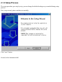
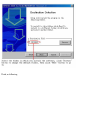
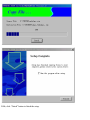
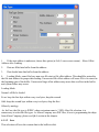
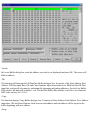
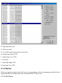
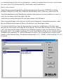
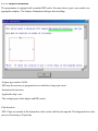
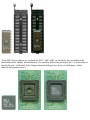
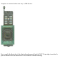
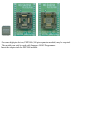
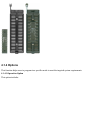
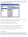
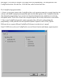
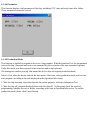
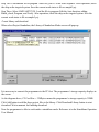
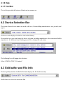
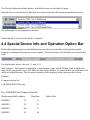
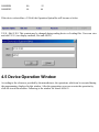
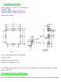
Distributed by:
www.Jameco.com ✦ 1-800-831-4242
The content and copyrights of the attached
material are the property of its owner.
Jameco Part Number 692457 Manual
Note: In order to connect the programmer easily and quickly, please connect the hardware after installing
the software.
Copyrights
Software
2003-2008 XELTEK
User’s Guide Copyright
2003-2008 XELTEK
Copyrights © 2003-2008 XELTEK
The distribution and sales of the product are intended for use by the original purchaser under the terms of
the License Agreement. This document may not, in whole or part, be copied, photocopied, reproduced,
translated or reduced to any electronic medium of machine-readable form without prior consent in
writing from XELTEK.
The information in this document is subject to change without notice.
SUPERPRO® is the trademark of XELTEK.
1. General Description
1.1 INTRODUCTION
1.1.1 What is Superpro?
The SUPERPRO is a series of cost-effective, reliable, and high-speed universal programmers. They are
designed to communicate through a USB or parallel port (model dependent) and to operate with most
IBM-compatible desktop computers and notebook computers. Their menu-driven software interface
makes them easy to operate.
Programming hardware includes the following items:
·A programming module (including a 40 or 48 pin ZIF)
·An AC adapter w/ dual range switching power supply (model dependent)
·A USB or parallel connecting cable
·Optional socket adapters to accommodate PLCC, TSOP, SOIC, SOP, QFP, TSSOP and BGA package
types are available.
·Software (CD)
Software includes the following features:
·Supports Windows 95/NT/2000/XP
·Programming support for a large number of devices (1500-11000) including PROMs,
PLDs and MCU from more than 100 manufacturers (model dependent).
E/EPROMs,
·Support formats in Binary, Intel (linear & segmented) Hex, Motorola S, Tektronix (linear & segmented),
Jed, POF etc.
·Device insertion test (48 pins or less) to detect defective chip, improper inserted device and loose
contacted pin (model dependent)
·Integrated full screen buffer editors with commands for fill, copy, move, swap, etc.
·Auto-generation of electronic serial numbers (model dependent)
·Project and selecting history
1.1.2 Manual Organization
This booklet consists of five main chapters:
Chapter 1: Provides an introduction to the SUPERPRO series, including system requirements.
Chapter 2: Provides system set up information, such as set-up of the hardware and software as well as
solutions for communication error if encountered.
Chapter 3: Provides pre-programming guidance and device selection, loading and reading data.
Chapter 4: Provides explanation for each software command and its functions.
Chapter 5: Provides guidance for trouble shooting and error messages.
1.1.3 Manual convention
The following conventions are used in this manual:
·The names of all keyboard keys are enclosed in angle brackets,
For example the Enter (or Return) key is shown as <Enter>
the Page Up key is shown as <PgUp>
·The cursor keys are shown as follows:
Left arrow key = <Left arrow>
Right arrow key = <Right arrow>
Up arrow key = <Up arrow>
Down arrow key = <Down arrow>
·Unless stated otherwise, keystrokes are not case-sensitive. e.g.: Both ‘A’ and ‘a’ are acceptable.
1.1.4 System Requirements
The minimum requirements are as follows:
·A Personal Computer, IBM or compatible, desktop or laptop, one USB port (USB 1.0) or one
parallel port (model dependent)
·Windows 98/NT/2000/XP operating system
·CD-ROM driver
·Hard disk of at least 20MB of spare capacity
1.1.5 Programmer Package
Standard package contains the following:
·A programmer module
·A parallel or USB connecting cable (model dependent)
·An AC adapter or a dual range switching power supply (model dependent)
·The installation software CD
·User’s Guide
·Registration card
2. System Setup
Parallel-based programmer’s software installation is straightforward and self-explanatory. If it’s your
first time to use the USB-based programmer of XELTEK, this chapter will help you to properly install
the software and connect the hardware. USB devices are PnP devices. At first installation, Windows will
start with “new hardware wizard” to scan all available INF files, and find out the appropriate driver. In
order to avoid unwanted complication during installation of USB device, we strongly suggest that you
install the software first. The setup program will handle the needed INF files and drivers automatically.
2.1 Software Setup
The content in 2.1.1, 2.1.2, 2.1.3, and 2.1.5 is applicable for both USB-based and Parallel-based
programmers.
2.1.1 Setup from CD-ROM
Insert the CD into a CD-ROM driver and the setup program will start automatically, if not, please run
SETUP.EXE in the root path.
Caution: Each model has its own software, please do not mismatch.
2.1.2 Download software from the Internet
You can download the specific software for a certain model at Xeltek website. It is usually a
self-extracting file. You only need to run this file to setup the software.
2.1.3 Setup Process
The setup procedure goes step by step, you can change the default settings as you needed during setup
process.
First, setup wizard, please read the text carefully.
Click “next” button
Second, select destination fold
Third, as following
Click “Install” button
Fourth, copying files please wait
Fifth, click “Finish” button to finish the setup.
2.1.4 Hardware Setup
Connect the programmer module to the computer’s USB port or parallel port. Turn on the programmer
power switch.
The driver installation is very simple, only need to wait until new hardware wizard finish installation
during the installation, please don’t run any other program.
2.1.5 Running the Program
The program for the programmer has a standard Windows UI, including pull down menus and buttons,
etc. User should master MS Windows OS know-how and use of pointing device such as a mouse or
trackball.
As the program started, it will communicate with the programmer immediately and begin initialization.
If communication error occurred,
Please check the steps below:
·Connect the programmer to PC, and turn on the power switch
·Correct installation. If the programmer is connected before the software installation, PC will detect new
hardware. The window appears as follows:
Please click “Cancel” to avoid troubles.
2.2 How to resolve the communication error
If incorrect installation makes the PC fail to communicate with the programmer, please follow the steps
below.
Windows 98/ME: reinstall the software, turn off the power switch of the programmer, wait a few
seconds, turn on the switch, wait until the drivers are installed, run the program again.
Windows 2000/XP: With the programmer’s power switch turning on, open the device management (in
‘Control Panel’, switch to classic View, open ‘System’,click ‘Hardware’ property), find the USB device
with “?”, right click it and select uninstall. Then reinstall the software, turn off the switch of programmer,
and turn on after a few seconds.
Caution: Under Windows XP, there are some options during the driver installation, please don’t change
the default settings.
3 Quick Guide
This chapter helps users understand the whole process of IC program. The content includes:
·The UI of the software
·The steps of device programming
3.1 Description of Interface
The interface is as following:
1. Main Menu
4. Edit Buffer
2. Toolbar
3. Select Device
5. Device Messages
7. Operation Toolbar
8. Device Function
9. Operation Message 10. Process Bar
6. File Message
3.2 The process of the programming
3.2.0 Hardware Preparation
First, make sure the programmer is properly connected with the PC, and communication established
successfully with the PC. (Some SMD devices need adapters, please contact Xeltek or its dealers for your
adapter needs.)
Second, insert the chip correctly. (Instruction for SMD and non-standard insertion will appear on the
screen when the selection of the device is made, if no instruction appears, chip insertion orientation
should follow the guideline of the chips marking near the pin-driver socket.)
3.2.1 Select the device
Click on “Select Device” button or click on “Device”, select the device for programming from the main
menu. The Select windows will popup. First select the Device Type (E/EPROM, BPROM, SRAM, PLD,
or MCU), followed by manufacturer and device part number from the screen. Click OK button or
double-click the device to confirm your selection. Typing in the device part number in the Search box
may also be used to search chips.
3.2.2 Load data into Buffer
Writing the data into memory buffer of the chip basically does chip programming. Therefore, to load the
data, you may load it from disk or copy master data by reading data from the master chip.
Loading a file
You may load a file into the memory buffer by clicking File menu in the main screen and select Load
File. In the Look In dialog box, select the folder and file name you wish to load. In the File Type box,
select the relevant data type. At this point, the selected data will be loaded into the memory buffer. Please
go to the Buffer edit screen and check if the data is loaded properly.
Note: Some Hex or S record files contain non-zero file start address. In this case, the start address should
be entered in the File address box.
Reading data from master chip:
Insert the master chip in the socket and make the selection of the device to read from. In the Function
screen, click on Read, which copies the data from the master chip into the memory buffer. At this point
you may go to the memory buffer edit screen and check if the data is loaded correctly. The data may be
saved to a disk for later use.
Note: some devices have no read function or are encrypted, under this condition data cannot be read
from.
3.2.3 Options
1) Operation Option, including:
·Insertion Test, check the pin contact before programming
·ID Check, check device’s ID before programming
·Beeper On, beeper sound off when the operation succeed or fail
· Auto Increment, when programming add a number label to the designated place so that each chip has a
different label
·change the start and end address of programming zone of the device
·Verify Mode, according to the requests, select specific VCC voltage verification in order to check the
programming chip correctly
2) Edit Auto, in the Function Screen, every device has a basic Auto operation, which automatically
execute the operation of device step by step. Normally select the following programming steps,
·Erase
·Blank-_check
·Program
·Verify
·Security or Protect
3) Dev. Config, as for the chip requires configuration, it must be properly configured before
programming to ensure the chip can be used on the targeted system
4) Dev. Information, some devices have special requests or conventions of programming, so user should
adjust operation steps or buffer data after carefully read the text in the Dev. Information box
5) Production Mode, in order to program chip in large number, with the help of insertion test, users do
not need to use keyboard and mouse repeatedly, only simply inserting and plucking out the chip under
the Production Mode.
3.2.5 Program the Data in Memory Buffer into a Chip
If the chip package is not DIP encapsulation, user may need to buy the adapter according to the info in
the Adapter box. (Contact Xeltek for selection and purchase the adapters.)
Insert the chip properly into the socket; following by these steps:
·Blank Check, this step can be skipped if the chip is brand new
·Program
·Verify, this step is necessary. The programming cannot be implemented unless passing the Verification
·If the chip to program is not blank, you should add Erase before the Blank Check.
·If encryption is required, add Security or Protect after Verify
·User can choose Auto to finish all operation by one step.
4 Description of Function
After reading the Quick Guide, you may want to know the specific process of programming. This chapter
will tell you all the function of the programmer.
·menu and tool bar
·select device and device info box
·edit buffer and file info box
·device function screen
·operation info screen
·status bar
4.1 menu and tool bar
4.1.1 File
4.1.1.1 Load
The two data types of device are Data (HEX/ASCII) and Fuse
For most EPROM and SCM, the data type is Data (HEX/ASCII), for PLD device is Fuse.
After device selection, the software will identify the data type automatically, to see the data type by
opening the buffer edit box
Files are loaded into one of two buffer types, HEX/ASCII buffer (EPROM, MCU etc.) and JEDEC
buffer (PLD/PAL).
·
For data type Data (HEX/ASCII), select Load menu, the Load File box popup.
To select a data file to be loaded, the path and the file name should be entered into the name field. If the
full path or the exact name of the file is unknown, then a partial path may be entered using wild cards,
e.g. ‘*.*’ or ‘*.bin’.
Based on the saving mode, the files are divided into various formats. You need to select the relevant data
types after selecting the file so that the data can be loaded correctly. The file types include Binary (or
POF), Intel HEX, Motorola S record and Tektronix Hex.
File Type box as following (no such box under JEDEC files)
1.
If the start address is unknown, choose this option (at Left, Lower screen corner) – Show Offset
Address after Loading.
2.
Data are filled into buffer from this address
3.
Data loaded into data buffer from this address
4.
Loading Mode, some files have non-zero file start or file offset address. This should be entered in
the file start address for proper data loading. Uncorrected file offset address will cause FFs to be stored in
the beginning part of the buffer. Uncorrected large offset address may cause data overflow in the buffer
and system failure may occur.
Loading Mode:
Normal: all file be loaded
Even: keep the first byte within every two bytes; drop the second
Odd: keep the second byte within every two bytes; drop the first
Others by analogy.
·As for Fuse, the file type is JEDEC whose extension name is *.JED. After file selection, it is
unnecessary to select the file types. As Altera Company uses POF files, if user is programming the chips
from Altera Company, please see Q&A section in the chapter.
4.1.1.2
Save
This selection will save the current data in the buffer to disk.
For E/EPROM, BPROM or MCU device types, Save File window will popup. Select the folder and
filename to be saved under. Next, File Type dialog box will popup for selecting file type to be saved
under.
For PLD devices, the Save JED File dialogue box will popup for entering the file name.
4.1.1.3 Recent Project
By saving the file path of recent project, it is convenient for user to reopen the projects.
4.1.1.4 Exit
This command closes the programmer software and returns you to the control of the operating system.
4.1.2 Buffer
The menu manages data in the buffer.
4.1.2.1 Edit
The selection brings up Fuse Buffer Edit window if the device buffer type is Fuse; otherwise, brings up
Data Buffer (HEX/ASCII) Edit window. You may edit the buffer data on the screen with the following
keys:
<PageUp> Page up
<PageDown> Page down
<Ctrl-PageUp> Move cursor to the beginning of the buffer
<Ctrl-PageDown> Move cursor to the end of the buffer
<Home> Move cursor to the beginning of the line
<End> Move cursor to the end of the line
4.1.2.1.1 HEX/ASCII data buffer
The HEX/ASCII data buffer is 8-bit wide. TAB key may be used to switch between HEX and ASCII
data for editing. According to the rule, if required to enter start and end addresses, the value of start
address must be less than that of the end address.
·Locate:
In Locate Buffer dialog box, enter the address you wish to see displayed and press OK. The cursor will
blink at address.
·Fill
The function will bring up the Fill Data Into Buffer dialogue box. It consists of the Start Address, End
Address, Fill Data input lines, OK and Cancel buttons. Input desired data to be filled into the Fill Data
input line, and specify the range by indicating the beginning and ending addresses. For the Fuse Buffer
Edit window, the data will be either 1 or 0. For the Data Buffer Edit window, it will be a two character
HEX code, such as AA, 55, E4
·Copy
The function displays Copy Buffer dialogue box. It consists of Start Address, End Address, New Address
input lines, OK and Cancel buttons. Data between start address and end address will be copied to the
buffer beginning with new address.
·Swap
Swap MSB and LSB byte order for the specified word width in the address range.
For example, assuming data buffer addresses 0-10(HEX) is:
12 34 56 78 90 AA BB CC – DD EE FF 11 22 33 44 55
The word width for selecting is:
16 Bits (2 bytes), after swapping the data is:
34 12 78 56 AA 90 CC BB – EE DD 11 FF 33 22 55 44
32 Bits (4 bytes), after swapping the data is:
78 56 34 12 CC BB AA 90 – 11 FF EE DD 55 44 33 22
64 Bits (8 bytes), after swapping the data is:
CC BB AA 90 78 56 34 12 – 55 44 33 22 11 FF EE DD
·Radix
Toggles between HEX and DEC memory address display.
·Search
Searches for a combination of HEX/ASCII codes
·Next
Performs the next search for the search string in Search
4.1.2.1.2 Fuse Buffer
The data for editing is either 0 or 1, which has two explanations according to the different devices.
·1 represents an intact fuse
0 represents a blown fuse
·1 represents an blown fuse
0 represent an intact fuse
User can define the significations of 0 or 1 according to the devices’ manual and JEDEC files.
Note the three important options in the Buffer Edit dialogue box:
·Buffer clear at IC change: clear the buffer after device being selected
·Buffer clear on data load: clear the buffer before load file data
·Buffer save when exit: save buffer data when exit. When entering the system again, load the saved data
automatically.
4.1.2.2 Save Buffer
User can save the data in the text file format to the specified file, the way is as following:
HEX/ASCII data buffer
00000000 4D 5A 90 00 03 00 00 00-04 00 00 00 FF FF 00 00 MZ.._..._.......
00000010 B8 00 00 00 00 00 00 00-40 00 00 00 00 00 00 00 ........@.......
00000020 00 00 00 00 00 00 00 00-00 00 00 00 00 00 00 00 ................
00000030 00 00 00 00 00 00 00 00-00 00 00 00 80 00 00 00 ................
Fuse data buffer
00000768 10011010101010101010101010101010
00000800 01101010101010101010101010101010
00000832 10100110101010101010101010101010
00000864 10101010011010101010101010101010
00000896 10101010101001101010101010101010
00000928 10101010101010100110101010101010
00000960 10101010101010101010011010101010
00000992 10101010101010101010101001101010
4.1.2.3 Encryption Table
The Load Encryption Table, with its two sub-menus, manages an encryption array. The two sub-menus
will appear only if the chip selected is equipped with an encryption array.
Load: Brings up the Load Encryption Table dialogue box. Enter the name of the file to be loaded in the
input line provided.
Edit: Opens the Encryption Buffer Edit window for viewing and editing.
4.1.2.4 E-Fuse
If the data type of the device is Fuse and the JEDEC file has E field, bring up the E Field Fuse Data Edit
dialogue box. Please refer to the chapter of Fuse Buffer.
4.1.2.5 Vector Table
This opens the Vector Buffer Edit window. If a test vector table is included in the JEDEC file, the
software will load the test vector table to the buffer when the JEDEC file is loaded. Each line display one
vector table, each bit represents one pin’s test character, from left to right related to the first to the last
pin. Following is the test vector of a 14-pin device.
Z: High impedance state
X: Don’t care state
N: Vcc and Ground (output pins are not tested)
H: Output logic High (VOH)
L: Output logic Low (VOL)
C: Clock pin
1: Input logic High (VIH)
0: Input logic Low (VIL)
4.1.3 Device
Before any operation, please select the device for programming, so that the programmer could select the
proper algorithm according to the name and manufacturer of the devices.
4.1.3.1 Select Device
The function brings up Select Device dialogue box. It consists of Manufacturer list viewer, Device Name
list viewer, Device Type button and OK, Cancel button, and Search Edit box.
How to select a device?
·Select the device type through the Type Selection button, total five groups: E/EPROM (including
EPROM, EEPROM, FLASH), PLD, B/PROM, DRAM/SRAM, MCU. If not sure, please select All.
·Select the manufacture in the Manufacturer column, at this point user can check whether it’s correct or
not by the icon shown at the lower right of the box.
·Select the device name through the Device Name column, click OK button.
Since some printed name on the chips may include speed, temperature, encapsulation parameter, when
they are different with the names in Device Selection box, user should ignore them.
Use of the Search Edit box: Since the large quantity of the devices and difference of the chips’ name
there may be some trouble in selecting the device directly. The Search Edit box helps to select. Entering
a few vital characters the number of the devices will decrease greatly so that it is convenient for select
the specific device. For example, as entering ‘89’ in the Search Edit box all the devices, whether its name
or manufacturer containing ‘89’ will be listed in the list viewers. The search function is sensitive to the
sequence of the character string. The character strings such as ‘819’, ‘DA8S9’ will be listed, but ‘98’ will
be ignored.
Using Search Edit box reduces the number of devices listed, a convenient function for users; but please
be sure only correct character string is entered, or users would not be able to find the specific devices.
Therefore please double check the character string or make the Search Edit box blank.
Except the device types, user also need to select the encapsulation of the device. For example, as the
picture above, DSB9C420 represents a DIP chip, DS89C420@PLCC44 represents a PLCC 44-pin chip,
DSB9C420@TQFP44 represent a TQFP 44-pin chip.
4.1.3.2 Dev. Information
Since the manufacturers’ requests and the conventions of the special devices, some devices have special
requests in operation except the basic steps, which includes:
·arrangement of the data buffer content
·explanations of the devices’ special operation
In the popup Special Information dialogue box, user should read the info carefully, and configure
properly according to the requests to ensure programming successfully. These special information
contain in the device’s manual.
4.1.3.3 Adapter Information
The programmer is equipped with a standard DIP socket. For some device types, users need to use
appropriate adapters. The Adapter Information dialogue box including:
·Adapter type such as SA244
·PEP may be necessary to program devices which have larger pin count.
·Instruction for insertion
·Applicable chip’s size
·The wiring layout of the adapter and DIP socket
Chip Insertion
·DIP: Chips are inserted at the bottom line of the socket with the nick upward. The diagram below is the
process of inserting a 28-pin chip.
·None-DIP: Socket adapters are available for PLCC, QFP, SOIC etc. Insert the chip according to the
instructions in the Adapter Information box. The insertion follows the position of pin 1. It is necessary to
identify the pin 1 of the chip. In the Adapter Insertion dialogue box, there is a solid square, which
indicates the position of pin 1.
·Adapters are inserted in the same way as DIP devices.
Note: usually the front side of the chip is placed upwards; but for PLCC 20-pin chip, it needs to be
placed with the front side downwards. This method is called Dead Bug.
·For some high pin devices, PEP3000 (100 pin expansion module) may be required.
The module can only be used with Superpro 3000U Programmer.
Insert the adapter into the PEP3000 module.
·For economic programmer, perhaps special insertion needed.
4.1.4 Options
This function helps users to program in a specific mode to meet the targeted system requirements.
4.1.4.1 Operation Option
This option includes:
·Insertion Test
Only for chips with 48 pins or less (include the chips with more than 48 pins which are transformed to 48
pins or less by a adapter)
As select this option, the programmer will check the pin contact status before programming, including
check for loose contact, device insertion orientation error, etc.
The cases include:
·No device connected
·Non-connection or poor pin contact
In the case of the diagram above, for example, pin 32 has trouble. The resolution is:
Check the pin contact first. If the contact is nothing wrong, please replace the chip with another to ensure
whether the former chip is broken or not. The pin number is referred to DIP chip’s pin number. If an
adapter is used, it is referred to the adapter’s pin number. For example, an 84-pin chip is transformed to
48-pin by an adapter and inserted to the socket. The pin number is referred to the 48-pin chip’s pin
number. The reference is in the Adapter Information dialogue box. For example, PLCC44/D44, PLCC44
refers to PLCC44-pin chip, D44refers to DIP 44-pin chip. The device may have no 44-pin DIP
packaging, but this doesn’t affect the programming.
·Device inserted backwards or damaged
Please take out the chip and insert again properly. If the problem still exists, the chip may be damaged or
non-functional.
Device is inserted improperly. Please refer to Device Insertion.
·An unmatched device inserted
If Insertion Test finds errors, users can click Abort to stop the programming, or click Retry to run
Insertion Test again, or click Ignore to program despite the errors.
·ID Check
Device ID is the code read from the chip to identify the manufacturer and the device type. In the
Operation Option box, this option is activated after selecting the device. This means the device ID will be
checked before programming. If the device ID is unmatched, an error window will popup.
Click Yes to ignore the error and continue programming.
Click No to abort the programming.
When the ID is unmatched, the software will auto search for matched devices and display in the error
window for reference.
·Beeper On
During the operation the beeper in the programmer will sound off to indicate the result of operation, such
as Insertion Test error, ID unmatched, programming successfully or failed etc. This option allows user to
turn on or off the beeper.
·Auto Increment
In the Operation Option box, select both AutoInc. Option and AutoInc.Format.
Auto Increment allows users to add related info (8 bytes default) into the device. After each successful
programming, the software auto changes the value by the specified increment mode.
Note: no auto Increment under the standalone mode.
AutoInc. Set
·Set Start Address
·Set End Address
·Set increment value with any number less than 10
The address here is referred to the buffer address. Start address must be larger than the end address.
Auto Increment: define overflow value, from start address; unit is byte (max Dec 255).
When does the increment cease and carry to next address?
While a value reaches the overflow, carrying to next address (+1), this address becomes the start value.
Binary: start value is 0; overflow value is 256
ASCII Decimal: start value is 30 (Hex 0); overflow value 39+1 (Hex more than 9)
ASCII Hex: start value is 30 (Hex 0), overflow value is 46+1 (Hex more than F) 9+1=A
User defines: BCD is default. Start value is 00 (Hex). Overflow value is 09+1 (Hex). If user defines, a
config file and source program (in the CD) is required. In the VC++ environment revise and create the
file ‘UserAuto.dll’, and use it to replace the same name file in the Bin directory.
For example, there are 64 chips. Their IDs are from 0001 to 0064, which are in the end address of 89C51
EPROM. User selects the mode of 4 bytes and Dec. The steps are listed as below:
Click Option> Auto Increment
Set Start to FFC and End to FFF
Set IncValue to 1
Set Format to ASCII Decimal
Go into Buffer Edit screen at ASCII zone. Change buffer as follows:
FFC: 30 FFD: 30 FFE: 30 FFF: 31
During the programming, Operation Info screen displays:
Current AutoIncrement Data=0001
The last 4 bytes of buffer data is:
FFC: 30 FFD: 30 FFE: 30 FFF: 31
If programming succeeds Operation Info screen displays:
Current AutoIncrement Data = 0002
The last 4 bytes of buffer data is:
FFC: 30 FFD: 30 FFE: 30 FFF: 32
Device
This selection allows users to program only utilize part of the chip, applicable to most E/EPROM (Flash)
device.
For example, MACRONIX MX29F200B TSOP48 is a 16 bit Flash device. Its program zone start and
end address is 0 and 1FFFF (Hex), and data buffer capacity is (1FFFF+1)*2=40000 (Hex,). Since it’s a
16-bit device, data buffer capacity is 2 times of that of the device. The default method is programming
from the start address to the end address. If user only wants to program the chip’s last part, please set the
start address to 10000 (Hex), and remain the end address default value. Thus the data for programming
are the data in data buffer between 20000 (Hex) and 40000 (Hex).
This function not only makes programming more flexible but also saves time under the Production
Mode.
Verify Mode
It is necessary to verify after the programming of a chip. According to the reference to the manufacture,
the requests of VCC voltage for verification are different.
1. Use VCC (+/- 5%) or (+/- 10%) to verify. For example, VCC=5.00V. Use VCC=5.00V to verify once,
or use VCC=4.74V and VCC =5.25V to verify twice (+/- 5%), or use VCC=4.50V and VCC=5.50V to
verify twice (+/- 10%).
2. Use MinVcc and MaxVcc to verify.
Note: The Operation Option will vary with the various devices. i.e. Most SCMs don’t allow user to set
the start and end address of the device.
4.1.4.2 Edit Auto
In the Edit Auto dialogue box, all devices have an Auto option, which is like a batch command. This
function allows the software auto operate in order displayed in the right column. For example, select
ATMEL AT89C51, open Edit Auto dialogue box. On the left of the box is Device Functions column in
which all device operations are displayed. On the right of the box is Auto column in which operations
needed and operation sequence are displayed.
In the diagram above, the operation sequence is Erase, Blank_check, Program, Verify, Lock_Bit124.
Add button: add the functions in the left column to the right Auto column
Delete button: remove the functions from the Auto column
Delete All button: remove all the functions from the Auto column
Double click on the functions listed in the left column to add them to the Auto sequence.
Double click on the functions listed in the Auto sequence to remove them.
Once the Auto menu has been edited, the auto sequence will be saved in the hard disk.
This option helps to improve the efficiency of programming.
4.1.4.3 Device Config
Some SCMs allow users to configure special mode, such as memory block mapping, watchdog timer,
clock and encryption. In the diagram is the ConfigWord of DALLAS DS89C420, which has watchdog
and three encryption modes. Some SCMs have some ConfigWord that its option may be divided into 2 or
more pages. Users need to configure every page before the programming. The configuration of the
ConfigWord includes 8-bit edit line, 16-bit edit line, radio box and check box.
The ConfigWord program includes
1. If there is encryption option in the ConfigWord, the verify operation cannot be executed; therefore the
software will disable encryption automatically and write the other options in the ConfigWord into the
chip during the programming. Users need to use Operation Option Security and Protect to write the
encryption option. If you select None in the encryption option, the Security and Protect is unavailable.
2. Since some ConfigWord cannot be written separately, they will not be written during the
programming. At this point the relevant Operation Option is required, such as Write_Option.
Different devices require different ConfigWord. Reference is in the devices’ manual.
Some FLASH devices also use ConfigWord to execute Protect function and display segment protect.
4.1.4.4 Parameter
This function displays vital parameter of the chip, including VCC, time and retry times after failure.
These parameters cannot be revised.
4.1.4.5 Production Mode
This function is applied to program a device in a large number. With the Insertion Test, the programmer
detects the chip’s insertion and carries out automatically the execution of the auto operation sequence.
Under this mode, user does not need to move mouse and to tap keyboard.
If a nonsupport window pops up, that means the device does not support production mode.
Advice: First select the device and edit the auto menu. After tests, select production mode, and execute
auto program, according to the info displayed in the Operation Info screen.
1. Wait for chip insertion: insert the chip into the socket properly, reference in Insertion Test
2. Wait for chip off: program finished; please take the chip off. At this point, check the result of
programming, whether success or failure, according to the info in Operation Info screen. To end the
production mode, please click Cancel button.
4.1.5 Project
Project file includes:
·current device’s info, such as manufacturer name, type, pin info, ConfigWord, current buffer data and
data file name. (Since the buffer data can be revised, the buffer data may differ from the data file)
·all Operation Option settings
Auto program sequence
Project records all the preparation works before programming. Users can return to the previous
environment by opening the project. In this way, users can avoid error during the work,
Note: The software update and reinstallation to another folder will make the project saved previously
become unavailable.
4.1.5.1 Load Project
Load project by selecting the file in the File dialogue box. According to the file, change device, buffer
data and operation option etc.
4.1.5.2 Save Project
Save the current work environment to specified project.
4.1.5.3 Standalone
Some types of SUPERPRO are equipped with keypad, LCD and Disk to save data. The programmer of
these types can work under a standalone mode, which is applicable for volume-production. The entire
algorithm file, user data file, operation and device options should be configured in this menu followed by
downloading these configurations and files to the programmer. Thus the programmer is able to work
under standalone mode. The downloaded library, which is stored in the programmer’s storage block,
contains all the info for programming mainly the project file.
How to create a library?
·Create project file
Under the standalone mode, the programmer can program the same devices with different methods, or
program different devices. The max number of methods the programmer supports is dependent on the
capacity of the storage block. The methods are dependent on the project file saved.
For example, two Atmel AT89C51 chips, they are going to be programmed with different files. If the
capacity is enough, add an AMD AM27C128. The steps are as following:
Step One: select Atmel AT89C51, and load the file to program. Edit Auto function, adding Erase,
Blank_check, Program, and Verify. After operation, check the chip on the targeted system. Save the
current work status to file as sample1.prj
Step Two: Load another file to program. Add Lock_Bit123 to the Auto sequence. After operation, check
the chip on the targeted system. Save the current work status to file as sample2.prj.
Step Three: Select AMD AM27C128. Load the file to program. Edit the Auto function, adding
Blank_check, Program, and Verify. After operation, check the chip on the targeted system. Save the
current work status to file as sample3.prj.
·Create library and download
When select Project Standalone, the Library of Standalone Mode screen will pops up.
It is necessary to connect the programmer to the PC first. The programmer’s storage capacity displays in
the screen.
As the diagram above, CF Card Size = 32Mbytes means the programmer’s storage capacity is 32MB.
Click Add button to add the three project files to the library. Click Download Library button to start
download. Wait a moment for finishing download.
Now the programmer is able to work under a standalone mode. Reference is in the Standalone Operation
User Manual.
4.1.6 Help
4.1.7 Tool Bar
The tool bar provides the buttons of functions in common use.
4.2 Device Selection Bar
The recent selected device names are saved in the bar. (Also including manufacturers, size, pin info, and
types)
The devices info displayed in this bar also include history.
By using this bar, users can change the device selection, including manufacturer, device name and buffer
capacity, etc. It’s different from Loading project file to change the work status.
The following box will popup after selection.
Select ATMEL AT89C51 Continue?
4.3 Edit buffer and File Info
This bar quickly launches the Buffer Edit and displays the file loaded recently.
Buffer button is referred to sub-menu Edit
The file info displayed includes history, which allows user to select the file again.
Since the device selected may be different, the event of data lost, file format unmatched may occur.
The following box will popup after selection.
Reload the file E:\test.bin in the buffer. Continue?
4.4 Special Device Info and Operation Option Bar
Before the programming, users should obtain the special device info and set the operation option
properly according to the targeted system’s request. The toolbar below will facilitate user to finish this
work.
For detailed info, please refer to 4.1.3 and 4.1.4
Data Compare: This function is applicable to most memory chips and SCM chips. Data in buffer and
chip will be compared by bytes. The different data and the address it is stored will be recorded and saved
in file in the Bin directory. The file name and path will be displayed in the Operation Info screen.
Example:
Compare result in file
c:\SP3000U\BIN\27256.cmp
Tile: SUPERPRO Data Compare Result file.
Displacement Buffer address
Chip Data
000000E0
2F
11
000002E1
30
22
000005E2
0D
33
000008E3
4C
44
Buffer Data
00000BE4
0A
55
00000DE5
44
66
If the device selected has a U-Field, the Operation Option Bar will become as below
U.E.S.: Edit U.E.S. This content may be changed during reading device or Loading files. Users can view
and edit U.E.S. (two display methods, Hex and ASCII)
4.5 Device Operation Window
According to the references provided by the manufacturer, the operations, which can be executed during
the programming, displayed in this window. After the preparation, users can execute the operation by
click the icon in the window. Following is the window for Atmel At89c51.
The function displayed may differ from chip to chip. The frequently-used operations are explained
below.
Auto: The function executes series of operation in sequence. Please refer to 4.1.4.2
Program: The function writes the data from the buffer into the chip. The Verify function is performed in
two modes. One mode is verifying while programming. This method ensures the correctness of
programming. If an error occurs, the error message will be displayed and the process will be ceased. The
other method is not verifying during the programming. Even if an error occurs, the process will not be
ceased. When the last address is written, the program successful message will be displayed. Anyway, the
program successful message only means that the program process is finished, the correctness is
dependent on the result of verification.
Read: The function reads the content of the chip into the buffer. To view the content read, please open
the Buffer Edit dialogue box.
Note:
1) For the encrypted chips, their content cannot be read
2) For the chips with ConfigWord, the ConfigWord will be read and save to ConfigWord buffer.
3) For PLD devices, their test vector isn’t in the chip, unable to read
Verify: The function compares the content of the buffer to that of the chip. If there is any discrepancy,
verification will cease and failure message will be displayed. For most memory chips and SCM chips, the
failure message includes address and data. For PLD chip, the message displayed is dependent on the
programming reference. Only the chips that pass verification can be recognized as chips being
programmed correctly.
Blank check:
This function checks if the device is in blank state, which is dependent on the data manual. If selecting
fill data buffer blank as devices changed, the programmer will fill all the HEX/ASCII buffer data with FF
or 00 (Hex), and Fuse buffer data with 1 or 0 after the devices selected. An encrypted chip is displayed as
a blank chip. EEPROM doesn't need Bank_check.
How to write over a chip into blank?
1) For the chip that can be erased electrically, execute Erase
2) For the chip that can be erased with ultraviolet ray, use the ultraviolet ray eraser for 3-30 minutes.
3) For OTP, once written it is unable to be written over back to blank again.
Erase:
Erase the chip to blank state. This operation can only be executed with the chip that can be erased
electrically. EEPROM doesn't need to execute this operation. If you need a chip of blank state you can
directly program the blank data to the chip. Some chips that can be erased electrically are able to become
an OTP by configure the ConfigWord. Please refer to the device data manual.
Protect:
1)
Encrypt the data to make them unreadable. Whether the protect state is readable or not, affect the
editing of the operation function. When the protect state is unreadable, the Protect operation will be
added to the operation function window. As long as the Protect function is executed, the chip will be
protected. If the protect state is readable, the state None and all the protect options will be listed out for
user to select. The protect operation will be executed according to the ConfigWord. If user select None,
the protect operation is non-functional.
Note: Some manufacturers’ chips with window will be used again after full-protect, and ultraviolet ray
eraser is also unable to erase.
2)
For FLASH chips, this function is for protecting the data in the chips. The protected chip is not
re-writable before the protection removed. The Erase operation would remove the protection.
This operation is required to be used with Dev. Config. Users need to identify the Sector to protect.
There are two ways to select the Sector,
1.
Users enter the address of several (max 8) sectors to decide the sectors to protect. After the protect
operation, the sectors whose addresses are entered will be protected.
2.
Divide the chip into several sector groups, users can only choose these groups to protect.
Security: equal to Protect,
Erease_All: equal to Erase
Protect_All: equal to Protect
Lock_Bit: the notion for protects. Please refer to the manual.
Above are commonly used functions. For some devices, which have special requirements and functions,
the operation function window may be different.
For detailed information, user could refer to:
1. The manual of the device
2. Dev. Information
3. The technical support of XELTEK
4.6 Operation Info Window
This is for the interaction between the software and users. The operation process, result and history will
be displayed in this window.
Above is the example.
ATMEL AT89C51: device selection correct. If error occurs, please refer to error info revise
Erasing…..
Erase OK!: Erase successfully
Blank_check……
Blank_check OK!
Program…..
Program OK!
Verifying……
Verifying OK!
Lock_Bit 1&2&3….: protecting.
The functions of Lock_Bit123 is as following:
1)
MOVC instructions executed
2)
Verify is disabled
3)
External execution is disabled
Executing one function will finish several operations. User should select the function according to the
manual in order to avoid operation in errors.
Lock_Bit 1&2&3 OK!
0:00’09’’23 elapsed: executing Auto takes 9.23seconds
Programmer not found: the red letters mean that errors occurred.
There is a special status in the Operation Info window. It records the times of success and failure. The
judgment is: Program OK! means a success; otherwise, a failure.
Reset button will set both the success and failure to 0.
4.7 Status Bar
This bar displays the menu info, the process of operation, and a Cancel button.
Click Cancel button, the box will pop up
Cancel process. Continue?
The Cancel operation may destroy the chip, please use it selectively.
5 Trouble Shooting
During the operation, user is able to monitor and correct the progress of the operation through Operation
Info window and message window. This chapter will help user to deal with some common trouble.
5.1 Data file Format
Detail usage of the file type dialogue box.
5.1.1 Intel Hex, Motorola and Tektronix formats
The data for program usually are stored in the data file. Commonly used formats are Intel Hex, Motorola
and Tektronix.
These file formats save data in text mode, which include data info and address info. The offset address is
not always zero. If user loads the file directly, some errors may occur such as the location of data in
buffer incorrect or unable to load file. The message window is as following:
Invalid file type, or all file data overflow
Resolution:
1)
Confirm the file type and ensure the buffer able to load all the file
2)
Find the file’s offset address. User can do this by selecting the option to show the starting address
of the file. Thus the starting address of file will be displayed after file selection. For example:
File Offset Address (min): 0x0000E0000 (Hex)
This means the offset address of the file is not 0; users need to move the data of the address to the
address 0. To do that, user should reload the file and enter E000 in the file start address edit line in the
File Type dialogue box.
5.1.2 Program a split File to Two or More Chips
By the File Load Mode in the File Type dialogue box, users can program a file data to several chips of
the same type. The how-to is as following:
1.
Based on byte (8bit), divide the file into two parts by the odd and even address, and program the
two parts into two chips respectively. User selects odd in the File Load Mode, the data in the address
0,2,4,6…. will be programmed to one chip; user selects even, the data in the address 1.3.5.7…. will be
programmed to the other chip.
2.
Based on byte (8bit), take a byte within every four bytes, and program the file to four chips. User
selects one byte within every four bytes in the File Load Mode box, the data in address 0,4,8,12…. will
be programmed to one chip, others by analogy.
3.
Based on byte (16bit), take the former two bytes (or the latter two) within every four bytes to form
a 16bit byte, and program to two chips.
5.1.3 Program Two or More Files to One Chip
Explain this by using an example of programming three files to a chip. The requests is as following:
From the address 200 (Hex) of file sample1 program the data to the address 0 of the chip; from the
address 0 (Hex) of file sample2 program the data to the address 3000 (Hex) of the chip; from the address
4000 (Hex) of file sample3 program the data to the address 4000 (Hex) of the chip.
Step one:
Open Buffer Edit dialogue box, with Clear Buffer During File Loading unselected.
Step two
Select file sample1. Enter 0 in the buffer start address line and 200 in the file start address line. Load the
file.
Select file sample2. Enter 3000 in the buffer start address line and 0 in the file start address line. Load the
file.
Select file sample3. Enter 4000 in the buffer start address line and 4000 in the file start address line. Load
the file.
Step three
Program
Users can also save the data in buffer to a file sample4, then directly load sample4 to program
5.1.4 File of POF Format
Some companies, such as ALTERA, save data in POF format. During file loading, a File Type box will
pop up for user to select.
1)
POF file, which is created by compiler, will be transformed to Fuse data and be checked when
loaded to buffer.
Unmatched file to this chip: this means this POF file is not for this chip, please replace it with a matched
one.
The POF file has errors:
Load POF file dll error (not found): the secondary file has errors; please contact technical support.
2)
Other formats. Mainly the JED file. The data will save in a JED file after reading the chip. Use this
mode when loading the file next time.
5.2 Adapter Selection
The programmer is equipped with a ZIF socket and is designed to accept DIP devices with 48 pins (40
pins for Superpro Z) or less. Adapters are required to accept non-DIP devices or devices with more than
48 pins. There are two types of adapter, universal and specific. Universal adapters are applicable for all
devices of same packaging and leads. Specific adapters are applicable for certain devices only.
Why are specific adapters required?
Technology in IC packaging is evolving and new package types have been introduced over time,
therefore adapters are needed in order to accommodate the devices come in different package types or
with more pins or leads.
For the devices with pins between 48 and 100, if using a universal adapter, users need an expander to
expand from the 48 pin driver to 100 pin driver; while for common devices the specific adapter is able to
transform the device to a 48-pin directly. At this point, user has two options, one is using a universal
adapter, and the other is using a specific adapter. The thing to pay attention to is be careful when
determining the device names during selecting. For example, if using universal adapter, the user should
select 87C196KC@PLCC68 (universal adapter), otherwise select 87C196KC@PCC68 (special adapter).
For 100pin or more devices, the specific adapter is required.
How to select the correct types of adapter?
After device selection, if the device required an adapter, the Adapter dialogue box will pop up. It
includes the type of the adapter and the size of applicable chip. For example,
Adapter type is SA244
Above is the information of PLCC package,
E=pitch=1.27mm
Width=D(16.6mm)/E(17.5mm)
Length= D(16.6mm)/E(17.5mm)
For selecting specific adapters, it requires more detail checking. For example, following is a specific
adapter for PLCC68
The specific adapter consists of two parts: top board (with transform socket, type is SA648) and bottom
board (type is B6805).
Users should buy the adapter according to the information provided.
Note: Since there is wiring diagram in the Adapter Info dialogue box, users can make the adapter by
themselves. But it is strongly suggested to purchase the adapter from XELTEK due to the potential
reliability issues of self-made adapters.
5.3 Other Messages
Please edit Auto first: the Auto consequence is blank; please edit Auto.
Enter a string to search for: the search dialogue is blank; please enter a string or ASCII code to search
for.
The string for search is blank. Input it in Search dialogue: use search function in Buffer Edit dialogue
box. First search, continue, Search Next.
Search pattern not found !: no string or ASCII matched.
User chip is MfgID = 0089, DeviID = 0051: the chip ID detected is different from the specified ID of the
manual.
ID check error. Ignore: ignore the ID error and continue operation
ID check error: ID error occurs, operation ceased
User can ignore the ID error and continue the operation; however, the consequence is that damage of the
chip may occur!
Pin check error. Ignore: error occurs during pin check. Ignore it and continue
Pin check error: error occurs during pin check and operation ceased
Programmer not found: the programmer is not connected to the PC or connected improperly.
Programmer not ready: shut down the power switch and open again after a few seconds
Programmer is running: please wait until the operation finished
File open error: open file failed
Out of Memory: memory overflow
Production mode isn’t available for this chip: Since the production mode is dependent on the pin check,
the chips without pin check function are not applicable for production mode.
Cancel production mode
Too long file name
User cancel: user cancels the operation
Can’t cancel!: cancel failed
Not a project file: the file selected is not a project file. After update the software may not be able to
identify the file created previously. At this point the user need to create the file again.
5.4 How to simplify the operation and improve
efficiency?
Advice is below:
Use Auto function
Use production mode
Use project file
Use standalone mode if possible
5.5 Why programming failed?
Please check the following steps:
Whether improperly select the type of device or not, including package, adapter, etc.
Whether select the adapter of original factory and insert the chip properly?
Whether update the software? The chip’s manufacturing process is always improving. Therefore the
configuration of the programmer is always changing. Please update the software regularly or contact us.
Whether the socket is smudgy or beyond its life cycle? Smudgy socket causes loose contact. The life
cycle of the socket is about thousand of times used; please replace the socket with a new one.
Whether the chip is protected, or write-protected? Please erase the chip or de-protect.
Whether the AUTO INC function is selected? If it is selected, the verify command can only be executed
in AUTO. Executing Verify separately after Program will fail when verifying the address storing count
value.
If your cases are not included above, please contact us to check if it is a hardware error.
Appendices
License Agreement
The copyright of the program and User’s Guide remain the property of XELTEK.
You may:
Copy the program for back-up purposes ONLY in support of its use on a single computer.
Transfer the program and license to another party if the other party agrees to accept the terms and
conditions of this agreement.
You may not
Use this product in a computer system or network, which allows the program to be operated by more
than one user at a time.
Modify, copy, or transfer the User’s Guide, other documentation or any copy.
Reverse engineering, de-compiling, or disassemble any program module or security device.
Limited Warranty
XELTEK warrants that its products will be free from defects in workmanship and materials, and shall
conform to specifications current at the time of shipment, for a period of one year from the date of
shipment. During the one-year period, any detective software or hardware products will be repaired or
replaced, at seller’s discretion, on a return to factory basis.
This warranty applies only to products properly installed and operated within specified environmental
conditions.
XELTEK’s responsibility under this warranty does not apply to:
Any product that has been repaired, worked upon, or altered by any person not duly authorized in writing
by XELTEK.
Any product that has been subject to misuse, negligence, accident, or its serial number has been altered.
Any program error caused by physically damaged CD.
The extended and joint liability of damages caused by hardware faults or software bugs.
Customer Support
SUPERPRO software is user friendly for your usage and requires minimal technical support. The
program comes with a comprehensive User’s Guide. If you cannot find the answer in the manual, you
can turn to your dealer or distributor or XELTEK. XELTEK provides telephone (number available at
website) technical assistance during normal business hours from 9:00am to 5:00pm. Please have your
invoice number ready when calling, as we cannot answer your questions without it. Software updates are
available free from the web site.
Pre-call Check List:
If you are having difficulty understanding the program, have you studied the User’s Guide?
If there seems to be a problem with the software, can you reproduce it?
If the program has displayed an error message, please write down the message.
When phoning or faxing or e-mailing for technical assistance, have your invoice number ready.
Are you using the newest version of the software?