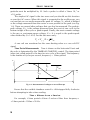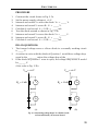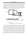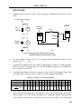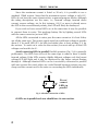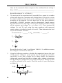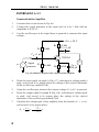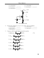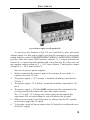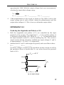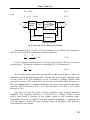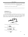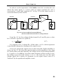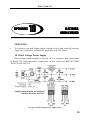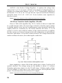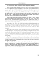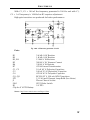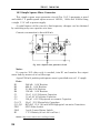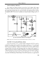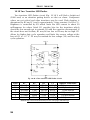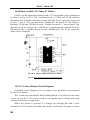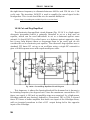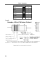
1
Khalil Ismailov ELECTRONICS LABORATORY MANUAL Qafqaz University Press Baku, 2011 ELECTRONICS LABORATORY MANUAL Prepared by Kh.A. Ismailov, Professor Department of Computer Engineering, Qafqaz University Reviewed by A.Z. Melikov, Professor Associate Member of the National Academy of Sciences of Azerbaijan Republic, The Institute of Cybernetics of the National Academy of Sciences of Azerbaijan Republic Reviewed by A.Z. Adamov, PhD Department of Computer Engineering, Qafqaz University Design Sahib Kazimov Is printed as a publication of Qafqaz University by the proposal of the Publishing Committee dated from 06.12.2010 (minute No 7) and decision of the Senate dated from 15.12.2010 (minute No Ç-QU-15000-000.100) Book is printed by “Sharg-Garb” Publishing House. Tel: (+994 12) 374 83 43, 374 75 62 Copyright Qafqaz University, 2011 Copyright Khalil Ismailov, 2011 Qafqaz University Press No: 45 Baku, 2011 CONTENTS PREFACE SAFETY Introduction Current Hazards and Voltage Safety Precautions Neat Working Area In Case of Electrical Shock INSTRUCTIONS FOR ELECTRONICS LABORATORY Organization Purpose and Procedure Grading Equipment Handling General Tips 5 6 6 6 7 7 8 8 8 9 10 10 EXPERIMENT 1. Oscilloscope and Function Generator Operation EXPERIMENT 2. Diode Characteristics EXPERIMENT 3. Half-Wave and Full-Wave Rectification EXPERIMENT 4. Zener Diodes EXPERIMENT 5. Light-Emitting Diodes EXPERIMENT 6. Bipolar-Junction Transistor EXPERIMENT 7. Junction Field-Effect Transistor EXPERIMENT 8. Op-Amp Characteristics EXPERIMENT 9. Linear Op-Amp Circuits EXPERIMENT 10. Electronic Hobby Circuits 11 29 38 55 69 78 94 109 120 133 REFERENCES 168 APPENDIX A Important electrical units, abbreviations and symbols APPENDIX B Using the Metric System to Help Some Familiar Metrics APPENDIX C Resistor Color Coding APPENDIX D Capacitor Color Coding APPENDIX E General Purpose NPN and PNP Transistors APPENDIX F JFET Transistors APPENDIX G Useful Electronics Sites 169 170 171 173 174 177 179 PREFACE The experiments in this laboratory course are designed to cover the theoretical and analytical materials in “Electronics”. Each experiment begins with a set of stated objectives, text references, and required equipment, followed by a procedure for meeting each objective. The objective of the experiments is to enhance the students’ understanding of important analytical principles developed in this course by engaging them in the real-world application of these principles in the laboratory. In addition to further develop the students’ laboratory practice for experimentally testing and evaluating electrical circuits. Preparing the lab is very important as it will save time and allows working more efficiently. The pre-lab includes reading the lab assignment in advance, and doing the pre-lab assignment specific to each lab experiment. All pre-lab assignments have to be handed in with the main lab report at the beginning of the class. The manual is designed as an individualized learning package and involves the student in the activities of learning. Many illustrations and line drawings are used to familiarize the student with circuit recognition and analysis, since, this is an important part of being a good electronics technician. Each unit follows the same format so that the person using the book can become accustomed to the learning procedure. The basic experiments are given on how to test the device and verify its theory of operation. Fill-in questions are given at the end of each experiment to emphasize the important points gained from performing the experiment. This manual contains several appendixes at the end. The students is encouraged to become familiar with the contents of the appendixes early. Appendix A covers descriptions of important electrical units, abbreviations and symbols. Using the Metric System to Help Some Familiar Metrics is provided in Appendix B. The information about resistor and capacitor color coding is provided in Appendices C and D. Appendices E and F covers product descriptions and pin configuration of general purpose NPN/PNP transistors and N-/P-channel FET transistors. A list of useful electronics sites is provided in Appendix G. 5 Khalil Ismailov SAFETY Introduction The experiments in this manual do not use a voltage greater than 30V (or ±15V); therefore, the chance of getting an electrical shock is greatly reduced. However, all voltages do have the potential to burn materials and start fires, to destroy electronic components, and present hazards to the person performing the operations. Common sense and an awareness of electrical circuits is important whenever you are working on these experiments. Before actual work is performed, sufficient instruction should be acquired in the proper use and safety requirements of all electronic devices. Current Hazards and Voltage Safety Precautions It takes a very small amount of current to pass through the human body from an electrical shock to injure a person severely or fatally. The 50-Hz current values affecting the human body are as follows: Current value 1 mA (0.001 A) 10 mA (0.01 A) 100 mA (0.1 A) Over 100 mA Effects Tingling or mild sensation. A shock of sufficient intensity to cause involuntary control of muscles, so that a person cannot let go of an electrical conductor. A shock of this type lasting for 1 second is sufficient to cause a crippling effect or even death. An extremely severe shock that may cause ventricular fibrillation, where a change in the rhythm of the heartbeat causes death almost instantaneously. The resistance of the human body varies from about 500,000 Ω when dry to about 300 Ω when wet (including the effects of perspiration). In this case, voltages as low as 30 V can cause sufficient current to be fatal (I=voltage / wet resistance=30 V/300 Ω=100 mA). Even though the actual voltage of a circuit being worked on is low enough not to present a very hazardous situation, the equipment being used to power and test the circuit (i.e., power supply, signal generator, meters, oscilloscopes) is usually operated on 220 V AC. To minimize the chance of getting shocked, a person should use only one hand while making voltage measurements, keeping the other hand at the side of the body, in the lap, or behind the body. Do not defeat the safety feature (fuse, circuit breaker, interlock switch) of any electrical device by shorting across it or by using a higher amperage rating than that specified by the manufacturer. These safety devices are intended to protect both the user and the equipment. 6 Elecrtronics Neat Working Area A neat working area requires a careful and deliberate approach when setting it up. Test equipment and tools should be set out on the workbench in a neat and orderly manner. Connecting wires from the test equipment to the circuit under test should be placed so as not to interfere with testing procedures. Before power is applied to a circuit, the area around the circuit should be cleared of extra wires, components, hand tools, and debris (cut wire and insulation). In Case of Electrical Shock When a person comes in contact with an electrical circuit of sufficient voltage to cause shock, certain steps should be taken as outlined in the following procedure: 1. Quickly remove the victim from the source of electricity by means of a switch, circuit breaker, pulling the cord, or cutting the wires with a wellinsulated tool. 2. It may be faster to separate the victim from the electrical circuit by using a dry stick, rope, leather belt, coat, blanket, or any other nonconducting material. CAUTION: Do not touch the victim or the electrical circuit unless the power is off. 3. Call for assistance, since other persons may be more knowledgeable in treating the victim or can call for professional medical help while first aid is being given. 4. Check the victim’s breathing and heartbeat. 5. If breathing has stopped but the victim's pulse is detectable, give mouthto-mouth resuscitation until medical help arrives. 6. If the heartbeat has stopped, use cardiopulmonary resuscitation, but only if you are trained in the proper technique. 7. If both breathing and heartbeat have stopped, alternate between mouthto-mouth resuscitation and cardiopulmonary resuscitation (but only if you are trained). 8. Use blankets or coats to keep the victim warm and raise the legs slightly above head level to help prevent shock. 9. If the victim has burns, cover your mouth and nostrils with gauze or a clean handkerchief to avoid breathing germs on the victim and then wrap the burned areas of the victim firmly with sterile gauze or a clean cloth. 10. In any case, do not just stand there – do something within your ability to give the victim some first aid. 7 Khalil Ismailov INSTRUCTIONS FOR ELECTRONICS LABORATORY Organization The laboratory work is a group activity. Students will be divided into groups of two or three. All members of a group are expected to be present and participate in conducting an experiment with as much equal contribution as possible. All members of a group are expected to come prepared, and complete the work within the scheduled laboratory period with their laboratory partners. No individual member and no individual group will be allowed to do an experiment outside the scheduled times except under extenuating circumstances and only with the consent of the instructor. Purpose and Procedure The purpose of this course is to cultivate in the student a degree of independence in carrying out an engineering task. The burden (and reward) of success is the student's, not the instructor’s. The student will perform specific electronic experiments as indicated by handouts for each experiment. These handouts are generally specific but leave much room for independent approaches. In the lectures background and motivating material and a certain degree of guidance for the experiments will be given; but the exact experimental set-up or diagrams will not be given. This is the responsibility of the student. The instructor (or the teaching assistant of the laboratory session) may give a moderate degree of specific guidance, mainly by asking the student pertinent questions to direct the student onto a correct path. He will do this only after the student has demonstrated substantial serious effort to solve the problem. The student should not expect to receive from the lab instructor exact circuit diagrams. The instructor will, however, point out errors in diagrams or hook-ups as far as this can reasonably be done. The grade given to the student for the experiment will partly depend on the degree of independence of the student. If everything else fails, the instructor will provide a good diagram, but this will be done at a severe penalty in the grading. Contrary to popular belief, most of the work must be done by the student before he or she comes to the laboratory. One should study the problems using common sense and any required textbooks and/or reference books. One must prepare a complete procedure for the experimental work including alternatives and must know what components and equipment are needed and allow for substitution if the first choice is not available. One must study the 8 Elecrtronics problem before coming to the laboratory so that the general trend of results is anticipated. This will make it possible to recognize "nonsense" results and correct the experimental procedure. Unnoticed wrong results will be considered worse than incomplete results in the grading, since the theory and the laboratory is available to the student to validate results. Each student must have a laboratory manual. The manual will contain the preliminary work done as well as the complete work plan for the experiment. It will also contain every test and check made, all in-lab computations, modifications of circuit or procedure, and results. The instructor may examine the work done and grade the preliminary during the lab periods. A concise, but complete, neatly prepared final report for each experiment by each member of the group must be handed in to the instructor within one week after the completion of the experiment. It is expected that the circuits, design calculations and data to be the same for two reports written by the members of the same group. But, this cannot be used to justify near identical reports to be submitted. Particularly, discussions, comments, conclusions and the overall style should reflect individual contribution and originality. A good presentation is clear, concise, and informative. It makes good use of graphics, has good writing style and presents ideas in a nice logical sequence. Some longer experiments will be allowed to be completed in two weeks. A quiz may be given at the beginning of each experiment. The instructor will give some overall guidance at the beginning. The work plans will be checked in the laboratory and graded. In summary the student’s endeavors will include: 1. Preparation of work plans for each experiment based on independent reading and analysis, and lecture suggestions. 2. Preparation for and taking of lab quizzes. (Note that preparation of a good work plan will aid in quiz preparation. 3. Conducting of the actual experiments in the laboratory. 4. Preparation of a final report for each experiment. Grading Grades will be assigned over the following categories with the indicated weights (approximately): Lab reports: 25% Preliminary work/design 50% Experiment and participation 25% Discussions/Conclusions NO LAB EXPERIMENT OR ITS REPORT MAY BE SKIPPED. LATE REPORTS LOSE 50% PER WEEK, COMPOUNDED. 9 Khalil Ismailov Equipment Handling Never take for granted that the equipment or components are in good condition. Always check all equipment before you start the experiment. Make certain the power supply has ripple free output voltage and that the oscilloscope has the correct gain in the ranges of interest. Check all diodes and transistors with an ohm-meter. Make sure resistors and potentiometers are close to the indicated value. Make sure that capacitors are not shorted, nor opened. In case of equipment failure, keep the malfunctioning equipment on your bench; do not swap equipment from other benches. Equipment sets are assigned to groups. Do not attempt to repair malfunctioning equipment. Do not even replace fuses. Call the lab instructor/technician for appropriate action. General Tips When something doesn’t work as you expect, be skeptical about all facets of your design, fabrication and test of the circuit. Although test equipment may fail from time to time, problems are almost always due to errors in design, documentation or wiring; faulty components occasionally; or a misunderstanding of how to use the test equipment. In the laboratory the experimenter interacts with natural phenomena which tend to be brutally honest and unforgiving in evaluating a poorly thought out experiment. Group interactions can be difficult; but Engineering is inherently a discipline requiring much team effort. Thus, the skills developed in working effectively in a grouped environment are quite important. It is the responsibility of each student to create an effective group where everyone contributes substantially. 10 Elecrtronics EXPERIMENT 1 OSCILLOSCOPE and FUNCTION GENERATOR OPERATION OBJECTIVES 1. 2. 3. 4. To understand the operation and use of an oscilloscope To learn to measure DC and AC voltages with the oscilloscope To use an oscilloscope to observe repetitive time varying waveforms To use a function generator to create repetitive waveforms BASIC INFORMATION The Oscilloscope The oscilloscope or “scope” as it is better known is one of the most versatile pieces of laboratory test equipment (Fig. 1.1). It is really a type of analog voltmeter with an arbitrary zero. It can read DC voltages as an offset voltage and as well as AC voltages by displaying the true wave form. Most modern oscilloscopes are capable of measuring AC signals over a wide range of frequencies. The heart of the oscilloscope is the cathode ray tube, which generates the electron beam, accelerates the beam to a high velocity, deflects the beam to create the image, and contains the phosphor screen where the electron beam eventually becomes visible. The electrons are called cathode rays because they are emitted by the cathode and this gives the oscilloscope its full name of cathode ray oscilloscope (CRO) or cathode ray tube (CRT) oscilloscope (Fig. 1.2). The electron beam emitted by the heated cathode at the rear end of the tube is accelerated and focused by one or more anodes, and strikes the front of the tube, producing a bright spot on the phosphorescent screen. 11 Khalil Ismailov Fig. 1.1. Cathode Ray Oscilloscope The heart of the oscilloscope is the cathode ray tube, which generates the electron beam, accelerates the beam to a high velocity, deflects the beam to create the image, and contains the phosphor screen where the electron beam eventually becomes visible. The electrons are called cathode rays because they are emitted by the cathode and this gives the oscilloscope its full name of cathode ray oscilloscope (CRO) or cathode ray tube (CRT) oscilloscope (Fig. 1.2). The electron beam emitted by the heated cathode at the rear end of the tube is accelerated and focused by one or more anodes, and strikes the front of the tube, producing a bright spot on the phosphorescent screen. The electron beam is bent, or deflected, by voltages applied to two sets of plates fixed in the tube. The horizontal deflection plates, or X-plates produce side to side movement. As you can see, they are linked to a system block called the time base. This produces a sawtooth waveform. During the rising phase of the sawtooth, the spot is driven at a uniform rate from left to right across the front of the screen. During the falling phase, the electron beam returns rapidly from right or left, but the spot is “blanked out” so that nothing appears on the screen. Although the oscilloscope can eventually be used to display practically any parameter, the input to the oscilloscope is voltage. In this way, the time base generates the X-axis of the V/t graph. The general laboratory oscilloscope can accept as low as a few millivolts per centimeter of deflection up to hundred of volts using the built-in attenuator and external probes. 12 Elecrtronics TIME/DIV X-POS Time base waveform Spot move across screen Y 0 t Spot Spot blanked out during flyback Trigger Time base Heater CH1 SIGNAL INPUT AC/DC switch Cathode Anodes Y-amplifier Signal waveform Y-plates X-plates Cathode ray tube Y 0 Electron beem t VOLTS/DIV SCREEN Y-POS Fig. 1.2. Cathode Ray Oscilloscope block-diagram The slope of the rising phase varies with the frequency of the sawtooth and can be adjusted, using the TIME/DIV control, to change the scale of the Xaxis. Dividing the oscilloscope screen into squares allows the horizontal scale to be expressed in seconds, milliseconds or microseconds per division (s/DIV, ms/DIV, µs/DIV). Alternatively, if the squares are 1 cm apart, the scale may be given as s/cm, ms/cm or µs/cm. The vertical input also will have a switch for AC or DC input signals. When the AC/DC switch is in the DC position, the probe is connected directly to the Y-amplifier. When the switch is in the AC position, there is a coupling capacitor between the probe and the amplifiers. The reason to allow the measurement of low-level AC signals which may be on the same wire as a high-level DC voltage. If the probe is connected directly to the amplifiers, the scope trace moves on the scale an amount equal to the voltage applied. If this voltage is a high voltage, say 100 V the vertical attenuator must be set to an insensitive position in order for the trace not to be deflected beyond the viewable portion of the screen. With the vertical sensitivity thus set, a small AC signal on the same wire could not be measured, when the vertical input switch is in the AC position, a capacitor blocks the direct current from reaching the amplifiers. With the direct current blocked, the vertical sensitivity can be set so the AC signal can be easily seen and measured. The Y-amplifier is linked in turn to a pair of Y-plates so that it provides the Y-axis of the V/t graph. The overall gain of the Y-amplifier can be adjusted, 13 Khalil Ismailov using the VOLTS/DIV control, so that the resulting display is neither too small nor too large, but fits the screen and can be seen clearly. The vertical scale is usually given in V/DIV or mV/DIV. The trigger circuit is used to delay the time base waveform so that the same section of the input signal is displayed on the screen each time the spot moves across. The effect of this is to give a stable picture on the oscilloscope screen, making it easier to measure and interpret the signal. Changing the scales of the X-axis and Y-axis allows many different signals to be displayed. Sometimes, it is also useful to be able to change the positions of the axes. This is possible using the X-POS and Y-POS controls. For example, with no signal applied, the normal trace is a straight line across the centre of the screen. Adjusting Y-POS allows the zero level on the Y-axis to be changed, moving the whole trace up or down on the screen to give an effective display of signals like pulse waveforms which do not alternate between positive and negative values. A dual trace oscilloscope can display two traces on the screen, allowing you to easily compare the input and output of an amplifier for example. The dual trace oscilloscope provides for amplification and display of two signals at the same time, thereby permitting direct comparison of the signals on the CRT screen (measure the phase displacement of two waveforms, and so on). Front Panel Controls Front panel controls permit you to control the operation of the oscilloscope. They may be grouped functionally as: Main Oscilloscope Controls According to Function Display Intensity Focus Beam Finder Vertical Coupling (AC-Ground-DC) Volts/Div Y-position Channel Select Magnification Cal (Calibrated) Horizontal Time base (Sec/Div) X-position Magnification Cal (Calibrated) Triggering Coupling Source Level Slope Mode The above function set is summarized for a typical oscilloscope only. The oscilloscope in the laboratory that you will be using may have more functions. For detail operation of the oscilloscope, you should refer to the user’s manual of the oscilloscope. 14 Elecrtronics Connecting the oscilloscope to the circuit under test The input impedance of an oscilloscope is rather high, being on the order of 1 MΩ, which is desirable for measuring voltages in high impedance circuits. The attenuator sets the sensitivity of the oscilloscope in the common 1-2-5 sequence. As an example, the input attenuator could provide for 10, 20, 50, 100, 200 mV, etc., per centimeter. The input attenuator must provide the correct 1-2-5 sequence attenuation while maintaining a constant input impedance, as well as maintaining both the input impedance and attenuation over the frequency range for which the oscilloscope was designed. The oscilloscope is connected to the circuit under test by means of a probe (or set of probes) as illustrated in Fig. 1.3. The probe includes a measurement tip and a ground clip and connects to the oscilloscope by a BNC connector via a flexible, shielded cable which is grounded at the oscilloscope. This ground serves as the reference point with respect to which all signals are measured. The shield helps guard electrical noise pick up. Voltage Measurements A screen is divided into centimeter divisions in the vertical and horizontal directions. The vertical sensitivity is provided (or set) in volts/cm, while the horizontal sensitivity is provided (or set) in time (s/cm). The magnitude of the signal can be determined from the following equation: Signal voltage Vs = voltage sensitivity (V/cm) × deflection (cm) If a particular signal occupies 6 vertical centimeters and the vertical sensitivity is 5 mV/cm, signal voltage Vs = (5 mV/cm) (6 cm) = 30 mV. Fig. 1.3. Connection of the oscilloscope to the circuit under test Sometimes an attenuator probe is used to expand the range of the scope. This probe has a high-value resistor in it which acts as a voltage divider with the scope input resistance. As a result, whatever voltage is read on the scope 15 Khalil Ismailov graticule must be multiplied by 10. Such a probe is called a “times 10,” or ×10, probe. The simplest AC signal is the sine wave and you should use this function as your first AC source. When this signal is connected to the oscilloscope, you can see that you can easily measure the peak AC voltage, Vp, which is defined as the voltage measured from the center or zero position to the peak (see Fig. 1.4). There are several other voltages that can also be measured. The peak-topeak voltage, Vp-p, is the voltage measured from the crest of one cycle to the bottom trough of the cycle or peak-to-peak. Finally, the most common voltage is the rms or root-mean-square voltage, Vrms. It is equal to the peak-to-peak value divided by (2×1.414). For the sine wave only: Vp = Vp − p / 2 = 2Vrms A one volt rms waveform has the same heating value as a one volt DC signal. Time Period Measurements Time is shown on the horizontal X-axis and the scale is determined by the TIMEBASE (TIME/DIV) control. The time period (often just called period) is the time for one cycle of the signal. The frequency is the number of cycles per second, frequency = 1/time period. v Vp Vrms 0 t Vp-p T Fig. 1.4. Measurement of voltages on an oscilloscope Ensure that the variable timebase control is click-stopped fully clockwise before attempting to take a time reading. Time = distance in cm × time/cm For example, if time period=4.0cm×5 ms/cm=20ms then frequency= =1/time period=1/20ms=50 Hz. 16 Elecrtronics Functional descriptions of an oscilloscope OS-5020: Coupling (AC-GND-DC): Permits selection of coupling of the input channel. When set to DC, the entire signal (AC plus any DC components) is displayed. When set to AC, DC signals are blocked by a capacitor and only AC is displayed. When set to ground, the input channel is isolated from the input source and is grounded internally. VOLTS/DIV: This is the scope’s vertical sensitivity control. It is a calibrated control that establishes how many volts each major vertical scale division represents. For example, when it is set for 1 V/DIV, each grid line represents 1 volt. Each channel has its own independent VOLTS/DIV control. CAL.: This is the fine adjust control, usually located in the inner of the VOLTS/DIV knob. When this knob is turned to the fully clockwise direction, it is at the calibrated location (the normal position of this knob) for the outer knob setting, i.e., the vertical scale of the scope is defined by the VOLTS/DIV knob. When the CAL. knob is turned away from the calibrated position, the waveform displayed in the scope will start to be attenuated. Vertical POSITION: This is the vertical position control. Each channel has its own control. It moves the trace up or down for easier observation. It is not calibrated. Channel Select: Permits displaying CH1, CH2, both channels, their sum or difference. Timebase (V MODE): This is a calibrated control that selects how many seconds each major horizontal division represents. It is calibrated in s, ms, and µs. One control handles all channels. There is also CAL. knob for the time base. The CAL. knob is located at the inner of the TIME/DIV knob. Its operation is similar to that of the previous one for the VOLTS/DIV. Magnification: For both CAL. knobs of the VOLTS/DIV and TIME/DIV, the CAL. Knob also acts as the magnification switch. The magnification is ×5 or ×10 with the knob pulled out. Horizontal POSITION: Positions the trace horizontally. One control handles all channels. Trigger Source: Selects the trigger source, e.g., CH1, CH2, an external trigger, or the AC power line. Trigger Level: Permits you to adjust the point on the trigger source waveform where you like the triggering to start. 17 Khalil Ismailov Trigger Slope: Selects whether the scope is to trigger on the positive or negative slope of the trigger source waveform. Trigger Mode: Modes include AUTO – the sweep always occurs, even with no trigger present, NORMAL – a trigger must be present, and SINGLE SWEEP – a trigger is required but only one sweep results. INTENSITY: Adjusts the intensity of the displayed beam. FOCUS: Adjusts the sharpness of the displayed beam. AUTO: Some oscilloscopes with electronic control are fitted with a button which automatically selects an appropriate timebase, triggering mode and horizontal gain. Function Generator The function generator is a supply that typically provides a sinusoidal, square-wave, and triangular waveforms for a range of frequencies and amplitudes. Although the frequency of the function generator can be set by the dial position and appropriate multiplier, the oscilloscope can be used to precisely set the output frequency. The scope can also be used to set the amplitude of the function generator since most function generators simply have an amplitude control with no level indicators. The model FG-8002 (Fig. 1.5) is an advanced function generator which provides functions of function generator, pulse generator and sweep oscillator including following versatile features: - 18 Wide frequency range from 0.02 Hz to 2 MHz. Versatile waveforms are selectable in sine wave, square wave. Triangle wave and pulse wave, etc. TTL level square wave output is available for signal source for digital circuit experiments. Variable symmetry to generate sawtooth and pulse waveform Frequency of output signal can be controlled by applying voltage from 0 to +10 V to VCF IN connector. The linear sweep function provides SWEEP FUNCTION CONTROL from 1:1 to 100:1. DC voltage from 0 to +10 V can be overload upon output waveform Maximum attenuation over 40 dB. Elecrtronics Fig. 1.5 Function Generator SUMMARY The most common scope in use today is the triggered-sweep scope. Older scopes were the recurrent sweep type. 2. The typical scope has four sections: vertical; horizontal; trigger, or sync; and display. 3. The vertical section of the scope conditions the input and causes the beam in the CRT to be deflected vertically. 4. The horizontal section of the scope controls the horizontal sweep of the CRT electron beam. It causes the beam to sweep at an accurate rate, so frequency can be calculated from the sweep time. 5. The trigger section of the scope controls how the beam is synchronized with the incoming signal to cause the waveform to be stable. 6. The display section of the scope controls brightness, focus, etc. 7. The scope has controls to allow adjustment of vertical sensitivity, vertical and horizontal beam position, etc. 8. The AC-DC switch allows the display of either AC or DC signals. 9. The function generator typically provides a sinusoidal, square-wave, and triangular waveform for a range of frequencies and amplitudes. 10. Advanced function generator provides functions of function generator, pulse generator and sweep oscillator. 1. 19 Khalil Ismailov SELF-TEST Check your understanding of the introductory information by answering the following questions. 1. What is the purpose of the horizontal time-base section? 2. Why is the AC-DC switch setting important when you are making lowlevel AC measurements? 3. The term attenuate means what? 4. What are the four sections of the scope? 5. What kind of waveforms is provided by the function generator? 6. What are the functions of the advanced function generators? MATERIALS REQUIRED • • • Oscilloscope (OS-5020) Variable DC power supply (GP-4303TP) Function generator (FG-8002) PROCEDURE Setting up an oscilloscope Before placing the instrument in use, set up and check the instrument as follows: 1. 20 Set the following controls as indicated. POWER Switch INTEN Control FOCUS Control AC/GND/DC Switch VOLTS/DIV Switch ×5MAG Switch Vertical POSITION Controls INV Switch VARIABLE Controls V MODE Switch TIME/DIV Switch VARIABLE Control Horizontal POSITION Control ×10MAG Switch OFF (released) Mid rotation Mid rotation DC 10 mV ×1 Mid rotation Norm Fully CCW CH1 1 ms CAL Mid rotation ×1 Elecrtronics Trigger MODE Switch Trigger SOURCE Switch Trigger LEVEL Control SLOPE Switch AUTO VERT Mid rotation Button out 2. Press the POWER Switch. The POWER lamp should light immediately. About 30 seconds later, rotate the INTEN. Control clockwise until the trace appears on the CRT screen. Adjust brightness to your liking. 3. Turn the FOCUS Control for a sharp trace. 4. Turn the CH1 Vertical POSITION Control to move the CH1 trace to the center horizontal graticule line. 5. See if the trace is precisely parallel with the graticule line. 6. Turn the Horizontal POSITION Control to align the left edge of the trace with the left most graticule line. 7. Set one of the supplied probes (Fig. 1.6) for ×10 attenuation. Then, connect its BNC end to the CH1 or X IN Connector. Fig. 1.6. Probe Scope probes are available with ×1 attenuation (direct connection) and ×10 attenuation. The ×10 attenuator probes increase the effective input impedance of the probe/scope combination to 10 megohms shunted by a few picofarads, the reduction in input capacitance is the most important reason for using attenuator probes at high frequencies, where capacitance is the major factor in loading down a circuit and distorting the signal. When ×10 attenuator probes are used, the scale factor (VOLTS/DIV switch setting) must be multiplied by ten. 21 Khalil Ismailov Single-trace Operation The OS-5020 is set up for single-trace operation as follows: 1. Set the following controls as indicated below. Note that the trigger source selected (CH1 or CH2 SOURCE) must match the single channel selected. (CH1 or CH2 V-MODE) POWER switch ON (pushed in) AC/GND/DC switches AC Vertical POSITION controls Mid rotation VARIABLE controls Fully CW V MODE switch CH1 (CH2) VARIABLE control CAL Trigger MODE switch AUTO Trigger SOURCE switch VERT Trigger LEVEL control Mid rotation 2. 3. 4. 5. Use the corresponding Vertical POSITION control or to set the trace near mid screen. Connect the signal to be observed to the corresponding IN connector and adjust the corresponding VOLTS/DIV switch or so the displayed signal is totally on screen. CAUTION> Do not apply a signal greater than 400 V (DC + peak AC) Set the TIME/DIV switch so the desired number of signal cycles are displayed. Adjust the Trigger LEVEL control if necessary for a stable display. If the signal you wish to observe is either DC or low enough in frequency, the AC coupling will attenuate or distort the signal. So, flip the AC/GND/DC switch or to DC. Dual-trace Operation Dual trace operation is the major operating mode of the OS-5020. The setup for dual trace operation is identical to that of single trace operation with the following exceptions: 1. Set the V MODE switch to either DUAL. Select ALT for relatively high frequency signals (TIME/DIV switch set to 0.5 ms or faster). Select CHOP for relatively low frequency signals (TIME/DIV switch set to 1 ms or slower). 2. If both channels are displayed in signals of the same frequency, set the Trigger SOURCE switch to the channel having the steepest-slope waveform. If the signals are different but harmonically related, trigger from the channel carrying the lowest frequency. Also, remember that if you disconnect the channel serving as the trigger source, the entire display will free run. 22 Elecrtronics Setting up a Function Generator 1. 2. 3. 4. 5. 6. 7. 8. 9. Pressing POWER Switch turns on power. POWER Lamp light up when power is on. Connect BNC end of the clip probe to the OUTPUT 50 Ω BNC socket. The lead is connected with a push and twist action, to disconnect you need to twist and pull. Push on of three knobs of FUNCTION Selector to get a desired waveform out of sine wave, triangle wave and square wave. Amplitude of output signal can be controlled by AMPLITUDE/PULL–20 dB knob. Maximum attenuation is more than 20 dB when the knob is rotated fully counterclockwise. Pulling this knob makes attenuation of 20 dB, so the output signal can be attenuated by 40 dB when this is pulled and rotated fully counterclockwise. Frequency range (Seven ranges: 1 – 0.02 Hz to 2 Hz, 10 – 2 Hz to 20 Hz, 100 – 20 Hz to 200 Hz, 1k – 200 Hz to 2 kHz, 10k – 2 kHz to 20 kHz, 100k – 20 kHz to 200 kHz, 1M – 200 kHz to 2 MHz,) is selected by FREQUENCY RANGE Selector. Output frequency within the selected range is varied by the Frequency Dial potentiometer. Sweep width is controlled by SWEEP WIDTH/PULL ON Control. Pulling the knob selects internal sweep and rotating it controls sweep width. Rotate it counterclockwise to get a minimum sweep width (1:1) and rotate it clockwise to get a maximum sweep width (100:1). To get a maximum sweep width, set the frequency dial to minimum scale (below 0.2 scale). Sweep rate (sweep frequency) of internal sweep oscillator is controlled by SWEEP RATE Control. Symmetry (duty cycle) of output signal waveform within range of 10:1 to 1:10 is controlled by SYMMETRY Control. The DC OFFSET control knob may be used to offset the waveform above or below ground (0 volts) by a DC voltage in the range ±10 volts. To adjust the DC level pull out the OFFSET control knob then turn slowly CW (positive volts) or CCW (negative volts). If the OFFSET knob is pushed in, there is no DC level, but only AC voltage exists in the output signal. Measurements 1. 2. Plug the power cable of the oscilloscope into the socket outlet in the bench. Practice setting up the scope to get a trace on the screen. Move the trace around. Work with all the controls until you understand their functions. 23 Khalil Ismailov 3. 4. 5. 6. Rotate the focus and intensity controls to get a sharply focused trace at a comfortable viewing level. Connect a probe to CH1 and set the channel selector to CH1 and use a ×1 probe. Set the TRIGGER to AUTO. Flip the AC-GND-DC coupling switch to GND (ground) and center the trace. Connect the output of the variable DC power supply to the input of the oscilloscope as shown in Fig. 1.7. Trace +V CH1 Variable DC power supply –V Ground clip Probe Fig. 1.7. Measuring DC voltage 7. 8. 9. Set the vertical attenuator to measure 0.5 V/cm. Make sure the vertical attenuator vernier (fine-adjust) control is in the CAL. position. The AC-DC switch should be set to DC. Measure the voltage of a 1-, 1.5-, and 2-V source (obtained from the variable power supply). Connect the probe as in Fig. 1.7 and set VIOLTS/DIV to 1 V. Set the output of the variable DC power supply to 2 V and note the beam deflection on the screen. From the deflection, compute the measured voltage. Fill in the table after doing step 9. Change VOLTS/DIV to 2 V, set the output of the variable DC power supply to 5 V and note the position of the trace. Make similar adjustments and fill in the following table. Input Voltage 2V 5V 15 V 10 V 15 V 22.5 V 24 Probe Volts/Div Setting ×1 ×1 ×1 ×10 ×10 ×10 1V 2V 5V Deflection Oscilloscope Voltage Value Elecrtronics 10. Replace the variable DC power supply with a function generator as shown in Fig. 1.8. Connect the CH 1 input of the oscilloscope to 50 Ω output of the function generator using a BNC-BNC lead (Fig. 1.9). Set input coupling on the oscilloscope to ground and center the trace. Change the input coupling to AC. Trace Oscilloscope Output Function Generator Ground CH1 Ground clip Probe Fig. 1.8. Measuring AC voltage 11. Set the function generator to 100 Hz. Now adjust it to display one, then two, and then four cycles of signal. What were your horizontal time-base settings? ___________________ . Use the trigger controls to cause the waveforms to move and then to be stationary (synchronized). 12. Set signal generator to any frequency. Set the vertical attenuator to 0.5 V/cm. Be sure the vertical attenuator vernier control is in the CAL. position. Measure the voltage of a 1-, 1.5-, and 2-V peak-to-peak (p-p) signal. 13. Connect the function generator to one of the inputs of the oscilloscope. Set the vertical attenuator to 10 V/cm and AC-DC switch to DC position. Switch the function generator on and pull out its DC OFFSET control knob then turn slowly CW (positive volts) or CCW (negative volts). What do you observe? ___________________________________________ _______________________________________________________________. 25 Khalil Ismailov OSCILLOSCOPE INPUT BNC Socket BNC plug CH1 FUNCTION GENERATOR 50 Ω OUTPUT Push and rotate Push and rotate Fig. 1.9. BNC-BNC lead 14. Flip the AC-DC switch to AC. What happens?_________________________________________________ ______________________________________________________________. 15. Set the function generator to a 2 kHz sine wave. On the oscilloscope, set the VOLTS/DIV switch to 1 V, the Trigger to positive slope, and the time base to 0.1 ms/Div. 16. Adjust the output voltage of the generator until you get a nicely sized sine wave on the screen. Record the waveform in Fig. 1.10. Set the Trigger to negative slope and record the waveform in Fig. 1.11. The peak to peak voltage is: ________ V. 17. Set the frequency of the generator to 500 Hz and change the time base to get 2 cycles on the screen (actually a bit more than two). Record the waveform and the time base setting in Fig. 1.12. 18. Set the waveform of the generator to square wave and complete Figs. 1.13 and 1.14. 26 Elecrtronics Volts/Div = Time base = Volts/Div = Fig. 1.10. Positive trigger Volts/Div = Time base = Fig. 1.11. Negative trigger Time base = Fig. 1.12. Waveform recording Volts/Div = Time base = Fig. 1.13. Positive trigger Volts/Div = Time base = Fig. 1.14. Negative trigger 27 Khalil Ismailov QUESTIONS 1. 2. 3. Is the time-base setting important when you are measuring direct current? Explain. How the magnitude of the signal is determined when you take measurements of voltage from the screen? If the vertical sensitivity is increased, it takes more signal to deflect the beam (true/false). Answers to Self-Test 1. 2. 3. 4. 5. 6. 28 To make the beam sweep across the CRT at a regular, predictable rate. This, in turn, allows for accurate frequency measurements. If there is any direct current on the same line with the low-level alternating current and the scope is set in the DC position, the trace may be detected off the screen. To keep the trace on the screen, the vertical attenuator must be set so insensitively as to make the low-level alternating current immeasurable. To make smaller. Vertical, horizontal, sync, and display. Sinusoidal, square-wave, and triangular waveforms for a range of frequencies and amplitudes. Function generator, pulse generator and sweep oscillator. EXPERIMENT EXPERIMENT 2 DIODE CHARACTERISTICS EXPERIMENT 2.1 TESTING SEMICONDUCTOR DIODES OBJECTIVE • To demonstrate a practical method of testing diodes with an ohmmeter. This is called a go/no go test. When p- and n-type silicon are joined as shown in Fig. 2.1, a junction diode is created. This two element device has a unique characteristic: the ability to pass current readily in only one direction. p n Fig. 2.1. Junction diode Connection of a negative battery terminal to the n-type and the positive battery terminal to the p-type silicon results in correct low and is called forward bias. Electrons and holes are repelled toward the p-n junction, where they recombine to form neutral charges and are replaced by free electrons (negative charges) from the battery. This movement of charges maintains a high forward current through the diode in the form of free electrons passing from the n material through the junction and the p material, toward the positive terminal of the battery. Because current flows in this connection, the diode is said to have a low forward resistance. The reverse-bias connection is shown in Fig. 2.2. The positive terminal of the battery attracts free electrons in the n-type silicon away from the p-n junction. The negative terminal of the battery attracts the holes in the p-type 29 Khalil Ismailov away from the p-n junction. Hence there are no combinations of free electrons and holes. Thus the majority current carriers in the diode do not support current flow. In this reverse-bias configuration, there is a minute current in the diode. This current is due to the minority carriers, that is, the holes in the ntype and free electrons in the p-type. For the minority carriers, battery polarity is correct to support current flow. Only a few microamperes of current flow as a result of the minority carriers. This is shown by the dotted arrows in Fig. 2.2. The reverse-bias connection results in a high reverse resistance in the diode. p n e h e e – + Fig. 2.2. Effect of reverse bias on junction diode Most modern-day digital multimeters (DMM) can be used to determine the condition of a diode. They have a scale denoted by a diode symbol that will indicate the condition of a diode in the forward and reverse-bias regions. If connected to establish a forward-bias condition the meter will display the forward voltage across the diode at a current level typically in the neighborhood of 2 mA. If connected to establish a reverse-bias condition an “OL” or “1” should appear on the display to support the open-circuit approximation frequently applied to this region. If the meter does not have the diode-checking capability the condition of the diode can also be checked by obtaining some measure of the resistance level in the forward and reverse-bias regions. A DMM as an ohmmeter has a low-voltage potential placed at its leads when measuring resistance. One lead is positive (usually red in color) and the other lead is negative (usually black in color). When the positive lead is placed on the anode of a diode and the negative lead on the cathode (usually marked by a circular band), this forward resistance (RF) should be low, since the diode is forward biased. When the leads are reversed, the reverse resistance (RR) should be high, since the diode is reverse biased. This simple go/no go test can determine if the diode is open or shorted. Resistance measurements will vary with different types of diodes, but a high-to-low ratio of 10:1 for rectifier diodes is acceptable, while a 100:1 ratio is considered good for switching diodes. A shorted diode will show lowresistance readings in both directions and an open diode will show high resistance (infinity) in both directions. Using the connection in Fig. 2.3, constant-current source of about 2 mA internal to the meter will forward bias the junction, and a voltage in the 30 Elecrtronics neighborhood of 0.7 V (700 mV) should be obtained for silicon and 0.3 V (300 mV) for germanium. If leads are reversed, an “OL” or “1” indication should be obtained. Red lead (+) Black lead (–) Forward bias Anode Cathode Fig. 2.3 Diode testing If a low reading (less than 1 V) is obtained in both directions, the junction is shorted internally. If an “OL” or “1” indication is obtained in both directions, the junction is open. MATERIALS NEEDED • • Digital Multimeter (DMM) One or several diodes PROCEDURE 1. 2. 3. 4. 5. Refer to Fig. 2.4a and place the ohmmeter leads accordingly on the diode leads. Set the ohmmeter to the lowest scale and record the RF reading. RF=___Ω. Refer to Fig. 2.4b and place the ohmmeter leads accordingly on the diode leads. Set the ohmmeter to the highest scale and record the RR reading. RR=___Ω. Calculate the ratio of reverse to forward resistance from the formula RR/RF =_____ . – + Ω Ω Ohmmeter Ohmmeter + – (a) (b) Fig. 2.4. Testing a diode with an ohmmeter: (a) forward biased-minimum resistance (ideal=0Ω); (b) reverse biased-minimum resistance (ideal =∞Ω) 31 Khalil Ismailov FILL-IN QUESTIONS: 1. 2. A forward-biased diode has__________ resistance. A reverse-biased diode has __________ resistance. EXPERIMENT 2.2 THE DIODE AS A SWITCH OBJECTIVE • To show how to recognize a conducting and nonconducting diode by its circuit voltage drops, and to determine the forward current. Because of its characteristics of high resistance in one direction and low resistance in the other, the diode has many uses in modern electronic circuits. Since it has low resistance when forward-biased, it can be considered an ON switch when so biased. Likewise, having a high resistance when reversebiased, the diode can be considered an OFF switch when it is reverse-biased. In an ideal situation, the switch has 0-Ω resistance when on and infinite resistance when off. The diode does have some resistance when forwardbiased, and so it does have a voltage drop across it. And, when reverse-biased, the diode will allow some current flow because it does not have an infinite resistance. Yet, for most uses these characteristics are well within a range to allow the diode to be used effectively as an electronic switch. Referring to Fig. 2.5a, note that a forward-biased silicon diode will have a voltage drop of 0.7 V across it with the remaining power supply voltage dropped across the load resistor (RL). The voltage drop of RL can be found by the formula VL = VDD – VD. The forward current (IF) through the circuit can be found by the formula ID = VL/RL. Referring to Fig. 2.5b, note that a reversebiased silicon diode will have the total power supply voltage dropped across it, while the voltage drop across the load resistor will be zero, since no current is flowing in the circuit. MATERIALS NEEDED • • • • • 32 (1) Variable low-voltage power supply (1) Digital Multimeter (DMM) (1) 1-kΩ resistor at 0.5 W (1) 1N4001 silicon diode or similar type (1) Breadboard for constructing circuit Elecrtronics PROCEDURE 1. 2. 3. 4. 5. 6. 7. 8. 9. Construct the circuit shown in Fig. 2.5a. Set the power supply voltage at +6 V. Measure and record VD across the diode. VD = _____ V. Measure and record VL across RL. VL = _____ V. Calculate ID and record. ID = VL/RL = _____ mA. Turn the diode around as shown in Fig. 2.5b. Measure and record VR across the diode. VR = _____ V. Measure and record VL across RL. VL = _____ V. Calculate ID and record. ID = VL/RL = _____ mA. FILL-IN QUESTIONS 1. 2. 3. The forward voltage across a silicon diode in a normally working circuit is _____ V. A resistor in series with the diode of Question 1 would have voltage drop equal to the ________ minus the voltage drop of the ____________ . If the diode in Question 1 were to open, the voltage drop across it would be ______ V. (Hint: refer to Fig. 2.5b). VDD = +6 V VDD = +6 V + + VL RL = 1 kΩ VL RL = 1 kΩ – – + + VD – VR – (a) (b) Fig. 2.5. Measuring voltage drops in a diode circuit: (a) forward biased; (b) reverse biased 33 Khalil Ismailov EXPERIMENT 2.3 CURRENT-VOLTAGE CHARACTERISTICS OF A DIODE OBJECTIVE • To demonstrate the relationships of forward voltage, current, and resistance of a diode and the reverse voltage, current, and resistance also. The characteristics of a silicon or germanium diode have the general shape shown in Fig. 2.6. Note the change in scale for both the vertical and horizontal axes. In the reverse-biased region the reverse saturation currents are fairly constant from 0 V to the Zener potential (VZ). In the forward-bias region the current increases quite rapidly with increasing diode voltage. Note that the curve is rising almost vertically at a forward-biased voltage of less than 1 V. The forward-biased diode current will be limited solely by the network in which the diode is connected or by the maximum current or power rating of the diode. ID (mA) –15 –10 –5 6 5 4 3 2 1 Ge Si VT 0.3 1 –1 µA VZ Si 2 VD (volts) Ge Fig. 2.6. Silicon and germanium diode characteristics The forward resistance of a conducting diode can be found by the Ohm’s law calculation RF = VF/IF. The voltage across the entire circuit can increase to several volts, while the external load resistor (RL) mainly determines the current flowing in the circuit. In the reverse-biased condition there is very little current (µA) flow, and hence the reverse resistance is high. The reverse resistance of a diode can be found by Ohm’s law calculation: RR = VR/IR The “firing potential” or threshold voltage VT is determined by extending a straight line (dashed lines of Fig. 2.6) tangent to the curves until it hits the horizontal axis. The intersection with the VD axis will determine the threshold voltage VT. 34 Elecrtronics MATERIALS NEEDED • • • • (1) Variable low-voltage power supply (up to 20 V) (1) Digital Multimeter (DMM) (1) 1-kΩ resistor at 0.5 W (1) 1N4001 silicon diode or similar type PROCEDURE 1. Construct the circuit of Fig. 2.7a using the experimental circuit of Fig. 2.7b. Variable power supply + VL RL = 1 kΩ Power supply E – – + + + VR – Diode DMM VD + – VD (b) – (a) Fig. 2.7 Measuring diode current-voltage characteristics: (a) forward biased; (b) experimental circuit 2. 3. 4. 5. 6. 7. Set the supply source (E) to 0 V. Record the measured value of the resistor. R=____Ω. Increase the supply voltage until VR (not E) reads 0.1 V. Then measure VD and insert in Table 2.1. Calculate ID using the equation shown in Table 2.1. Repeat Step 3 for the remaining setting of VR. From the values of VD and IF in Table 2.1 plot a graph in Fig. 2.8. Using the curve of Fig. 2.8 determine the diode voltage at diode current levels indicated in Table 2.2. Then determine the DC resistance at each current level. Show all calculations. Are there any trends in DC resistance (for Si) as the diode current increases and we move up the vertical-rise section of the characteristics? _______________________________________________________________ ______________________________________________________________. 35 Khalil Ismailov Table 2.1. VD versus ID for the silicon diode VR (V) VD (V) ID = 0.2 0.3 1 2 3 0.4 0.5 0.6 0.7 0.8 0.9 9 10 VR ( mA) R meas VR (V) VD (V) ID = 0.1 4 5 6 7 8 VR ( mA) R meas ID (mA) 10 9 8 7 6 5 4 3 2 1 VD (V) 0 0.1 0.2 0.3 0.4 0.5 0.6 Fig. 2.8. I-V graph 36 0.7 0.8 0.9 1.0 Elecrtronics Table 2.2. Si DC resistance calculations ID (mA) 0.2 1 5 10 VD (V) RDC=VD/ID (Ω) Calculations: __________________________________________________________________ __________________________________________________________________ __________________________________________________________________ __________________________________________________________________ __________________________________________________________________ __________________________________________________________________ __________________________________________________________________ __________________________________________________________________ __________________________________________________________________ __________________________________________________________________ __________________________________________________________________ __________________________________________________________________ __________________________________________________________________ __________________________________________________________________ __________________________________________________________________ FILL-IN QUESTIONS 1. When the forward current of a diode increases, its forward resistance _________. 2. The current flowing in a diode circuit is determined primarily by the __________ ________ __________ . 37 Khalil Ismailov EXPERIMENT EXPERIMENT 3 HALFHALF-WAVE and FULLFULL-WAVE RECTIFICATION EXPERIMENT 3.1 HALF-WAVE RECTIFICATION OBJECTIVE • To observe and measure the output waveforms of a half-wave rectifier. BASIC INFORMATION Most electronic equipment requires direct current to operate. Because it is more efficient and economical to transmit, AC power is generally distributed by the power utility companies. Therefore, it must be changed to direct current before the electronic equipment can be operated. Normally this change from alternating to direct current takes place inside each peace of equipment and is done by a power supply. The diode, because of its one-way conduction characteristic, is ideal to change alternating to direct current. A circuit used to change alternating current to direct current is called a rectifier circuit. The term rectify, when it is used in electronics, means to change alternating to direct current. There are two different rectification circuits, known as half-wave and full-wave rectifiers. The primary function of half-wave and full-wave rectification systems is to establish a DC level from a sinusoidal input signal that has zero average (DC) level. Almost all rectifiers comprise a number of diodes in a specific arrangement for more efficiently converting AC to DC than is possible with just a single diode. 38 Elecrtronics Half-wave rectifier allows one half of an AC waveform to pass through to the load (Fig. 3.1). Si + AC signal source RL vs v0 – Fig. 3.1 Half-wave rectifier circuit During each positive half cycle of the AC sine wave, the diode is forward-biased and current flows through it. Since the DC load is resistive (resistor RL), the current flowing in the load resistor is therefore proportional to the voltage and the voltage across the load resistor is the same as the supply voltage, vs (minus VD), that is the DC voltage across the load is sinusoidal for the first half cycle only. During each negative half cycle of the AC sine wave, the diode is reverse-biased and no current flows through it. Therefore, in the negative half cycle of the supply, no current flows in the load resistor as no voltage appears across it. Then v0 = 0 V. The current on the DC side of the circuit flows in one direction only making the circuit unidirectional (Fig. 3.2) and an average or equivalent DC level equal to 31.8% of the peak value Vm. That is, VDC = 0.318Vm (3.1) half − wave v(t) Vm VDC=0.318 Vm 0 T t Fig. 3.2 Half-wave rectified signal For most power applications, half-wave rectification is insufficient for the task. The harmonic content of the rectifier’s output waveform is very large and consequently difficult to filter. Furthermore, the AC power source only supplies power to the load one half every full cycle, meaning that half of its capacity is unused. 39 Khalil Ismailov • • • • • MATERIALS NEEDED Oscilloscope DMM Function Generator Silicon diodes Resistors 2.2 kΩ and 3.3 kΩ PROCEDURE EXPERIMENT 3.1.1 HALF-WAVE RECTIFICATION (Continued) 1. 2. Choose one of the silicon diodes and determine the threshold voltage, VT, using the diode-checking capability of the DMM. VT = _______ V. Construct the circuit of Fig. 3.3 using the chosen diode in Step 1. Record the measured value of the resistance. RLmeas = _____ kΩ. Si + vs = 4 sin ωt f = 1000 Hz Function generator + VD – RL 2.2 kΩ v0 – Fig. 3.3 Half-wave rectifier circuit 3. 4. 5. 6. 40 Set the function generator to a 1000-Hz 8 Vp-p sinusoidal voltage using the oscilloscope. The sinusoidal input (vs) of Fig 3.3 has been plotted on the screen of Fig. 3.4. Determine the chosen vertical and horizontal sensitivities. Note that the horizontal axis is the 0 V line. Using the threshold voltage of Step 1 determine the theoretical output voltage v0 for Fig. 3.3 and sketch the waveform on Fig. 3.4 for one full cycle using the same sensitivities employed in Step 4. Indicate the maximum and minimum values on the output waveform. Using the oscilloscope with the AC-GND-DC coupling switch in the DC position obtain the voltage v0 and sketch the waveform on Fig. 3.5. Before viewing v0 be sure to set the v0 = 0 V line using the GND position of the coupling switch. Use the same sensitivities as in Step 4. Elecrtronics 7. How do the results of Step 5 and Step 6 compare? ______________________________________________________________ ______________________________________________________________ ______________________________________________________________. vs 0V Volts/Div = ________ Time base = ________ Fig. 3.4 Waveforms vs and vo (theoretical) 0V Volts/Div = ________ Time base = ________ Fig. 3.5 Waveform vo (measured) 8. 9. Measure the DC level of v0 using the DC scale of the DMM. VDC(meas) = ______ V. Find the percent difference between the measured value and the calculated value in Step 8 using the following equation: % Difference = VDC ( calc ) − VDC ( meas ) VDC ( calc ) × 100 % = 41 Khalil Ismailov 10. Reverse the diode of Fig 3.3 and sketch the output waveform obtained using the oscilloscope on Fig. 3.6. Be sure the coupling switch is in the DC position and the v0 = 0 V line is preset using the GND position. Include the maximum and minimum voltage levels on the plot as determined using the chosen vertical sensitivity. 0V Volts/Div = ________ Time base = ________ Fig. 3.6 Waveform v0 (measured) 11. Measure and calculate the DC level of the resulting waveform of Fig 3.6. Insert the proper sign for the polarity of VDC as defined by Fig 3.3. (measured) VDC = _______ V. VDC = 0.318Vm = EXPERIMENT 3.1.2 HALF-WAVE RECTIFICATION (Continued) 1. Construct the network of Fig. 3.7. Record the measured value of the resistor R. Rmeas = ______ kΩ. R + vs = 4 sin ωt f = 1000 Hz Function generator 2.2 kΩ Si v0 – Fig. 3.7 Half-wave rectifier circuit 42 Elecrtronics 2. 3. Using the threshold voltage of Step 1 (Experiment 3.1.1) determine the theoretical output voltage v0 for Fig. 3.7 and sketch the waveform on Fig. 3.8 for one full cycle using the same sensitivities employed in Step 4 (Experiment 3.1.1). Indicate the maximum and minimum values on the output waveform. Using the oscilloscope with the coupling switch in the DC position obtain the voltage v0 and sketch the waveform on Fig. 3.9. Before viewing v0 be sure to set the v0 = 0 V line using the GND position of the coupling switch. Use the same sensitivities as in Step 2. vs 0V Volts/Div = ________ Time base = ________ Fig. 3.8 Waveforms vs and v0 (theoretical) 0V Volts/Div = ________ Time base = ________ Fig. 3.9 Waveform v0 (measured) 43 Khalil Ismailov 4. How do the results of Step 2 and Step 3 compare? ______________________________________________________________ ______________________________________________________________ ______________________________________________________________. 5. What is the most noticeable difference between the waveform of Fig 3.9 and that obtained in Step 11? Why did the difference occur? ______________________________________________________________ ______________________________________________________________ _____________________________________________________________. 6. Calculate the DC level of the waveform of Fig. 3.9 using the following equation: VDC = Total Area 2Vm − ( VT )π ≅ = 0.318Vm − VT / 2 = 2π 2π 7. Measure the DC level of v0 using the DC scale of the DMM. VDC(meas) = ______ V. 8. Calculate the percent difference: % Difference = VDC ( calc ) − VDC ( meas ) VDC ( calc ) × 100 % = EXPERIMENT 3.1.3 HALF-WAVE RECTIFICATION (Continued) 1. Construct the network of Fig. 3.10. R1 + vs = 4 sin ωt f = 1000 Hz Function generator 2.2 kΩ Si R2 2.2 kΩ v0 – Fig. 3.10 Half-wave rectifier circuit 2. 44 Record the measured value of each resistor. R2meas = _____ kΩ. R1meas = _____ kΩ. Elecrtronics 3. Using the measured resistor values and VT from Experiment 3.1.1, forecast the appearance of the output waveform v0 and sketch the result on Fig. 3.11. Use the same sensitivities employed in Step 4 of Experiment 3.1.1 and insert the maximum and minimum values of the waveform. vs 0V Volts/Div = ________ Time base = ________ Fig. 3.11 Waveforms vs and vo (calculated) 4. Using the oscilloscope with the coupling switch in the DC position obtain the waveform for v0 and record on Fig. 3.12. Again, be sure to preset the v0 = 0 V line using the GND position of the coupling switch before viewing the waveform. Using the chosen sensitivities determine the maximum and minimum values and place on the sketch of Fig 3.12. 0V Volts/Div = ________ Time base = ________ Fig. 3.12 Waveform vo (measured) 45 Khalil Ismailov Are the waveforms of Fig 3.11 and 3.12 relatively close in appearance and magnitude?_________________________________________________ ______________________________________________________________ ______________________________________________________________. 5. Reverse the direction of the diode and record the resulting waveform on Fig. 3.13 as obtained using the oscilloscope. 6. Compare the results of Figs. 3.12 and 3.13. What are the major differences and why?__________________________________________________ _________________________________________________________ _________________________________________________________. 0V Volts/Div = ________ Time base = ________ Fig. 3.13 Waveform v0 (measured) EXPERIMENT 3.2 FULL-WAVE RECTIFICATION OBJECTIVE • To observe and measure the output waveforms of a full-wave rectifier. BASIC INFORMATION More efficiency is gained if both halves of the input sine wave can be used. This is done in full-wave rectification where all the incoming AC power is used. Full-wave rectification can be obtained by using 1. A center-tapped transformer and two diodes. 2. Four diodes arranged as a bridge circuit. 46 Elecrtronics In a full-wave rectifier circuit two diodes are used together with a transformer whose secondary winding is split equally into two and has a common centre tapped connection (C) (Fig. 3.14). Now each diode conducts in turn when its anode terminal is positive with respect to the centre point C. A C AC input B D1 Even ½ cycles – RL + Odd ½ cycles Current flows when D1 conducts Current flows when D2 conducts D2 Fig. 3.14 Full-wave rectified circuit The circuit consists of two half-wave rectifiers connected to a single load resistance with each diode taking it in turn to supply current to the load. When point A is positive with respect to point B, diode D1 conducts in the forward direction as indicated by the arrows. When point B is positive (in the negative half of the cycle) with respect to point A, diode D2 conducts in the forward direction and the current flowing through resistor RL is in the same direction for both circuits and the output voltage across the resistor RL is the sum of the two waveforms (Fig. 3.15). v(t) Vm Vdc=0.636 Vm 0 T t Fig. 3.15 Full-wave rectified signal As the spaces between each half-wave developed by each diode is now being filled in by the other diode the average DC output voltage across the load resistor is now double that of the single half-wave rectifier circuit and is about 63.6% of the peak value Vm. That is, VDC = 0.636Vm full −wave (3.2) 47 Khalil Ismailov For large sinusoidal inputs (Vm » VT) the forward-biased transition voltage of a diode can be ignored. However, for situations when the peak value of the sinusoidal signal is not that much greater than VT, VT can have a noticeable effect on VDC. To obtain a different DC voltage output different transformer ratios can be used, but one main disadvantage of this type of rectifier is that having a larger transformer for a given power output with two separate windings makes this type of circuit costly compared to a “Bridge Rectifier” circuit equivalent. Another type of circuit that produces the same output as a full-wave rectifier is that of the bridge rectifier. This type of single phase rectifier uses 4 individual rectifying diodes connected in a “bridged” configuration (Fig. 3.16) to produce the desired output but does not require a special centre tapped transformer, thereby reducing its size and cost. AC signal source D4 D1 D2 D3 vs RL v0 Fig. 3.16 The diode bridge rectifier circuit The 4 diodes labeled D1 to D4 are arranged in ”series pairs” with only two diodes conducting current during each half cycle. During the positive half cycle of the supply, diodes D1 and D2 conduct in series while diodes D3 and D4 are reverse biased and the current flows through the load as shown in Fig. 3.17. D1 AC signal source + vs – D2 RL v0 Fig. 3.17 The positive half-cycle During the negative half cycle of the supply, diodes D3 and D4 conduct in series (Fig. 3.18), but diodes D1 and D2 are switched off as they are now 48 Elecrtronics reverse-biased. Note that regardless of the polarity of the input, the current flows in the same direction through the load. That is, the negative half-cycle of source is a positive half-cycle at the load. The current flow is through two diodes in series for both polarities. Thus, two diode drops of the source voltage are lost (0.7 V×2 = 1.4 V for Si) in the diodes. This is a disadvantage compared with a full-wave center-tap design. This disadvantage is only a problem in very low voltage power supplies. D4 AC signal source – vs + D3 RL v0 Fig. 3.18 The negative half-cycle Remembering the proper layout of diodes in a full-wave bridge rectifier circuit can often be frustrating. An alternative representation of this circuit is easier both to remember and to comprehend. It’s the exact same circuit, except all diodes are drawn in a horizontal attitude, all “pointing” the same direction (Fig. 3.19). AC voltage source + Load Fig. 3.19 Alternative layout style for full-wave bridge rectifier We saw in the previous experiments that the single phase half-wave rectifier produces an output wave every half cycle and that it was not practical to use this type of circuit to produce a steady DC supply. The fullwave bridge rectifier however, gives us a greater mean DC value (0.636Vm) with less superimposed ripple while the output waveform is twice that of the frequency of the input supply frequency. We can therefore increase its average DC output level even higher by connecting a suitable smoothing capacitor across the output of the bridge circuit as shown in Fig. 3.20. 49 Khalil Ismailov The smoothing capacitor converts the full-wave rippled output of the rectifier into a smooth DC output voltage. Two important parameters to consider when choosing a suitable a capacitor are its Working Voltage, which must be higher than the no-load output value of the rectifier and its Capacitance Value, which determines the amount of ripple that will appear superimposed on top of the DC voltage. Too low a value and the capacitor has little effect. As a general rule of thumb, to have a ripple voltage of less than 100 mV peak to peak is important for power suppliers. D4 AC signal source vs D1 – + C D2 RL v0 D3 (a) Waveform with capacitor C charges C discharges Ripple V t 0 Waveform without capacitor (b) Fig. 3.20 Full-wave rectifier; (a) with smoothing capacitor, (b) resultant output waveform The main advantages of a full-wave bridge rectifier is that it has a smaller AC ripple value for a given load and a smaller reservoir or smoothing capacitor than an equivalent half-wave rectifier. Therefore, the fundamental frequency of the ripple voltage is twice that of the AC supply frequency (100 Hz) where for the half-wave rectifier it is exactly equal to the supply frequency (50 Hz). The amount of ripple voltage that is superimposed on top of the DC supply voltage by the diodes can be virtually eliminated by adding a much improved π-filter (pi-filter) to the output terminals of the bridge rectifier. This type of low-pass filter consists of two smoothing capacitors, usually of the same value and a choke or inductance across them to introduce a high impedance path to the alternating ripple component. Another more practical and cheaper alternative is to use a 3-terminal voltage regulator IC, 50 Elecrtronics such as a LM7805 which can reduce the ripple by more than 70 dB while delivering over 1 amp of output current. In rectification systems the peak inverse voltage (PIV) or Zener breakdown voltage parameter must be considered carefully. For typical single diode halfwave rectification systems, the required PIV level is equal to the peak value of the applied sinusoidal signal. For the four-diode full-wave bridge rectification system, the required PIV level is again the peak value, but for a two-diode center-tapped configuration, it is twice the peak value of the applied signal. The PIV voltage is the maximum reverse-bias voltage that a diode can handle before entering the Zener breakdown region. MATERIALS NEEDED • • • • • Oscilloscope DMM Transformer with secondary output of 12.6 V Silicon diodes Resistors 2.2 kΩ and 3.3 kΩ PROCEDURE 1. Construct the full-wave bridge rectifier of Fig. 3.21. Be sure that the diodes are inserted correctly and that the grounding is as shown. If unsure, ask your instructor to check your setup. Record the measured value of the resistor RL. RLmeas = _____ kΩ. Primary Secondary + ~220 V D4 Si Si 12.6 V rms – D1 v0 Si Si D2 D3 RL 3.3 kΩ Fig. 3.21 Full-wave bridge rectifier circuit In addition, measure the rms voltage at the secondary using the DMM set to AC. Record the rms value: Vrms = ______ V. 2. Calculate the peak value of the secondary voltage using the measured value Vrms. Vpeak = 1.414×Vrms = 1.414× ______ = _____ V. 51 Khalil Ismailov 3. Using the VT of Experiment 3.1.1 for each diode sketch the expected output waveform v0 on Fig. 3.22. Choose a vertical and horizontal sensitivity commensurate with the secondary voltage. 0V Volts/Div = ________ Time base = ________ Fig. 3.22 Waveform v0 (expected) 4. Using the oscilloscope with the coupling switch in DC position obtain the waveform for v0 and record on Fig 3.23. Be sure to preset the v0 = 0 V line using the GND position of the coupling switch. Label the maximum and the minimum values of the waveform using the chosen vertical sensitivity. 0V Volts/Div = ________ Time base = ________ Fig. 3.23 Waveforms v0 (measured) How do the waveforms of Step 3 and Step 4 compare? _______________________________________________________________ ______________________________________________________________. 52 Elecrtronics 5. Determine the DC level of the full-wave rectified waveform of Fig. 3.23. VDC = 0.636Vm = 0.636× _____ = ______ V 6. Measure the DC level of the output waveform using the DMM and calculate the percent difference between the measured and the calculated values. VDC = ______ V. % Difference = 7. VDC ( calc ) − VDC ( meas ) VDC ( calc ) × 100 % = Replace the diodes D2 and D3 by 2.2 kΩ resistors and forecast the appearance of the output voltage v0 including the effects of VT for each diode. Sketch the waveform on Fig. 3.24 and label the magnitude of the maximum and minimum values. 0V Volts/Div = ________ Time base = ________ Fig. 3.24 Waveform v0 (calculated) 8. Using the oscilloscope, obtain the waveform for v0 and reproduce on Fig. 3.25 indicating the maximum and minimum values. Use the same sensitivities as determined in Step 7. How do the waveforms of Fig. 3.24 and 3.25 compare? ______________________________________________________________ ______________________________________________________________ ______________________________________________________________. 9. Calculate the DC level of the waveform of Fig. 3.25. VDC = 0.636Vm = 0.636× _____ = ______ V 53 Khalil Ismailov 0V Volts/Div = ________ Time base = ________ Fig. 3.25 Waveform v0 (measured) 10. Measure the DC level of the output voltage using the DMM and calculate the percent difference. VDC = ______ V. % Difference = VDC ( calc ) − VDC ( meas ) VDC ( calc ) × 100 % = 11. What was the major effect of replacing the two diodes with resistors? ______________________________________________________________ ______________________________________________________________ ______________________________________________________________. 54 Elecrtronics EXPERIMENT 4 ZENER DIODES EXPERIMENT 4.1 TESTING ZENER DIODES OBJECTIVE • To demonstrate a practical method of testing Zener diodes with a power supply. An ohmmeter can detect a short or an open Zener diode in the same way as with a regular diode. However, this test does not determine if the diode will operate properly at its specified Zener voltage. A simple test can be performed on the Zener diode using a power supply that has a higher voltage than the VZ of the diode. The power supply can be variable or fixed using a potentiometer to vary its voltage. The Zener diode is reverse-biased by the power supply. The power supply voltage is gradually increased. The voltage across the diode will follow the increasing voltage until it reaches the VZ point, at which time an increase in power supply voltage will have little effect on the VZ point of the diode. MATERIALS NEEDED • • • • (1) Variable power supply (1) Digital multimeter (DMM) (1) 100-Ω resistor at 0.5 W (RS) (1) 1N5231 Zener diode (5.1 V) or 1N960 Zener diode (9.1 V) or equivalent (Z1) 55 Khalil Ismailov PROCEDURE 1. 2. Construct the circuit shown in Fig. 4.1. Adjust the power supply voltage to 0 V. RS = 100 Ω +V 0 to +12 V variable source Z1 VZ VZ = 5.1 V or 9.1 V Fig. 4.1 Testing a Zener diode 3. 4. 5. 6. Measure the VZ of the diode and record it in the Table 4.1. Adjust the power supply voltage to +1 V. Measure the VZ of the diode and record it in the Table 4.1. Continue steps 4 and 5 in 1 V increments up to +12 V. Table 4.1 VZ measurements +V (V) VZ (V) 0 1 2 3 4 5 6 7 8 9 10 11 12 FILL-IN QUESTIONS 1. The Zener diode is usually operated in the __________________________ condition. 2. The VZ of a Zener diode will fairly constant even if the power supply voltage ________ . 3. The series resistor R is used with the Zener diode to ____________ the Zener current IZ to a ________________ level. 56 Elecrtronics EXPERIMENT 4.2 ZENER DIODE CHARACTERISTICS OBJECTIVE • To become familiar with the characteristics of a Zener diode. Because of the nature and the amount of doping in the silicon material used in the Zener, it has one greatly different characteristic. When reversebiased to a particular voltage determined by its construction, the Zener suddenly begins to conduct. Fig. 4.2 shows the conduction characteristics of a Zener diode. Note that the diode acts as any diode when forward-biased. And it behaves as any other diode when reverse-biased – until the voltage across it reaches breakdown voltage. The reverse or leakage current remains almost constant despite a great increase in reverse-biased voltage – until the Zener voltage is reached. When the Zener breakdown voltage is reached, diode current begins to increase rapidly. The cause is the avalanche effect which causes electrons to be knocked loose from their bonds in the crystal structure. As more electrons are loosened, they in turn knock others loose and current builds quickly. This action causes the voltage drop across the Zener to remain essentially the same regardless of the Zener current. It is characteristic which makes the Zener so useful. I V + I V – I Forwardbiased region V VZ – + Reversebiased region Fig. 4.2 I-V characteristic of a Zener diode Once the Zener voltage is achieved, very small voltage changes create much greater current changes. Unlike the standard diode, this reverse current is not destructive. If the current is kept within the specified limits of the 57 Khalil Ismailov particular diode by circuit resistance, no harm is done to the diode. Because the diode is designed to operate as a breakdown device, switching in and out of the Zener state is normal. All practical diodes have some internal resistance even though, typically, it is limited to 5 to 20 Ω. The internal resistance is the source of the variation in Zener voltage with current level. For most configurations, the state of the Zener diode can usually be determined simply by replacing the Zener diode with an open circuit and calculating the voltage across the resulting open circuit. If the open-circuit voltage equals or exceeds the Zener potential, the Zener diode is “on” and the Zener diode can be replaced by a DC supply equal to the Zener potential. Even though the open-circuit voltage may be greater than the Zener potential, the diode is still replaced by a supply equal to the Zener potential. Zener Specifications As with all components, manufacturers provide Zener diode specifications to guide the user. These are typical Zener diode specifications: Zener Voltage (VZ) – reverse-biased voltage at which the diode begins to conduct; Zener Voltage Tolerance – like the tolerance of a resistor, this figure gives the percentage above or below VZ that is acceptable for the particular diode, for example, 6.3 V ± 5 percent. Maximum Zener Current (IZmax) – maximum current allowed to flow while the diode is in its reverse-biased conduction (Zener) mode. Maximum Power Dissipation (PZ) – maximum power for the Zener to dissipate. Impedance (ZZ) – impedance of the Zener while conducting in the Zener mode. Maximum Operating Temperature – the highest temperature at which the device will operate reliably. Other specifications are available and listed in Zener data sheets, but they are primarily for engineering use. Presently, Zeners are available with breakdown voltages from 1 V to hundreds of volts. MATERIALS NEEDED • • • • • 58 (1) Variable power supply (1) Digital Multimeter (DMM) (1) 100-Ω resistor at 0.5 W (RS) (1) 1N5231 Zener diode (5.1 V) or 1N960 Zener diode (9.1 V) or equivalent (1) Breadboard for constructing circuit Elecrtronics PROCEDURE 1. Construct the circuit of Fig. 4.3a using the experimental circuit of Fig. 4.3b. Variable power supply + RS = 100 Ω VR – – + Zener diode DMM Power supply E + VR – Zener diode + VZ + – VZ – (a) (b) Fig. 4.3 Measuring Zener diode characteristics: (a) diode biasing; (b) experimental circuit 2. Set the supply source (E) to 0 V. Record the measured value of the resistor. RS = _____ Ω. 3. Set the DC supply (E) to the values appearing in Table 4.2 and measure both VZ and VR. You may have to use the millivolt range of your DMM for low values of VZ and VR. 4. Calculate the Zener current IZ in mA at each level of E using Ohm’s law as indicated in the last row of Table 4.2 and complete the table. Table 4.2 VZ versus IZ for the Zener diode E (V) VZ (V) VR (V) V I Z = R ( mA) R meas 5. 0 1 2 3 4 5 6 7 8 9 10 11 12 13 14 15 This step will develop the characteristic curve for Zener diode. Since the Zener region is in the third quadrant of a complete diode characteristic curve place a minus sine in front of each level of IZ and VZ for each data 59 Khalil Ismailov point. With this convention in mind plot the data of Table 4.2 on the graph of Fig. 4.4. Choose an appropriate scale for IZ and VZ as determined by the range of values for each parameter. 6. For the range of measurable current IZ in the linear (straight line) region that drops from the VZ axis, what is the average value of VZ? In other words, for all practical purposes, what is VZ for this Zener diode? (Approximated) VZ = ______ V. EXPERIMENT 4.3 HOW THE ZENER DIODE OPERATES AS A VOLTAGE REGULATOR OBJECTIVE • To show how the Zener diode regulates the voltage across its terminals by varying the current through it when there are varying load currents in the circuit. The function of a voltage regulator is to provide a constant low ripple output voltage under varying load current conditions. While very high quality voltage regulators are available in integrated circuits, at times it may be sufficient and convenient to use a Zener diode as voltage regulator in simple power supplies (Fig. 4.5) and as voltage references in more complex power supplies and other applications. Since the Zener diode will conduct in the reverse direction for any output voltage VL greater than VZ, VL can never exceed VZ at normal conditions. As the load current IL changes, the Zener diode will conduct sufficient current to maintain a voltage drop of (VS – VL) across the series dropping resistor, RS. The selected Zener diode must have a reverse breakdown voltage equal to the desired output voltage VL and be capable of dissipating the power that results when RL is very large. The difference between VS and VL should be selected as small as possible but must be large enough to prevent the voltage drop across RS from exceeding (VS – VL), when IL is maximum. It is clear that a smaller value for RS means a smaller value for (VS – VL); however, a smaller value for RS will result in a greater diode current when RL is large and this will increase the power dissipation requirement of the diode. 60 Elecrtronics Since the load is in parallel with the Zener diode, the voltage across RL is always the same as across Zener diode and is VZ = constant Zener voltage. The supply voltage VS must be greater than VZ. Zener diode must be operated under load. If not, the Zener is still delivering power (more than usual) and may be destroyed. IZ (mA) –12 –11 –10 –9 –8 –7 –6 –5 –4 –3 –2 –1 VZ (V) –10 –20 –30 –40 –50 –60 Fig. 4.4 IZ-VZ graph MATERIALS NEEDED • • • • (1) Variable power supply (2) Digital multimeter (DMM) (2) 1-kΩ resistor at 0.5 W (1 as RS and 1 as RL) (1) 2.2-kΩ resistor at 0.5 W (RL) 61 Khalil Ismailov • • • (1) 3.3-kΩ resistor at 0.5 W (RL) (1) 1N5231 Zener diode (5.1 V) or 1N960 Zener diode (9.1 V) or equivalent (Z1) (1) Breadboard for constructing circuit PROCEDURE 1. Construct the circuit shown in Fig. 4.5. Record the measured value of each resistor. RS = _______ Ω. RL = _______ Ω. VR RS IZ 1 kΩ + VS VZ 15 V 10 V – IL RL 1 kΩ VL Fig. 4.5 Basic Zener regulator 2. Determine whether the Zener diode of Fig. 4.5 is in the “on” state, that is, operating in the Zener breakdown region. Use the measured resistor values and the VZ determined in Experiment 4.2. For the diode in the “on” state calculate the expected values of VL, VR, IR, IL and IZ. Show all calculations. VL = Vz = _______ V. VR = VS – VZ = _________ = _____ V. IL = IR = VL = = ______ A. VR = R Smeas = ______ A. R L meas Iz = IR – IL = _______ = _____ mA. 62 Elecrtronics Table 4.3 Measured and calculated values of a Zener voltage regulator RL Voltages and currents 1 kΩ 3.3 kΩ VL (V) (measured) VR (V) (measured) IL (mA) (calculated) IR (mA) (calculated) IZ (mA) (calculated) 3. Energize the network of Fig. 4.5 and measure VL and VR. Using these values calculate the levels of IR, IL and IZ. Record the results in Table 4.3. VR = R Smeas VL IL = = R L meas IR = = ______ A. = ______ A. Iz = IR – IL = _______ = _____ mA. 4. Change RL to 3.3 kΩ and repeat step 2. That is, calculate the expected levels of VL, VR, IR, IL and IZ using measured resistor values and the VZ determined in Experiment 4.2. Show all calculations. VL = Vz = _______ V. VR = VS – VZ = _________ = _____ V. IL = VL = RL meas IR = VR = R Smeas = ______ A. = ______ A. Iz = IR – IL = _______ = _____ mA. 5. Energize the network of Fig. 4.5 with RL = 3.3 kΩ and measure VL and VR. Using these values calculate the levels of IR, IL and IZ. Record the results in Table 4.3. VR = R Smeas VL IL = = R L meas IR = = ______ A. = ______ A. Iz = IR – IL = _______ = _____ mA. 63 Khalil Ismailov 6. Using the measured resistor values and VZ determined in Experiment 4.2, determine the minimum value of RL required to ensure that the Zener diode is in the “on” state. R L min = R S Vz = VS − Vz = ______ kΩ RLmim (calculated) = _______ kΩ. 7. Insert RL = 2.2 kΩ into Fig. 4.5 and measure VL. VL (measured)= _______ V. 8. Are the conclusions of steps 6 and 7 verified? FILL-IN QUESTIONS 1. 2. 3. 4. 5. With no load resistor connected IZ ____________ IR. When IL increases, IZ ___________. When IL decreases, IZ ___________. Voltage VR should always remain nearly ___________. Voltage VZ should always remain nearly ___________. EXPERIMENT 4.4 ZENER DIODES IN SERIES OBJECTIVE • To show how two Zener diodes in series can increase a regulated voltage. Refer to Fig. 4.6 and note that when two Zener diodes are connected in series (aiding) and are reverse biased, the regulated output voltage (Vout) is equal to the sum of each diode’s Zener voltage (Vout = VZ1 + VZ2). The total current (IT) flows through each diode; therefore, IT = IZ1 = IZ2. The circuit will respond the same way as a single Zener diode regulator. This type of circuit can be used for regulation of more specific voltages; for example, a desired regulated voltage of +14 V could use a 5-V Zener and a 9-V Zener or a +21V output might use a 9-V Zener and a 12-V Zener. 64 Elecrtronics +12 V IT RS = 100 Ω Vout = _____ Z1 VZ1 = _____ Z2 VZ2 = _____ Fig. 4.6 Zener diodes in series (aiding) MATERIALS NEEDED • (1) Variable power supply • (1) DMM • (2) 1N5231 Zener diodes (5.1 V) or equivalent (Z1, Z2) • (1) 100-Ω resistor at 0.5 W (RS) • (1) 1-kΩ resistor at 0.5 W (RL) • (1) Breadboard for constructing circuit PROCEDURE 1. 2. 3. 4. 5. Construct the circuit shown in Fig. 4.6. Measure and record the voltage drop across Zl. VZ1 = ______ V. Measure and record the voltage drop across Z2. VZ2 = ______ V. Calculate Vout from the formula Vout = VZ1 + VZ2 = __________= _____ V. Measure and record Vout. Vout = _____ V. 6. Connect a 1-kΩ load resistor across Vout and ground. 7. Measure Vout and record. Vout = _____ V. FILL-IN QUESTIONS 1. 2. 3. The regulated output voltage is equal to ______ plus ______ . This circuit operates the same as a __________ Zener diode regulator. A regulated output of +14.2 V may use a ___ -V Zener diode and a ____ - V Zener diode. 65 Khalil Ismailov EXPERIMENT 4.5 USING ZENER DIODES AS VOLTAGE LIMITERS OBJECTIVE • To demonstrate how a Zener diode can limit an ac voltage. Refer to Fig. 4.7 and note that a Zener diode can be used to limit peak voltages, thereby protecting other circuits that cannot withstand high voltages. In the forward-biased condition (when the positive alternation is present) the Zener diode conducts and a +0.7-V drop is seen across the load resistor. In the reverse-biased condition (when the negative alternation is present) the Zener diode does not conduct until the voltage exceeds its Zener voltage breakdown point (VZ). The diode then conducts and output voltage will now be clipped or clamped at the VZ level. MATERIALS NEEDED • • • • • • (1) 18-V p-p ac source or a 6.3-V rms transformer (1) Oscilloscope (1) 1N5231 Zener diode (5.1 V) or equivalent (Z1) (1) 100-Ω resistor at 0.5 W (RS) (1) 1-kΩ resistor at 1.0 W (RL) (1) Breadboard for constructing circuit PROCEDURE • • • • • • • 66 Construct the circuit shown in Fig. 4.7. Connect the oscilloscope across Vout and ground. Verify the peak-to-peak voltage output waveform as seen in the figure. Turn off the 18-V p-p input voltage (Vin). Turn the Zener diode around in the circuit. Apply the 18-V p-p input voltage (Vin). Draw the output voltage waveform below and indicate its voltage levels. Elecrtronics RS = 100 Ω Vin = 18 Vp-p +9V 0V Z1 VZ = 5.1 V RL = 1 kΩ 0 V Vout +9V –9V –9V + 0.7 V – 5.1 V Fig. 4.7 Voltage limiting FILL-IN QUESTIONS 1. 2. 3. 4. The Zener diode can be used as a voltage ____________ . In the forward-biased condition, the voltage drop across the Zener diode is ______ . In the reverse-biased condition, the output voltage is clamped at _____ . When the diode was turned around in the circuit, the highest output voltage was ____ . EXPERIMENT 4.6 ZENER DIODE CLIPPING OF BOTH ALTERNATIONS OF A SINE WAVE OBJECTIVE • To show how two Zener diodes can limit or clamp the peaks of an ac sine wave. Referring to Fig. 4.8, when two Zener diodes are connected face to face or back to back in an ac circuit, both the positive and negative peaks will be clipped. When the positive alternation is present, Z1 is forward biased but no current flows initially, because Z2 is reverse biased. When the input voltage rises to the level of VZ of Z2, current flows and the output voltage is clipped at a level equal to the VZ of Z2 plus the forward voltage drop (VF) of Z1. In this case, Vout = VZ2 + VF1 = 5.1 V + 0.7 V = +5.8 V. When the negative alternation is present, Z2 is forward biased and Zl is reverse biased. No current will flow until the input voltage reaches the VZ of Z1. At this time, the output voltage will be clipped at the level of VZ1 + VF2, or –5.8 V. 67 Khalil Ismailov MATERIALS NEEDED • • • • • • (1) 18-V p-p ac source of 6.3 V rms transformer (1) Oscilloscope (2) 1N5231 Zener diode (5.1 V) or equivalent (Z1, Z2) (1) 100-Ω resistor at 0.5 W (RS) (1) 1-kΩ resistor at 0.5 W (RL) (1) Breadboard for constructing circuit PROCEDURE 1. 2. 3. 4. 5. 6. 7. Construct the circuit shown in Fig. 4.8. Connect the oscilloscope across Vout and ground. Verify the peak-to-peak voltage output waveform as seen in the figure. Turn off the 18-V p-p input voltage (Vin). Turn both Zener diodes around in the circuit. Apply the 18-V p-p input voltage (Vin). Draw the output voltage waveform below and indicate its voltage levels. RS = 100 Ω Vin = 18 Vp-p +9V Z1 0V Z2 –9V VZ = 5.1 V VZ = 5.1 V RL = 1 kΩ 0 V Vout +9V –9V + 5.1 V – 5.1 V Fig. 4.8 Clipping both alternations FILL-IN QUESTIONS 1. 2. 68 In order to clip both peaks of an ac sine wave, two Zener diodes can be placed in series ______________________ or _______________________. The output waveform will be clipped at a level corresponding to the _________ of one diode plus the ________ of the other diode. EXPERIMENT 5 LIGHTLIGHT-EMITTING DIODES BASIC INFORMATION Converting electrical energy into light energy is known as light emitting, light source, or photo source. A light-emitting diode (LED) is a photo-source device. Like a normal diode, it consists of a chip of semiconducting material doped with impurities to create a structure called a p-n junction. As in other diodes, current flows easily from the p-side, or anode to the n-side, or cathode, but not in the reverse direction. Charge carriers – electrons and holes flow into the junction from electrodes with different voltages. When an electron meets a hole, it falls into a lower energy level, and releases energy in the form of a photon as it does so. The wavelength of the light emitted, and therefore its color, depends on the bandgap energy of the materials forming the p-n junction. In silicon or germanium diodes, the electrons and holes recombine by a non-radiative transition which produces no optical emission, because these are indirect bandgap materials. The materials used for an LED have a direct bandgap with energies corresponding to near-infrared, visible or near-ultraviolet light. Conventional LEDs are made from a variety of inorganic minerals, producing different colors. Some of them are: • aluminium gallium arsenide (AlGaAs) - red and infrared • gallium aluminium phosphide (GaAlP) - green • gallium arsenide phosphide (GaAsP) - red, orange-red, orange, and yellow • gallium nitride (GaN) - green, pure green (or emerald green), and blue • gallium phosphide (GaP) - red, yellow and green 69 Khalil Ismailov • zinc selenide (ZnSe) - blue • indium gallium nitride (InGaN) - bluish-green and blue • indium gallium aluminium phosphide (InGaAlP) - orange-red, orange, yellow, and green The newest method used to produce white light LEDs uses no phosphors at all and is based on homoepitaxially grown zinc selenide (ZnSe) on a ZnSe substrate which simultaneously emits blue light from its active region and yellow light from the substrate. Recent color developments include pink and purple. Ultraviolet, blue, pure green, white, pink and purple LEDs are relatively expensive compared to the more common reds, oranges, greens, yellows and infrareds and are thus less commonly used in commercial applications. The semiconducting chip is encased in a solid plastic lens, which is much tougher than the glass envelope of a traditional light bulb or tube. The plastic may be colored, but this is only for cosmetic reasons or to improve the contrast ratio; the color of the packaging does not substantially affect the color of the light emitted. LEDs must be connected the correct way round, the diagram may be labeled a or + for anode and k or – for cathode (yes, it really is k, not c, for cathode!). The cathode is the short lead and there may be a slight flat on the body of round LEDs (Fig. 5.1). If you can see inside the LED the cathode is the larger electrode (but this is not an official identification method). Fig. 5.1 Identification of the LEDs terminals LEDs are produced in a staggering array of shapes and sizes (Fig. 5.2). Though the color of the plastic lens cannot be guaranteed to correlate with the actual color of light emitted by the LED (for instance, purple plastic is often used for infrared LEDs), when not completely clear, it is often a good indicator. Unlike incandescent light bulbs, which light up regardless of the electrical polarity, LEDs will only light with positive electrical polarity. When the voltage across the p-n junction is in the correct direction, a significant current flows and the device is said to be forward-biased. If the voltage is of the wrong polarity, the device is said to be reverse biased, very little current flows, and no light is emitted. LEDs can be operated on an AC voltage, but they will only light with positive voltage, causing the LED to turn on and off at the frequency of the AC supply. 70 Elecrtronics Fig. 5.2 LEDs come in variety of colors, shapes and sizes Actually, little or no current flows or light is produced until the forwardbiased voltage is equal to or greater than the inherent forward voltage drop (VF) of the LED, which is typically about 2 V. In the reverse-biased condition, little or no current flows and no light is produced. Never connect an LED directly to a battery or power supply! It will be destroyed almost instantly because too much current will pass through and burn it out. The LED must be protected with a series current-limiting resistor (R) as shown in Fig. 5.3. The value of this resistor is easily calculated using Ohm’s law. The VF of the LED is fairly constant; therefore, the voltage across R is the difference between the applied voltage (VS) and VF: VR = VS – VF. A safe forward current (IF) is chosen for the LED that produces sufficient light. This current, which also flows through R, is divided into VR to find the value of R: R = VR/IF. VS VR R IF VF Fig. 5.3 Calculation of current-limiting resistor By using LED specifications sheet values an LED circuit can be designed for any source voltage. In Fig. 7.3, the LED is to be used in a circuit with a source of 5 V. By using the specifications From Fig. 5.3, we see that the resistor must drop 3.3 V if the LED is to drop 1.7 V. If the current is to be 20 mA, as indicated is typical in the specification sheet, the value of R must be R= V 3 .3 = = 165 Ω I 0.02 71 Khalil Ismailov Since the maximum current is listed as 50 mA, it is possible to use a standard 150-Ω resistor. Note that the maximum reverse voltage is only 8 V. LEDs do not have the same characteristics as general-purpose diodes, although the rating descriptions are the same, i.e., forward voltage, forward direct current, reverse voltage, etc. In this instance, if 8 V or more is placed across the LED in the reverse-biased polarity, the LED will likely be destroyed. If you wish to have several LEDs on at the same time it may be possible to connect them in series. This prolongs battery life by lighting several LEDs with the same current as just one LED. All the LEDs connected in series pass the same current so it is best if they are all the same type. The power supply must have sufficient voltage to provide about 2 V for each LED (4 V for blue and white) plus at least another 2 V for the resistor. To work out a value for the resistor you must add up all the LED voltages and use this for VL. Avoid connecting LEDs in parallel! Parallel operation (Fig. 5.4) is generally problematic. The LEDs have to be of the same type in order to have a similar forward voltage. If the LEDs require slightly different voltages only the lowest voltage LED will light and it may be destroyed by the larger current flowing through it. Although identical LEDs can be successfully connected in parallel with one resistor this rarely offers any useful benefit because resistors are very cheap and the current used is the same as connecting the LEDs individually. VS Do not connect LEDs in parallel Fig. 5.4 Parallel connection of LEDs If LEDs are in parallel each one should have its own resistor. 72 Elecrtronics EXPERIMENT 5.1 TESTING an LED OBJECTIVE • To show a practical method of testing LEDs with a digital multimeter (DMM). An LED is tested in the same way as a regular diode. The diode-testing scale of DMM can be used to determine the condition of a diode. With one polarity, the DMM should provide the “firing potential” (1600 or 50 when the diode conducts) of a LED, while the reverse connection should result in an “OL” or “1” response to support the open circuit approximation. The LED may even glow slightly with forward bias if the ohmmeter can produce sufficient current. MATERIALS NEEDED 1. 2. Digital multimeter (DMM) One or several LEDs PROCEDURE 1. 2. Place the DMM leads on the LED as shown in Fig. 5.5a and record the reading: ______. Place the DMM leads on the LED as shown in Fig. 5.5b and record the reading: ______ . + – DMM – DMM + (a) (b) Fig. 5.5 Testing an LED with the DMM 73 Khalil Ismailov EXPERIMENT 5.2 LED OPERATION OBJECTIVE • To demonstrate how an LED turns on with forward bias and turns off with reverse bias, and to show the procedure for calculating series resistor R. An LED must be protected from too much current flowing through it. A current limiting resistor in series with an LED will accomplish this, but enough current must be allowed to flow so that the LED is of sufficient brightness. MATERIALS NEEDED 1. 2. 3. 4. 5. 6. 7. (1) +5 V power supply (1) DMM (1) LED with a VF ≈ 2 V (1) 220 Ω resistor at 0.5 W (1) 470 Ω resistor at 0.5 W (1) 1 kΩ resistor at 0.5 W (1) Breadboard for constructing circuit PROCEDURE 1. Referring to Fig. 5.6a, calculate the value of R using the formula R= 2. 3. 4. 74 VS − VF = IF = _____ Ω From the three resistors given in this experiment, select the one whose value is nearest the calculation found in step 1. Write the value of this resistor in the spaces provided in Fig. 5.6. Construct the circuit of Fig. 5.6a and record the condition of the LED. LED is _____ . Measure the voltage from anode to ground (VF) and compare this value with the value of Fig. 5.6a. Elecrtronics VS = +5 V R = ____ Ω VF = 2 V IF = 15 mA (a) VS = +5 V R = ____ Ω VR = _____ IR = ______ (b) Fig. 5.6 Calculating R and LED operation: (a) forward biased; (b) reverse biased 5. Turn off the power supply and turn the LED around as shown in Fig. 5.6b. 6. Apply power to the circuit and record the condition of the LED. LED is _____ . 7. Measure and record the voltage from the cathode to ground (VR). 8. Determine the current (IR) flowing in the circuit and record it in the appropriate space. 9. Turn off the power supply and turn the LED around as originally performed in Fig. 5.6a. 10. Turn on the power supply and notice the brightness of the LED. 11. Replace R with the 470 Ω resistor. Is the LED brighter or dimmer? 12. Replace R with the 1 kΩ resistor. Is the LED brighter or dimmer? 75 Khalil Ismailov EXPERIMENT 5.3 CONNECTION OF LEDS IN SERIES OBJECTIVE • To demonstrate how several LEDs turn on at the same time and to show the procedure for calculating series resistor R. All the LEDs connected in series pass the same current so it is best if they are all the same type. The power supply must have sufficient voltage to provide about 2 V for each LED (4 V for blue and white) plus at least another 2 V for the resistor. To work out a value for the resistor you must add up all the LED voltages and use this for VL. A red, a yellow and a green LED in series need a supply voltage of at least 3 × 2 V + 2 V = 8 V, so a 9 V battery would be ideal. VL = 2 V + 2 V + 2 V = 6 V (the three LED voltages added up). If the supply voltage VS is 9 V and the current IF must be 15 mA = 0.015 A, resistor R = (VS – VL)/1F = (9 – 6)/0.015 = 3/0.015 = 200 Ω, so choose R = 220 Ω (the nearest standard value which is greater). MATERIALS NEEDED 1. 2. (1) Variable power supply (1) DMM 3. (3) Different color LEDs with a VF ≈ 2V 4. (1) 220 Ω resistor at 0.5 W 5. (1) Breadboard for constructing circuit PROCEDURE 1. Referring to Fig. 5.7, calculate the value of R using the formula R= 76 VS − VL = IF = _____ Ω Elecrtronics VS VS –VL R IF Red VL=3×2 V Yellow Green Fig. 5.7 Series connection of LEDs 2. Select the resistor whose value is nearest the calculation found in step 1. Write the value of this resistor: R = ______Ω. 3. Construct the circuit of Fig. 5.7. 4. Turn on the power supply, set its output voltage to 9 V and notice the brightness of the LED. 5. Measure the voltage from anode to ground (VF) for each LED and compare this value with the value given in data sheet. 77 EXPERIMENT EXPERIMENT 6 BIPOLARBIPOLAR-JUNCTION TRANSISTOR BASIC INFORMATION Junction transistors are an extension of diode technology. There are two junctions rather than one, and they come in two arrangements, NPN and PNP. In both types of transistors the elements are the same – emitter, base, and collector. Also, in either type the elements are arranged in the same manner with the base in the center and the emitter and collector being of the same type material. Electrons are the majority carriers in the NPN device. In the PNP holes are the majority carriers. Bipolar transistor is used in two modes of operation. It is used as a switch, turning current flow on or off, and it is used as an amplifier. Computer circuits are switching circuits, called binary or digital circuits. They are always either on or off. The amplifier is usually a linear circuit, meaning that it may be at any point on its range of conduction between its on and off points. Such circuits are used to amplify, or make bigger, any signal applied to it. For amplification with a minimum of distortion the linear region of the transistor characteristics is employed. A DC voltage is applied to the transistor, forward-biasing the base-emitter junction and reverse biasing the base-collector junction, typically establishing a quiescent point (Q-point) near or at the center of the linear region. With an NPN transistor, the base is made more positive than the emitter and the collector is made more positive than the base. The same biasing conditions are required for a PNP transistor to cause current to flow, except that the voltage polarities are reversed. 78 Elecrtronics The common (or grounded) emitter is the most frequently used transistor amplifier circuit. In this circuit the signal is applied between the base and ground. Remember, only a small amount of base current can control a much larger amount of collector current. When the output current is greater than the input current, we have current gain. In the common emitter (CE) circuit this gain is called beta (β). The equation which expresses this is β= ∆I C I C 2 − I C1 = ∆I B I B 2 − I B1 VCE = constant The above equation states that β is the ratio of the change in collector current ∆IC effected by a change in base current ∆IB with collector voltage VCE maintained at a constant value. β, then, is the current amplification factor in a grounded-emitter amplifier. Another designation for β is hfe. Transistor amplifiers may be used to amplify DC or AC currents and/or voltages. To provide distortionless amplification, the base must be biased properly so that the input signal operates over the linear portion of the transistor’s characteristic. Otherwise, the output is driven into cutoff or saturation as illustrated in Fig. 6.1. The manner in which a transistor is biased therefore determines the output signal it will produce for a given level input signal. IC Saturation Cutoff, VCE Fig. 6.1 Effect of overdrive on collector current waveform 79 Khalil Ismailov EXPERIMENT 6.1 TESTING BIPOLAR TRANSISTORS OBJECTIVE • To demonstrate a practical GO/NO GO method of testing bipolar transistors with an ohmmeter. Transistors are very sensitive to incorrect polarities. It is essential that the correct type of transistor be used and that the voltages applied have the correct polarities. Of course, the emitter, base and collector must be connected to the proper points in the circuit. A junction transistor has two junctions and can be considered as consisting of two diodes. The emitter-base junction is one diode junction. The base-collector junction is the other. Both can be checked with an ohmmeter. For ohmmeter testing purposes, an NPN transistor is similar to two diodes back to back as shown in Fig. 6.2b. The junction conducts only when the positive source is connected to the P material and the negative source is connected to the N material. When each PN junction is forward biased by the ohmmeter (positive lead to P material and negative lead to N material) (Fig. 6.2c), there should be a low resistance indication. There should be a high resistance reading when these junctions are reverse biased, positive lead to N material and negative lead to P material (Fig. 6.2d). The PNP transistor can be tested with a similar method, except that the diodes are face to face as shown in Fig. 6.2e. This simple test determines if the transistor is shorted or open on a go (no problems)/no go (it has problems) basis. Most DMMs have a diode test. This function can be used for testing transistors. Both the emitter-base and the collector-base should test as diode junctions. The emitter-collector should not. MATERIALS NEEDED • DMM as a digital ohmmeter • One or several bipolar transistors, including both types, NPN and PNP (for example, 2N3903/04 and 2N3905/06) PROCEDURE 1. Set the ohmmeter to the midrange scale. 2. Refer to Fig. 6.2c to connect the ohmmeter to an NPN transistor for each junction and record the readings in the indicated ohmmeter circles as high or low. B-E ______ , B-C ______ . 80 Elecrtronics 3. Refer to Fig. 6.2d to connect the ohmmeter to the NPN transistor for each junction and record the readings in the indicated ohmmeter circles as high or low. B-E ______ , B-C ______ . 4. Using a PNP transistor, perform the same procedure as in steps 1 through 3, while referring to Fig. 6.2f and g. Step 2: B-E ______ , B-C ______ ; Step 3: B-E ______ , B-C ______ . CB (a) C B N P N E – C Ω Ω + + = B Ω E – (b) C B P N P – – Ω E (d) + Ω – Ω – – = B + + Ω Ω E (e) + (c) C E + + (f) – (g) Fig. 6.2. Testing bipolar transistors with an ohmmeter: (a) general package configuration; (b) NPN diode equivalent circuit; (c) and (d) NPN ohmmeter connections; (e) PNP diode equivalent circuit; (f) and (g) PNP ohmmeter connections. 81 Khalil Ismailov FILL-IN QUESTIONS 1. 2. 3. 4. A forward-biased PN junction on a good bipolar transistor has ________ resistance. A reverse-biased PN junction on a good bipolar transistor has _________ resistance. A forward-biased PN junction with a high ohmmeter reading indicates that the transistor is ___________. A reverse-biased PN junction with a low ohmmeter reading indicates that the transistor is ___________. EXPERIMENT 6.2 BIPOLAR TRANSISTOR AS A SWITCH OBJECTIVE • To show how to recognize, by circuit voltage drops, whether a bipolar transistor is conducting and nonconducting when used as a switch. A switch is a device that is used to “open” or “close” a circuit. Opening a circuit means creating a break in the circuit, preventing current flow and thus, turning it “off”. Closing a circuit, on the other, means completing the circuit path, thereby allowing current to flow around it and thus, turning it “on”. The term “solid-state switch” refers to a switch that has no moving parts. The bipolar transistor, whether NPN or PNP, may be used as a switch. Recall that the bipolar transistor has three regions of operation: the cut-off region, the linear or active region, and the saturation region. When used as a switch, the bipolar transistor is operated in the cut-off region (the region wherein the transistor is not conducting, and therefore makes the circuit “open”) and saturation region (the region wherein the transistor is in full conduction, thereby closing the circuit). Refer to Fig. 6.3 and note that when switch S1 is in position A, the emitter-base junction is reverse biased (VB = 0 V), the transistor is not conducting (off), and the total circuit voltage (+VCC) will appear at the collector (VC, or across collector and emitter). When S1 is in position B, the emitter-base junction is forward biased (VB ≈ 0.7 V), the transistor is conducting (on), and the collector voltage will be near ground potential (VC ≈ 0.2 V). The transistor is saturated in this condition. 82 Elecrtronics MATERIALS NEEDED • • • • • • • • (1) (1) (1) (1) (1) (1) (1) (1) Variable power supply DMM as a digital voltmeter 2.2-kΩ resistor at 0.5 W (RL) 22-kΩ resistor at 0.5 W (RB) 100-kΩ resistor at 0.5 W (RA) 2N3903/04 transistor or equivalent Double-pole single-throw (DPST) switch (S1) Breadboard for constructing circuit PROCEDURE 1. Construct the circuit shown in Fig. 6.3. +VCC = 12 V RL = 2.2 kΩ RA = 100 kΩ B S1 A RB = 22 kΩ VB VC Fig. 6.3 Schematic diagram of the bipolar transistor used as a switch 2. 3. 4. 5. 6. 7. 8. 9. 10. Make sure that S1 is in position A. Measure VB and record the value in the Table 6.1 (next to A). Measure VC and record the value in the Table 6.1 (in the same row). Indicate in the Table 6.1 if the transistor is on or off (in the same row). Move S1 to position B. Measure VB and record the value in the Table 6.1 (next to B). Measure VC and record the value in the Table 6.1 (in the same row). Indicate in the Table 6.1 if the transistor is on or off (in the same row). Calculate the approximate IC from the formula IC = VR L RL = + VCC − VC ( on ) = RL 11. Record IC here _________. 83 Khalil Ismailov Table 6.1 Conditions of the transistor used as a switch S1 position A B VB VC Condition of transistor (on or off) FILL-IN QUESTIONS 1. When the transistor is cut off (not conducting), the voltage at the collector (VC) will equal ________. 2. When the voltage between base and emitter (VB) is 0 V, the transistor is not __________. 3. When VC is near ground potential, the transistor is ___________. 4. If an NPN silicon transistor is in saturation, the voltage drop from base to emitter will be about ______ V. EXPERIMENT 6.3 BIASING of a BJT OBJECTIVE • To determine the quiescent operating conditions of the fixed- and voltage-divider-bias BJT configurations. • To demonstrate how a bipolar transistor is used in a common-emitter amplifier circuit configuration, and to understand some of its characterristics. There are many forms of DC biasing to give Q-point in mid-range. The fixed-bias network is relatively simple and it has the serious drawback that the location of the Q-point is very sensitive to the forward current transfer ratio (β) of the transistor and temperature. Because there can be wide variations in β and the temperature of the device or surrounding medium can change for a wide variety of reasons, it can be difficult to predict the exact location of the Q-point on the load line of a fixed-bias configuration. The most frequently used of all fixed-bias circuits is voltage-divider bias. The voltage-divider bias network employs a feedback arrangement that makes the base-emitter and collector-emitter voltages primarily dependent on the external circuit elements and not the beta of the transistor. Thus even though the beta of individual transistors may vary considerably, the location of the Q- 84 Elecrtronics point on the load line will remain essentially fixed. The phrase “betaindependent biasing” is often used for such an arrangement. Voltage-divider biasing arrangement is commonly used in the design of bipolar transistor amplifier circuits and which greatly reduces the effects of varying beta, (β) by holding the base bias at a constant steady voltage allowing for best stability. The quiescent base voltage (VB) is determined by the potential divider network formed by the two resistors and the power supply voltage VCC. The voltage level generated at the junction of resistors holds the base voltage (VB) constant at a value below the supply voltage. Because the base is made positive by this voltage divider, there is emitter-base and emittercollector current flow. The bias voltage, which determines the base-bias current, is the potential difference between the base and emitter. It is possible to determine experimentally the voltage gain of the amplifier by injecting a measured signal voltage into the input between base and ground. The output-signal voltage between collector and ground is then measured, and the ratio of output signal to input signal is the required voltage-gain figure. That is, Voltage gain = v out . v in The amplifier must be operated over its linear region during this process. MATERIALS NEEDED • • • • • • • • • • • • • (1) (1) (1) (1) (1) (1) (1) (1) (1) (1) (2) (1) (1) Variable power supply DMM as a digital voltmeter Oscilloscope (dual-trace preferred) Signal generator (100 Hz to 1 MHz) 2N3903 and 2N4401 transistor or equivalent 680-Ω resistor at 0.5 W (RE) 1.8-kΩ and 2.7-kΩ resistors at 0.5 W (RC) 1 MΩ resistor at 0.5 W (RB) 33-kΩ resistor at 0.5 W (R1) 6.6-kΩ resistor at 0.5 W (R2) 1-µF capacitors (CB and CC) 220-µF electrolytic capacitor at 15 WV dc (CE) Breadboard for constructing circuit 85 Khalil Ismailov PROCEDURE EXPERIMENT 6.3.1 Determining β 1. Construct the network of Fig. 6.4 using the 2N3904 transistor. Insert the measured resistance values. RB (measured) = _______ MΩ, RC (measured) = _______ kΩ 2. Measure the voltages VBE and VR C . VBE (measured) = _______ V. VR C (measured) = _______ V. 3. Using the measured resistor values calculate the resulting base current using the equation IB = VR B RB = VCC − VBE = RB and the collector current using the equation IC = VR C RC = The voltage VR B was not measured directly for determining IB because of the loading effects of the meter across the high resistance RB. Insert the resulting values of IB and IC in Table 6.2. Calculate the value of β using the results of Step 3 (Exp. 6.3.1) and record in Table 6.2. This value of beta will be used for the 2N3904 transistor throughout this experiment. β= IC = IB Table 6.2 Fixed-bias measurements Transistor Type 2N3904 2N4401 86 VCE, V IC, mA IB, µA β Elecrtronics +VCC = 20 V RB 1 MΩ RC VC IB 2.7 kΩ IC 2N3904 + VBE – VE IE + VCE – Fig. 6.4 Fixed-bias configuration EXPERIMENT 6.3.2 Fixed-Bias Configuration 1. Using the β determined in Exp. 6.3.1, calculate the currents IB and IC for the network of Fig. 6.4 using simply the measured resistor values, the supply voltage, and the above measured value of VBE. That is, determine the theoretical values of IB and IC using simply the network parameters and the value of beta. IB = VCC − VBE = RB IC = β∙IB = How do the calculated levels of IB and IC compare to those determined from measured voltage levels in Step 3 (Exp. 6.3.1)? _________________ _____________________________________________________________ . 2. Using the results of Step 1 (Exp. 6.3.2) calculate the levels of VB, VC, VE and VCE. VB = VCC – IBRB = VC = VCC – ICRC = VE = VCE = VC – VE = 3. Energize the network of Fig. 6.4 and measure VB, VC, VE and VCE. VB (measured) = ______ V, VC (measured) = ______ V, VE (measured) = ______ V, VCE (measured) = ______ V. 87 Khalil Ismailov How do the measured values compare to the calculated levels of Step 2 (Exp. 6.3.2)? ___________________________________________________ _____________________________________________________________. Record the value of VCE in Table 6.2. 4. The next part of the experiment will essentially be a repeat of a number of the steps above for a transistor with a higher beta. Our goal is to show the effects of different beta levels on the resulting levels of the important quantities of the network. First the beta level for the other transistor, specifically a 2N4401 transistor, must be determined. Simply remove the 2N3904 transistor from Fig. 6.6 and insert 2N4401 transistor, leaving all the resistors and voltage VCC as in Exp. 6.3.1. Then measure the voltages VBE and VR C and, using the same equations with measured resistor values, calculate the levels of IB and IC. Then determine the level of β for the 2N4401 transistor. VBE (measured) = _______ V, VR C (measured) = _______ V. IB = IC = β= VCC − VBE = RB VR C = RC IC = IB Record the levels of IB and IC, and beta in Table 6.2. In addition measure the voltage VCE and insert in Table 6.2. 5. Using the following equations calculate the magnitude (ignore the sign) of the percent change in each quantity due to change in transistors, specifically to one with a higher level of beta. Ideally, the important voltage and current levels should not change with a change in transistors but the fixed-bias configuration has a high sensitivity to changes in beta as will be reflected by the results. Place the results of your calculations in Table 6.3. % ∆β = % ∆I C = 88 β ( 4401) − β ( 3904 ) β ( 3904 ) × 100% I C ( 4401) − I C ( 3904 ) I C ( 3904 ) × 100% Elecrtronics % ∆VCE = % ∆I B = VCE ( 4401) − VCE ( 3904 ) VCE ( 3904 ) I B ( 4401) − I B ( 3904 ) I B ( 3904 ) × 100% × 100% Table 6.3 Percent changes in β , IC, VCE, and IB %∆β %∆IC %∆VCE %∆IB EXPERIMENT 6.3.3 Voltage-Divider Bias Configuration 1. Construct the network of Fig. 6.5 using the 2N3904 transistor. Insert the measured value of each resistor. R1 (measured) = _______ kΩ. R2 (measured) = _______ kΩ. RC (measured) = _______ kΩ. RE (measured) = _______ kΩ. +VCC = 20 V I1 R1 RC 33 kΩ VB I2 R2 VC 1.8 kΩ IC + 2N3904 VCE IB + VBE – VE 6.8 kΩ IE RE 680 Ω – Fig. 6.5 Voltage-divider bias configuration 2. Using the beta determined in Exp. 6.3.1 for the 2N3904 transistor, calculate the theoretical levels of IB, IC, IE, VE, VB, VC, and VCE for the network of Fig. 6.5 using an approach that will result in the highest level of accuracy for each quantity. Insert the results in Table 6.4. 89 Khalil Ismailov R Th = R1 ⋅ R 2 = R1 + R 2 E Th = R 1 ⋅ VCC = R1 + R 2 IB = E T h − VBE = R Th + (β + 1) R E IC = β ⋅ IB = I E = (β + 1) ⋅ I B = VE = I E ⋅ R E = VB = VE + VBE = VC = VCC − I C R C = VCE = VCC − I C R C − I E R E = Table 6.4 Voltage-divider bias circuit calculations and measurements 2N3904 Calculated Measured 3. VB , V VE , V VC , V VCE, V IE (mA) IC (mA) IB (µA) Energize the network of Fig. 6.5 and measure VB, VE, VC, and VCE and record in Table 6.4. In addition, measure the voltages VR1 and VR 2 to the highest degree of accuracy possible. That is, try to measure the quantities to the hundredth or thousandth place. Then calculate the currents IE, and IC and the currents I1 and I2 (using I 1 = VR1 / R 1 and I 2 = VR 2 / R 2 from the voltage readings and measured resistor values. Using the results for I1 and I2 calculate the current IB using Kirchhoff’s current law: IB = I1 – I2 = IE = IC = Insert the calculated current levels for IE, IC and IB in Table 6.4. In general, how do the calculated and measured values of Table 6.4 compare? Are there any significant differences that need to be explained? ______________________________________________________________ _____________________________________________________________. 90 Elecrtronics 4. 5. Insert the measured value of VCE and calculated values of IC and IB from Step 3 (Exp. 6.3.2) in Table 6.5 along with the magnitude of beta from Exp. 6.3.1. Replace the 2N3904 transistor of Fig. 6.5 with the 2N4401 transistor. Then measure the voltages VCE, VR C , VR1 , and VR 2 . Again, be sure to read VR1 , and VR 2 to the hundredth or thousandth place to insure an accurate determination of IB. Then calculate IC, I1, I2, and determine IB. Complete Table 6.5 with the levels of VCE, IC, IB and beta for this transistor. I1 = VR1 / R 1 I 2 = VR 2 / R 2 IB = I1 – I2 = IC = Table 6.5 Voltage-divider bias circuit measurements Transistor Type 2N3904 2N4401 6. VCE, V IB, µA IC, mA β Calculate the percent change in β, IC, VCE, and IB from the data of Table 6.5. Use the formulas appearing in Step 5 (Exp. 6.3.2) and record your results in Table 6.6. % ∆β = β ( 4401) − β ( 3904 ) % ∆I C = β ( 3904 ) I C ( 4401) − I C ( 3904 ) I C ( 3904 ) % ∆VCE = % ∆I B = × 100% × 100% VCE ( 4401) − VCE ( 3904 ) VCE ( 3904 ) I B ( 4401) − I B( 3904 ) I B( 3904 ) × 100% × 100% Table 6.6 Percent changes in β, IC, VCE, and IB %∆β %∆IC %∆VCE %∆IB 91 Khalil Ismailov EXPERIMENT 6.3.3 Common-Emitter Amplifier 1. Construct the circuit shown in Fig. 6.6. 2. Connect the signal generator to the input and set it for 1 kHz with an amplitude of 0.05 Vp-p. 3. Use the oscilloscope at the input (base to ground) to measure the input voltage. +VCC = 20 V RC R1 33 kΩ 1.8 kΩ CC = 1 µF CB = 1 µF 2N3904 vin ~ VC Signal R 2 generator 6.8 kΩ RE 680 Ω CE = 220 µF Fig. 6.6 Schematic diagram of the common-emitter amplifier 4. Draw the input signal on graph A (Fig. 6.7), indicating its voltage peak to peak, and record in its proper place the setting of the vertical attenuator of the oscilloscope marked V/div. 5. Using the oscilloscope, measure the output voltage (Vout) at CC to ground. 6. Draw the output signal on graph B (Fig. 6.8), indicating its voltage peak to peak, and record in its proper place the setting of the vertical attenuator of the oscilloscope marked V/div. 7. Calculate the voltage gain of the amplifier from the formula Av = vout/vin and record it in its proper place. Av = 92 v out = v in Vp − p Vp − p = Elecrtronics FILL-IN QUESTIONS 1. The input signal of a common-emitter amplifier is between the ____________ and the ________________ . 2. The output signal of a common-emitter amplifier is between the ____________ and the ________________ . 3. The output signal is ____ out of phase with the input signal. 4. The voltage gain is found by the formula ________________ . Graph A vin ____ V/div Graph B Vout ____ V/div Fig. 6.7. Common-emitter amplifier input/output voltage waveforms and gain 93 EXPERIMENT 7 JUNCTION FIELDFIELD-EFFECT TRANSISTOR BASIC INFORMATION Junction Field Effect Transistors (JFETs) are subdivided into two major classes: junction field-effect transistors (JFETs) and metal-oxide-semiconductor field-effect transistors (MOSFETs). Since MOSFETs burn out very easily (static electricity easily destroys MOSFETs, but once soldered into a circuit, however, MOSFETs are quite robust), we will concentrate on JFETs. JFETs, particularly discrete JFETs, are less common than bipolar or MOSFET transistors, but will give us a good picture of how transistor circuits work. The JFET exhibits characteristics which often make it more suited to a particular application than the bipolar transistor. Some of these applications are: • Displacement sensors • High input impedance amplifiers • Low-noise amplifiers • Differential amplifiers • Constant current sources • Analogue switches or gates • Voltage controlled resistors Under normal operating conditions, the JFET gate must be negatively biased relative to the source. The JFET may burn out if the gate is positively biased. The JFET gate and source-drain form a p-n junction diode; a very simple model of the JFET is shown in Fig. 7.1, in which the resistance depends on the gate bias. Since the gate is negatively biased relative to the source, the diode is reverse biased. Consequently the gate current will be negligible, 94 Elecrtronics thereby proving that ID = IS. Note that checking a JFET’s internal diode with a DMM is a good way of determining if the JFET is working; the diode is usually blown out in broken JFETs. D G S Fig. 7.1 Simple model of the JFET A more useful JFET model replaces the variable resistor with a variable current source (Fig. 7.2) whose current depends on the gate voltage VGS and the drain-source voltage, VDS. D G ID(VGS, VDS) VGS S Fig. 7.2 The JFET transconductance model The drain-source current is largest when the gate-source voltage VGS is zero, typically about 50 mA. As VGS is made negative, the current decreases. When the gate-source voltage VGS reaches a critical value called the gatesource pinch off voltage VS, the drain current ID is cutoff entirely; no current flows. The value of VS depends on the particular type of JFET (and even varies substantially between JFETs of the same type), but is typically around –4 V. As VGS is raised towards 0 V, current ID starts to flow. Simple models of JFET performance predict that current vs. gate voltage will be parabolic, but actual devices may differ substantially from this prediction. Transistors are manufactured in many different packages and sizes. The leads are arranged in a triangle (Fig. 7.3); the gate lead is the first lead clockwise 95 Khalil Ismailov from the tab when looking down (onto the can end, not the lead end) on the JFET. TO-206AA (TO-18) S 1 D 2 3 G and Case Top View Fig. 7.3 The JFET leads and package view When inserting the JFET into the breadboard, there is no need to squash the leads out horizontally. In fact, doing so risks accidentally shorting the leads to the case. Instead, just bend them out gently so that they form a triangular pattern, which will insert into the transistor sockets on the breadboard. EXPERIMENT 7.1 Testing JFETs OBJECTIVE • To demonstrate a practical GO/NO GO method of testing JFETs with an ohmmeter. For ohmmeter testing purposes, the N-channel JFET is similar to a diode with its cathode connected to the middle of a resistor, as shown in Fig. 7.4b. The ohmic resistance of the channel should be about the same regardless of the polarity of the ohmmeter lead connections from source to drain. With the positive lead on the gate, there should be a low-resistance reading when the negative lead is placed on the source or drain. The reading should be infinite when the negative lead is on the gate and the positive lead is placed on the source or drain. The same procedures are used for a P-channel JFET, except that the diode’s anode is connected to the resistor and the ohmmeter polarities are reversed. 96 Elecrtronics MATERIALS NEEDED • DMM as a digital ohmmeter • One or several JFETs, including both N-channel and P-channel types (for example, 2N3823 or 2N3820 PROCEDURE 1. Set the ohmmeter to the midrange scale. 2. Refer to Fig. 7.4c to connect the ohmmeter to an N-channel JFET and record the readings in the ohmmeter circles indicated. G-D ________ , G-S ________ , D-S ________ . 3. Refer to Fig. 7.4d to connect the ohmmeter to an N-channel JFET and record the readings in the ohmmeter circles indicated. G-D ________ , G-S ________ , D-S ________ . 4. Using a P-channel JFET, perform the same procedures as in steps 1 through 3, while referring to Fig. 7.4f and g. Step 2: G-D ________ , G-S ________ , D-S ________ ; Step 3: G-D ________ , G-S ________ , D-S ________ . FILL-IN QUESTIONS 1. For an N-channel JFET, with the positive lead on the gate and the negative lead on the source, the ohmmeter should read ____________, compared to ____________ or ____________ when the leads are reversed. 2. For a P-channel JFET, with the positive lead on the gate and the negative lead on the drain, the ohmmeter should read ____________ or ____________ , compared to ____________ when the leads are reversed. 3. If the positive lead is placed on the drain and the negative lead on the source and the ohmmeter reads infinity, the JFET is _________ . 97 Khalil Ismailov S DG or D (a) S G D D Ω G P N = +G + G Ω S S (b) D D +G + N P =G Ω S S (e) D Ω – G – Ω S Ω S Ω – – ++ (c) (d) –+ +– D Ω G +– –+ D – G – Ω S D Ω Ω Ω S – – ++ (f) (g) Fig. 7.4. Testing JFETs with an ohmmeter: (a) general lead identification; (b) N-channel equivalent circuit; (c) and (d) N-channel ohmmeter connections; (e) P-channel equivalent circuit; (f) and (g) P-channel ohmmeter connections 98 Elecrtronics EXPERIMENT 7.2 Operation of a JFET OBJECTIVE • To show how to turn on and turn off a JFET and how to recognize these conditions by the voltage present at the drain. JFETs can be used as electronic switches. Refer to Fig. 7.5 and note that when switch S1 is in position A, VGS = 0 V and the JFET is on or conducting. The voltage at the drain should be very low. When the switch is placed in position B, VGS = –3 V and the JFET is off or not conducting. The voltage at the drain should be the same as +VDD. +VDD = 12 V RD = 10 kΩ A S1 B VG –3 V D G RG = S 1 MΩ VD Fig. 7.5 Operation of an N-channel JFET as a switch MATERIALS NEEDED • • • • • • • (1) (1) (1) (1) (1) (1) (1) Adjustable dual ±12 V power supply DMM as a digital voltmeter 10-kΩ resistor at 0.5 W (RD) 1-MΩ resistor at 0.5 W (RG) 2N3823 JFET or equivalent Single-pole double-throw (SPDT) switch (S1) Breadboard for constructing circuit PROCEDURE 1. 2. Construct the circuit shown in Fig. 7.5. Make sure that S1 is in position A. 99 Khalil Ismailov 3. 4. 5. 6. 7. 8. 9. 10. Measure VG and record the value in the Table 7.1 (next to A). Measure VD and record the value in the Table 7.1 (in the same row). Indicate in the Table 7.1 if the transistor is on or off (in the same row). Move S1 to position B. Measure VG and record the value in the Table 7.1 (next to B). Measure VD and record the value in the Table 7.1 (in the same row). Indicate in the Table 7.1 if the transistor is on or off (in the same row). Calculate the approximate ID from the formula ID = VR D RD = + VDD − VD ( on ) RD = 11. Record ID here _________. Table 7.1 Conditions of the JFET used as a switch S1 position A B VG VD Condition of JFET (on or off) FILL-IN QUESTIONS 1. When the transistor is cut off (not conducting), the voltage at the collector (VC) will equal ________. 2. When the voltage between base and emitter (VB) is 0 V, the transistor is not __________. 3. When VC is near ground potential, the transistor is ___________. 4. If an NPN silicon transistor is in saturation, the voltage drop from base to emitter will be about ______ V. 100 Elecrtronics EXPERIMENT 7.3 JFET Biasing OBJECTIVE • To analyze the fixed-, self-, and voltage-divider-bias JFET networks. BASIC INFORMATION For the field-effect transistor, the relationship between input and output quantities is nonlinear due to the squared term in Shockley’s equation. Linear relationships result in straight lines when plotted on a graph of one variable versus the other, while nonlinear functions result in curves as obtained for the transfer characteristics of a JFET. The nonlinear relationship between ID and VGS can complicate the mathematical approach to the dc analysis of FET configurations. A graphical approach may limit solutions to tenths-place accuracy, but it is a quicker method for most FET amplifiers. Since the graphical approach is in general the most popular, the analysis of this chapter will have a graphical orientation rather than direct mathematical techniques. Another distinct difference between the analysis of BJT and FET transistors is that the input controlling variable for a BJT transistor is a current level, while for the FET a voltage is the controlling variable. In both cases, however, the controlled variable on the output side is a current level that also defines the important voltage levels of the output circuit. To begin, the transconductance curve, which shows the relationship between VGS and ID for a particular JFET, is constructed from the saturation current IDSS, the pinch-off voltage VP, and Shockley’s equation: V I D = I DSS 1 − GS VP 2 In this experiment, three different biasing circuits will be analyzed. In theory, the procedure for biasing a JFET is the same as that for a BJT. In particular, given the drain curve characteristics of the JFET and the external circuit connected to the JFET, a load line is constructed involving VDD, VDS and ID. The intersection of that load line with the drain curve characteristics determines the quiescent operating point for the JFET. It is noted that the characteristics of the device are a property of the JFET; by contrast: the load line is dependent on the external circuit elements connected to the JFET. The quiescent operating point is determined by the intersection of the two curves. 101 Khalil Ismailov In practice, JFETs, even of the same type, show considerable variation in their drain curve characteristics. As a result, manufacturers often do not publish these curves; rather, the values for the saturation current and the pinch-off voltage are given as part of the specifications. This leads to an alternative approach to determine the quiescent condition for a JFET. MATERIALS NEEDED • (1) Adjustable dual ±15V power supply • (1) DMM as a digital voltmeter • (1) 2N3823 JFET (or equivalent) • (1) 1 kΩ potentiometer (or nearest available value) EXPERIMENT 7.3.1 Fixed-Bias Network For the fixed-bias configuration, VGS will be set by an independent DC supply. The vertical lines of constant VGS will intersect the transfer curve developed from Shockley’s equation. PROCEDURE 1. Construct the network of Fig. 7.6. Insert the measured value of RD: RD (measured) = _______ kΩ. ID –9 V 1 kΩ potentiometer + VR D – +VDD = 15 V RD = 1 kΩ D G + VGS – S + VDS – Fig. 7.6 Fixed-bias circuit 2. Set VGS to zero volts and measure the voltage VR D : VR D = ______ V. Calculate ID from I D = VR D / R D using the measured value of RD: ID = 102 VR D RD = Elecrtronics Since VGS = 0 V the resulting drain current is the saturation value IDSS. IDSS (from measured) = ___________ . 3. Make VGS more and more negative VR D = 1 mV (and until I D = VR D / R D ≅ 1 µA ). Since ID is very small (ID ≅ 0 A), the resulting value of VGS is the pinch-off voltage VP: VP (measured) = __________ . These values will be used throughout the experiment. 4. Using the values above for IDSS and VP, sketch the transfer curve on Fig. 7.7 using Shockley’s equation. ID (mA) 12 10 8 6 4 2 -4 -3 -2 -1 0 1 2 3 4 VGS (V) Fig. 7.7 Bias lines and transfer characteristics 5. If VGS = – 1 V, determine I D Q from the curve of Fig. 7.7. Show all work in Fig 7.7. Label the straight line defined by VGS as the fixed-bias line. I DQ (calculated) = __________ . 6. Set VGS = – 1 V in Fig. 7.6 and measure VR D . VR D (measured) =______. 103 Khalil Ismailov Calculate I DQ using the measured value of RD. This is the measured value of ID. I DQ = VR D RD = I DQ (measured) = __________ . 7. Compare the measured and calculated values of I DQ . EXPERIMENT 7.3.2 Self-Bias Network The self-bias configuration eliminates the need for two DC supplies and the magnitude of VGS is defined by the the product of the drain current ID and source resistance RS. The network bias line will start at the origin and intersect the transfer curve at the quiescent (DC) point of operation. The resulting drain curret and gate-to-source voltage can then be determined from the graph by drawing a horizantal and a vertical line from the quiescent point to the axis, respctively. Note: The larger the source resistance, the more horizantal the bias line and the less the resulting drain current. PROCEDURE 1. Construct the network of Fig. 7.8. Insert the measured value of RD and RS. RD (measured) = _______ kΩ, RS (measured) = _______ kΩ, 2. Draw the self-bias line defined by VGS = – IDRS in Fig.7.7 and find the network Q point. Record the quiescent values of I DQ and VGSQ : I D Q (calculated) = _________ , VGSQ (calculated) = _________ . Label the straight line as the self-bias line. 3. Calculate the values of VGS, VDS, VS, VD, and VG and record below. VGS = − I D R S = VDS = VDD − I D ( R S + R D ) = VS = I D R S = VD = VDS + VS = VG = 0 V 104 Elecrtronics VGS (calculated) = ________ VS (calculated) = __________ VG (calculated) = __________ ID VDS (calculated) = _________ VD (calculated) = _________ +VDD = 15 V RD = 1 kΩ D RG + G VDS + VGS – S – 10 MΩ RS = 1.2 kΩ Fig. 7.8 Self-bias circuit 4. Measure the voltages VGS, VDS, VS, VD, and VG and record below. VGS (measured) = ________ VDS (measured) = _________ VS (measured) = __________ VD (measured) = _________ VG (measured) = __________ 5. Compare with the results above using the equation % difference = Vmeas − Vcalc × 100% Vcalc % ( VGS ) = VGSmeas − VGScalc × 100% = VGScalc % ( VDS ) = VDSmeas − VDScalc × 100% = VDScalc % ( VS ) = VSmeas − VScalc × 100% = VScalc % ( VD ) = VDmeas − VDcalc × 100% = VDcalc % ( VG ) = VGmeas − VGcalc × 100% = VGcalc (7.1) 105 Khalil Ismailov EXPERIMENT 7.3.3 Voltage-Divider-Bias Network In the voltage-divider-bias configuration VGS is determined by a voltagedivider-bias voltage and voltage drop across the source resistance. That is, for the network of Fig. 7.9. VG = R 2 VDD R1 + R 2 and VGS = VG − I D R S PROCEDURE 1. Construct the network of Fig. 7.9. Insert the measured resistor values: R1 (measured) = ______ kΩ, R2 (measured) = ______ kΩ, RD (measured) = ______ kΩ, RS (measured) = ______ kΩ. 2. Using the IDSS and VP determined in Exp. 7.3.1, draw the voltage dividerbias line in Fig 7.7 and find the network Q point. Label the resulting straight line as the voltage-divider line. To draw the bias line determine two points as follows and then connect the two points with a straight line. For VGS = VG − I D R S if ID = 0 mA then VGS = VG – (0)(RS) = VG and if VGS = 0 V then ID =VG/RS +VDD = 15 V R1 R2 RD = 1 kΩ 10 kΩ D G + VGS – S 3 kΩ RS = 1.2 kΩ Fig. 7.9 Voltage divider-bias circuit 106 Elecrtronics 3. Draw a straight line through the above two points and extend it until it intersects the transfer curve. The coordinates of that intersection determine the quiescent values of ID and VGS. Record them: I D Q (calculated) = ________, VGSQ (calculated) = ________. 4. Calculate the theoretical values of VD, VS and VDS and record below. V D = VDD − I D R D = VS = I D R S = VDS = VDD − I D ( R D + R S ) = VD (calculated) = __________ VS (calculated) = __________ VDS (calculated) = _________ 5. Measure the voltages VGSQ , VD, VS, and VDS and record below. VGSQ (measured) = _________ VD(measured) = ___________ VS (measured) = ___________ VDS (measured) =___________ 6. Calculate the percent difference between the measured and calculated values using Eq. 7.1 % ( VGSQ ) = % ( VD ) = VDmeas − VDcalc × 100% = VDcalc % ( VS ) = VSmeas − VScalc × 100% = VScalc % ( VDS ) = 7. VGSmeas − VGScalc × 100% = VGScalc VDSmeas − VDScalc × 100% = VDScalc Calculate I D Q from the measured voltages of Step 5 and compare to the value determined in Step 3. I DQ can be found using the measured values of VD and RD and I DQ = VDD − VD = RD 107 Khalil Ismailov I DQ (measured) = _________ 8. Calculate the % difference. % ( I DQ ) = 108 I DQmeas − I DQcalc VDQcalc × 100% = Elecrtronics EXPERIMENT 8 OPOP-AMP CHARACTERISTICS OBJECTIVES 1. 2. 3. To measure ±Vsat. To measure output offset voltage. To predict both the magnitude and polarity of V0. BASIC INFORMATION A basic operational amplifier (op-amp) is a solid-state device with several circuits within a single package capable of sensing and amplifying DC and AC signals. Op-amps can be used for various electronic circuit functions with only a few external components. An operational amplifier is a very high-gain, direct-coupled, differential amplifier (it amplifies the difference of the input signals) that uses feedback for control of its response characteristic. (A direct-coupled amplifier is capable of amplifying DC as well as time varying signals, or a combination of the two.) The output of the amplifier v0 is given by the formula: v0 = A(v+ – v–) (8.1) where A is the open-loop voltage gain of the amplifier, v+ is the non-inverting input voltage and v– is the inverting input voltage. Both v+ and v– are node voltages with respect to ground. Typically, the open-loop voltage gain A is on the order of 105 – 106. A resistor is placed between the output node and the inverting input to provide feedback and adjust amplification. When an opamp circuit behaves linearly, the op-amp adjusts its output current such that the voltage difference between the two inputs is nearly zero. 109 Khalil Ismailov v+ = v– (8.2) Another important feature of the op-amp is that its input resistance is very large and may be taken as infinite in many applications. The most common type of op-amp is the 741 which has an input resistance of 2 MΩ. This is large enough to be considered infinite in most applications. Because of the high input resistance, only a very small current flows into either input of an opamp. In practical op-amp circuits, the current flowing into either of the inputs is usually on the order of µA. In the case of an ideal op-amp, where the single assumption is made that the open-loop voltage gain A goes to infinity, ii = 0 (8.3) where ii is defined to be the current entering the non-inverting input and exiting the inverting input. Equations (8.2) and (8.3) can be used to analyze most of the properties of op-amp circuits. Ideally, the output voltage between the inverting and noninverting inputs is 0. In reality, the output voltage may still have a slight offset or unbalance. This output offset is caused by internal mismatches, tolerances, and so on. In other words, even if you short-circuit the inverting and noninverting inputs together to eliminate the effect of input bias current, the output may still have a slight offset from 0. The input offset voltage is the differential input voltage between the inverting and noninverting inputs needed to null or zero the quiescent output voltage. For example, a 741 has a worst-case input offset voltage of 5 mV. The op-amps are housed in small black plastic packages called DIPs (dual in-line packages). The circuits themselves are etched into pieces of silicon embedded within the black plastic. The pieces of silicon are sometimes referred to as “chips.” That term also can be used to refer to the whole package. A 741 op-amp in a typical DIP (Dual In-line Package) is shown in Fig. 8.1. On any DIP, pin 1 is indicated either by a dot immediately adjacent to the pin or a notch in the end of the DIP package near pin 1. The pins are numbered in counterclockwise order around the device (looking from above). 110 Elecrtronics 4 3 2 1 5 6 7 8 Fig. 8.1 DIP with orientation dimple The chip layout of the op-amp 741 is shown in Fig. 8.2. Offset null 1 “–“ input 2 “+“ input 3 VEE = –15 V 4 741 top view – + 8 No connection 7 VCC = +15 V 6 Output 5 Offset null Fig. 8.2 The chip layout of the op-amp 741 Pin 2 is the inverting input, pin 3 is the non-inverting input, and the amplifier output is pin 6. These three pins are the terminals that normally appear on the op-amp symbol in a circuit diagram. Even though the VCC and VEE connections must be made for the op-amp to work, they are often omitted from the circuit schematic for simplicity. The null offset pins (1 and 5) provide a way to eliminate any “offset” in the output voltage of the amplifier. The offset voltage (usually denoted by Vos) is an artifact of the integrated circuit. The offset voltage is additive with v0 (pin 6 in this case), can be either positive or negative and is normally less than 10 mV. Because the offset voltage is so small, in most cases we can ignore the contribution Vos makes to V0 and we leave the null offset pins open. Pin 8, labeled “NC”, has no connection to the internal circuitry of the 741, and is not used. The standard symbol for an op-amp is shown in the left side of Fig. 8.3. Voltages are applied to the inverting and/or noninverting input terminals. V0 111 Khalil Ismailov appears at the output terminal. The symbols shown in Fig. 8.3 are considered to be equivalent. 7 +15 +VCC – + V0 2 – 3 + –VCC Simple symbol of an op-amp 6 4 –15 V Fig. 8.3 The operational amplifier + 15 V – Common + – 15 V DC biasing dual source The “Simple Symbol” of the op-mp at left in Fig. 8.3 is a functional schematic. The industrial standard op-amp, the 741, requires two power supplies, one positive and one negative. For most applications the magnitude of these two voltages is the same. The wiring schematic on the right is implied by the use of the functional schematic (i.e. the power supply connections are assumed to be made). MATERIALS NEEDED • • • • • • • • DMM DC supply (3) ICs 741 op-amp (2) 100 Ω ½ - W (4) 10 kΩ (1) 100 kΩ (1) 5 kΩ potentiometer (or nearest available value) (2) 1 µF capacitor PROCEDURE Preparing the DC Power Supplies Throughout this experiment use the external DC Power Supply Unit GP4303DU/TP shown in Fig. 8.4. 112 Elecrtronics Fig. 8.4 Power supply unit GP-4303DU/TP As seen from the diagram of Fig. 8.3 you need both a plus and minus voltage supply. For that power supply unit must be operated in its dual mode setting selection switch PAR/INDEPENDENT/SERIES to INDEPENDENT/SERIES position. Short the output GND terminal, channel 1 (+) output terminal and channel 2 (–) output terminal together with a short bar (Fig. 8.5); then you can get negative output voltage of 0 ~ 30 V from channel 1 and positive output voltage of 0 ~ 30 V from channel 2. How to set up your power supplies: 1. 2. 3. 4. 5. 6. Before connecting the power supply to the op-amp, be sure both +/– supplies are set to 15 volts. The power supply +15 V (orange + terminal) should be connected to 741 pin 7. The power supply –15 V (black – terminal) should be connected to 741 pin 4. The power supply ±15V blue GND terminal must be connected to the circuit ground point (used by the input and output circuits). The +15 V and –15 V always stay at the same pins throughout the experiment. Do not switch them or you will destroy the op amp! When you are ready to turn the power on, always turn the DC supplies on first, then apply the AC signal. To turn the circuit off always remove the AC signal first and then the turn off the DC supply. 113 Khalil Ismailov DC POWER SUPPLY GP-4303DU/TP 0 ~ 30 V – + GND Black Orange Blue 0 ~ 30 V – + Black Common point of the circuit To pin 4 of 741 Orange To pin 7 of 741 Fig. 8.5 Power supply output terminals EXPERIMENT 8.1 Measuring ± Vsat 1. Wire the circuit shown in Fig. 8.6. Measure power supply voltages. +VCC = __________ , –VCC = __________ . (Note: Since these voltages are measured with respect to ground, be sure to include the correct polarity.) Also measure the total voltage between points x and y. VCC + |–VCC| = __________ . 2. Estimate both ±Vsat using the power supply values obtained in Step 1. 3. Measure V0 = +Vsat in Fig. 8.6. +Vsat =__________. To measure –Vsat, first remove the wire connecting pin 3 to point x in Fig. 8.6 and wire pin 3 to point y. Measure V0 = –Vsat = __________ . Do the estimated and measured values compare favorably? __________. Explain. ______________________________________________________________ 114 Elecrtronics (x) Wire 2 3 + – + 15 V 7 – 6 741 + V0 + – 15 V – 4 (y) Fig. 8.6 Measuring ±Vsat 4. Short both input terminals together and connect them to ground as shown in Fig. 8.7. From the data sheets for a 741, AOL = 200,000 (200 k) as a typical value and Ed in Fig. 8.7 should be 0 volts. +15 V 2 Ed 3 – 7 741 + 6 V0 4 –15 V Fig. 8.7 Measuring +Vsat or –Vsat Solve for V0 using the equation V0 = AOLEd. Theoretical V0 = ________ . Measure and record the output voltage. V0 = _______ . Explain why V0 is at +Vsat (or ±Vsat) and not at 0 V. __________________________________________________________________ __________________________________________________________________. 115 Khalil Ismailov EXPERIMENT 8.2 Output Offset Voltage Measurements 1. Connect the circuit of Fig. 8.8-a. Measure the dc output voltage (pin 6). V0(1) = ________ . 100 kΩ +15 V 100 Ω 100 Ω 2 – 7 741 3 + 4 (a) 1 µF 6 V0 1 µF –15 V 100 kΩ +15 V 100 Ω 100 Ω 1 µF 7 6 741 5 3 + 4 1 1 µF 2 – –15 V V0 5 kΩ (b) Fig. 8.8 Circuit for measuring input offset voltage 2. Repeat Step 1 for the second and the third op-amps. V0(2) = __________ , V0(3) = __________ . 3. The voltage gain is approximately equal to the ratio of the feedback resistor to the input resistor. In Fig. 8.8-a, this means the voltage gain is 116 Elecrtronics approximately 1000. With the output voltages from your measurements, calculate the input offset voltages using: Vi = V0 , 1000 Vi(1) = __________ , Vi(2) = __________ , Vi(3) = __________ . 4. 5 kΩ potentiometer to the circuit as shown in Fig. 8.8-b. Look at the output voltage (pin 6) with a DMM. Adjust the potentiometer until the output-offset voltage is 0. (This is how you eliminate output offset.) EXPERIMENT 8.3 Predicting the Magnitude and Polarity of V0 1. Both the magnitude and polarity of V0 are controlled by the input terminals of the op-amp. The magnitude V0 = AOLEd and the polarity of V0 depend on the polarity of Ed, where Ed = v+ – v–. To demonstrate how the input terminals control V0, start by building Fig. 8.9. This circuit is simple resistor divider network to establish two input voltages V1 and V2 of approximately +5 V and –5 V, respectively. 2. Measure both V1 and V2 with respect to ground, and record their values: V1 = _________ , V2 = _________ . Use these voltages as inputs to the next three op-amp circuits as well as the equations above to predict that V0 can never exceed the practical limits of ±Vsat. VCC = +15 V 10 kΩ V1 10 kΩ V2 10 kΩ VCC = –15 V Fig. 8.9 Input voltages 117 Khalil Ismailov 3. Wire Fig. 8.10. Ground the (+) input terminal and connect V1 (from Fig. 8.9) to the (–) input terminal. Calculate both the magnitude and polarity of Ed and V0: Ed = v+ – v– = 0 – V1 = ________ ; V0 = AOLEd =__________ . Will V0 be at ±Vsat? __________ . 4. Measure and record the magnitude and polarity of V0. V0 = __________. 5. Wire Fig. 8.11. Again ground the (+) input and connect V2 (from Fig. 8.9) to the (–) input terminal. Again calculate both the magnitude and polarity of Ed and V0: Ed = v+ – v– = 0 – V2 = ________ ; V0 = AOLEd =__________ . Will V0 be at ±Vsat? __________ . 6. Measure and record the magnitude and polarity of V0. V0 = __________. +15 V 2 V1 – Ed 3 + 7 741 6 4 RL 10 kΩ V0 10 kΩ V0 –15 V Fig. 8.10 +15 V 2 V2 – Ed 3 + 7 741 6 4 RL –15 V Fig. 8.11 7. Wire Fig. 8.12 to observe the effect of two input voltages applied simultaneously to the op-amp. Use Fig. 8.9 to apply V1 to the (–) input and V2 to the (+) input terminals. Calculate both the magnitude and polarity of Ed and V0: Ed = v+ – v– = V2 – V1 = __________ ; V0 = AOLEd = __________ . 118 Elecrtronics 8. Measure and record the magnitude and polarity of V0. V0 =__________. +15 V V1 V2 2 3 – 7 741 + 6 4 RL 10 kΩ V0 –15 V Fig. 8.12 119 Khalil Ismailov EXPERIMENT 9 LINEAR OPOP-AMP CIRCUITS OBJECTIVES • To measure DC and AC voltages in linear op-amp circuits. BASIC INFORMATION The extremely high open-loop gain of an op-amp creates an unstable situation because a small noise voltage on the input can be amplified to a point where the amplifier is driven out of its linear region. Negative feedback takes a portion of the output and applies it back out-of-phase with the input, creating an effective reduction in gain. This closed-loop gain is usually much less than the open-loop gain and independent of it. The advantages of negative feedback are: stabilizing the gain, improving input and output impedances, and increasing bandwidth. Suppose the voltage gain of an amplifier (A) increases because of temperature change or some other reason. The output voltage will rise. This means more negative voltage is fed back to the input. The feedback voltage subtracts from the input voltage, decreasing the output to almost completely offset the original increase in voltage gain A. The result is that v0 hardly increases at all. A similar analysis applies to a decrease in voltage gain A. If A decreases for any reason, the output voltage decreases. In turn, the feedback voltage decreases, almost completely offsetting the original decrease in voltage gain A. As a result, the output voltage shows only the slightest decrease. The op-amp circuit with negative feedback is block diagramed in Fig. 9.1; the total gain derived by noting that 120 Elecrtronics Vfb = BV0 (9.1) V0 = (Vi – Vfb)A (9.2) and Vi Signal adder Amplifier ∆V V0 Voltage gain A Feedback signal Attenuato V0 Voltage gain B Fig. 9.1 Op-amp circuit with negative feedback Substituting Eq. (9.1) in Eq. (9.2) to eliminate Vfb and then collecting terms with V0 and Vi yields the following classical equation: V0 A = = A fb Vi 1 + AB (9.3) For the negative feedback to be effective, the product AB must be much greater than 1. When this condition is satisfied, Eq. (9.3) reduces to V0 1 = Vi B (9.4) The overall voltage gain does not depend on the internal gain A, which is temperature-and transistor-dependent. Instead, the overall gain depends only on the value of B. The feedback circuit is usually a voltage divider with precision resistors. This means B is an accurate and stable value. Because of this, the voltage gain of a negative-feedback circuit becomes a rock-solid value equal to 1/B. For instance, if B = 0.1, then the gain is 10. If B = 0.01, then the gain is 100. Op-amps can only be used as linear amplifiers with external negative feedback. The negative feedback is achieved by a voltage divider circuit which feeds back a fraction of the output signal to the inverting input. Depending on how (in which form) the negative feedback is achieved and how the signal is fed to the input, different types of amplifiers with different characteristics are created. 121 Khalil Ismailov MATERIALS NEEDED • • • • • • • • (1) DMM (1) Oscilloscope (1) DC supply (2) Function generator (1) IC 741 op-amp (1) 20 kΩ (3) 100 kΩ (1) 2.2 kΩ EXPERIMENT 9.1 Inverting Amplifier The most basic op-amp circuit is shown in Fig. 9.2. Resistor RF is the feedback path from output to input. The feedback is negative. With the signal applied to the negative input, the output is inverted. RF R1 Vi – V0 + Fig. 9.2 Inverting amplifier The fraction of output voltage fed back to the input is B= R1 RF Therefore, the voltage gain is V0 R =− F Vi R1 For the inverting amplifier the output voltage is defined as V0 = − 122 RF Vi R1 (9.5) Elecrtronics PROCEDURE 1. Construct the circuit of Fig. 9.3. Measure and record resistor values: R1 = ______ kΩ, RF = ______ kΩ. 2. Calculate the voltage gain: V0 R =− F = Vi R1 V0/Vi (calculated) = _______. RF R1 Function ~ 20 kΩ Vi Generator 100 kΩ +15 V 2 – 7 6 741 3 + 4 –15 V V0 Fig. 9.3 Inverting amplifier: experimental circuit 3. Apply a sinusoidal voltage signal of Vi = 1 V rms (f = 10 kHz) from the function generator. The DC offset of the function generator should be disabled. Using a DMM measure and record output voltage. V0 (measured) = _______ V rms. 4. Calculate voltage gain using measured values: V0 = Vi V0/Vi (measured) = _______. 5. Compare the gain calculated in Step 1 with that measured in Step 4. _______________________________________________________________ ______________________________________________________________. 6. Replace R1 with a 100 kΩ resistor. Calculate V0/Vi. V0 R =− F = Vi R1 V0/Vi (calculated) = _______. 7. For input Vi = 1 V rms measure and record V0. V0 (measured) = _______ V rms. 123 Khalil Ismailov 8. Calculate voltage gain. V0 = Vi V0/Vi (measured) = _______. Compare calculated and measured values of voltage gain. _______________________________________________________________ _______________________________________________________________ ______________________________________________________________. 9. Replace R1 with a 20 kΩ as shown in Fig. 9.4. Using the dual trace oscilloscope observe and sketch input and output waveforms in Fig. 9.5. RF R1 Function Generator ~ 20 kΩ Vi 100 kΩ +15 V 2 – 7 V0 6 741 3 + 4 2.2 kΩ –15 V CH1 CH2 Fig. 9.4 Measurement circuit for inverting amplifier Volts/Div = Time/Div = Fig. 9.5 Input and output waveforms 10. Adjust the magnitude of the input signal until clipping occurs on either the positive or negative peak of the output voltage. Determine the 124 Elecrtronics maximum possible AC voltage swing, i.e. maximum peak to peak voltage that can be obtained at the output of the circuit without clipping. Voltage swing = _______ Vpp. Compare this to the DC power supply voltages. _______________________________________________________________ _______________________________________________________________ ______________________________________________________________. EXPERIMENT 9.2 Noninverting Amplifier A noninverting amplifier is provided by the circuit of Fig. 9.6. The input signal drives the noninverting input of the op-amp and the output is in phase with the input. The external resistors R1 and RF form the feedback voltage divider. Since the returning feedback voltage drives the inverting input, it opposes the input voltage. In other words, the feedback is negative. RF R1 Vi – + V0 Fig. 9.6 Noninverting amplifier The fraction of output voltage fed back to the input is B= R1 R1 + R F The gain of the noninverting amplifier is V0 R 1 + R F R = =1+ F Vi R1 R1 The output voltage of the op-amp is defined as R V0 = 1 + F Vi R1 (9.6) 125 Khalil Ismailov PROCEDURE 1. Construct the circuit of Fig. 9.7. Measure and record resistor values: R1 = ______ kΩ, RF = ______ kΩ. RF 100 kΩ +15 V R1 2 – 7 6 20 kΩ 741 3 + 4 –15 V Function ~ Vi Generator V0 Fig. 9.7 Noninverting amplifier: experimental circuit 2. Calculate the voltage gain: V0 R = 1+ F = Vi R1 V0/Vi (calculated) = _______. 3. Apply a sinusoidal voltage signal of Vi = 1 V rms (f = 10 kHz) from the function generator. Using a DMM measure and record output voltage. V0 (measured) = _______ V, rms. 4. Calculate the voltage gain of the circuit using measured voltages. V0 = Vi V0/Vi (measured) = _______. 5. Compare the voltage gain calculated in Step 1 with that measured in Step 4. _______________________________________________________________ _______________________________________________________________ ______________________________________________________________ . 6. Replace R1 with a 100 kΩ resistor. Calculate V0/Vi. V0 R = 1+ F = Vi R1 V0/Vi (calculated) = _______. 126 Elecrtronics 7. For input Vi = 1 V rms measure and record V0. V0 (measured) = _______ V rms. 8. Calculate voltage gain. V0 = Vi V0/Vi (measured) = _______. 9. Compare calculated and measured values of voltage gain. _______________________________________________________________ _______________________________________________________________ ______________________________________________________________. 10. Replace R1 with a 20 kΩ as shown in Fig. 9.8. Using the dual trace oscilloscope observe and sketch input and output waveforms in Fig. 9.9. RF R1 20 kΩ Function ~ Vi Generator 100 kΩ +15 V 2 – 7 V0 6 741 3 + 4 2.2 kΩ –15 V CH1 CH2 Fig. 9.8 Measurement circuit for noninverting amplifier 11. Adjust the magnitude of the input signal until clipping occurs on either the positive or negative peak of the output voltage. Determine the maximum possible AC voltage swing, i.e. maximum peak to peak voltage that can be obtained at the output of the circuit without clipping. Voltage swing = _______ Vpp. Compare this to the DC power supply voltages. _______________________________________________________________ _______________________________________________________________ ______________________________________________________________. 127 Khalil Ismailov Volts/Div = Time/Div = Fig. 9.9 Input and output waveforms EXPERIMENT 9.3 Unity-Gain Amplifier By letting R1→ ∞ and R2 = 0, Eq. (9.4) gives V0/Vi = 1. Fig. 9.10 shows the resulting circuit. – Vi + V0 Fig. 9.10 Unity-gain amplifier The voltage gain of this configuration is 1. The output voltage follows the input: V0 = Vi So what is the usefulness of this op-amp circuit? Let’s look at the input and output resistance characteristics of the circuit. As we have discussed, the resistance at the input terminals of the op-amp is very large. Indeed, for our ideal model we have taken the value of that resistance to be infinite. Therefore the signal Vi sees a very large resistance which eliminates any loading of the signal source. Similarly, since the output resistance of the op-amp is very small (zero ideally), the loading is also eliminated at the output of the device. In effect this is a resistance transformer. 128 Elecrtronics In order to see the importance of this buffer circuit let’s consider the case where the input signal is a source with an output resistance RS and is connected to a load with resistance RL. In Fig. 9.11(a) the signal source is connected directly to the load RL. Source Source RS vi – RS vL + RL – (a) Load vi + vp vL + RL – (b) Load Fig. 9.11 (a) Source and load connected directly. (b) Source and load connected via a voltage follower From Fig. 9.11(a), the voltage divider formed by RS and RL gives a value for vL which is a fraction of vi given by vL = RL vi RL + RS (9.7) For example, if RL=1 kΩ and RS=10 kΩ, then vL≈0.1vi which represents a considerable attenuation (loading) of the signal source. If we now connect the signal source to the load with a buffer amplifier as shown on Fig. 9.11(b). Since the input resistance of the amplifier is very large (no current flows into the terminal), the voltage at the non-inverting terminal, vp, is equal to vi. In addition, since the output resistance of the op-amp is zero, the voltage across the load resistor vL=v0=vi. The load now sees the input voltage signal but it places no demands on the signal source since it is “buffered” by the operational amplifier circuit. 129 Khalil Ismailov PROCEDURE 1. Construct the circuit in Fig. 9.12. +15 V 7 6 741 3 + 4 –15 V Function ~ Vi Generator 2 – V0 Fig. 9.12 Unity-gain follower: experimental circuit 2. 3. Estimate Rin: Rin = _______ Ω. Estimate voltage gain: V0/Vi = ____ . 4. What is the phase shift between Vi and V0? θ = _____ . 5. Apply an input signal of Vi = 2 V rms (f = 10 kHz). Using a DMM measure and record input and output voltages. Vi (measured) = _____ V rms. V0 (measured) = _____ V rms. Compare the circuit voltage gain, V0/Vi with the theoretical unity gain. _______________________________________________________________ _______________________________________________________________ ______________________________________________________________. EXPERIMENT 9.4 Summing Amplifier One of the most common applications for an op-amp is to algebraically add two (or more) signals or voltages to form the sum of those signals. Such a circuit is known as a summing amplifier, or just as a summer. The summing amplifier is based upon the standard inverting operational amplifier configuration. As seen from Fig. 9.1, the inverting amplifier has a single input signal applied to the inverting input terminal. If a second input resistor is added to the inverting amplifier circuit then the current through this resistor must be added to the total input current to the summing node. The 130 Elecrtronics resultant output is then a weighted sum of the input voltages. Additional input resistors can be added to the circuit adding additional terms to the sum. Note the gain formula for the 2-input summing amplifier (Fig. 9.13): R R V0 = − F V1 + F V2 R2 R1 (9.8) This formula can be seen as simply adding together the outputs of multiple inverting amplifiers. To illustrate this point, it can be rewritten as: V0 = − V1 RF R + ( − V2 ) F R1 R2 R2 RF V2 R1 V1 – + V0 Fig. 9.13 Summing amplifier Regardless of how it is written, this formula is good for input voltage sources with different values of R1 and R2, as well as for cases where R1 = R2. However, if R1 = R2 = RF, then the output formula clearly becomes V0 = −( V1 + V2 ) In this case, the summing amplifier is actually adding together the input voltage sources. Finally, note that the summing amplifier can sum as many input voltage sources as desired. PROCEDURE 1. Construct the circuit of Fig. 9.14. Measure and record resistor values: R1 = ______ kΩ, R2 = ______ kΩ, RF = ______ kΩ. 131 Khalil Ismailov R1 RF 100 kΩ R2 100 kΩ +15 V 2 – 7 6 741 3 + 4 –15 V V1 V2 20 kΩ V0 Fig. 9.14 Summing amplifier 2. Calculate the output voltage with inputs of V1 = V2 = 1 V rms. R R V0 = − F V1 + F V2 = R2 R1 V0 (calculated) = _____ V rms. 3. For the same input voltages (V1 = V2 = 1 V rms, f = 10 kHz) measure output voltage using a DMM. V0 (measured) = _____ V rms. Compare output voltage calculated in Step 2 and measured in Step 3. _______________________________________________________________ _______________________________________________________________ ______________________________________________________________. 4. Change R2 to 100 kΩ resistor. Repeat Steps 1, 2 and 3. R R V0 = − F V1 + F V2 = R2 R1 V0 (calculated) = _____ V rms. V0 (measured) = _____ V rms. Compare calculated output voltage with that measured. _______________________________________________________________ _______________________________________________________________ ______________________________________________________________. 132 Elecrtronics EXPERIMENT 10 ELECTRONIC HOBBY CIRCUITS OBJECTIVES • To construct, test and debug simple analog circuits with practical resistors, capacitors, transistors, operational amplifiers and 555 timers. 10.1 Dual Voltage Power Supply Dual voltage power supply circuit (Fig. 10.1.1) requires a few components to build. The most important components of this circuit are REGULATORS: AN7812 and AN7912. Fig. 10.1.1 Dual voltage power supply circuit 133 Khalil Ismailov AN7812 is the Positive Voltage Regulator. It regulates the voltage from (almost) 24 V to 12 V (accurate). AN7912 is the Negative Voltage Regulator. It regulates the voltage from (almost) –24 V to –12 V. A transformer output must be between 12 V AC to 24 V AC @ 500 mA. Input of transformer (Primary) should be about 110 V AC - 220 V AC. It also includes some capacitors to filter the current. Source: http://www.electronics-lab.com/projects/power/011/index.html 10.2 Three Transistor Audio Amplifier (50 mW) Here is a little audio amplifier (Fig. 10.2.1) similar to what you might find in a small transistor radio. The input stage is biased so that the supply voltage is divided equally across the two complimentary output transistors which are slightly biased in conduction by the diodes between the bases. A 3.3 Ω resistor is used in series with the emitters of the output transistors to stabilize the bias current so it doesn't change much with temperature or with different transistors and diodes. As the bias current increases, the voltage between the emitter and base decreases, thus reducing the conduction. Fig. 10.2.1 Three transistor audio amplifier circuit Input impedance is about 500 Ω and voltage gain is about 5 with an 8 Ω speaker attached. The voltage swing on the speaker is about 2 V without distorting and power output is in the 50 mW range. A higher supply voltage and the addition of heat sinks to the output transistors would provide more power. Circuit draws about 30 mA from a 9 V supply. Source : http://www.bowdenshobbycircuits.info/page8.htm#lock.gif 134 Elecrtronics 10.3 Improved Three Transistor Audio Amplifier (80 mW) Three transistor audio amplifier circuit (Fig. 10.3.1) is similar to the one in Fig. 10.2.1 but uses positive feedback to get a little more amplitude to the speaker. In the circuit of Fig. 10.2.1 the load resistor for the driver transistor is tied directly to the + supply. This has a disadvantage in that as the output moves positive, the drop across the 470 Ω resistor decreases which reduces the base current to the top NPN transistor. Thus the output cannot move all the way to the + supply because there wouldn't be any voltage across the 470 Ω resistor and no base current to the NPN transistor. This circuit corrects the problem somewhat and allows a larger voltage swing and probably more output power. The output still won't move more than a couple volts using small transistors since the peak current won't be more than 100 mA or so into a 25 Ω load. But it's an improvement over the other circuit shown in Fig. 10.2.1. In circuit of Fig. 10.3.1, the 1 kΩ load resistor is tied to the speaker so that as the output moves negative, the voltage on the 1 kΩ resistor is reduced, which aids in turning off the top NPN transistor. When the output moves positive, the charge on the 470 µF capacitor aids in turning on the top NPN transistor. The 2 diodes D1 and D2 aid the amplifier to operate on lower voltages with less distortion. The transistors shown 2N3053 and 2N2905 are just parts used for the other circuit of Fig. 10.2.1 and could be smaller types. Most any small transistors can be used, but they should be capable of 100 mA or more current. A 2N3904 or 2N3906 are probably a little small, but would work at low volume. The 2 diodes generate a fairly constant bias voltage as the battery drains and reduces crossover distortion. But you should take care to insure the idle current is around 10 to 20 milliamps with no signal and the output transistors do not get hot under load. The circuit should work with a regular 8 Ω speaker, but the output power may be somewhat less. To optimize the operation, select a resistor where the 100 kΩ is shown to set the output voltage at 1/2 the supply voltage (4.5 V). This resistor might be anything from 50 kΩ to 700 kΩ depending on the gain of the transistor used where the 3904 is shown. 135 Khalil Ismailov Fig. 10.3.1 Three transistor audio amplifier circuit Source: http://www.bowdenshobbycircuits.info/page8.htm#lock.gif 10.4 Sinewave Generator (1 kHz) Simple circuitry, low distortion, battery operated. Variable, low impedance output up to 1 V RMS. Sinewave generator circuit (Fig. 10.4.1) generates a good 1 kHz sinewave adopting the inverted Wien bridge configuration (C1-R3 and C2-R4). It features a variable output, low distortion and low output impedance in order to obtain good overload capability. A small filament bulb ensures a stable long term output amplitude waveform. Useful to test the Precision Audio Millivoltmeter, Three-Level Audio Power Indicator, and other audio circuits. Notes: The bulb must be a low current type (12 V 40-50 mA or 6 V 50 mA) in order to obtain good long term stability and low distortion. Distortion @ 1 V RMS output is 0.15% using a 12 V 40 mA bulb, rising to 0.5% with a 12 V 100 mA one. Using a bulb differing from specifications may require a change of R6 value to 220 Ω or 150 Ω to ensure proper circuit's oscillation. Set R5 to read 1 V RMS on an Audio Millivoltmeter connected to the output with R7 rotated fully clockwise, or to view a sine wave of 2.828 Vp-p amplitude on the oscilloscope. 136 Elecrtronics With C1, C2 = 100 nF the frequency generated is 100 Hz and with C1, C2 = 1 nF frequency is 10 kHz but R5 requires adjustment. High gain transistors are preferred for better performance. Fig. 10.4.1 Sinewave generator circuit Parts: R1 R2 R3, R4 R5 R6 R7 C1, C2 C3 C4 Q1, Q2 LP1 J1 SW1 B1 Clip for 9 V PP3 Battery 5.6 kΩ ¼ W Resistor 1.8 kΩ ¼ W Resistor 15 kΩ ¼ W Resistors 500 Ω ½ W Trimmer Cermet 330 Ω ¼ W Resistor 470 Ω Linear Potentiometer 10 nF 63 V Polyester Capacitors 100 µF 25 V Electrolytic Capacitor 470 nF 63 V Polyester Capacitor BC238 25 V 100 mA NPN Transistors 12 V 40 mA Filament Lamp Bulb (See Notes) Phono Chassis Socket SPST Slider Switch 9 V PP3 Source: http://www.redcircuits.com/Page13.htm 137 Khalil Ismailov 10.5 Simple Square Wave Generator This simple square wave generator circuit (Fig. 10.5.1) generates a good and stable 1 V peak-to-peak square wave at 100 Hz, 1 kHz and 10 kHz using a single 1.5 V cell as power supply. A useful feature of this circuit is that frequency changes can be obtained by switching only one capacitor at a time. Current consumption is about 600 µA. Fig. 10.5.1 Square wave generator circuit Notes: If a precise 50% duty-cycle is needed, trim R1 and monitor the output wave form by means of an oscilloscope. A good 500 mV peak-to-peak square wave is provided even at 1 V supply. Parts: R1 R2 R3 R4 C1 C2 C3 C4, C5 Q1, Q2 SW1 SW2 B1 560 kΩ ¼ W Resistor 680 Ω ¼ W Resistor 2.2 kΩ ¼ W Resistor 150 kΩ ¼ W Resistor 12 nF 63 V Polyester Capacitor 1.2 nF 63 V Polyester Capacitor 120 pF 63 V Polystyrene or ceramic Capacitor 10 µF 25 V Electrolytic Capacitors BC549C 25 V 100 mA NPN High-gain Low-noise Transistors SPST Slider Switch 1 pole 3 ways Rotary Switch 1. 5 V Battery (AA or AAA cell etc.) Source: http://www.redcircuits.com/Page74.htm 138 Elecrtronics 10.6 Function Generator Circuit Probably in some electronic circuits you need a function generator that can produce a square, sinus or triangle wave. In this case you will need a specialized function generator that will generate all needed wave forms, or you can use this simple function generator circuit that use common operational amplifiers to generate various wave forms. This simple function generator (Fig. 10.6.1) uses four operational amplifiers (op-amps) to deliver these waveforms (sinus, triangle and square) in the 6 Hz to 7000 Hz range. Square, sine and triangle waves are produced using an LM348 and passive components. The LM348 is a quad operational amplifier IC package; that contains four separate op-amps all in the one package. They are marked A, B, C and D in the schematic diagram. To provide square wave at output one operational amplifier (LM348:D) is used. The voltage level to pin 13 is set by the resistor divider pair R1 and R2. The input to pin 12 depends on two things; firstly the potential of pin 14, and secondly, the voltage output of op-amp C at pin 8. When the input at pin 13 is higher than the input at pin 12 the output goes low. If it is lower then the output goes high. Switching back and forth between the two states causes a square wave to be produced. The time constant (R4+R5)C2 determines the frequency. Fig. 10.6.1 Simple function generator 139 Khalil Ismailov To provide triangle wave op-amp C is set up as an integrator. It performs the mathematical operation of integration with respect to time. For a constant input the output is a constant multiplied by the elapsed time, that is, the output is a ramp. Since the input signal goes to the inverting input, a high input will produce a ramp down and a low input will produce a ramp up. The input signal is a square wave symmetrical about the midpoint potential. The current this potential produces through R4 and R5 is constant so the up and down ramps are of equal gradient and the resultant triangular wave is symmetrical. Any increase in the trimpot R5 reduces the current and the integration constant which lowers the gradient of the ramp. The switching levels have not changed so the frequency reduces while the amplitude remains constant. In a similar way the current depends on the value of integration capacitor. Accordingly the integration constant and hence the frequency vary with the value of the capacitor. The output triangle wave does not require amplification but it does require buffering so that that loading does not affect the waveform generator circuit. It is buffered here with op-amp A connected as a unity gain buffer. Unity gain is achieved by directly coupling back the output to the inverting input. Sine wave is produced by a wave shaping circuit. Two diodes have been joined together as a series pair in order to provide higher amplitude than would be obtained using only a single diode. The shape of the pseudo sine wave could be improved at any particular frequency by filtering, but filtering will cause distortion at lower frequencies and loss of amplitude at higher frequencies. You can have perfect sine waves at particular frequencies by switching in appropriate filters at those frequencies. The sine wave is sensitive to loading and must be buffered. It is also low in amplitude and needs amplification. R9 and R10 set the gain of op-amp B by forming a voltage divider between the source and the output. If this type of operational amplifier is not available you can use a similar type. Source: http://www.electroniq.net/other-projects/function-generator-circuit.html 140 Elecrtronics 10.7 Battery Tester Circuit The purpose of the Battery Low Indicator (Fig. 10.7.1) is to give a visual indication when a battery has been discharged below a specific level. This is especially crucial for rechargeable batteries that should not be discharged below a certain voltage level. This lower voltage limit depends upon the type of the battery. Is the battery empty, or is there something wrong with the device? That’s always a difficult question when your walkman or some other battery-powered device appears to be dead when you switch it on. Before you take it to the shop for servicing, the first thing you should do is to test the battery or batteries. Many commercial battery testers consist of nothing more than a resistor, a simple little meter and a push-button. Some manufacturers include an even simpler tester with a set of batteries, consisting of a strip of plastic with a layer of some sort of electrically conductive material that changes color when a current grows through it. If you press this strip over the battery between the positive and negative terminals, a fully charged battery will cause a more intense change in color than a partially discharged battery. Fig. 10.7.1 Battery tester circuit diagram 141 Khalil Ismailov Naturally, tests of this sort do not provide especially reliable or accurate results. The idea behind the circuit described here is to load a single battery, a set of batteries connected in series, a rechargeable battery, or even a small button cell with a reasonably constant current and use a separate multimeter or voltmeter module (M1) to check the voltage. A quickly decreasing voltage indicates that the battery or batteries will have to be replaced soon. If a constant-current circuit is used for the load, the current can never to be large and there is no need to make an adjustment for the number of cells. The constant-current circuit is specially designed to work with a voltage as low as 0.9 V. It’s quite difficult to make a circuit work at even lower voltages with normal transistors. The active constant-current element is transistor T1. The current through it is held constant by comparing the voltage across resistor R1 in its collector path with a relatively constant reference voltage across diode D1. This comparison is provided by differential amplifier T3/T4. The voltage across diode D1 (a Schottky type) is reasonably constant by nature, but it is also stabilized by using FET T5 as a simple constant-current sink. T5 also limits the current at relatively high voltages (with several batteries in series). The constant voltage across D1 is transferred to resistor R2 by differential amplifier T1/T2, so a constant current grows through R1 from the battery or batteries being tested. R1 has a relatively low resistance, so this current is larger than the current drawn by the rest of the circuit. The quiescent current, which incidentally is also reasonably constant, is thus negligible. The test current thus remains reasonably constant while the battery or batteries is/are being tested. The maximum battery voltage that the tester can handle is set by T5, and here it is 30 V. To ensure that T1 does not get too warm at high battery voltages, keep the test as short as possible. Use a push-button switch as a test switch so the battery being tested cannot be left under load by accident. Source: http://www.extremecircuits.net/2010/04/battery-tester-circuit-schematic.html 142 Elecrtronics 10.8 Low Battery Indicator This simple low battery indicator circuit (Fig. 10.8.1) lights LED1 when the battery voltage drops below the setting set by trimpot VR1. In effect, VR1 and associated resistors bias Q1 on which holds Q2 and the LED off. When the voltage drops below the set value, Q1 turns off, allowing Q2 to turn on and light the LED. The circuit is suitable for nominal battery voltages up to 12 V. Fig. 10.8.1 Low battery indicator circuit diagram Source: http://www.extremecircuits.net/2010/06/low-battery-indicator-i_14.html 10.9 LED 12 V Lead Acid Battery Meter In the circuit of Fig. 10.9.1, a quad voltage comparator (LM339) is used as a simple bar graph meter to indicate the charge condition of a 12 V, lead acid battery. A 5 V reference voltage is connected to each of the (+) inputs of the four comparators and the (–) inputs are connected to successive points along a voltage divider. The LEDs will illuminate when the voltage at the negative (–) input exceeds the reference voltage. Calibration can be done by adjusting the 2 kΩ potentiometer so that all four LEDs illuminate when the battery voltage is 12.7 V, indicating full charge with no load on the battery. At 11.7 V, the LEDs should be off indicating a dead battery. Each LED represents an approximate 143 Khalil Ismailov 25% change in charge condition or 300 mV, so that 3 LEDs indicate 75%, 2 LEDs indicate 50%, etc. The actual voltages will depend on temperature conditions and battery type, wet cell, gel cell etc. Fig. 10.9.1 LED 12 V lead acid battery meter Source: http://www.bowdenshobbycircuits.info/page11.htm#meter.gif 10.10 Cell Phone Battery Meter (3.6 V) Cell phone battery meter circuit (Fig. 10.10.1) is a similar to the circuit shown in Fig. 10.9.1 and provides a 4 LED bar graph indicating the voltage of common 3.6 V Lithium-Ion rechargeable cell phone battery. The reference voltage is provided by a TL431 programmable voltage source which is set to 3.9 V where the TL431 connects to the 1 kΩ resistor. The lower reference for the LED at pin 14 is set with the 5 kΩ adjustable resistor. The TL431/TL431A are three-terminal adjustable regulator series with a guaranteed thermal stability over applicable temperature ranges. The output voltage may be set to any value between VREF (approximately 2.5 volts) and 36 volts with two external resistors. The programmed voltage of the TL431 is worked out with a voltage divider (10 kΩ/5.6 kΩ). The adjustment terminal or junction of the two resistors is always 2.5 V. So, if we use a 10 kΩ resistor from the adjustment terminal to 144 Elecrtronics ground, the resistor current will be (2.5 V)/(10 kΩ) = 250 µA. This same current flows through the upper resistor (5.6 kΩ) and produces a voltage drop of 0.00025×5600 = 1.4 V. So the shunt regulated output voltage at the cathode of the TL431 will be (2.5 + 1.4), or 3.9 V. Working out the LED voltages, there are three 390 Ω resistors in series with another adjustable (5 kΩ) resistor at the bottom. Assuming the bottom resistor is set to 2 kΩ, the total resistance is 390 + 390 + 390 + 2000 = 3170 Ω. So, the resistor current is the reference voltage (3.9 V) divided by the total resistance, or about 3.9/(390 + 390 + 390 + 2000) equals 1.23 mA. This gives us about 0.00123×2000 = 2.46 V for the bottom LED, and about 0.00123×390 = 0.48 V for each step above the bottom. So, the LEDs should light at steps of 2.46, 2.94, 3.42, and 3.9. A fully charged cell phone battery is about 4.2 volts. You can adjust the 5.6 kΩ resistor to set the top voltage higher or lower, and adjust the lower 5 kΩ resistor to set the bottom LED for the lowest voltage. But you do need a 6 to 12 V or greater battery to power the circuit. Fig. 10.10.1 Cell phone battery meter circuit Source: http://www.bowdenshobbycircuits.info/page11.htm#meter.gif 145 Khalil Ismailov 10.11 Analog Timing Light Project This analog timing light project (Fig. 10.11.1) uses RC circuit as a delay OFF timer to control the duration an incandescent light turns ON. When the accuracy of a timer is not critical, the use of RC circuit is a good choice as it is more cost effective and simple. Once the normally open switch SW is pressed, the light will turn ON for duration of 10 - 20 seconds before it turns OFF. The duration of the turn ON time can be varied by varying the values of R1, R2 and C2. Fig. 10.11.1 Analog timing light circuit When SW is pressed, the base of the transistor Q1 is forward biased and it turns ON. This turns ON the 12 V relay that is connected to the transistor. The contact of the relay RLY must be able to withstand the current of the load. At the same time, the electrolytic capacitor C2 is being charged to a voltage of approximately 0.7 V. Once SW is released, C2 will discharge through resistor R2 and the base of the transistor. After some time, when the voltage across C2 drops to approximately 0.5 V, the transistor will turn OFF. This in turn will cause the relay to turn OFF and the incandescent light will turn OFF. The timing of the turn OFF can be changed by changing the values of C2, R1 and R2. 146 Elecrtronics Parts: Q1 R1 R2 C1 C2 SW D1 RLY LAMP 2SC2002 NPN Transistor or equivalent 51 kΩ ¼ W 5% carbon Film Resistor 30 kΩ ¼ W 5% carbon Film Resistor 0.1 µF/25 V Ceramic Capacitor 220 µF/25 V Electrolytic Capacitor Normally Open Push Button 1N4003 Diode SPST 12 V Relay Incandescent Lamp Source: http://www.electronics-project-design.com/TimingLight.html 10.12 Doorbell Memory Circuit Diagram If you’re expecting an important visitor but you just have to step out for a moment, an electronic doorbell memory can come in handy so you can see whether someone rang while you were out. Of course, you can’t tell whether it was the visitor you were expecting who dropped by then, but a call to the mobile phone of the person concerned can quickly answer that question. A doorbell memory can also save you the trouble of going to the front door (if you live upstairs) when you think you heard the bell but aren’t sure. And if you can’t buy one, then of course you can build one yourself! It takes only a handful of electronic components to build a handy tale-tale with an LED that indicates whether someone pressed the button of your doorbell. How many times have you thought you heard your doorbell while watching television in the evening? The sound of the well-known ‘ding–dong’ chimes occurs all too often, especially during the many commercials that nowadays remind us at the most inconvenient times that the gripping film we’re watching is only a fantasy. A glance at the LED of the doorbell memory will tell you whether you have to go to the door or can try to escape the ads by zapping to a different channel. Or if you’re expecting someone but have to make a quick trip to the neighbors to borrow a few beers for the occasion, it can be handy to be able to see whether your visitor already arrived while you were out. If so, you can always call him or her on the mobile to confess that you hadn’t properly prepared for the expected visit. The circuit (Fig. 10.12.1) is as simple as it is effective. It is connected in parallel with the bell and powered by a 3 V supply formed by two 1.5 V penlight batteries connected in series. The doorbell memory draws so little 147 Khalil Ismailov current that a set of batteries will last several years in normal use. The circuit works as follows. When the supply voltage is switched on with switch S1, capacitor C1 (initially uncharged) prevents transistors T1 and T2 from conducting. LED D2 is off, and the memory is armed. Fig. 10.12.1 Doorbell memory circuit schematic When the doorbell button is pressed, the memory circuit receives an AC or DC voltage via diode D1, depending on the type of doorbell. It can handle either type. Transistor T1 thus receives a base current, so it starts conducting and drives T2 into conduction. The LED lights up as an indication that the doorbell has rung (i.e. was energized). The combination of transistor T2 and resistor R3 keeps T1 conducting after the bell voltage goes away (when the button is no longer pressed). The memory remains in this state until switch S1 is opened. This switch thus acts as a reset switch as well as a power switch. The circuit can be assembled compactly on a small piece of perforated prototyping board, so it can be fitted into just about any model of doorbell. The transistors can be replaced by other, equivalent types as long as you use a combination of NPN and PNP types. Source: http://www.extremecircuits.net/2010/04/doorbell-memory-circuit-diagram.html 148 Elecrtronics 10.13 Flashing Eyes Flashing eyes circuit (Fig. 10.13.1) was purposely designed as a funny Halloween gadget. It should be placed to the rear of a badge or pin bearing a typical Halloween character image, e.g. a pumpkin, skull, black cat, witch, ghost etc. Two LEDs are fixed in place of the eyes of the character and will shine more or less brightly following the rhythm of the music or speech picked-up from surroundings by a small microphone. Two transistors provide the necessary amplification and drive the LEDs. Fig. 10.13.1 Flashing eyes circuit Parts: R1 R2 R3 C1 C2 D1 D2 Q1 Q2 B1 SW1 MIC1 10 kΩ Resistor 1 MΩ Resistor 1 kΩ Resistor 4.7 µF-25 V 47 µF-25 V 2 mm LED 2 mm LED BC547 Transistor BC557 Transistor 3 V Battery SPST Switch Electret Microphone Notes: Any general purpose, small signal transistor can be used for Q1 and Q2, but please note that R3 could require adjustment, depending on the gain of Q1. For medium gain transistors, the suggested value should do the job. High gain transistors will require a lower value for R3, i.e. about 390 - 470 Ω. You 149 Khalil Ismailov can substitute R3 with a 1 kΩ trimmer in order to set precisely the threshold of the circuit. Any LED type and color can be used, but small, 2 mm diameter, high efficiency LEDs will produce a better effect. No limiting resistors are required for D1 and D2 even if this could seem incorrect. Stand-by current consumption of the circuit is about 1.5 mA. Depending on dimensions of your badge, you can choose from a wide variety of battery types: 2×1.5 V batteries type: AA, AAA, AAAA, button clock-type, photo-camera type and others, 2×1.4 V mercury batteries, button clock-type. Source: http://www.extremecircuits.net/2009/07/flashing-eyes.html 10.14. Electronic Candle Blow out Schematic This design was developed by request of a correspondent having made a sort of LED candle and needing to switch off the LED with a puff. This simple, easy to build gadget (Fig. 10.14.1) can be useful as a prop for Halloween and Christmas season, shows and the like. Q2 and Q3 form a self-latching pair that start operating when P1 is pushed: in this way the LED (or bulb) will illuminate steadily. When someone emits a strong puff in the vicinity of the small electret microphone. The resulting signal will be greatly amplified by Q1 and a rather long positive pulse (shaped by D1 and C2) will reset the self latching pair through the emitter of Q2. The very low (and unusual) value of C1 acts as a simple high-pass filter, in order to prevent that normal speech or environmental noise shut off the device. Obviously, such a simple filter cannot be very discriminating, therefore, not only a strong puff will reset the circuit but also a loud shout, blow, clap or stroke. Fig. 10.14.1 Electronic candle blow out circuit diagram 150 Elecrtronics Parts: R1 R2 R3 R4 R5 R6 C1 C2 C3 D1 D2 P1 B1 Q1 Q2 Q3 MIC1 10 kΩ 1 MΩ 1 kΩ Resistor 4.7 kΩ Resistor 10 kΩ Resistor 100 Ω Resistor 100 pF - 63 V Capacitor 10 µF - 25 V Capacitor 100 nF - 63 V Capacitor 1N4148 Diode Red LED SPST Pushbutton Switch 3 V Battery (2 x 1.5 V AA, AAA Cells in series etc.) BC550C-45 V 100 mA NPN Transistor BC337-45 V 800 mA NPN Transistor BC327-45 V 800 mA PNP Transistor Miniature electret microphone Notes: A small bulb can be used in place of the LED. In this case a 3 - 3.5 V, 0.7 W (200 mA) incandescent bulb can be used satisfactorily. Therefore, D2, R5 and R6 must be omitted, the bulb wired in place of R5 and R4 value changed to 1.5 kΩ. Using a bulb instead of the LED, a 1.5 V battery supply could also be used. A 1.5 V, 0.3 A incandescent bulb will work, but R4 must be replaced by a 470 Ω Trimmer, adjusted to allow a reliable circuit operation. Please note that the circuit will draw a small current even when the LED or bulb are off. This current is about 1.2 mA for the LED version of the circuit, 1.5 mA for the 3 V bulb version and 1 mA for the 1.5 V bulb version. Therefore, in some circumstances, the addition of a power on-off switch could be necessary. Source: http://www.extremecircuits.net/2010/01/electronic-candle-blow-out-schematic.html 10.15. Low Cost-Automatic Emergency Light Electronic Circuit Diagram Here is a white-LED-based emergency light that offers the following advantages: 1. It is highly bright due to the use of white LEDs. 151 Khalil Ismailov 2. The light turns on automatically when mains supply fails, and turns off when mains power resumes. 3. It has its own battery charger. When the battery is fully charged, charging stops automatically. The low cost-automatic emergency light electronic circuit (Fig. 10.15.1) comprises two sections: charger power supply and LED driver. The charger power supply section is built around 3-terminal adjustable regulator (IC1) LM317, while the LED driver section is built around transistor BD140 (T2). In the charger power supply section, input AC mains is stepped down by transformer to deliver 9 V, 500 mA to the bridge rectifier, which comprises diodes (1N4007×4). Filter capacitor (25 V/1000 µF) eliminates ripples. Unregulated DC voltage is fed to input pin 3 of IC1 and provides charging current through diode 1N4007 (D5) and limiting resistor (16 Ω) R16. By adjusting preset 2.2 kΩ (VR1), the output voltage can be adjusted to deliver the required charging current. When the battery gets charged to 6.8 V, zener diode conducts and charging current from regulator (IC1) finds a path through transistor BC547 (T1) to ground and it stops charging of the battery. Fig. 10.15.1 The low cost-automatic emergency light electronic circuit 152 Elecrtronics The LED driver section uses a total of twelve 10 mm white LEDs. All the LEDs are connected in parallel with a 100 Ω resistor in series with each. The common-anode junction of all the twelve LEDs is connected to the collector of PNP transistor T2 and the emitter of transistor T2 is directly connected to the positive terminal of 6 V battery. The unregulated DC voltage, produced at the cathode junction of Bridge (Diodes), is fed to the base of transistor T2 through a 1 kΩ resistor. When mains power is available, the base of transistor T2 remains high and T2 does not conduct. Thus LEDs are off. On the other hand, when mains fails, the base of transistor T2 becomes low and it conducts. This makes all the LEDs (LED1 through LED12) glow. The mains power supply, when available, charges the battery and keeps the LEDs off as transistor T2 remains cut-off. During mains failure, the charging section stops working and the battery supply makes the LEDs glow. Assemble the circuit on a general-purpose printed circuit board (PCB) and enclose in a cabinet with enough space for battery and switches. Mount the LEDs on the cabinet such that they light up the room. A hole in the cabinet should be drilled to connect 230 V AC input for the primary of the transformer. The circuit have been tested with twelve 10 mm white LEDs. More LEDs may be used when the total current consumption not more than 1.5 A is provided. Driver transistor T2 can deliver up to 1.5 A with proper heat-sink arrangement. Source: http://www.free-circuits.com/circuits/light-and-led/228/low-cost-automaticemergency-light 10.16 Discrete Multistage Light Sequencer The drawing in Fig. 10.16.1 illustrates a multistage light sequencer using discrete parts and no integrated circuits. The idea is to connect the lights so that as one turns off it causes the next to turn on, and so forth. This is accomplished with a large capacitor between each stage that charges when a stage turns off and supplies base current to the next transistor, thus turning it on. Any number of stages can be used and the drawing in Fig. 10.16.1 illustrates 3 small Christmas lights running at about 5 V and 200 mA. The circuit may need to be manually started when power is applied. To start it, connect a momentary short across any one of the capacitors and then remove the short. You could use a manual push button to do this. Assume the circuit doesn't start when power is applied and all lights are off and all three capacitors are charged to about 5 V. We connect a jumper across the 220 ΩF capacitor on the left which discharges the capacitor and turns on the 2nd stage transistor and corresponding light. When the jumper is 153 Khalil Ismailov removed, the capacitor will start charging through the base of the stage 2 transistor and stage 1 light. This causes the stage 2 transistor to remain on while the capacitor continues to charge. At the same time, the capacitor connecting stage 2 and 3 will discharge through the 100 Ω resistor and diode and stage 2 transistor. When the capacitor charging current falls below what is needed to keep stage 2 turned on, the transistor and light will turn off causing the voltage at the collector of the stage 2 transistor to rise to 5 V. Since the capacitor connecting stage 2 and 3 has discharged and the voltage rises at the collector of stage 2, the capacitor from stage 2 and 3 will charge causing the 3rd stage to turn on and the cycle repeats for successive stages 4, 5, 6, 7, .... and back to 1. The sequence rate is determined by the capacitor and resistor values (220 µF and 100 Ω in this case), load current (200 mA in this case), and current gain of the particular transistor used. This arrangement runs at about 120 complete cycles per minute for 3 lights, or about 167 ms per light. Faster or slower rates can be obtained with different capacitor values. Fig. 10.16.1 Discrete multistage light sequencer circuit Source: http://www.bowdenshobbycircuits.info/page5.htm#shift.gif 154 Elecrtronics 10.17 Simple Fire Alarm with NE555 Circuit Diagram This is a simple fire alarm circuit. (Fig. 10.17.1) based NE555 timer and use thermistor as temperature sensor. This sensor will activate the transistor when the temperature is in high value. The thermistor offers a low resistance at high temperature and high resistance at low imperature. This phenomenon is employed here for sensing the fire. Fig. 10.17.1 Simple fire alarm circuit The IC1 (NE555) is configured as a free running oscillator at audio frequency. The transistors T1 and T2 drive IC1. The output (pin 3) of IC1 is coupled to base of transistor T3 (SL100), which drives the speaker to generate alarm sound. The frequency of NE555 depends on the values of resistances R5 and R6 and capacitance C2. When thermistor becomes hot, it gives a lowresistance path for the positive voltage to the base of transistor T1 through diode D1 and resistance R2. Capacitor C1 charges up to the positive supply voltage and increases the time for which the alarm is ON. The larger the value of C1, the larger the positive bias applied to the base of transistor T1 (BC548). As the collector of T1 is coupled to the base of transistor T2, the transistor T2 provides a positive voltage to pin 4 (reset) of IC1 (NE555). Resistor R4 is selected so that NE555 keeps inactive in the absence of the positive voltage. Diode D1 stops discharging of capacitor C1 when the thermistor is in connection with the positive supply voltage cools out and provides a high resistance path. It also inhibits the forward biasing of transistor T1. Source: http://circuitdiagram.net/simple-fire-alarm-with-ne555.html 155 Khalil Ismailov 10.18 Two Transistor LED Flasher Two transistor LED flasher circuit (Fig. 10.18.1) will flash a bright red (5000 mcd) as an attention getting device or take car alarm. Component values are not critical and other transistors may be used. Flash duration is determined by R2 and C1 and is approximately 3 time constant (3×R2×C1). Brightness is controlled by R3 which limits the LED current to about 20 milliamperes for values listed. R1 provides bias for the transistors which should be low enough not to saturate Q2 with the capacitor disconnected. If the circuit does not oscillate, R1 may be too low or R2 may be too high. D1 allows for higher duty cycle operation and limits the reverse voltage at the base of Q1 to –0.7 V. D1 may be omitted for low voltage (3-9) and low duty cycle operation. Fig. 10.18.1 Two transistor LED flasher circuit Volts 12 12 9 6 3 3 R1 10 MΩ 10 MΩ 6.8 MΩ 3.3 MΩ 1.5 MΩ 3.3 MΩ R2 22 kΩ 10 kΩ 1 kΩ 10 kΩ 10 kΩ 47 kΩ R3 470 Ω 470 Ω 390 Ω 220 Ω 51 Ω 51 Ω C1 0.47 µF 1.0 µF 6.8 µF 1.0 µF 1.0 µF 0.47 µF Approx. Flash Rate 140 per minute 60 per minute 15 per minute 80 per minute 120 per minute 140 per minute Source: http://www.bowdenshobbycircuits.info/page5.htm#shift.gif 156 Elecrtronics 10.19 Multivibrator Flasher A multivibrator circuit shown in Fig. 10.19.1 is suitable for 6 V or greater. Protective diodes have been added to prevent emitter-base reverse breakdown which may occur with higher power supply voltages. Reverse DC voltage spikes approaching that of the power supply voltage may occur each time the transistor switches OFF and in the worst case scenario; they can damage the transistor or in the best case scenario will have no effect or possibly just decrease the time OFF of the transistor. The minimum emitter-base breakdown voltage of a 2N3904 is 6 V. The reverse breakdown voltage of a small-signal diode such as the 1N4148 or 1N914 is probably 100 V. Protective diodes may be added to basic multivibrator circuit different ways and both of these methods are shown in Fig. 10.19.1 as circled 1 or 2. Fig. 10.19.1 A multivibrator circuit In the circuit 10.19.1(a) the protective diode slightly increases the collector-emitter saturation voltage and decreases the collector current by the small voltage drop across the diode (0.6 V for a silicon diode). In the circuit 10.19.1(b), during the part of the cycle when the transistor base normally goes negative, just the anode of the protective diode will go negative and not the transistor base. To make a better looking flasher, a multivibrator may be used as the timer and leave the work of switching the LEDs on and off by auxiliary circuits 157 Khalil Ismailov called half-shots, which are in essence, 1/2 of a regular multivibrator. The take off points of the basic timer multivibrator are on each collector and are indicated as the A or B. The use of the basic multivibrator in Fig. 10.19.1 as flasher circuit, simply 1 or more LEDs are simply added to each collector of circuits of Fig. 10.19.1, may be tweak each current limiting resistor and your done. The circuit shown in Fig. 10.19.2(a) is the basic half-shot circuit. While it is subjective and dependent on timing resistor and capacitor values, the flash effect is more pleasant. Instead of one LED being OFF while the other is ON, they have a slight overlap or independence, which better simulates an emergency vehicle flash. To augment this effect further, an additional half-shot was added for a total of 2 LEDs connected to each 1/2 of the basic timer multivibrator. The second half-shot circuit was altered to improve its output waveform by adding a diode and a resistor. In a traditional multivibrator, the leading edge of the output waveform is usually not square. This is because the collector voltage does not immediately jump to its highest potential (at or approaching 12 V in our example) when the transistor is switched OFF. The capacitor connected to the collector must charge through the collector resistor and this causes a delay due to the time constant (the product) of the collector R and the C connected to it. By adding a diode to block the normal capacitor charging current path and a separate resistor to charge the capacitor, the collector voltage will instantly rise to its supply level when the transistor is switched OFF. This provides a more rectangular shaped output waveform which may improve switching (especially when cascading more 1/2 shots). The cascaded half-shot circuit is shown in the Fig. 10.19.2(b). Connect either the Basic 1/2 shot or the Cascaded 1/2 shot circuit to each collector of the basic timer multivibrator (such as circuit 1 or circuit 2 from Fig. 10.19.1). Additional stages can be added. The diodes connected to the base of transistors function as a protective diodes. 158 Elecrtronics Fig. 10.19.2 A half-shot (a) and cascaded-shot circuits (b) Source: http://www.qrp.pops.net/LED-2008.asp 159 Khalil Ismailov 10.20 Basic Astable 555 Timer IC Flasher 2 LEDs can be alternately flashed with a 555 integrated circuit configured as shown in Fig. 10.20.1. The combination of a 2.2 kΩ and 47 kΩ resistors determine the oscillation frequency along with the 10 µF capacitor connected to pins 2 and 6. You can practically change the (R Speed) 47 kΩ value to between 10 kΩ and 100 kΩ or more. Greater resistance = lower speed. You may also wish to connect up a 100 kΩ or so potentiometer instead of the 47 kΩ resistor for a variable speed version. Additionally, the 10 µF capacitor value can be changed. Fig. 10.20.1 Basic astable 555 timer IC flasher Source: http://www.qrp.pops.net/LED-2008.asp 10.21 9 V Siren (Alarm) Circuit Diagram Using this circuit diagram you can make a very powerful siren powered by just a 9 V battery. This circuit may provide the final building block in an alarm circuit using a relay to activate it. This siren circuit is very simple and is constructed using common electronic components. When the switch is pressed C3 charges up through R4 with a time constant of 0.47 seconds and when the switch is released C3 begins a slower 160 Elecrtronics discharge through R7 and R3 with a time constant of about 5 seconds. The opamp 358 used in this project is set up as a voltage controlled oscillator. When the output of the oscillator (pin 7) switches low there is a charge remaining in C1 which holds pin 5 below the switching point. Current through R7 is proportional to the control voltage on C3. This current discharges C1 causing the voltage on pin 5 to rise towards the switching point at a rate proportional to the voltage on C3. When the switching point is reached pin 7 switches high and initially pulls pin 6 high via C1. This causes the op-amp to temporarily turn on hard. But C3 quickly recharges through D2 causing the voltage on pin 5 to fall below the switching point and causing the op-amp to switch off again. The positive pulse output from the op-amp puts a fixed amount of charge into C2 slightly raising the potential of pin 6. This causes the potential on pin 6 to rise and assist the sharp switch off of the op-amp. Also R5 and C2 delay the rise on pin 6 long enough to get a good output pulse. For this siren (alarm) circuit you need a 9 V battery (or a power supply) and a 8 Ω speaker. Source: http://www.electroniq.net/other-projects/9v-siren-alarm-circuit-diagram.html 161 Khalil Ismailov 10.22 Police Siren Project This police siren simulated electronic project (Fig. 10.22.1) uses two 555 timers IC to generate a sound similar to the police siren. A single 556 timer IC which consists of two 555 timers can also be used. In this circuit, both of the timers are configured as astable circuit. The first timer is configured as a square wave close to 1 Hz astable oscillator. The output of this timer is used to feed the control voltage of the second timer where it is subjected to frequency modulation. This frequency modulation will generate a tone similar to the siren used by the police. The frequency of this tone generator can be varied by changing the value of potentiometer VR1. When set to its maximum value of 220 kΩ, it will have a tone frequency of approximately 320 Hz. Fig. 10.22.1 Police siren simulated electronic circuit diagram When S1 is switched ON, the circuit will be powered ON and U1 will start to oscillate at a frequency given by the formula: f = 1.44/[(R1 + 2R2)(E1)] = 1.44/[(10 + 2×82)(10)] Hz = 0.8 Hz This output frequency from pin 3 of U1 is fed into pin 5 of U2 where it is subjected to frequency modulation through resistor 10 kΩ. The tone generated can be varied by changing the values of potentiometer VR1. Experiment with the sound and settle with the best sound of your choice. The output of U2 is 162 Elecrtronics used to drive a power transistor which in turn drives an 8 Ω speaker. Diode D2 is used to prevent the damage of transistor Q1 due to the back emf generated by the speaker during the ON/OFF driving of the speaker. Parts: U1, U2 R1, R3, R4 R2 R5 VR1 C1, C2 E1 E2 D1, D2 SPKR Q1 S1 555 Timer IC 10 kΩ ¼ W 5% Carbon Film Resistor 82 kΩ ¼ W 5% Carbon Film Resistor 200 Ω ¼ W 5% Carbon Film Resistor 220 kΩ ¼ W or greater potentiometer 0.01 µF/25 V Ceramic Capacitor 10 µF/25 V Electrolytic Capacitor 220 µF/25 V Electrolytic Capacitor Diode 1N4003 8 Ω Speaker Transistor TIP41A SPST Switch Source: http://www.electronics-project-design.com/PoliceSiren.html 10.23 British Police Car Siren Circuit Diagram This is the sound generator which will simulate British police car siren. The circuit (Fig. 10.23.1) is built using 2 pieces of timer IC 555 to generate sound frequency. Fig. 10.23.1 British police car siren The 555 on the right is wired as an alarm sound generator and the second 555 timer on the left is a 1 Hz astable multivibrator. The output of the left timer is to modulate the frequency of the right timer. This process will cause 163 Khalil Ismailov the right timers frequency to alternate between 440 Hz and 550 Hz at a 1 Hz cyclic rate. The transistor 2N3055 is used to amplify the sound signal to the loudspeaker. This circuit should be nice for newbie hobbyists. Source: http://circuitdiagram.net/british-police-car-siren.html 10.24 Cat and Dog Repellent The electronic dog repellent circuit diagram (Fig. 10.24.1) is a high output ultrasonic transmitter which is primarily intended to act as a dog and cat repeller, which can be used individuals to act as a deterrent against some animals. It should NOT be relied upon as a defense against aggressive dogs but it may help distract them or encourage them to go away and do not consider this as an electronic pest repeller. The ultrasonic dog repellant uses a standard 555 timer IC1 set up as an oscillator using a single RC network to give a 40 kHz square wave with equal mark/space ratio. Fig. 10.24.1 Cat and Dog Repellent Circuit Diagram This frequency is above the hearing threshold for humans but is known to be irritating frequency for dog and cats. Since the maximum current that a 555 timer can supply is 200 mA an amplifier stage was required. So a high-power H-bridge network was devised, formed by 4 transistors TR1 to TR4. A second timer IC2 forms a buffer amplifier that feeds one input of the H-bridge driver, with an inverted waveform to that of IC1 output being fed to the opposite input of the H-bridge. 164 Elecrtronics This means that conduction occurs through the complementary pairs of TR1/TR4 and TR2/TR3 on alternate marks and spaces, effectively doubling the voltage across the ultrasonic transducer, LS1. This is optimised to generate a high output at ultrasonic frequencies. This configuration was tested by decreasing the frequency of the oscillator to an audible level and replacing the ultrasonic transducer with a loudspeaker; the results were astounding. If the dog repellent circuit was fed by a bench power supply rather than a battery that restrict the available current, the output reached 110 dB with 4 A running through the speaker which is plenty loud enough! The Dog and Cat repellant was activated using a normal open switch S1 to control the current consumption, but many forms of automatic switching could be used such as pressure sensitive mats, light beams or passive infrared sensors. Thus it could be utilise as part of a dog or cat deterrent system to help prevent unwanted damage to gardens or flowerbeds, or a battery powered version can be carried for portable use. Consider also using a lead-acid battery if desired, and a single chip version could be built using the 556 dual timer IC to save space and improve battery life. Source: http://www.extremecircuits.net/2010/06/cat-and-dog-repellent.html 10.25 Fading Red Eyes Fading red eyes circuit (Fig. 10.25.1) is used to slowly illuminate and fade a pair of red LEDs (light emitting diodes). The fading LEDs could be installed as 'eyes' in a small pumpkin or skull as a Halloween attraction, or mounted in a Christmas tree ornament. Or, they might be used as a fancy power indicator for your computer, microwave oven, stereo system, TV, or other appliance. Fig. 10.25.1 Fading red eyes circuit 165 Khalil Ismailov In operation, a linear 3 volt (peak to peak) ramping waveform is generated at pin 1 of the LM1458 IC and buffered with an emitter follower transistor stage. The 22 µF capacitor and 47 kΩ resistor connected to pin 2 establish the frequency which is about 0.5 Hz. You can make the rate adjustable by using a 100 kΩ pot in place of the 47 kΩ resistor at pin 2. The circuit consists of two operational amplifiers (op-amps), one producing a slow rising and falling voltage from about 3 volts to 6 volts, and the other (on the right) is used as a voltage comparator, the output of which supplies a alternating voltage switching between 2 and 7 volts to charge and discharge the capacitor with a constant current. Each of the op-amps has one of the inputs (pins 3 and 6) tied to a fixed voltage established by two 47 kΩ resistors so that the reference is half the supply voltage or 4.5 volts. The left op-amp is connected as an inverting amplifier with a capacitor placed between the output (pin 1) and the inverting input (pin 2). The right op-amp is connected as a voltage comparator so that the output on pin 7 will be low when the input is below the reference and high when the input is higher than the reference. A 100 kΩ resistor is connected between the comparator output and input to provide positive feedback and pulls the input above or below the switching point when the threshold is reached. When the comparator output changes at pin 7, the direction of the current changes through the capacitor which in turn causes the inverting opamp to move in the opposite direction. This yields a linear ramping waveform or triangle waveform at pin 1 of the inverting op-amp. It is always moving slowly up or down, so that the voltage on the noninverting input stays constant at 4.5 volts. Parts: 1×LM1458 4×47 kΩ 1×100 kΩ 1×100 Ω 1×2N3904 1×22 µF 2×SSL-X100133SRD/D Operational Amplifier Resistor Resistor Resistor Transistor Capacitor Super Red Light Emitting Diode (LED) Note: The LED listed has a narrow viewing angle of 30 degrees and appears brightest when looking directly at it. It's not a pure red color, and a little on the orange side, but should be brighter compared to other selections. For a wider viewing angle at reduced intensity, try part number 6701257 which is viewable at 60 degrees and has a red diffused lens. 166 Elecrtronics The circuit shown in Fig. 10.25.2 illustrates two pairs of LEDs that operate out of phase so as one pair slowly illuminate, the other pair will fade. Fig. 10.25.2 Fading eyes circuit with two LEDs Source: http://www.bowdenshobbycircuits.info/page5.htm#shift.gif 167 Khalil Ismailov REFERENCES 1. Robert Boylestad, Louis Nashelsky, Electronic Devices and Circuit Theory, 9/e, Prentice Hall International, Inc., New Jersey, 2005 2. Robert Boylestad, Louis Nashelsky, Laboratory Manual: Electronic Devices and Circuit Theory, 6/e, Prentice Hall International, Inc., New Jersey, 1996 3. Paul B. Zbar, Joseph Sloop, Electricity – Electronics Fundamentals: A Text - Lab Manual, 4/e, McGraw-Hill Book Company, 1993 4. All About Circuits, Volume III – Semiconductors: Diodes and Rectifiers, Rectifier Circuits, http://www.allaboutcircuits.com/vol_3/chpt_3/4.html, 24.02.10 5. Electronics - Tutorials, Diodes, http://www.electronics-tutorials.ws/diode/diode_6.html, 24.02.10 6. Light Emitting Diodes (LEDs), http://www.kpsec.freeuk.com/components/led.htm, 06.03.10 7. Light Emitting Diode, http://en.wikipedia.org/wiki/Light-emitting_diode, 06.03.10 8. JFET Circuits I, http://socrates.berkeley.edu/~phylabs/bsc/PDFFiles/bsc4.pdf, University of California at Berkeley, 14.07.10 168 Elecrtronics APPENDIX A Important electrical units, abbreviations and symbols Brief Definition of Quantity Excess or deficiency of electrons Force able to move electrons Progressive flow of electrons Basic Electrical Quantity or Parameter Charge (Q) Potential difference (emf) Current (I) Unit of Measure Abbreviation or Symbol for Unit C Coulomb (6.25x10¹⁸ electrons) Volt (Force that moves one coulomb of charge per second through one ohm of resistance) V Ampere (An electron flow rate of one coulomb per second) A Ohm Opposition to current flow Ease with which current can flow through a component or circuit Resistance (R) (A resistance that limits current to a value of one ampere with one volt applied) Ω Siemens Conductance (G) (The reciprocal of resistance, or, 1 R S ) 169 Khalil Ismailov APPENDIX B Using the Metric System to Help Some Familiar Metrics Metric Term Symbol pico p nano n micro µ One millionth of the unit milli m One thousandth of the unit kilo k mega M Typical Use with Electronic Units Meaning One millionth of one millionth of the unit One thousandth of one millionth of the unit One thousand times the unit One million times the unit Picoampere (pA) Nanoampere (nA) Nanosecond (ns) Microampere (µA) Microvolt (µV) Milliampere (mA) Millivolt (mV) Kilohms (kΩ) Kilovolts (kV) Megohm(s) (MΩ) Because the subunit and multiple-unit prefixes in listed above are based on a decimal system (multiples or submultiples of 10), it is convenient to express these prefixes in powers of ten. Note that: Powers of Ten Related to Metric and Electronic Terms Number 0.000000000001 0.000000001 0.000001 0.001 1 000 1 000 000 1 000 000 000 1 000 000 000 000 170 Power of 10 10–12 10–9 10–6 10–3 103 106 109 1012 Term pico nano micro milli kilo mega giga tera Sample Electronic Term pA (1 x 10–12 ampere) nA (1 x 10⁻⁹ ampere) µA (1 x 10⁻⁶ ampere) mA (1 x 10⁻³ ampere) kΩ (1 x 10³ ohms) MΩ (1 x 10⁶ ohms) GHz (1 x 10⁹ Hertz) THz (1 x 10¹² Hertz) Elecrtronics APPENDIX C Resistor Color Coding The stripes on a resistor tell the resistance value and its tolerance. The color rings are grouped towards one end of the resistor; start reading from that same end. The color of the first ring indicates the first digit of the resistance value, and the second ring the second digit. The third ring indicates the power of ten that this value had to be multiplied with. A fourth ring indicates the tolerance on this value; if no fourth ring is present, the tolerance defaults to ±20%. See Table 1 for a key to the color code: Only a limited number of resistor values are manufactured; a tolerance of 10% on the resistor value for example suggests the following sequence of manufactured resistor values: 10, 12, 15, 18, 22, 27, 33, 39, 47, 56, 68, and 82 (times some power of 10). Make sure you understand why this is! Resistor values are encoded as colour codes. Here we are talking about 3 band resistor colour coding system and how to remember it easily. The number starts from 0 and ends at 9. Let’s take the first letter of each colour B B R O Y G B V G W (0 1 2 3 4 5 6 7 8 9). Here is an easy way to remember it ” B.B ROY of Great Britain had a Very Good Wife” The colour coding system is as below: 171 Khalil Ismailov Colour code Black Brown Red Orange Yellow Green Blue Violet Gray White Value 0 1 2 3 4 5 6 7 8 9 Example: The 1st and 2nd band is the number and the third one is the multiplier for 10 (if it is 3 → 10 raised to 3 or 10^3). And the third band is for tolerance. Source: http://www.engineeringslash.com/page/3 172 Elecrtronics APPENDIX D Capacitor Color Coding For capacitors there is no such color code. There essentially are two and three number codes, sometimes followed by a letter for the tolerance. If a voltage is printed on the capacitor, the capacitor is rated up to that voltage; if higher voltage is applied, it will fail. Codes of the form Letter-Number-Letter refer to temperature tolerance and dependence (for more detail look at e.g. http://xtronics.com/kits/ccode.htm). Here comes how to read the two or three digit number codes. The basic unit of measure is the pF. Two number codes directly translate into pF capacitance, with the two digits representing the two significant digits in that measure. Thus an imprint of 47 means 47 pF. If three digits are given, the third digit represents a multiplier much like the third ring on a resistor. The two tables below list the multipliers as well as the optional tolerance letter that may follow the capacitor code: Capacitor codes: Thus a capacitor marked 104 has a capacitance of 10×10,000 pF = 0.1 µF. A 47K is a 47 pF capacitor with a 10% tolerance. A 472J is a 4.7 nF capacitor with a 5% tolerance. Large capacitors will have their capacitance printed on them directly. A capacitance meter (on the MASTECH MY-64 and MY-68 DMMs) is available in the lab. 173 Khalil Ismailov APPENDIX E General Purpose NPN and PNP Transistors NPN Silicon - 2N3903, 2N3904 This device is designed for use as general purpose amplifiers and switches requiring collector currents to 100 mA. 174 Elecrtronics PNP Silicon - 2N3905, 2N3906 This device is designed for use as general purpose amplifiers and switches requiring collector currents to 100 mA. 175 Khalil Ismailov 2N4401 - NPN General Purpose Amplifier This device is designed for use as a medium power amplifier and switch requiring collector currents up to 500 mA. 176 Elecrtronics APPENDIX F JFET Transistors 2N3821, 2N3822, 2N3823 - N-CHANNEL J-FET DEPLETION MODE Pin Configuration TO-72 (TO-206AF) S D Case G Bottom view 177 Khalil Ismailov 2N3820 - P-Channel General Purpose Amplifier (Epitaxial Silicon Transistor) This device is designed primarily for low level audio and general purpose applications with high impedance signal sources. Pin Configuration 178 Elecrtronics APPENDIX G Useful Electronics Sites http://www.extremecircuits.net/2008/12/useful-electronics-sites.html Electronics Lab Free-Circuits.Com Discover Circuits ElectronicsForu.Com Circuit-Projects.Com GeekCellulars.Com RED Free Circuit Designs Elektroarea.Blogspot.Com Elektronika.Ba The Barcode Scanner Guide Electronics Circuit Electroschematics.Com Electronic Circuit Diagram Electroniq.net Electronics Infoline Hobby Projects Circuit Exchange International MyLab.tk Electronics Projects Circuit Finder http://www.electronics-lab.com/ http://www.free-circuits.com/ http://www.discovercircuits.com/ http://www.electronicsforu.com http://www.circuit-projects.com/ http://www.geekcellulars.com/ http://www.redcircuits.com/ http://elektroarea.blogspot.com/ http://www.elektronika.ba/ http://barcodescannerguide.com/ http://www.electronics-circuit.com/index.html http://electroschematics.com/ http://freecircuitdiagram.com/ http://www.electroniq.net/ http://www.electronicsinfoline.com/ http://www.hobbyprojects.com/index.html http://www.zen22142.zen.co.uk/ http://www.mylab.tk/ http://www.elxproject.com http://www.circuit-finder.com/ 179