1
REJ10J0926-0400
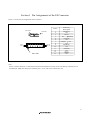
E8 Emulator
Additional Document for User's Manual
R0E000080KCE00EP3
Renesas Microcomputer Development Environment System
M16C Family / M16C/Tiny Series
Notes on Connecting the M16C/26, M16C/26A, M16C/28, and
M16C/29
Rev.4.00
November 1, 2006
Keep safety first in your circuit designs!
1. Renesas Technology Corp. puts the maximum effort into making semiconductor products
better and more reliable, but there is always the possibility that trouble may occur with them.
Trouble with semiconductors may lead to personal injury, fire or property damage.
Remember to give due consideration to safety when making your circuit designs, with appropriate measures such as (i) placement of substitutive, auxiliary circuits, (ii) use of nonflammable material or (iii) prevention against any malfunction or mishap.
Notes regarding these materials
1. These materials are intended as a reference to assist our customers in the selection of the
Renesas Technology Corp. product best suited to the customer's application; they do not
convey any license under any intellectual property rights, or any other rights, belonging to
Renesas Technology Corp. or a third party.
2. Renesas Technology Corp. assumes no responsibility for any damage, or infringement of any
third-party's rights, originating in the use of any product data, diagrams, charts, programs,
algorithms, or circuit application examples contained in these materials.
3. All information contained in these materials, including product data, diagrams, charts, programs and algorithms represents information on products at the time of publication of these
materials, and are subject to change by Renesas Technology Corp. without notice due to
product improvements or other reasons. It is therefore recommended that customers contact
Renesas Technology Corp. or an authorized Renesas Technology Corp. product distributor
for the latest product information before purchasing a product listed herein.
The information described here may contain technical inaccuracies or typographical errors.
Renesas Technology Corp. assumes no responsibility for any damage, liability, or other loss
rising from these inaccuracies or errors.
Please also pay attention to information published by Renesas Technology Corp. by various
means, including the Renesas Technology Corp. Semiconductor home page (http://
www.renesas.com).
4. When using any or all of the information contained in these materials, including product data,
diagrams, charts, programs, and algorithms, please be sure to evaluate all information as a
total system before making a final decision on the applicability of the information and
products. Renesas Technology Corp. assumes no responsibility for any damage, liability or
other loss resulting from the information contained herein.
5. Renesas Technology Corp. semiconductors are not designed or manufactured for use in a
device or system that is used under circumstances in which human life is potentially at stake.
Please contact Renesas Technology Corp. or an authorized Renesas Technology Corp.
product distributor when considering the use of a product contained herein for any specific
purposes, such as apparatus or systems for transportation, vehicular, medical, aerospace,
nuclear, or undersea repeater use.
6. The prior written approval of Renesas Technology Corp. is necessary to reprint or reproduce
in whole or in part these materials.
7. If these products or technologies are subject to the Japanese export control restrictions, they
must be exported under a license from the Japanese government and cannot be imported
into a country other than the approved destination.
Any diversion or reexport contrary to the export control laws and regulations of Japan and/ or
the country of destination is prohibited.
8. Please contact Renesas Technology Corp. for further details on these materials or the
products contained therein.
Contents
Section 1 Specifications of the E8 Emulator ............................................................................................................1
Section 2 Connecting the Emulator with the User System ......................................................................................3
Section 3 Pin Assignments of the E8 Connector .....................................................................................................5
Section 4 Example of E8 Connection ......................................................................................................................7
Section 5 Notes on Using the E8 Emulator............................................................................................................11
Section 6 Setup the Debugger ...............................................................................................................................18
Section 7 Applicable Tool Chain and Partner Tools ..............................................................................................21
This user’s manual is applicable to the E8 emulator software V.2.09 Release 00 or later.
Section 1 Specifications of the E8 Emulator
Table 1.1 shows the specifications of the M16C/Tiny Series E8 Emulator.
Table 1.1 Specifications of the M16C/Tiny Series E8 Emulator
Target MCU
M16C/ Family M16C/Tiny Series
M16C/26, M16C/26A, M16C/28 and M16C/29 Groups
Usable operating mode
Single-chip mode
Break function
- Address match break, 6 points
- PC break (up to 255 points)
- Forcible break
Trace function
Not available
Flash memory programming function
Available
User interface
Clock-synchronized serial (communicating via P64/P65/P66/P67)
MCU resource to be used
- ROM 2KB (alterable assinged address)
- RAM 128bytes (alterable assigned address)
- Stack 14bytes
- UART1 and P64/P65/P66/P67
- P86/Xcout pin or P85/NMI/SDI pin, and P16 pin
- Address match interrupt
Emulator power supply
Interface with host machine
Unnecessary (USB bus powered, power supplied from the PC)
USB (USB 1.1, full speed)
* Also connectable to host computers that support USB 2.0
Power supply function
Can supply 3.3V or 5.0V to the target board (300mA, max)
Power voltage
M16C/26
*1
Normal version
3.0 to 5.5V (f(BCLK)=20MHz)
M16C/28
T version
3.0 to 5.5V
M16C/29
V version
4.2 to 5.5V
2.7 to .5V (f(BCLK)=10MHz)
M16C/26A
[*1] M16C/26B of the M16C/26A group: 24MHz
M16C/28B of the M16C/28 group: 24MHz
Table 1.2 shows the operating environment of the E8 Emulator.
Table 1.2 Operating Environment
Temperature
Humidity
Vibration
Ambient gas
Operating
: 10°C to 35°C
Storage
: –10°C to 50°C
Operating
: 35% RH to 80% RH, no condensation
Storage
: 35% RH to 80% RH, no condensation
Operating
: 2.45 m/s max.
2
2
Storage
: 4.9 m/s max.
Transportation
: 14.7 m/s max.
2
No corrosive gas
1
2
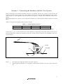
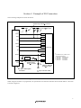
Section 2 Connecting the Emulator with the User System
Before connecting an E8 emulator (hereafter referred to as emulator) with the user system, a connector must be
installed in the user system so that a user system interface cable can be connected. When designing the user system,
refer to Figure 3.1, Pin Assignments of the E8 Connector, and Figure 4.1, Example of E8 Connection, shown in this
manual.
Before designing the user system, be sure to read the E8 emulator user’s manual and the hardware manual for related
MCUs.
Table 2.1 shows the recommended connector for the emulator.
Table 2.1 Recommended Connector
14-pin connector
Type Number
7614-6002OO*
Manufacturer
3M Limited
Specifications
14-pin straight type
*OO indicates coat specification
Connect pins 2, 6, 10, 12, and 14 of the user system connector to GND firmly on the PCB. These pins are used as
electrical GND and to monitor the connection of the user system connector. Note the pin assignments of the user
system connector.
User system interface cable
Connector
User system
Pin 2
Pin 1
Figure 2.1 Connecting the User System Interface Cable to the User System
Notes:
1.
2.
Do not place any components within 3 mm of the connector.
When using the E8 emulator as a programmer, connect the E8 emulator to the user system in the same
way.
3
4
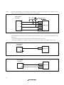
Section 3 Pin Assignments of the E8 Connector
Figure 3.1 shows the pin assignments of the connector.
Pin 1 mark
Connector
Pin NO.
M16C/Tiny
MCU signals
1
P65(SCLK)
2
Vss
3
CNVss.
N.C.
P85(EPM)
4
5
6
7
Pin 2
Pin 14
Pin 1
Pin 13
Pin 1 mark
P67(TxD)
Vss
P86(CE)
P16
8
Vcc
9
P64(BUSY)
10
Vss
11
P66(RxD)
12
Vss
13
RESET
Vss
14
Figure 3.1 Pin Assignments of the E8 Connector
Note:
Pin 14 is used to check for a connection between the E8 and the user system, and is not directly connected to Vss
inside the E8. Make sure that pin 14 and other pins 2, 6, 10, and 12 are connected to Vss.
5
6
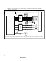
Section 4 Example of E8 Connection
The connecting examples are shown as follows.
Pulled- up at 4.7k Ω or more
Vcc
Vcc
Pulled- up at
4.7k Ω or more
Vcc
Vcc
Vcc
SCLK
P 65
RxD
P 66
TxD
P 67
BUSY
P 64
*1
EPM
P 85
M 16C/ Tiny
*1
CE
P 86 or P16
CNVss
CNVss
Vcc
*
User
logic
RESET
RESET
Vss
*1:
For EPM and CE , select one of
the following settings
(1 ) EPM- P 85: Disconnected
CE- P 86:
Connected
(2 ) EPM- P 85: Connected
Connected
CE- P16:
Pulled- up at
4.7k Ω or more
Pulled- down at
4.7k Ω or more
14- pin 2. 54mm pitch
connector
*: Open-collector buffer
User system
Figure 4.1 Example of E8 Connection
When using the emulator as a programmer, the specification of connection between the E8 and the MCUs is the same
as shown in Figure 4.1.
7
Notes: 1. P64, P65, P66 and P67 pins are used by the E8 emulator. Connect the E8 emulator to the MCU pins. For
MCU pins P65, P66 and P67, pull up and connect to the emulator.
User system
connector
Vcc
Vcc
Vcc
Pulled-up at
4.7kΩ or more
P65
1
P65/ SCLK
5
P67/ TxD
P67
M16C/ Tiny
11
P66
P66/ RxD
9
P64
P64/ BUSY
Figure 4.2 Connection of E8 Emulator and MCUs
2. The E8 emulator uses the P86 or P85, and P16 pins for the MCU control. Connect the E8 emulator to the
MCU pins.
* If the P86 and CE pins are connected, the sub-clock function cannot be used.
* If the P85 and EPM pins and the P16 and CE pins are connected, respectively, NMI cannot be used.
User system
connector
CE
7
P86/ CE
M16C/ Tiny
EPM
Figure 4.3.1 Connection of E8 Emulator and P86 Pin
User system
connector
CE
7
4
EPM
P16
M16C/ Tiny
P85/ EPM
Figure 4.3.2 Connection of E8 Emulator and P85 and P16 Pins
8
3. The E8 emulator uses the CNVss pin for the MCU control. Connect the E8 emulator to the MCU pins
through pull-down.
User system
conncetor
CNVss
Pulled-down at
4.7kΩ or more
3
CNVss
M16C/ Tiny
Figure 4.4 Connection of E8 Emulator and CNVss Pin
4. The RESET pin is used by the E8 emulator. Therefore use an open-collector output buffer or a CR reset
circuit as the reset circuit of the user system. The recommended pull-up value is 4.7kΩ or more. The MCU
can be reset by outputting “L” from the E8 emulator. However, if a reset circuit on the user system is the
H-output type reset IC, it cannot be set “L” in the reset circuit on the user system and the E8 emulator will
not operate normally.
User system
connector
RESET
Vcc
User
logic
*
13
RESET
M16C/ Tiny
Pulled-up at
4.7kΩ or more
*: Open-collector buffer
Figure 4.5 Example of a Reset Circuit
5.
6.
7.
8.
Connect Vss and Vcc with the Vss and Vcc of the MCU, respectively.
Connect nothing with N.C.
The amount of voltage permitted to input to Vcc must be within the guaranteed range of the MCU.
Pin 14 is used to check for a connection between the E8 and the user system, and is not directly connected
to Vss inside the E8. Make sure that pin 14 and other pins 2, 6, 10, and 12 all are connected to Vss.
9
9. Figure 4.6 shows the interface circuit in the E8 emulator. Use this figure as a reference when determining
the pull-up resistance value.
User system connector
Power supply circuit
(Use only with power supply mode)
10kΩ
[*1]
100kΩ
74LVC125A
Emulator control circuit
100kΩ
Vcc
8
22Ω
SCLK
1
22Ω
CNVss
3
22Ω
EPM
4
22Ω
CE
7
22Ω
RxD
11
100kΩ
1MΩ
100kΩ
74LVC125A
100kΩ
100kΩ
22Ω
TxD
22Ω
BUSY
22Ω
RESET
5
9
13
3.3V
10kΩ
2SC2462
10kΩ
[*1] Power of the upper 74LVC125A is supplied from Vcc in the user system connector or power supply circuit (with power supply mode).
Figure 4.6 Interface Circuit in the Emulator (Reference)
10
Section 5 Notes on Using the E8 Emulator
1. Program area for the E8 emulator
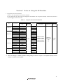
Table 5.1 lists the program area for the E8 emulator.
Do not change this area. If this area is changed, the E8 emulator will not operate normally. In this case, disconnect
to the debugger and then reconnect.
Table 5.1 Program Area for the E8 Emulator
ROM size
Group
M16C/26
M16C/26A
M16C/28
M16C/29
Program Area for E8 Emulator
Type Number
Programming
Area
M30262F3
24KB
1KB
M30262F4
32KB
1KB
M30262F6
48KB
2KB
M30262F8
64KB
2KB
M30260F3
24KB
1KB
M30260F6
48KB
2KB
M30260F8
64KB
2KB
M30263F3
24KB
1KB
M30263F6
48KB
2KB
M30263F8
64KB
2KB
M30280F6
48KB
4KB
M30280F8
64KB
M30280FA
96KB
8KB
M30280FC
128KB
12KB
M30281F6
48KB
4KB
M30281F8
64KB
4KB
M30281FA
96KB
8KB
M30281FC
128KB
12KB
M30290FA
96KB
8KB
M30290FC
128KB
12KB
Data Area
4KB
RAM size
4KB
M30291FA
96KB
8KB
M30291FC
128KB
12KB
Vector Area
ROM Area
RAM Area
2KB of the
programming
area
128KB
FFFE4h--FFFE7h,
FFFE8h--FFFEBh,
FFFECh--FFFEFh,
FFFF4h--FFFF7h,
[*1]
[*1]
FFFFCh--FFFFFh
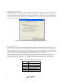
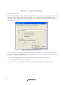
*1: When the debugger is initiated, [Emulator Setting] dialog box shown in Figure 5.1 is displayed. Specify an area
which is not used in the user system.
11
Figure 5.1 [Firmware Location] tab of [Emulator Setting] dialog box
2. When the emulator system is initiated, it initializes the general registers and part of the flag registers as shown in
Table 5.2.
Table 5.2 Register Initial Values at Emulator Power-On
Status
Register
Initial Value
E8 Emulator PC
Reset vector value in the vector address table
Power-On
R0 to R3 (bank 0, 1) 0000h
A0, A1 (bank 0, 1)
0000h
FB (bank 0, 1)
0000h
INTB
0000h
USP
0000h
ISP
Work RAM Address for the E8 emulator + 80h *
SB
0000h
FLG
0000h
Note: The Work RAM address for the E8 emulator is specified in [Firmware Location] tab in [Emulator Setting] dialog box.
3. The emulator controls the MCUs by using the P64, P65, P66, P67, RESET , CNVss pins, and P86 or P85 and P16
pins.
4. The emulator uses up to 14bytes stack pointer when a user program breaks. Accordingly, reserve the 14bytes
addresses for the stack area.
12
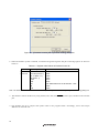
5. SFR used by the program for the E8 emulator
As the SFR listed in Table 5.3 is used by the program for the E8 emulator, do not change a value. Otherwise, the E8
emulator cannot be controlled. Note that UART1 transmit interrupt control register S1TIC and UART1 receive
interrupt control register S1RIC always read out the value of using the emulator. And they are not initialized by
selecting [Debug] -> [Reset CPU] or with the RESET command. If their contents are referred to, a value that has
been set in the program for the E8 emulator will be read.
Table 5.3 SFR Used by Program for E8 Emulator
Address
Register
Symbol
Bit
Notes on using
the E8 emulator
0009h
Address match interrupt enable register
AIER
All bits
[*1]
0010h - 0012h
Address match interrupt register 0
RMAD0
All bits
[*1]
0014h - 0016h
Address match interrupt register 1
RMAD1
All bits
[*1]
03A8h
UART1 transmit/receive mode register
U1MR
All bits
[*1]
03AAh, 03ABh
UART1 transmit buffer register
U1TB
All bits
[*1]
03ACh
UART1 transmit/receive control register 0
U1C0
All bits
[*1]
03ADh
UART1 transmit/receive control register 1
U1C1
All bits
[*1]
03AEh, 03AFh
UART1 receive buffer register
U1RB
All bits
[*1]
03B0h
UART transmit/receive control register 2
UCON
Bits 1, 3, 4, 5 and 6
[*2]
03ECh
Port P6 register
P6
Bits 4, 5, 6 and 7
[*2]
03EEh
Port P6 direction register
PD6
Bits 4, 5, 6 and 7
[*2]
025Dh
Pin Assignment Control Register [*3]
PACR
Bit 7
[*2]
*1 Do not change the value of the register.
*2 Do not change the value of the bits listed above. When operating this register, change it by a bit operating
instruction, etc. in order to avoid changing the value of relevant bits.
*3 Not included in the M16C/26 group.
6. Interrupts used by the E8 emulator program
The BRK instruction interrupt, address match interrupt, single-step interrupt, and DBC interrupt are used by the E8
emulator program. Therefore, make sure the user program does not use these interrupts. The E8 emulator changes
these interrupt vector values to the values to be used by the emulator. It is not a problem if the interrupt vector
values are written in the user program.
13
7. Debugging of the watchdog timer
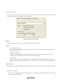
When debugging the user program using the watchdog timer, select the [Debugging of program that uses WDT.]
check box in the [Firmware Location] tab of [Emulator Setting] dialog box. By selecting this box, the program for
the E8 emulator refreshes the watchdog timer during program operation. If a memory is accessed by the memory
reference or modification, the watchdog timer will be refreshed by the program for the E8 emulator. Note that the
operation timing is different from the actual one.
Figure 5.2 [Firmware Location] tab of [Emulator Setting] dialog box
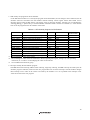
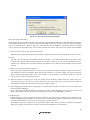
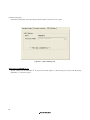
8. ID code of flash memory
This is the function of the MCUs which prevents the flash memory from reading out by other than the user. The 7
bytes ID code in Table 5.4 written to the flash memory of the MCUs have to match with the ID code displayed in
Figure 5.3 [ID Code verification] dialog box at the debugger startup, otherwise the debugger cannot be started up.
Note that when the ID code is FFh, FFh, FFh, FFh, FFh, FFh, FFh, ID code is considered not set up. In this case, the
ID code is automatically authenticated and [ID Code verification] dialog box is not displayed.
When debugging in [Erase Flash and Connect] mode or [Keep Flash and Connect] mode, the ID code, FFh, FFh,
FFh, FFh, FFh, FFh, FFh is written into the ID code area regardless of the contents of the user program. In
[Program Flash] mode, the value to be written in the ID code area depends on the contents of the user program.
Table 5.4 ID Code Storage Area of M16C/Tiny
Address
FFFDFh
FFFE3h
FFFEBh
FFFEFh
FFFF3h
FFFF7h
FFFFBh
14
Description
First byte of ID code
Second byte of ID code
Third byte of ID code
Fourth byte of ID code
Fifth byte of ID code
Sixth byte of ID code
Seventh byte of ID code
Figure 5.3 [ID Code verification] Dialog Box
[Note on Program Flash mode]
When the ID code is specified by the -ID option of the lmc30, download the MOT file or HEX file. When the X30 file
is downloaded, the ID code is not effective. When downloading the X30 file, specify the ID code using an assembler
directive command such as “.BYTE”. The file to which the ID code specified by the assembler directive command
“.ID” is output varies depending on the version of the assembler. For details, refer to the user’s manual of the assembler.
9. Operation clock while the user program remains idle
While the user program remains idle, the E8 emulator program changes the main clock divide-by-N value as it runs.
10. Reset
The reset vector is used by the E8 emulator program. If the MCU is reset while executing the user program, control
is transferred to the E8 emulator program and the user program is made to stop. Do not use the hardware reset 2,
software reset, watchdog timer reset and oscillation stop detection reset, otherwise the E8 emulator will not operate
normally.
11. Memory access during emulation execution
When referring or modifying the memory contents, the user program is temporarily halted. For this reason, the realtime emulation cannot be performed. When the real-time emulation is necessary during the program operation,
firstly disable the automatic update in the watch window or fix the display in the memory window so that the
memory access will not occur during execution.
12. When the E8 does not supply power to the user system, the E8 emulator consumes the power voltage of the user
system from several mA to over 10 mA. This is because the user power supply drives one 74LVC125A to make the
communication signal level match the user system power supply voltage.
13. When debugging, the flash memory is frequently re-written by the E8 emulator. Therefore, do not use an MCU that
has been used for debugging.
Also, as the program for the E8 emulator is written into the MCUs while debugging, do not save the contents of the
MCU’s flash memory that have been used for debugging or use them as the ROM data for products.
14. NMI interrupt
If NMI interrupts are to be used, be sure to take the necessary measures before executing the user program by, for
example, disabling automatic updates of the watch window and freezing the display of the memory window in order
to ensure that no memory accesses will occur during user program execution.
If an NMI interrupt occurs while the user program remains idle or when memory contents are referenced or changed
during user program execution, device operation becomes uncontrollable by the E8 emulator.
15
15. Reserved area
The addresses not specified in the Hardware Manual for M16C/26, M16C/26A, M16C/28, and M16C/29 Groups
are reserved area. Do not change the contents. Otherwise, the E8 emulator cannot be controlled.
16. Debugging in stop mode or wait mode
When debugging in the stop or wait mode, the program cannot be stopped by the E8 emulator. If you attempt to
stop the program during the stop or wait mode, the emulator will be uncontrollable.
Do not operate the window until the program stops at the breakpoint by setting the breakpoint at the processing unit
where the stop mode or wait mode is cancelled. When using the stop mode or wait mode on a user program, firstly
disable the automatic update in the watch window or fix the display in the memory window so that the memory
access will not occur during execution.
17. Peripheral I/Os during a break
During a break, although interrupts are not accepted, peripheral I/Os continue to be operated. For example, a timer
interrupt is not accepted although counting a timer is continued when a user program is stopped by a break after
operating a timer.
18. Exceptional step operation
a) Software-interrupt instruction
STEP operation cannot be performed by continuously executing the internal processing of instructions
(undefined, overflow, BRK, and INT) which generates a software interrupt.
<Example> INT instruction
NOP
NOP
INT#3
NOP
JMP MAIN
Passes through if the STEP operation is carried out.
INT_3:
NOP
NOP
NOP
REIT
The address at which the program should be stopped.
b) INT instruction
Debugging of the program using the INT instruction should be used with the GO command by setting a PC
break for the internal processing of the INT instruction.
<Example>
NOP
INT #3
NOP
JMP MAIN
INT_3:
NOP Break
NOP
REIT
16
Execution with the GO command
19. “Go to cursor” function
The "Go to cursor" function is realized by using an address match break. Therefore, when you execute the "Go to
cursor" command, all the address match breaks you set become invalid, while all the PC breaks remain valid.
20. Notes on PC break point
When downloading a user program after changing it, the address setting of a PC break may not be corrected
normally depending on the changes. After downloading a user program, please check the setting of a PC break by
event point window and reset it.
21. Notes on debugging in CPU rewrite mode
When debugging in CPU rewrite mode, do not rewrite the CPU’s block 0 area (addresses FE000h – FFFFFh) and
block containing the program for the E8 emulator. If these areas are rewritten, the E8 emulator will run out of
control.
Do not halt the user program after setting the CPU rewrite mode until releasing it. If you do so, the E8 emulator
may run out of control. Cancel the automatic renewal in the watch window in advance and select fixing display in
the memory window to prevent a memory access from occurring while executing the user program.
To check the data after executing the CPU rewrite mode, halt the program after releasing the CPU rewrite mode and
see the memory window etc.
When rewriting the flash memory in the program area, select Menu of the High-performance Embedded Workshop
– [Setup] -> [Emulator] -> [System...] to open [Configuration] dialog box. In this dialog box, change [Flash
memory synchronization] setting to [Flash memory to PC] and set off the cash of the debugger. In this setting, the
flash memory is read whenever a break occurs, which takes some time. Use it with [Disable] setting except when
debugging in CPU rewrite mode.
22. Notes on rewriting the flash memory
Do not reset the MCUs when rewriting the flash memory. The flash memory is completed to rewrite when the
“Flash memory write end” is displayed in the output window of the High-performance Embedded Workshop. If the
MCU is reset during rewriting the flash memory, the user program or the program for the E8 emulator may be
disrupted
The followings indicate when the flash memory rewrite occurs.
- When downloading the user program
- After the user program starts with setting up PC break on the flash memory
- After the user program starts with canceling PC break on the flash memory
- After the user program starts with rewriting the value of flash memory in the memory window
23. Notes on the E8 emulator power supply
When writing reliability required program with the E8 emulator under the mass production, do not use the E8
emulator power supply function. Separately supply appropriate voltage according to the MCU programming to the
user system. Since the supplied voltage from the E8 emulator depends on the quality of the USB power supply of
the PC, its precision is not guaranteed.
24. Notes on the emulator setup switch
Use the emulator setup switch with the factory setting (upper side “1”).
17
Section 6 Setup the Debugger
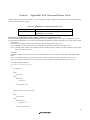
(1) Emulator Setting dialog box
[Emulator Setting] dialog box is provided for setting the items that need to be set when the debugger starts up. The
contents set from this dialog box other than “Power supply” are also effective the next time the debugger starts.
When starting up the debugger first time after creating the new project work space, [Emulator Setting] dialog box is
displayed with the Wizard.
Figure 6.1 [Emulator Setting] dialog box.
To keep the [Emulator Setting] dialog box closed the debugger is started next time, check "Do not show this dialog
box again." at the bottom of the [Emulator Setting] dialog box. You can open the [Emulator Setting] dialog box
using either one of the following methods:
- After the debugger gets started, select Menu - [Setup] -> [Emulator] -> [Emulator Setting (E)...].
- Start Debugger while holding down the Ctrl key.
When you check the "Do not show this dialog box again.", the E8 does not supply power to the user system.
18
(2) Emulator mode Tab
The selection of the device, the specification of the mode, and the setting of the power supply are done in the
[Emulator mode] tab of the [Emulator Setting] dialog box.
Figure 6.2 [Emulator mode] Tab
[Device]
Select the name of the MCUs to be used from the [Device] drop-down list box.
[Mode]
- Erase Flash and Connect
When starting up the debugger, erase the flash memory data of the MCUs. The program for the E8 emulator is
written at the same time.
- Keep Flash and Connect
When starting up the debugger, keep the flash memory data of the MCUs. Note that the area for the E8
emulator program and the E8 emulator used vector area will be changed.
- Program Flash
Select this mode when using the E8 emulator as a simple programmer. On downloading write only the user
program (The program for the E8 emulator is not written). Therefore, the program cannot be debugged in this
mode.
[Power supply]
When [Power Target from E8. (MAX 300mA)] is checked, power will be supplied to the user system up to 300mA.
(3) Firmware Location Tab
For details, see “1. Program area for the E8 emulator” and “7. Debugging of the watchdog timer” of the “Section 5.
Notes on Using the E8 Emulator”.
19
(4) MCU Setting Tab
In the MCU Setting tab, set the operating condition of MCU used in the user system.
Figure 6.3 [MCU Setting] Tab
PM10 (bit 0 of 000005H) is “1”
Specify whether you set the PM10 (0th bit of processor mode register 1). When using your system with the setting
that PM10 is 1, check this option.
20
Section 7 Applicable Tool Chain and Partner Tools
With the M16C/Tiny Series E8 emulator, you can debug a module created by the inhouse tool chain and third-party
products listed in Table 7.1 below.
Table 7.1 Applicable Tool Chain and Partner Tools
Tool chain
Partner tools
M3T-NC30WA V.5.20 Release 01 or later
TASKING M16C C/C++/EC++ Compiler V.2.3r1 or later
IAR EWM16C V.2.12 or later
[Precautions on debugging the load modules created in ELF/DWARF2 format]
If the load module was created in ELF/DWARF2 format using TASKING M16C C/C++/EC++ compiler V3.0r1, the
precaution described below must be observed when displaying member variables of the base class in the watch window.
<Precaution>
If any class object that has a base class is defined, the following problems may occur:
Case 1: Member variables of the base class cannot directly be referenced from the class object (*1).
Case 2: If the PC value resides in any member function of a derived class, member variables of the base class cannot
directly be referenced (*4).
<Solution>
If member variables of the base class need to be referenced in the watch window, follow either method described
below.
Case 1: Use indirect references from the class object to refer to member variables of the base class (*2) (*3).
Case 2: Use indirect references from “this” pointer to refer to member variables of the base class (*5) (*6).
<Example program statement>
/////////////////////////////////////////////////////////
*.h
class BaseClass
{
public:
int m_iBase;
public:
BaseClass() {
m_iBase = 0;
}
void BaseFunc(void);
};
class DerivedClass : public BaseClass
{
public:
int m_iDerive;
public:
DerivedClass() {
m_iDerive = 0;
}
void DerivedFunc(void);
21
};
*.cpp
main()
{
class DerivedClass ClassObj;
ClassObj.DerivedFunc();
return;
}
void BaseClass::BaseFunc(void)
{
m_iBase = 0x1234;
}
void DerivedClass::DerivedFunc(void)
{
BaseFunc();
m_iDerive = 0x1234;
}
/////////////////////////////////////////////////////////
<Example for registering in the watch window>
/////////////////////////////////////////////////////////
Case 1: If the PC value resides in the main() function
(1)"ClassObj.m_iBase"
: Cannot be referenced (*1)
(2)"ClassObj.__b_BaseClass.m_iBase"
: Can be referenced (*2)
(3)"ClassObj"
-"__b_BaseClass"
: Can be referenced (*3)
-"m_iBase"
-"m_iDerive"
-: Expansion symbol
Case 2: If the PC value resides in the DerivedClass::DerivedFunc() function
(1)"m_iBase"
: Cannot be referenced (*4)
(2)"this->__b_BaseClass.m_iBase" : Can be referenced (*5)
(3)"__b_BaseClass.m_iBase"
: Can be referenced (*5)
(4)"this"
-"*"
-"__b_BaseClass"
: Can be referenced (*6)
-"m_iBase"
-"m_iDerive"
(5)"__b_BaseClass"
-"m_iBase"
: Can be referenced (*6)
/////////////////////////////////////////////////////////
22
E8 Emulator
Additional Document for User's Manual
Notes on Connecting the M16C/26, M16C/26A, M16C/28, and M16C/29
Publication Date:
April 1, 2005
November 1, 2006
Rev.1.00
Rev.4.00
Published by:
Sales Strategic Planning Div.
Renesas Technology Corp.
Edited by:
Microcomputer Tool Development Department
Renesas Solutions Corp.
© 2006. Renesas Technology Corp. and Renesas Solutions Corp., All rights reserved. Printed in Japan.
E8 Emulator
Additional Document for User's Manual