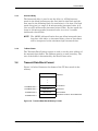
1
DAS-429P104/Mx MULTI-CHANNEL ARINC-429 Test and Simulation Board for PC/104 Computers User’s Manual 311 Meacham Avenue Elmont, NY 11003 Tel. (516) 327-0000 Fax (516) 327-4645 e-mail: [email protected] website: www.mil -1553.com Contents Contents 1 Introduction ................................................................................1-1 1.1 Overview...............................................................................1-1 1.2 Installation ............................................................................1-4 1.3 General Memory Map ...........................................................1-5 1.4 Global Registers ...................................................................1-6 1.4.1 Global Bank Select Register ........................................................................ 1-6 1.4.2 Global Software Reset Register ................................................................... 1-6 1.4.3 Global Interrupt Reset Register .................................................................... 1-7 1.4.4 Global Interrupt Status Register ................................................................... 1-7 2 Module Operation ......................................................................2-1 2.1 Module General Operation ...................................................2-1 2.2 Module Memory Map.............................................................2-3 2.3 Module Control Registers .....................................................2-4 2.3.1 Start/Stop Register ....................................................................................... 2-4 2.3.2 Module Status Register ................................................................................ 2-5 2.3.3 Firmware Revision Register........................................................................... 2-6 2.3.4 Channel Interrupt Register ........................................................................... 2-6 2.3.5 Receiver Data Storage Mode Register........................................................... 2-7 2.3.6 Interrupt Status Busy Register...................................................................... 2-8 2.3.7 Reset Time Tag Register.............................................................................. 2-8 2.3.8 Module ID Register....................................................................................... 2-8 2.4 Receiver Merge Mode Control Registers..............................2-9 2.4.1 Receiver Merge Start Pointer ....................................................................... 2-9 2.4.2 Receiver Merge End Pointer ........................................................................ 2-9 2.4.3 Receiver Merge Current Pointer................................................................... 2-9 2.4.4 Receiver Merge Filter Table Start Address .................................................. 2-9 2.4.5 Receiver Merge Word Counter..................................................................... 2-9 2.4.6 Receiver Merge Buffer Wraparound Register ............................................ 2-10 2.4.7 Receiver Merge Word Count Trigger Register ........................................... 2-10 2.4.8 Receiver Merge Interval Count Trigger Register ........................................ 2-10 2.4.9 Receiver Merge Label Trigger Register...................................................... 2-11 2.4.10 Receiver Merge Configuration Register ................................................... 2-11 2.4.11 Receiver Merge Interrupt Condition Register ........................................... 2-12 2.4.12 Receiver Merge Status Register............................................................... 2-13 3 Transmit Mode ...........................................................................3-1 3.1 Transmit Channel Control Register Block Maps...................3-1 3.1.1 Channel 2 Control Register Block Map ........................................................ 3-1 3.1.2 Channel 5 Control Register Block Map ........................................................ 3-2 3.2 Transmit Channel Control Registers.....................................3-2 3.2.1 Channel x Configuration Register................................................................. 3-2 3.2.2 Channel x Tx Instruction Stack Pointer ........................................................ 3-3 3.2.3 Channel x Tx Instruction Counter ................................................................. 3-3 3.2.4 Channel x Tx Loop Counter.......................................................................... 3-3 3.2.5 Channel x Tx Current Word Register ........................................................... 3-4 3.2.6 Channel x Tx Current Loop Register ............................................................ 3-4 3.2.7 Channel x Interrupt Condition Register ........................................................ 3-4 3.2.8 Channel x Status Register............................................................................ 3-5 DAS-429P104/Mx User's Manual page i Contents 3.3 Transmit Instruction Stack ....................................................3-5 3.3.1 Control Word Definition ................................................................................ 3-6 3.3.2 Word Count .................................................................................................. 3-6 3.3.3 Interword Delay ............................................................................................ 3-7 3.3.4 Tx Data Pointer............................................................................................. 3-7 3.4 Transmit Data Block Format .................................................3-7 4 Receive/Monitor Mode ...............................................................4-1 4.1 General Information..............................................................4-1 4.1.1 Sequential Mode Overview........................................................................... 4-1 4.1.2 Look-Up Table Mode Overview .................................................................... 4-2 4.1.3 Merge Mode Overview.................................................................................. 4-2 4.2 Sequential/Merge Mode Operation.......................................4-2 4.2.1 Receive Buffer Storage Sequence ............................................................... 4-2 4.2.2 Rcv Data Word Format................................................................................. 4-3 4.2.3 Time Tag Word Description.......................................................................... 4-4 4.2.4 Rcv Sequential Mode Filter Table Diagram .................................................. 4-5 4.2.5 Receive Sequential Mode Status Word........................................................ 4-6 4.2.6 Receive Merge Mode Status Word............................................................... 4-6 4.3 Look-Up Table Mode Operation ...........................................4-7 4.3.1 Receive Look-Up Table Storage Sequence ................................................. 4-7 4.3.2 Rcv Look-Up Table Mode Diagram .............................................................. 4-7 4.3.3 Receive Look-Up Table Status/Control Word .............................................. 4-8 4.4 Receive Channel Control Register Block Maps ....................4-9 4.4.1 Channel 0 Control Register Block Map ........................................................ 4-9 4.4.2 Channel 1 Control Register Block Map ...................................................... 4-10 4.4.3 Channel 3 Control Register Block Map ...................................................... 4-11 4.4.4 Channel 4 Control Register Block Map ...................................................... 4-12 4.5 Receive Channel Control Registers....................................4-12 4.5.1 Channel x Configuration Register............................................................... 4-12 4.5.2 Channel x Receive Data Start Pointer........................................................ 4-14 4.5.3 Channel x Receive Data End Pointer ......................................................... 4-14 4.5.4 Channel x Receive Data Current Pointer ................................................... 4-14 4.5.5 Channel x Receive Look-Up Table Start Address ...................................... 4-14 4.5.6 Channel x Receive Filter Table Start Address............................................ 4-15 4.5.7 Channel x Rcv Data Word Count Register ................................................. 4-15 4.5.8 Channel x Rcv Buffer Wraparound Register .............................................. 4-15 4.5.9 Channel x Rcv Data Word Counter Trigger Register ................................. 4-16 4.5.10 Channel x Rcv Interval Counter Trigger Register ..................................... 4-16 4.5.11 Channel x Rcv Label Trigger Register...................................................... 4-16 4.5.12 Channel x Interrupt Condition Register .................................................... 4-17 4.5.13 Channel x Status Register........................................................................ 4-18 5 Mechanical and Electrical Specifications ................................5-1 5.1 Card Layout ..........................................................................5-1 5.2 Jumpers................................................................................5-2 5.2.1 Shield Signal Jumper ................................................................................... 5-2 5.2.2 Base Address Select Jumpers ..................................................................... 5-2 5.2.3 Interrupt Select Jumpers .............................................................................. 5-3 5.2.4 Factory Default Jumpers Settings ................................................................ 5-3 5.3 Connectors ...........................................................................5-4 5.3.1 Connectors J1,J2 Pinout ............................................................................... 5-4 5.3.2 PC/104 Bus Connectors Pinout.................................................................... 5-6 5.4 Power Requirements ............................................................5-7 6 Ordering Information .................................................................6-1 page ii Excalibur Systems, Inc. Contents Figures Figure 1-1. DAS-429P104/Mx Block Diagram .......................................1-3 Figure 1-2. M429R4T2 Module Block Diagram .....................................1-3 Figure 1-3. General Memory Map.........................................................1-5 Figure 2-1. Module M429R4T2 Memory Map........................................2-3 Figure 2-2. Module Control Registers Map ...........................................2-4 Figure 3-1. Channel 2 Control Register Block Map ...............................3-1 Figure 3-2. Channel 5 Control Register Block Map ...............................3-2 Figure 3-3. Tx Instruction Stack Structure ............................................3-6 Figure 3-4. Transmit Data Words Memory Format ................................3-7 Figure 3-5. Data Bytes in Memory ........................................................3-8 Figure 4-1. Rcv Sequential Mode Buffer Structure................................4-3 Figure 4-2. Rcv Data Word Format.......................................................4-3 Figure 4-3. Time Tag Word Description ................................................4-4 Figure 4-4. Rcv Sequential Mode Filter Table .......................................4-5 Figure 4-5. Label Control Byte Structure (WRITE)................................4-5 Figure 4-6. Rcv Look-Up Table Mode Structure ....................................4-7 Figure 4-7. Channel 0 Control Register Block Map ...............................4-9 Figure 4-8. Channel 1 Control Register Block Map .............................4-10 Figure 4-9. Channel 3 Control Register Block Map ............................. 4-11 Figure 4-10. Channel 4 Control Register Block Map ...........................4-12 Figure 5-1. Card Layout .......................................................................5-1 Figure 5-2. Base Address Select Jumpers............................................5-2 Figure 5-3. Connectors J1,J2 Layout (Front View) ................................5-4 DAS-429P104/Mx User's Manual page iii Contents Tables Table 5-1. Interrupt Select Jumpers......................................................5-3 Table 5-2. Connectors J1,J2 Pin Assignments......................................5-5 Table 5-3. J1,J2 Signals Description.....................................................5-5 Table 5-4. Connectors PC/104 Bus Pinout............................................5-6 page iv Excalibur Systems, Inc. Contents What is in this manual? This manual is divided into the following six chapters: Chapter 1, “Introduction,” provides an overview of the DAS-429P104/Mx board and discusses card installation, external connections, the memory usage and card registers. Chapter 2, “Module Operation,” describes the general principle of module operation, the module memory map, and the module control registers. Chapter 3, “Transmit Mode,” explains how to implement transmitter operation, and describes transmit channel control register block maps, transmit channel control registers, the transmit instruction stack, and the transmit data block format. Chapter 4, “Receive/Monitor Mode,” describes the general principle of receiver/monitor operation. This includes a description of sequential/merge mode and look-up table mode operation, receive channel control register block maps, and receive channel control registers. Chapter 5, “Mechanical and Electrical Specifications,” describes the mechanical and electrical specifications of the DAS-429P104/Mx board. This includes a description of board layout, board case ground, jumpers, connectors, and power requirements. Chapter 6, “Ordering Information,” explains how to indicate which options you want when ordering a DAS-429P104/Mx card. DAS-429P104/Mx User's Manual page v Contents page vi Excalibur Systems, Inc. Introduction 1 Introduction Chapter 1 provides an overview of the DAS-429P104/Mx avionics communication board. The following topics are covered: • • • • 1.1 “Overview,” page 1-1 “Installation,” page 1-4 “General Memory Map,” page 1-5 “Global Registers,” page 1-6 Overview The DAS-429P104/Mx is a modular ARINC-429 memory-mapped, 12 channel test, simulation, and monitor card for PC/104 systems. The DAS-429P104/Mx provides a total solution for developing and testing ARINC-429 interfaces and for performing system simulation of the ARINC-429 bus, both in the lab and in the field. The DAS-429P104/Mx is based on the latest Surface Mount Technology, which substantially reduces the area required. The card occupies 32K bytes of the host computer’s memory map. The DAS429P104/Mx comes configured with 2(x) transmit and 4(x) receive channels (where x = number of modules ordered). The channels are organized in two independent modules (P/N: M429R4T2), each configured with 4 receive and 2 transmit channels. Each module contains an on board hi-speed controller and 16K x 16 true dual-port RAM. Each module is accessed through a banking mechanism and operates independently. You can set up each module to generate interrupts to the host in a variety of circumstances through an extensive interrupt structure. Both transmit and receive channels may be programmed for Hi (100Khz) or Lo (12.5Khz) speed bit rates. In addition, either odd or even parity may be programmed for transmit channels. All control registers and data blocks can be accessed directly in real time. The card supports filtering of receive data and multiple data storage modes. Status and time tag information are appended to each word. The transmit channels operate via a transmitter “instruction” stack which allows scheduling of data transmissions and reduces the need for host computer intervention. The DAS-429P104/Mx comes complete with C-driver software libraries, including source code. The DAS-429P104/Mx is ideally suited for developing, simulating, testing and monitoring ARINC-429 interfaces for multi-channel applications requiring a single PC/104 card. For industrial environment applications the DAS-429P104/Mx is available in an extended temperature (-40° to +85°C) version. See “Ordering Information,” page 6-1 for the exact part numbers. DAS-429P104/Mx User's Manual page 1-1 Introduction DAS-429P104/Mx Card Features: • Up to 8 Receive and 4 Transmit channels on a PC/104 card • Organized in 2 modules, each containing: • 4 Receive channels • Two Receive/Monitor modes: • Sequential • Look-up table • 32 bit time tagging per word • 16k x16 true dual-port RAM • “Merge mode” stores data from multiple receive channels in one buffer • On board 32 bit processor • Label filtering • 2 Transmit channels • 12.5k bit and 100k bit data rates • Selectable even/odd parity • Start triggers • Receive count interval triggers • Programmable interword gap • Interrupt and polling modes of operation • Transmission modes: • PC/104 compliance: • One-shot • Loop • “N”- times • Occupies 32K (1/2 segment) of the memory map • All interrupt lines selectable • Real time operation • Extended temperature (-40° to +85° C) version available page 1-2 Excalibur Systems, Inc. Introduction Figure 1-1 below illustrates the DAS-429P104/Mx’s block diagram. Figure 1-1. DAS-429P104/Mx Block Diagram Figure 1-2 below illustrates the block diagram of a single M429R4T2 module. Figure 1-2. M429R4T2 Module Block Diagram DAS-429P104/Mx User's Manual page 1-3 Introduction 1.2 Installation Before installing the card, it is very important to determine which halfsegment of memory is available. Programs such as Symantec Corporation’s SYSINFO.EXE or Microsoft Corporation’s MSD.EXE may be used to determine which memory segments are in use by the BIOS and any other adapter cards already installed on your computer. WARNING If a segment is already in use and it is also used for DAS-429P104/Mx, the card will exhibit unpredictable behavior. It may work in some modes, but not others; it may seem to work fine yet exhibit intermittent errors; it may not function at all. Once a free segment is found, the Base Address Select jumpers (JP12-JP16) should be set accordingly. The Interrupt Select jumpers (JP17-JP27) should be set to the required interrupt line, if using interrupts. Once all the jumpers are correctly set, make certain the computer power source is disconnected. While using a suitably grounded electrostatic discharge wrist strap, install the DAS-429P104/Mx card on top of the other cards in your system. Once the card is installed, the mating 16-pin header socket—wired with the ARINC-429 connections—should be attached to the card. page 1-4 Excalibur Systems, Inc. Introduction 1.3 General Memory Map The DAS-429P104/Mx occupies 32K bytes of the host computer’s memory map. This is divided into two sections: Module Memory Area and four Global Registers. The Module Memory Area contains 64Kb of dual-port RAM divided into 2 banks of 32Kb each. You can change banks via the Global Bank Select Register defined below. The Global Registers are independent of the selected bank, and include appropriate control bits for all the banks (Modules). Global Bank Select Register 0000 H Global Software Reset Register 0002 H Global Interrupt Reset Register 0004 H Global Interrupt Status Register 0006 H Reserved 0008–000E H Module_0 Memory Area Module_1 Memory Area BANK # 0 BANK # 1 0010–7FFF H Figure 1-3. General Memory Map DAS-429P104/Mx User's Manual page 1-5 Introduction 1.4 Global Registers 1.4.1 Global Bank Select Register Address: 0000 (H) READ/WRITE The Global Bank Select register sets the Bank Select for the desired Module access. Writing a zero will give the host access to bank 0, and 1 to bank 1. This register is set to 0 at power-up. WRITE DEFINITION Bit Bit Name 01-15 X - Don’t Care 00 BS0 0 1 Description Bank 0 (Module_0) Bank 1 (Module_1) READ DEFINITION Bit Bit Name 01-15 X - Don’t Care 00 BS0 Global Bank Select Register 1.4.2 Global Software Reset Register Address: 0002 (H) WRITE The Global Software Reset register is used to reset the card. Writing a value of 1 to the appropriate bit will reset the corresponding Module. Writing a value of 0 has no effect. WARNING Reset erases all memory locations in the dual-port RAM. The Module Status, Firmware Revision, Module ID and Channel x RCV Look-Up Table Start Address registers are written by the card after reset operation has been completed. Bit Description 02-15 X - Don’t Care 01 Module_1 Software Reset 00 Module_0 Software Reset Global Software Reset Register page 1-6 Excalibur Systems, Inc. Introduction 1.4.3 Global Interrupt Reset Register Address: 0004 (H) WRITE The Global Interrupt Reset register is used to reset the card interrupt request. Writing a value of 1 to the appropriate bit will reset the corresponding Module interrupt request. Writing a value of 0 has no effect. Bit Description 02-15 X - Don’t Care 01 Module_1 Interrupt Reset 00 Module_0 Interrupt Reset Global Interrupt Reset Register 1.4.4 Global Interrupt Status Register Address: 0006 (H) READ The Global Interrupt Status register indicates the card pending interrupts status. A value of 1 at the appropriate bit indicates a corresponding Module active interrupt. A value of 0 indicates no interrupt has been generated. Bit Description 02-15 X - Don’t Care 01 Module_1 Interrupt Status 00 Module_0 Interrupt Status Global Interrupt Status Register DAS-429P104/Mx User's Manual page 1-7 Introduction page 1-8 Excalibur Systems, Inc. Module Operation 2 Module Operation Chapter 2 describes the general principle of module operation, the module memory map, and the module control registers. The following topics are covered: • • • • “Module General Operation,” page 2-1 “Module Memory Map,” page 2-3 “Module Control Registers,” page 2-4 “Receiver Merge Mode Control Registers,” page 2-9 Each bank (Module) handles 4 receive and 2 transmit channels, is controlled by its own processor and works independently of the other banks. All 12 channels may be run simultaneously although you may only access one bank (six channels) at a time. The manual describes the functionality of a single bank; all banks work in an identical manner. Perform the following procedure after every time you power up or reset the software. To determine whether a module is installed and ready to operate: 1. Check the Module ID register (test for value = E429 H). 2. Check the Module Status Register (see “Module Status Register,” Note 1, page 2-6). The module is installed and ready when both registers contain the correct values (as written above). For software reset operations, set these values to 0 immediately prior to writing to the Card Software Reset register. 2.1 Module General Operation The M429R4T2 module operation makes extensive use of pointers for setting up the size and location of both receiver and transmitter data blocks, transmitter instruction stacks, and receiver look-up tables. Pointers on the card represent byte offsets into the memory area of the card. Each channel has its own pointer registers so that unique memory areas may be allocated for each channel. It is also possible for multiple channels to share memory areas. For example, more than one receiver channel may point to and use the same Label Look-Up Table, which controls which labels will be stored by the card. After power-up or reset the module is initialized in a “wait” loop— looking for a Start command from the host computer. This command, issued by writing to the Module Start Register, instructs the module to begin operation on the active channel(s). DAS-429P104/Mx User's Manual page 2-1 Module Operation The transmitter and receiver operations necessary to operate the card are described below in general terms. See “Transmit Mode,” page 3-1, and “Receive/Monitor Mode,” page 4-1, for details. Perform these steps after power-on: 1. Set and verify the Module Control registers. • You can check the results of the power-on self-test by reading the Module Status register. 2. Set the Transmitter-related Channel Control registers. • Program the Channel Configuration registers (bit rate, rise time, etc.). • Update the Transmit Instruction Stack pointer for each channel. • Update the Transmit Instruction counter. 3. Set the Tx Instruction blocks. • Update the Instruction Blocks with information relating to each ARINC TX data block (i.e., parity, pointer to the Tx Data blocks, delay between data blocks). See “Transmit Instruction Stack,” page 3-5, for details. 4. Write the Tx Data blocks. • Write the ARINC words into the on-board memory at locations pointed to by the instruction stack’s TX Data pointers. 5. Set up the Receiver-related Channel Control registers. • Program the Channel Configuration registers (bit rate, etc.). • Update the [receive data] Start and End pointers. • Update the “Look-Up Table” Start Address register (if using this mode). • Update the Filter Table Start Address register. • Update the Label Trigger register (if using a Label to start storage). • Update Counter Trigger registers (not required). 6. Start. • Write to the [Module] Start Register setting the appropriate channel(s) “start” bits. Each channel can be “started” individually at different times. (See “Start/Stop Register,” page 2-4.) 7. Read the Receive Status registers (i.e. Word Counter). • Read the Receiver Status registers to know how many words have been received. 8. Read the Rcv Data block. • Read the ARINC words (and RCV Status and Time Tag Words) from the on-board memory. page 2-2 Excalibur Systems, Inc. Module Operation 2.2 Module Memory Map Figure 2-1 illustrates the module memory usage. Module Control Registers 0010–007E H Channel Control Register Block 0 0080–00AE H Channel Control Register Block 1 00B0–00DE H Channel Control Register Block 2 00E0–010E H Channel Control Register Block 3 0110–013E H Channel Control Register Block 4 0140–016E H Channel Control Register Block 5 0170–019E H Area Used For: TX Instruction Stacks TX Data Blocks RCV Data Blocks RCV Look-up Tables 01A0–7FFE H Figure 2-1. Module M429R4T2 Memory Map DAS-429P104/Mx User's Manual page 2-3 Module Operation 2.3 Module Control Registers Start Register 0010 H Module Status Register 0012 H Firmware Revision Register 0014 H Channel Interrupt Register 0016 H Receiver Data Storage Mode Register 0018 H Interrupt Status Busy Register 001A H Reset Time Tag Register 001C H Module ID Register 001E H Receiver Merge Start Pointer * 0020 H Receiver Merge End Pointer * 0022 H Receiver Merge Current Pointer * 0024 H Receiver Merge Filter Table Start Address * 0026 H Receiver Merge Word Counter * 0028 H Receiver Merge Buffer Wraparound Register * 002A H Receiver Merge Word Count Trigger Register * 002C H Receiver Merge Interval Count Trigger * 002E H Reserved 0030 H Receiver Merge Label Trigger Register * 0032 H Receiver Merge Configuration Register * 0034 H Receiver Merge Interrupt Condition Register * 0036 H Receiver Merge Status Register * 0038 H Reserved 003A–007E H Figure 2-2. Module Control Registers Map NOTE 2.3.1 * For an explanation of these registers, see “Receiver Merge Mode Control Registers,” page 2-9. Start/Stop Register Address: 0010 (H) READ/WRITE The Start/Stop register starts and stops channel operation. You can start one or more channels at the same time. Writing a 1 to bit 00 starts channel #0 operation, writing a 1 to the next location starts channel #1, etc. Writing a 0 to the bit location will stop that channel’s operation. You should wait a minimum of 350 µsec. between writes to the Start/Stop register. page 2-4 Excalibur Systems, Inc. Module Operation Bit Bit Name 06-15 0 05 Channel 5 Start Bit 04 Channel 4 Start Bit 03 Channel 3 Start Bit 02 Channel 2 Start Bit 01 Channel 1 Start Bit 00 Channel 0 Start Bit Start/Stop Register NOTE 1. A change in a channel’s Configuration register or in the Receiver Data Storage Mode register is acted upon by the firmware only after the Start/Stop register contains a 0 for at least 1 msec. 2. When a transmit channel (channels 2 or 5) has completely finished transmitting all of its data, its start bit is automatically cleared. 2.3.2 Address: 0012 (H) READ Module Status Register The Module Status register indicates the result of the self-test of the module. Bit Bit Name Description 15 Internal Error 1 = Error 0 = OK 07-14 Reserved 06 Memory 1 = OK 0 = Memory Test Fail 05 Channel 5 Status Bit 1 = Self Test OK 0 = Self Test Fail 04 Channel 4 Status Bit 1 = Self Test OK 0 = Self Test Fail 03 Channel 3 Status Bit 1 = Self Test OK 0 = Self Test Fail 02 Channel 2 Status Bit 1 = Self Test OK 0 = Self Test Fail 01 Channel 1 Status Bit 1 = Self Test OK 0 = Self Test Fail 00 Channel 0 Status Bit 1 = Self Test OK 0 = Self Test Fail Module Status Register DAS-429P104/Mx User's Manual page 2-5 Module Operation NOTE 1. Module status should be tested by checking all non-reserved bits for current value. For example, statreg & 0x807F == 0x007F. 2. The “Self Test Fail” is set when the channel self-test fails or when the channel is not present on the module. 3. The module will continue to operate on condition of Channel Self-Test Failures, but will not continue to operate on condition of a Memory failure. 4. The memory and channel self tests are performed once, immediately after the module is reset. On the other hand, Internal Error status is monitored continuously. If the module detects an illegal condition during normal module operation, this register will be cleared, except for the Internal Error bit, which will be set. An example of an illegal condition would be setting a pointer register to a byte boundary address (odd address). 2.3.3 Firmware Revision Register Address: 0014 (H) READ The Firmware Revision register indicates the revision level of the firmware. For example, 0100 (H) = Rev 1.00. 2.3.4 Channel Interrupt Register Address: 0016 (H) READ/WRITE The Channel Interrupt register indicates which channel issued the interrupt (1 = Active). You can reset the status bits by writing to this register or to the reset register. Bit Bit Name 06-15 Reserved 05 Channel 5 Interrupt Bit 04 Channel 4 Interrupt Bit 03 Channel 3 Interrupt Bit 02 Channel 2 Interrupt Bit 01 Channel 1 Interrupt Bit 00 Channel 0 Interrupt Bit Channel Interrupt Register page 2-6 Excalibur Systems, Inc. Module Operation 2.3.5 Receiver Data Storage Mode Register Address: 0018 (H) WRITE The Receiver Data Storage Mode register is used to select the Receiver Data Storage Mode and the Merge Mode option. ARINC-429 data words can be stored with Time Tag and Status words appended to the data block or they can be stored without these additional words. Set bit 00 to a logic 0 to select the standard mode which appends both Time Tag and Status Words to each ARINC-429 word stored in memory. Set register bit 00 to a logic 1 to select Data Only mode. Bit 01 controls the Receiver Merge Mode selection. A logic 0 selects the standard independent mode which utilizes different receive buffer areas for each receive channel. A logic 1 selects the Merge Mode which utilizes a single receiver buffer for all channels. Each Receive Status Word, in this case, is tagged with Channel Code information. The Merge Module Control registers are used only when the Merge Mode option is selected. See “Receiver Merge Mode Control Registers,” page 2-9. Bit Description 02-15 0 01 Merge Mode Option 0 = Independent Mode 1 = Merge Mode 00 Receive Data Storage Mode 0 = Standard Mode 1 = Store Only Data Receiver Data Storage Mode Register NOTE 1. If Data Only Storage Mode is selected (bit 00 set to 1), storage will be per independent channel regardless of the state of bit 01. 2. Data Only Storage Mode is not available in Lookup Table Mode. 3. The Receiver Data Storage Mode register can only be changed when all channels are turned off (Start/Stop register = 0). 4. Merge mode merges the 4 receive channels in each bank. DAS-429P104/Mx User's Manual page 2-7 Module Operation 2.3.6 Interrupt Status Busy Register Address: 001A (H) READ The Interrupt Status Busy register indicates whether you can access a particular channel’s interrupt status register. A 1 in the appropriate bit position indicates that the channel’s interrupt status register is busy and you should not access it. A 0 in the appropriate bit position indicates that the contents of interrupt status register are valid and you may access it. Bit 06 corresponds to whether the (Receiver) Merge Mode Interrupt Status register is busy. Bit Bit Name 07-15 Reserved 06 Merge Mode Busy Bit 05 Channel 5 Busy Bit 04 Channel 4 Busy Bit 03 Channel 3 Busy Bit 02 Channel 2 Busy Bit 01 Channel 1 Busy Bit 00 Channel 0 Busy Bit Interrupt Status Busy Register 2.3.7 Reset Time Tag Register Address: 001C (H) WRITE Writing any non-zero value to the Reset Time Tag register resets the time tag to 0. 2.3.8 Module ID Register Address: 001E (H) READ The module will write the value E429 (H) into the Module ID register when it has finished its initialization sequence and is ready to be accessed by the Host. page 2-8 Excalibur Systems, Inc. Module Operation 2.4 Receiver Merge Mode Control Registers You can select the Merge Mode option via bit 01 in the Receiver Data Storage Mode register (see page 2-7). This section describes the Merge Mode Control registers, which are used only when the Merge Mode option is selected. 2.4.1 Receiver Merge Start Pointer Address: 0020 (H) WRITE The Receiver Merge Start pointer sets the start address of the Receive Data buffer. The address must be on a word boundary within the Rcv Data Blocks area. For example, to cause the Merge buffer to begin at byte offset 1A0(H), write a 1A0(H) to this register. 2.4.2 Receiver Merge End Pointer Address: 0022 (H) WRITE The Receiver Merge End pointer sets the End Address of the Receive Data buffer. The data will wrap around or stop when the buffer is full, (when the end address is reached), depending upon the contents of the Receiver Wrap Around bit Receiver Merge Configuration Register. 2.4.3 Receiver Merge Current Pointer The Receiver Merge Current pointer indicates the current address where the next ARINC receive word is to be placed in the Receiver buffer. This pointer value is incremented after the entire receiver block (ARINC word, time tag, and status) is written into memory. 2.4.4 Receiver Merge Filter Table Start Address Address: 0026 (H) WRITE The Receiver Merge Filter Table Start address sets the start address of the (256 x 8) Label Filter Table as described in the Sequential storage mode. See “Rcv Sequential Mode Filter Table Diagram,” on page 4-6. The address must be on a word boundary. 2.4.5 Receiver Merge Word Counter Address: 0028 (H) READ/WRITE The Receiver Merge Word counter indicates the number of ARINC words received (0 - 65535). This register wraps around to 0 after it reaches 65535. You can reset it only when the channel is stopped. DAS-429P104/Mx User's Manual page 2-9 Module Operation 2.4.6 Receiver Merge Buffer Wraparound Register Address: 002A (H) READ/WRITE The Receiver Merge Buffer Wraparound register contains 2 bits for synchronization with the host. If bit 14 is set to 1, the receive buffer has wrapped around once since the last time this register was cleared. If bit 15 is set to 1, there have been multiple wraparounds. You are expected to clear bit 14 each time the first word of the buffer is read. When the module wraps around it checks bit 14. If bit 14 is not set the module sets it, otherwise the module sets bit 15. NOTE Excalibur C drivers handle these bits. If you use these drivers, you don’t need to deal with them. Bit Description 15 Multiple Wraparound - Data Lost 14 Single Wraparound 00-13 0 Receiver Merge Buffer Wraparound Register 2.4.7 Receiver Merge Word Count Trigger Register Address: 002C (H) WRITE The Receiver Merge Word Count Trigger register lets you generate an interrupt and set a flag which indicates when a specific number of words have been received (1 - 65535). If you want to generate an interrupt, you must also set the appropriate bit in the Receiver Merge Interrupt Condition Register. See “Receiver Merge Interrupt Condition Register,” page 2-12. NOTE 2.4.8 This trigger is set when the value in the Receiver Merge Word Counter matches the value set in this register. Receiver Merge Interval Count Trigger Register Address: 002E (H) WRITE The Receiver Merge Interval Count Trigger register (a 16-bit value) lets you generate an interrupt and set a flag upon reception of every “n” number of words, where “n” is the value written to this register. For example, to request an interrupt after every 5 ARINC words, write 05 to this register. If you want to generate an interrupt, you must also set the appropriate bit in the Receiver Merge Interrupt Condition Register. See “Receiver Merge Interrupt Condition Register,” page 2-12. page 2-10 Excalibur Systems, Inc. Module Operation 2.4.9 Address: 0032 (H) WRITE Receiver Merge Label Trigger Register The Receiver Merge Label Trigger register is used in conjunction with the Receiver Label Trigger bit in the Receiver Merge Configuration Register to begin the reception and storage of data upon receipt of a unique ARINC-429 label. All ARINC words received prior to the first instance of this label will not be stored by the board. 00 15 LABEL 8 7 0 Receiver Merge Label Trigger Register 2.4.10 Receiver Merge Configuration Register Address: 0034 (H) WRITE The Receiver Merge Configuration register sets up various run parameters for Merge Mode. Bit Bit Name Description 10-15 Reserved 0 09 Enable Receive Filter Table 1 = Enable filter table. (Stores Labels per table) 0 = Disables table. Stores all Labels. 08 Reserved 0 07 Receive Label Trigger 1 = Start data storage upon receipt of Label xx. 0 = Receiver stores data without Start Label Trigger. 06 Receiver Wrap Around 1 = Data storage is halted when the buffer is full. 0 = Receiver wraps around the data in the block. 00-05 Reserved 0 Receiver Merge Configuration Register DAS-429P104/Mx User's Manual page 2-11 Module Operation 2.4.11 Receiver Merge Interrupt Condition Register Address: 0036 (H) WRITE The Receiver Merge Interrupt Condition register selects which conditions will cause an interrupt to be generated. Bits 02-06 are the Interrupt Condition bits. Bit Description - Interrupt Conditions 07-15 0 06 Stopped on Buffer Full (see bit 06 in “Receiver Merge Configuration Register,” page 2-11). 05 Error Word Received 04 Data Word Count Trigger 03 Interval Count Trigger 02 Label Received (see Figure 4-5. Label Control Byte Structure,” page 4-5). 00-01 Reserved Receiver Merge Interrupt Condition Register NOTE 1. The Label Received interrupt only occurs upon reception of a label which has been marked for interrupt in the filter table. 2. To activate the Interval Count Trigger interrupt, you must also set the Receiver Merge Interval Count Trigger register. See “Receiver Merge Interval Count Trigger Register,” page 2-10. 3. In order to activate the Data Word Count Trigger interrupt, you must also set the Receiver Merge Word Count Trigger register. See “Receiver Merge Word Count Trigger Register,” page 2-10. page 2-12 Excalibur Systems, Inc. Module Operation 2.4.12 Receiver Merge Status Register Address: 0038 (H) READ/WRITE The Receiver Merge Status register indicates the operational status of the Merge Mode receive buffer. You can use this register to poll the status of the channel or it can be used with interrupts. When used in conjunction with interrupts the register indicates the condition(s) which caused the interrupt. A logic 1 indicates an active bit. You can reset status bits by writing a 0 to this register. Bit Description 07-15 Reserved 06 Stopped on Buffer Full 05 Error Word Received 04 Data Word Count Trigger 03 Interval Count Trigger 02 Label Received 00-01 Reserved Receiver Merge Status Register NOTE The Label Received Status bit is set upon receipt of any label for which an interrupt has been requested via the filter table. DAS-429P104/Mx User's Manual page 2-13 Module Operation page 2-14 Excalibur Systems, Inc. Transmit Mode 3 Transmit Mode Chapter 3 describes transmitter operation. The following topics are covered: • “Transmit Channel Control Register Block Maps,” page 3-1 • “Transmit Channel Control Registers,” page 3-2 • “Transmit Instruction Stack,” page 3-5 • “Transmit Data Block Format,” page 3-7 Perform the following procedure to implement the transmit mode: 1. Create an instruction stack for the transmitter channel. 2. Write the data into the dual-port RAM. 3. Start transmission by writing to the Start register found in the Module Control Register area. The sequence of writes to memory is not important except that writing to the Module Start Register, step 3 above, must be performed last. 3.1 Transmit Channel Control Register Block Maps 3.1.1 Channel 2 Control Register Block Map Channel 2 Configuration Register Reserved 00E0 H 00E2–00FA H Channel 2 TX Instruction Stack Pointer 00FC H Channel 2 TX Instruction Counter 00FE H Channel 2 TX Loop Counter 0100 H Channel 2 TX Current Word Register 0102 H Channel 2 TX Current Loop Register 0104 H Channel 2 Interrupt Condition Register 0106 H Channel 2 Status Register 0108 H Reserved 010A–010E H Figure 3-1. Channel 2 Control Register Block Map DAS-429P104/Mx User's Manual page 3-1 Transmit Mode 3.1.2 Channel 5 Control Register Block Map Channel 5 Configuration Register Reserved 0170 H 0172–018A H Channel 5 TX Instruction Stack Pointer 018C H Channel 5 TX Instruction Counter 018E H Channel 5 TX Loop Counter 0190 H Channel 5 TX Current Word Register 0192 H Channel 5 TX Current Loop Register 0194 H Channel 5 Interrupt Condition Register 0196 H Channel 5 Status Register 0198 H Reserved 019A–019E H Figure 3-2. Channel 5 Control Register Block Map 3.2 Transmit Channel Control Registers 3.2.1 Channel x Configuration Register The Channel x Configuration register sets up various run parameters for both the receive and transmit channels (see “Channel x Configuration Register — Receive Mode,” in “Receive/Monitor Mode,” page 4-13). The module ignores unused bits (e.g., receiver-related bits for a transmitter channel). Bit Bit Name Description 10–15 0 09 Receiver Enable Filter Table 08 0 07 Receiver Label Trigger Not used in Transmit mode 06 Receiver Wrap Around Not used in Transmit mode 05 Receiver Storage Mode Not used in Transmit mode 03-04 0 02 Transmit Rise/Fall Time 01 0 00 Bit Rate Not used in Transmit mode 1 = Low Speed (10 ± 5 µsec.) 0 = High Speed (1.5 ± 0.5 µsec.) 1 = 12.5 KHz (Lo speed) 0 = 100KHz (Hi speed) Channel x Configuration Register — Transmit Mode page 3-2 Excalibur Systems, Inc. Transmit Mode NOTE 1. It is recommended that you set up all [active channel] Configuration Registers before programming any other parameters. 2. You can only write to this register when all channels are turned off (via the Start Register). 3. You should “start” the module (via the Start Register) only after a minimum of 500 µsec from the time that the contents of this register have been modified. 3.2.2 Channel x Tx Instruction Stack Pointer WRITE The Channel x Transmit Instruction Stack pointer sets the starting address of the TX Instruction Stack. The address must be a word boundary within the Tx Instruction Stack area. For example, to place the Transmit Instruction stack at location 300 (H), write a 300 (H) to this register. 3.2.3 Channel x Tx Instruction Counter WRITE The Channel x Transmit Instruction counter sets the number of TX Instruction blocks to process. These instruction blocks taken together comprise a frame. 3.2.4 Channel x Tx Loop Counter WRITE The Channel x Transmit Loop counter sets the number of times to execute the TX instruction blocks (the frame); ‘N’ Times or Continuous Loop. If the continuous value is selected, the channel’s operation can be terminated by setting the related channel bit in the Module Start/Stop register to a 0. Value 0000 = Continuous 0001 = One Time 0002 = Two Times • • • FFFF = 65535 Times DAS-429P104/Mx User's Manual page 3-3 Transmit Mode 3.2.5 READ Channel x Tx Current Word Register The Channel x Transmit Current Word register contains the number of words that have already been sent in the current loop. This allows you to determine which word is currently being sent out. The register is updated as the last bit of the word is transmitted. After the first word in a loop goes out the register will be incremented to 1. After the final word in a loop goes out, the register will be updated to 0. 3.2.6 READ Channel x Tx Current Loop Register The Channel x Transmit Current Loop register contains the number of times the TX instruction blocks have been executed (i.e. the number of loops completed). NOTE 3.2.7 The TX Current Word register is cleared before the TX Current Loop register is incremented. Channel x Interrupt Condition Register WRITE The Channel x Interrupt Condition register sets which conditions cause interrupts to be generated by the module. Only the two least significant bits are used for transmit channels and only bits 02 through 06 are used for receive channels. See “Channel x Interrupt Condition Register,” in “Receive/Monitor Mode,” page 4-17. Bit Description - Interrupt Conditions 07-15 0 02-06 Not used in Transmit mode 01 Transmitter - End of Frame. See Note 2 below. 00 Transmitter - End of Block. See Note 1 below. Channel x Interrupt Condition Register — Transmit Mode NOTE 1. The End of Block interrupt will occur at the completion of transmission of each Instruction Block. 2. The End of Frame interrupt will occur at the completion of transmission of the final Instruction Block (or in loop mode, at the end of each loop cycle). page 3-4 Excalibur Systems, Inc. Transmit Mode 3.2.8 Channel x Status Register READ/WRITE The Channel x Status register indicates the operational status of the channel. You can use this register to poll the status of the channel or it can be used with interrupts. When used in conjunction with interrupts, the register indicates the condition(s) which caused the interrupt. A logic 1 indicates an active bit. You must reset the status bits. Only the two least significant bits are used for transmit channels and only bits 02 through 06 are used for receive channels. See “Channel x Status Register,” in “Receive/Monitor Mode,” page 4-18. Bit Description - Interrupt Conditions 07-15 0 02-06 Not used in Transmit mode 01 Transmitter - End of Frame 00 Transmitter - End of Block Channel x Status Register — Transmit Mode 3.3 Transmit Instruction Stack The Transmit Instruction Stack is divided into Instruction Blocks, each containing 8 words. Each Instruction Block is associated with a Data Buffer. A data buffer contains one or more ARINC-429 words that you want to transmit with the same amount of delay time between each word. The first word in each instruction block is the Control Word which contains error injection parameters (i.e. parity type). The second word is the Word Count which instructs the module as to the number of ARINC words in a data buffer to transmit. The third word, the Interword Delay, determines the delay time between words from the same data buffer. The fourth word contains a 16-bit, user-supplied, data pointer. This TX Data Pointer is a 16-bit address (byte offset into the module) which points to the beginning of the data words in the memory. The remaining four words are reserved. DAS-429P104/Mx User's Manual page 3-5 Transmit Mode Instruction Block #2 Instruction Block #1 • • • • • • • Data Word - Hi Transmit Data Pointer ! Data Word - Lo Interword Delay • Word Count • Control Word • Reserved • Reserved • Reserved • Reserved Data Word - Hi Transmit Data Pointer Interword Delay ! Data Word - Lo TX Data Buffers Word Count TX Instruction Stack Pointer ! 1st Word in Instruction Block Control Word TX Instruction Stack Figure 3-3. Tx Instruction Stack Structure 3.3.1 (1st word in Instruction Block) Control Word Definition Bit Bit Name Description 01-15 Reserved 0 00 Parity Error 0 = Normal Odd Parity (Standard ARINC-429 parity) 1 = Even Parity (Error Injection) Control Word Definition 3.3.2 Word Count The Word Count is used to specify the number of 32 bit ARINC-429 data words in this instruction block (1 - 65535). page 3-6 Excalibur Systems, Inc. Transmit Mode 3.3.3 Interword Delay The Interword delay is used to set the delay (4 - 65504) between words in the block and between the final word in this block and the first word in the following block. Its resolution is 1 bit time. For high speed this gives it a range of 40 microseconds (interword value 4) to just over 655 milliseconds (interword value 65504). For low speed the range is 320 microseconds (interword value 4) to over 5 seconds (interword value 65504). NOTE 3.3.4 The ARINC-429 specification does not allow interword times less than 4 bit times, so interword delay values of less than 4 will be interpreted as the minimum legal interword time. Tx Data Pointer The Transmit Data Pointer register is used to set the start address of the transmit data buffer. The address must be a word boundary. The size of the buffer is determined by the Word Count value. 3.4 Transmit Data Block Format Figure 3-4 below illustrates the format of the TX data words in the memory. Nth Word • • • • • • 2nd ARINC Word → Data Word Hi Fourth Word 2nd ARINC Word → Data Word Lo Third Word 1st ARINC Word → Data Word Hi Second Word 1st ARINC Word → Data Word Lo First Word Location in the TX Data Area Figure 3-4. Transmit Data Words Memory Format DAS-429P104/Mx User's Manual page 3-7 Transmit Mode Figure 3-5 below defines the locations and bit definitions of the data bytes in the memory. The numbers shown in the four bytes represent the ARINC-429 bit locations in the 32-bit word. • • (MSB) • 15 8 (LSB) Lo Byte Hi Byte 7 0 Data Word - Hi → 29 28 27 26 25 24 23 22 21 20 19 18 17 16 15 14 Data Word - Lo → 13 12 11 10 9 31 30 32 01 02 03 04 05 06 07 08 • 15 8 • (MSB) Hi Byte 7 0 Lo Byte (Label) • Figure 3-5. Data Bytes in Memory NOTE 1. The data in ARINC-429 bit 32 is ignored and instead a value calculated using the selected parity is transmitted over the bus. 2. The ARINC word bits are transmitted in the following order: Serial Data Out ← (Label) 01 ............ 08 09 ............................................. 32 MSB LSB LSB MSB 3. Bits 09 through 29 are ordered from LSB to MSB (opposite from the Label field which is organized MSB to LSB). It is for this reason that the data block is built the way it is. page 3-8 Excalibur Systems, Inc. (LSB) Receive/Monitor Mode 4 Receive/Monitor Mode Chapter 4 describes receiver/monitor operation. The following topics are covered: • • • • • 4.1 “General Information,” page 4-1 “Sequential/Merge Mode Operation,” page 4-2 “Look-Up Table Mode Operation,” page 4-7 “Receive Channel Control Register Block Maps,” page 4-9 “Receive Channel Control Registers,” page 4-12 General Information You can set up each receiver channel’s mode of operation by writing to the various Channel Control Registers (one per channel). Each receiver channel has three basic modes of operation: • Sequential mode — Stores data in sequential locations in the receive data area. • Look-up table mode — Lets you store words in specific locations of memory according to the Label. • Merge Mode — Siphons all receiver channel data into one receiver buffer area. In all modes, the data words are stored with a 16-bit Receiver Status Word and a 32-bit time tag value. In the Merge Mode, the channel code information (indicating on which channel the data was received) is contained in the Receiver Status Word. The Sequential mode also has a data only option which will not write the status and time tag along with each data word. 4.1.1 Sequential Mode Overview The sequential mode has a software-selectable feature which filters the storage of specific, user-defined Labels or stores all Labels into a buffer. The data buffer’s size and location in the memory is programmed via a Start and End pointer. Each received ARINC data word is tagged with a Status word indicating the status of the receive word and a 32-bit Time Tag value. The ARINC data word, Time Tag, and Status word make up a single receive data block. Alternatively, the sequential mode offers you the capability of storing just the ARINC-429 data without the Time Tag and Status Words via the Receiver Data Storage Mode Register described in “Module Control Registers,” page 2-4. Interrupts and pollable status registers allow for numerous types of event recognition and are described in “Receive Channel Control Registers,” page 4-12. DAS-429P104/Mx User's Manual page 4-1 Receive/Monitor Mode 4.1.2 Look-Up Table Mode Overview In the Look-up table mode, the word’s label is used by the module as an offset to a 256-word look-up table. You can program the table with address pointers indicating where to write the Receiver Data Block. Each block contains the 32-bit ARINC word, 32-bit Time Tag word, and status word. The 256-word table can be placed anywhere in the memory via Receiver Look-up Table Pointer which you can program. You can poll the operational status of each channel and generate interrupts in various circumstances (see “Channel x Interrupt Condition Register,” page 4-17). 4.1.3 Merge Mode Overview The Merge Mode operates in the same manner as the Sequential Mode except that all receive channels are merged into one data buffer area. The control registers for the Merge Mode are located and defined in “Module Control Registers” page 2-4. In this mode the receive data blocks are stored in sequential order and each Status Word received is tagged with a Channel code, indicating on which channel the data was received. Each data block contains a Time Tag word as in the standard Sequential Mode of operation. 4.2 Sequential/Merge Mode Operation 4.2.1 Receive Buffer Storage Sequence Figure 4-1 below illustrates the way in which the receive data blocks are stored in the dual-port RAM while in the sequential mode of operation. The Start and End pointers set up the buffer size. The receive data storage will stop when the end pointer is reached or will wrap around to the beginning of the buffer, depending upon the condition of the Receiver Wrap Around bit in the Channel Configuration Register. The Time Tag resolution is 10 µsec/bit. The contents of the Receiver Status Word are described in this section in “Receive Sequential Mode Status Word,” page 4-6, and “Receive Merge Mode Status Word,” page 4-6. page 4-2 Excalibur Systems, Inc. Receive/Monitor Mode ! RCV Data End Pointer (Written by user) Receive Status Word Time Tag Word - Lo Time Tag Word - Hi Data Word - Hi Data Word - Lo Nth block • • • Receive Status Word Time Tag Word - Lo Time Tag Word - Hi Data Word - Hi Data Word - Lo Second block Receive Status Word Time Tag Word - Lo Time Tag Word - Hi Data Word - Hi RCV Data Start Pointer ! Data Word - Lo First block (Written by user) Figure 4-1. Rcv Sequential Mode Buffer Structure 4.2.2 Rcv Data Word Format The received 32-bit ARINC-429 word is stored as two 16-bit words in the memory (Lo-Word followed by Hi-Word). The numbers shown in the two words represent the ARINC-429 bit locations in the 32-bit word. • • (MSB) • 15 8 Hi Byte Lo Byte (LSB) 7 0 Data Word - Hi → 29 28 27 26 25 24 23 22 21 20 19 18 17 16 15 14 Data Word - Lo → 13 12 11 10 9 31 30 32 01 02 03 04 05 06 07 08 • • • 15 8 (MSB) Hi Byte 7 0 Lo Byte (Label) (LSB) Figure 4-2. Rcv Data Word Format DAS-429P104/Mx User's Manual page 4-3 Receive/Monitor Mode NOTE 1. The data in ARINC-429 bit 32 is not a parity bit, but a parity status bit. 0 denotes odd parity received, while 1 denotes even parity received. 2. The ARINC word bits are received in the following order: Serial Data In (Label) ← 01 ............ 08 09 ............................................. 32 MSB LSB LSB MSB 3. Bits 09 through 29 are ordered from LSB to MSB (opposite from the Label field which is organized MSB to LSB). It is for this reason that the data block is built the way it is. 4.2.3 Time Tag Word Description The Time Tag is a 32-bit word made up of two 16-bit words; Time TagHi and Time Tag-Lo. The resolution of the time tag is 10 µsec/bit. • • • Time Tag Word - Lo → 15 14 13 12 11 10 0 08 07 06 05 04 03 02 01 00 Time Tag Word - Hi → 31 30 29 28 27 26 25 24 23 22 21 20 19 18 17 16 • • • 15 8 (MSB) Hi Byte 7 0 Lo Byte (LSB) Figure 4-3. Time Tag Word Description NOTE page 4-4 There is a latency between the time a word is received on the bus and the time that word is recorded in dual-port RAM. This latency is affected by the number of channels and data rate of these channels. The time tag reflects the time the word is written to dual-port RAM rather than the time the word is received over the bus. In no event shall this latency exceed a single hi-speed word time i.e., 360 microseconds. Excalibur Systems, Inc. Receive/Monitor Mode 4.2.4 Rcv Sequential Mode Filter Table Diagram Figure 4-4 below illustrates the structure of the filter table. 256 x 8 Receiver Filter Table Control Byte for Label 377 (octal) • • • Control Byte for Label x • • • Control Byte for Label 1 RCV Filter Table Pointer ! Control Byte for Label 0 (Sets the start address of the label filter table.) Figure 4-4. Rcv Sequential Mode Filter Table Bit Description 02-07 Reserved 01 1 = Interrupt 0 = Don’t Interrupt 00 1 = Store Word 0 = Don’t Store Figure 4-5. Label Control Byte Structure (WRITE) DAS-429P104/Mx User's Manual page 4-5 Receive/Monitor Mode 4.2.5 Receive Sequential Mode Status Word Bit Bit Name 08-15 Reserved 07 Valid Word 04-06 Reserved 03 Parity Error 01-02 Reserved 00 Word Received READ Description Global Bit. Indicates that the received ARINC-429 word was valid in all respects. Indicates that a parity error was detected in the ARINC-429 word. A logic 1. This bit is cleared while data is in the process of being updated. When the bit is set, valid data is in memory. Receive Sequential Mode Status Word (READ) 4.2.6 Receive Merge Mode Status Word READ Bit Bit Name Description 11-15 Reserved 08-11 Merge Channel Code 100 - Data received over channel 4 011 - Data received over channel 3 001 - Data received over channel 1 000 - Data received over channel 0 07 Valid Word Global Bit. Indicates that the received ARINC-429 word was valid in all respects. 04-06 Reserved 03 Parity Error 01-02 Reserved 00 Word Received Indicates that a parity error was detected in the ARINC-429 word. A logic 1. This bit is cleared while data is in the process of being updated. When the bit is set, valid data is in memory. Receive Merge Mode Status Word page 4-6 Excalibur Systems, Inc. Receive/Monitor Mode 4.3 Look-Up Table Mode Operation 4.3.1 Receive Look-Up Table Storage Sequence In the Look-up table mode, the word’s label is used by the module as an offset to a 256-word look-up table. You can program the table with address pointers indicating where to write the Receiver Data Block. Each block contains the 32-bit ARINC word, 32-bit Time Tag, and status word. The 256-word table can be placed anywhere in the memory via a Receiver Look-up Table Pointer that you can program. You can poll the operational status of each channel and generate interrupts in various circumstances. 4.3.2 Rcv Look-Up Table Mode Diagram 256 x 16 Table (per channel) Label 377 (octal) Receive Status/Control Word Address Pointer Time Tag - Lo • Time Tag - Hi • Data Word - Hi Label x Address Pointer ! Data Word - Lo • • Receive Status/Control Word • Time Tag - Lo • Time Tag - Hi • Data Word - Hi Label x Address Pointer ! Data Word - Lo • • RCV Look-up Table Pointer ! Label 0 Address Pointer Figure 4-6. Rcv Look-Up Table Mode Structure DAS-429P104/Mx User's Manual page 4-7 Receive/Monitor Mode 4.3.3 Receive Look-Up Table Status/Control Word READ/WRITE Bit Bit Name Description 15 Enable Label Interrupt Enables the “interrupt on label received” capability. This bit is used in conjunction with the interrupt Condition Register. 08-14 Reserved 07 Valid Word 04-06 Reserved 03 Parity Error 01-02 Reserved 00 Word Received Global Bit. Indicates that the received ARINC-429 word was valid in all respects. Indicates that an even parity error was detected in the ARINC-429 word. A logic 1. This bit is cleared while data is in the process of being updated. When the bit is set, valid data is in memory. Receive Look-Up Table Status/Control Word page 4-8 Excalibur Systems, Inc. Receive/Monitor Mode 4.4 Receive Channel Control Register Block Maps 4.4.1 Channel 0 Control Register Block Map Channel 0 Configuration Register 0080 H Reserved 0082 H Channel 0 RCV Data Start Pointer 0084 H Channel 0 RCV Data End Pointer 0086 H Channel 0 RCV Data Current Pointer 0088 H Channel 0 RCV Look-up Table Start Address 008A H Channel 0 RCV Filter Table Start Address 008C H Channel 0 RCV Data Word Count Register 008E H Channel 0 RCV Buffer Wraparound Register 0090 H Channel 0 RCV Word Counter Trigger 0092 H Reserved 0094 H Channel 0 RCV Interval Counter Trigger 0096 H Reserved 0098 H Channel 0 RCV Label Trigger Register 009A H Reserved 009C H Reserved 009E H Reserved 00A0 H Reserved 00A2 H Reserved 00A4 H Channel 0 Interrupt Condition Register 00A6 H Channel 0 Status Register 00A8 H Reserved 00AA H Reserved 00AC H Reserved 00AE H Figure 4-7. Channel 0 Control Register Block Map DAS-429P104/Mx User's Manual page 4-9 Receive/Monitor Mode 4.4.2 Channel 1 Control Register Block Map Channel 1 Configuration Register 00B0 H Reserved 00B2 H Channel 1 RCV Data Start Pointer 00B4 H Channel 1 RCV Data End Pointer 00B6 H Channel 1 RCV Data Current Pointer 00B8 H Channel 1 RCV Look-up Table Start Address 00BA H Channel 1 RCV Filter Table Start Address 00BC H Channel 1 RCV Data Word Count Register 00BE H Channel 1 RCV Buffer Wraparound Register 00C0 H Channel 1 RCV Word Counter Trigger 00C2 H Reserved 00C4 H Channel 1 RCV Interval Counter Trigger 00C6 H Reserved 00C8 H Channel 1 RCV Label Trigger Register 00CA H Reserved 00CC H Reserved 00CE H Reserved 00D0 H Reserved 00D2 H Reserved 00D4 H Channel 1 Interrupt Condition Register 00D6 H Channel 1 Status Register 00D8 H Reserved 00DA H Reserved 00DC H Reserved 00DE H Figure 4-8. Channel 1 Control Register Block Map page 4-10 Excalibur Systems, Inc. Receive/Monitor Mode 4.4.3 Channel 3 Control Register Block Map Channel 3 Configuration Register 0110 H Reserved 0112 H Channel 3 RCV Data Start Pointer 0114 H Channel 3 RCV Data End Pointer 0116 H Channel 3 RCV Data Current Pointer 0118 H Channel 3 RCV Look-up Table Start Address 011A H Channel 3 RCV Filter Table Start Address 011C H Channel 3 RCV Data Word Count Register 011E H Channel 3 RCV Buffer Wraparound Register 0120 H Channel 3 RCV Word Counter Trigger 0122 H Reserved 0124 H Channel 3 RCV Interval Counter Trigger 0126 H Reserved 0128 H Channel 3 RCV Label Trigger Register 012A H Reserved 012C H Reserved 012E H Reserved 0130 H Reserved 0132 H Reserved 0134 H Channel 3 Interrupt Condition Register 0136 H Channel 3 Status Register 0138 H Reserved 013A H Reserved 013C H Reserved 013E H Figure 4-9. Channel 3 Control Register Block Map DAS-429P104/Mx User's Manual page 4-11 Receive/Monitor Mode 4.4.4 Channel 4 Control Register Block Map Channel 4 Configuration Register 0140 H Reserved 0142 H Channel 4 RCV Data Start Pointer 0144 H Channel 4 RCV Data End Pointer 0146 H Channel 4 RCV Data Current Pointer 0148 H Channel 4 RCV Look-up Table Start Address 014A H Channel 4 RCV Filter Table Start Address 014C H Channel 4 RCV Data Word Count Register 014E H Channel 4 RCV Buffer Wraparound Register 0150 H Channel 4 RCV Word Counter Trigger 0152 H Reserved 0154 H Channel 4 RCV Interval Counter Trigger 0156 H Reserved 0158 H Channel 4 RCV Label Trigger Register 015A H Reserved 015C H Reserved 015E H Reserved 0160 H Reserved 0162 H Reserved 0164 H Channel 4 Interrupt Condition Register 0166 H Channel 4 Status Register 0168 H Reserved 016A H Reserved 016C H Reserved 016E H Figure 4-10. Channel 4 Control Register Block Map 4.5 Receive Channel Control Registers 4.5.1 Channel x Configuration Register The Channel x Configuration register sets up various run parameters for both the receive and transmit channels (see “Channel x Configuration Register,” in “Transmit Mode,” page 3-2). Bits which are unused (e.g., transmit-related bits for a receiver channel) are ignored by the module. page 4-12 Excalibur Systems, Inc. Receive/Monitor Mode Bit Bit Name Description 10–15 0 09 Receiver Enable Filter Table 08 0 07 Receiver Label Trigger 1 = Start data storage upon receipt of Label xx. 0 = Receiver stores data without Start Label Trigger (see Note 4 below). 06 Receiver Wrap Around 1 = Data storage is halted when the buffer is full. 0 = Receiver wraps around the data in the block. (This bit is used in the Sequential Storage Mode only. See “Sequential/Merge Mode Operation,” page 4-2.) 05 Receiver Storage Mode 1 = Sequential Storage Mode 0 = Look-up Table Mode (see “Channel x Receive Look-Up Table Start Address,” page 4-14). 03-04 0 02 Transmit Rise/Fall Time 01 0 00 Bit Rate 1 = Enable Filter Table (Stores labels per table) 0 = Disables table. Stores all labels. Not used in Receive mode 1 = 12.5 KHz (Lo speed) 0 = 100 KHz (Hi speed) Available for channels 0 and 3 only (see Note 5 below). Channel x Configuration Register — Receive Mode NOTE 1. It is recommended that you set up all [active channel] Configuration Registers before programming any other parameters. 2. You can only write to this register when all channels are turned off (via the Start Register). 3. You should “start” the module (via the Start Register) only after a minimum of 500 µsec from the time that the contents of this register have been modified. 4. Receiver Label Trigger. See “Channel x Rcv Label Trigger Register,” page 4-16. 5. The selected speed for channels 0 and 1 must be the same. Similarly, the selected speed for channels 3 and 4 must be the same. Therefore, bit 00 of the Channel Configuration Register is not used for channels 1 and 4. DAS-429P104/Mx User's Manual page 4-13 Receive/Monitor Mode 4.5.2 Channel x Receive Data Start Pointer WRITE The Channel x Receive Data Start pointer register sets the start address of the Receive Data buffer. The address must be a word boundary within the Rcv Data Blocks area. For example, to cause the Receive Data buffer to begin at byte offset 1A0 (H), write a 1A0 (H) to this register. This register is used in the sequential mode of operation. 4.5.3 Channel x Receive Data End Pointer WRITE The Channel x Receive Data End pointer sets the End Address of the Receiver Data buffer. This is used in the sequential mode of operation. The data will wrap around or stop when the buffer is full, (when the end address is reached), depending upon the contents of the Receiver Wrap Around control bit in the Configuration Register. 4.5.4 Channel x Receive Data Current Pointer READ The Channel x Receive Data Current pointer indicates the current address where the next ARINC receive word is to be placed in the buffer. This pointer value is incremented after the entire receiver block (ARINC word, time tag, and status) is written into memory. 4.5.5 Channel x Receive Look-Up Table Start Address WRITE LOOK-UP TABLE MODE The Channel x Receive Look-Up Table Start address sets the start address of the [256 x 16] Receiver Look-Up Table (see bit 05 in “Channel x Configuration Register — Receive Mode,” page 4-13). This address represents the byte offset into the modules memory of the first location of the look-up table. The module will store one ARINC429 data block for each Label received. The data block contains: 32-bit ARINC-429 word, 32-bit Time Tag, and the 16 bit Receive Status word. The 429 data block will be overwritten by the subsequent reception and storage of another ARINC-429 word with the same ARINC Label. The address must be a word boundary (see Figure 4-6). NOTE page 4-14 After reset, the Channel x Receive Look-Up Table Start Address register is loaded with a default value of 7E00 (H). Excalibur Systems, Inc. Receive/Monitor Mode 4.5.6 WRITE Channel x Receive Filter Table Start Address SEQUENTIAL MODE The Channel x Receive Filter Table Start address sets the start address of the (256 x 8) Label Filter Table as described in “Sequential/Merge Mode Operation,” page 4-2. The address must be a word boundary. It is valid for several channels to use the same filter table. This table is only valid if the Configuration Register Receiver Enable Filter Table bit is set (see bit 09 in “Channel x Configuration Register — Receive Mode,” page 4-13). 4.5.7 Channel x Rcv Data Word Count Register READ/WRITE SEQUENTIAL MODE The Channel x Rcv Data Word Count register indicates the number of ARINC words received (0 - 65535). This register wraps around to 0 after it reaches 65535. You can reset it only when the channel is stopped. 4.5.8 Channel x Rcv Buffer Wraparound Register READ/WRITE The Channel x Rcv Buffer Wraparound register contains 2 bits for synchronization with the host. If bit 14 is set to 1, the receive buffer has wrapped around once since the last time this register was cleared. If bit 15 is set to 1, there have been multiple wraparounds. You are expected to clear bit 14 each time the first word of the buffer is read. When the module wraps around it checks bit 14. If bit 14 is not set, the module sets it; otherwise the module sets bit 15. NOTE Excalibur C drivers handle these bits. If you use these drivers, you don’t need to deal with them. Bit Description 15 Multiple Wraparound - Data Lost 14 Single Wraparound 00-13 0 Channel x Rcv Buffer Wraparound Register DAS-429P104/Mx User's Manual page 4-15 Receive/Monitor Mode 4.5.9 Channel x Rcv Data Word Counter Trigger Register WRITE SEQUENTIAL MODE The Channel x Rcv Data Word Counter Trigger register lets you generate an interrupt and set a flag which indicates when a specific number of words have been received (1 - 65535). If you want to generate an interrupt, you must also set the appropriate bit in the Channel x Interrupt Condition Register. See “Channel x Interrupt Condition Register,” page 4-17. NOTE 4.5.10 This trigger is set when the value in the Channel x Receive Data Word Counter matches the value set in this register. Channel x Rcv Interval Counter Trigger Register WRITE SEQUENTIAL MODE The Channel x Rcv Interval Counter Trigger register lets you generate an interrupt and set a flag upon reception of every “n” number of words, where “n” is the value written to this register. For example, to request an interrupt after every 5 ARINC words, write 05 to this register. If you want to generate an interrupt, you must also set the appropriate bit in the Channel x Interrupt Condition Register. See “Channel x Interrupt Condition Register,” page 4-17. 4.5.11 WRITE Channel x Rcv Label Trigger Register SEQUENTIAL MODE The Channel x Rcv Label Trigger register is used in conjunction with the Receiver Label Trigger bit in the Channel x Configuration Register (see “Channel x Configuration Register,” in “Transmit Mode,” page 3-2 and “Channel x Configuration Register — Receive Mode,” page 4-13). This register enables the reception and storage of data upon receipt of a unique ARINC-429 label. All ARINC words received prior to the first instance of this label will not be stored by the board. 00 15 Label 8 7 0 Channel x Rcv Label Trigger Register page 4-16 Excalibur Systems, Inc. Receive/Monitor Mode 4.5.12 Channel x Interrupt Condition Register WRITE The Channel x Interrupt Condition register selects which conditions will cause an interrupt to be generated. Only the two least significant bits are used for transmit channels and only bits 02 through 06 are used for receive channels. See “Channel x Interrupt Condition Register,” in “Transmit Mode,” page 3-4. Bit Description - Interrupt Conditions 07-15 0 06 Receiver - Stopped on Buffer Full 05 Receiver - Error Word Received 04 Receiver - Data Word Count Trigger (see Note 3 below). 03 Receiver - Interval Count Trigger (see Note 2 below). 02 Receiver - Label Received (see Note 1 below). 01 Not used in Receiver mode 00 Not used in Receiver mode Channel x Interrupt Condition Register — Receive Mode NOTE 1. The Label Received interrupt only occurs upon reception of a label which has been marked for interrupt in a filter table or lookup table. 2. To activate the Interval Count Trigger interrupt, you must also set the Channel x Rcv Interval Counter Trigger Register. See “Channel x Rcv Interval Counter Trigger Register,” page 4-16. 3. To activate the Data Word Count Trigger interrupt, you must also set the Channel x Rcv Word Counter Trigger Register. See “Channel x Rcv Data Word Counter Trigger Register,” page 4-16. DAS-429P104/Mx User's Manual page 4-17 Receive/Monitor Mode 4.5.13 Channel x Status Register READ/WRITE The Channel x Status register indicates the operational status of the channel. You can use this register to poll the status of the channel or it can be used with interrupts. When used in conjunction with interrupts, the register indicates the condition(s) which caused the interrupt. A logic 1 indicates an active bit. You must reset the status bits by writing a 0 to this register. Only the two least significant bits are used for transmit channels and only bits 02 through 06 are used for receive channels. See “Channel x Status Register,” in “Transmit Mode,” page 3-5. Bit Description - Interrupt Condition 07-15 0 06 Receiver - Stopped on Buffer Full 05 Receiver - Error Word Received 04 Receiver - Data Word Count Trigger 03 Receiver - Interval Count Trigger 02 Receiver - Label Received 00-01 Not used in Receive mode Channel x Status Register — Receive Mode In Look Up Mode, the Label Received Status bit is set upon receipt of any label for which an interrupt has been requested via the label’s Control byte. In Sequential Mode, it is set upon receipt of any label for which an interrupt has been requested via the filter table. page 4-18 Excalibur Systems, Inc. Mechanical and Electrical Specifications 5 Mechanical and Electrical Specifications Chapter 5 describes the mechanical and electrical specifications of the DAS-429P104/Mx card. The following topics are discussed: • “Card Layout,” page 5-1 • “Jumpers,” page 5-2 • “Connectors,” page 5-4 • “Power Requirements,” page 5-7 5.1 Card Layout Figure 5-1. Card Layout DAS-429P104/Mx User's Manual page 5-1 Mechanical and Electrical Specifications 5.2 Jumpers Jumpers are provided on the card for various functions. These jumpers are occupied with jumper headers and are shorted with shorting blocks at default places. See “Factory Default Jumpers Settings,” page 5-3. Jumpers not appearing on Card Layout are factory set and should not be used. 5.2.1 [JP11] Shield Signal Jumper The Shield Signal jumper allows you to short the Shield signal on connectors J1 and J2 to Digital Ground. Use this option only if connection at the mechanical pads cannot be provided. 5.2.2 Base Address Select Jumpers [JP12 - JP16] The Base Address Select jumper group selects the Card Base Address. Each jumper selects one address line as shown in Figure 5-2 below: JP12 JP13 JP14 JP15 JP16 A19 A18 A17 A16 A15 ╚═════ SEGMENT ════╝ Figure 5-2. Base Address Select Jumpers NOTE 1. Jumper short equates to a 0. 2. Jumper open equates to a 1. 3. Jumpers JP12 through JP15 refer to the required segment (64K) in the DOS environment. Jumper JP16 lets you select in which half segment to locate the card. Example To place the card at Seg. D800: JP12 OPEN JP13 OPEN JP14 SHORT JP15 OPEN JP16 OPEN page 5-2 Excalibur Systems, Inc. Mechanical and Electrical Specifications 5.2.3 [JP17 - JP27] Interrupt Select Jumpers The Interrupt Select jumper group is used to select the desired PC/104 Interrupt line in case when interrupt mode is used. Each jumper selects one interrupt line as shown in Table 5-1 below: Jumper Interrupt Line Jumper Interrupt Line JP17 IRQ2/9 JP23 IRQ10 JP18 IRQ3 JP24 IRQ11 JP19 IRQ4 JP25 IRQ12 JP20 IRQ5 JP26 IRQ14 JP21 IRQ6 JP27 IRQ15 JP22 IRQ7 Table 5-1. NOTE Interrupt Select Jumpers 1. When using interrupt mode: Only one jumper should be shorted at one time. 2. When not using interrupts: All the jumpers should be left open. Example To select the IRQ7 interrupt line: 5.2.4 JP22 SHORT JP17-21, JP23-27 OPEN Factory Default Jumpers Settings JP17 - JP27 OPEN JP12 OPEN JP13 OPEN JP14 SHORT JP15 OPEN JP16 SHORT JP11 OPEN DAS-429P104/Mx User's Manual No interrupts —Base address @ D000H No digital ground connection to shield signals page 5-3 Mechanical and Electrical Specifications 5.3 Connectors The DAS-429P104/Mx card contains all communication I/O signals on two Box Header connectors (J1,J2). Mating connectors including crimp pins are supplied. The connectors pinouts and signals description are described in the following sections. 5.3.1 Connectors J1,J2 Pinout The 16-pin connectors layout (front view) is illustrated in Figure 5-3 below. Figure 5-3. Connectors J1,J2 Layout (Front View) Each module’s six channels are grouped similarly and each module is assigned a dedicated connector. Tables 5-2 and 5-3 list the pin assignment and signals description. page 5-4 Excalibur Systems, Inc. Mechanical and Electrical Specifications CONNECTOR J1 1 RXH00 2 RXL00 3 RXH01 4 RXL01 5 SHIELD 6 SHIELD 7 RXH02 8 RXL02 9 RXH03 10 RXL03 11 SHIELD 12 SHIELD 13 TXH00 14 TXL00 15 TXH01 16 TXL01 CONNECTOR J2 1 RXH10 2 RXL10 3 RXH11 4 RXL11 5 SHIELD 6 SHIELD 7 RXH12 8 RXL12 9 RXH13 10 RXL13 11 SHIELD 12 SHIELD 13 TXH10 14 TXL10 15 TXH11 16 TXL11 Table 5-2. Connectors J1,J2 Pin Assignments RXH00-03 Module_0 Receive channels 0-3 Hi connection RXL00-03 Module_0 Receive channels 0-3 Lo connection TXH00-01 Module_0 Transmit channels 0-1 Hi connection TXL00-01 Module_0 Transmit channels 0-1 Lo connection RXH10-13 Module_1 Receive channels 0-3 Hi connection RXL10-13 Module_1 Receive channels 0-3 Lo connection TXH10-11 Module_1 Transmit channels 0-1 Hi connection TXL10-11 Module_1 Transmit channels 0-1 Lo connection SHIELD Provided for cable shield connection, this signal is connected on the card to the mechanical pads (see “Shield Signal Jumper,” page 5-2). If used, you should provide a connection between the pads and the computer mainframe. Table 5-3. J1,J2 Signals Description DAS-429P104/Mx User's Manual page 5-5 Mechanical and Electrical Specifications 5.3.2 PC/104 Bus Connectors Pinout The following PC/104 signals are used by the DAS-429P104/Mx. CONNECTOR P1 Pin Signal A1 Pin Signal Pin Signal Pin B1 GND C0 D0 Signal A2 D7 B2 RESET C1 D1 A3 D6 B3 +5V C2 D2 A4 D5 B4 IRQ2(9) C3 D3 IRQ10 A5 D4 B5 C4 D4 IRQ11 A6 D3 B6 C5 D5 IRQ12 A7 D2 B7 C6 D6 IRQ15 A8 D1 B8 C7 D7 IRQ14 A9 D0 B9 +12V C8 D8 A10 I/OCHRDY B10 <<KEY>> C9 D9 B11 MEMW- C10 D10 A12 A19 B12 MEMR- C11 D11 A13 A18 B13 C12 D12 A14 A17 B14 C13 D13 A15 A16 B15 C14 D14 A16 A15 B16 C15 D15 A17 A14 B17 C16 D16 A18 A13 B18 C17 D17 A19 A12 B19 C18 D18 GND A20 A11 B20 C19 D19 GND A21 A10 B21 IRQ7 A22 A9 B22 IRQ6 A23 A8 B23 IRQ5 A24 A7 B24 IRQ4 A25 A6 B25 IRQ3 A26 A5 B26 A27 A4 B27 A28 A3 B28 ALE +5V A11 -12V A29 A2 B29 A30 A1 B30 A31 A0 B31 GND A32 GND B32 GND Table 5-4. page 5-6 CONNECTOR P2 <<KEY>> +5V Connectors PC/104 Bus Pinout Excalibur Systems, Inc. Mechanical and Electrical Specifications 5.4 Power Requirements The card’s maximum power supply requirements are defined below: DAS-429P104/M1 DAS-429P104/M2 +5V @ 600mA +5V @ 1.0A +12V @ 90mA (see Note) +12V @ 180mA (see Note) -12V @ 90mA (see Note) -12V @180mA (see Note) NOTE Conditions: Both transmit channels at full speed and full load. DAS-429P104/Mx User's Manual page 5-7 Mechanical and Electrical Specifications page 5-8 Excalibur Systems, Inc. Ordering Information 6 Ordering Information Chapter 6 explains how to indicate which options you want when ordering a DAS-429P104/Mx card. The “x” indicates the number of modules required (up to 2). The suffix “-E” can be added to the name of the card (DAS-429P104/Mx) to indicate the extended temperature option. PART NUMBER DESCRIPTION DAS-429P104/Mx ARINC-429 interface card for PC/104 systems. Supports 4x Receive and 2x Transmit channels. DAS-429P104/Mx-E As above, with extended temperature operation (-40ο to +85ο C). x Number of modules required (up to 2, minimum 1) (Each module is configured as R4T2) M429R4T2 Additional Mx modules. Ordering examples: DAS-429P104/M2 ARINC-429 interface card for PC/104 systems, with 2 modules. Supports 8 Receive and 4 Transmit channels. DAS-429P104/M1-E ARINC-429 interface card for PC/104 systems, with 1 module and extended temperature operation. Supports 4 Receive and 2 Transmit channels at -40ο to +85ο C temperature ranges. DAS-429P104/Mx User's Manual page 6-1 The information contained in this document is believed to be accurate. However, no responsibility is assumed by Excalibur Systems, Inc. for its use and no license or rights are granted by implication or otherwise in connection therewith. Specifications are subject to change without notice. May 1998 Rev. A-1