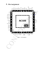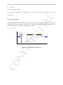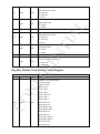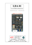
1
TI AL AC100 ID EN User Manual NF Revision 1.0 CO 2014/06/10 Copyright©2014 X-Powers Technology. All Rights Reserved. Declaration TI AL This documentation is the original work and copyrighted property of X-Powers. Reproduction in whole or in part must obtain the written approval of X-Powers and give clear acknowledgement to the copyright owner. The information furnished by X-Powers is believed to be accurate and reliable. X-Powers reserves the right to make changes in circuit design and/or specifications at any time without notice. X-Powers does not assume any responsibility and liability for its use. Nor for any infringements of patents or other rights of the third parties which may result from its use. No license is granted by implication or otherwise under any patent or patent rights of Allwinner. This documentation neither states nor implies warranty of any kind, including fitness for any particular application. CO NF ID EN Third party licences may be required to implement the solution/product. Customers shall be solely responsible to obtain all appropriately required third party licences. X-Powers shall not be liable for any licence fee or royalty due in respect of any required third party licence. X-Powers shall have no warranty, indemnity or other obligations with respect to matters covered under any required third party licence. About Documentation TI AL This documentation of AC100 is intended to be used by board-level product designers and product software developers. The manual assumes that the reader has a background in computer engineering and/or software engineering and understands concepts of digital system design, microprocessor architecture, Input / Output (I/O) devices, industry standard communication and device interface protocols. Organization CO NF ID EN This document aims to describe the AC100 from following aspects: block diagram, pin assignment, pin/signal description, electrical characteristics, typical application, system description and register description. Revision History Date Description V0.1 2014/3/3 Complete Draft V0.2 2014/5/14 Modify the format V1.0 2014/6/10 Modify the format CO NF ID EN TI AL Version Table of Contents Declaration ...................................................................................................................................................... 2 TI AL About Documentation ..................................................................................................................................... 3 Revision History.............................................................................................................................................. 4 Table of Contents ............................................................................................................................................ 5 1. Description .................................................................................................................................................. 8 2. Features ....................................................................................................................................................... 9 3. Applications .............................................................................................................................................. 10 EN 4. Functional Block Diagram ........................................................................................................................ 10 4.1. Functional Block Diagram ............................................................................................................. 10 4.2. Data Path Diagram ......................................................................................................................... 11 5. Pin Assignment.......................................................................................................................................... 12 ID 6. Package Dimension ................................................................................................................................... 13 7. Pin/Signal Description............................................................................................................................... 14 8. Electrical Characteristics ........................................................................................................................... 16 NF 8.1. Absolute Maximum Ratings ........................................................................................................... 16 8.2. Recommended Operating Conditions............................................................................................. 16 8.3. Static Characteristics ...................................................................................................................... 17 CO 9. Analog Performance Characteristics ......................................................................................................... 18 10. Typical Power Consumption ................................................................................................................... 20 11. Function Description ............................................................................................................................... 21 11.1. Power ............................................................................................................................................ 21 11.2. Clock ............................................................................................................................................ 22 11.3. PLL ............................................................................................................................................... 24 11.4. TWI/RSB Interface ....................................................................................................................... 25 11.4.1. TWI Interface .................................................................................................................... 25 11.4.2. RSB Interface .................................................................................................................... 26 11.5. I2S/PCM Interface ........................................................................................................................ 28 TI AL 11.6. Stereo ADC................................................................................................................................... 32 11.7. Stereo DAC .................................................................................................................................. 32 11.8. Mixer ............................................................................................................................................ 32 11.8.1. DAC Output Mixers .......................................................................................................... 32 11.8.2. ADC Record Mixers .......................................................................................................... 32 11.8.3. Digital Mixers .................................................................................................................... 33 EN 11.9. Analogue Audio Input Path .......................................................................................................... 34 11.9.1. Microphone Input .............................................................................................................. 34 11.9.2. AXIL/R Input .................................................................................................................... 34 11.9.3. LINEINL/R Input .............................................................................................................. 35 ID 11.10. Analogue Audio Output Path...................................................................................................... 36 11.10.1. Headphone Output ........................................................................................................... 36 NF 11.10.2. Earpiece Output ............................................................................................................... 36 11.10.3. Speaker Output ................................................................................................................ 37 11.10.4. Line Output...................................................................................................................... 37 11.11. Digital Microphone Interface ..................................................................................................... 38 CO 11.12. Audio Jack Detect....................................................................................................................... 39 11.13. Interrupt ...................................................................................................................................... 40 11.14. Digital Audio Process for ADC .................................................................................................. 41 11.14.1. High Pass Filter ............................................................................................................... 42 11.14.2. Auto Gain Control ........................................................................................................... 42 11.15. Digital Audio Process for DAC .................................................................................................. 46 11.15.1. High Pass Filter ............................................................................................................... 47 11.15.2. Dynamic Range Control .................................................................................................. 47 11.16. RTC Module ............................................................................................................................... 50 CO NF ID EN TI AL 12. Register List ............................................................................................................................................ 51 1. Description TI AL The AC100 is a highly integrated audio codec and RTC subsystem designed for tablet and smart mobile application platforms. It has three I2S/PCM interface, 2 channels DAC and 2 channel ADC with a high level of mixed-signal integration. Three audio interface are available in order to provide independent and fully asynchronous connections to multiple processors, typically such as an application processor, baseband and bluetooth transceiver. An integrated digital PLL supports a large range of input/output frequencies, and It can generate required audio clocks for codec from standard audio crystal rate such as 22.5792MHz and 24.576MHz, also can be from common reference clock frequencies such as 12MHz, 13MHz and 19.2MHz, and an internal RC oscillator can be used in Free-running Mode, where the application processor can be inactive during voice call application. The 2 ADC and 2 DAC in device use advanced multi-bit delta-sigma modulation technique to convert data between analog and digital . The SNR performance can reach 100 dB A-wight. EN Five analog input paths allow diverse analog audio sources such as three sets of differential microphone, one differential or single-ended linein and one stereo FM input. One ground-reference headphone output is provided. The output amplifier are powered from an integrated Charge Pump in order to achieve a higher quality, less power consumption in headphone playback, whist without any DC blocking capacitor and avoiding unwanted noise. ID A mono, differential BTL drive amplifier is available for driving the handset receiver. Two stereo differential speaker output is available by using an external amplifier to drive the loud-speaker. It can also be configured as single-ended output pin for some application of external single-ended amplifier. NF The flexible analogue and digital mixers form a varied signal routing to support a complicated application. AC100 is controlled through TWI (2-wire serial interface ) or RSB① (reduced serial bus) . It works only in the slave mode . CO The integrated DRC(Dynamic Range Controller) function in AC100 provide an useful digital sound processing capability in DAC playback path to speaker . It is uesed to attenuate the peak signals and boost the low-level signals by adjusting the output signal gain in some conditions. The DRC functions can be enable or disable in the playback path . The integrated AGC(Automatic Gain Controller) function can be used to maintain a constant recording level in ADC record path . The DRC can make an improvement in background noise by setting a programmable Noise Gate to attenuate very low-level input signals . Note: ① The RSB is independent R&D by x-powers, supports a special protocols with a simplified two wire protocol on a push-pull bus. The transfer speed in AC100 can be up to 10MHz . 2. Features The AC100 features: • 2 ADCs and 2 DACs @ 24-bit and inter PLL processing with flexible clocking scheme TI AL • Up to 100dB SNR during DAC playback path (A ' weight) • Up to 95dB SNR during ADC record path (A ' weight) • Capless stereo headphone driver – Integrated charge pump for 0V reference – 18mW @1.8V • Mono differential earpiece driver – >65 mW/CH (THD+N ≤ -70dB, 16Ohm Load) EN • Two stereo differential speaker outputs using external amplifier to drive the loud speaker • Differential Line output with 1 Vrms full scale output voltage • Five audio inputs ID – Three differential analog microphone inputs with 30dB~48dB boost amplifier gain – One mono differential or single-ended line-in input – One stereo auxiliary input for external accessory connection • Two low noise analog microphone bias • Audio jack insert/ button press detection • TWI/RSB control interface NF • 24-bit 8KHz ~ 192KHz I2S/PCM interface • Support Dynamic Range Controller (DRC) adjusting the DAC playback output • Support Automatic Gain Control (AGC) adjusting the ADC recording output • SRC for synchronisation between audio interface or digital audio data mixing CO • Soft mute circuit for pop noise suppression • Support digital microphone interface • RTC and Three clock output • QFN 68-pin package, 8mm x 8mm 3. Applications • Tablets TI AL • Smart Phone and Music phone AVCC VRP VRA1 VAR2 VRN SRC HBIAS MIC1P MIC1N MIC2P MIC2N ADC_R X32KO X32KI VIO-RTC VCC-RTC SDIN3 SDIN2 SDOUT2 MCLK2 BCLK2 LRCK2 High Filter NF G IRQ-RTC RTC CKO1-RTC CKO2-RTC CKO3-RTC No SRC ADC Volume Input Mixer LDO2 PCM Mono #3 ADC_L CO MIC3P MIC3N LINEINL LINEINR AXIL AXIR Boost I2S/PCM #2 ID MBIAS AVCC HBIAS SDIN1 I2S/PCM #1 Reference Voltage AVCC MBIAS EN LDO1 AGND AVCC SDOUT1 MCLK1 BCLK1 LRCK1 VCC-IO2 VCC-IO1 VDD-CORE Functional Block Diagram LDOIN 4.1. BCLK3 LRCK3 SDOUT3 4. Functional Block Diagram AGC & DRC CPGND Charge Pump CPVDD CPVEE CPP CPN VPP VEE DAC_L MixerL DAC_L DAC_L MixerL DAC_R MixerR DAC Volume HPOUTL HPOUTR Headphone High Filter MixerR DAC_R DAC_R Figure 1 Functional Block Diagram DAC_L MixerL DAC_R MixerR HPOUTFB EAROUTP EAROUTN Earpiece Output Mixer MixerL MixerR Left Speak MixerL MixerR Right Speak MIC1 MIC2 MixerL MixerR SPOLP SPOLN SPORP SPORN LINEOUTP LINEOUTN Lineout 1x CLK L R I2S/PCM Interface L R L R L R I2S/PCM Interface L R L R SDIN3 SDOUT3 LRCK3 BCLK3 SDIN2 SDOUT2 LRCK2 BCLK2 MCLK2 SDIN1 SDOUT1 BCLK1 System Clock Path LRCK1 Data Path Diagram MCLK1 4.2. PCM Interface 1x CLK SYSCLK MCLK2 1x CLK BCLK1 DPLL TI AL MCLK1 L/R Channel Source Exchange L/R Channel Source Exchange 3x CLK Slot0 BCLK2 Slot1 Slot0 SRC1 DAP SRC1 DAP DAP Slot1 DAP DAP DAP + MIC1P + MIC1N G MICBST1 + MIC2N - m m MIC2P G MICBST2 m m MIC3P m MIC3N m G ADCL D A P m LINEINL/N + LINEINR/P - G m m m m AXIL AXIR + - G m G ADCR D A P m DACL D A P DACR m m m m ID G G m G SPKOUT2N SPKOUT1P SPKOUT1N EAROUTP m EAROUTN HPOUTL G MIXL DACR -1 m m -1 HPOUTR G MIXR MICBST1 MICBST2 MIXL MIXR m m m m LINEOUTP + NF m m DACL D A P Figure 2 Data Path Diagram CO MIXL MIXR DACL MIXL DACR MIXR EN m + + m m + + DMIC_DATA SPKOUT2P MIXL MIXR + SRC G LINEOUTN LRCK2 SDOUT2 SDIN2 NC IRQ_AUDIO BCLK3 LRCK3 VCC_IO2 42 41 40 39 38 37 36 35 TI AL BCLK2 43 LRCK1 47 VCC_IO1 BCLK1 48 44 MCLK1 49 SDIN1 MCLK2 46 SDOUT1 SDA 50 45 16 17 AVCC SPORP 18 SPORN EAROUTN 68 Figure 3 Pin Assignment CO 19 SPOLP 15 AXIL 14 67 EAROUTP AXIR 20 SPOLN 13 66 AGND MIC3N 21 VRA2 12 65 22 VRA1 VRN 64 NF MIC3P MBIAS 23 VPP 11 63 24 VEE LINEOUTR LDOIN EN 62 10 VDD_CORE 25 HPOUTL LINEOUTL 61 26 HPOUTFB 9 X32KO AC100 VRP 60 8 X32KI 27 HPOUTR LINEINL 59 7 VIO_RTC 28 CPVEE LINEINR 58 ID VCC_RTC 29 CPN 6 57 HBIAS CKO3_RTC 30 NC 5 56 MIC2N CKO2_RTC 31 CPP 4 55 MIC2P CKO1_RTC 32 CPVDD 3 54 MIC1N IRQ_RTC 33 SDIN3 MIC1P 53 2 SCK 34 SDOUT3 1 52 NC NC 51 5. Pin Assignment EN TI AL 6. Package Dimension CO NF ID Figure 4 Package Dimension 7. Pin/Signal Description TI AL This chapter describes the 68 pins of AC100 from four aspects: pin number, signal name, type, and pin definition. All the pins are classified into four groups, including digital IO pin, analog IO pin, filter/reference, and power/ground. There are five pin types here: O for output, I for input, I/O for input/output, P for power, and G for ground. Pin Number Signal Name Type Description 49 MCLK1 I I2S interface master input clock 1 45 SDIN1 I First I2S interface serial data input 46 SDOUT1 O First I2S interface serial data output 48 BCLK1 I/O First I2S interface serial bit clock 47 LRCK1 I/O First I2S interface synchronous clock 50 MCLK2 I I2S interface master iuput clock 2 40 SDIN2 I 41 SDOUT2 O Second I2S interface serial data output 43 BCLK2 I/O Second I2S interface serial bit clock 42 LRCK2 I/O Second I2S interface synchronous clock 33 SDIN3 I Third I2S interface serial data input 34 SDOUT3 O Third I2S interface serial data output 37 BCLK3 I/O Third I2S interface serial bit clock 36 LRCK3 I/O Third I2S interface synchronous clock 51 SDA I/O TWI interface serial data(Open-drain) RSB interface serial data 53 SCK I TWI interface serial clock input RSB interface serial clock input NF ID Second I2S interface serial data input IRQ_AUDIO O IRQ for accessory insert and button detect(Open-drain) IRQ_RTC O IRQ for RTC alarm interrupt…(Open-drain) X32KI I The external oscillator input singal X32KO O The external oscillator output singal CKO1_RTC O RTC 32.768 KHz clock output(Push-pull ) CO 38 EN Digital IO Pins CKO2_RTC O RTC 32.768 KHz clock output(Open-drain) CKO3_RTC O RTC 32.768 KHz clock output(Open-drain) 2 MIC1P I Positive differential input for MIC1 3 MIC1N I Negative differential input for MIC1 4 MIC2P I Positive differential input for MIC2 5 MIC2N I Negative differential input for MIC2 64 MIC3P/ DMICCLK I O Analog Positive differential input for MIC3 Digital microphone clock output 66 MIC3N/ DMICDAT I O Negative differential input for MIC3 Digital microphone data input 8 LINEINL I Left single-end or differential input for LINE-IN 54 60 61 55 56 57 Analog IO Pin LINEINR I Right single-end or differential input for LINE-IN 68 AXIL I Auxiliary left Channel input 67 AXIR I Auxiliary right Channel input 25 HPOUTL O Headphone amplifier left channel output 27 HPOUTR O Headphone amplifier right channel output 19 SPOLP O Differential positive output to speaker1 amplifier 20 SPOLN O Differential negative output to speaker1 amplifier 17 SPORP O Differential positive output to speaker2 amplifier 18 SPORN O Differential negative output to speaker2 amplifier 14 EAROUTP O Earpiece amplifier positive differential output 15 EAROUTN O Earpiece amplifier negative differential output 11 LINEOUTP O Positive output for LINE-OUT 10 LINEOUTN O Negative output for LINE-OUT Filter/Reference TI AL 7 MBIAS O First bias voltage output for main microphone 6 HBIAS O Second bias voltage output for headset microphone 26 HPOUTFB I Pseudo differential headphone ground reference 29 CPN I/O Charge pump flying-back capacitor 31 CPP I/O Charge pump flying-back capacitor 22 VRA1 O Internal reference voltage 21 VRA2 O Internal reference voltage 9 VRP O Internal reference voltage 12 VRN O Internal reference voltage 16 AVCC P Analog power 13 AGND 32 ID Power/Ground EN 65 Analog ground CPVDD P Analog power for headphone charge pump 28 CPVEE P Charge pump negative decoupling Pin 23 VPP P Headphone PA positive voltage input 24 VEE P Headphone PA negative voltage input VDD_CORE P Digital power for digital core VCC_IO1 P Digital power for digital I/O buffer(I2S1&I2S2) VCC_IO2 P Digital power for digital I/O buffer(I2S3) LDOIN P Input power for Audio_LDO VIO_RTC P Digital power for RTC VCC_RTC P Input power for RTC_LDO GND G Digital ground NC -- Not connected 62 44 35 63 59 CO 58 NF G 69 Others 1,30,39,52 8. Electrical Characteristics 8.1. Absolute Maximum Ratings Parameter MIN MAX Unit LDO_IN LDO Input power for AudioCODEC -0.3 3.63 V VDD_CORE Digital power for Audio digital core, it can be generate by inner LDO -0.3 1.32 V VCC_IO1 Digital power for digital I/O buffer (I2S1&I2S2) -0.3 3.63 V VCC_IO2 Digital power for digital I/O buffer (I2S1&I2S3) -0.3 3.63 V CPVDD Analog power for headphone charge pump -0.3 2.0 V VCC_RTC LDO Input power for RTC -0.3 3.63 V VIO_RTC Digital power for RTC digital core, it can be generate by inner LDO -0.3 1.32 V TA Operating Ambient Temperature -20 85 ℃ VESD ESD 4 -- KV 8.2. EN Symbol TI AL Absolute maximum ratings are stress ratings only. Permanent damage to the device may be caused by continuously operating at or beyond these limits. Device functional operating limits and guaranteed performance specifications are given under electrical characteristics at the test conditions specified. Recommended Operating Conditions Description MIN TPY MAX Unit LDO_IN LDO Input power for AudioCODEC 1.35 1.8/1.5 3.63 V VDD_CORE Digital power for Audio digital core, it can be generate by inner 1.08 1.2 1.32 V -- 1.8/3.3 3.63 V Digital power for digital I/O buffer (I2S1&I2S3) -- 1.8/3.3 3.63 V Analog power for headphone charge pump 1.2 1.8 1.98 V VCC_RTC LDO Input power for RTC 1.35 1.8/3.3 3.63 V VIO_RTC Digital power for RTC digital core, it can be generate by inner 1.08 1.2 1.32 V -- 0 -- V LDO VCC_IO2 CPVDD Digital power for digital I/O buffer (I2S1&I2S2) NF VCC_IO1 ID Parameter LDO Ground reference CO GND,AGND 8.3. Static Characteristics Symbol Parameter Test condition Min Typical VIN Input Voltage Range -- -0.3 -- VIH High Level Input Voltage VOL V VCCIO2+0.3 2.4 -- V VCCIO=1.8V 1.4 -- 1.98 VCCIO=3.0v -0.3 -- 0.7 VCCIO=1.8V -0.3 -- 0.7 VCCIO=3.0v 2.7 -- NA VCCIO=1.8V 1.5 -- NA VCCIO=3.0v NA -- 0.4 VCCIO=1.8V NA -- 0.4 TBD TBD TBD uA NA NA 5 pF NA NA 5 pF Low Level Input Voltage V High Level Input Voltage V Low Level Input Voltage V Tri-state Output Leakage Current -- C IN Input Capacitance -- C OUT Output Capacitance -- NF ID EN I OZ CO 3.6 TI AL VOH Units VCCIO1+0.3 VCCIO=3.0v VIL Max 9. Analog Performance Characteristics PARAMETER Performance MIN TYP MAX UINT DAC to Headphone on HPOUTL or HPOUTR(R=10kΩ) FScale Output Level 0dB 1KHz 0.9 Vrms SNR(A-weighted) 0dB 1KHz 100 dB THD+N(NO-Aweight) 0dB 1KHz -84 dB Crosstalk(L/R) 0dB 1KHz -88/-88 dB TI AL DAC Output Path TEST CONDITIONS DAC to Headphone on HPOUTL or HPOUTR(R=16Ω) 0dB 1KHz 0.5 Vrms SNR(A-weighted) 0dB 1KHz 99 dB THD+N(P0=15mW) 0dB 1KHz -81 dB THD+N(P0=5mW) 0dB 1KHz -82 dB Crosstalk(L/R) 0dB 1KHz EN FScale Output Level -82/-82 dB DAC to Headphone on HPOUTL or HPOUTR(R=32Ω) FScale Output Level SNR(A-weighted) THD+N(P0=15mW) 0.7 Vrms 0dB 1KHz 100 dB 0dB 1KHz -83 dB 0dB 1KHz -83 dB -86/-86 dB ID THD+N(P0=5mW) 0dB 1KHz Crosstalk(L/R) 0dB 1KHz DAC to Earpiece Driver on EAROUTP and EAROUTN(R=16Ω) 0dB 1KHz 1.0 Vrms SNR(A-weighted) 0dB 1KHz 100 dB THD+N(P0=12mW) 0dB 1KHz -81 dB DC Offset at load 0dB 1KHz 2 mV NF FScale Output Level DAC to SPK signal on SPKOUTLP and SPKOUTLN(R=10KΩ) 0dB 1KHz 1.8 Vrms SNR(A-weighted) 0dB 1KHz 102 dB THD+N 0dB 1KHz -82 dB 0dB 1KHz 0.7 mV CO FScale Output Level DC Offset at load DAC to LINEOUT signal on LINEOUTP and LINEOUTN(R=10KΩ) ADC Input Path Performance FScale Output Level 0dB 1KHz 0.9 Vrms SNR(A-weighted) 0dB 1KHz 98 dB THD+N 0dB 1KHz -81 dB DC Offset at load 0dB 1KHz 0.5 mV FScale Input Level 0dB Gain 1KHz 0.5 Vrms SNR(A-weighted) -1dB 1KHz, 0dB Gain 96 dB MIC1 /2/3to ADC via ADC mixer -1dB 1KHz, 0dB Gain -85 dB SNR(A-weighted) 30mV,1KHz, 30dB Gain 81 dB THD+N 30mV,1KHz, 30dB Gain -76 dB SNR(A-weighted) 30mV,1KHz, 39dB Gain 81 dB THD+N 30mV,1KHz, 39dB Gain -76 dB SNR(A-weighted) 10mV,1KHz, 48dB Gain 73 dB THD+N 10mV,1KHz, 48dB Gain -72 dB FScale Input Level 0dB 1KHz 0.9 Vrms SNR(A-weighted) 1KHz 93 dB THD+N 1KHz -85 dB Crosstalk(L/R) 1KHz -85/-85 dB FScale Input Level 0dB 1KHz 0.9 Vrms SNR(A-weighted) 1KHz 92 dB THD+N 1KHz -82 dB Crosstalk(L/R) 1KHz -88/-88 dB 0dB Gain 1KHz 0.5 Vrms -1dB 1KHz, 0dB Gain 98 dB -1dB 1KHz, 0dB Gain -91 dB 30mV,1KHz, 30dB Gain 83 dB 30mV,1KHz, 30dB Gain -78 dB TI AL THD+N LINEIN to ADC via ADC mixer Bypass Path Performance EN AXIIN to ADC via ADC mixer MIC1/2/3 to Headphone via output mixer FScale Input Level SNR(A-weighted) THD+N SNR(A-weighted) ID THD+N SNR(A-weighted) 30mV,1KHz, 39dB Gain 83 dB THD+N 30mV,1KHz, 39dB Gain -79 dB SNR(A-weighted) 10mV,1KHz, 48dB Gain 74 dB THD+N 10mV,1KHz, 48dB Gain -73 dB NF LINEIN to Headphone via output mixer FScale Input Level 0dB 1KHz 1 Vrms SNR(A-weighted) -1dB 1KHz 98 dB THD+N(-1dBFS) -1dB 1KHz -92 dB Crosstalk(L/R) -1dB 1KHz -89/-89 dB FScale Input Level 0dB 1KHz 1 Vrms SNR(A-weighted) -1dB 1KHz 102 dB THD+N(-1dBFS) -1dB 1KHz -93 dB Crosstalk(L/R) -1dB 1KHz -88/-88 dB CO AXIIN to Headphone via output mixer 10. Typical Power Consumption Default Test Conditions: OPERATING TEST CONDITIONS LDOIN LDOIN,VCC-RTC supplies, 1.8V MODE RTC only LDO enabled 32.768KHz clock, XTAL enabled 0uA three output enable Standby All supplies present, 1.8V LDO enabled XTAL enabled Default register settings Music Playback to Headphone(32Ω load) fs=44.1KHz, AIF1 to DAC to AVCC VCC-IO1 VCC-IO2 CPVDD VCC-RTC 3V 1.8V 3V 1.8V 3V 0uA 0uA 0uA 0uA 12uA 3V 1.8V 3V 1.8V 3V EN No clocks supply, TI AL LDOIN=CPVDD=1.5V,AVCC=3.0V,VCC-IO1=VCC-IO2=1.8V,VCC-RTC=3.0V 73uA 62uA 0uA 0uA 0uA 12uA 1.8V 3V 1.8V 3V 1.8V 3V 1.5mA 4.1mA 0.013mA 0mA 2.4mA 12uA 1.8V 3V 1.8V 3V 1.8V 3V 1.4mA 4.5mA 0.023mA 0mA 0mA 12uA 1.8V 3V 1.8V 3V 1.8V 3V 0.75mA 4.1mA 0mA 0mA 2.0mA 12uA SYSCLK=MCLK=24.576MHz, HPOUT(stereo) Voice record to AIF1 ID 24bit I2S,Slave mode fs=44.1KHz, MIC1 to ADC to SYSCLK=MCLK=24.576MHz, NF AIF1(mono) 24bit I2S,Slave mode Analog-Analog Voice Path (eg. Analog Voice call) fs=8 kHz, Linein to Hp, SYSCLK=MCLK=24.576MHz CO Mic1 to Lineout, 11. Function Description 11.1. Power TI AL There are a Power-Reset circuit in AC100 uesed to reset all the circuit and register to a standby state after power up. The Power-Reset circuit make all the supply power need no specific timing. All the supply voltages are illustrated in the below figure. AC100 POWER DOMAIN LDOIN 1.5~~3.3 V VCC_RTC RTC_VCC RTC IO Buffer POR RTCBG VDD_CORE 1.2 V VIO_RTC RTC_LDO RTC Digital/ I2C/RSB/ 32KHz/ Register Part 1 LS LS AVCC 3.0 V REG LS CPVDD 1.8 V VCC_IO1/VCC_IO2 VCC_IO1/VCC_IO2 LDOIN VDD_CORE AUDIO_LDO Audio Digital/ I2S/DLL/ HMIC Detect/ Register Part 2 EN 1.8~~3.3 V LS I2S1/I2S2/I2S3 Digital IO VCC_RTC LS CPVDD LS Charge Pump LS 1.8~~3.3 V VIO_RTC LS 1.2V LS DETECT AVCC Three power status (1)All off (2)RTC_VCC/VIO_RTC power on,Other powers off (3)All on ID Audio Analog/ Audio BG/ MICBIAS/ HMICBIAS Figure 5 Power Management NF VDD-CORE is 1.2V for audio digital core power generated from LODIN pin, which also can be direct supplied from VDD-CORE pin. VDD-IO1 is digital I/O power for I2S1 and I2S2. VDD-IO2 is digital I/O power for I2S3. AVCC is for analog power. CPVDD for charge pump power. VIO-RTC is RTC digital core power generated from VCC-RTC. CO When the AC100 is not working, it need to set the supply properly to prevent power leakage. There are two settings to select. It's best to power off all the supply. The other is to make sure AVCC and CPVDD both power on. At the setting below, AC100 has the best performance. LDOIN VDD_CORE AVCC CPVDD VCC-IO1 VCC-IO2 VCC_RTC VIO_RTC 1.5~~3.3 V 1.2 V 3V 1.8 V 1.8/3.3 V 1.8/3.3 V 1.8/3.3 V 1.2 V Supplied N/A Supplied Supplied Supplied Supplied Supplied N/A * VDD_CORE and VIO_RTC generated by internal LDO. 11.2. Clock The system clock(SYSCLK) of AC100 must be 512*fs(fs=48KHz or 44.1KHz). So the system should arrange the divider to generate 24.576MHz for audio clock series of 48KHz or 22.5792MHz for series of 44.1KHz. TI AL SYSCLK can be selected from I2S1CLK or I2S2CLK which derived from MCLK1, MCLK2 or PLL. MCLK1 and MCLK2 are always provided externally while the PLL reference clock can be select from MCLK1, MCLK2, BCLK1, BCLK2. I2S1CLK is the reference of the first I2S clocking zone. I2S2CLK is the reference of the second I2S clocking zone. The third I2S only support master mode. Its clocking zone must be synchronized with either of the I2SnCLK(n=1,2). In master mode, LRCK and BCLK are derived internally from I2SnCLK. In slave mode, LRCK and SCLK are supplied externally and BCLK can be used as the PLL input reference. EN SYSCLK is the reference of ADC, DAC, DVC, MIXER, AGC and DRC module. If SRC1 or SRC2 is used, SYSCLK must be set by PLL, then the SRCnCLK is auto provided for SRC module. If all the relevant module above is not used, the SYSCLK needn't be configured. CO NF ID There are also an internal Oscillator to generate a clock signal for direct-path mode. In this mode, the oscillator supply clock to charge pump, adjustment circuit, headphone detect circuite.g... In direct-path case, no external clock need . AC100 CLOCK SYSTEM SRC1CLK SRC1 SRC2CLK SRC2 ADCCLK TI AL ADC_DIGITAL DACCLK DAC_DIGITAL AGCCLK HPF & AGC DRCCLK HPF & DRC MCLK2 BCLK1 M U X DPLL M U X I2S1CLK M U X I2S2CLK ACLK1 DVCCLK DVC/MIXER AIF1_BCLK/LRCK_CTL BCLK2 M U X EN MCLK1 SYSCLK ACLK2 AIF2_BCLK/LRCK_CTL ACLK3 AIF3_BCLK/LRCK_CTL ID M U X BCLK1A M U X BCLK2A AIF1_TX/RX AIF2_TX/RX BCLK3A M U X AIF3_TX/RX ADDA CK4M M U X REGISTER PART 2/ HMICBIAS DETECT TWI/RSB RTC OSC SCK X32KI NF WCLK REGISTER PART 1 CO Figure 6 Clocking Management CK32K RTC/ CK32K OUTPUT 11.3. PLL TI AL A Phase-Locked Loop(PLL) is used to provide a flexible input clock range from 128KHz to 24MHz. The source of the PLL can be set to MCLK1, MCLK2, BCLK1 or BCLK2 by setting register. The PLL output is always used to provide the system clock(SYSCLK) of AUDIO codec when 24.576MHz or 22.5792MHz can not be provided from MCLK. The PLL transmit formula as below: FOUT =(FIN * N) / (M * (2K+1)) ; (N= N_i + 0.2*N_f) Table 1 clock setting for SYSCLK=24.576 MHz M N K FOUT 128K 1 576 1 24.576M 192K 1 384 1 24.576M 256K 1 288 1 24.576M 384K 1 ... .... 25 42 19.2M 25 192 1 24.576M ... 1 24.576M 307.2 1 24.576M 238.2 1 24.576M 96 1 24.576M ID 6M 13M EN FIN Table 2 clock setting for SYSCLK=22.5792 MHz FIN 1 N K FOUT 529.2 1 22.5792M 192K 1 352.8 1 22.5792M 256K 1 264.6 1 22.5792M 384K 1 176.4 1 22.5792M NF 128K M .... ... 1 22.5792M 38 429 1 22.5789M 13M 19 99 1 22.5789M 19.2M 25 88.2 1 22.5792M CO ... 6M 11.4. TWI/RSB Interface AC100 can support two series control interface protocol for writing to or readback from registers on SCK and SDA pins . One is TWI interface, the other is RSB interface. RSB is top-priority for higher efficiency and lower power consumption. TI AL 11.4.1. TWI Interface TWI is a 2-wire (SCK/SDA) half-duplex serial communication interface, supporting only slave mode. SCK is used for clock and SDA is for data. SCK clock supports up to 400 KHz rate and SDA data is a open drain structure. SDA SCK 1-7 8 9 1-7 8 9 ID S EN A master controller initiates the transmission by sending a “start” signal, which is defined as a high-to-low transition at SDA while SCK is high. The first byte transferred is the slave address. It is a 7-bit chip address followed by a R/W bit. The chip address must be 0011010x. The R/W bit indicates the slave data transfer direction. Once an acknowledge bit is received, the data transfer starts to proceed on a byte-by-byte basis in the direction specified by the R/W bit. The master can terminate the communication by generating a “stop” signal, which is defined as a low-to-high transition at SDA while SCK is high. START ADDRESS R/W ACK DATA 1-7 ACK 8 9 P DATA ACK STOP Figure 7 TWI Interface NF The formats of “write” and “read” instructions are shown in below. 1 s 1 1 1 Wr A 1 1 Wr A 8 Register Address CO s 7 Device Address 7 Device Address S: start Condition Slave Address: 7-bit Device Address Wr: 0 for Write Command Rd: 1 for Read Command 1 A Write Word Protocol 8 Register Address 1 S 1 A 8 Data Byte High Read Word Protocol 8 1 1 Rd A Device Address 1 A 8 Data Byte High A: 0 for ACK, 1for NACK Data Byte: 16-bit Mixer data : Master-to-Slave : Slave-to-Master Command Code: 8-bit Register Address Figure 8 TWI Read and Write 1 P 1 A 8 Data Byte Low 1 A 1 P 11.4.2. RSB Interface RSB interface supports a special protocols with a simplified two wire protocol on a push-pull bus. So the transfer speed can be up to 10MHz and the performance will be improved much. AC100 works only in slave mode. Master TI AL RSB support multi-slaves. It uses CK as clock and uses CD to transmit command and data.the Bus Topology is showed below: CK CD Slave1 Slave2 Slave3 EN Figure 9 RSB Bus Topology The start bit marks the beginning of a transaction with the slave device.When CK is high, a change from high to low on CD is defined as a start condition. This start condition notifies the selected device to start a transfer. ID CK CD S NF Figure 10 Start signal RSB protocol uses parity bit to check the correction of every byte,The checked object is the 7, 8 or 15 bit in front of the parity bit. CO 7 6 5 4 3 2 1 0 C Figure 11 Parity bit ACK bit is the acknowledgement from device to host, The ACK is active low. When device finds the parity bit is error, it will not send ACK to host, so host can know that an error happens in the transaction. Set run-time slave address(RTSADDR) command. It is used to set run time slave address(RTSADDR) for different devices in the same system. There are 15 devices in a system at most. The RTSADDR can be selected from the command code set and a device 's RTSADDR can be modified many times by using set run-time slave address command. 1 7 1 15 1 7 1 2 1 2 S 0x74 C SADDR C RTSADDR C HD A DH HOST Device Figure 12 RTSADDR command 1 7 1 7 1 8 1 2 S 0x45,0x4E,0x53 C RTSADDR C DADDR C HD TI AL Read command is used to read data from device.It has byte,half word and word operation.When devices receives the command,they shall check if the command's RTSADDR matches their own RTSADDR.The device's RTSADDR is setted by set run-time slave address(RTSADDR) command. 8 1 DATA0 C ... 8 1 2 DATA n C DH HOST Device len = 1,2,4 Figure 13 Read command 1 7 1 7 1 S 0x27,0x2c,0x31 C RTSADDR C EN Write command is used to write data to the devices.It has byte,half word and word operation.When devices receive the command,they shall check if the command's RTSADDR matches their own RTSADDR.The device's RTSADDR is setted by set run-time slave address(RTSADDR) command. 8 1 8 1 DADDR C DATA0 C ... len = 1,2,4 CO NF ID Figure 14 Write command 8 1 2 1 2 DATA n C HD A DH HOST Device 11.5. I2S/PCM Interface TI AL There are three I2S/PCM interfaces which can be configured as master mode or slave mode in AC100. The three I2S/PCM interfaces provide flexible connectivity with multiple processors (e.g. Application processor, Baseband processor and Wireless transceiver ). Interface I2S1 and I2S2 can be configured as Master or Slave, the third interface I2S3 operates in Master mode and supports PCM mode only. In the general case, the digital audio interface uses four pins as below: BCLK: Bit clock for data synchronization LRCK: Left/Right data alignment clock SDOUT: output data for ADC data SDIN: input data for DAC data I2S mode Left justified mode Right justified mode PCM short mode ID EN I2S1 and I2S2 audio interface support four different data formats as below. But I2S3 supports PCM short mode only. On the first digital audio interface I2S1, TDM is available for all four farmart and AC100 can use it to transmit or receive up to four channel data on timeslot0 and timeslot1 simultaneously. LRCK_DIV Left channel NF BCLK Right channel LRCK SDIN/ SDOUT 1 2 MSB n LSB CO WORD_SIZE 1 2 MSB WORD_SIZE I2S Justified mode Figure 15 n LSB I2S Justified mode LRCK_DIV BCLK Left channel Right channel LRCK 1 2 MSB n LSB 1 2 MSB n LSB TI AL SDIN/ SDOUT WORD_SIZE WORD_SIZE Left Justified mode Figure 16 Left Justified mode LRCK_DIV BCLK Left channel EN LRCK Right channel SDIN/ SDOUT 1 2 MSB n LSB 1 2 MSB WORD_SIZE n LSB WORD_SIZE ID Right Justified mode Figure 17 Right Justified mode LRCK_DIV NF Short Short BCLK LRCK SDIN/ SDOUT Left channel 1 2 MSB WORD_SIZE CO Right channel n 1 2 LSB MSB n LSB WORD_SIZE Pcm mode A(BCLK_INV=0) Figure 18 Pcm mode A(LRCK_INV=0) LRCK_DIV Short Short BCLK LRCK Left channel Right channel n 1 2 LSB MSB 1 2 MSB n LSB TI AL SDIN/ SDOUT WORD_SIZE WORD_SIZE Pcm mode B(BCLK_INV=1) Figure 19 Pcm mode B(LRCK_INV=1) LRCK_DIV Short Short LRCK EN BCLK Left channel SDIN/ SDOUT 1 2 MSB Right channel n 1 2 LSB MSB WORD_SIZE n LSB WORD_SIZE ID Pcm mode A(BCLK_INV=0) NF Figure 20 Pcm mode A mono(LRCK_INV=0) LRCK_DIV Short Short BCLK LRCK Left channel 1 2 MSB CO SDIN/ SDOUT Right channel n 1 2 LSB MSB WORD_SIZE n LSB WORD_SIZE Pcm mode B(BCLK_INV=1) Figure 21 Pcm mode B mono(LRCK_INV=1) LRCK_DIV BCLK Left channel Right channel LRCK SDIN/ SDOUT SLOT0 Left channel SLOT1 Left channel 1 MSB 2 n LSB WORD_SIZE SLOT_SIZE 1 2 SLOT0 Right channel SLOT1 Right channel n 1 LSB WORD_SIZE SLOT_SIZE MSB MSB 2 n 1 LSB WORD_SIZE SLOT_SIZE MSB 2 TI AL I2S TDM mode Figure 22 I2S TDM mode LRCK_DIV BCLK LRCK SDIN/ SDOUT SLOT0 Left channel SLOT1 Left channelSLOT0 Right channel SLOT1 Right channel 1 MSB 2 n LSB WORD_SIZE SLOT_SIZE 1 MSB 2 n 1 LSB WORD_SIZE SLOT_SIZE 2 n LSB MSB WORD_SIZE SLOT_SIZE 1 MSB 2 EN NF ID Figure 23 PCM TDM mode n LSB WORD_SIZE SLOT_SIZE PCM TDM mode CO n LSB WORD_SIZE SLOT_SIZE 11.6. Stereo ADC TI AL The stereo ADC is used for recording stereo sound. The sample rate of the stereo ADC can not be independent of DAC sample rate. In other words, the stereo ADC and DAC must work at a same sample rate. The sample rate is configured by the register ADDA_FS_I2S1 or ADDA_FS_I2S2 depending on which I2SnCLK selected as the system clock(SYSCLK). In order to save power, the left and right analog ADC part can be enabled/disabled separately by setting register ADC_APC_CTRL Bit15 & Bit11. The digital ADC part can be enabled/ disabled by ADC_DIG_CTRL Bit15. The volume control of the stereo ADC is set via register ADC_APC_CTRL Bit14:12 & ADC_APC_CTRL Bit10:8. 11.7. Stereo DAC EN The stereo DAC sample rate is the same as the stereo ADC. The sample rate is configured by the register ADDA_FS_I2S1 or ADDA_FS_I2S2 depending on which I2SnCLK selected as the system clock(SYSCLK). 11.8. Mixer ID In order to save power, the left and right DAC can be enabled/disabled separately by setting register OMIXER_DACA_CTRL Bit15:14. The digital DAC part can be enabled/ disabled by DAC_DIG_CTRL Bit15. The Codec supports three series of mixers for all function requirements: 2 channels DAC Output mixers 2 channels ADC Record mixers Digital mixers NF 11.8.1. DAC Output Mixers CO The output mixer is used to drive analogut output, including headphone, earpiece, speaker,lineout. The following signals can be mixed into the output mixer: LINEINL/R AXIL/R MIC1P/N,MIC2P/N Stereo DAC output 11.8.2. ADC Record Mixers The ADC record mixer is used to mix analog signals as input to the Stereo ADC for recording. The following signals can be mixed into the output mixer: LINEINL/R AXIL/R MIC1P/N,MIC2P/N Stereo DAC output 11.8.3. Digital Mixers TI AL The digital mixers are provided for digital audio data mixing on four I2S1 output paths, two I2S2 output paths and two paths to the stereo DAC. It's separately controlled by the register I2S1_MXR_SRC, I2S2_MXR_SRC and DAC_MXR_SRC. DATA PATH BLOCK DIAGRAM DMICL ADCL ADCL HPF ADCL I2S1_DA0L I2S1_DA1L I2S2_DA0L AGC HPF DMICR ADCR ADCR ADCR DACR DACR HPF AGC DRC HPF DRC DRC HPF HPF I2S2_DA0R I2S1_DA1R I2S1_DA1L I2S1_DA0R I2S1_DA0L HPF AGC I2S2_DA0L EN ADCL I2S1_DA0L I2S1_DA1L I2S2_DA0R ADCR I2S2_DA0R ADCL I2S2_DA0L ADCR I2S2_DA0L I2S2_DA0R I2S1_DA0R ADCL I2S2_DA0L I2S2_DA0R I2S1_DA0L DACL DRC ADCR I2S1_DA0R I2S1_DA1R I2S2_DA0R Volume Control DACL ADCR I2S1_DA0R I2S1_DA1R I2S2_DA0L ADCL AGC HPF ADCL ADCR I2S1/PCM1 I2S3_DAC I2S1_DACR ADC BCLK2 BCLK1 LRCK2 LRCK1 BCLK3 LRCK3 SDIN3 SDOUT3 Figure 24 Digital Data Path DAC PCM3 SDIN2 LRCK2 BCLK2 SDIN1 SDOUT1 LRCK1 BCLK1 CO DACL DACR I2S2/PCM2 SDOUT2 NF DA0L DA0R DA1L DA1R I2S1_DACL I2S2_ADCL Left / Rigth source select / Mono Mix control Left / Rigth source select / Mono Mix control AD0L AD0R AD1L AD1R I2S2_ADCR SRC I2S1_DACR1 I2S1_DACL1 I2S1_DACR0 I2S1_DACL0 I2S1_ADCR1 I2S1_ADCL1 I2S1_ADCR0 I2S1_ADCL0 ID AGC 11.9. Analogue Audio Input Path The Codec supports five Analogue Audio Input paths: LINEINL/R AXIL/R MIC1P/N,MIC2P/N,MIC3P/N TI AL 11.9.1. Microphone Input EN MICIN1P/N, MICIN2P/N, MIC3INP/N provide differential input that can be mixed into the ADC record mixer, or DAC output mixer. MICIN is high impedance, low capacitance input suitable for connection to a wide range of differential microphones of different dynamics and sensitive. There are only two microphone pre-amplifiers for the 3 differential microphone inputs. MICIN1P/N are input to the first pre-amplifier, MICIN2P/N & MICIN3P/N are selected to input the 2nd pre-amplifier by the register ADC_SRCBST_CTRL bit7. Each microphone preamplifier has a separate enable bit, ADC_SRCBST_CTRL Bit15 & Bit11. The gain for each pre-amplifer can be set independently using MIC1BOOST, MIC2BOOST. MBIAS provide reference voltage for electret condenser type(ECM) microphones. MICBIAS MICXP ID MICXN NF Figure 4 Suggested External Microphone Input Drawing Figure 25 Suggested External Microphone Input 11.9.2. AXIL/R Input CO Auxiliary inputs AXIL and AXIR provide 2-channel stereo single-ended input that can be mixed into the DAC output mixer and ADC record mixer. The inputs are high impedance and low capacitance, thus ideally suited to receiving line level signals from external audio equipment or audio FM module . Both auxiliary inputs include programmable volume level adjustments and ADC input mute. The scheme is illustrated below. Passive RF and active Anti_Alias filters are also incorporated within the auxiliary inputs. These prevent high frequencies aliasing into the audio band , otherwise degrading performance. The gain between the AXI inputs and the ADC is logarithmically adjustable from -9dB to 12dB in 1.5dB step by the register AXI_PREG set. The ADC Full Scale input is 1.0Vrms at AVCC =3.0volts. Any voltage greater than full scale will possibly overload the ADC and cause distortion. Note that the full scale input tracks directly with AVCC. + VMID - TI AL Figure 2 AXI input Schematic Figure 26 AXI Input Schematic 11.9.3. LINEINL/R Input LINEINL/R provide one-channel mono differential input or stereo single-ended input that can be mixed into the ADC record mixer or the stereo output mixer. The inputs are suited to receiving line level signals such as external audio equipment or baseband module . CO NF ID EN When the linein input is set as differential signal input LINEINL-LININR to the ADC or to DAC mixer, the linein gain is logarithmically adjustable from -9dB to 12dB in 1.5dB step by the register LINEIN_DIFF_PREG set. 11.10. Analogue Audio Output Path The Codec supports five Analogue Audio Output paths: HPOUTL/R, HPOUTFB SPOLP/N SPORP/N EAROUTP/N LINEOUTP/N TI AL 11.10.1. Headphone Output HPOUTL/R provides two-channel single-ended output to headphone driver. The HPOUTL/R PA input source can be selected from output mixer or directly from DAC by register HPOUT_CTRL Bit15 & Bit14 set. It also can be muted by register HPOUT_CTRL Bit13 & Bit12 set. The headphone PA power up or down by register HPOUT_CTRL Bit11 set. EN HPOUTL/R can drive a 16R or 32R headphone load without DC capacitors by using Charge Pump to generate the negative rails. HPOUTFB is the ground loop noise rejection feedback. HBIAS provides reference voltage for electret condenser type(ECM) microphones. Audio jack insert/ button press detection function is also provided through measuring the HBIAS current. ID HPOUTL HPOUTR NF HBFB Figure 27 Suggested Headphone Output Application HPOUTL/R volumes can be independently adjusted under software control using the HP_VOL[5:0] of the headphone output control registers. The adjustment is logarithmic with an 64dB rang in 1dB step from 0dB to -62dB. The headphone outputs can be muted by writing codes 0x0 to HP_VOL[5:0] bits. CO There are a DC offset cancellation circuit to remove the headphone output DC offset for preventing POP noise in AC100. The function can be enabled or disabled by the register HP_DCRM_EN. This bit must be set 0xf before headphone PA enabled, and this bit must be set 0x0 before headphone PA disabled. A zero cross detect circuit is provided at the input to the headphones under the control of the ZCROSS_EN bit . Using these controls the volume control values are only updated when the input signal to the gain stage is close to the analogue ground level. This minimizes and audible clicks and zipper noise as the gain values are changed or the device muted. 11.10.2. Earpiece Output EAROUTP/N provides one differential output to drive handset receiver. The EAROUTP/N input source can be selected from left DAC, right DAC, left output mixer or right output mixer. The earpiece volume controlled by the register ERPOUT_CTRL Bit4:0 set. The volume control is logarithmic with an 43.5dB rang in 1.5dB step from -43.5dB to 0dB. The earpiece PA power up or down by register ERPOUT_CTRL Bit5set. 11.10.3. Speaker Output TI AL SPOLP/N, SPORP/N provides two differential output without internal speaker amplifier. Using external amplifier, a stereo speakers can be implemented. The SPOLP/N input source can be selected from left output mixer or (left+right) output mixer. The SPORP/N input source can be selected from right output mixer or (left+right) output mixer. So in mono speaker application, The best choice for SPOLP/N or SPORP/N input source is selected from (left+right) output mixer avoiding sound loss. The volume control is logarithmicwith an 43.5dB rang in 1.5dB step from -43.5dB to 0dB. The left and right speaker output buffer can independently power up or down by register SPKOUT_CTRL Bit11 & Bit7 set. 11.10.4. Line Output CO NF ID EN LINEOUTP/N provides one differential BTL output to drive line level signals to external audio equipment or baseband module .The LINEOUTP/N input source can be selected from MIC1 pre-amplifier output, MIC2 pre-amplifier output, left output mixer or right output mixer. The volume control is logarithmic with an 10.5dB rang in 1.5dB step from -4.5dB to 6dB. The LINEOUT output buffer power up or down by register LOUT_CTRL Bit4 set. 11.11. Digital Microphone Interface TI AL AC100 supports a stereo digital micriphone interface. The DMICCLK/ DMICDAT pins are multiplexed on the MIC3P/MIC3N pins. The circuit share decimation filter with audio ADC. And DMICCLK can be output 128fs (fs= ADC sample rate). Digital Microphone power usually falls between the range 1.6V-3.6V, typical 1.8V. frequency is between the the range 1.0MHz-3.25MHz, typical 2.4MHz. Digital Microphone Block Diagram as below: ADC 2b->5b DigiMic M U X 1b->5b Comb Filter FIR Filter ↓64 ↓2 Digital Microphone timing as below: DAT DataL Z DataL Z DataR Z DataL Z DataR NF DataR ID CLK EN Figure 28 Digital Microphone Block Diagram Figure 29 Digital Microphone timing CO Digital Microphone application as below: Figure 30 Digital Microphone Application Z And the Clock 11.12. Audio Jack Detect TI AL The microphone bias output pin HBIAS provide a low noise reference voltage suitable for biasing electrets type microphones and the associated external resistor biasing network. Hbias is designed to drive headset microphone, and a bias current detect function is provided for external accessory detection by measuring the Hbias current. In some application, it's used to detect the insertion/removal of a aduio jack and the button press. These events will cause a significant change in bias current flow, which can be detected and used to generate a signal to the processor. When HBIAS current detect is enabled, 5 bit ADC will send out sample data at 16/32/64/128Hz clock rate. Digital logic trigger an interrupt event controlled by register setting when the data is changed. The digital circuit generate five IRQ signals that can be disabled by register, the data from ADC can be read from register HMIC_STATUS Bit12:8. N M EN IRQ Timing Diagram: M M Key2 TH2 TH1 EarPhones Plug In NF EarPhones Pull Out ID Key1 Key Down Key Up CO Data Irq Figure 31 HBIAS Detect IRQ Timing Diagram M N 11.13. Interrupt TI AL The Interrupt circuits in ac100 generate an Interrupt (IRQ) event to enable the detection of audio jack status. The Interrupt pin IRQ_AUDIO is open-drain. It's usually drives a high level voltage via the external pull-up resistor while it output a low level when the IRQ is active. It supports the following triggered events illustrated in the figure below: DAC_IRQ_EN AND DAC_IRQ ADC_IRQ_EN AND ADC_IRQ KEYDOWN_IRQ_EN KEYUP_IRQ_EN EN AND KEYUP_IRQ PLUGIN_IRQ_EN AND PLUGIN_IRQ PULLOUT_IRQ_EN PULLOUT_IRQ AND HMICDATA_IRQ_EN AND ID HMICDATA_IRQ NF Figure 32 Interrupt trigger Diagram CO IRQ AND KEYDOWN_IRQ OR 11.14. Digital Audio Process for ADC The DAP System Block Diagram For ADC. I2C Control LR_r TI AL LR_l LR_l LR_r DAP audio ADC I2S 1 0 EN ADC_DAC_ENA 0xb4[15:6] Figure 33 ADC DAP System Block DAP for ADC Data Flow: L HPF ID DAP for ADC M U X L 0x78[14] 0x78[13] MUX AGC Alpha filter |x| AGC Alpha filter |x| NF Lvolume Rvolume 0x7c[13] MUX HPF M U X CO R 0x7c[14] Figure 34 ADC DAP Data Flow R 11.14.1. High Pass Filter The High Pass Filter (HPF, –3dB cutoff < 1Hz) remove DC offset from ADC recording data. The HPF can also be bypassed. + 5.31 − + 3.23 z −1 y(n) TI AL x(n) 5.31 α z −1 Figure 35 HPF Characteristic in DAP 11.14.2. Auto Gain Control NF ID EN The automatic gain control(AGC) can be enabled in the digital recording path of AC100. It automatically adjusts the ADC recording volume gain to a target volume level. CO Figure 36 AGC Response Characteristic The ADC Digital Part includes automatic gain control (AGC) for ADC recording. AGC can be used to maintain a nominally-constant output level when recording speech. As opposed to manually setting the PGA gain, in the AGC mode, the circuitry automatically adjusts the PGA gain as the input signal becomes overly loud or weak, such as when aperson speaking into a microphone moves closer to or farther from the microphone. The AGC algorithm has several programmable parameters, including target gain, attack and decay time constants, noise threshold, and max PGA applicable, that allow the algorithm to be fine-tuned for any particular application. The algorithm uses the absolute average of the signal (which is the average of the absolute value of the signal) as a measure of the nominal amplitude of the output signal. Because the gain can be changed at the sample interval time, the AGC algorithm operates at the ADC sample rate. The AGC programs to a wide range of attack and decay skew time from 32/fs to 2^15*32/fs. When noise cancellation used in system, the AGC should be implement by soft because of no hardware noise cancellation. The AGC process should be after noise cancellation process. The AGC Control Parameters TI AL ·Target level represents the nominal output level at which the AGC attempts to hold the ADC output signal level. The ADC allows programming of different target levels, which can be programmed from –1dB to –30dB relative to a full-scale signal. Because the ADC reacts to the signal absolute average and not to peak levels, it is recommended that the target level be set with enough margins to avoid clipping at the occurrence of loud sounds. ·Attack skew time determine show quickly the AGC circuitry reduces the PGA gain when the output signal level exceeds the target level due to increase in input signal level. A wide range of attack-time programmability is supported in terms of number of samples (i.e., number of ADC sample-frequency clock cycles). EN ·Decay skew time determine show quickly the PGA gain is increased when the output signal level falls below the target level due to reduction in input signal level. A wide range of decay time programmability is supported in terms of number of samples (i.e., number of ADC sample-frequency clock cycles). ID ·Noise threshold is a reference level. If the input speech average value falls below the noise threshold, the AGC considers it as asilence and hence brings down the gain to 0dB in steps of 0.5dB every sample period and sets the noise-threshold flag. The gain stay sat 0dB unless the input speech signal average is es above the noise threshold setting. This ensures that noise is not amplified in the absence of speech. Noise threshold level in the AGC algorithm is programmable from –30dB to –90dB of full-scale. This operation includes hysteresis and debounce to avoid the AGC gain from cycling between high gain and 0dB when signals are near the noise threshold level. The noise (or silence) detection feature can be entirely disabled by the user. NF ·Max PGA applicable allows the designer to restrict the maximum gain applied by the AGC. This can be used for limiting PGA gain in situations where environmental noise is greater than the programmed noise threshold. Microphone input Max PGA applicable can be programmed from 0dB to 40dB in steps of 0.5dB. CO ·Hysteresis, as the name suggests, determines a window around the noise threshold which must be exceeded to detect that the recorded signal is indeed either noise or signal. If initially the energy of the recorded signal is greater than the noise threshold, then the AGC recognizes it as noise only when the energy of the recorded signal falls below the noise threshold by a value given by hysteresis. Similarly, after the recorded signal is recognized as noise, for the AGC to recognize it as a signal, its energy must exceed the noise threshold by a value given by the hysteresis setting. In order to prevent the AGC from jumping between noise and signal states, (which can happen when the energy of recorded signal is close to the noise threshold) a non-zero hysteresis value should be chosen. The hysteresis feature can also be disabled. ·Debounce time (noise and signal) determines the hysteresis in time domain for noise detection. The AGC continuously calculates the energy of the recorded signal. If the calculated energy is less than the set noise threshold, then the AGC does not increase the input gain to achieve the target level. However, to handle audible artifacts which can occur when the energy of the input signal is close to the noise threshold, the AGC checks if the energy of the recorded signal is less than the noise threshold for a time greater than the noise debounce time. Similarly, the AGC starts increasing the input-signal gain to reach the target level when the calculated energy of the input signal is greater than the noise threshold. Again, to avoid audible TI AL artifacts when the input-signal energy is close to noise threshold, the energy of the input signal must continuously exceed the noise threshold value for the signal-debounce time. If the debounce times are kept small, then audible artifacts can result by rapid enabling and disabling the AGC function. At the same time, if the debounce time is kept too large, then the AGC may take time to respond to changes in levels of input signal swith respect to the noise threshold. Both noise and signal-debouncet ime can be disabled. The AGC Output Information ·TheAGC noise-threshold flag is a read-only flag indicating that the input signal has levels lower than the noise threshold, and thus is detected as noise (or silence). In such a condition, the AGC applies a gain of 0 dB. EN ·Gain applied by AGC is a read-only register setting which gives a real-time feed back to the system on the gain applied by the AGC to the recorded signal. This, a long with the target setting, can be used to determine the input signal level. In a steady-state situation TargetLevel (dB ) = GainAppliedbyAGC(dB) +Input SignalLevel(dB) When the AGC noise threshold flag is set, then the status of gain applied by AGC is not valid. ID ·The AGC saturation flag is a read-only flag indicating that the ADC output signal has not reached its target level. However, the AGC is unable to increase the gain further because the required gain is higher than the maximum allowed PGA gain. Such a situation can happen when the input signal has low energy and the noise threshold is also set low. When the AGC noise threshold flag is set, the status of AGC saturation flag should be ignored. NF ·The ADC saturation flag is a read-only flag indicating an overflow condition in the ADC channel. On overflow, the signal is clipped and distortion results. This typically happens when the AGC target level is kept high and the energy in the input signal increases faster than the attack time. The AGC signal level detect CO |X| LPF AGC Figure 37 AGC Signal level detect · An AGC low-pass filter is used to help determine the average level of the input signal. This average level is compared to the programmed detection levels in the AGC to provide the correct functionality. This low-pass filter is in the form of a first-order IIR filter. The transfer function of the filter implemented for signal level detection is given by H ( z) = α 1 − (1 − α ) z −1 Where: Coefficient α (3.24 format) is 26-bit 2s complement and will determine the time window over which average level to be made. The parameter is computed by. a = 1 − e −2.2Ts / ta The AGC Characteristics TI AL Default time window is 108.8963 *Ts. y(n)=x(n)*g(n) x(n) g(n) G(n) | y| z −1 T G(n-1) > +0.5db -0.5db +0db < E(n)?0 E(n) >= = + Alpha filter − log10 x CO NF ID EN Figure 38 AGC Module Characteristic 11.15. Digital Audio Process for DAC The DAP System Block Diagram For DAC. I2C LR_r TI AL LR_l LR_l LR_r DAP I2S 1 0 EN Dap_sel 0x60[31] DAP and System FuctionView Figure 39 DAC DAP System Block CO NF ID DAP for DAC Data Flow: Figure 40 DAC DAP Data Flow DAC 11.15.1. High Pass Filter The DAP has individual channel high pass filter that can be enabled and disabled. The filter cutoff frequency is less than 1Hz. 1 − z −1 1 − az −1 TI AL H ( z) = 11.15.2. Dynamic Range Control EN The dynamic range control(DRC) can be enabled in the digital playback path of AC100. It automatically adjusts the wide volume gain to flatten volume level. Figure 41 DRC Response Characteristic Energy Filter Compression Control NF x(n) ID The DRC supports the main feature below: 0x46 : a 0x47 : 1-a 0x48 : T 0x49 : K 0x4A : O Smooth filter decay 0x4B : a 0x4C : 1-a g(n) attack 0x4D : a 0x4E : 1-a Note :The address is the coefficient ram address CO Figure 42 DRC Block and Register Control Adjustable threshold, offset, and compression levels Programmable energy coefficient, attack, and decay time constants Transparent compression: Compressors can attack fast enough to avoid apparent clipping before engaging, and decay times can be set slow enough to avoid pumping. DRC parameter setting Numbers formatted as N.M numbers means that there are N bits to the left of the decimal point including the sign bit and M bits to the right of the decimal point. For example, Numbers formatted 3.24 means that there are 3 bits at the left of the decimal point and 24 bits at the right decimal point. Energy Filter The Energy Filter is to estimate of the RMS value of the audio data stream into DRC, and has two parameters, which determine the time window over which RMS to be made. The parameter is computed by a x(n) TI AL a = 1 − e−2.2Ts / ta y(n) 1−a Alpha filter structure z −1 Figure 43 Energy Filter Structure Compression Control EN This element has three parameters (T, K, O), which are all programmable, and the computation will be explained as below: T parameter (Threshold Parameter Computation) Tin = − TdB 6.0206 ID The threshold is the value that determines the signal to be compressed or not. When the signal’s RMS is larger than the threshold, the signal will be compressed. The value of threshold input to the coefficient register is computed by NF There, TdB must less than zero, the positive value is illegal. For example, it desired to set the T=-30dB, then Tin = − − 30 = 4.982 , and the 8.24 format of the Tin is 6.0206 0x04FB_9ED0. CO K parameter (Slope Parameter Computation ) The K is the slope within compression region. For example, a n:1 compression means that an output increase 1dB as RMS input increase n dB. The k input to the coefficient register is computed by k= 1 −1 n There, n is from 1 to 50, and must be integer. For example, for n=5, the k = 1 − 1 = −0.8 , and the 3.24 format of the k is 0x733_3333 5 O parameter (Offset Parameter Computation) The O is the offset of the compression static curve. The offset input to the coefficient register is computed by Oin = 10O / 20 There, O is -24dB to 24dB. 6/20 For example, it desired to set O=6dB, then= Oin 10 = 1.995 , and the 5.24 format of the Oin is TI AL 0x1FE_C982. Gain Smooth Filter The Gain Smooth Filter is to smooth the gain and control the ratio of gain increase and decrease. The decay time and attack is shown in Figure 5. The structure of the Gain Smooth filter is also the Alpha filter, so the rise time computation is the same as the Energy filter which is gain Attack time EN a = 1 − e −2.2Ts / ta ID Decay time CO NF Figure 44 Smooth Filter Characteristic 11.16. RTC Module TI AL There are a real time clock(RTC) module in AC100 for calendar usage.The RTC module provides second, minute, hour, weekday, day, month, and year information as well as alarm wakeup. The external 32.768kHz crystal oscillator is need to provide a low power, accurate reference. The RTC fans out three 32.768 kHz outputs CKO1_RTC, CKO2_RTC, and CKO3_RTC derived from external oscillator, while the source also can be congigured as 4MHz frequency dividing output from ADDA oscillator. The outputs are seperately controlled by register CK32K_OUT_CTRLx(x=1,2,3). The first output CKO1_RTC is push-pull pin connected with AP, the CKO2_RTC and CKO3_RTC outputs are open-drain pins for other components such as baseband, or wifi module. The general purpose registers e0h-efh are used for storing data, since the RTC domain is always power-on. EN The block diagram is as below: 32.768kHz OSC32KOUT OSC32KIN CLK32KAP ID CLK32KBB RTC Module CLK32KMD ALM_INT NF VIO_RTC VCC_RTC CO Figure 45 RTC Block Dia 12. Register List Offset Description CHIP_AUDIO_RST 00H Chip Soft Reset PLL_CTRL1 02H PLL Configure Control 1 PLL_CTRL2 03H PLL Configure Control 2 SYSCLK_CTRL 04H System Clocking Control MOD_RST_CTRL 05H Module Clock Enable Control ADDA_SR_CTRL 06H ADDA Sample Rate Configuration I2S1LCK_CTRL 10H I2S1 BCLK/LRCK Control I2S1_SDIN_CTRL 11H I2S1 SDIN Control I2S1_SDOUT_CTRL 12H I2S1 SDOUT Control I2S1_DIG_MIXER 13H I2S1 Digital Mixer Control I2S1_VOL_CTRL1 14H I2S1 Volume Control 1 I2S1_VOL_CTRL2 15H I2S1 Volume Control 2 I2S1_VOL_CTRL3 16H I2S1 Volume Control 3 I2S1_VOL_CTRL4 17H I2S1 Volume Control 4 I2S1_MXR_GAIN 18H I2S1 Digital Mixer Gain Control I2S2_CLK_CTRL 20H I2S2 BCLK/LRCK Control I2S2_SDIN_CTRL 21H I2S2 SDIN Control I2S2_SDOUT_CTRL 22H I2S2 SDOUT Control I2S2_DIG_MIXER 23H I2S2 Digital Mixer Control I2S2_VOL_CTRL2 I2S2_MXR_GAIN I2S3_CLK_CTRL EN 24H I2S2 Volume Control 1 26H I2S2 Volume Control 2 28H I2S2 Digital Mixer Gain Control 30H I2S3 BCLK/LRCK Control 31H I2S3 SDIN Control NF I2S3_SDIN_CTRL ID I2S2_VOL_CTRL1 TI AL Register Name 32H I2S3 SDOUT Control I2S3_SGP_CTRL 33H I2S3 Signal Path Control ADC_DIG_CTRL 40H ADC Digital Control TBD ... ... RTC_CTRL_REG B0’h RTC Control Register RTC_RESET_REG B1’h RTC Reset Register ALM_INT_ENA_REG B2’h Alarm Interrupt Enable Register ALM_INT_STA_REG B3’h Alarm Interrupt Status Register RTC_SEC_REG B4’h RTC Seconds Register RTC_MIN_REG B5’h RTC Minutes Register RTC_HOU_REG B6’h RTC Hours Register RTC_WEE_REG B7’h RTC Weekdays Register RTC_DAY_REG B8’h RTC Days Register RTC_MON_REG B9’h RTC Months Register RTC_YEA_REG BA’h RTC Years Register ALM_SEC_REG C3’h Alarm Seconds Register ALM_MIN_REG C4’h Alarm Minutes Register CO I2S3_SDOUT_CTRL C5’h Alarm Hours Register ALM_WEE_REG C6’h Alarm Weekdays Register ALM_DAY_REG C7’h Alarm Days Register ALM_MON_REG C8’h Alarm Months Register ALM_YEA_REG C9’h Alarm Years Register RTC_GP_REGn D0’h RTC General Purpose Register n(n = 0,1,2……31) CO NF ID EN TI AL ALM_HOU_REG Reg 00h_Chip Soft Reset Register Default: 0x0101 Register Name: CHIP_AUDIO_RST Read/Write Default Description 15:0 R/W 0x0101 Writing to this register resets all register to their default state. Reading from this register will indicate device type and version. TI AL Bit Reg 01h_PLL Configure Control 1 Register Default: 0x0141 15:14 Read/Write R/W Default Description 0x0 DPLL_DAC_BIAS 00:min 11:max PLL_POSTDIV_M PLL Post-Divider Factor M Factor=0,M=64 Factor=1,M=1 ... Factor=63,M=63 13:8 R/W 0x1 7 R/W 0x0 R/W 0x1 Close_loop. 1: work as a PLL. 0: work as a free running VCO at a pre-fixed frequency. 0x1 INT Integ[5:0], the loop bandwidth config. 0: works as free running mode. 1: small bandwidth, need more time to lock. .... 63: large bandwidth, need less time to lock, but may result in failing. CO NF 5:0 R/W Reserved ID 6 EN Bit Register Name: PLL_CTRL1 Reg 02h_PLL Configure Control 2 Register Default: 0x0000 14 R/W R Default Description 0x0 PLL_EN PLL Enable 0: Disable 1: Enable The PLL output FOUT= FIN*N/(M*(2K+1)), N=N_i+N_f; 0x0 PLL Locked status 0: Not locked or not enabled 1: Enabled and locked PLL_PREDIV_NI PLL Integer Part of Pre-Divider Factor N. Factor=0,N_i=0 ; Factor=1,N_i=1 ; ... Factor=1023, N_i=1023 ; 13:4 R/W 0x0 3 / / R/W 0x0 / PLL_POSTDIV_NF PLL Fractional Part of Pre-Divider Factor N. Factor=0,N_f=0*0.2 ; Factor=1,N_f=1*0.2 ; ... Factor=7, N_f=7*0.2 ; ID 2:0 TI AL 15 Read/Write EN Bit Register Name: PLL_CTRL2 Reg 03h_System Clocking Control Register Bit 15 Read/Write Default Description R/W 0x0 PLLCLK_ENA PLLCLK Enable 0: Disable 1: Enable R/W 0x0 Reserved CO 14 Register Name: SYSCLK_CTRL NF Default: 0x0000 13:12 R/W 0x0 PLLCLK_SRC PLL Clock Source Select 00: MCLK1 01: MCLK2 10: BCLK1 11: BCLK2 11 R/W 0x0 I2S1CLK_ENA I2S1CLK Enable 0: Disable 1: Enable 10 R/W 0x0 Reserved 9:8 R/W 0x0 I2S1CLK_SRC I2S1CLK Source Select 00: MLCK1 01: MLCK2 1X: PLL R/W 0x0 6 R/W 0x0 Reserved 0x0 I2S2CLK_SRC I2S2CLK Source Select 00: MLCK1 01: MLCK2 1X: PLL SYSCLK_ENA SYSCLK Enable 0: Disable 1: Enable R/W 3 R/W 0x0 2:1 R/W 0x0 R/W 0x0 Reserved SYSCLK_SRC System Clock Source Select 0: I2S1CLK 1: I2S2CLK ID 0 EN 5:4 TI AL 7 I2S2CLK_ENA I2S2CLK Enable 0: Disable 1: Enable Reg 04h_Module Clock Enable Control Register Default: 0x0000 Read/Write Default Description Module clock enable control 0-Clock disable 1-Clock enable BIT15-I2S1 BIT14-I2S2 BIT13-I2S3 BIT12-Reserved BIT11-SRC1 BIT10-SRC2 BIT9-Reserved BIT8-Reserved BIT7-HPF & AGC BIT6-HPF & DRC BIT5-Reserved BIT4-Reserved BIT3-ADC Digital BIT2-DAC Digital BIT1-Reserved BIT0-Reserved CO NF Bit Register Name: MOD_CLK_ENA 15:0 R/W 0x0 Reg 05h_Module Reset Control Register Default: 0x0000 R/W Default Description 0x0 Module reset control 0-Reset asserted 1-Reset de-asserted BIT15-I2S1 BIT14-I2S2 BIT13-I2S3 BIT12-Reserved BIT11-SRC1 BIT10-SRC2 BIT9-Reserved BIT8-Reserved BIT7-HPF & AGC BIT6-HPF & DRC BIT5-Reserved BIT4-Reserved BIT3-ADC Digital BIT2-DAC Digital BIT1-Reserved BIT0-Reserved EN 15:0 Read/Write TI AL Bit Register Name: MOD_RST_CTRL Default: 0x0000 Default R/W 0x0 CO 15:12 Read/Write Register Name: I2S_SR_CTRL 11:8 Description ADDA_FS_I2S1 ADDA Sample Rate synchronised with I2S1 clock zone 0000: 8KHz 0001: 11.025KHz 0010: 12KHz 0011: 16KHz 0100: 22.05KHz 0101: 24KHz 0110: 32KHz 0111: 44.1KHz 1000: 48KHz 1001: 96KHz 1010: 192KHz Other: Reserved NF Bit ID Reg 06h_ADDA Sample Rate Configuration Register R/W 0x0 ADDA_FS_I2S2 ADDA Sample Rate synchronised with I2S2 clock zone 0000: 8KHz 0001: 11.025KHz 0010: 12KHz 1 0 R/W R/W R/W 0x0 0x0 SRC1_SRC From which the input data will come. 0: I2S1 DAC Timeslot 0 1: I2S2 DAC 0x0 SRC2_ENA SRC2 Enable. SRC2 Performs sample rate conversion of digital audio output from the AC100. 0: Disable 1: Enable 0x0 EN 2 R/W SRC1_ENA SRC1 Enable. SRC1 Performs sample rate conversion of digital audio input to the AC100. 0: Disable 1: Enable SRC2_SRC To which the converted data will be output. 0: I2S1 ADC Timeslot 0 1: I2S2 ADC ID 3 TI AL 0011: 16KHz 0100: 22.05KHz 0101: 24KHz 0110: 32KHz 0111: 44.1KHz 1000: 48KHz 1001: 96KHz 1010: 192KHz Other: Reserved NF Reg 10h_I2S1 BCLK/LRCK Control Register Default: 0x0000 Bit R/W Default Description 0x0 I2S1_MSTR_MOD I2S1 Audio Interface mode select 0 = Master mode 1 = Slave mode CO 15 Read/Write Register Name: I2S1LCK_CTRL 14 13 12:9 R/W R/W R/W 0x0 I2S1_BCLK_INV I2S1 BCLK Polarity 0: Normal 1: Inverted 0x0 I2S1_LRCK_INV I2S1 LRCK Polarity 0: Normal 1: Inverted 0x0 I2S1_BCLK_DIV Select the I2S1CLK/BCLK1 ratio 0000: I2S1CLK/1 0001: I2S1CLK/2 3:2 0 EN 0x0 I2S1_WORD_SIZ I2S1 digital interface word size 00: 8bit 01: 16bit 10: 20bit 11: 24bit 0x0 I2S1_DATA_FMT I2S digital interface data format 00: I2S mode 01: Left mode 10: Right mode 11: DSP mode R/W 0x0 DSP_MONO_PCM DSP Mono mode select 0: Stereo mode select 1: Mono mode select R/W CO 1 R/W 0x0 ID 5:4 R/W I2S1_LRCK_DIV Select the BCLK1/LRCK ratio 000: 16 001: 32 010: 64 011: 128 100: 256 1xx: Reserved NF 8:6 TI AL 0010: I2S1CLK/4 0011: I2S1CLK/6 0100: I2S1CLK/8 0101: I2S1CLK/12 0110: I2S1CLK/16 0111: I2S1CLK/24 1000: I2S1CLK/32 1001: I2S1CLK/48 1010: I2S1CLK/64 1011: I2S1CLK/96 1100: I2S1CLK/128 1101: I2S1CLK/192 1110: Reserved 1111: Reserved R/W 0x0 I2S1_TDMM_ENA I2S1 TDM Mode enable 0: Disable 1: Enable Reg 11h_I2S1 SDOUT Control Register Default: 0x0000 Register Name: I2S1_SDOUT_CTRL Bit Read/Write Default Description 15 R/W 0x0 I2S1_ADCL0_ENA I2S1 ADC Timeslot 0 left channel enable 0: Disable 1: Enable 9:8 7:6 R/W R/W 0x0 I2S1_ADCL0_SRC I2S1 ADC Timeslot 0 left channel data source select 00: I2S1_ADCL0 01: I2S1_ADCR0 10: (I2S1_ADCL0+ I2S1_ADCR0) 11: (I2S1_ADCL0+ I2S1_ADCR0)/2 0x0 3 I2S1_ADCR0_SRC I2S1 ADC Timeslot 0 right channel data source select 00: I2S1_ADCR0 01: I2S1_ADCL0 10: (I2S1_ADCL0+I2S1_ADCR0) 11: (I2S1_ADCL0+I2S1_ADCR0)/2 0x0 I2S1_ADCL1_SRC I2S1 ADC Timeslot 1 left channel data source select 00: I2S1_ADCL1 01: I2S1_ADCR1 10: (I2S1_ADCL1+I2S1_ADCR1) 11: (I2S1_ADCL1+I2S1_ADCR1)/2 0x0 I2S1_ADCR1_SRC I2S1 ADC Timeslot 1 right channel data source select 00: I2S1_ADCR1 01: I2S1_ADC1L 10: (I2S1_ADCL1+I2S1_ADCR1) 11: (I2S1_ADCL1+I2S1_ADCR1)/2 R/W 0x0 I2S1_ADCP_ENA I2S1 ADC Companding enable(8-bit mode only) 0: Disable 1: Enable CO 5:4 R/W 0x0 I2S1_ADCR1_ENA I2S1 ADC Timeslot 1 right channel enable 0: Disable 1: Enable TI AL 11:10 R/W 0x0 I2S1_ADCL1_ENA I2S1 ADC Timeslot 1 left channel enable 0: Disable 1: Enable EN 12 R/W 0x0 ID 13 R/W NF 14 I2S1_ADCR0_ENA I2S1 ADC Timeslot 0 right channel enable 0: Disable 1: Enable R/W 2 R/W 0x0 I2S1_ ADCP_SEL I2S1ADC Companding mode select 0: A-law 1: u-law 1:0 R/W 0x0 I2S1_SLOT_SIZ Select the slot size(only in TDM mode) 00: 8 01: 16 10: 32 11: Reserved Default: 0x0000 13 12 11:10 R/W R/W R/W 0x0 I2S1_DACL0_ENA I2S1 DAC Timeslot 0 left channel enable 0: Disable 1: Enable 0x0 I2S1_DACR0_ENA I2S1 DAC Timeslot 0 right channel enable 0: Disable 1: Enable 0x0 I2S1_DACL1_ENA I2S1 DAC Timeslot 1 left channel enable 0: Disable 1: Enable 0x0 0x0 R/W 0x0 CO 9:8 R/W Description 7:6 5:4 EN 14 R/W Default I2S1_DACR1_ENA I2S1 DAC Timeslot 1 right channel enable 0: Disable 1: Enable ID 15 Read/Write Register Name: I2S1_SDIN_CTRL I2S1_DACL0_SRC I2S1 DAC Timeslot 0 left channel data source select 00: I2S1_DACL0 01: I2S1_DACR0 10: (I2S1_DACL0+I2S1_DACR0) 11: (I2S1_DACL0+I2S1_DACR0)/2 NF Bit TI AL Reg 12h_I2S1 SDIN Control Register R/W R/W I2S1_DACR0_SRC I2S1 DAC Timeslot 0 right channel data source select 00: I2S1_DACR0 01: I2S1_DACL0 10: (I2S1_DACL0+I2S1_DACR0) 11: (I2S1_DACL0+I2S1_DACR0)/2 0x0 I2S1_DACL1_SRC I2S1 DAC Timeslot 1 left channel data source select 00: I2S1_DACL1 01: I2S1_DACR1 10: (I2S1_DACL1+I2S1_DACR1) 11: (I2S1_DACL1+I2S1_DACR1)/2 0x0 I2S1_DACR1_SRC I2S1 DAC Timeslot 1 right channel data source select 00: I2S1 DACR1 01: I2S1 DACL1 10: (I2S1 DACL1+I2S1 DACR1) 11: (I2S1 DACL1+I2S1 DACR1)/2 3 R/W 0x0 I2S1_DACP_ENA I2S1 DAC Companding enable(8-bit mode only) 00: Disable 01: Enable R/W 0x0 1 R/W 0x0 Reserved 0x0 I2S1_LOOP_ENA I2S1 loopback enable 0: No loopback 1: Loopback(SDOUT1 data output to SDOUT1 data input) 0 R/W TI AL 2 I2S1_ DACP_SEL I2S1 DAC Companding mode select 0: A-law 1: u-law Reg 13h_I2S1 Digital Mixer Source Select Register Bit R/W Default 0x0 Description I2S1_ADCL0_MXL_SRC I2S1 ADC Timeslot 0 left channel mixer source select 0: Disable 1: Enable Bit15: I2S1_DA0L data Bit14: I2S2_DACL data Bit13: ADCL data Bit12: I2S2_DACR data ID 15:12 Read/Write Register Name: I2S1_MXR_SRC EN Default: 0x0000 NF 11:8 I2S1_ADCR0_MXR_SRC I2S1 ADC Timeslot 0 right channel mixer source select 0: Disable 1: Enable Bit11: I2S1_DA0R data Bit10: I2S2_DACR data Bit9: ADCR data Bit8: I2S2_DACL data R/W 0x0 R/W 0x0 5:4 R/W 0x0 Reserved CO 7:6 I2S1_ADCL1_MXR_SRC I2S1 ADC Timeslot 1 left channel mixer source select 0: Disable 1: Enable Bit7: I2S2_DACL data Bit6: ADCL data 3:2 R/W 0x0 I2S1_ADCR1_MXR_SRC I2S1 ADC Timeslot 1 right channel mixer source select 0: Disable 1: Enable Bit3: I2S2_DACR data Bit2: ADCR data 1:0 R/W 0x0 Reserved Reg 14h_I2S1 Volume Control 1 Register Default: 0xA0A0 7:0 R/W Description 0xA0 I2S1_ADCL0_VOL I2S1 ADC Timeslot 0 left channel volume (-119.25dB To 71.25dB, 0.75dB/Step) 0x00: Mute 0x01: -119.25dB ……………… 0x9F = -0.75dB 0xA0 = 0dB 0xA1 = 0.75dB ……………… 0xFF = 71.25dB 0xA0 I2S1_ADCR0_VOL I2S1 ADC Timeslot 0 right channel volume (-119.25dB To 71.25dB, 0.75dB/Step) 0x00: Mute 0x01: -119.25dB ……………… 0x9F = -0.75dB 0xA0 = 0dB 0xA1 = 0.75dB ……………… 0xFF = 71.25dB TI AL R/W Default EN 15:8 Read/Write ID Bit Register Name: I2S1_VOL_CTRL1 Reg 15h_I2S1 Volume Control 2 Register Read/Write Default 15:8 7:0 R/W R/W Description 0xA0 I2S1_ADCL1_VOL I2S1 ADC Timeslot 1 left channel volume (-119.25dB To 71.25dB, 0.75dB/Step) 0x00: Mute 0x01: -119.25dB ……………… 0x9F = -0.75dB 0xA0 = 0dB 0xA1 = 0.75dB ……………… 0xFF = 71.25dB 0xA0 I2S1_ADCR1_VOL I2S1 ADC Timeslot 1 right channel volume (-119.25dB To 71.25dB, 0.75dB/Step) 0x00: Mute 0x01: -119.25dB CO Bit Register Name: I2S1_VOL_CTRL2 NF Default: 0xA0A0 ……………… 0x9F = -0.75dB 0xA0 = 0dB 0xA1 = 0.75dB ……………… 0xFF = 71.25dB Default: 0xA0A0 Bit R/W Register Name: I2S1_VOL_CTRL3 Default 0xA0 Description I2S1_DACL0_VOL I2S1 DAC Timeslot 0 left channel volume (-119.25dB To 71.25dB, 0.75dB/Step) 0x00: Mute 0x01: -119.25dB ……………… 0x9F = -0.75dB 0xA0 = 0dB 0xA1 = 0.75dB ……………… 0xFF = 71.25dB EN 15:8 Read/Write TI AL Reg 16h_I2S1 Volume Control 3 Register ID R/W 0xA0 NF 7:0 I2S1_DACR0_VOL I2S1 DAC Timeslot 0 right channel volume (-119.25dB To 71.25dB, 0.75dB/Step) 0x00: Mute 0x01: -119.25dB ……………… 0x9F = -0.75dB 0xA0 = 0dB 0xA1 = 0.75dB ……………… 0xFF = 71.25dB CO Reg 17h_I2S1 Volume Control 4 Register Default: 0xA0A0 Bit 15:8 Read/Write R/W Default 0xA0 Register Name: I2S1_VOL_CTRL4 Description I2S1_DACL1_VOL I2S1 DAC Timeslot 1 left channel volume (-119.25dB To 71.25dB, 0.75dB/Step) 0x00: Mute 0x01: -119.25dB ……………… 0x9F = -0.75dB 0xA0 = 0dB 0xA1 = 0.75dB ……………… 0xFF = 71.25dB R/W 0xA0 TI AL 7:0 I2S1_DACR1_VOL I2S1 DAC Timeslot 1 right channel volume (-119.25dB To 71.25dB, 0.75dB/Step) 0x00: Mute 0x01: -119.25dB ……………… 0x9F = -0.75dB 0xA0 = 0dB 0xA1 = 0.75dB ……………… 0xFF = 71.25dB Reg 18h_I2S1 Digital Mixer Gain Control Register Default: 0x0000 11:8 R/W 0x0 I2S1_ADCL0_MXR_GAIN I2S1 ADC Timeslot 0 left channel mixer gain control 0: 0dB 1: -6dB Bit15: I2S1_DA0L data Bit14: I2S2_DACL data Bit13: ADCL data Bit12: I2S2_DACR data 5:4 EN Description 0x0 R/W 0x0 CO 7:6 R/W Default I2S1_ADCR0_MXR_GAIN I2S1 ADC Timeslot 0 right channel mixer gain control 0: 0dB 1: -6dB Bit11: I2S1_DA0R data Bit10: I2S2_DACR data Bit9: ADCR data Bit8: I2S2_DACL data ID 15:12 Read/Write NF Bit Register Name: I2S1_MXR_GAIN R/W I2S1_ADCL1_MXR_GAIN I2S1 ADC Timeslot 1 left channel mixer gain control 0: 0dB 1: -6dB Bit7: I2S2_DACL data Bit6: ADCL data 0x0 Reserved 3:2 R/W 0x0 I2S1_ADCR1_MXR_GAIN I2S1 ADC Timeslot 1 right channel mixer gain control 0: 0dB 1: -6dB Bit3: I2S2_DACR data Bit2: ADCR data 1:0 R/W 0x0 Reserved Reg 20h_I2S2 BCLK/LRCK Control Register Default: 0x0000 Register Name: I2S2_CLK_CTRL 14 13 R/W R/W R/W Description 0x0 I2S2_MSTR_MOD I2S2 Audio Interface mode select 0 = Master mode 1 = Slave mode 0x0 I2S2_BCLK_INV I2S2 BCLK Polarity 0: Normal 1: Inverted 0x0 I2S2_LRCK_INV I2S2 LRCK Polarity 0: Normal 1: Inverted 0x0 I2S2_BCLK_DIV Select the I2S2CLK/BCLK2 ratio 0000: I2S2CLK/1 0001: I2S2CLK/2 0010: I2S2CLK/4 0011: I2S2CLK/6 0100: I2S2CLK/8 0101: I2S2CLK/12 0110: I2S2CLK/16 0111: I2S2CLK/24 1000: I2S2CLK/32 1001: I2S2CLK/48 1010: I2S2CLK/64 1011: I2S2CLK/96 1100: I2S2CLK/128 1101: I2S2CLK/192 1110: Reserved 1111: Reserved R/W 0x0 CO 8:6 NF ID 12:9 R/W Default TI AL 15 Read/Write EN Bit I2S2_LRCK_DIV Select the BCLK2/LRCK2 ratio 000: 16 001: 32 010: 64 011: 128 100: 256 1xx: Reserved 5:4 R/W 0x0 I2S2_WORD_SIZ I2S2 digital interface world length 00: 8bit 01: 16bit 10: 20bit 11: 24bit 3:2 R/W 0x0 I2S2_DATA_FMT I2S digital interface data format 00: I2S mode 01: Left mode 10: Right mode 11: DSP mode R/W 0x0 0 R/W 0x0 Reserved TI AL 1 I2S2_MONO_PCM I2S2 Mono PCM mode select 0: Stereo mode select 1: Mono mode select Reg 21h_I2S2 SDOUT Control Register Default: 0x0000 15 Read/Write R/W Default Description 0x0 I2S2_ADCL_EN I2S2 ADC left channel enable 0: Disable 1: Enable I2S2_ADCR_EN I2S2 ADC right channel enable 0: Disable 1: Enable R/W 0x0 13:12 R/W 0x0 9:8 0x0 R/W 0x0 I2S2_ADCR_SRC I2S2 ADC right channel data source select 00: I2S2_ADCR 01: I2S2_ADCL 10: (I2S2_ADCL+I2S2_ADCR) 11: (I2S2_ADCL+I2S2_ADCR)/2 R/W 0x0 Reserved 0x0 I2S2_ADCP_ENA I2S2 ADC Companding enable(8-bit mode only) 00: Disable 01: Enable CO 7:4 R/W 3 I2S2_ADCL_SRC I2S2 ADC left channel data source select 00: I2S2_ADCL 01: I2S2_ADCR 10: (I2S2_ADCL+I2S2_ADCR) 11: (I2S2_ADCL+I2S2_ADCR)/2 NF 11:10 Reserved ID 14 EN Bit Register Name: I2S2_SDOUT_CTRL R/W 2 R/W 0x0 I2S2_ADCP_SEL I2S2 ADC Companding mode select 0: A-law 1: u-law 1:0 / / / Reg 22h_I2S2 SDIN Control Register Default: 0x0000 15 Read/Write R/W Default Description 0x0 I2S2_DACL_ENA I2S2 DAC left channel enable 0: Disable 1: Enable TI AL Bit Register Name: I2S2_SDIN_CTRL R/W 0x0 13:12 R/W 0x0 Reserved 0x0 I2S2_DACL_SRC I2S2 DAC left channel data source select 00: I2S2_DACL 01: I2S2_DACR 10: (I2S2_DACL+I2S2_DACR) 11: (I2S2_DACL+I2S2_DACR)/2 R/W 9:8 R/W 7:4 R/W 2 Reserved 0x0 I2S2_DACP_ENA I2S2 DAC Companding enable(8-bit mode only) 00: Disable 01: Enable R/W 0x0 I2S2_ DACP_SEL I2S2 DAC Companding mode select 0: A-law 1: u-law R/W 0x0 Reserved CO 1 R/W 0x0 NF 3 0x0 0 I2S2_DACR_SRC I2S2 DAC right channel data source select 00: I2S2_DACR 01: I2S2_DACL 10: (I2S2_DACL+I2S2_DACR) 11: (I2S2_DACL+I2S2_DACR)/2 ID 11:10 EN 14 I2S2_DACR_ENA I2S2 DAC right channel enable 0: Disable 1: Enable R/W 0x0 I2S2_LOOP_EN I2S2 loopback enable 0: No loopback 1: Loopback(SDOUT2 data output to SDOUT2 data input) Reg 23h_I2S2 Digital Mixer Source Select Register Default: 0x0000 R/W Default Description 0x0 I2S2_ADCL_MXR_SRC I2S2 ADC left channel mixer source select 0: Disable 1:Enable Bit15: I2S1_DA0L data Bit14: I2S1_DA1L data Bit13: I2S2_DACR data Bit12: ADCL data I2S2_ADCR_MXR_SRC I2S2 ADC right channel mixer source select 0: Disable 1:Enable Bit11: I2S1_DA0R data Bit10: I2S1_DA1R data Bit9: I2S2_DACL data Bit8: ADCR data 11:8 R/W 0x0 7:0 R/W 0x0 TI AL 15:12 Read/Write EN Bit Register Name: I2S2_MXR_SRC Reserved Reg 24h_I2S2 Volume Control 1 Register Default: 0xA0A0 7:0 Description ID Default R/W 0xA0 CO 15:8 Read/Write I2S2_ADCL_VOL I2S2 ADC left channel volume (-119.25dB To 71.25dB, 0.75dB/Step) 0x00: Mute 0x01: -119.25dB ……………… 0x9F = -0.75dB 0xA0 = 0dB 0xA1 = 0.75dB ……………… 0xFF = 71.25dB NF Bit Register Name: I2S2_VOL_CTRL1 R/W 0xA0 I2S2_ADCR_VOL I2S2 ADC right channel volume (-119.25dB To 71.25dB, 0.75dB/Step) 0x00: Mute 0x01: -119.25dB ……………… 0x9F = -0.75dB 0xA0 = 0dB 0xA1 = 0.75dB ……………… 0xFF = 71.25dB Reg 26h_I2S2 Volume Control 2 Register Default: 0xA0A0 7:0 R/W Description 0xA0 I2S2_DACL_VOL I2S2 DAC left channel volume (-119.25dB To 71.25dB, 0.75dB/Step) 0x00: Mute 0x01: -119.25dB ……………… 0x9F = -0.75dB 0xA0 = 0dB 0xA1 = 0.75dB ……………… 0xFF = 71.25dB 0xA0 I2S2_DACR_VOL I2S2 DAC right channel volume (-119.25dB To 71.25dB, 0.75dB/Step) 0x00: Mute 0x01: -119.25dB ……………… 0x9F = -0.75dB 0xA0 = 0dB 0xA1 = 0.75dB ……………… 0xFF = 71.25dB TI AL R/W Default EN 15:8 Read/Write ID Bit Register Name: I2S2_VOL_CTRL2 Reg 28h_I2S2 Digital Mixer Gain Control Register Bit Read/Write R/W Default Description 0x0 I2S2_ADCL_MXR_GAIN I2S2 ADC left channel mixer gain control 0: 0dB 1: -6dB Bit15: I2S1_DA0L data Bit14: I2S1_DA1L data Bit13: I2S2_DACR data Bit12: ADCL data CO 15:12 Register Name: I2S2_MXR_GAIN NF Default: 0x0000 11:8 R/W 0x0 I2S2_ADCR_MXR_GAIN I2S2 ADC right channel mixer gain control 0: 0dB 1: -6dB Bit11: I2S1_DA0R data Bit10: I2S1_DA1R data Bit9: I2S2_DACL data Bit8: ADCR data 7:0 R/W 0x0 Reserved Reg 30h_I2S3 BCLK/LRCK Control Register Default: 0x0000 Register Name: I2S3_CLK_CTRL Read/Write Default Description 15 R/W 0x0 Reserved 0x0 I2S3_BCLK_INV I2S3 BCLK Polarity 0: Normal 1: Inverted 14 R/W TI AL Bit R/W 0x0 12:6 R/W 0x0 Reserved I2S3_WORD_SIZ I2S3 digital interface world length 00: 8bit 01: 16bit 10: 20bit 11: 24bit 5:4 R/W 0x0 3:2 R/W 0x0 R/W 0x0 Reserved I2S3_CLOC_SRC I2S3 BCLK/LRCK source control 0: BCLK/LRCK Come from I2S1 1: BCLK/LRCK Come from I2S2 2: BCLK/LRCK is generated by I2S3, and the source clock is I2S1CLK 3: Reserved ID 1:0 EN 13 I2S3_LRCK_INV I2S3 LRCK Polarity 0: Normal 1: Inverted NF Reg 31h_I2S3 SDOUT Control Register Default: 0x0000 Bit Read/Write Default Description R/W 0x0 Reserved 0x0 I2S3_ADCP_ENA I2S3 ADC Companding enable 00: Disable 01: Enable CO 15:4 Register Name: I2S3_SDOUT_CTRL 3 R/W 2 R/W 0x0 I2S3_ ADCP_SEL I2S3 ADC Companding mode select 0: A-law 1: u-law 1:0 R/W 0x0 Reserved Reg 32h_I2S3 SDIN Control Register Default: 0x0000 Register Name: I2S3_SDIN_CTRL Bit Read/Write Default Description 15:4 R/W 0x0 Reserved 0x0 I2S3_DACP_ENA I2S3 DAC Companding enable(8-bit mode only) 00: Disable 01: Enable 3 R/W R/W 0x0 1 R/W 0x0 Reserved 0x0 I2S3_LOOP_ENA I2S3 loopback enable 0: No loopback 1: Loopback(SDOUT3 data output to SDOUT3 data input) 0 R/W TI AL 2 I2S3_ DACP_SEL I2S3 DAC Companding mode select 00: u-law 01: A-law Reg 33h_I2S3 Signal Path Control Register Register Name: I2S3_SGP_CTRL Bit Read/Write Default 15:12 R/W 0x0 7:0 R/W 0x0 Reserved I2S3_ADC_SRC I2S3 PCM output source select 00: None 01: I2S2_ADCL 10: I2S2_ADCR 11: Reserved ID 9:8 R/W Description 0x0 I2S2_DAC_SRC I2S2 DAC input source select 00: (I2S2_ADCL+ I2S2_ADCR) 01: Left input from I2S3_DAC; Right input from I2S2_ADCR 10: Left input from I2S2_ADCL; Right input from I2S3_DAC 11: Reserved 0x0 Reserved NF 11:10 EN Default: 0x0000 R/W CO Reg 40h_ADC Digital Control Register Default: 0x0000 Bit 15 14 Read/Write R/W R/W Register Name: ADC_DIG_CTRL Default Description 0x0 ENAD ADC Digital part enable 0: Disable 1: Enable 0x0 ENDM Digital microphone enable 0: Analog ADC mode 1: Digital microphone mode R/W 0x0 12:4 R/W 0x0 Reserved 0x0 ADOUT_DTS ADC Delay Time For transmitting data after ENAD 00:5ms 01:10ms 10:20ms 11:30ms 3:2 R/W TI AL 13 ADFIR32 Enable 32-tap FIR filter 0: 64-tap 1: 32-tap 1 R/W 0x0 ADOUT_DLY ADC Delay Function enable for transmitting data after ENAD 0: Disable 1: Enable 0 R/W 0x0 Reserved Default: 0xA0A0 R/W Default Description ADC_VOL_L ADC left channel volume (-119.25dB To 71.25dB, 0.75dB/Step) 0x00: Mute 0x01: -119.25dB ……………… 0x9F = -0.75dB 0xA0 = 0dB 0xA1 = 0.75dB ……………… 0xFF = 71.25dB 0xA0 CO NF 15:8 Read/Write Register Name: ADC_VOL_CTRL ID Bit EN Reg 41h_ADC Volume Control Register 7:0 R/W 0xA0 ADC_VOL_R ADC left channel volume (-119.25dB To 71.25dB, 0.75dB/Step) 0x00: Mute 0x01: -119.25dB ……………… 0x9F = -0.75dB 0xA0 = 0dB 0xA1 = 0.75dB ……………… 0xFF = 71.25dB Reg 44h_HMIC Control 1 Register Default: 0x0000 Register Name: HMIC_CTRL1 Read/Write Default Description 15:12 R/W 0x0 HMIC_M debounce when Key down or key up 11:8 R/W 0x0 HMIC_N debounce when earphone plug in or pull out 0x0 HMIC_DATA_IRQ_MODE Hmic Data Irq Mode Select 0: Hmic data irq once after key down 1: Hmic data irq from key down, util key up 0x0 HMIC_TH1_HYSTERESIS Hmic Hysteresis Threshold1 00: no Hysteresis 01: Pull Out when Data <= (Hmic_th2-1) 10: Pull Out when Data <= (Hmic_th2-2) 11: Pull Out when Data <= (Hmic_th2-3) 0x0 HMIC_PULLOUT_IRQ_EN Hmic Earphone Pull out Irq Enable 00: disable 11: enable 0x0 HMIC_PLUGIN_IRQ_EN Hmic Earphone Plug in Irq Enable 00: disable 11: enable 3 2 1 0 R/W R/W R/W R/W R/W 0x0 EN 4 R/W HMIC_KEYUP_IRQ_EN Hmic Key Up Irq Enable 00: disable 11: enable 0x0 HMIC_KEYDOWN_IRQ_EN Hmic Key Down Irq Enable 00: disable 11: enable 0x0 HMIC_DATA_IRQ_EN Hmic Data Irq Enable 0: disable 1: enable ID 6:5 R/W NF 7 TI AL Bit Reg 45h_HMIC Control 2 Register Default: 0x0000 Read/Write Default 15:14 R/W Description 0x0 HMIC_SAMPLE_SELECT Down Sample Setting Select 00: Down by 1, 128Hz 01: Down by 2, 64Hz 10: Down by 4, 32Hz 11: Down by 8, 16Hz CO Bit Register Name: HMIC_CTRL2 13 R/W 0x0 HMIC_TH2_HYSTERESIS Hmic Hysteresis Threshold2 0: no Hysteresis 1: Key Up when Data <= (Hmic_th2-1) 12:8 R/W 0x0 HMIC_TH2 Hmic_th2 for detecting Key down or Key up. R/W 0x0 5 R/W 0x0 KEYUP_CLEAR Key Up Irq Pending bit auto clear when Key Down Irq 0: don’t clear 1: auto clear 4:0 R/W 0x0 HMIC_TH1 Hmic_th1[4:0], detecting eraphone plug in or pull out. Reg 46h_HMIC Status Register Default: 0x0000 TI AL 7:6 HMIC_SF Hmic Smooth Filter setting 00: by pass 01: (x1+x2)/2 10: (x1+x2+x3+x4)/4 11: (x1+x2+x3+x4+ x5+x6+x7+x8)/8 Register Name: HMIC_STATUS Read/Write Default Description 15:13 R/W 0x0 Reserved 12:8 R 0x0 HMIC_DATA HMIC Average Data 7:5 R/W 0x0 2 R/W 0x0 HMIC_PLUGIN_PENDING Hmic Earphone Plug in Irq pending bit, write 1 to clear 0: No Pending Interrupt 1: Plug in Irq Pending Interrupt 0x0 HMIC_KEYUP_PENDING Hmic Key Up Irq pending bit, write 1 to clear 0: No Pending Interrupt 1: Key up Irq Pending Interrupt 0x0 HMIC_KEYDOWN_PENDING Hmic Key Down Irq pending bit, write 1 to clear 0: No Pending Interrupt 1: Key down Irq Pending Interrupt R/W CO 1 R/W 0x0 0 HMIC_PULLOUT_PENDING Hmic Earphone Pull out Irq pending bit, write 1 to clear 0: No Pending Interrupt 1: Pull out Irq Pending Interrupt ID 3 R/W Reserved NF 4 EN Bit R/W 0x0 HMIC_DATA_PENDING Hmic Data Irq pending bit, write 1 to clear 0: No Pending Interrupt 1: Data Irq Pending Interrupt Reg 48h_DAC Digital Control Register Default: 0x0000 Register Name: DAC_DIG_CTRL Bit Read/Write Default Description 15 R/W 0x0 ENDA. DAC Digital Part Enable 0: Disabe 1: Enable 14 R/W 0x0 ENHPF HPF Function Enable 0: Enable 1: Disable R/W 0x0 12 R/W 0x0 Reserved TI AL 13 DAFIR32 Enable 32-tap FIR filter 0: 64-tap 1: 32-tap 11:8 R/W 0x0 MODQU Internal DAC Quantization Levels Levels=[7*(21+MODQU[3:0])]/128 Default levels=7*21/128=1.15 7:0 R/W 0x0 Reserved Default: 0xA0A0 R/W Default Description DAC_VOL_L DAC left channel volume (-119.25dB To 71.25dB, 0.75dB/Step) 0x00: Mute 0x01: -119.25dB ……………… 0x9F = -0.75dB 0xA0 = 0dB 0xA1 = 0.75dB ……………… 0xFF = 71.25dB 0xA0 CO NF 15:8 Read/Write Register Name: DAC_VOL_CTRL ID Bit EN Reg 49h_DAC Volume Control Register 7:0 R/W 0xA0 DAC_VOL_R DAC right channel volume (-119.25dB To 71.25dB, 0.75dB/Step) 0x00: Mute 0x01: -119.25dB ……………… 0x9F = -0.75dB 0xA0 = 0dB 0xA1 = 0.75dB ……………… 0xFF = 71.25dB Reg 4ch_DAC Digital Mixer Source Select Register Default: 0x0000 Bit Read/Write Register Name: DAC_MXR_SRC Default Description 15:12 R/W 0x0 DACL_MXR_SRC DAC left channel mixer source select 0: Disable 1:Enable Bit15: I2S1_DA0L Bit14: I2S1_DA1L Bit13: I2S2_DACL Bit12: ADCL R/W 0x0 7:0 R/W 0x0 Reserved TI AL 11:8 DACR_MXR_SRC DAC right channel mixer source select 0: Disable 1:Enable Bit11: I2S1_DA0R Bit10: I2S1_DA1R Bit9: I2S2_DACR Bit8: ADCR Reg 4dh_DAC Digital Mixer Gain Control Register Bit Read/Write Default R/W 0x0 Description DACL_MXR_GAIN DAC left channel mixer gain control 0: 0dB 1: -6dB Bit15: I2S1_DA0L Bit14: I2S1_DA1L Bit13: I2S2_DACL Bit12: ADCL ID 15:12 Register Name: DAC_MXR_GAIN EN Default: 0x0000 7:0 R/W 0x0 R/W 0x0 Reserved NF 11:8 DACR_MXR_GAIN DAC right channel mixer gain control 0: 0dB 1: -6dB Bit11: I2S1_DA0R Bit10: I2S1_DA1R Bit9: I2S2_DACR Bit8: ADCR CO Reg 50h_ADC Analog Control Register Default:0x3340 Bit R/W Register Name: ADC_APC_CTRL Default Description 15 R/W 0x0 ADCREN ADC Right channel Enable 0: Disable; 1: Enable 14:12 R/W 0x3 ADCRG ADC Right channel input Gain control From -4.5dB to 6dB, 1.5dB/step, default is 0dB 11 R/W 0x0 ADCLEN ADC Left channel Enable 0: Disable; 1: Enable 7 6 R/W R/W R/W 0x3 0x0 MBIASEN Master microphone BIAS Enable 0: Disable; 1: Enable 0x1 MMIC_BIAS_CHOPPER_EN Main MICrophone BIAS chopper Enable 0: Disable; 1: Enable TI AL 10:8 ADCLG ADC Left channel input Gain control From -4.5dB to 6dB, 1.5dB/step, default is 0dB R/W 0x0 3 / / / 0x0 HBIASMOD HBIAS&ADC working mode 0: HBIAS is enabled only when with load 1: HBIAS is enabled when HBIASEN write 1 0x0 HBIASEN Headset microphone BIAS Enable 0: Disable; 1: Enable 1 0 R/W R/W R/W ID 2 EN 5:4 MMIC_BIAS_CHOPPER_CKS Main MICrophone BIAS chopper Clock select 00: 250k 01: 500k 10: 1Meg 11: 2Meg 0x0 HBIASADCEN Headset microphone BIAS Current sensor & ADC Enable 0: Disable; 1: Enable NF Reg 51h_ADC Source Select Register Default:0x0000 Bit R/W Default Description / / / 0x0 RADC_MIXMUTE Right ADC Mixer Mute Control: 0: Mute; 1:On Bit 13: MIC1 Boost stage Bit 12: MIC2 Boost stage Bit 11: LINEINL-LINEINR Bit 10: LINEINR Bit 9: AUXINR Bit 8: Right output mixer Bit 7: Left output mixer 0x0 LADC_MIXMUTE Left ADC Mixer Mute Control: 0: Mute; 1:On Bit 6: MIC1 Boost stage CO 15:14 Register Name: ADC_SRC 13:7 6:0 R/W R/W Bit 5: MIC2 Boost stage Bit 4: LINEINL-LINEINR Bit 3: LINEINL Bit 2: AUXINL Bit 1: Left output mixer Bit 0: Right output mixer Default:0x4444 TI AL Reg 52h_ADC Source Boost Control Register Register Name: ADC_SRCBST_CTRL R/W Default Description 15 R/W 0x0 MIC1AMPEN MIC1 boost AMPlifier ENable 0: Disable; 1: Enable 0x4 MIC1BOOST MIC1 boost amplifier Gain control 0dB when 000, and from 30dB to 48dB when 001 to 111 0x0 MIC2AMPEN MIC2 boost AMPlifier ENable 0: Disable; 1: Enable 0x4 MIC2BOOST MIC2 boost amplifier Gain control 0dB when 000, and from 30dB to 48dB when 001 to 111 0x0 MIC2SLT MIC2 Source select 0: MIC2; 1: MIC3 11 10:8 7 R/W R/W R/W R/W ID 14:12 EN Bit R/W 0x4 3 / / / 2:0 NF 6:4 LINEIN_DIFF_PREG LINEINL-LINEINR differential signal pre-amplifier gain control -12dB to 9dB, 3dB/step, default is 0dB R/W 0x4 AXI_PREG AXI pre-amplifier gain control -12dB to 9dB, 3dB/step, default is 0dB CO Reg 53h_Output Mixer & DAC Analog Control Register Default:0x0f80 Bit 15 R/W R/W Register Name: OMIXER_DACA_CTRL Default Description 0x0 DACAREN Internal DAC Analog Right channel Enable 0:Disable 1:Enable 14 R/W 0x0 DACALEN Internal DAC Analog Left channel Enable 0:Disable 1:Enable 13 R/W 0x0 RMIXEN Right Analog Output Mixer Enable 0:Disable 1:Enable 12 R/W 0x0 LMIXEN Left Analog Output Mixer Enable 0:Disable 1:Enable R/W 0xf 7:0 R/W 0x80 Reserved TI AL 11:9 HP_DCRM_EN Headphone DC offset remove function enable 0:Disable 1:Enable To remove the headphone buffer DC offset, this bit must be set 0xf before headphone PA enabled, and this bit must be set 0x0 before headphone PA disabled Reg 54h_Output Mixer Source Select Register Register Name: OMIXER_SR EN Default:0x0000 R/W Default Description 15:14 / / / 0x0 RMIXMUTE Right Output Mixer Mute Control 0-Mute, 1-On Bit 13: MIC1 Boost stage Bit 12: MIC2 Boost stage Bit 11: LINEINL-LINEINR Bit 10: LINEINR Bit 9: AUXINR Bit 8: DACR Bit 7: DACL R/W 0x0 CO 6:0 R/W NF 13:7 ID Bit LMIXMUTE Left Output Mixer Mute Control 0-Mute, 1-On Bit 6: MIC1 Boost stage Bit 5: MIC2 Boost stage Bit 4: LINEINL-LINEINR Bit 3: LINEINL Bit 2: AUXINL Bit 1: DACL Bit 0: DACR Reg 55h_Output Mixer Source Boost Register Default:0x56DB Register Name: OMIXER_BST1_CTRL Bit R/W Default Description 15:14 R/W 0x1 HBIASSEL HMICBIAS voltage level select 00: 1.88V 01: 2.09V 10: 2.33V 11: 2.50V 8:6 5:3 2:0 R/W R/W R/W R/W 0x1 0x3 AXG AXin to L or R output mixer Gain control From -4.5dB to 6dB, 1.5dB/step, default is 0dB 0x3 MIC1G MIC1 to L or R output mixer Gain Control From -4.5dB to 6dB, 1.5dB/step, default is 0dB 0x3 MIC2G MIC2 to L or R output mixer Gain Control From -4.5dB to 6dB, 1.5dB/step, default is 0dB 0x3 LINEING LINEINL/R to L/R output mixer Gain Control From -4.5dB to 6dB, 1.5dB/step, default is 0dB TI AL 11:9 R/W EN 13:12 MBIASSEL MMICBIAS voltage level select 00: 1.88V 01: 2.09V 10: 2.33V 11: 2.50V Default:0x0001 ID Reg 56h_Headphone Output Control Register Register Name: HPOUT_CTRL R/W Default Description 15 R/W 0x0 RHPS Right Headphone Power Amplifier (PA) Input Source Select 0: DACR 1: Right Analog Mixer 14 R/W 0x0 LHPS Left Headphone Power Amplifier (PA) Input Source Select 0: DACL 1: Left Analog Mixer R/W 0x0 RHPPA_MUTE All input source to Right Headphone PA mute, including Right Output mixer and Internal DACR: 0:Mute, 1: On CO 13 NF Bit 12 R/W 0x0 11 R/W 0x0 10 / / LHPPA_MUTE All input source to Left Headphone PA mute, including Left Output mixer and Internal DACL: 0:Mute, 1: On HPPA_EN Right & Left Headphone Power Amplifier Enable 0: Disable 1: Enable / 3:2 1:0 R/W R/W R/W 0x0 HP_VOL Headphone Volume Control, (HPVOL): Total 64 level, from 0dB to -62dB, 1dB/step, mute when 000000 0x0 HPPA_DEL Headphone delay time when start up 00: 4ms 01: 8ms 10: 16ms 11: 32ms 0x1 HPPA_IS Headphone PA output stage current select 00 is minimum, 11 is maximum TI AL 9:4 Reg 57h_Earpiece Output Control Register Default:0x8200 Register Name: ERPOUT_CTRL R/W Default Description 15 R/W 0x1 Reserved 14:12 R/W 0x0 / 0x0 EAR_RAMP_TIME Earpiece ramp time select 00: 256ms 01: 512ms 10: 640ms 11: 768ms R/W ID 12:11 R/W 0x1 8:7 R/W 0x0 R/W 0x0 CO 5 4:0 ESPA_OUT_CURRENT Earpiece output stage current set 00 is minimum, 11is maximum ESPSR Earpiece input source select 00: DACR 01: DACL 10: Right Analog Mixer 11: Left Analog Mixer NF 10:9 6 EN Bit R/W R/W ESPPA_MUTE All input source to Earpiece PA mute, including Left Output mixer and Internal DACL: 0:Mute, 1: On 0x0 ESPPA_EN Earpiece Power Amplifier Enable 0: Disable 1: Enable 0x0 ESP_VOL Earpiece Volume Control, Total 31 level, from 0dB to -43.5dB, 1.5dB/step, mute when 00000 & 00001 Reg 58h_Speaker Output Control Register Default:0x0880 Register Name: SPKOUT_CTRL R/W Default Description 15:13 R/W 0x0 Reserved 0x0 RSPKS Right speaker input source select 0: MIXR 1: MIXL+MIXR 12 R/W TI AL Bit R/W 0x1 10 / / / 9 R/W 0x0 RSPK_EN Right Speaker Enable 0: Disable; 1: Enable 0x0 LSPKS Left speaker input source select 0: MIXL 1: MIXL+MIXR 8 R/W EN 11 RSPKINVEN Right speaker negative output enable 0: Disable; 1: Enable R/W 0x1 6 / / / 0x0 LSPK_EN Left Speaker Enable 0: Disable; 1: Enable 0x0 SPK_VOL Right & Left speaker VOLume control Total 31 level, from 0dB to -43.5dB, 1.5db/step, mute when 00000&00001 R/W 4:0 R/W NF 5 ID 7 LSPKINVEN Left speaker negative output enable 0: Disable; 1: Enable Reg 59h_Lineout Control Register Default:0x8060 R/W Default Description R/W 0x80 Reservd R/W 0x3 LINEOUTG Line out Gain Control From -4.5dB to 6dB, 1.5dB/step, default is 0dB R/W 0x0 CO Bit Register Name: LOUT_CTRL 15:8 7:5 4 LINEOUTEN Line out Enable 0: disable 1: enable 3 R/W 0x0 LINEOUTS0 MIC1 Boost stage to Line out mute 0: Mute, 1: On 2 R/W 0x0 LINEOUTS1 MIC2 Boost stage to Line out mute 0: Mute, 1: On R/W 0x0 R/W 0x0 0 LINEOUTS3 Left Output mixer to Line out mute 0: Mute, 1: On TI AL 1 LINEOUTS2 Right Output mixer to Line out mute 0: Mute, 1: On Reg 80h_ADC DAP Left Status Register Default: 0x0000 Register Name: AC_ADC_DAPLSTA Read/Write Default 15:10 R 0x0 Reserved 9 R 0x0 Left AGC saturation flag 8 R 0x0 Left AGC noise-threshold flag 0x0 Left Gain applied by AGC (7.1 format 2s complement(-20dB – 40dB), 0.5B/ step) 0x50: 40dB 0x4F: 39.5dB --------------0x00: 00dB 0xFF: -0.5dB 7:0 R Description EN Bit Default: 0x0000 ID Reg 81h_ADC DAP Right Status Register Register Name: AC_ADC_DAPRSTA Read/Write Default 11:10 R 0x0 Reserved 9 R 0x0 Right AGC saturation flag 0x0 Right AGC noise-threshold flag 0x0 Right Gain applied by AGC (7.1 format 2s complement(-20dB – 40dB), 0.5dB /step) 0x50: 40dB 0x4F: 39.5dB --------------0x00: 00dB 0xFF: -0.5dB 8 R R CO 7:0 NF Bit Description Reg 82h_ADC DAP Left Channel Control Register Default: 0x0000 Register Name: AC_ADC_DAPLCTRL Bit Read/Write Default Description 15 R/W 0x0 Reserved 14 R/W 0x0 Left AGC enable 0: disable 1: enable 13 R/W 0x0 Left HPF enable 0: disable 1: enable R/W 0x0 Left Noise detect enable 0: disable 1: enable 11:10 R/W 0x0 Reserved 0x0 Left Hysteresis setting 00: 1dB 01: 2dB 10: 4dB 11: disable; 0x0 Left Noise debounce time 0000: disable 0001: 4/fs 0010: 8/fs -----------1111: 16*4096/fs T=2(N+1)/fs, except N=0 0x0 Left Signal debounce time 0000: disable 0001: 4/fs 0010: 8/fs -----------1111: 16*4096/fs T=2(N+1)/fs, except N=0 7:4 3:0 R/W R/W R/W EN 9:8 TI AL 12 Default: 0x0000 ID Reg 83h_ADC DAP Right Channel Control Register Register Name: AC_ADC_DAPRCTRL Read/Write Default 15 R/W 0x0 Reserved 14 R/W 0x0 Right AGC enable 0: disable 1: enable R/W 0x0 Right HPF enable 0: disable 1: enable R/W 0x0 Right Noise detect enable 0: disable 1: enable R/W 0x0 Reserved 0x0 Right Hysteresis setting 00: 1dB 01: 2dB 10: 4dB 11: disable 0x0 Right Noise debounce time 0000: disable 0001: 4/fs 0010: 8/fs -----------1111: 16*4096/fs 13 12 CO 11:10 NF Bit 9: 8 7: 4 R/W R/W Description T=2(N+1)/fs ,except N=0 R/W 0x0 TI AL 3: 0 Right Signal debounce time 0000: disable 0001: 4/fs 0010: 8/fs -----------1111: 16*4096/fs T=2(N+1)/fs, except N=0 Reg 84h_ADC DAP Left Target Level Register Default: 0x2C28 Register Name: AC_ADC_DAPLTL Read/Write Default Description 15:14 / / / 13:8 R/W 0x2C (-20dB) Left channel target level -30dB).(6.0format 2s complement) 7:0 R/W 0x28 (20dB) Left channel max gain setting(0-40dB).(7.1format 2s complement) EN Bit setting(-1dB -- Reg 85h_ADC DAP Right Target Level Register Default: 0x2C28 Register Name: AC_ADC_DAPRTL Bit Read/Write Default 15:14 / / 13:8 R/W 7:0 R/W Description / Right channel target level -30dB).(6.0format 2s complement) 0x28(20dB) Right channel max gain setting (0-40dB). (7.1format 2s complement) ID 0x2C(-20dB) setting(-1dB -- NF Reg 86h_ADC DAP Left High Average Coef Register Default: 0x0005 Bit 15:11 Read/Write Default / / / 0x0005 Left channel output signal average level coefficient setting(the coefficient [reg86[10:0],reg87] is 3.24 format 2s complement) R/W CO 10:0 Register Name: AC_ADC_DAPLHAC Description Reg 87h_ADC DAP Left Low Average Coef Register Default: 0x1EB8 Bit 15:0 Read/Write R/W Register Name: AC_ADC_DAPLLAC Default Description 0x1EB8 Left channel output signal average level coefficient setting(the coefficient [reg86[10:0],reg87] is 3.24 format 2s complement) Reg 88h_ADC DAP Right High Average Coef Register Default: 0x0005 Register Name: AC_ADC_DAPRHAC Read/Write Default 15:11 / / / 0x0005 Right channel output signal average level coefficient setting(the coefficient [reg88[10:0],reg89] is 3.24 format 2s complement) 10:0 R/W Description TI AL Bit Reg 89h_ADC DAP Right Low Average Coef Register Default: 0x1EB8 Bit 15:0 Register Name: AC_ADC_DAPRLAC Read/Write R/W Default 0x1EB8 Description Right channel output signal average level coefficient setting(the coefficient [reg88[10:0],reg89] is 3.24 format 2s complement) Default: 0x001F EN Reg 8ah_ADC DAP Left Decay Time Register Register Name: AC_ADC_DAPLDT Read/Write Default 15 / / R/W 0x001F (32x32fs) NF 14:0 Description / Left decay time coefficient setting 0000: 1x32/fs 0001: 2x32/fs -----------------------7FFF: 215 x32/fs T=(n+1)*32/fs When the gain increases, the actual gain will increase 0.5dB at every decay time. ID Bit Reg 8bh_ADC DAP Left Attack Time Register Default: 0x0000 Bit Read/Write Default / / / 0x0000 Left attack time coefficient setting 0000: 1x32/fs 0001: 2x32/fs -----------------------7FFF: 215 x32/fs T=(n+1)*32/fs When the gain decreases, the actual gain will decrease 0.5dB at every attack time. CO 15 14:0 Register Name: AC_ADC_DAPLAT R/W Description Reg 8ch_ADC DAP Right Decay Time Register Default: 0x001F Register Name: AC_ADC_DAPRDT Read/Write Default 15 / / / 0x001F (32x32fs) Right decay time coefficient setting 0000: 1x32/fs 0001: 2x32/fs -----------------------7FFF: 215 x32/fs T=(n+1)*32/fs When the gain increases, the actual gain will increase 0.5dB at every decay time. 14:0 R/W Description TI AL Bit Reg 8dh_ADC DAP Right Attack Time Register Default: 0x0000 Register Name: AC_ADC_DAPRAT Read/Write Default 15 / / R/W 0x0000 / Right attack time coefficient setting 0000: 1x32/fs 0001: 2x32/fs -----------------------7FFF: 215 x32/fs T=(n+1)*32/fs When the gain decreases, the actual gain will decrease 0.5dB at every attack time. ID 14:0 Description EN Bit NF Reg 8eh_ADC DAP Noise Threshold Register Default: 0x1E1E Bit 15:13 Register Name:AC_ADC_DAPNTH Read/Write Default Description / / / R/W 0x1E (-90dB) 7:5 / / / 0x1E(-90dB) Right channel noise threshold setting(-90 -- -30dB). 0x00: -30dB 0x01: -32dB 0x02: -34dB -------------------------------------------- CO 12:8 Left channel noise threshold setting. 0x00: -30dB 0x01: -32dB 0x02: -34dB -------------------------------------------0x1D: -88dB 0x1E: -90dB 0x1F: -90dB(the same as 0x1E) 4:0 R/W 0x1D: -88dB 0x1E: -90dB 0x1F: -90dB(the same as 0x1E Reg 8fh_ADC DAP Left Input Signal High Average Coef Register Default: 0x0005 Register Name: AC_ADC_DAPLHNAC Read/Write Default 15:11 / / / 0x0005 Left input signal average filter coefficient to check noise or not(the coefficient [reg8f[10:0],reg90] is 3.24 format 2s complement), always the same as the left output signal average filter's. 10:0 R/W Description TI AL Bit Reg 90h_ADC DAP Left Input Signal Low Average Coef Register Default: 0x1EB8 15:0 Read/Write Default Description Left input signal average filter coefficient to check noise or not(the coefficient [reg8f[10:0],reg90] is 3.24 format 2s complement) always the same as the left output signal average filter's EN Bit Register Name: AC_ADC_DAPLLNAC R/W 0x0005 Default: 0x0005 ID Reg 91h_ADC DAP Right Input Signal High Average Coef Register Register Name: AC_ADC_DAPRHNAC Bit Read/Write Default 15:11 / / / 0x0005 Right input signal average filter coefficient to check noise or not(the coefficient [reg91[10:0],reg92] is 3.24 format 2s complement), always the same as the right output signal average filter's R/W NF 10:0 Description Reg 92h_ADC DAP Right Input Signal Low Average Coef Register CO Default: 0x1EB8 Bit 15:0 Read/Write R/W Register Name: AC_ADC_DAPRLNAC Default Description 0x1EB8 Right input signal average filter coefficient to check noise or not(the coefficient [reg91[10:0],reg92] is 3.24 format 2s complement), always the same as the right output signal average filter's Reg 93h_ADC DAP High HPF Coef Register Default: 0x00FF Register Name: AC_DAPHHPFC Bit Read/Write Default 15:11 / / Description / 10:0 R/W 0x00FF HPF coefficient setting(the coefficient [reg93[10:0],reg14] is 3.24 format 2s complement) Reg 94h_ADC DAP Low HPF Coef Register Default: 0xFAC1 Register Name: AC_DAPLHPFC Read/Write Default Description 15:0 R/W 0xFAC1 HPF coefficient setting(the coefficient [reg93[10:0],reg14] is 3.24 format 2s complement) TI AL Bit Reg 95h_ADC DAP Optimum Register Default: 0x0000 Register Name: AC_DAPOPT Read/Write Default 15:11 / / / 0 Left energy default value setting(include the input and output) 0: min 1: max R/W 9:8 R/W 7:6 / 4 3 1:0 / 0 The input signal average filter coefficient setting 0: is the [reg8f[10:0], reg90] and [reg91[1:0], reg92]; 1: is the [reg86[10:0], reg87] and [reg88[1:0], reg89]; R/W 0 AGC output when the channel in noise state 0: output is zero 1: output is the input data / / / 0 Right energy default value setting(include the input and output) 0: min 1: max 00 Right channel gain hystersis setting. The different between target level and the signal level must larger than the hystersis when the gain change. 00: 0.4375db 01: 0.9375db 10: 1.9375db 11: 3db R/W CO 2 R/W / NF 5 00 Left channel gain hystersis setting. The different between target level and the signal level must larger than the hystersis when the gain change. 00: 0.4375db 01: 0.9375db 10: 1.9375db 11: 3db ID 10 Description EN Bit R/W Reg a0h_DAC DAP Control Register Default: 0x0000 Bit Register Name: AC_DAC_DAPCTRL Read/Write 15:3 / Default Description / / R/W 0 DRC enable control 0: disable 1: enable 1 R/W 0 Left channel HPF enable control 0: disable 1: enable 0 R/W 0 Right channel HPF enable control 0: disable 1: enable TI AL 2 Reg a1h_DAC DAP High HPF Coef Register Default: 0x00FF Register Name: AC_DAC_DAPHHPFC Read/Write Default Description 15:11 / / / 10:0 R/W 0xFF HPF coefficient setting(the coefficient [reg a1[10:0], reg a2] is 3.24 format 2s complement) EN Bit Reg a2h_DAC DAP Low HPF Coef Register Default: 0xFAC1 Register Name: AC_DAC_DAPLHPFC Read/Write Default Description 15:0 R/W 0xFAC1 HPF coefficient setting(the coefficient [reg a1[10:0], reg a2] is 3.24 format 2s complement) ID Bit NF Reg a3h_DAC DAP Left High Energy Average Coef Register Default: 0x0100 Bit 15:11 Read/Write Default / / / 0x0100 Left channel energy average filter coefficient setting(the coefficient [reg a3[10:0], reg a4] is 3.24 format 2s complement ) R/W CO 10:0 Register Name: AC_DAC_DAPLHAVC Description Reg a4h_DAC DAP Left Low Energy Average Coef Register Default: 0x0000 Bit 15:0 Read/Write R/W Register Name: AC_DAC_DAPLLAVC Default Description 0x0000 Left channel energy average filter coefficient setting(the coefficient [rega3[10:0],rega4] is 3.24 format 2s complement) Reg a5h_DAC DAP Right High Energy Average Coef Register Default: 0x0100 Register Name: AC_DAC_DAPRHAVC Read/Write Default 15:11 / / / 0x0100 Right channel energy average filter coefficient setting(the coefficient [reg a5[10:0], reg a6] is 3.24 format 2s complement ) 10:0 R/W Description TI AL Bit Reg a6h_DAC DAP Right Low Energy Average Coef Register Default: 0x0000 Bit 15:0 Register Name: AC_DAC_DAPRLAVC Read/Write R/W Default 0x0000 Description Right channel energy average filter coefficient setting(the coefficient [reg a5[10:0],reg a6] is 3.24 format 2s complement) Default: 0x0100 EN Reg a7h_DAC DAP High Gain Decay Time Coef Register Register Name: AC_DAC_DAPHGDEC Bit Read/Write Default 15:11 / / R/W 0x0100 / Gain smooth filter decay time coefficient setting(the coefficient [reg a7[10:0], reg a8] is 3.24 format 2s complement ) ID 10:0 Description Reg a8h_DAC DAP Low Gain Decay Time Coef Register Bit 15:0 Register Name: AC_DAC_DAPLGDEC NF Default: 0x0000 Read/Write R/W Default Description 0x0000 Gain smooth filter decay time coefficient setting(the coefficient [reg a7[10:0], reg a8] is 3.24 format 2s complement ) CO Reg a9h_DAC DAP High Gain Attack Time Coef Register Default: 0x0100 Register Name: AC_DAC_DAPHGATC Bit Read/Write Default 15:11 / / / 0x0100 Gain smooth filter attack time coefficient setting(the coefficient [reg a9[10:0], reg aa] is 3.24 format 2s complement ) 10:0 R/W Description Reg aah_DAC DAP Low Gain Attack Time Coef Register Default: 0x0000 Bit Read/Write Register Name: AC_DAC_DAPLGATC Default Description 15:0 R/W 0x0000 Gain smooth filter attack time coefficient setting(the coefficient [reg a9[10:0], reg aa] is 3.24 format 2s complement ) Reg abh_DAC DAP High Energy Threshold Register Default: 0x04FB 15:0 Read/Write R/W Default 0x04FB Description TI AL Bit Register Name: AC_DAC_DAPHETHD The DRC Energy compress threshold parameter T setting(the T = [reg ab, reg ac] is 8.24 format 2s complement ) Reg ach_DAC DAP Low Energy Threshold Register Default: 0x9ED0 Register Name: AC_DAC_DAPLETHD Read/Write Default 15:0 R/W 0x9ED0 Description The DRC Energy compress threshold parameter T setting(the T = [reg ab, reg ac] is 8.24 format 2s complement ) EN Bit Reg adh_DAC DAP High Gain K Parameter Register Default: 0x0780 Register Name: AC_DAC_DAPHGKPA Read/Write Default 15:11 / / 10:0 R/W Description / ID Bit 0x0780 The DRC gain curve slope k parameter setting(the K = [reg ad[10:0], reg ae] is 3.24 format 2s complement ) NF Reg aeh_DAC DAP Low Gain K Parameter Register Default: 0x0000 Bit 15:0 Register Name: AC_DAC_DAPLGKPA Read/Write Default Description R/W 0x0000 The DRC gain curve slope k parameter setting(the K = [reg ad[10:0], reg ae] is 3.24 format 2s complement ) CO Reg afh_DAC DAP High Gain Offset Parameter Register Default: 0x0100 Register Name: AC_DAC_DAPHGOPA Bit Read/Write Default Description 15:13 / / / 12:0 R/W 0x0100 The DRC gain curve offset O parameter setting(the O = [reg af[12:0], reg b0] is 5.24 format 2s complement ) Reg b0h_DAC DAP Low Gain Offset Parameter Register Default: 0x0000 Bit Read/Write Register Name: AC_DAC_DAPLGOPA Default Description 15:0 R/W The DRC gain curve offset O parameter setting(the K = [reg af[12:0], regb0] is 5.24 format 2s complement ) 0x0000 Reg b1h _DAC DAP Optimum Register Default: 0x0000 Register Name: AC_DAC_DAPOPT Read/Write Default 15:6 / / / 0 DRC gain defaut value setting 0: The default gain is 1 1: The default gain is 0 5 R/W Description TI AL Bit The hysteresis of the gain smooth filter to use the decay time coefficient or the attack time coefficient. When in the decay time state, if g(n-1)-g(n)>hysteresis, then the state will change to attack time state, and when in the attack time, if g(n)-g(n-1)>hysteresis, then the state will change to decay time state. Note the hysteresis of 0x00 and 0x04 is the same. R/W 0x00 00000: 2 −16 00001: 2 −19 00010: 2 −18 00011: 2 −17 00100: 2 −16 ----------------- EN 4:0 ID 10011: 2 −1 10100 ~11111: 1 hysteresis = 2 n − 20 ,except n=0x00, and n less 0x14. NF Reg b4h_ADC DAP Enable Register Default: 0x0000 Bit R/W Default Description 0x0 I2S1_ADCL0_AGC_ENA I2S1 ADC timeslot 0 left channel AGC enable 0: Disable 1: Enable CO 15 Read/Write Register Name: ADC_DAP_ENA 14 13 12 R/W R/W R/W 0x0 I2S1_ADCR0_AGC_ENA I2S1 ADC timeslot 0 right channel AGC enable 0: Disable 1: Enable 0x0 I2S1_ADCL1_AGC_ENA I2S1 ADC timeslot 1 left channel AGC enable 0: Disable 1: Enable 0x0 I2S1_ADCR1_AGC_ENA I2S1 ADC timeslot 1 right channel AGC enable 0: Disable 1: Enable 8 7 R/W R/W R/W 6 R/W 5:0 R/W 0x0 I2S2_ADCR_AGC_ENA I2S2 ADC right channel AGC enable 0: Disable 1: Enable 0x0 I2S2_DACL_AGC_ENA I2S2 DAC left channel AGC enable 0: Disable 1: Enable 0x0 I2S2_DACR_AGC_ENA I2S2 DAC right channel AGC enable 0: Disable 1: Enable 0x0 ADCL_AGC_ENA ADC left channel AGC enable 0: Disable 1: Enable 0x0 TI AL 9 R/W 0x0 EN 10 R/W ADCR_AGC_ENA ADC right channel AGC enable 0: Disable 1: Enable ID 11 I2S2_ADCL_AGC_ENA I2S2 ADC left channel AGC enable 0: Disable 1: Enable 0x0 Reserved Reg b5h_DAC DAP Enable Register Bit 15 Read/Write Default Description R/W 0x0 I2S1_DAC0_DRC_ENA I2S1 DAC timeslot 0 DRC enable 0: Disable 1: Enable R/W 0x0 Reserved CO 14 Register Name: DAC_DAP_ENA NF Default: 0x0000 13 R/W 0x0 I2S1_DAC1_DRC_ENA I2S1 DAC timeslot 1 DRC enable 0: Disable 1: Enable 12 R/W 0x0 Reserved 11 R/W 0x0 I2S2_DAC_DRC_ENA I2S2 DAC DRC enable 0: Disable 1: Enable 10:8 R/W 0x0 Reserved 7 R/W 0x0 DAC_DRC_ENA DAC DRC enable 0: Disable 1: Enable 6:0 R/W 0x0 Reserved Reg b8h_SRC1 Control 1 Register Default: 0x0000 15 14 Read/Write R/W R TI AL Bit Register Name: SRC1_CTRL1 Default Description 0x0 SRC1_RATI_ENA SRC1 Manual setting ratio enable 0-disable 1-enable 0x0 SRC1_LOCK_STS SRC1 Ratio lock status 0-not locked 1-locked R 0x0 12:10 R 0x0 SRC1_FIFO_LEV_[8:6] SRC1 FIFO Level high 3-bit 9:0 R/W 0x0 EN 13 SRC1_FIFO_OVR SRC1 FIFO Overflow status 0-normal 1-overflowed SRC1_RATI_SET_[25:16] Manual setting ratio high 10-bit Default: 0x0000 Read/Write 15:0 R/W Register Name: SRC1_CTROL2 Default Description 0x0 SRC1_RATI_StET_[15:0] Manual setting ratio low 16-bi NF Bit ID Reg b9h_SRC1 Control 2 Register Reg bah_SRC1 Control 3 Register Default: 0x0040 Bit Read/Write Default Description R 0x0 SRC1_FIFO_LEV_[5:0] SRC1 FIFO Level low 6-bit CO 15:10 Register Name: SRC1_CTRL3 9:0 R 0x40 SRC1_RATI_VAL_[25:16] Calculated ratio high 10-bit Reg bbh_SRC1 Control 4 Register Default: 0x0000 Register Name: SRC1_CTRL4 Bit Read/Write Default Description 15:0 R 0x0 SRC1_RATI_VAL_[15:0] Calculated ratio low 16-bit Reg bch_SRC2 Control 1 Register Default: 0x0000 15 14 Read/Write R/W R Default Description 0x0 SRC2_RATI_ENA SRC2 Manual setting ratio enable 0-disable 1-enable 0x0 SRC2_LOCK_STS SRC2 Ratio lock status 0-not locked 1-locked TI AL Bit Register Name: SRC2_CTRL1 R 0x0 12:10 R 0x0 SRC2_FIFO_LEV_[8:6] SRC2 FIFO Level high 3-bit 9:0 R/W 0x0 SRC2_RATI_SET_[25:16] Manual setting ratio high 10-bit EN 13 SRC2_FIFO_OVR SRC2 FIFO Overflow status 0-normal 1-overflowed Reg bdh_SRC2 Control 2 Register Default: 0x0000 Register Name: SRC2_CTRL2 Read/Write Default 15:0 R/W 0x0 Description SRC2_RATI_SET_[15:0] Manual setting ratio low 16-bit ID Bit Reg beh_SRC2 Control 3 Register Default: 0x0040 15:10 9:0 Read/Write Default Description NF Bit Register Name: SRC2_CTRL3 R 0x0 SRC2_FIFO_LEV_[5:0] SRC2 FIFO Level low 6-bit R 0x0 SRC2_RATI_VAL_[25:16] Calculated ratio high 10-bit CO Reg bfh_SRC2 Control 4 Register Default: 0x0000 Register Name: SRC2_CTRL4 Bit Read/Write Default Description 15:0 R 0x0 SRC2_RATI_VAL_[15:0] Calculated ratio low 16-bit Reg c0h_RTC Analog Control Register Default: 0x003F Register Name: CLK32KOUT_ACTRL Bit Read/Write Default Description 15:8 R/W 0x00 Reserved 3:2 1 0 R/W R/W R/W R/W 0x0 0x3 VBG_TRM VIO_RTC Voltage trimming 0: 1.08V 1: 1.12V 2: 1.16V 3: 1.2V 4: 1.24V 5: 1.28V 6: 1.32V 7: 1.36V 0x3 XTAL_G xtal gain control 3: largest gain 0: smallest gain 0x1 XTAL_DEB xtal fater startup config 0: slower startup 1: faster startup 0x1 XTAL_EN xtal enable 0: xtal disable 1: xtal enable TI AL 6:4 R/W EN 7 CLK32AP_OD_CTR CLK32KAP Output Pin Open Drain mode control 0: push-pull 1: reserved Default: 0x00e1 Read/Write 15:8 R/W Default Description 0x0 Reserved R/W 0x3 CO 7:5 Register Name: CK32K_OUT_CTRL1 4 3:1 CK32KAP_PRE_DIV Pre-division after 4MHz input from ADDA. 000: 1 001: 2 010: 4 011: 8 100: 16 101: 32 110: 64 111: 122(32KHz) NF Bit ID Reg c1h_CK32K Output Control Register 1 R/W R/W 0x0 CK32KAP_MUX_SEL CK32KAP Output source select control. 0: 32KHz from RTC 1: 4MHz from ADDA 0x0 CK32KAP_POST_DIV Post-division after clock selection. 000: 1 001: 2 010: 4 011: 8 100: 16 101: 32 110: 64 111: 128 R/W 0x1 TI AL 0 CK32KAP_ENA CK32KAP Output enable control. 0: Disable output 1: Enable output Reg c2h_CK32K Output Control Register 2 Default: 0x0000 Register Name: CK32K_OUT_CTRL2 Read/Write Default Description 15:8 R/W 0x0 Reserved 0x0 CK32KBB_PRE_DIV Pre-division after 4MHz input from ADDA. 000: 1 001: 2 010: 4 011: 8 100: 16 101: 32 110: 64 111: 122(32KHz) 0x0 R/W 0x0 CO 3:1 R/W 0 CK32KBB_MUX_SEL CK32KBB Output source select control. 0: 32KHz from RTC 1: 4MHz from ADDA ID 4 R/W CK32KBB_POST_DIV Post-division after clock selection. 000: 1 001: 2 010: 4 011: 8 100: 16 101: 32 110: 64 111: 128 NF 7:5 EN Bit R/W 0x0 CK32KBB_ENA CK32KBB Output enable control. 0: Disable output 1: Enable output Reg c3h_CK32K Output Control Register 3 Default: 0x0000 Register Name: CK32K_OUT_CTRL3 Bit Read/Write Default Description 15:8 R/W 0x0 Reserved 3:1 0 R/W R/W 0x0 CK32KMD_MUX_SEL CK32KMD Output source select control. 0: 32KHz from RTC 1: 4MHz from ADDA 0x0 CK32KMD_POST_DIV Post-division after clock selection. 000: 1 001: 2 010: 4 011: 8 100: 16 101: 32 110: 64 111: 128 TI AL R/W 0x0 EN 4 R/W CK32KMD_ENA CK32KMD Output enable control. 0: Disable output 1: Enable output ID 7:5 CK32KMD_PRE_DIV Pre-division after 4MHz input from ADDA. 000: 1 001: 2 010: 4 011: 8 100: 16 101: 32 110: 64 111: 122(32KHz) 0x0 NF Reg c6h_RTC Reset Register Default: 0x0000 Bit WO Default Description 0x0 RTC_KEY_FIELD. RTC key field should be written at value 0x53. Writing any other value in this field aborts the write operation. CO 15:8 Read/Write Register Name: RTC_RST_REG 7:1 0 / R/W / / 0x0 RTC_RESET. When this bit is set to 1, then all registers of time will be reset to default values. 0: No effect; 1: Reset relevant registers. Reg c7h_RTC Control Register Default: 0x0000 Register Name: RTC_CTRL_REG Bit Read/Write Default Description 15 R/W 0x0 RTC_SIM RTC simulation bit. When this bit is set ‘1’, the relevant registers will rolling-over faster, such as second/minute/hour ext. 0: Normal mode, 1: Simulation mode. 1 0 R/W R/W R/W / / 0x0 Error mode 0 = Do not affect current Time/Week/Date 1 = Set the wrong segment to max value 0x0 RTC_STOP RTC stop bit. When this bit is set ‘1’, the relevant registers will stop rolling-over, such as second/minute/hour ext. 0: No stop, 1: Stop rolling-over. 0x0 12H_24H_MODE. 0: 12 hour mode. 1: 24 hour mode. TI AL 2 / EN 14:3 Reg c8h_RTC Seconds Register Default: 0x0000 Register Name: RTC_SEC_REG Read/Write Default 15:7 / / 6:0 R/W Description / RTC_SEC These bits represent the current second value coded in BCD format. The value should be from 0 to 59. For example, if the [6:0] is ‘1011001’, this represents the value 59. ID Bit 0x0 NF Reg c9h_RTC Minutes Register Default: 0x0000 Bit 15:7 Read/Write Default Description / / / 0x0 RTC_MIN These bits represent the current minute value coded in BCD format. The value should be from 0 to 59. R/W CO 6:0 Register Name: RTC_MIN_REG Reg cah_RTC Hours Register Default: 0x0001 Register Name: RTC_HOU_REG Bit Read/Write Default Description 15:9 / / / 0x0 AM_PM_SEL AM/PM select. 0: AM, 1: PM. 8 R/W 7:6 5:0 / R/W / / 0x1 RTC_HOU These bits represent the current hour value coded in BCD format. The value should be from 0 to 23. Reg cbh_RTC Weekdays Register Register Name: RTC_WEE_REG TI AL Default: 0x0000 Read/Write Default Description 15:3 / / / 0x0 RTC_WEE These bits represent the current weekday value coded in BCD format. The value should be from 0 to 6. 000: Sunday 001: Monday 010: Tuesday 011: Wednesday 100: Thursday 101: Friday 110: Saturday 2:0 R/W EN Bit Reg cch_RTC Days Register Default: 0x0001 Read/Write 15:6 / R/W Description / / 0x1 RTC_DAY These bits represent the current day value coded in BCD format. The value should be from 1 to 31. NF 5:0 Default ID Bit Register Name: RTC_DAY_REG Reg cdh_RTC Months Register Default: 0x0001 Bit Read/Write Default Description / / / CO 15:5 Register Name: RTC_MON_REG 4:0 R/W 0x1 RTC_MON These bits represent the current day value coded in BCD format. The value should be from 1 to 12. Reg ceh_RTC Years Register Default: 0x0000 Bit 15 Read/Write R/W Register Name: RTC_YEA_REG Default Description 0x0 LEAP_YEAR 0: Not leap year 1: Leap year. This bit will not set by hardware. It should be set or clear by software. 14:8 7:0 / R/W / / 0x0 RTC_YEA These bits represent the current day value coded in BCD format. The max value is 99(0x10011001). Default: 0x0000 Bit Read/Write TI AL Reg cfh_RTC Update Trigger Register Name: RTC_UPD_TRIG Default Description R/W 0x0 14:1 R/W 0x0 Reserved 0x0 REG_C8H-REG_CEH Read control 0: Read the effective real time clock value 1: Read the value of REG_C8H-REG_CEH written by host 0 R/W EN 15 Time/Week/Date write trigger 0 = Nothing will happen. 1 = Writing a 1 to this bit will update the Time/Week/Date value. This bit will always be 0 when being read. Reg d0h_Alarm Interrupt Enable Register Default: 0x0000 Register Name: ALM_INT_ENA Read/Write Default 15:1 / / 0 R/W Description / ALM_INT_ENA Alarm interrupt enable. 0: Alarm interrupt disable 1: Alarm interrupt enable ID Bit 0x0 NF Reg d1h_Alarm Interrupt Status Register Default: 0x0000 Bit 15:1 Read/Write Default Description / / / 0x0 ALM_INT_STS Alarm interrupt status. Set 1 to this bit will clear it. 0: Alarm interrupt is not pending; 1: Alarm interrupt is pending. R/W CO 0 Register Name: ALM_INT_STA_REG Reg d8h_Alarm Seconds Register Default: 0x0000 Bit 15 Read/Write R/W Register Name: ALM_SEC_REG Default Description 0x0 ALM_SEC_ENA Second alarm enable bit. 0: Disable second alarm; 1: Enable second alarm. 14:7 6:0 / R/W / / 0x0 ALM_SEC_SET These bits represent the current second value coded in BCD format. The value should be from 0 to 59. For example, if the [6:0] is ‘1011001’, this represents the value 59. Default: 0x0000 Bit Read/Write TI AL Reg d9h_Alarm Minutes Register Register Name: ALM_MIN_REG Default Description R/W 0x0 14:7 / / / 6:0 R/W 0x0 ALM_MIN_SET These bits represent the current minute value coded in BCD format. The value should be from 0 to 59. EN 15 ALM_MIN_ENA Minute alarm enable bit. 0: Disable minute alarm; 1: Enable minute alarm. Reg dah_Alarm Hours Register Default: 0x0001 Read/Write 15 R/W 14:9 / 7:6 0x0 ALM_HOU_ENA Hour alarm enable bit. 0: Disable hour alarm; 1: Enable hour alarm. / / 0x0 AM_PM_SEL AM/PM select. 0: AM, 1: PM. / / / 0x1 ALM_HOU_SET These bits represent the current hour value coded in BCD format. The value should be from 0 to 23. R/W CO 5:0 R/W Description NF 8 Default ID Bit Register Name: ALM_HOU_REG Reg dbh_Alarm Weekdays Register Default: 0x0000 Bit Read/Write Register Name: ALM_WEEK_REG Default Description 15 R/W 0x0 ALM_WEE_ENA Week alarm enable bit. 0: Disable hour alarm; 1: Enable hour alarm. 14:3 / / / 2:0 R/W 0x0 ALM_WEE_SET Reg dch_Alarm Days Register Default: 0x0001 Bit Read/Write TI AL These bits represent the current weekday value coded in BCD format. The value should be from 0 to 6. 000: Sunday 001: Monday 010: Tuesday 011: Wednesday 100: Thursday 101: Friday 110: Saturday Register Name: ALM_DAY_REG Default Description R/W 0x0 14:6 / / / 5:0 R/W 0x1 EN 15 ALM_DAY_ENA Day alarm enable bit. 0: Disable day alarm; 1: Enable day alarm. ALM_DAY_SET These bits represent the current day value coded in BCD format. The value should be from 1 to 31. Default: 0x0001 15 14:5 R/W Default Description 0x0 ALM_MON_ENA Month alarm enable bit. 0: Disable month alarm; 1: Enable month alarm. / R/W / / 0x1 ALM_MON_SET These bits represent the current day value coded in BCD format. The value should be from 1 to 12. CO 4:0 Read/Write Register Name: ALM_MON_REG NF Bit ID Reg ddh_Alarm Months Register Reg deh_Alarm Years Register Default: 0x0000 Bit Read/Write Register Name: ALM_YEA_REG Default Description 15 R/W 0x0 ALM_YEA_ENA Year alarm enable bit. 0: Disable year alarm; 1: Enable year alarm. 14:5 / / / 7:0 R/W 0x0 ALM_YEA_SET These bits represent the current day value coded in BCD format. Reg dfh_Alarm Update Trigger Default: 0x0000 Bit Read/Write Register Name: ALM_UPD_TRIG Default Description R/W 0x0 14:1 R/W 0x0 Reserved 0x0 REG_D8H-REG_DEH Read control 0: Read the effective alarm setting value 1: Read the value of REG_D8H-REG_DEH written by host 0 R/W TI AL 15 Time/Week/Date write trigger 0 = Nothing will happen. 1 = Writing a 1 to this bit will update the alarm Time/Week/Date value. This bit will always be 0 when being read. Reg e0h-efh RTC General Purpose Register n(n=0-15) Register Name: RTC_GP_REGn Read/Write Default 15:0 R/W 0x0 Description RTC_GP_DATn These bits art used to save data.(n = 0~15) CO NF ID Bit EN Default: 0x0000