1
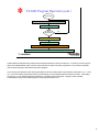
Tutorial Introduction
PURPOSE
- To explain how to configure and program the 68HC08 family FLASH memory.
OBJECTIVES:
- Describe the features and uses of FLASH memory.
- Identify the steps to perform erase and programming operations.
- Describe the methods for programming a blank part.
- Describe standard monitor entry and forced monitor entry.
- Describe the methods for reprogramming a part.
- Describe how to use FLASH as a non-volatile data storage.
CONTENT:
- 32 pages
- 4 questions
LEARNING TIME:
- 40 minutes
PREREQUESITE:
- 68HC08 CPU training module
- Basic understanding of memory types (FLASH, OTP, EEPROM)
m
Semiconductor Products Sector
Welcome to this tutorial on the 68HC08 FLASH memory. This tutorial describes the features of
FLASH memory and how to program it. Please note that on subsequent pages, you will find reference
buttons in the upper right of the content frame that access additional content.
Upon completion of this tutorial, you’ll be able to identify the steps to erase and program the FLASH
and use FLASH as a non-volatile data storage. You’ll also be able to describe the different methods
for entering monitor mode, programming a blank part, and reprogramming a part.
The prerequisite for this tutorial is the 68HC08 CPU training module. It is also assumed that you have
a basic understanding of memory types, such as FLASH, OTP, and EEPROM. Click the Forward
arrow when you’re ready to begin the tutorial.
1
FLASH Memory Features
•
•
•
•
•
In-circuit programming in both user and monitor modes
Small-block programming and erase capability
Internal charge pump sources programming voltage
Built-in FLASH security feature
Block protection against code modification
m
Semiconductor Products Sector
Let’s begin this tutorial with an overview of the features of FLASH memory. Motorola has used several types of FLASH
technology in its microcontrollers. We’ll focus our discussion on the latest incarnation, called split-gate or second
generation FLASH. This type of FLASH is also referred to as TSMC FLASH, where TSMC refers to one of the sites
where the part is manufactured. In general, FLASH memory provides an application with some very important
advantages to support product design, use, and maintenance.
FLASH offers in-circuit programming in both user mode and monitor mode. In-circuit programming is becoming the
preferred means of programming devices in a production environment. This feature makes maintaining and updating
application code an efficient and unobtrusive operation. You can even perform these types of operations through a
remote telephone link, a wireless RF link, or an infrared link.
Small-block programming and erase capability allows for flexible and creative reprogramming schemes. This allows you
to erase and reprogram only what you need to instead of having to reprogram the entire array. Using this method, an
application can continue to operate normally at the same time that the software is being updated.
FLASH includes an internal charge pump that eliminates the need for a separate high voltage supply for programming.
This reduces component cost as well as PC board complexity. FLASH also includes a built-in security mechanism that
provides protection against competitors or hackers from stealing the most important and proprietary part of your product,
your software.
Block protection is another form of protection that helps you to avoid inadvertent code modification. With block
protection, you can select the area of the FLASH array to protect. You can also select to override this protection under
certain hardware configurations. This feature protects against unintentional or malicious attempts to change or destroy
your program. It also protects against runaway code that may execute in FLASH from erasing or reprogramming the
array.
2
Split-gate FLASH Advantages
•
•
•
•
•
Faster programming time (30-40uS per byte)
Better endurance - 10,000 program/erase cycles
Simpler programming algorithm
More flexible block protection
Efficient single-byte programming
m
Semiconductor Products Sector
Next, let’s discuss the advantages offered by split-gate FLASH.
Split-gate FLASH provides faster programming time. It takes 30-40 uS to program each byte. This means
that the actual programming time to program an entire 8 kbyte array is about a quarter of a second.
Additionally, split-gate FLASH offers you better endurance. This type of FLASH can withstand at least 10,000
program/erase cycles across the full range of operating temperatures. This is a big improvement over older
technologies that provide about 100 program/erase cycles at room temperature.
Split-gate FLASH uses a simplified programming algorithm. To program a row of bytes, you simply turn on
the internal high-voltage, apply it to the row, and then write values to each byte in the row. This differs from
past technology which required you to use an iterative process of turning on the high voltage, applying it to a
page, writing values to each byte in the page, checking all bytes for valid values in a “margin” read condition,
and then repeating the process until all of the bytes are programmed.
Split-gate FLASH includes more flexible block protection options, allowing you to specify a finer level of
granularity for protection. Most Split-gate FLASH devices offer 256 different block protection configurations.
Efficient, single-byte programming enables you to use FLASH memory for purposes other than program
memory. Because of the structure of split-gate FLASH and its greater endurance, you can allocate a portion
of the array for non-volatile data storage, thereby eliminating the need for off-chip EEPROM or battery-backed
RAM.
3
68HC908GP32 FLASH Memory Map
0xFFF6 - 0xFFFD
Monitor Mode
entry code addresses
User defined Interrupt
& Reset Vectors
0xFFDC - 0xFFFF
Block Protect Register
0xFF7E
FLASH Control Register
0xFE08
User FLASH memory
0x8000 - 0xFDFF
m
Semiconductor Products Sector
Let’s look next at how FLASH memory is organized. FLASH memory in 68HC08 MCUs is usually an array of
either 8192 or 32,768 eight-bit bytes. The FLASH array is always mapped at the top of the 64k memory map.
This means that an 8k array is mapped from $E000 to $FFFF. The figure shows the 68HC908GP32 32k array
in which FLASH is mapped from $8000 to $FFFF.
Monitor ROM and some reserved locations also reside in this range, so the number of available FLASH
locations will be about 500 bytes less than the full 8k or 32k array size. There is a reserved area for a vector
table at the high address range of the FLASH array. The size and content of the vector table is specific to each
part. To determine the exact locations available for program memory and the vector table in your device,
consult the memory map in the device technical data book.
Split-gate FLASH is usually programmed a row at a time and erased either on a page basis or mass erased. A
page always contains two equally sized rows. The size of the page is typically 64 or 128 bytes, depending on
the size of the FLASH array.
68HC08 MCUs have a built-in charge pump to program and erase the FLASH, so an external power supply is
not needed for this purpose. You can apply the internally generated program/erase voltage to the array by
setting bits in the FLASH Control Register (FLCR), a RAM-based register located in upper memory. To
program and erase the FLASH array, you sequentially set the bits in the FLCR and write values to the target
FLASH locations. Note that this procedure requires you to follow strict timing guidelines. Later in the tutorial,
we’ll review erase and programming operations in more detail.
4
FLASH Control Register (FLCR)
HVEN — High-Voltage Enable Bit
1 = High voltage enabled to array and charge pump on
0 = High voltage disabled to array and charge pump off
m
Semiconductor Products Sector
The FLASH control register, FLCR, is usually located at address $FE08 and consists of four bits that enable you to program
or erase FLASH.
When the high-voltage enable bit, HVEN, is set, the high-voltage is applied to a page of the array during an erase or
programming operation.
Set the mass erase control bit, MASS, to mass erase the entire FLASH array.
As implied by their names, set the ERASE bit to perform an erase operation and the PGM bit to perform a program
operation.
5
FLASH Page Erase Operation
1. Set ERASE bit and clear the MASS bit in the FLCR
2. Read the FLBPR
3. Write any data to any FLASH address within the page to be erased
4. Delay for tnvs (min 10 uS)
5. Enable the high voltage by setting the HVEN bit in the FLCR
6. Delay for tERASE (min 1 mS)
7. Clear the ERASE bit in the FLCR
8. Delay for tnvh (min 5 uS)
9. Turn off high voltage by clearing the HVEN bit in the FLCR
10. Delay for trcv (min 1 uS) then memory can be accessed again in read mode
m
Semiconductor Products Sector
Let’s take a detailed look at the procedure for erasing a page of FLASH.
First, set the ERASE bit in the FLCR and keep the other bits in the register cleared. Since this register is located in
extended memory, you can’t use the bit-set (BSET) and bit-clear (BCLR) instructions to toggle the register bits. Instead,
you must use the load-store instructions.
Next, read the block protection register (FLBPR) and then store data to any address within the page to be erased.
After a time delay of 10 us (tNVS), set the HVEN bit in the FLASH control register.
Next, wait for 1 ms (tERASE) and then clear the ERASE bit in the FLCR.
Wait for another 5 us, (tnvh) and turn off the high voltage by clearing the HVEN bit. By the time you return from this
routine, a time tRCV will have elapsed and you can access the FLASH with the erased page.
You must adhere closely to the timing requirements in this procedure. To verify the time values, consult the electrical
specifications section of the user’s manual. After executing this procedure, all the bytes in this page will contain the
erased state value of $FF.
6
FLASH Mass Erase Operation
1. Set ERASE bit and the MASS bit in the FLCR
2. Read the FLBPR
3. Write any data to any FLASH address within the FLASH address range
4. Delay for tnvs (min 10 uS)
5. Enable the high voltage by setting the HVEN bit in the FLCR
6. Delay for tMERASE (min 4 mS)
7. Clear the ERASE bit in the FLCR
8. Delay for tnvhl (min 100 uS)
9. Turn off high voltage by clearing the HVEN bit in the FLCR
10. Delay for trcv (min 1 uS) then memory can be accessed again in read mode
m
Semiconductor Products Sector
The procedure for erasing the entire FLASH array is similar to the page erase procedure, with a few
differences.
In the mass erase operation, you must set the MASS bit in the first step. In step three, write to any location
within the entire FLASH array.
Also, you must elongate the delay times in steps six and eight. In step six, use a delay time equal to the
mass erase time (tMERASE). In step eight, use a delay time equal to the long high voltage hold time (tnvhl).
7
FLASH Program Operation
1. Set PGM bit in the FLCR
2. Read the FLBPR
3. Write any data to any FLASH address within the row to be programmed
4. Delay for tnvs (min 10 uS)
5. Enable the high voltage by setting the HVEN bit in the FLCR
6. Delay for tPGS (min 5 uS)
Program Steps
m
Semiconductor Products Sector
The FLASH program procedure is a 13-step operation. The figure shows the first six steps. As you can see, the program
procedure is similar to the erase procedures.
The main difference is that the program procedure operates within a row of addresses rather than on a page or the entire
array.
Also, in step 1, you must set the PGM bit rather than the ERASE bit.
8
FLASH Program Operation (cont.)
Program Steps
7. Write data to the FLASH address to be programmed
8. Delay for tPROG (30-40 uS)
9. All
Bytes
Programmed?
No
Yes
10. Clear the PGM bit in the FLCR
11. Delay for tnvh (min 5 uS)
12. Turn off high voltage by clearing the HVEN bit in the FLCR
13. Delay for trcv (min 1 uS) then memory can be accessed again in read mode
m
Semiconductor Products Sector
Another difference between this procedure and the erase procedures is the loop in steps 7-9. In the loop, we write a byte of
data to the desired address, delay, and then verify that all of the bytes have been programmed. This process is repeated
until we finish writing all of the locations we want to program.
You must pay close attention to the timing requirements for all of the delay steps in the procedure (see steps 4, 6, 8, 11, and
13). If you don’t allow enough time during any of these steps, you risk programming the locations incorrectly. If the delays
are too long, you can disturb neighboring locations by programming bits erroneously. Perhaps a more important
consideration is that you risk shortening the life of the array when this occurs.
9
GP32 FLASH Block Protect Register
(FBPR)
Address: $FF7E
Initial value from
factory is $FF.
m
Semiconductor Products Sector
Now that we’ve reviewed the procedures for programming and erasing FLASH, let’s discuss another important concept
called FLASH block protection. Block protection enables you to protect an entire array, or a portion of an array, from
being erased or reprogrammed. This protection is implemented using the FLASH block protect register (FLBPR), itself a
FLASH location.
The value in the FLBPR determines how much of the array will be protected. That is, the bits in the FLBPR specify eight
bits of a 16-bit start address of the block to be protected. The figure shows the block protection scheme for the GP32.
In this scheme, the first bit, bit 15, of the start address is set to 1, bits 14-7 are determined by the content of the FLBPR,
and bits 6-0 are set to 0. With this mechanism, the block protect start address can be $xx00 or $xx80 (128 byte page
boundaries) within the FLASH memory, where 'xx' can be any value from 80 to FF. The only exception to this model is
that a value of $FF in the FLBPR will result in the entire array being unprotected, rather than protecting from $FF80 $FFFF, as might be expected. Also note that the last address of the protected block is always the end of the FLASH
memory, $FFFF.
10
Examples of FLBPR Start Address
m
Semiconductor Products Sector
Let’s look at a few examples using the 908GP32. If the FLBPR contains a value of $00, then the entire array is
protected. If the register contains a value of $01, then the protected area is $8080 - $FFFF. If the register contains a
value of $FE, then the protected area is $FF00-$FFFF. For the GP32, each increment of the FLBPR value decreases
the protected area by 128 bytes. The amount by which the protected area decreases depends on the device. Consult
the technical data book for the specific protection scheme for your device. When the FLBPR contains a value of $FF,
the entire array is unprotected.
The FLBPR is erased and programmed the same way as any other FLASH location. The only way to turn-off or change
the block protection range is to apply the high voltage, around VDD + 2.5v, to the external IRQ pin. When this condition
exists, you can erase the FLBPR. This frees the formerly protected range making it available for erasing and
reprogramming.
11
68HC08 Monitor Features
• Single port pin used for serial communications
• Normal user-mode pin functionality
• Monitor commands
- READ, WRITE, IREAD, IWRITE, READSP, RUN
• Execution of code in RAM or FLASH
• FLASH memory programming interface
- Programming out-of-circuit
- Programming in-circuit
• FLASH memory security
m
Semiconductor Products Sector
Next, let’s discuss entering and using monitor mode beginning with an overview of the monitor features. Monitor mode
is available on all 68HC08 devices. Monitor mode is primarily used to provide serial access to the device and its internal
modules for programming, reading, debugging, and testing activities. You must use this mode to program a blank
device. This is accomplished on a single port pin while still retaining all other user mode pin functionality.
The monitor includes six powerful commands that enable you to implement some important features. These features
include downloading a program into RAM and initiating program execution, and interfacing with the device to perform inor out-of-circuit programming. The monitor also includes a security scheme that reduces the possibility of unauthorized
access to your code.
Let’s discuss each of these features in more detail beginning with the monitor commands.
12
Monitor Mode Commands
Command
Description
Opcode
Data returned
Operand
READ
Read byte from memory
$4A
Returns contents of specified
address
2-byte address in highbyte:low-byte order
WRITE
Write byte to memory
$49
None
2-byte address in highbyte:low-byte order; low-byte
followed by data byte
IREAD
Read next 2 bytes in
memory from last
address accessed
$1A
Returns next 2 bytes in
memory from last address
accessed
2-byte address in highbyte:low-byte order
IWRITE
Write to last address
accessed + 1
$19
None
Single data byte
READSP
Reads stack pointer
$0C
Returns 2-byte address of
stack pointer in high-byte:lowbyte order
None
RUN
Executes PULH and RTI
instructions
$28
Executes PULH and RTI
instructions
None
m
Semiconductor Products Sector
Most monitor mode functions are typically performed by downloading a program into RAM and then executing it.
This is facilitated by six monitor commands.
To read a particular address, enter the READ command followed by the address. The monitor returns the value
stored at the address. To write to a particular address, enter the WRITE command, followed by the address you
want to write to, and then the data that you want to write.
The IREAD command requires no operands and returns the next two bytes from the last address accessed. The
IWRITE command writes a single data-byte to the last address that was accessed incremented by one. The
READSP command requires no operands and returns the two-byte location of the stack pointer.
The RUN command requires no operands and executes the PULH and RTI instructions. Note that executing these
instructions sets the program counter to a new location based on what is stacked. Therefore, you should set the
values of the locations on the stack before using the RUN command. Setting these values effectively will set the
context when the RTI instruction executes.
One final note, you should consult the user’s manual for information about proper timing when communicating with
the monitor.
13
FLASH Programming
• Programming a blank part
- Out-of-circuit monitor mode
- In-circuit monitor mode with standard monitor entry
- In-circuit monitor mode with forced monitor entry
• Reprogramming a part
- User mode
- User mode and monitor mode
- Monitor mode with standard monitor entry
m
Semiconductor Products Sector
Next, let’s look at how to program FLASH. As we discussed earlier, you must use monitor mode to
program a blank part. There are two methods available to you: out-of-circuit programming and incircuit programming. Out-of-circuit programming is by far the easiest method to use. However, if you
want more programming control, you should use in-circuit programming. When using in-circuit
programming, you must satisfy entry mode requirements using either standard monitor entry or forced
monitor entry. Forced monitor entry is a new, convenient alternative to standard monitor entry.
Once the FLASH is programmed, there are three methods you can use to reprogram the part. We’ll
discuss each of these procedures in detail, beginning with the methods for programming a blank part.
14
Out-of-circuit Programming Tools
See: http://www.mcu.motsps.com/documentation/68HC08/devhc08.html
m
Semiconductor Products Sector
The easiest method to program a blank part is out-of-circuit programming. With this method, you don’t
have to follow programming procedures or satisfy monitor mode entry requirements. The programmer
takes care of these details. To program out-of-circuit, simply connect your device to the programmer,
load the s-record file, and then press a button. Your device will be programmed in a matter of
seconds.
Motorola provides in-circuit simulators for many of the newer 68HC08 devices to support out-of-circuit
programming. For other devices, programming support is provided by the SPGMR08 interface
module, the appropriate adapter board, and MCUscribe software. Information about development
tools is provided at the 68HC08 documentation Web site
(http://www.mcu.motsps.com/documentation/68HC08/devhc08.html). In particular, the Microcontroller
Development Tool Selector Guide describes the options that are available to program your device.
This document lists Motorola programming solutions as well as third-party programming support.
Next, let’s look at how to program a blank part using in-circuit programming.
15
Monitor Mode Entry
• Set pins to specific voltages during reset
• Standard monitor entry
- Supported in all 68HC08 devices
- Device can be clocked at user mode frequencies
- Select the clock frequency based on desired baud rate
• Forced monitor entry
- Includes a simplified interface
- Referred to as “FLASHwire programming”
• Security feature
- Valid code entered: memory read, erase, and
programming are available
- Invalid code entered: only mass-erase is available
- Access to other device modules is unaffected
m
Semiconductor Products Sector
In-circuit programming is the preferred method for programming a blank part. Although the monitor is a very
simple device, you must satisfy all entry conditions to access it. These conditions are satisfied by setting the
pins to specific voltages during reset. The two ways to enter monitor mode are standard monitor entry and
forced monitor entry.
All 68HC08 devices support standard monitor entry. Using this method, the device can be clocked at any
frequency within the range allowed in user mode. However, to facilitate communication between the device
and the host, the clock must be selected such that an achievable baud rate will result. In most 68HC08
devices, the baud rate is equal to the internal operating frequency divided by 256. A typical external clock
frequency is 4.9152 MHz, which yields the common baud rate of 9600 bits per second.
Most of the newer 68HC08 devices support a simplified method for entering monitor mode called forced
monitor entry. Because of its simplified interface concept, this method supports what has been coined
“FLASHwire programming”.
A security feature provides protection against unauthorized access to program memory. During monitor
mode entry, the host device is required to enter a security code in the form of eight bytes of data. The
entered value is compared to the value in location $FFF6-$FFFD. If the values match, you can read, erase,
or program the memory. If the values don’t match, access to program memory is prohibited. In this case,
the only operation you can perform on a FLASH-based 68HC08 is a mass erase of the entire FLASH array.
Note that all other device modules, including RAM, are available for inspection and use regardless of FLASH
security access.
Let’s look at some specific examples of programming a blank part.
16
908GP32 Monitor Mode Circuit
m
Semiconductor Products Sector
908GP32 Monitor Mode Circuit, Part 1
Let’s look at standard monitor entry using the 908GP32 monitor mode circuit as a reference. These requirements are
generally the same for all 68HC08 devices. However, you should check the device technical data book to determine the exact
pin configuration for entering monitor mode.
For the GP32, the monitor mode entry pins, port C0 and port C1, are tied high and low respectively.
Port C3 specifies whether the internal frequency is the oscillator frequency divided by 2 or divided by 4. The four switches
shown in this schematic are meant to show different configurations rather than representing actual switches in the circuit.
We‘ll describe the different configuration options that can be selected by referencing these four switches. For the port C3
setting, SW1 is set to position A to divide by 4 and set to position B to divide by 2. To simplify the monitor mode interface, this
option is not offered in many 68HC08 devices. Rather, the internal frequency is always the external frequency divided by 4 as
in user mode.
Another condition for standard monitor entry is high voltage, VTST, on the IRQ pin. On some devices, you may see this voltage
referred to as VDD+VHI. SW2 should be set to position C to apply VTST to IRQ for standard monitor entry. SW2 would be set to
position position D if you are using an external crystal and the internal PLL with a blank part. For information about the voltage
level range for your device, consult the device technical data book.
Note that when SW2 is set to position C, SW3 and SW4 should also be set to their position C. Therefore, for standard monitor
entry, an external oscillator should be connected to OSC1 with VTST applied to the IRQ pin. For forced monitor entry, position
D for SW2, SW3 and SW4 represents the case where OSC1 and OSC2 is connected to a 32.768 kHz crystal circuit with IRQ
grounded to enable the internal PLL on a blank part.
17
908GP32 Monitor Mode Circuit
See figure on page 17
m
Semiconductor Products Sector
908GP32 Monitor Mode Circuit, Part 2
Next, let’s look at the communication pin. For the GP32, this pin is port A0.
Note, you need to use a pull-up resistor on the communication pin. This will keep the dormant state of the communication line
at the appropriate level.
Monitor mode uses bi-directional, non-return to zero, half-duplex communication. This requires multiplexing the host
receive/transmit line, which you can easily implement with a tri-state buffer (MC74HC125).
Another component, the level translator, converts between RS-232 voltage levels and VDD / VSS levels. To reduce component
and manufacturing costs, you can use an intermediate board to perform the multiplexing and level shifting.
On the GP32, when the level of port A7 is tied low, this signals the device that the security code will be entered serially over
port A0.
The alternative method is to use the entire 8-bit port A and enter the code one byte at a time. In some devices, this
functionality is placed on a different pin. In other 68HC08 models, this functionality is consolidated on port A0. For example,
the 908JL3 doesn’t use port A7 to signal serial entry of the security code.
18
Forced Monitor Entry Overview
• Supported in most HC908 devices.
• Monitor mode is entered automatically when the reset vector
is blank.
• JL3 doesn’t require additional configuration.
• GP32 requires these additional configurations:
- Apply voltage to IRQ.
- Set A7 to VSS.
• Not supported in 908AZ60 and 908RK2.
•Consult the device technical data book for information.
m
Semiconductor Products Sector
Most of the newer HC908 devices support forced monitor entry. With this entry method, the part
automatically goes into monitor mode when the part is blank, indicated by a blank reset vector. This
eliminates the need to apply a high voltage to IRQ and the need to satisfy port conditions for monitor
entry. Keep in mind that there may be additional port pin requirements to make the monitor operate
the way you want. For specific information, consult the device technical data book.
For example, on some devices, such as the JL3, no additional port configuration is required for proper
monitor operation. Once in monitor mode, you only need to send the security code over the
communication port (port B0). In other devices, such as the GP32, some of the pins are checked after
monitor mode entry, so you’ll need to configure these appropriately. In the GP32, you can enable or
bypass PLL initialization by setting the IRQ to VSS or VDD respectively. Also, you must set port A7 to
VSS to signify that the security code will be transmitted over the serial communication port (port A0).
In devices that don’t support forced monitor entry, such as the 908AZ60 and the 908RK2, you must
use standard monitor mode entry when programming a blank part. For these devices, you must apply
a high voltage to IRQ and specific polarities to several other port pins. These requirements are the
same for reprogramming a part using standard monitor mode entry. Later in the tutorial, we’ll discuss
reprogramming in more detail.
19
GP32 ISP Interface
VTST or VDD
VDD
GND
IRQ
PTA0
PTA7
RESET
GP and GR families:
OSC
• Clock with 9.8304 MHz oscillator
(IRQ = VDD)
• Clock with 32.768 kHz crystal
(IRQ = VSS)
OSC1
m
Semiconductor Products Sector
GP32 ISP Interface, part 1
The figure shows the forced monitor mode, in-circuit programming interface for the 908GP32. When using forced monitor
entry, the only lines that must come off the target board are the communication line and the ground reference. Depending
on which host programmer you are using, all of the other lines can be controlled on-board as long as they don’t need to
be controlled by the target application. You can control the lines using jumpers, digital switches, or by permanently
hardwiring them to the appropriate polarity. Let’s look at each of these lines in more detail.
When the reset vector is blank, you can enter monitor mode by applying VTST or VDD to IRQ. If VTST is applied, other port
settings may be required to enter monitor mode. If VDD is applied to IRQ, no other port settings are required.
The internal frequency is the external (oscillator) frequency divided by 4, and the communication rate is the internal
frequency divided by 256. The clock source to OSC1 can reside either on the target board, or can be fed in as part of the
programming interface.
In the GP and GR families, you have the option of applying a third voltage to IRQ. In these devices, the part can be
clocked by a low-frequency crystal, typically 32 kHz, and an on-chip PLL. VSS can be applied to IRQ when the reset
vector is blank, in which case the PLL is automatically engaged. The PLL will set the internal frequency to 2.4576 MHz
when the external clock (crystal or oscillator) is 32.768 kHz. In this case, the communication rate is 9600 bits per second.
In this scenario, no other port settings are required.
The ability to clock the device with a low-frequency crystal, and increasing the frequency to a level that produces a
common baud rate, is only available on a blank part. Also, if the PLL is engaged, then the external filtering components
connected to the CGMXFC pin (see the GP32 monitor mode schematics) need to be in place. Application note AN1770,
In-circuit Programming of FLASH Memory in the 68HC908GP20, discusses this and the other monitor mode entry
conditions in detail.
20
GP32 ISP Interface (cont.)
VDD
GND
IRQ
PTA0
PTA7
RESET
GP and GR families:
OSC
• Clock with 9.8304 MHz oscillator
(IRQ = VDD)
• Clock with 32.768 kHz crystal
(IRQ = VSS)
OSC1
m
Semiconductor Products Sector
GP32 ISP Interface, part 2
The communication port, PTA0, can go through the programming interface. Alternatively, it can be tied to the level
translator/multiplexer circuit located either on-board or off-board. Due to concerns for cost and board real estate, you
may chose to exclude these components from the production board. As an alternative, you can include this circuit in an
off-board intermediate assembly which connects the host to the target.
The interface components are not needed when the host doesn’t communicate over an RS-232 link but instead uses the
same voltage levels as PTA0. This is the case when the programming module uses another GP32 to communicate bidirectionally over one of its ports. Whatever the configuration, it’s important to remember that a pull-up resistor must be
connected to the communication port for reliable monitor mode communication.
PTA7 is needed to specify serial entry of the security code. This configuration is not required in some devices such as
the 908JL3.
The reset line is only needed if the host programmer requires it. In most instances, as long as the device is initially put in
monitor mode, the host can program the part without the reset line.
21
In-circuit Programming Tools
• In most cases, you can use out-of-circuit programming tools.
• 68HC08 ICS systems:
- Can be configured to program a device on a target board.
- Supports the mon08 standard mode entry interface.
- Prevents signal contention at the target.
• JL3 and JK3 ICS systems (ICS08JLJK):
- Uses a minimum pin interconnection.
- Hardware and user must prevent signal contention.
• 908AZ60:
- No ICS system available.
- Can use SPGMR08 to connect the target and a PC
running MCUscribe.
• Under special circumstances, write your own host program.
- Host program must adhere to monitor mode requirements.
- See application note AN1770.
m
Semiconductor Products Sector
Now that we’ve learned about in-circuit programming, let’s discuss the tools that can serve as a programming host. In
most situations, the same tools that are used for out-of-circuit programming can be used for in-circuit programming.
Most of the in-circuit simulator (ICS) systems available for the various 68HC08 devices can be configured to program a
device on a target board. All of these ICS systems, at a minimum, support a standard monitor mode entry interface
called mon08. You can implement this interface by providing a header and the necessary connections on the target.
The ICS essentially intercepts the normal user mode connections to the device’s monitor mode pins, and applies the
necessary signals to enter monitor mode and program the device. This type of interconnection prevents the possibility
of signal contention at the target. When the ICS is not connected to the target board’s mon08 header, place jumpers
across the two rows of the header to enable signal flow during normal operation.
Some of the newer ICS systems, such as the ICS08JLJK for the JL3 and JK3, have incorporated a minimum-pin
interconnection for blank part programming. This interface consists of two wires, the communication line and ground,
and depends on the target hardware and the user to assure that there is no signal contention on the communication
line. This ICS also offers a clock output in case it is needed on the target.
Some devices, such as the 908AZ60, don’t have an ICS. One option you have to program this device in-circuit is to
use the SPGMR08 as the intermediate hardware between the target device and a PC running MCUscribe. The
SPGMR08 provides the necessary level translation and muxing for the communication line. Additionally, it provides a
source for the high voltage and a clock suitable for a common baud rate. You can access all of these signals through
one of the adapter board connectors on the SPGMR08 and bring them over to the target board. These connections
essentially reproduce the out-of-circuit programming environment that uses the SPGMR08 and a programming
adapter board.
In some situations, you might find it more suitable to write your own host programming software. For example,
perhaps you want to use a host environment or have unique programming circumstances that are not supported by the
available programming software. In these cases, the host program must adhere closely to monitor mode
communication protocol and bit rate. The standard practice is for the host to download a RAM routine to the device.
This RAM routine would contain the programming routines and a communication executive to receive commands and
data from the host to program the FLASH. Application note AN1770 describes this in detail and offers freeware for
such a host program.
22
Reprogramming with User Mode
VDD
VDD
GND
IRQ
RXD
SCI
TXD
RESET
ClockProgram
with any with
suitable
oscillator
9.8304
32.768MHz
or
kHz
crystal
Oscillator
Crystal
OSC
OSC1
m
Semiconductor Products Sector
Next, let’s review the three methods for reprogramming a device in-circuit, beginning with reprogramming in user mode. We’ll
discuss the advantages of each method and describe the circumstances that make one approach more favorable than the
others.
The most direct method for reprogramming a device is to perform all operations in user mode. This method is preferred over
monitor mode, because you don’t need to implement special hardware configurations. Another advantage is that there is no
inherent communication speed limitation as there is in monitor mode, where the baud rate is a set to a fraction of the internal
frequency.
Let’s look at a specific example of data rates using the 908GP32. When operating at an internal frequency of 7.37 MHz, where
the operating frequency is derived by bumping up a 32.768 kHz crystal frequency with the internal PLL, you can achieve an SCI
baud rate of up to 115.2 kbps. When the selected SCI clock source is a 29.46 MHz external oscillator, you can achieve a baud
rate of 460.8 kbps! The SCI supports many divider values, which gives you a lot of flexibility to select a baud rate, even when
using odd clock frequencies. In addition, the SCI includes built-in error checking capabilities and flexible data size.
Reprogramming a part in user mode is clearly the method of choice for efficient and robust asynchronous communication.
But what if the device that you’re using doesn’t have an SCI? Can you still program in user mode? The answer is ‘yes’. You
can establish an asynchronous communication link the same way you do in monitor mode, by bit-banging over a standard I/O
port pin. Note that there are several application notes that detail the code required for bit-bang communication. This is a very
flexible means of communicating, especially if operating at an odd or very low clock frequency.
An important consideration when reprogramming a device in user mode is block protection. If block protection is turned on, then
VTST on the IRQ is required to turn it off. Block protection would have to be disabled if you wanted to mass erase the entire
device to reprogram it. If you want to erase and reprogram a portion of the array that is not block protected, you could do this
without having to remove block protection from the protected area.
23
Reprogramming with User and
Monitor Modes
1. In user mode:
- clear the reset vector to make the part appear blank, or
- use a mass erase operation.
2. Reset the part, then enter monitor mode using forced monitor
entry.
3. In monitor mode, program the part.
Preferred method under these circumstances:
- Port pin connections are established.
- Device doesn’t include SCI and RAM is small
m
Semiconductor Products Sector
The next method for reprogramming a device in-circuit involves performing operations in both user
mode and monitor mode. For devices that support forced monitor entry, it may be advantageous to
first make the part blank, or appear blank, in user mode. Then, you can use forced monitor entry to
program the part.
As we discussed earlier, forced monitor entry eliminates the need for standard monitor entry
requirements, including VTST on the IRQ. To employ forced monitor entry, the reset vector ($FFFE$FFFF) must be blank. In user mode, first perform a page erase on the vector row or a mass erase
operation, and then reset the device. The device will automatically enter monitor mode using forced
monitor entry. Once in monitor mode, you can perform all programming operations using the
monitor’s communication port.
Although this method uses forced monitor entry, thereby reducing monitor mode entry requirements,
using this scheme still requires you to satisfy some hardware conditions. Given this, there are some
circumstances that make this the preferred method for reprogramming a part in-circuit. For example,
often connections have been already established for port pin communication because the device was
initially programmed in-circuit. Another example would be when the device doesn’t have an SCI and
the size of the RAM is too small to hold both bit-bang communication code and the necessary
programming routines to allow user mode programming.
24
Reprogramming with Standard
Monitor Entry
VTST
VDD
GND
IRQ
PTA0
PTA7
RESET
Clocking with
9.8304 MHz Oscillator
OSC
OSC1
PTC0
PTC3
PTC1
m
Semiconductor Products Sector
The third method for reprogramming a part in-circuit is to perform all program operations in monitor mode
using the standard monitor entry. In standard monitor entry, if the reset vector is not blank, then you must
apply VTST to IRQ. In addition, standard monitor entry requires that you satisfy certain entry mode conditions.
These entry conditions vary from part to part, and may include selecting the division rate for the operating
frequency and pulling a pin low, usually port A7, to select serial entry for the security code. Also, this standard
mode entry doesn’t automatically employ the PLL. This may be of concern in applications where the on-board
clock is a 32.768 kHz crystal. In this case, you need to configure an external clock to drive the device or
communications will start out at a very slow rate, around 32 or 64 baud. This requires the host programmer to
support a slow communication rate. Therefore, it is recommended that you initiate the device PLL as soon as
possible to enable a faster communication rate.
Let’s make a comparison with this method and the second method we discussed that uses a combination of
user and monitor modes to reprogram a part. In the second method, you don’t need to use an external clock
when the on-board clock is 32.768 kHz. This is because with forced monitor mode entry, the IRQ can be
driven to a VSS level. In this case, the PLL is initiated automatically, resulting in a communication rate of 9600
baud.
25
Reprogramming Methods Summary
• Method 1 - User mode
- Preferred method to reprogram a part in-circuit.
- Provides efficient and robust asynchronous communication.
- Can be used with or without an SCI.
•Method 2 - User and monitor modes (forced monitor entry)
- Uses forced monitor mode entry.
- Can be used when device doesn’t include SCI and RAM is small.
•Method 3 - Monitor mode (standard monitor entry)
- Requires you to satisfy all standard entry requirements.
- If the reset vector is not blank, you must apply VTST to IRQ.
- Doesn’t automatically employ the PLL.
m
Semiconductor Products Sector
Take a minute to review the summary of the three methods for reprogramming a part in-circuit. Then
click the Forward arrow to continue the tutorial.
26
ROM-Based FLASH Programming
Routine
Name
Routine
Function
PRGRNGE
Programs a range of locations in FLASH. First
and last addresses and data are passed in RAM
ERARNGE
Erases a page of FLASH, or the entire array.
Erase mode and reference address passed by
parameter.
Reads and verifies a range of locations. Addresses
and compare data passed in RAM
RDVRRNG
Function
GETBYTE
Gets a byte of data from monitor’s communication
port. Does not echo byte received.
DELNUS
Delays for a specified duration. Number of 12 uS
delay quanta and CPU speed passed by parameter.
(See AN1831 for Complete Description)
m
Semiconductor Products Sector
Let’s continue the tutorial with a discussion of ROM-based FLASH programming. For devices
that have a small amount of RAM, FLASH programming routines have been installed in useraccessible ROM. These routines have been installed in a few 68HC08 devices because the
RAM space is too small to hold the programming routine, a communication routine, a data
buffer of any meaningful size, the stack, and application variables. Currently, the 68HC908
devices that include these internal routines are the GR8, KX8, JL3, JK3, JK1, and the JB8.
The ROM-based routines include a routine to program a range, a routine to erase a page or the
entire array, a routine to read and verify a range of FLASH, a routine to receive a byte of data
on the monitor mode communication port, and a delay routine that maintains correct timing
during FLASH erase/program operations.
These routines will help you to minimize development time and write compact RAM routines for
programming and erasing FLASH. The routines support FLASH operation at a wide range of
operating frequencies while maintaining close conformance to the programming specifications.
Even if you are using one of the devices that don’t include these ROM-base routines, they
serve as a good reference for writing your own FLASH programs. For devices that have ample
RAM, such as the 68HC908GP32, you can copy these routines into the your RAM routines.
Application note AN1831 describes how to use these routines and includes calling examples,
routine flow charts, and source code.
27
Using FLASH as a Non-Volatile
Data Storage
•
•
•
•
•
10,000 program/erase cycles
Short program time
Ability to program one byte at a time
Only page or mass erasing is available
Includes software overhead
m
Semiconductor Products Sector
Next, let’s look at how to use FLASH as a non-volatile data storage. Recall that the split-gate architecture
provides at least 10,000 program/erase cycles. Because of this, FLASH memory in HC08 devices offers much
more programming flexibility than past FLASH types. The short programming time and ability to program one
byte at a time enable you to use FLASH as a non-volatile data storage. This application is particularly important
because relatively few controllers in the HC08 family have true EEPROM on-chip . The reason for this is that
EEPROM modules tend to be large in size, requiring a larger die size for the controller, which drives up the cost
of the device.
What limits FLASH from being on the same level as EEPROM is that in FLASH, you can only perform erase
operations on a page or the entire array. FLASH doesn’t include a byte erase operation. Because of this, you
need to be creative when writing software to implement FLASH data storage. Let’s take a look at a specific
example.
28
Example: Data Storage in FLASH
1st
Save
8th
Save
Indicator
Data01
Data02
.
.
.
Data15
Indicator
Data01
Data02
.
.
.
Data15
Indicator
Data01
Data02
.
.
.
Data15
Indicator
Data01
Data02
.
.
.
Data15
Indicator
Data01
Data02
.
.
.
Data15
Indicator
Data01
Data02
.
.
.
Data15
Indicator
Data01
Data02
.
.
.
Data15
Indicator
Data01
Data02
.
.
.
Data15
Data
Block1
Data
Block 2
Data
Block 3
Data
Block 4
Data
Block 5
Data
Block 6
Data
Block 7
Data
Block 8
Data Page -- 128 Bytes
m
Semiconductor Products Sector
Suppose you have 15 bytes of parameters that you want to maintain in non-volatile memory and modify as
needed. Let’s also suppose that you are using the 68HC908GP32 controller. In this controller, a 128-byte
page is the smallest erase block.
First, allocate the entire page to data storage. Rather than erasing the entire page every time you need to
save a modified parameter, write the 15 bytes of parameters to the next 16-byte block in the page. Continue
this process from the first set of parameters at the top of the page to the last set of parameters, storing the last
set at the bottom of the page. This means you can generate up to eight parameter updates before a page
erase is required. This saves time and also helps to maximize the life of the page (remember 10,000
program/erase cycles).
You can track the current data location and the next update location using an indicator byte at the beginning of
the data block. The indicator byte should contain any value other than the erased state value. In split-gate
FLASH, the erased state is $FF, so a logical choice for the indicator value is zero. When the new data is
stored in non-volatile memory, it is also written to the data array in RAM. The copy in RAM is what the
program uses when it needs to access the data.
To find the location of the next update, you can use a routine that searches for the first non-blank ($FF)
indicator byte, starting at the top of the page where the first copy of the data is stored. When you find this
location, write the updated parameters to this block with the indicator set to zero, and then write the updated
parameters to the data array in RAM. If you don’t find a location with a non-blank indicator, this means you
must erase the page and store the new data at the first data block location.
29
Question
Which of the bit strings configures the FLCR for FLASH page erase
operations? Click on your choice.
a) ‘00001111’
b) ‘00001110’
c) ‘00000110’
d) ‘00001010’
m
Semiconductor Products Sector
Let’s complete this tutorial with some questions to check your understanding of the material. Which of the bit strings
configures the FLCR for FLASH page erase operations?
Answer: The bit string in choice d sets the HVEN and ERASE bits to 1, configuring the FLASH for page erase operations.
.
30
Question
In the 908GP32 device, when the FLBPR is set to $02, what range of FLASH
addresses is protected? Click on your choice.
a) The entire FLASH block is protected.
b) $8080 - $FFFF
c) $8100 - $FFFF
d) $FF00 - $FFFF
e) The entire FLASH block is unprotected
m
Semiconductor Products Sector
In the 908GP32 device, when the FLBPR is set to $02, what range of FLASH addresses is protected?
Answer: In the 908GP32 device, setting the FLBPR to $02 selects a start address of $8100. Therefore, the protected
range is $8100 - $FFFF. Note, it is important to remember that the values you use to select the block protect start address
depends on the device. Consult the device technical data book for more information.
31
Question
Which method for reprogramming a part offers the most efficient and robust
asynchronous communication? Click on your choice.
a) Reprogramming in user mode
b) Reprogramming in user and monitor modes
c) Reprogramming in monitor mode with standard entry
m
Semiconductor Products Sector
Which method for reprogramming a part offers the most efficient and robust asynchronous communication?
Answer: In user mode, you can achieve 115.2 kbps using standard clocking methods.
32
Question
Which of the following features make split-gate FLASH a good choice
for non-volatile data storage? Click on your best choice.
a) Better endurance (10,000 program/erase cycles)
b) Ability to program one byte at a time
c) Short programming time
d) All of the above
m
Semiconductor Products Sector
Which of the following features make split-gate FLASH a good choice for non-volatile data storage?
Answer: This is correct, but the best answer is choice d. With 10,000 program/erase cycles, the ability to program one or
many bytes in a page, and a 30 us programming time, split-gate FLASH in the GP32, as well as other HC08 devices, is
well-suited for non-volatile data storage. This eliminates the need and expense of external EEPROM.
33
Tutorial Completion
- FLASH Memory Uses and Features
- Erase and Programming Operations
- Programming a Blank Part.
- Monitor Mode Entry
- Reprogramming a Part
- Using FLASH as a Non-Volatile Data Storage
m
Semiconductor Products Sector
In this tutorial, you’ve learned about the features of the 68HC08 FLASH memory and how to perform erase and
programming operations. You’ve looked at an application for using FLASH as a non-volatile data storage. You’ve also
examined different methods for programming a blank part and reprogramming a part, and the advantages of each method.
34