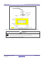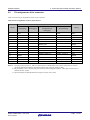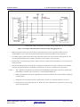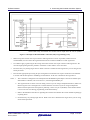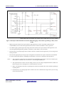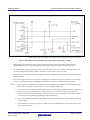
1
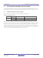
E1/E20 Emulator Additional Document for User’s Manual (Notes on Connection of V850E2M and V850E2S) All information contained in these materials, including products and product specifications, represents information on the product at the time of publication and is subject to change by Renesas Electronics Corp. without notice. Please review the latest information published by Renesas Electronics Corp. through various means, including the Renesas Electronics Corp. website (http://www.renesas.com). Rev.3.00 Oct 2015 Notice 1. Descriptions of circuits, software and other related information in this document are provided only to illustrate the operation of semiconductor products and application examples. You are fully responsible for the incorporation of these circuits, software, and information in the design of your equipment. Renesas Electronics assumes no responsibility for any losses incurred by you or third parties arising from the use of these circuits, software, or information. 2. Renesas Electronics has used reasonable care in preparing the information included in this document, but Renesas Electronics does not warrant that such information is error free. Renesas Electronics assumes no liability whatsoever for any damages incurred by you resulting from errors in or omissions from the information included herein. 3. Renesas Electronics does not assume any liability for infringement of patents, copyrights, or other intellectual property rights of third parties by or arising from the use of Renesas Electronics products or technical information described in this document. No license, express, implied or otherwise, is granted hereby under any patents, copyrights or other intellectual property rights of Renesas Electronics or others. 4. You should not alter, modify, copy, or otherwise misappropriate any Renesas Electronics product, whether in whole or in part. Renesas Electronics assumes no responsibility for any losses incurred by you or third parties arising from such alteration, modification, copy or otherwise misappropriation of Renesas Electronics product. 5. Renesas Electronics products are classified according to the following two quality grades: “Standard” and “High Quality”. The recommended applications for each Renesas Electronics product depends on the product’s quality grade, as indicated below. “Standard”: Computers; office equipment; communications equipment; test and measurement equipment; audio and visual equipment; home electronic appliances; machine tools; personal electronic equipment; and industrial robots etc. “High Quality”: Transportation equipment (automobiles, trains, ships, etc.); traffic control systems; anti-disaster systems; anticrime systems; and safety equipment etc. Renesas Electronics products are neither intended nor authorized for use in products or systems that may pose a direct threat to human life or bodily injury (artificial life support devices or systems, surgical implantations etc.), or may cause serious property damages (nuclear reactor control systems, military equipment etc.). You must check the quality grade of each Renesas Electronics product before using it in a particular application. You may not use any Renesas Electronics product for any application for which it is not intended. Renesas Electronics shall not be in any way liable for any damages or losses incurred by you or third parties arising from the use of any Renesas Electronics product for which the product is not intended by Renesas Electronics. 6. You should use the Renesas Electronics products described in this document within the range specified by Renesas Electronics, especially with respect to the maximum rating, operating supply voltage range, movement power voltage range, heat radiation characteristics, installation and other product characteristics. Renesas Electronics shall have no liability for malfunctions or damages arising out of the use of Renesas Electronics products beyond such specified ranges. 7. Although Renesas Electronics endeavors to improve the quality and reliability of its products, semiconductor products have specific characteristics such as the occurrence of failure at a certain rate and malfunctions under certain use conditions. Further, Renesas Electronics products are not subject to radiation resistance design. Please be sure to implement safety measures to guard them against the possibility of physical injury, and injury or damage caused by fire in the event of the failure of a Renesas Electronics product, such as safety design for hardware and software including but not limited to redundancy, fire control and malfunction prevention, appropriate treatment for aging degradation or any other appropriate measures. Because the evaluation of microcomputer software alone is very difficult, please evaluate the safety of the final products or systems manufactured by you. 8. Please contact a Renesas Electronics sales office for details as to environmental matters such as the environmental compatibility of each Renesas Electronics product. Please use Renesas Electronics products in compliance with all applicable laws and regulations that regulate the inclusion or use of controlled substances, including without limitation, the EU RoHS Directive. Renesas Electronics assumes no liability for damages or losses occurring as a result of your noncompliance with applicable laws and regulations. 9. Renesas Electronics products and technology may not be used for or incorporated into any products or systems whose manufacture, use, or sale is prohibited under any applicable domestic or foreign laws or regulations. You should not use Renesas Electronics products or technology described in this document for any purpose relating to military applications or use by the military, including but not limited to the development of weapons of mass destruction. When exporting the Renesas Electronics products or technology described in this document, you should comply with the applicable export control laws and regulations and follow the procedures required by such laws and regulations. 10. It is the responsibility of the buyer or distributor of Renesas Electronics products, who distributes, disposes of, or otherwise places the product with a third party, to notify such third party in advance of the contents and conditions set forth in this document, Renesas Electronics assumes no responsibility for any losses incurred by you or third parties as a result of unauthorized use of Renesas Electronics products. 11. This document may not be reproduced or duplicated in any form, in whole or in part, without prior written consent of Renesas Electronics. 12. Please contact a Renesas Electronics sales office if you have any questions regarding the information contained in this document or Renesas Electronics products, or if you have any other inquiries. (Note 1) “Renesas Electronics” as used in this document means Renesas Electronics Corporation and also includes its majorityowned subsidiaries. (Note 2) “Renesas Electronics product(s)” means any product developed or manufactured by or for Renesas Electronics. (2012.4) E1/E20 Emulator Contents Contents 1. Outline ............................................................................................................................................................................................4 1.1 Features of an E1 or E20 emulator ........................................................................................................................................................4 1.2 Caution on using the E20 emulator .......................................................................................................................................................4 1.3 Configuration of manuals ........................................................................................................................................................................4 2. Connecting the Emulator and User System ................................................................................................................................. 5 2.1 Connector mounted on the user system ..............................................................................................................................................5 2.2 Pin assignments of the connector .........................................................................................................................................................7 2.3 Examples of recommended connections between the connector and MCU...............................................................................8 2.3.1 Example of recommended connections ........................................................................................................................................8 2.3.2 Connecting the RESET pin .............................................................................................................................................................16 2.3.3 Connecting VDD ................................................................................................................................................................................17 2.3.4 Power supply function (applies only to the E1 emulator) .......................................................................................................18 2.3.5 16-pin conversion adapter for the E1 emulator .........................................................................................................................18 2.3.6 Hot plug-in adapter for the E1 emulator ......................................................................................................................................18 2.3.7 Isolator for the E1 emulator ............................................................................................................................................................18 2.3.8 Small connector conversion adapter for the E1 emulator ......................................................................................................18 2.3.9 14- to 38-pin conversion adapter for the E1 emulator (for the V850) ...................................................................................19 3. Securing Debugging Resources for a Serial OCD Interface ..................................................................................................... 21 3.1 Reset handler ............................................................................................................................................................................................21 3.2 Securing memory areas for debugging ..............................................................................................................................................22 3.3 Securing a serial interface for communications ..............................................................................................................................23 4. Specifications .............................................................................................................................................................................. 24 5. Notes on Usage ........................................................................................................................................................................... 26 5.1 List ...............................................................................................................................................................................................................26 5.2 Details .........................................................................................................................................................................................................27 R20UT1002EJ0300 Oct 01, 2015 Rev.3.00 Page 3 of 34 E1/E20 Emulator 1. Outline 1. Outline 1.1 Features of an E1 or E20 emulator An E1 or E20 emulator (hereafter referred to as an E1/E20) is an on-chip debugging emulator that includes a flash programming function, which is used for debugging and programming programs to be embedded in microcontrollers that have on-chip flash memory. That is, either product can debug a program while the target microcontroller is connected to the user system, and can write programs to the on-chip flash memory of microcontrollers. 1.2 Caution on using the E20 emulator The functions used for debugging of the V850E2M and V850E2S devices by using the E20 emulator are the same as in the E1 emulator. Large trace function, characteristic function of the E20 emulator, cannot be used. The power-supply function from the E20 emulator is not supported. 1.3 Configuration of manuals Documentation for the E1/E20 emulator manual is in two parts: the E1/E20 Emulator User’s Manual and E1/E20 Emulator Additional Document for User’s Manual (this manual). Be sure to read both of the manuals before using the E1/E20 emulator. (1) E1/E20 emulator user’s manual The E1/E20 Emulator User’s Manual describes hardware specifications including the following items: • Components of the emulators • Emulator hardware specifications • Connecting the emulator to a host computer and user system (2) E1/E20 emulator additional document for user’s manual An E1/E20 Emulator Additional Document for User’s Manual describes functions of an emulator debugger, and its contents depend on the given set of MCUs. In general, an additional document has notes on items including the following: • For use in hardware design, an example of connection and the interface circuits required to connect the emulator. • Notes on using the emulator R20UT1002EJ0300 Oct 01, 2015 Rev.3.00 Page 4 of 34 E1/E20 Emulator 2. 2. Connecting the Emulator and User System Connecting the Emulator and User System To connect the E1/E20 emulator, a connector for the user system interface cable must be mounted on the user system. When designing the user system, read this chapter of this manual and the hardware manual for the MCUs to be used. 2.1 Connector mounted on the user system Table 2-1 shows the recommended connectors for connection of the E1/E20 emulator. Table 2-1 Recommended Connectors Type Number 14-pin connector Manufacturer Specification 7614-6002 Sumitomo 3M Limited 14-pin straight type (Japan) 2514-6002 3M Limited 14-pin straight type (other countries) Figures 2-1 shows an example of the connection of the user system interface cable of an E1 emulator to a 14-pin connector. If you intend to use the 14-pin connector, do not mount components with heights exceeding 10 mm within 5 mm of the connector on the user system. If you are using a 16-pin connector, the QB-F14T16-01 adapter (optional product) is available for connection to the user system interface cable. Note that this connector does not support direct connection of an E20 emulator, which has a 38-pin connection. To use an E20 emulator with a 14-pin connector, use the 38-pin/14-pin conversion adapter [R0E000200CKA00] that comes with the E20. R20UT1002EJ0300 Oct 01, 2015 Rev.3.00 Page 5 of 34 E1/E20 Emulator 2. Connecting the Emulator and User System Figure 2-1 Connecting the User System Interface Cable to the 14-pin Connector in the E1/E20 Emulator CAUTION Note on connector insertion and removal: When connecting or disconnecting the user-system interface cable and the emulator or user system, grasp the connector cover at the end of the cable. Pulling the cable itself will damage the wiring. Also, be aware that the user-system interface cable has the direction in which it must be inserted. If the cable is connected in the wrong direction, it may be damaged. R20UT1002EJ0300 Oct 01, 2015 Rev.3.00 Page 6 of 34 E1/E20 Emulator 2.2 2. Connecting the Emulator and User System Pin assignments of the connector Table 2-2 shows the pin assignments of the 14-pin connector. Table 2-2 Pin Assignments of the 14-pin Connector Signal Name (#:active low) Pin No. JTAG LPD UART (= Serial OCD) CSI (Debugging) (Debugging) (Programming & (Programming) I/O (*3) Debugging) 1 TCK - - FPCK Input 2 (*2) GND GND GND GND - 3 TRST# - - - Input 4 - - FLMD0 FLMD0 Input 5 TDO - - FPDT Output 6 - - RESET_IN# - Output 7 TDI LPDIO FPDR FPDR I/O 8 VDD VDD VDD VDD - 9 TMS - (FLMD1) (FLMD1) Input 10 - - RESET_OUT# (*2) RESET_OUT# (*2) Input 11 RDY# - - - Output 12 (*1) GND GND GND GND - 13 RESET_OUT# RESET_OUT# RESET_OUT# (*2) RESET_OUT# (*2) Input 14 (*1) GND GND GND GND - Notes 1. Securely connect pins 2, 12, and 14 of the connector to GND of the user system. These pins are used for electrical GND and to monitor connection with the user system by the E1 or E20. 2. Be particularly sure to connect both pins 10 and 13 before using the emulator. These pins are also used to monitor the user system. 3. Input and output are defined from the perspective of the user system. R20UT1002EJ0300 Oct 01, 2015 Rev.3.00 Page 7 of 34 E1/E20 Emulator 2.3 2. Connecting the Emulator and User System Examples of recommended connections between the connector and MCU This section describes examples of recommended connections between the target device and interface circuit. The supported interfaces differ according to the target device, so check the specifications of the device you are using. 2.3.1 Example of recommended connections Multiple recommended examples for connection are given in accord with the purposes for which the emulator is to be used. Select the appropriate circuit with reference to the table shown below. Be sure to take the specifications of the target device as well as measures to prevent noise into consideration when designing your circuit. Purpose Figure Both debugging (JTAG) and programming (CSI) Figure 2-2 Only debugging (JTAG) Figure 2-3 Only programming (CSI) Figure 2-4 Both debugging (UART) and programming (UART) (serial OCD) Figure 2-5 Only programming (UART) Figure 2-6 Both debugging (LPD) and programming (UART) Figure 2-7 Only debugging (LPD) Figure 2-8 R20UT1002EJ0300 Oct 01, 2015 Rev.3.00 Page 8 of 34 E1/E20 Emulator 2. Connecting the Emulator and User System Caution: Make wiring runs between the connector and the target device as short as possible. Figure 2-2 Example of Recommended Connection (Both Debugging (JTAG) and Programming (CSI)) Make wiring runs between the 14-pin connector and target device as short as possible (within 50 mm is recommended). Do not connect the signal lines between the connector and MCU to other signal lines. Use GND to apply a guard ring for the wiring which runs between the 14-pin connector and target device. Do not route high-speed signal lines parallel to each other or allow them to cross each other. Pin names may vary among target devices. Refer to the user’s manual for the target device you are using for the actual pin names. Proceed with appropriate processing for pins of target devices which do not require connection to the emulator in accord with the descriptions in “Handling of Unused Pins” in the user’s manual for the target device. Notes: 1. This connection is designed on the assumption that the RESET signal output is from an N-channel opendrain buffer. For details, refer to section 2.3.2, Connecting the RESET pin. 2. This signal must be set to the low level during a reset. If you are using a multiplexed function, make sure that this signal is not at the high level on release from the reset state. 3. Refer to the datasheet of the device regarding the resistance and whether the resistor should be pulling up or pulling down. 4. Design the circuit so that this resistor is separated by a switch, etc., when the emulator is not in use. 5. Pin names may vary among target devices. Refer to the user’s manual for the target device you are using for the actual pin names. R20UT1002EJ0300 Oct 01, 2015 Rev.3.00 Page 9 of 34 E1/E20 Emulator 2. Connecting the Emulator and User System Caution: Make wiring runs between the connector and the target device as short as possible. Figure 2-3 Example of Recommended Connection (Only Debugging (JTAG)) Make wiring runs between the 14-pin connector and target device as short as possible (within 50 mm is recommended). Do not connect the signal lines between the connector and MCU to other signal lines. Use GND to apply a guard ring for the wiring which runs between the 14-pin connector and target device. Do not route high-speed signal lines parallel to each other or allow them to cross each other. Pin names may vary among target devices. Refer to the user’s manual for the target device you are using for the actual pin names. Proceed with appropriate processing for pins of target devices which do not require connection to the emulator in accord with the descriptions in “Handling of Unused Pins” in the user’s manual for the target device. Notes: 1. This connection is designed on the assumption that the RESET signal output is from an N-channel opendrain buffer. For details, refer to section 2.3.2, Connecting the RESET pin. 2. Refer to the datasheet of the device regarding the resistance and whether the resistor should be pulling up or pulling down. 3. Design the circuit so that this resistor is separated by a switch, etc., when the emulator is not in use. 4. Pin names may vary among target devices. Refer to the user’s manual for the target device you are using for the actual pin names. R20UT1002EJ0300 Oct 01, 2015 Rev.3.00 Page 10 of 34 E1/E20 Emulator 2. Connecting the Emulator and User System Caution: Make wiring runs between the connector and the target device as short as possible. Figure 2-4 Example of Recommended Connection (Only Programming (CSI)) Make wiring runs between the 14-pin connector and target device as short as possible (within 50 mm is recommended). Do not connect the signal lines between the connector and MCU to other signal lines. Use GND to apply a guard ring for the wiring which runs between the 14-pin connector and target device. Do not route high-speed signal lines parallel to each other or allow them to cross each other. Pin names may vary among target devices. Refer to the user’s manual for the target device you are using for the actual pin names. Proceed with appropriate processing for pins of target devices which do not require connection to the emulator in accord with the descriptions in “Handling of Unused Pins” in the user’s manual for the target device. Notes: 1. This connection is designed on the assumption that the RESET signal output is from an N-channel opendrain buffer. For details, refer to section 2.3.2, Connecting the RESET pin. 2. This signal must be set to the low level during a reset. If you are using a multiplexed function, make sure that this signal is not at the high level on release from the reset state. If you are using a multiplexed function which requires that this signal be pulled up, connect it to pin 9 (FLMD1) of the emulator before it is set to the low level during programming of the flash memory. 3. Refer to the datasheet of the device regarding the resistance and whether the resistor should be pulling up or pulling down. 4. Pin names may vary among target devices. Refer to the user’s manual for the target device you are using for the actual pin names. R20UT1002EJ0300 Oct 01, 2015 Rev.3.00 Page 11 of 34 E1/E20 Emulator 2. Connecting the Emulator and User System Caution: Make wiring runs between the connector and the target device as short as possible. Figure 2-5 Example of Recommended Connection (Both Debugging (UART) and Programming (UART) (Serial OCD)) Make wiring runs between the 14-pin connector and target device as short as possible (within 50 mm is recommended). Do not connect the signal lines between the connector and MCU to other signal lines. Use GND to apply a guard ring for the wiring which runs between the 14-pin connector and target device. Do not route high-speed signal lines parallel to each other or allow them to cross each other. Pin names may vary among target devices. Refer to the user’s manual for the target device you are using for the actual pin names. Proceed with appropriate processing for pins of target devices which do not require connection to the emulator in accord with the descriptions in “Handling of Unused Pins” in the user’s manual for the target device. Notes: 1. This connection is designed on the assumption that the RESET signal output is from an N-channel opendrain buffer. For details, refer to section 2.3.2, Connecting the RESET pin. 2. This signal must be set to the low level during a reset. If you are using a multiplexed function, make sure that this signal is not at the high level on release from the reset state. 3. Refer to the datasheet of the device regarding the resistance and whether the resistor should be pulling up or pulling down. 4. Pin names may vary among target devices. Refer to the user’s manual for the target device you are using for the actual pin names. R20UT1002EJ0300 Oct 01, 2015 Rev.3.00 Page 12 of 34 E1/E20 Emulator 2. Connecting the Emulator and User System Caution: Make wiring runs between the connector and the target device as short as possible. Figure 2-6 Example of Recommended Connection (Only Programming (UART)) Make wiring runs between the 14-pin connector and target device as short as possible (within 50 mm is recommended). Do not connect the signal lines between the connector and MCU to other signal lines. Use GND to apply a guard ring for the wiring which runs between the 14-pin connector and target device. Do not route high-speed signal lines parallel to each other or allow them to cross each other. Pin names may vary among target devices. Refer to the user’s manual for the target device you are using for the actual pin names. Proceed with appropriate processing for pins of target devices which do not require connection to the emulator in accord with the descriptions in “Handling of Unused Pins” in the user’s manual for the target device. Notes: 1. This connection is designed on the assumption that the RESET signal output is from an N-channel opendrain buffer. For details, refer to section 2.3.2, Connecting the RESET pin. 2. This signal must be set to the low level during a reset. If you are using a multiplexed function, make sure that this signal is not at the high level on release from the reset state. If you are using a multiplexed function which requires that this signal be pulled up, connect it to pin 9 (FLMD1) of the emulator before it is set to the low level during programming of the flash memory. 3. Refer to the datasheet of the device regarding the resistance and whether the resistor should be pulling up or pulling down. 4. Pin names may vary among target devices. Refer to the user’s manual for the target device you are using for the actual pin names. R20UT1002EJ0300 Oct 01, 2015 Rev.3.00 Page 13 of 34 E1/E20 Emulator 2. Connecting the Emulator and User System Caution: Make wiring runs between the connector and the target device as short as possible. Figure 2-7 Example of Recommended Connection (Both Debugging (LPD) and Programming (UART)) Make wiring runs between the 14-pin connector and target device as short as possible (within 50 mm is recommended). Do not connect the signal lines between the connector and MCU to other signal lines. Use GND to apply a guard ring for the wiring which runs between the 14-pin connector and target device. Do not route high-speed signal lines parallel to each other or allow them to cross each other. Pin names may vary among target devices. Refer to the user’s manual for the target device you are using for the actual pin names. Proceed with appropriate processing for pins of target devices which do not require connection to the emulator in accord with the descriptions in “Handling of Unused Pins” in the user’s manual for the target device. Notes: 1. This connection is designed on the assumption that the RESET signal output is from an N-channel opendrain buffer (the output resistance is 100 Ω or lower). For details, refer to section 2.3.2, Connecting the RESET pin. 2. This signal must be set to the low level during a reset. If you are using a multiplexed function, make sure that this signal is not at the high level on release from the reset state. If you are using a multiplexed function which requires that this signal be pulled up, connect it to pin 9 (FLMD1) of the emulator before it is set to the low level during programming of the flash memory. 3. Refer to the datasheet of the device regarding the resistance and whether the resistor should be pulling up or pulling down. 4. Pin names may vary among target devices. Refer to the user’s manual for the target device you are using for the actual pin names. R20UT1002EJ0300 Oct 01, 2015 Rev.3.00 Page 14 of 34 E1/E20 Emulator 2. Connecting the Emulator and User System Caution: Make wiring runs between the connector and the target device as short as possible. Figure 2-8 Example of Recommended Connection (Only Debugging (LPD)) Make wiring runs between the 14-pin connector and target device as short as possible (within 50 mm is recommended). Do not connect the signal lines between the connector and MCU to other signal lines. Use GND to apply a guard ring for the wiring which runs between the 14-pin connector and target device. Do not route high-speed signal lines parallel to each other or allow them to cross each other. Pin names may vary among target devices. Refer to the user’s manual for the target device you are using for the actual pin names. Proceed with appropriate processing for pins of target devices which do not require connection to the emulator in accord with the descriptions in “Handling of Unused Pins” in the user’s manual for the target device. Notes: 1. This connection is designed on the assumption that the RESET signal output is from an N-channel opendrain buffer (the output resistance is 100 Ω or lower). For details, refer to section 2.3.2, Connecting the RESET pin. 2. Refer to the datasheet of the device regarding the resistance and whether the resistor should be pulling up or pulling down. 3. Pin names may vary among target devices. Refer to the user’s manual for the target device you are using for the actual pin names. R20UT1002EJ0300 Oct 01, 2015 Rev.3.00 Page 15 of 34 E1/E20 Emulator 2.3.2 2. Connecting the Emulator and User System Connecting the RESET pin Connect the RESET signal as shown in Figure 2-9 if any of the conditions listed below is satisfied. If none of the conditions is satisfied, leave the RESET pin producing the signal output from the emulator open-circuit. • The target device must be kept in the reset state before the debugger is started up and after the debugger is stopped. • The E1/E20 emulator is being used for programming flash memory. • The emulator is using the serial OCD (debugging via a UART). Target device Emulator connector RESET OUT 13 RESET Reset circuit VDD VDD The output from the reset circuit must be N-ch open-drain or a signal generated only by using resistors and capacitors. Figure 2-9 Example of Connecting a Reset Circuit R20UT1002EJ0300 Oct 01, 2015 Rev.3.00 Page 16 of 34 E1/E20 Emulator 2.3.3 2. Connecting the Emulator and User System Connecting VDD Connect VDD of the emulator connector to the power supply pin of the debugging or programming interface on the user system. Use the emulator within the range of power-supply voltages from 1.8 V to 5.5 V and within the operating voltage range of the MCU. The power supply connected to VDD of the emulator connector draws about 10 mA for the power supplies of the first stage input buffer and final stage output buffer of the emulator. If there is a possibility you will be using hot plug-in, you will need to configure the circuit as shown below. Pin 8 (VDD) of the E1/E20 emulator is connected to a 4.7-uF capacitor as shown in Figure 2-10, so hot plug-in connection of the emulator may lead to a momentary drop in the power-supply voltage on the user system. This might cause the MCU to be reset. As shown in Figure 2-11, this effect can be reduced by placing a ferrite bead (or inductor) and relatively large capacitor with low equivalent series resistance near the TVDD line of the connector for connection of the emulator. Note that this measure will not completely eliminate the voltage drop. Hot plug-in is only for use during debugging with a JTAG connection or LPD connection, and requires a hot plug-in adapter that is separately available from Renesas. VDD 4.7 uF Ferrite bead or inductor VDD 8 10 to 47 uF 14-pin connector Figure 2-10 E1/E20 Emulator Internal Circuit R20UT1002EJ0300 Oct 01, 2015 Rev.3.00 Figure 2-11 The Measure Method of E1 Emulator Page 17 of 34 E1/E20 Emulator 2.3.4 2. Connecting the Emulator and User System Power supply function (applies only to the E1 emulator) The E1 emulator can supply power to a system for simple evaluation. It can supply up to 200 mA of current. If you are using the power-supply function of the E1 emulator, check the voltage supplied to the user system. In particular, the 5.0-V supply depends on the USB VBUS power-supply voltage and the voltage might be lower than 5.0 V by 0.5 V or more. Power supply from the E1 emulator depends on the quality of the USB power supply of the host machine, and as such, precision is not guaranteed. When writing a program that requires reliability, do not use the power supply function of the E1 emulator. Use a stable, separate power supply for the user system. When writing a program for mass production processes, use the Flash Development Toolkit or the Renesas Flash Programmer. For details on the flash programming software, refer to http://www.renesas.com/products/tools/flash_prom_programming/ . WARNING Warning for Turning the Power On/Off: When supplying power, ensure that there are no shorts between the user system and power circuit. Only connect the E1 or E20 after confirming that there are no mismatches of alignment on the user system port connector. Incorrect connection will result in the host machine, the emulator, and the user system emitting smoke or catching fire. 2.3.5 16-pin conversion adapter for the E1 emulator When the E1 emulator is connected to a user system having the 16-pin connector, which was supported by the QBMINI2, QB-V850MINI, QB-V850MINIL, PG-FP5, etc., use the 16-pin conversion adapter for the E1 emulator (QBF14T16-01) that is separately available from Renesas. 2.3.6 Hot plug-in adapter for the E1 emulator For hot plug-in connection, use the hot plug-in adapter for the E1 emulator (R0E000010ACB00) that is separately available from Renesas. 2.3.7 Isolator for the E1 emulator For a debugging environment where there is a GND gap between the user system and host PC, use the isolator for the E1 emulator (R0E000010ACB20) that is separately available from Renesas. 2.3.8 Small connector conversion adapter for the E1 emulator The small connector conversion adapter for the E1 emulator (R0E000010CKZ11) is separately available from Renesas for a user system board which is too small to mount the 14-pin connector that is the standard connector for the E1 emulator. By using the adapter, you can reduce the area taken up by the connector mounted on your system. When you use the small connector conversion adapter for the E1 emulator (R0E000010CKZ11), be aware that the connector pin assignments differ from those of the E1 emulator’s standard interface connector. R20UT1002EJ0300 Oct 01, 2015 Rev.3.00 Page 18 of 34 E1/E20 Emulator 2.3.9 2. Connecting the Emulator and User System 14- to 38-pin conversion adapter for the E1 emulator (for the V850) When the E1 emulator is connected to a user system having the Mictor connector, use the 14- to 38-pin conversion adapter for the E1 emulator (QB-F14T38V850-01) that is separately available from Renesas. Table 2-3 shows the pin assignments of the Mictor connector for the V850. Table 2-3 Pin Assignments of the Mictor Connector for the V850 Pin No. 1 2 3 4 5 6 7 8 9 10 11 12 13 14 15 16 17 18 19 20 21 22 23 24 25 26 27 28 29 30 31 32 33 34 35 36 37 38 Signal Name (#: active low) GND GND TCK VDD TMS TRST# TDI RESET_OUT# TDO FLMD0 MSEO0 (*2) RDY# MSEO1 (*2) EVTO# (*2) EVTI# (*2) MCKO (*2) MDO0 (*2) MDO8 (*2) MDO1 (*2) MDO9 (*2) MDO2 (*2) MDO10 (*2) MDO3 (*2) MDO11 (*2) MDO4 (*2) MDO12 (*2) MDO5 (*2) MDO13 (*2) MDO6 (*2) MDO14 (*2) MDO7 (*2) MDO15 (*2) GND GND I/O (*1) Input Input Input Input Input Output Input Output Output Output Output Input Output Output Output Output Output Output Output Output Output Output Output Output Output Output Output Output Output - Notes 1. Input and output are defined from the perspective of the user system. 2. The E1 and E20 emulators do not support event and trace signals from the V850. The E20 emulator has a Mictor connector as a user interface, but this is not connectable to V850 user systems that have been designed according to the pin assignments in Table 2-3. R20UT1002EJ0300 Oct 01, 2015 Rev.3.00 Page 19 of 34 E1/E20 Emulator 2. Connecting the Emulator and User System If you are using an E20 emulator, use the 14- to 38-pin conversion adapter (R0E000200CKA00) that comes with the E20. Connect the user system, QB-F14T38V850-01, R0E000200CKA00, and the E20 emulator in that order. WARNING Warning Regarding Connecting the E20 Emulator to the Mictor Connector: If the E20 emulator is directly connected to the Mictor connector on a V850 user system, the result will be the host machine, the emulator, and the user system emitting smoke or catching fire. R20UT1002EJ0300 Oct 01, 2015 Rev.3.00 Page 20 of 34 E1/E20 Emulator 3. 3. Securing Debug Resources for Serial OCD Interface Securing Debugging Resources for a Serial OCD Interface When a serial OCD interface (debugging through a UART) is in use, the user must prepare the following to handle communications between the E1/E20 emulator and the target device. Refer to the descriptions on the following pages and set these items in the user program or by using compiler options. When using the JTAG or LPD interface, the settings in this section are not required. • Modification of the reset handler • Allocation of memory spaces for debugging • Allocation of a serial interface for communications 3.1 Reset handler The reset handler must include an instruction to jump to the debug monitor program. [Securing the area] It is not necessary to secure this area intentionally. When downloading a program, however, the debugger rewrites the reset vector as described below in the various cases given. If the rewriting pattern does not match the following cases, the software tool is generating an error. • When three nop instructions are consecutively placed from address 0 Before rewriting After rewriting 0x0 nop Instruction to jump to the debug monitor program at 0x0 0x2 nop 0x4 nop 0x6 xxxx 0x6 xxxx • When three 0xFFFFs are consecutively placed from address 0 (applies to erased devices) Before rewriting After rewriting 0x0 0xFFFF Instruction to jump to the debug monitor program at 0x0 0x2 0xFFFF 0x4 0xFFFF 0x6 xxxx 0x6 xxxx • The jr instruction is placed at address 0 (when using the CX compiler from Renesas Electronics) Before rewriting After rewriting 0x0 jr disp22 Instruction to jump to the debug monitor program at 0x0 0x4 xxx 0x6 xxx R20UT1002EJ0300 Oct 01, 2015 0x6 jr disp22 – 6 Rev.3.00 Page 21 of 34 E1/E20 Emulator 3. Securing Debug Resources for Serial OCD Interface • mov32 and jmp are consecutively placed from address 0 Before rewriting After rewriting 0x0 mov imm32,reg1 Instruction to jump to the debug monitor program at 0x0 0x6 jmp [reg1] 0x6 mov imm32,reg1 0xc jmp [reg1] • The instruction to jump to the debug monitor program has been placed at address 0 Before rewriting After rewriting Instruction to jump to the debug monitor program at 0x0 Not changed 3.2 Securing memory areas for debugging Since the shaded areas in Figure 3-1 are the areas reserved for the debugging monitor program, user programs and data cannot be allocated to these areas. These areas must be secured so that they are not used by the user program. Internal ROM area Internal RAM area Internal ROM end address 20 bytes Internal RAM end address 4 Kbytes 6 bytes Vector of received interrupt for debugging (Note 2) 6 bytes 0x60 (interrupt vector for debugging) 6 bytes 0x00 (reset vector) (Note 1) Notes: 1. The debugger automatically allocates this area (refer to section 3.1, Reset handler). 2. This is assigned as a reserved area for the device. Figure 3-1 Memory Areas Required by the Debug Monitor Program R20UT1002EJ0300 Oct 01, 2015 Rev.3.00 Page 22 of 34 E1/E20 Emulator 3.3 3. Securing Debug Resources for Serial OCD Interface Securing a serial interface for communications The debugging monitor program secures a serial interface for communications (by setting the I/O registers). However, a user program changing the settings may lead to an error in communications. To prevent such a problem from occurring, the user program must not change the values set by the debugging monitor program. Settings other than those shown overleaf are prohibited. Do not change bit 0 of any register for port JP0 which is not shown below from its initial value. [Port group JP0] • Port IP control register JPIPC0 • 11 10 9 8 7 6 5 4 3 2 1 0 x x x x x x x x x x x x x x x 0 15 14 13 12 11 10 9 8 7 6 5 4 3 2 1 0 x x x x x x x x x x x x x x x 1 31 30 29 28 27 26 25 24 23 22 21 20 19 18 17 16 x x x x x x x x x x x x x x x x 15 14 13 12 11 10 9 8 7 6 5 4 3 2 1 0 x x x x x x x x x x x x x x x 1 15 14 13 12 11 10 9 8 7 6 5 4 3 2 1 0 x x x x x x x x x x x x x x x 1 15 14 13 12 11 10 9 8 7 6 5 4 3 2 1 0 x x x x x x x x x x x x x x x 1 Port mode control register JPMC0 • 12 Port function control register JPFC0 • 13 Port function control expansion register JPFCE0 • 14 Port open-drain control register JPODC0 • 15 Port bidirectional control register JPBDC0 • x: Any value 15 14 13 12 11 10 9 8 7 6 5 4 3 2 1 0 x x x x x x x x x x x x x x x 1 15 14 13 12 11 10 9 8 7 6 5 4 3 2 1 0 x x x x x x x x x x x x x x x 0 Port mode register JPM0 R20UT1002EJ0300 Oct 01, 2015 Rev.3.00 Page 23 of 34 E1/E20 Emulator 4. 4. Specifications Specifications Specifications are shown in the table below. Broad Category Hardware in general Medium Category Narrow Category Corresponding host machine User system interface Host machine interface Connection to the user system Power supply function (only when the emulator is an E1) Power supply for the emulator Debugging-related items Break*1 Software break Hardware break Event*1 Tracing Performance measurement Forced break Number of events that can be set Available function Combination of events Measurement item Performance Real-time RAM monitoring (RRM) Direct memory modification (DMM) Debugging console Downloading to the external flash memory Hot plug-in Programming-related items R20UT1002EJ0300 Oct 01, 2015 Peripheral breaks Security Clock supply Security flag settings Stand-alone operation Rev.3.00 Specification Computer equipped with a USB port, OS depends on the software 14-pin connector USB 2.0 (full speed or high speed) Connection by the provided user system interface cable 3.3 V or 5.0 V (with current up to 200 mA) can be supplied to the user system (make settings with the debugger) No need (the host computer supplies power through the USB) ROM area: 8 points RAM area: 2000 points 4 points including those used for both execution and access conditions Available 4 points including those used for both execution and access conditions Hardware break only OR, sequential Unavailable From run to break JTAG connection: Resolution: 200 ns, maximum measurement time: 7 minutes Serial OCD connection: Resolution: 100 us, maximum measurement time: 119 hours and 18 minutes LPD connection (Px4-L is in use): (*: CPU clock) Resolution: 100 ns, maximum measurement time: 3.5 minutes (80 MHz*) Resolution: 125 ns, maximum measurement time: 4.5 minutes (64 MHz*) Resolution: 166 ns, maximum measurement time: 6 minutes (48 MHz*) Available*2 Available*2 Unavailable Aavailable (depending on the software) Debugging with JTAG or LPD: Available (requires a hot plug-in adapter separately available from Renesas) Not available with a serial OCD connection Available*3 12-byte ID code authentication Clock on the user system is usable. Available Not available (requires connection to the host machine) Page 24 of 34 E1/E20 Emulator 4. Specifications Notes: 1. The number of breaks that can be set depends on the specification of the device. 2. With a serial connection, short breaks in monitoring or delays in modification will occur. With a JTAG or LPD connection, such short breaks or delays will only occur if the bus is occupied and access is to an area other than the RAM. 3. A function for stopping the operation of peripheral I/O modules during a break is called the peripheral break function. Whether or not peripheral breaks are generated is specifiable in the debugger. For how to specify peripheral breaks, check the manual for the debugger you are using. For selecting whether peripheral breaks can be generated or not, check the manual for the MCU you are using. Details on setting of peripheral breaks (this depends on whether the MCU you are using does or does not support the setting described) • Setting the generation of peripheral breaks by the debugger The SVSTOP bit in the EPC register of the MCU is set to 1. Do not set the EPC register from the user program because the debugger sets this. This setting can be enabled or disabled for individual peripheral modules by the xxxSVSDIS bit in the xxxEMU register. If you require them, make these settings from the user program. For details, check the user’s manual for the MCU you are using. Settings of the EPC and xxxEMU registers will not affect operation while the emulator is not connected. SVSTOP bit in the EPC register xxxSVSDIS bit in the xxxEMU register 0 1 1 * 0 1 R20UT1002EJ0300 Oct 01, 2015 Rev.3.00 Peripheral module during a break Operating Stopped Operating Page 25 of 34 E1/E20 Emulator 5. 5. Notes on Usage Notes on Usage Cautionary notes on using the E1/E20 emulator are given below. 5.1 List Table 5-1 List of Notes on Usage No. 1 Item Handling of devices which were used for debugging 2 Condition for breaks not being usable (serial OCD connection only) 3 Conditions for the pseudo real-time RAM monitor (RRM) and DMM functions not operating (serial OCD connection only) 4 Cancellation of power-save modes (HALT, STOP, and DEEPSTOP modes) 5 Using the DMM function to write values to peripheral I/O registers which require a specific sequence 6 Flash self-programming 7 Operation after a reset (serial OCD connection only) 8 Debugging only with the actual device, i.e. without using an E1/E20 emulator (serial OCD connection only) 9 Multiplexed pin functions for pins of the connection 10 Current drawn 11 Power-saving modes 12 WAKE pin 13 PWGD pin 14 Debugging when the POC function and the power supply are turned off 15 ECC errors 16 Stopping the high-speed internal oscillator (high-speed IntOsc) 17 Iso0 and Iso1 areas 18 Reset through the external pin 19 Hardware breaks in the internal RAM area 20 Quality of flash programming 21 Data read break (Fx4-L series only) 22 Turning the power on/off 23 Note on hot plug-in connection (JTAG or LPD connection only) 24 Note on internal watchdog timer and flash programming 25 Cautionary note on connecting an emulator R20UT1002EJ0300 Oct 01, 2015 Rev.3.00 Page 26 of 34 E1/E20 Emulator 5.2 5. Notes on Usage Details No. 1 Handling of devices which were used for debugging Description: Do not use devices that were used for debugging in mass-production. This is because writing to the flash memory of such devices has already proceeded during debugging, so we cannot guarantee the number of times rewriting of the flash memory can proceed. Software errors occur when programming of the flash memory is no longer possible. Replace the device in such situations. No. 2 Condition for breaks not being usable (serial OCD connection only) Description: Forced breaks are not usable if the following condition is satisfied. • Interrupts are disabled (DI). No. 3 Conditions for the pseudo real-time RAM monitor (RRM) and DMM functions not operating (serial OCD connection only) Description: The pseudo-RRM and DMM functions do not operate if either of the following conditions is satisfied. • Interrupts are currently disabled (DI). • The operating clock differs from that specified in the debugger. No. 4 Release from power-saving modes (HALT, STOP, and DEEPSTOP modes) Description: Using the following functions leads to release from a power-saving mode. • The pseudo-RRM and DMM functions (serial OCD connection only) • Generation of a break No. 5 Using the DMM function to write values to peripheral I/O registers which require a specific sequence Description: The DMM function cannot be used to write to peripheral I/O registers that require a specific sequence of write operations for writing to succeed. No. 6 Flash self-programming Description: With a serial OCD connection If the space containing the debugging monitor program is overwritten by flash self-programming, the debugger will not operate correctly. The following operations must be avoided. - Generation of breaks during flash self-programming - Stepped execution of a program where a step leads to flash self-programming With a JTAG or LPD connection Do not access or have breakpoints set in the ROM area during flash self-programming. No. 7 Operation after a reset (serial OCD connection only) Description: Since the monitor program handles initialization for debugging after a reset, whether due to the signal on the external pin or an internal reset, the time from release from the reset state to execution of the user program differs from that in actual operation of the device. R20UT1002EJ0300 Oct 01, 2015 Rev.3.00 Page 27 of 34 E1/E20 Emulator 5. Notes on Usage No. 8 Debugging only with the actual device, i.e. without using an E1/E20 emulator (serial OCD connection only) Description: For debugging only with an actual device, i.e. without using an E1/E20 emulator, the user program must be programmed by the Renesas flash programmer (RFP). The programs downloaded by the debugger include the monitor program, and this operates incorrectly if it is not controlled by the E1/E20 emulator. No. 9 Multiplexed pin functions for pins of the connection Description: Multiplexed functions for pins of the connection cannot be used during debugging. No. 10 Current drawn Description: The target device consumes more power during debugging than in normal operation since the debugging functions are operating. No. 11 Power-saving modes Description: Before setting isolated areas 0 and 1 (Iso0 and Iso1) to a power-saving mode, clear the wake-up factor masks (WUPMSKH0-WUPMSKH015 and WUPMSKH1-WUPMSKH115) of Iso0 and Iso1, respectively. Before setting only Iso1 to a power-saving mode, clear the wake-up factor masks (WUPMSKH1WUPMSKH115). If these settings are not made, debugger operation is disabled in power-save mode and the debugger may hang. No. 12 WAKE pin Description: The WAKE pin is fixed to the high level in some devices during periods in DeepStop mode and resets. No. 13 PWGD pin Description: The PWGD pin must be fixed to the high level when not in use. Even if the PWGDEN option byte is cleared to 0, handle the PWGD pin by fixing it to the high level when not in use. No. 14 Debugging when the POC function and the power supply are turned off Description: The power supply of the user system must not be turned off during debugging. Check the operation when the POC function and the power supply of the user system are turned off while the emulator is not connected. If the power supply of the user system is even momentarily turned off, the debugger may hang. No. 15 ECC errors Description: In flash self-programming, a program is downloaded to initialize the internal RAM area so that no ECC errors occur. Therefore, ECC errors cannot be emulated after downloading of a program. No. 16 Stopping the high-speed internal oscillator (high-speed IntOsc) Description: Generation of break while the high-speed IntOsc is stopped may cause the debugger to hang. Apply a reset to restore debugger operation. No. 17 Iso0 and Iso1 areas Description: During debugging, power to the Iso0 and Iso1 areas is not shut down during an internal or external reset, or while in deep stop mode (so that values in RAM are retained). R20UT1002EJ0300 Oct 01, 2015 Rev.3.00 Page 28 of 34 E1/E20 Emulator 5. Notes on Usage No. 18 Reset through the external pin Description: Do not allow the generation of a reset in the form of a pin reset other than while the program is in execution. If a reset is generated in this way, the debugger may hang. Even if the reset mask setting in the debugger is for masking, the debugger may still hang. If a pin reset is generated regardless of the above, starting the debugger and connecting the emulator are not possible. No. 19 Hardware breaks in the internal RAM area Description: If a hardware break is set at a location in the internal RAM area, a break will occur when lower-order address bits match and this leads to breaks at unintended positions, as described by the example below. Example: When a break is set at 0x0FED_C000H, breaks will also occur at the following addresses. 0x01ED_C000H, 0x03ED_C000H, 0x05ED_C000H, 0x07ED_C000H, 0x09ED_C000H, 0x0BED_C000H, and 0x0DED_C000H No. 20 Quality of flash programming Description: To improve the quality, follow the guidelines below. • Circuits are designed as described in the user's manuals for the MCU and E1/E20 emulator. • The MCU, E1/E20 emulator, and the software are used as described in respective user's manuals. • The supply of power to the user system is stable. No. 21 Data read break (Fx4-L series only) Description: The data read break is not available on these devices. Do not set data conditions if you are debugging a program on an Fx4-L series device. No. 22 Turning the power on/off Description: Turn the power of the E1/E20 emulator and the user system following the procedure below. When a separate power supply is used for the user system <When using the emulator> (1) Check the power is off. Check that the user system is turned off. When using the E20 emulator, check its power switch is off. (2) Connect the user system. Connect the emulator and the user system with a user-system interface cable. (3) Connect the host machine and turn on the emulator. Connect the emulator and the host machine with a USB interface cable. The E1 emulator is turned on by connecting the USB interface cable. When using the E20 emulator, turn on its power switch. (4) Turn on the user system. Turn on the user system. (5) Launch the emulator debugger. Launch the debugger. R20UT1002EJ0300 Oct 01, 2015 Rev.3.00 Page 29 of 34 E1/E20 Emulator 5. Notes on Usage <When finished using the emulator> (1) Close the emulator debugger. Close the emulator debugger. (2) Turn off the user system. Turn off the user system. (3) Turn off the emulator and disconnect the emulator. When using the E20 emulator, turn off its power switch. Disconnect the USB interface cable from the E1/E20 emulator. The E1 emulator is turned off by disconnecting from the USB interface cable. (4) Disconnecting the user system. Disconnect the user-system interface cable from the user system. CAUTION Notes on the User System Power Supply: While the power of the user system is on, do not turn off the host machine, unplug the USB interface cable, or turn off the power switch of the E20 emulator. The user system may be damaged due to leakage current. When power is supplied to the user system from the emulator (E1 emulator) <When using the emulator> (1) Connect the user system. Connect the emulator and user system with a user-system interface cable. (2) Connect the host machine and turn on the emulator. Connect the emulator and host machine with a USB interface cable, then turn on the emulator. (3) Launch the emulator debugger. Launch the emulator debugger and select the setting of power supply to the user system. <When finished using the emulator> (1) Close the emulator debugger. Close the emulator debugger. (2) Turn off the emulator and disconnect the emulator. Disconnect the USB interface cable from the emulator, then turn off the emulator. (3) Disconnecting the user system. Disconnect the user-system interface cable from the user system. R20UT1002EJ0300 Oct 01, 2015 Rev.3.00 Page 30 of 34 E1/E20 Emulator 5. Notes on Usage No. 23 Note on hot plug-in connection (JTAG or LPD connection only) Description: Hot plug-in connection cannot be used in DeepSTOP mode. No. 24 Note on internal watchdog timer and flash programming Description: When a break is generated while an internal watchdog timer is enabled, and the contents of flash memory are changed by the debugger (downloading or editing from the memory window) and an option byte is read, apply a reset from the debugger before continuing with execution of the program. No. 25 Cautionary note on connecting an emulator Description: When the debugger has been started and an emulator is connected, care must be taken over the period until the emulator generates a break in the MCU, because the program in the MCU will still run (automatically) from the reset vector for a certain time. This still applies in cases where the emulator is connected to the reset pin of the MCU. The program runs for about 3 msec if the connection is JTAG and for about 140 msec if the connection is LPD while the emulator is being released from the reset state until it generates a break in the MCU. This period over which the program runs is called the automatic program-running period, and depends on the environment of the host machine for the E1/E20 emulator. Due to the specifications of the microcontrollers, starting the debugger then connecting an emulator is not possible during a pin or internal reset, or during periods in DeepSTOP mode. To connect the emulator, release the MCU from any pin reset other than from the E1/E20 emulator and ensure that an internal reset is not generated or a transition to DeepSTOP mode is not made during the automatic program-running period described above. When a program that generates an internal reset or causes a transition to DeepSTOP mode running on the MCU is being debugged during the automatic-running period, the contents of the flash memory must be erased once by using the flash programming software (RFP) or a flash programmer (e.g. the PG-FP5). Also, review the setting of the option byte which is used to set operation of the internal watchdog timer as required. R20UT1002EJ0300 Oct 01, 2015 Rev.3.00 Page 31 of 34 E1/E20 Emulator Additional Document for User's Manual (Notes on Connection of V850E2M and V850E2S) Publication Date: Oct 01, 2015 Rev.3.00 Published by: Renesas Electronics Corporation http://www.renesas.com SALES OFFICES Refer to "http://www.renesas.com/" for the latest and detailed information. Renesas Electronics America Inc. 2801 Scott Boulevard Santa Clara, CA 95050-2549, U.S.A. Tel: +1-408-588-6000, Fax: +1-408-588-6130 Renesas Electronics Canada Limited 9251 Yonge Street, Suite 8309 Richmond Hill, Ontario Canada L4C 9T3 Tel: +1-905-237-2004 Renesas Electronics Europe Limited Dukes Meadow, Millboard Road, Bourne End, Buckinghamshire, SL8 5FH, U.K Tel: +44-1628-585-100, Fax: +44-1628-585-900 Renesas Electronics Europe GmbH Arcadiastrasse 10, 40472 Düsseldorf, Germany Tel: +49-211-6503-0, Fax: +49-211-6503-1327 Renesas Electronics (China) Co., Ltd. Room 1709, Quantum Plaza, No.27 ZhiChunLu Haidian District, Beijing 100191, P.R.China Tel: +86-10-8235-1155, Fax: +86-10-8235-7679 Renesas Electronics (Shanghai) Co., Ltd. Unit 301, Tower A, Central Towers, 555 Langao Road, Putuo District, Shanghai, P. R. China 200333 Tel: +86-21-2226-0888, Fax: +86-21-2226-0999 Renesas Electronics Hong Kong Limited Unit 1601-1611, 16/F., Tower 2, Grand Century Place, 193 Prince Edward Road West, Mongkok, Kowloon, Hong Kong Tel: +852-2265-6688, Fax: +852 2886-9022 Renesas Electronics Taiwan Co., Ltd. 13F, No. 363, Fu Shing North Road, Taipei 10543, Taiwan Tel: +886-2-8175-9600, Fax: +886 2-8175-9670 Renesas Electronics Singapore Pte. Ltd. 80 Bendemeer Road, Unit #06-02 Hyflux Innovation Centre, Singapore 339949 Tel: +65-6213-0200, Fax: +65-6213-0300 Renesas Electronics Malaysia Sdn.Bhd. Unit 1207, Block B, Menara Amcorp, Amcorp Trade Centre, No. 18, Jln Persiaran Barat, 46050 Petaling Jaya, Selangor Darul Ehsan, Malaysia Tel: +60-3-7955-9390, Fax: +60-3-7955-9510 Renesas Electronics India Pvt. Ltd. No.777C, 100 Feet Road, HALII Stage, Indiranagar, Bangalore, India Tel: +91-80-67208700, Fax: +91-80-67208777 Renesas Electronics Korea Co., Ltd. 12F., 234 Teheran-ro, Gangnam-Gu, Seoul, 135-080, Korea Tel: +82-2-558-3737, Fax: +82-2-558-5141 © 2015 Renesas Electronics Corporation. All rights reserved. Colophon 4.0 E1/E20 Emulator Additional Document for User’s Manual (Notes on Connection of V850E2M and V850E2S) R20UT1002EJ0300