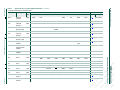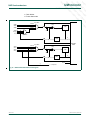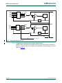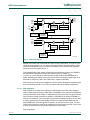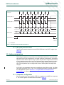
1
D D R R A A A A A FT FT FT FT FT D R R A A FT FT FT FT A A R R D D D D R R A FT FT FT A A R R D D D R A F FT FT A A R R D D User manual D Rev. 01.xx — 5 February 2009 R R R P89LPC9331/9341/9351 User manual D D D UM<nnnnn> D FT FT A A R R D D D R A FT D R A Document information Info Content Keywords P89LPC9331/9341/9351 Abstract Technical information for the P89LPC9331/9341/9351 device D D D D D R R R R R D R R FT R F FT FT A A A D FT FT A A R R D Initial version. D R R 20081118 R A D D 01 D R FT FT A A R R D D D Description FT FT FT FT Date A A A A R R D D D Rev FT FT FT FT FT UM<nnnnn> P89LPC9331/9341/9351 User manual Revision history A A A A A NXP Semiconductors D D R A FT D R A Contact information For more information, please visit: http://www.nxp.com For sales office addresses, please send an email to: [email protected] <Document ID> User manual © NXP B.V. 2009. All rights reserved. Rev. 01.xx — 5 February 2009 2 of 172 D D D D D R R R R R A A A A A D R R FT FT FT FT A A A A R R D D D P89LPC9331/9341/9351 User manual D R R A FT FT FT A A R R D D D R A F FT FT A A R R D D D 1. Introduction FT FT FT FT UM<nnnnn> FT NXP Semiconductors D FT FT A A R R D The P89LPC9331/9341/9351 are single-chip microcontrollers designed for applications demanding high-integration, low cost solutions over a wide range of performance requirements. The P89LPC9331/9341/9351 are based on a high performance processor architecture that executes instructions in two to four clocks, six times the rate of standard 80C51 devices. Many system-level functions have been incorporated into the P89LPC9331/9341/9351 in order to reduce component count, board space, and system cost. D D R A Sector size ADC1 ADC0 PGA0 PGA1 Temp Sensor CCU DATA EEPROM P89LPC9331 4 kB 1 kB X X - - X - - P89LPC9341 4 kB 1 kB X X - - X - - P89LPC9351 8 kB 1 kB X X X X X X X Product Comparison Overview 1.1 Pin configuration P2.0/AD03/DAC0 1 28 P2.7 P2.1/AD02 2 27 P2.6 P0.0/CMP2/KBI0/AD01 3 26 P0.1/CIN2B/KBI1/AD10 P1.7/AD00 4 25 P0.2/CIN2A/KBI2/AD11 P1.6 5 24 P0.3/CIN1B/KBI3/AD12 P1.5/RST 6 23 P0.4/CIN1A/KBI4/DAC1/AD13 VSS 7 P3.1/XTAL1 8 P3.0/XTAL2/CLKOUT 9 P89LPC9331FDH/ P89LPC9341FDH 22 P0.5/CMPREF/KBI5 21 VDD 20 P0.6/CMP1/KBI6 P1.4/INT1 10 19 P0.7/T1/KBI7 P1.3/INT0/SDA 11 18 P1.0/TXD P1.2/T0/SCL 12 17 P1.1/RXD P2.2/MOSI 13 16 P2.5/SPICLK P2.3/MISO 14 15 P2.4/SS 002aae462 Fig 1. P89LPC9331/9341 TSSOP28 pin configuration <Document ID> User manual © NXP B.V. 2009. All rights reserved. Rev. 01.xx — 5 February 2009 3 of 172 A Flash Memory R Device D Product comparison overview FT Table 1. D D D D D R R R R R D R R D R R A FT FT FT A A R R D D D 5 24 P0.3/CIN1B/KBI3/AD12 P1.5/RST 6 23 P0.4/CIN1A/KBI4/DAC1/AD13 VSS 7 P3.1/XTAL1 8 P3.0/XTAL2/CLKOUT 9 D 25 P0.2/CIN2A/KBI2/AD11 P1.6/OCB FT FT A A R R D 4 D D R A FT D R A 22 P0.5/CMPREF/KBI5 21 VDD 20 P0.6/CMP1/KBI6 19 P0.7/T1/KBI7 18 P1.0/TXD 17 P1.1/RXD P2.2/MOSI 13 16 P2.5/SPICLK P2.3/MISO 14 15 P2.4/SS 002aad557 P2.0/ICB/DAC0/AD03 26 P0.1/CIN2B/KBI1/AD10 P2.1/OCD/AD02 1 27 P2.6/OCA P0.0/CMP2/KBI0/AD01 2 28 P2.7/ICA P1.7/OCC/AD00 3 P89LPC9351 TSSOP28 pin configuration 4 Fig 2. P1.6/OCB 5 25 P0.2/CIN2A/KBI2/AD11 P1.5/RST 6 24 P0.3/CIN1B/KBI3/AD12 VSS 7 23 P0.4/CIN1A/KBI4/DAC1/AD13 P3.1/XTAL1 8 P3.0/XTAL2/CLKOUT 9 22 P0.5/CMPREF/KBI5 P89LPC9351FA 21 VDD 20 P0.6/CMP1/KBI6 P1.4/INT1 10 19 P0.7/T1/KBI7 Fig 3. P1.0/TXD 18 002aad558 PLCC28 pin configuration <Document ID> User manual P1.1/RXD 17 P2.5/SPICLK 16 P2.4/SS 15 P2.3/MISO 14 P2.2/MOSI 13 P1.2/T0/SCL 12 P1.3/INT0/SDA 11 © NXP B.V. 2009. All rights reserved. Rev. 01.xx — 5 February 2009 F FT FT 26 P0.1/CIN2B/KBI1/AD10 P1.7/OCC/AD00 A A A 3 R R R 27 P2.6/OCA P0.0/CMP2/KBI0/AD01 D D D 28 P2.7/ICA 2 P1.2/T0/SCL 12 FT FT FT FT 1 P2.1/OCD/AD02 P1.3/INT0/SDA 11 A A A A R R D D D P2.0/ICB/DAC0/AD03 P1.4/INT1 10 FT FT FT FT FT UM<nnnnn> P89LPC9331/9341/9351 User manual P89LPC9351FDH A A A A A NXP Semiconductors 4 of 172 D D D D D R R R R R D R R D R R A FT FT FT A A R R D D D R R A A R Description I/O Port 0: Port 0 is an 8-bit I/O port with a user-configurable output type. During reset Port 0 latches are configured in the input only mode with the internal pull-up disabled. The operation of Port 0 pins as inputs and outputs depends upon the port configuration selected. Each port pin is configured independently. Refer to Section 5.1 “Port configurations” for details. FT FT Type D D R PLCC28, TSSOP28 A FT Port 0 also provides various special functions as described below: P0.0/CMP2/ KBI0/AD01 P0.1/CIN2B/ KBI1/AD10 P0.2/CIN2A/ KBI2/AD11 P0.3/CIN1B/ KBI3/AD12 P0.4/CIN1A/ KBI4/DAC1/AD13 P0.5/CMPREF/ KBI5 P0.6/CMP1/KBI6 P0.7/T1/KBI7 3 26 25 24 23 22 20 19 I/O P0.0 — Port 0 bit 0. O CMP2 — Comparator 2 output I KBI0 — Keyboard input 0. I AD01 — ADC0 channel 1 analog input. I/O P0.1 — Port 0 bit 1. I CIN2B — Comparator 2 positive input B. I KBI1 — Keyboard input 1. I AD10 — ADC1 channel 0 analog input. I/O P0.2 — Port 0 bit 2. I CIN2A — Comparator 2 positive input A. I KBI2 — Keyboard input 2. I AD11 — ADC1 channel 1 analog input. I/O P0.3 — Port 0 bit 3. High current source. I CIN1B — Comparator 1 positive input B. I KBI3 — Keyboard input 3. I AD12 — ADC1 channel 2 analog input. I/O P0.4 — Port 0 bit 4. High current source. I CIN1A — Comparator 1 positive input A. I KBI4 — Keyboard input 4. O DAC1 — Digital-to-analog converter output 1. I AD13 — ADC1 channel 3 analog input. I/O P0.5 — Port 0 bit 5. High current source. I CMPREF — Comparator reference (negative) input. I KBI5 — Keyboard input 5. I/O P0.6 — Port 0 bit 6. High current source. O CMP1 — Comparator 1 output. I KBI6 — Keyboard input 6. I/O P0.7 — Port 0 bit 7. High current source. I/O T1 — Timer/counter 1 external count input or overflow output. I KBI7 — Keyboard input 7. <Document ID> User manual © NXP B.V. 2009. All rights reserved. Rev. 01.xx — 5 February 2009 5 of 172 A All pins have Schmitt trigger inputs. R The Keypad Interrupt feature operates with Port 0 pins. D P0.0 to P0.7 F D D Pin A FT FT A A R R D D D Symbol FT FT FT FT Pin description A A A A R R D D D 1.2 Pin description FT FT FT FT FT UM<nnnnn> P89LPC9331/9341/9351 User manual Table 2. A A A A A NXP Semiconductors D D D D D R R R R R D R R D R A FT FT FT A A R R R R I/O, I Port 1: Port 1 is an 8-bit I/O port with a user-configurable output type, except for three pins as noted below. During reset Port 1 latches are configured in the input only mode with the internal pull-up disabled. The operation of the configurable Port 1 pins as inputs and outputs depends upon the port configuration selected. Each of the configurable port pins are programmed independently. Refer to Section 5.1 “Port configurations” for details. P1.2 to P1.3 are open drain when used as outputs. P1.5 is input only. D FT FT A A R R D D D R A 18 I/O P1.0 — Port 1 bit 0. O TXD — Transmitter output for serial port. P1.1/RXD 17 I/O P1.1 — Port 1 bit 1. I RXD — Receiver input for serial port. I/O P1.2 — Port 1 bit 2 (open-drain when used as output). I/O T0 — Timer/counter 0 external count input or overflow output (open-drain when used as output). I/O SCL — I2C-bus serial clock input/output. I/O P1.3 — Port 1 bit 3 (open-drain when used as output). P1.3/INT0/SDA P1.4/INT1 P1.5/RST P1.6/OCB P1.7/OCC/AD00 12 11 10 6 5 4 P2.0 to P2.7 I INT0 — External interrupt 0 input. I/O SDA — I2C-bus serial data input/output. I/O P1.4 — Port 1 bit 4. High current source. I INT1 — External interrupt 1 input. I P1.5 — Port 1 bit 5 (input only). I RST — External Reset input during power-on or if selected via UCFG1. When functioning as a reset input, a LOW on this pin resets the microcontroller, causing I/O ports and peripherals to take on their default states, and the processor begins execution at address 0. Also used during a power-on sequence to force ISP mode. I/O P1.6 — Port 1 bit 6. High current source. O OCB — Output Compare B.(P89LPC9351) I/O P1.7 — Port 1 bit 7. High current source. O OCC — Output Compare C.(P89LPC9351) I AD00 — ADC0 channel 0 analog input. I/O Port 2: Port 2 is an 8-bit I/O port with a user-configurable output type. During reset Port 2 latches are configured in the input only mode with the internal pull-up disabled. The operation of Port 2 pins as inputs and outputs depends upon the port configuration selected. Each port pin is configured independently. Refer to Section 5.1 “Port configurations” for details. All pins have Schmitt trigger inputs. Port 2 also provides various special functions as described below: P2.0/ICB/DAC0 /AD03 1 I/O P2.0 — Port 2 bit 0. I ICB — Input Capture B.(P89LPC9351) O DAC0 — Digital-to-analog converter output. I AD03 — ADC0 channel 3 analog input. <Document ID> User manual © NXP B.V. 2009. All rights reserved. Rev. 01.xx — 5 February 2009 6 of 172 A P1.0/TXD R Port 1 also provides various special functions as described below: D All pins have Schmitt trigger inputs. FT [1] P1.2/T0/SCL F FT FT Description A A A R R D D D P1.0 to P1.7 D D D Type PLCC28, TSSOP28 FT FT FT FT Pin A A A A R R D D D Pin description …continued Symbol FT FT FT FT FT UM<nnnnn> P89LPC9331/9341/9351 User manual Table 2. A A A A A NXP Semiconductors D D D D D R R R R R D R R D R I AD02 — ADC0 channel 2 analog input. I/O P2.2 — Port 2 bit 2. I/O MOSI — SPI master out slave in. When configured as master, this pin is output; when configured as slave, this pin is input. I/O P2.3 — Port 2 bit 3. I/O MISO — When configured as master, this pin is input, when configured as slave, this pin is output. I/O P2.4 — Port 2 bit 4. I SS — SPI Slave select. I/O P2.5 — Port 2 bit 5. I/O SPICLK — SPI clock. When configured as master, this pin is output; when configured as slave, this pin is input. I/O P2.6 — Port 2 bit 6. O OCA — Output Compare A.(P89LPC9351) I/O P2.7 — Port 2 bit 7. I ICA — Input Capture A.(P89LPC9351) I/O Port 3: Port 3 is a 2-bit I/O port with a user-configurable output type. During reset Port 3 latches are configured in the input only mode with the internal pull-up disabled. The operation of Port 3 pins as inputs and outputs depends upon the port configuration selected. Each port pin is configured independently. Refer to Section 5.1 “Port configurations” for details. R A FT FT D D R A FT D R A Port 3 also provides various special functions as described below: P3.1/XTAL1 9 8 I/O P3.0 — Port 3 bit 0. O XTAL2 — Output from the oscillator amplifier (when a crystal oscillator option is selected via the flash configuration. O CLKOUT — CPU clock divided by 2 when enabled via SFR bit (ENCLK -TRIM.6). It can be used if the CPU clock is the internal RC oscillator, watchdog oscillator or external clock input, except when XTAL1/XTAL2 are used to generate clock source for the RTC/system timer. I/O P3.1 — Port 3 bit 1. I XTAL1 — Input to the oscillator circuit and internal clock generator circuits (when selected via the flash configuration). It can be a port pin if internal RC oscillator or watchdog oscillator is used as the CPU clock source, and if XTAL1/XTAL2 are not used to generate the clock for the RTC/system timer. VSS 7 I Ground: 0 V reference. VDD 21 I Power supply: This is the power supply voltage for normal operation as well as Idle and Power-down modes. [1] Input/output for P1.0 to P1.4, P1.6, P1.7. Input for P1.5. <Document ID> User manual F D A All pins have Schmitt trigger inputs. P3.0/XTAL2/ CLKOUT A OCD — Output Compare D.(P89LPC9351) R P3.0 to P3.1 R P2.1 — Port 2 bit 1. O D 28 D I/O FT Description FT P2.7/ICA 27 A A P2.6/OCA 16 R R P2.5/SPICLK 15 D D P2.4/SS 14 FT FT FT P2.3/MISO 13 A A A P2.2/MOSI 2 R R R P2.1/OCD/AD02 D D D Type PLCC28, TSSOP28 FT FT FT FT Pin A A A A R R D D D Pin description …continued Symbol FT FT FT FT FT UM<nnnnn> P89LPC9331/9341/9351 User manual Table 2. A A A A A NXP Semiconductors © NXP B.V. 2009. All rights reserved. Rev. 01.xx — 5 February 2009 7 of 172 D D D D D R R R R R D R R FT FT FT FT A A A A R R D D D D R R A FT FT FT A A R R D D D R A F FT FT A A R R D D D 1.3 Logic symbols FT FT FT FT FT UM<nnnnn> P89LPC9331/9341/9351 User manual D FT VSS FT A A R R D VDD A A A A A NXP Semiconductors D D R A P89LPC9331/ P89LPC9341 SCL SDA DAC0 AD03 AD02 MOSI MISO SS SPICLK PORT 3 XTAL1 PORT 2 A XTAL2 PORT 1 R CLKOUT PORT 0 TXD RXD T0 INT0 INT1 RST AD00 D CMP2 CIN2B CIN2A CIN1B CIN1A CMPREF CMP1 T1 FT DAC1 KBI0 KBI1 KBI2 KBI3 KBI4 KBI5 KBI6 KBI7 AD01 AD10 AD11 AD12 AD13 002aae461 Fig 4. P89LPC9331/9341 logic symbol VDD DAC1 AD01 AD10 AD11 AD12 AD13 KBI0 KBI1 KBI2 KBI3 KBI4 KBI5 KBI6 KBI7 CMP2 CIN2B CIN2A CIN1B CIN1A CMPREF CMP1 T1 CLKOUT XTAL2 VSS PORT 0 PORT 1 P89LPC9351 PORT 3 XTAL1 PORT 2 TXD RXD T0 INT0 INT1 RST OCB OCC ICB OCD MOSI MISO SS SPICLK OCA ICA SCL SDA AD00 AD03 AD02 DAC0 002aad556 Fig 5. P89LPC9351 logic symbol <Document ID> User manual © NXP B.V. 2009. All rights reserved. Rev. 01.xx — 5 February 2009 8 of 172 D D D D D R R R R R A A A A A D R R FT FT FT FT A A A A R R D D D P89LPC9331/9341/9351 User manual D R R A FT FT FT A A R R D D D R A F FT FT A A R R D D D 1.4 Block diagram FT FT FT FT UM<nnnnn> FT NXP Semiconductors D FT FT A A R R D P89LPC9331/9341/9351 D D R A FT ACCELERATED 2-CLOCK 80C51 CPU D R TXD RXD 256-BYTE DATA RAM I2C-BUS SCL SDA 512-BYTE AUXILIARY RAM(1) SPI internal bus P3[1:0] P2[7:0] PORT 2 CONFIGURABLE I/Os P1[7:0] PORT 1 CONFIGURABLE I/Os P0[7:0] PORT 0 CONFIGURABLE I/Os SPICLK MOSI MISO SS REAL-TIME CLOCK/ SYSTEM TIMER 512-BYTE DATA EEPROM(1) PORT 3 CONFIGURABLE I/Os T0 T1 TIMER 0 TIMER 1 ANALOG COMPARATORS KEYPAD INTERRUPT XTAL1 CRYSTAL OR RESONATOR XTAL2 CONFIGURABLE OSCILLATOR CPU clock ON-CHIP RC OSCILLATOR WITH CLOCK DOUBLER CMP2 CIN2B CIN2A CMP1 CIN1A CIN1B CCU (CAPTURE/ COMPARE UNIT)(1) OCA OCB OCC OCD ICA ICB ADC1/DAC1(2) AD10 AD11 AD12 AD13 DAC1 ADC0/TEMP SENSOR/DAC0(3) AD00 AD01 AD02 AD03 DAC0 WATCHDOG TIMER AND OSCILLATOR PROGRAMMABLE OSCILLATOR DIVIDER A UART 4 kB/8 kB CODE FLASH POWER MONITOR (POWER-ON RESET, BROWNOUT RESET) 002aad555 (1) P89LPC9351 (2) PGA1 on P89LPC9351 (3) PGA0 on P89LPC9351 Fig 6. Block diagram <Document ID> User manual © NXP B.V. 2009. All rights reserved. Rev. 01.xx — 5 February 2009 9 of 172 D D D D D R R R R R A A A A A D R R FT FT FT FT D R R A FT FT FT A A R R D D D R A F FT FT A A R R D D D D FT • User must not attempt to access any SFR locations not defined. • Accesses to any defined SFR locations must be strictly for the functions for the SFRs. • SFR bits labeled ‘-’, ‘0’ or ‘1’ can only be written and read as follows: FT A A R R D Remark: SFR accesses are restricted in the following ways: A A A A R R D D D P89LPC9331/9341/9351 User manual 1.5 Special function registers FT FT FT FT UM<nnnnn> FT NXP Semiconductors D D R A FT D R – ‘0’ must be written with ‘0’, and will return a ‘0’ when read. – ‘1’ must be written with ‘1’, and will return a ‘1’ when read. <Document ID> User manual © NXP B.V. 2009. All rights reserved. Rev. 01.xx — 5 February 2009 10 of 172 A – ‘-’ Unless otherwise specified, must be written with ‘0’, but can return any value when read (even if it was written with ‘0’). It is a reserved bit and may be used in future derivatives. xxxxxxxxxxxxxxxxxxxxx xxxxxxxxxxxxxxxxxxxxxxxxxx xxxxxxx x x x xxxxxxxxxxxxxxxxxxxxxxxxxxxxxx xxxxxxxxxxxxxxxxxxx xx xx xxxxx xxxxxxxxxxxxxxxxxxxxxxxxxxx xxxxxxxxxxxxxxxxxxx xxxxxx xxxxxxxxxxxxxxxxxxxxxxxxxxxxxxxxxxx xxxxxxxxxxxx x x xxxxxxxxxxxxxxxxxxxxx xxxxxxxxxxxxxxxxxxxxxxxxxxxxxx xxxxx xxxxxxxxxxxxxxxxxxxxxxxxxxxxxxxxxxxxxxxxxxxxxxxxxx xxxxxxxx xxxxxxxxxxxxxxxxxxxxxxxxx xxxxxxxxxxxxxxxxxxxx xxx NXP Semiconductors <Document ID> User manual Table 3. Special function registers-P89LPC9331/9341 * indicates SFRs that are bit addressable. Name Description SFR Bit functions and addresses addr. MSB Bit address E7 E6 E5 Reset value LSB E4 E3 E2 E1 Hex Binary 00 0000 0000 E0 Rev. 01.xx — 5 February 2009 A/D control register 0 8EH ENBI0 ENADCI0 TMM0 EDGE0 ADCI0 ENADC0 ADCS01 ADCS00 00 0000 0000 ADCON1 A/D control register 1 97H ENBI1 ENADCI1 TMM1 EDGE1 ADCI1 ENADC1 ADCS11 ADCS10 00 0000 0000 ADINS A/D input select A3H ADI13 ADI12 ADI11 ADI10 ADI03 ADI02 ADI01 ADI00 00 0000 0000 ADMODA A/D mode register A C0H BNDI1 BURST1 SCC1 SCAN1 BNDI0 BURST0 SCC0 SCAN0 00 0000 0000 ADMODB A/D mode register B A1H CLK2 CLK1 CLK0 INBND0 ENDAC1 ENDAC0 BSA1 BSA0 00 000x 0000 AD0BH A/D_0 boundary high register BBH FF 1111 1111 AD0BL A/D_0 boundary low register A6H 00 0000 0000 AD0DAT0 A/D_0 data register 0 C5H 00 0000 0000 AD0DAT1 A/D_0 data register 1 C6H 00 0000 0000 AD0DAT2 A/D_0 data register 2 C7H 00 0000 0000 AD0DAT3 A/D_0 data register 3 F4H 00 0000 0000 AD1BH A/D_1 boundary high register C4H FF 1111 1111 AD1BL A/D_1 boundary low register BCH 00 0000 0000 AD1DAT0 A/D_1 data register 0 D5H 00 0000 0000 D R A FT R FT D D A R FT A R FT D FT R FT D UM<nnnnn> ADCON0 D D D D D R R R R R A A A A A FT FT FT FT FT D D D D R R R R A A A A F F F F T T T T P89LPC9331/9341/9351 User manual D D D D R R R R A A A E0H FT Accumulator A 11 of 172 © NXP B.V. 2009. All rights reserved. ACC* D A R F D A A R FT D xxxxxxxxxxxxxxxxxxxxx xxxxxxxxxxxxxxxxxxxxxxxxxx xxxxxxx x x x xxxxxxxxxxxxxxxxxxxxxxxxxxxxxx xxxxxxxxxxxxxxxxxxx xx xx xxxxx xxxxxxxxxxxxxxxxxxxxxxxxxxx xxxxxxxxxxxxxxxxxxx xxxxxx xxxxxxxxxxxxxxxxxxxxxxxxxxxxxxxxxxx xxxxxxxxxxxx x x xxxxxxxxxxxxxxxxxxxxx xxxxxxxxxxxxxxxxxxxxxxxxxxxxxx xxxxx xxxxxxxxxxxxxxxxxxxxxxxxxxxxxxxxxxxxxxxxxxxxxxxxxx xxxxxxxx xxxxxxxxxxxxxxxxxxxxxxxxx xxxxxxxxxxxxxxxxxxxx xxx Name Description SFR Bit functions and addresses addr. MSB Reset value LSB Hex Binary AD1DAT1 A/D_1 data register 1 D6H 00 0000 0000 AD1DAT2 A/D_1 data register 2 D7H 00 0000 0000 AD1DAT3 A/D_1 data register 3 F5H 00 0000 0000 AUXR1 Auxiliary function register A2H 00 0000 00x0 Bit address NXP Semiconductors <Document ID> User manual Table 3. Special function registers-P89LPC9331/9341 …continued * indicates SFRs that are bit addressable. CLKLP EBRR ENT1 ENT0 SRST 0 - DPS F7 F6 F5 F4 F3 F2 F1 F0 Rev. 01.xx — 5 February 2009 00 0000 0000 Baud rate generator 0 rate low BEH 00 0000 0000 BRGR1[2] Baud rate generator 0 rate high BFH 00 0000 0000 BRGCON Baud rate generator 0 control BDH - - - - - - SBRGS BRGEN 00[2] xxxx xx00 CMP1 Comparator 1 control register ACH - - CE1 CP1 CN1 OE1 CO1 CMF1 00[1] xx00 0000 CMP2 Comparator 2 control register ADH - - CE2 CP2 CN2 OE2 CO2 CMF2 00[1] xx00 0000 DIVM CPU clock divide-by-M control 95H 00 0000 0000 DPTR Data pointer (2 bytes) 00 0000 0000 DPL Data pointer low 82H 00 0000 0000 D 83H FT Data pointer high R DPH A FT R FT D D A R FT A R FT D FT R FT D UM<nnnnn> F0H D A R F D A A R FT D D D D D D R R R R R A A A A A FT FT FT FT FT D D D D R R R R A A A A F F F F T T T T P89LPC9331/9341/9351 User manual D D D D R R R R A A A B register BRGR0[2] A 12 of 172 © NXP B.V. 2009. All rights reserved. B* xxxxxxxxxxxxxxxxxxxxx xxxxxxxxxxxxxxxxxxxxxxxxxx xxxxxxx x x x xxxxxxxxxxxxxxxxxxxxxxxxxxxxxx xxxxxxxxxxxxxxxxxxx xx xx xxxxx xxxxxxxxxxxxxxxxxxxxxxxxxxx xxxxxxxxxxxxxxxxxxx xxxxxx xxxxxxxxxxxxxxxxxxxxxxxxxxxxxxxxxxx xxxxxxxxxxxx x x xxxxxxxxxxxxxxxxxxxxx xxxxxxxxxxxxxxxxxxxxxxxxxxxxxx xxxxx xxxxxxxxxxxxxxxxxxxxxxxxxxxxxxxxxxxxxxxxxxxxxxxxxx xxxxxxxx xxxxxxxxxxxxxxxxxxxxxxxxx xxxxxxxxxxxxxxxxxxxx xxx Name Description SFR Bit functions and addresses addr. MSB Reset value LSB Hex Binary Rev. 01.xx — 5 February 2009 FMADRH Program flash address high E7H 00 0000 0000 FMADRL Program flash address low E6H 00 0000 0000 FMCON Program flash control (Read) E4H BUSY - - - HVA HVE SV OI 70 0111 0000 Program flash control (Write) E4H FMCMD.7 FMCMD.6 FMCMD.5 FMCMD.4 FMCMD.3 FMCMD.2 FMCMD.1 FMCMD.0 FMDATA Program flash data E5H 00 0000 0000 I2ADR I2C-bus slave address register DBH 00 0000 0000 I2CON* I2C-bus 00 x000 00x0 Bit address control D8H NXP Semiconductors <Document ID> User manual Table 3. Special function registers-P89LPC9331/9341 …continued * indicates SFRs that are bit addressable. I2ADR.6 I2ADR.5 I2ADR.4 I2ADR.3 I2ADR.2 I2ADR.1 I2ADR.0 GC DF DE DD DC DB DA D9 D8 - I2EN STA STO SI AA - CRSEL register DDH 00 0000 0000 I2SCLL Serial clock generator/SCL duty cycle register low DCH 00 0000 0000 I2STAT I2C-bus status register D9H F8 1111 1000 IEN0* Interrupt enable 0 00 0000 0000 Bit address A8H STA.4 STA.3 STA.2 STA.1 STA.0 0 0 0 AE AD AC AB AA A9 A8 EA EWDRT EBO ES/ESR ET1 EX1 ET0 EX0 EF EE ED EC EB EA E9 E8 R AF A FT R FT D D A R FT Bit address A R FT D FT R FT D UM<nnnnn> Serial clock generator/SCL duty cycle register high D A R F D A A R FT D D D D D D R R R R R A A A A A FT FT FT FT FT D D D D R R R R A A A A F F F F T T T T P89LPC9331/9341/9351 User manual D D D D R R R R A A A I2SCLH D DAH FT I2C-bus data register A 13 of 172 © NXP B.V. 2009. All rights reserved. I2DAT xxxxxxxxxxxxxxxxxxxxx xxxxxxxxxxxxxxxxxxxxxxxxxx xxxxxxx x x x xxxxxxxxxxxxxxxxxxxxxxxxxxxxxx xxxxxxxxxxxxxxxxxxx xx xx xxxxx xxxxxxxxxxxxxxxxxxxxxxxxxxx xxxxxxxxxxxxxxxxxxx xxxxxx xxxxxxxxxxxxxxxxxxxxxxxxxxxxxxxxxxx xxxxxxxxxxxx x x xxxxxxxxxxxxxxxxxxxxx xxxxxxxxxxxxxxxxxxxxxxxxxxxxxx xxxxx xxxxxxxxxxxxxxxxxxxxxxxxxxxxxxxxxxxxxxxxxxxxxxxxxx xxxxxxxx xxxxxxxxxxxxxxxxxxxxxxxxx xxxxxxxxxxxxxxxxxxxx xxx Name IEN1* Description Interrupt enable 1 SFR Bit functions and addresses addr. MSB E8H Bit address Reset value LSB Hex Binary 00[1] 00x0 0000 EAD EST - - ESPI EC EKBI EI2C BF BE BD BC BB BA B9 B8 IP0* Interrupt priority 0 B8H - PWDRT PBO PS/PSR PT1 PX1 PT0 PX0 00[1] x000 0000 IP0H Interrupt priority 0 high B7H - PWDRTH PBOH PSH/ PSRH PT1H PX1H PT0H PX0H 00[1] x000 0000 FF FE FD FC FB FA F9 F8 Bit address Rev. 01.xx — 5 February 2009 IP1* Interrupt priority 1 F8H PAD PST - - PSPI PC PKBI PI2C 00[1] 00x0 0000 IP1H Interrupt priority 1 high F7H PADH PSTH - - PSPIH PCH PKBIH PI2CH 00[1] 00x0 0000 KBCON Keypad control register 94H - - - - - - PATN _SEL KBIF 00[1] xxxx xx00 KBMASK Keypad interrupt mask register 86H 00 0000 0000 KBPATN Keypad pattern register 93H FF 1111 1111 Bit address Port 0 80H Bit address Port 1 P2* Port 2 90H Bit address A0H 85 84 83 82 81 80 T1/KB7 CMP1 /KB6 CMPREF /KB5 CIN1A /KB4 CIN1B /KB3 CIN2A /KB2 CIN2B /KB1 CMP2 /KB0 97 96 95 94 93 92 91 90 - - RST INT1 INT0/SDA T0/SCL RXD TXD A7 A6 A5 A4 A3 A2 A1 A0 - - SPICLK SS MISO MOSI - - B7 B6 B5 B4 B3 B2 B1 B0 [1] [1] [1] FT [1] Port 3 B0H - - - - - - XTAL1 XTAL2 P0M1 Port 0 output mode 1 84H (P0M1.7) (P0M1.6) (P0M1.5) (P0M1.4) (P0M1.3) (P0M1.2) (P0M1.1) (P0M1.0) FF[1] 1111 1111 P0M2 Port 0 output mode 2 85H (P0M2.7) (P0M2.6) (P0M2.5) (P0M2.4) (P0M2.3) (P0M2.2) (P0M2.1) (P0M2.0) 00[1] 0000 0000 D P3* R A FT R FT D D A R FT A R FT D FT R FT D A 14 of 172 © NXP B.V. 2009. All rights reserved. Bit address 86 UM<nnnnn> P1* 87 D A R F D A A FT D R D D D D D R R R R R A A A A A FT FT FT FT FT D D D D R R R R A A A A F F F F T T T T P89LPC9331/9341/9351 User manual D D D D R R R R A A A P0* NXP Semiconductors <Document ID> User manual Table 3. Special function registers-P89LPC9331/9341 …continued * indicates SFRs that are bit addressable. xxxxxxxxxxxxxxxxxxxxx xxxxxxxxxxxxxxxxxxxxxxxxxx xxxxxxx x x x xxxxxxxxxxxxxxxxxxxxxxxxxxxxxx xxxxxxxxxxxxxxxxxxx xx xx xxxxx xxxxxxxxxxxxxxxxxxxxxxxxxxx xxxxxxxxxxxxxxxxxxx xxxxxx xxxxxxxxxxxxxxxxxxxxxxxxxxxxxxxxxxx xxxxxxxxxxxx x x xxxxxxxxxxxxxxxxxxxxx xxxxxxxxxxxxxxxxxxxxxxxxxxxxxx xxxxx xxxxxxxxxxxxxxxxxxxxxxxxxxxxxxxxxxxxxxxxxxxxxxxxxx xxxxxxxx xxxxxxxxxxxxxxxxxxxxxxxxx xxxxxxxxxxxxxxxxxxxx xxx Name Description SFR Bit functions and addresses addr. MSB NXP Semiconductors <Document ID> User manual Table 3. Special function registers-P89LPC9331/9341 …continued * indicates SFRs that are bit addressable. Reset value LSB Hex Binary 11x1 xx11 Rev. 01.xx — 5 February 2009 Port 1 output mode 1 91H (P1M1.7) (P1M1.6) - (P1M1.4) (P1M1.3) (P1M1.2) (P1M1.1) (P1M1.0) P1M2 Port 1 output mode 2 92H (P1M2.7) (P1M2.6) - (P1M2.4) (P1M2.3) (P1M2.2) (P1M2.1) (P1M2.0) 00[1] 00x0 xx00 P2M1 Port 2 output mode 1 A4H (P2M1.7) (P2M1.6) (P2M1.5) (P2M1.4) (P2M1.3) (P2M1.2) (P2M1.1) (P2M1.0) FF[1] 1111 1111 P2M2 Port 2 output mode 2 A5H (P2M2.7) (P2M2.6) (P2M2.5) (P2M2.4) (P2M2.3) (P2M2.2) (P2M2.1) (P2M2.0) 00[1] 0000 0000 P3M1 Port 3 output mode 1 B1H - - - - - - (P3M1.1) (P3M1.0) 03[1] xxxx xx11 P3M2 Port 3 output mode 2 B2H - - - - - - (P3M2.1) (P3M2.0) 00[1] xxxx xx00 PCON Power control register 87H SMOD1 SMOD0 - BOI GF1 GF0 PMOD1 PMOD0 00 0000 0000 PCONA Power control register A B5H RTCPD - VCPD ADPD I2PD SPPD SPD - 00[1] 0000 0000 D7 D6 D5 D4 D3 D2 D1 D0 PSW* Program status word D0H CY AC F0 RS1 RS0 OV F1 P 00 0000 0000 PT0AD Port 0 digital input disable F6H - - PT0AD.5 PT0AD.4 PT0AD.3 PT0AD.2 PT0AD.1 - 00 xx00 000x RSTSRC Reset source register DFH - BOIF BOF POF R_BK R_WD R_SF R_EX [3] RTCCON RTC control D1H RTCF RTCS1 RTCS0 - - - ERTC RTCEN Bit address 011x xx00 0000 0000 RTC register low D3H 00[6] 0000 0000 SADDR Serial port address register A9H 00 0000 0000 SADEN Serial port address enable B9H 00 0000 0000 D RTCL FT D2H R RTC register high A FT R FT D D A R FT A R FT D FT R FT D A 15 of 172 © NXP B.V. 2009. All rights reserved. RTCH 00[6] UM<nnnnn> 60[1][6] D A R F D A A R FT D D D D D D R R R R R A A A A A FT FT FT FT FT D D D D R R R R A A A A F F F F T T T T P89LPC9331/9341/9351 User manual D D D D R R R R A A A P1M1 D3[1] xxxxxxxxxxxxxxxxxxxxx xxxxxxxxxxxxxxxxxxxxxxxxxx xxxxxxx x x x xxxxxxxxxxxxxxxxxxxxxxxxxxxxxx xxxxxxxxxxxxxxxxxxx xx xx xxxxx xxxxxxxxxxxxxxxxxxxxxxxxxxx xxxxxxxxxxxxxxxxxxx xxxxxx xxxxxxxxxxxxxxxxxxxxxxxxxxxxxxxxxxx xxxxxxxxxxxx x x xxxxxxxxxxxxxxxxxxxxx xxxxxxxxxxxxxxxxxxxxxxxxxxxxxx xxxxx xxxxxxxxxxxxxxxxxxxxxxxxxxxxxxxxxxxxxxxxxxxxxxxxxx xxxxxxxx xxxxxxxxxxxxxxxxxxxxxxxxx xxxxxxxxxxxxxxxxxxxx xxx Name SBUF Description Serial Port data buffer register SFR Bit functions and addresses addr. MSB Reset value LSB 99H Bit address 9F 9E 9D 9C 9B 9A 99 98 Hex Binary xx xxxx xxxx SCON* Serial port control 98H SM0/FE SM1 SM2 REN TB8 RB8 TI RI 00 0000 0000 SSTAT Serial port extended status register BAH DBMOD INTLO CIDIS DBISEL FE BR OE STINT 00 0000 0000 Rev. 01.xx — 5 February 2009 SP Stack pointer 81H 07 0000 0111 SPCTL SPI control register E2H SSIG SPEN DORD MSTR CPOL CPHA SPR1 SPR0 04 0000 0100 SPSTAT SPI status register E1H SPIF WCOL - - - - - - 00 00xx xxxx SPDAT SPI data register E3H 00 0000 0000 TAMOD Timer 0 and 1 auxiliary mode 8FH 00 xxx0 xxx0 00 0000 0000 Bit address NXP Semiconductors <Document ID> User manual Table 3. Special function registers-P89LPC9331/9341 …continued * indicates SFRs that are bit addressable. - - - T1M2 - - - T0M2 8F 8E 8D 8C 8B 8A 89 88 TF1 TR1 TF0 TR0 IE1 IT1 IE0 IT0 Timer 0 high 8CH 00 0000 0000 TH1 Timer 1 high 8DH 00 0000 0000 TL0 Timer 0 low 8AH 00 0000 0000 TL1 Timer 1 low 8BH 00 0000 0000 TMOD Timer 0 and 1 mode 89H T1GATE T1C/T T1M1 T1M0 T0GATE T0C/T T0M1 T0M0 00 0000 0000 TRIM Internal oscillator trim register 96H RCCLK ENCLK TRIM.5 TRIM.4 TRIM.3 TRIM.2 TRIM.1 TRIM.0 [5][6] WDCON Watchdog control register A7H PRE2 PRE1 PRE0 - - WDRUN WDTOF WDCLK [4][6] D R A FT R FT D D A R FT A R FT D FT R FT D UM<nnnnn> TH0 D D D D D R R R R R A A A A A FT FT FT FT FT D D D D R R R R A A A A F F F F T T T T P89LPC9331/9341/9351 User manual D D D D R R R R A A A 88H FT Timer 0 and 1 control A 16 of 172 © NXP B.V. 2009. All rights reserved. TCON* D A R F D A A R FT D xxxxxxxxxxxxxxxxxxxxx xxxxxxxxxxxxxxxxxxxxxxxxxx xxxxxxx x x x xxxxxxxxxxxxxxxxxxxxxxxxxxxxxx xxxxxxxxxxxxxxxxxxx xx xx xxxxx xxxxxxxxxxxxxxxxxxxxxxxxxxx xxxxxxxxxxxxxxxxxxx xxxxxx xxxxxxxxxxxxxxxxxxxxxxxxxxxxxxxxxxx xxxxxxxxxxxx x x xxxxxxxxxxxxxxxxxxxxx xxxxxxxxxxxxxxxxxxxxxxxxxxxxxx xxxxx xxxxxxxxxxxxxxxxxxxxxxxxxxxxxxxxxxxxxxxxxxxxxxxxxx xxxxxxxx xxxxxxxxxxxxxxxxxxxxxxxxx xxxxxxxxxxxxxxxxxxxx xxx Name Description SFR Bit functions and addresses addr. MSB WDL Watchdog load C1H WFEED1 Watchdog feed 1 C2H WFEED2 Watchdog feed 2 C3H NXP Semiconductors <Document ID> User manual Table 3. Special function registers-P89LPC9331/9341 …continued * indicates SFRs that are bit addressable. Reset value LSB Hex Binary FF 1111 1111 Rev. 01.xx — 5 February 2009 [1] All ports are in input only (high-impedance) state after power-up. [2] BRGR1 and BRGR0 must only be written if BRGEN in BRGCON SFR is logic 0. If any are written while BRGEN = 1, the result is unpredictable. [3] The RSTSRC register reflects the cause of the P89LPC9331/9341 reset except BOIF bit. Upon a power-up reset, all reset source flags are cleared except POF and BOF; the power-on reset value is x011 0000. [4] After reset, the value is 1110 01x1, i.e., PRE2 to PRE0 are all logic 1, WDRUN = 1 and WDCLK = 1. WDTOF bit is logic 1 after watchdog reset and is logic 0 after power-on reset. Other resets will not affect WDTOF. [5] On power-on reset and watchdog reset, the TRIM SFR is initialized with a factory preprogrammed value. Other resets will not cause initialization of the TRIM register. [6] The only reset sources that affect these SFRs are power-on reset and watchdog reset. D A FT FT R D A R A R FT D FT R FT D UM<nnnnn> D D D D D R R R R R A A A A A FT FT FT FT FT D D D D R R R R A A A A F F F F T T T T P89LPC9331/9341/9351 User manual D D D D R R R R A A A FT R D FT A 17 of 172 © NXP B.V. 2009. All rights reserved. D A R F D A A R FT D xxxxxxxxxxxxxxxxxxxxx xxxxxxxxxxxxxxxxxxxxxxxxxx xxxxxxx x x x xxxxxxxxxxxxxxxxxxxxxxxxxxxxxx xxxxxxxxxxxxxxxxxxx xx xx xxxxx xxxxxxxxxxxxxxxxxxxxxxxxxxx xxxxxxxxxxxxxxxxxxx xxxxxx xxxxxxxxxxxxxxxxxxxxxxxxxxxxxxxxxxx xxxxxxxxxxxx x x xxxxxxxxxxxxxxxxxxxxx xxxxxxxxxxxxxxxxxxxxxxxxxxxxxx xxxxx xxxxxxxxxxxxxxxxxxxxxxxxxxxxxxxxxxxxxxxxxxxxxxxxxx xxxxxxxx xxxxxxxxxxxxxxxxxxxxxxxxx xxxxxxxxxxxxxxxxxxxx xxx NXP Semiconductors <Document ID> User manual Table 4. Extended special function registers-P89LPC9331/9341 Rev. 01.xx — 5 February 2009 Name Description SFR addr. Bit functions and addresses Reset value BODCFG BOD configuration register FFC8H - - - - - - CLKCON CLOCK Control register FFDEH CLKOK - - XTALWD CLKDBL FOSC2 FOSC1 FOSC0 [3] TPSCON Temperature sensor control register FFCAH - - - - TSEL1 TSEL0 - - 00 0000 0000 RTCDATH Real-time clock data register high FFBFH 00 0000 0000 RTCDATL Real-time clock FFBEH data register low 00 0000 0000 MSB LSB Hex BOICFG1 BOICFG0 Binary [2] [1] Extended SFRs are physically located on-chip but logically located in external data memory address space (XDATA). The MOVX A,@DPTR and MOVX @DPTR,A instructions are used to access these extended SFRs. [2] The BOICFG1/0 will be copied from UCFG1.5 and UCFG1.3 when power-on reset. [3] CLKCON register reset value comes from UCFG1 and UCFG2. The reset value of CLKCON.2 to CLKCON.0 come from UCFG1.2 to UCFG1.0 and reset value of CLKDBL bit comes from UCFG2.7. D A FT FT R D A R A R FT D FT R FT D UM<nnnnn> D D D D D R R R R R A A A A A FT FT FT FT FT D D D D R R R R A A A A F F F F T T T T P89LPC9331/9341/9351 User manual D D D D R R R R A A A FT R D FT A 18 of 172 © NXP B.V. 2009. All rights reserved. D A R F D A A R FT D xxxxxxxxxxxxxxxxxxxxx xxxxxxxxxxxxxxxxxxxxxxxxxx xxxxxxx x x x xxxxxxxxxxxxxxxxxxxxxxxxxxxxxx xxxxxxxxxxxxxxxxxxx xx xx xxxxx xxxxxxxxxxxxxxxxxxxxxxxxxxx xxxxxxxxxxxxxxxxxxx xxxxxx xxxxxxxxxxxxxxxxxxxxxxxxxxxxxxxxxxx xxxxxxxxxxxx x x xxxxxxxxxxxxxxxxxxxxx xxxxxxxxxxxxxxxxxxxxxxxxxxxxxx xxxxx xxxxxxxxxxxxxxxxxxxxxxxxxxxxxxxxxxxxxxxxxxxxxxxxxx xxxxxxxx xxxxxxxxxxxxxxxxxxxxxxxxx xxxxxxxxxxxxxxxxxxxx xxx NXP Semiconductors <Document ID> User manual Table 5. Special function registers-P89LPC9351 * indicates SFRs that are bit addressable. Name Description SFR addr. Bit address Bit functions and addresses Reset value MSB E7 LSB E6 E5 E4 E3 E2 E1 Hex Binary 00 0000 0000 E0 ACC* Accumulator E0H ADCON0 A/D control register 0 8EH ENBI0 ENADCI0 TMM0 EDGE0 ADCI0 ENADC0 ADCS01 ADCS00 00 0000 0000 ADCON1 A/D control register 1 97H ENBI1 ENADCI1 TMM1 EDGE1 ADCI1 ENADC1 ADCS11 ADCS10 00 0000 0000 Rev. 01.xx — 5 February 2009 ADI11 ADI10 ADI03 ADI02 ADI01 ADI00 00 0000 0000 BURST1 SCC1 SCAN1 BNDI0 BURST0 SCC0 SCAN0 00 0000 0000 ADMODB A/D mode register B A1H CLK2 CLK1 CLK0 INBND0 ENDAC1 ENDAC0 BSA1 BSA0 00 000x 0000 AD0BH A/D_0 boundary high register BBH FF 1111 1111 AD0BL A/D_0 boundary low register A6H 00 0000 0000 AD0DAT0 A/D_0 data register 0 C5H 00 0000 0000 AD0DAT1 A/D_0 data register 1 C6H 00 0000 0000 AD0DAT2 A/D_0 data register 2 C7H 00 0000 0000 AD0DAT3 A/D_0 data register 3 F4H 00 0000 0000 AD1BH A/D_1 boundary high register C4H FF 1111 1111 AD1BL A/D_1 boundary low register BCH 00 0000 0000 AD1DAT0 A/D_1 data register 0 D5H 00 0000 0000 AD1DAT1 A/D_1 data register 1 D6H 00 0000 0000 AD1DAT2 A/D_1 data register 2 D7H 00 0000 0000 R A FT R FT D D A R FT A R FT D FT R FT D UM<nnnnn> ADI12 BNDI1 D A R F D A A R FT D D D D D D R R R R R A A A A A FT FT FT FT FT D D D D R R R R A A A A F F F F T T T T P89LPC9331/9341/9351 User manual D D D D R R R R A A A ADI13 C0H D A3H A/D mode register A FT A/D input select ADMODA A 19 of 172 © NXP B.V. 2009. All rights reserved. ADINS xxxxxxxxxxxxxxxxxxxxx xxxxxxxxxxxxxxxxxxxxxxxxxx xxxxxxx x x x xxxxxxxxxxxxxxxxxxxxxxxxxxxxxx xxxxxxxxxxxxxxxxxxx xx xx xxxxx xxxxxxxxxxxxxxxxxxxxxxxxxxx xxxxxxxxxxxxxxxxxxx xxxxxx xxxxxxxxxxxxxxxxxxxxxxxxxxxxxxxxxxx xxxxxxxxxxxx x x xxxxxxxxxxxxxxxxxxxxx xxxxxxxxxxxxxxxxxxxxxxxxxxxxxx xxxxx xxxxxxxxxxxxxxxxxxxxxxxxxxxxxxxxxxxxxxxxxxxxxxxxxx xxxxxxxx xxxxxxxxxxxxxxxxxxxxxxxxx xxxxxxxxxxxxxxxxxxxx xxx Name Description SFR addr. Bit functions and addresses Reset value MSB LSB Hex Binary 00 0000 0000 00 0000 00x0 F5H AUXR1 Auxiliary function register A2H B* B register F0H 00 0000 0000 BRGR0[2] Baud rate generator 0 rate low BEH 00 0000 0000 BRGR1[2] Baud rate generator 0 rate high BFH 00 0000 0000 BRGCON Baud rate generator 0 control BDH - - - - - - SBRGS BRGEN 00[2] xxxx xx00 CCCRA Capture compare A control register EAH ICECA2 ICECA1 ICECA0 ICESA ICNFA FCOA OCMA1 OCMA0 00 0000 0000 CCCRB Capture compare B control register EBH ICECB2 ICECB1 ICECB0 ICESB ICNFB FCOB OCMB1 OCMB0 00 0000 0000 CCCRC Capture compare C control register ECH - - - - - FCOC OCMC1 OCMC0 00 xxxx x000 CCCRD Capture compare D control register EDH - - - - - FCOD OCMD1 OCMD0 00 xxxx x000 CMP1 Comparator 1 control register ACH - - CE1 CP1 CN1 OE1 CO1 CMF1 00[1] xx00 0000 CMP2 Comparator 2 control register ADH - - CE2 CP2 CN2 OE2 CO2 CMF2 00[1] xx00 0000 DEECON Data EEPROM control register F1H EEIF HVERR ECTL1 ECTL0 - EWERR1 EWERR0 EADR8 08 00001000 DEEDAT Data EEPROM data register F2H 00 0000 0000 DEEADR Data EEPROM address register F3H 00 0000 0000 CLKLP EBRR ENT1 ENT0 SRST 0 - DPS F7 F6 F5 F4 F3 F2 F1 F0 Rev. 01.xx — 5 February 2009 FT D R A FT R FT D D A R FT A R FT D FT R FT D A 20 of 172 © NXP B.V. 2009. All rights reserved. UM<nnnnn> A/D_1 data register 3 D D D D D R R R R R A A A A A FT FT FT FT FT D D D D R R R R A A A A F F F F T T T T P89LPC9331/9341/9351 User manual D D D D R R R R A A A AD1DAT3 Bit address NXP Semiconductors <Document ID> User manual Table 5. Special function registers-P89LPC9351 * indicates SFRs that are bit addressable. D A R F D A A R FT D xxxxxxxxxxxxxxxxxxxxx xxxxxxxxxxxxxxxxxxxxxxxxxx xxxxxxx x x x xxxxxxxxxxxxxxxxxxxxxxxxxxxxxx xxxxxxxxxxxxxxxxxxx xx xx xxxxx xxxxxxxxxxxxxxxxxxxxxxxxxxx xxxxxxxxxxxxxxxxxxx xxxxxx xxxxxxxxxxxxxxxxxxxxxxxxxxxxxxxxxxx xxxxxxxxxxxx x x xxxxxxxxxxxxxxxxxxxxx xxxxxxxxxxxxxxxxxxxxxxxxxxxxxx xxxxx xxxxxxxxxxxxxxxxxxxxxxxxxxxxxxxxxxxxxxxxxxxxxxxxxx xxxxxxxx xxxxxxxxxxxxxxxxxxxxxxxxx xxxxxxxxxxxxxxxxxxxx xxx Name Description DIVM CPU clock divide-by-M control DPTR Data pointer (2 bytes) SFR addr. Bit functions and addresses Reset value MSB Hex Binary 95H 00 0000 0000 LSB Rev. 01.xx — 5 February 2009 DPH Data pointer high 83H 00 0000 0000 DPL Data pointer low 82H 00 0000 0000 FMADRH Program flash address high E7H 00 0000 0000 FMADRL Program flash address low E6H 00 0000 0000 FMCON Program flash control (Read) E4H 70 0111 0000 Program flash control (Write) E4H FMDATA Program flash data E5H 00 0000 0000 I2ADR I2C-bus slave address register DBH 00 0000 0000 I2CON* I2C-bus 00 x000 00x0 Bit address D8H - - - HVA HVE SV OI FMCMD.7 FMCMD.6 FMCMD.5 FMCMD.4 FMCMD.3 FMCMD.2 FMCMD.1 FMCMD.0 I2ADR.6 I2ADR.5 I2ADR.4 I2ADR.3 I2ADR.2 I2ADR.1 I2ADR.0 GC DF DE DD DC DB DA D9 D8 - I2EN STA STO SI AA - CRSEL register Serial clock generator/SCL duty cycle register high DDH 00 0000 0000 I2SCLL Serial clock generator/SCL duty cycle register low DCH 00 0000 0000 I2STAT I2C-bus status register D9H F8 1111 1000 R A FT R FT D STA.0 0 0 0 D STA.1 R STA.2 A STA.3 R FT D A FT STA.4 FT R FT D UM<nnnnn> I2SCLH D DAH FT I2C-bus data register A 21 of 172 © NXP B.V. 2009. All rights reserved. I2DAT D A R F D A A R FT D D D D D D R R R R R A A A A A FT FT FT FT FT D D D D R R R R A A A A F F F F T T T T P89LPC9331/9341/9351 User manual D D D D R R R R A A A control BUSY NXP Semiconductors <Document ID> User manual Table 5. Special function registers-P89LPC9351 * indicates SFRs that are bit addressable. xxxxxxxxxxxxxxxxxxxxx xxxxxxxxxxxxxxxxxxxxxxxxxx xxxxxxx x x x xxxxxxxxxxxxxxxxxxxxxxxxxxxxxx xxxxxxxxxxxxxxxxxxx xx xx xxxxx xxxxxxxxxxxxxxxxxxxxxxxxxxx xxxxxxxxxxxxxxxxxxx xxxxxx xxxxxxxxxxxxxxxxxxxxxxxxxxxxxxxxxxx xxxxxxxxxxxx x x xxxxxxxxxxxxxxxxxxxxx xxxxxxxxxxxxxxxxxxxxxxxxxxxxxx xxxxx xxxxxxxxxxxxxxxxxxxxxxxxxxxxxxxxxxxxxxxxxxxxxxxxxx xxxxxxxx xxxxxxxxxxxxxxxxxxxxxxxxx xxxxxxxxxxxxxxxxxxxx xxx Name Description SFR addr. Bit functions and addresses Reset value MSB LSB Hex Binary ICRAH Input capture A register high ABH 00 0000 0000 ICRAL Input capture A register low AAH 00 0000 0000 ICRBH Input capture B register high AFH 00 0000 0000 ICRBL Input capture B register low AEH 00 0000 0000 IEN0* Interrupt enable 0 00 0000 0000 00[1] 00x0 0000 Bit address A8H Rev. 01.xx — 5 February 2009 Bit address IEN1* Interrupt enable 1 IP0* Interrupt priority 0 E8H Bit address IP0H Interrupt priority 0 high IP1* Interrupt priority 1 B8H B7H Bit address F8H AF AE AD AC AB AA A9 A8 EA EWDRT EBO ES/ESR ET1 EX1 ET0 EX0 EF EE ED EC EB EA E9 E8 EADEE EST - ECCU ESPI EC EKBI EI2C BF BE BD BC BB BA B9 B8 - PWDRT PBO PS/PSR PT1 PX1 PT0 PX0 00[1] x000 0000 PX0H 00[1] x000 0000 - NXP Semiconductors <Document ID> User manual Table 5. Special function registers-P89LPC9351 * indicates SFRs that are bit addressable. PWDRTH PBOH PSH/ PSRH PT1H PX1H PT0H FF FE FD FC FB FA F9 F8 PADEE PST - PCCU PSPI PC PKBI PI2C 00[1] 00x0 0000 00x0 0000 PSTH - PCCUH PSPIH PCH PKBIH PI2CH KBCON Keypad control register 94H - - - - - - PATN _SEL KBIF 00[1] xxxx xx00 KBMASK Keypad interrupt mask register 86H 00 0000 0000 KBPATN Keypad pattern register 93H FF 1111 1111 OCRAH Output compare A register high EFH 00 0000 0000 OCRAL Output compare A register low EEH 00 0000 0000 OCRBH Output compare B register high FBH 00 0000 0000 D R A FT R FT D D A R FT A R FT D FT R FT D UM<nnnnn> PAEEH D D D D D R R R R R A A A A A FT FT FT FT FT D D D D R R R R A A A A F F F F T T T T P89LPC9331/9341/9351 User manual D D D D R R R R A A A F7H FT Interrupt priority 1 high A 22 of 172 © NXP B.V. 2009. All rights reserved. IP1H 00[1] D A R F D A A R FT D xxxxxxxxxxxxxxxxxxxxx xxxxxxxxxxxxxxxxxxxxxxxxxx xxxxxxx x x x xxxxxxxxxxxxxxxxxxxxxxxxxxxxxx xxxxxxxxxxxxxxxxxxx xx xx xxxxx xxxxxxxxxxxxxxxxxxxxxxxxxxx xxxxxxxxxxxxxxxxxxx xxxxxx xxxxxxxxxxxxxxxxxxxxxxxxxxxxxxxxxxx xxxxxxxxxxxx x x xxxxxxxxxxxxxxxxxxxxx xxxxxxxxxxxxxxxxxxxxxxxxxxxxxx xxxxx xxxxxxxxxxxxxxxxxxxxxxxxxxxxxxxxxxxxxxxxxxxxxxxxxx xxxxxxxx xxxxxxxxxxxxxxxxxxxxxxxxx xxxxxxxxxxxxxxxxxxxx xxx Name Description SFR addr. Bit functions and addresses Reset value MSB LSB Hex Binary OCRBL Output compare B register low FAH 00 0000 0000 OCRCH Output compare C register high FDH 00 0000 0000 OCRCL Output compare C register low FCH 00 0000 0000 OCRDH Output compare D register high FFH 00 0000 0000 OCRDL Output compare D register low FEH 00 0000 0000 Rev. 01.xx — 5 February 2009 Bit address P0* Port 0 80H Bit address P1* Port 1 90H Bit address P2* Port 2 A0H Bit address NXP Semiconductors <Document ID> User manual Table 5. Special function registers-P89LPC9351 * indicates SFRs that are bit addressable. 87 86 85 84 83 82 81 80 T1/KB7 CMP1 /KB6 CMPREF /KB5 CIN1A /KB4 CIN1B /KB3 CIN2A /KB2 CIN2B /KB1 CMP2 /KB0 97 96 95 94 93 92 91 90 OCC OCB RST INT1 INT0/SDA T0/SCL RXD TXD A7 A6 A5 A4 A3 A2 A1 A0 ICA OCA SPICLK SS MISO MOSI OCD ICB B7 B6 B5 B4 B3 B2 B1 B0 [1] [1] [1] [1] - - - - - XTAL1 XTAL2 P0M1 Port 0 output mode 1 84H (P0M1.7) (P0M1.6) (P0M1.5) (P0M1.4) (P0M1.3) (P0M1.2) (P0M1.1) (P0M1.0) FF[1] 1111 1111 P0M2 Port 0 output mode 2 85H (P0M2.7) (P0M2.6) (P0M2.5) (P0M2.4) (P0M2.3) (P0M2.2) (P0M2.1) (P0M2.0) 00[1] 0000 0000 P1M1 Port 1 output mode 1 91H (P1M1.7) (P1M1.6) - (P1M1.4) (P1M1.3) (P1M1.2) (P1M1.1) (P1M1.0) D3[1] 11x1 xx11 P1M2 Port 1 output mode 2 92H (P1M2.7) (P1M2.6) - (P1M2.4) (P1M2.3) (P1M2.2) (P1M2.1) (P1M2.0) 00[1] 00x0 xx00 P2M1 Port 2 output mode 1 A4H (P2M1.7) (P2M1.6) (P2M1.5) (P2M1.4) (P2M1.3) (P2M1.2) (P2M1.1) (P2M1.0) FF[1] 1111 1111 P2M2 Port 2 output mode 2 A5H (P2M2.7) (P2M2.6) (P2M2.5) (P2M2.4) (P2M2.3) (P2M2.2) (P2M2.1) (P2M2.0) 00[1] 0000 0000 D R A FT R FT D D A R FT A R FT D FT R FT D UM<nnnnn> - D A R F D A A R FT D D D D D D R R R R R A A A A A FT FT FT FT FT D D D D R R R R A A A A F F F F T T T T P89LPC9331/9341/9351 User manual D D D D R R R R A A A B0H FT Port 3 A 23 of 172 © NXP B.V. 2009. All rights reserved. P3* xxxxxxxxxxxxxxxxxxxxx xxxxxxxxxxxxxxxxxxxxxxxxxx xxxxxxx x x x xxxxxxxxxxxxxxxxxxxxxxxxxxxxxx xxxxxxxxxxxxxxxxxxx xx xx xxxxx xxxxxxxxxxxxxxxxxxxxxxxxxxx xxxxxxxxxxxxxxxxxxx xxxxxx xxxxxxxxxxxxxxxxxxxxxxxxxxxxxxxxxxx xxxxxxxxxxxx x x xxxxxxxxxxxxxxxxxxxxx xxxxxxxxxxxxxxxxxxxxxxxxxxxxxx xxxxx xxxxxxxxxxxxxxxxxxxxxxxxxxxxxxxxxxxxxxxxxxxxxxxxxx xxxxxxxx xxxxxxxxxxxxxxxxxxxxxxxxx xxxxxxxxxxxxxxxxxxxx xxx Name Description SFR addr. Bit functions and addresses Reset value MSB LSB Hex Binary xxxx xx11 P3M1 Port 3 output mode 1 B1H - - - - - - (P3M1.1) (P3M1.0) 03[1] P3M2 Port 3 output mode 2 B2H - - - - - - (P3M2.1) (P3M2.0) 00[1] xxxx xx00 PCON Power control register 87H SMOD1 SMOD0 - BOI GF1 GF0 PMOD1 PMOD0 00 0000 0000 PCONA Power control register A B5H RTCPD DEEPD VCPD ADPD I2PD SPPD SPD CCUPD 00[1] 0000 0000 D7 D6 D5 D4 D3 D2 D1 D0 PSW* Program status word D0H CY AC F0 RS1 RS0 OV F1 P 00 0000 0000 PT0AD Port 0 digital input disable F6H - - PT0AD.5 PT0AD.4 PT0AD.3 PT0AD.2 PT0AD.1 - 00 xx00 000x RSTSRC Reset source register DFH - BOIF BOF POF R_BK R_WD R_SF R_EX [3] RTCCON RTC control D1H RTCF RTCS1 RTCS0 - - - ERTC RTCEN RTCH RTC register high D2H 00[6] 0000 0000 RTCL RTC register low D3H 00[6] 0000 0000 SADDR Serial port address register A9H 00 0000 0000 SADEN Serial port address enable B9H 00 0000 0000 SBUF Serial Port data buffer register 99H xx xxxx xxxx 9F 9E 9D 9C 9B 9A 99 98 SCON* Serial port control 98H SM0/FE SM1 SM2 REN TB8 RB8 TI RI 00 0000 0000 SSTAT Serial port extended status register BAH DBMOD INTLO CIDIS DBISEL FE BR OE STINT 00 0000 0000 SP Stack pointer 81H 07 0000 0111 SPCTL SPI control register E2H 04 0000 0100 Bit address Rev. 01.xx — 5 February 2009 60[1][6] 011x xx00 D SPR1 SPR0 FT CPHA FT CPOL A MSTR D A R FT A R FT D FT R FT D UM<nnnnn> FT R DORD R SPEN D SSIG A 24 of 172 © NXP B.V. 2009. All rights reserved. D D D D D R R R R R A A A A A FT FT FT FT FT D D D D R R R R A A A A F F F F T T T T P89LPC9331/9341/9351 User manual D D D D R R R R A A A Bit address NXP Semiconductors <Document ID> User manual Table 5. Special function registers-P89LPC9351 * indicates SFRs that are bit addressable. D A R F D A A R FT D xxxxxxxxxxxxxxxxxxxxx xxxxxxxxxxxxxxxxxxxxxxxxxx xxxxxxx x x x xxxxxxxxxxxxxxxxxxxxxxxxxxxxxx xxxxxxxxxxxxxxxxxxx xx xx xxxxx xxxxxxxxxxxxxxxxxxxxxxxxxxx xxxxxxxxxxxxxxxxxxx xxxxxx xxxxxxxxxxxxxxxxxxxxxxxxxxxxxxxxxxx xxxxxxxxxxxx x x xxxxxxxxxxxxxxxxxxxxx xxxxxxxxxxxxxxxxxxxxxxxxxxxxxx xxxxx xxxxxxxxxxxxxxxxxxxxxxxxxxxxxxxxxxxxxxxxxxxxxxxxxx xxxxxxxx xxxxxxxxxxxxxxxxxxxxxxxxx xxxxxxxxxxxxxxxxxxxx xxx Name Description SFR addr. SPSTAT SPI status register E1H SPDAT SPI data register E3H TAMOD Timer 0 and 1 auxiliary mode 8FH Bit address Bit functions and addresses Reset value MSB SPIF LSB WCOL - - - - - - - - - T1M2 - - - T0M2 8F 8E 8D 8C 8B 8A 89 88 Hex Binary 00 00xx xxxx 00 0000 0000 00 xxx0 xxx0 Rev. 01.xx — 5 February 2009 TR1 TF0 TR0 IE1 IT1 IE0 IT0 00 0000 0000 TCR20* CCU control register 0 C8H PLEEN HLTRN HLTEN ALTCD ALTAB TDIR2 TMOD21 TMOD20 00 0000 0000 TCR21 CCU control register 1 F9H TCOU2 - - - PLLDV.3 PLLDV.2 PLLDV.1 PLLDV.0 00 0xxx 0000 TH0 Timer 0 high 8CH 00 0000 0000 TH1 Timer 1 high 8DH 00 0000 0000 TH2 CCU timer high CDH 00 0000 0000 TICR2 CCU interrupt control register C9H TOIE2 TOCIE2D TOCIE2C TOCIE2B TOCIE2A - TICIE2B TICIE2A 00 0000 0x00 TIFR2 CCU interrupt flag register E9H TOIF2 TOCF2D TOCF2C TOCF2B TOCF2A - TICF2B TICF2A 00 0000 0x00 TISE2 CCU interrupt status encode register DEH - - - - - ENCINT.2 ENCINT.1 ENCINT.0 00 xxxx x000 TL0 Timer 0 low 8AH 00 0000 0000 TL1 Timer 1 low 8BH 00 0000 0000 TL2 CCU timer low CCH TMOD Timer 0 and 1 mode 89H TOR2H CCU reload register high TOR2L TPCR2H 00 0000 0000 00 0000 0000 CFH 00 0000 0000 CCU reload register low CEH 00 0000 0000 Prescaler control register high CBH T1C/T T1M1 T1M0 T0GATE T0C/T T0M1 T0M0 D R A FT R FT D - - TPCR2H.1 TPCR2H.0 00 xxxx xx00 R - R FT D A - D A - FT - FT R FT D UM<nnnnn> TF1 D A R F D A A R FT D D D D D D R R R R R A A A A A FT FT FT FT FT D D D D R R R R A A A A F F F F T T T T P89LPC9331/9341/9351 User manual D D D D R R R R A A A 88H FT Timer 0 and 1 control A 25 of 172 © NXP B.V. 2009. All rights reserved. TCON* T1GATE NXP Semiconductors <Document ID> User manual Table 5. Special function registers-P89LPC9351 * indicates SFRs that are bit addressable. xxxxxxxxxxxxxxxxxxxxx xxxxxxxxxxxxxxxxxxxxxxxxxx xxxxxxx x x x xxxxxxxxxxxxxxxxxxxxxxxxxxxxxx xxxxxxxxxxxxxxxxxxx xx xx xxxxx xxxxxxxxxxxxxxxxxxxxxxxxxxx xxxxxxxxxxxxxxxxxxx xxxxxx xxxxxxxxxxxxxxxxxxxxxxxxxxxxxxxxxxx xxxxxxxxxxxx x x xxxxxxxxxxxxxxxxxxxxx xxxxxxxxxxxxxxxxxxxxxxxxxxxxxx xxxxx xxxxxxxxxxxxxxxxxxxxxxxxxxxxxxxxxxxxxxxxxxxxxxxxxx xxxxxxxx xxxxxxxxxxxxxxxxxxxxxxxxx xxxxxxxxxxxxxxxxxxxx xxx Name Description SFR addr. Bit functions and addresses NXP Semiconductors <Document ID> User manual Table 5. Special function registers-P89LPC9351 * indicates SFRs that are bit addressable. Reset value MSB LSB Hex TPCR2L Prescaler control register low CAH TRIM Internal oscillator trim register 96H RCCLK ENCLK TRIM.5 TRIM.4 TRIM.3 TRIM.2 TRIM.1 TRIM.0 [5][6] WDCON Watchdog control register A7H PRE2 PRE1 PRE0 - - WDRUN WDTOF WDCLK [4][6] WDL Watchdog load C1H WFEED1 Watchdog feed 1 C2H WFEED2 Watchdog feed 2 C3H Binary TPCR2L.7 TPCR2L.6 TPCR2L.5 TPCR2L.4 TPCR2L.3 TPCR2L.2 TPCR2L.1 TPCR2L.0 00 0000 0000 FF 1111 1111 Rev. 01.xx — 5 February 2009 [1] All ports are in input only (high-impedance) state after power-up. [2] BRGR1 and BRGR0 must only be written if BRGEN in BRGCON SFR is logic 0. If any are written while BRGEN = 1, the result is unpredictable. [3] The RSTSRC register reflects the cause of the P89LPC9351 reset except BOIF bit. Upon a power-up reset, all reset source flags are cleared except POF and BOF; the power-on reset value is x011 0000. [4] After reset, the value is 1110 01x1, i.e., PRE2 to PRE0 are all logic 1, WDRUN = 1 and WDCLK = 1. WDTOF bit is logic 1 after watchdog reset and is logic 0 after power-on reset. Other resets will not affect WDTOF. [5] On power-on reset and watchdog reset, the TRIM SFR is initialized with a factory preprogrammed value. Other resets will not cause initialization of the TRIM register. [6] The only reset sources that affect these SFRs are power-on reset and watchdog reset. D A FT FT R D A R A R FT D FT R FT D UM<nnnnn> D D D D D R R R R R A A A A A FT FT FT FT FT D D D D R R R R A A A A F F F F T T T T P89LPC9331/9341/9351 User manual D D D D R R R R A A A FT R D FT A 26 of 172 © NXP B.V. 2009. All rights reserved. D A R F D A A R FT D xxxxxxxxxxxxxxxxxxxxx xxxxxxxxxxxxxxxxxxxxxxxxxx xxxxxxx x x x xxxxxxxxxxxxxxxxxxxxxxxxxxxxxx xxxxxxxxxxxxxxxxxxx xx xx xxxxx xxxxxxxxxxxxxxxxxxxxxxxxxxx xxxxxxxxxxxxxxxxxxx xxxxxx xxxxxxxxxxxxxxxxxxxxxxxxxxxxxxxxxxx xxxxxxxxxxxx x x xxxxxxxxxxxxxxxxxxxxx xxxxxxxxxxxxxxxxxxxxxxxxxxxxxx xxxxx xxxxxxxxxxxxxxxxxxxxxxxxxxxxxxxxxxxxxxxxxxxxxxxxxx xxxxxxxx xxxxxxxxxxxxxxxxxxxxxxxxx xxxxxxxxxxxxxxxxxxxx xxx Extended special function registers-P89LPC9351 Rev. 01.xx — 5 February 2009 Description SFR addr. Bit functions and addresses Reset value BODCFG BOD configuration register FFC8H - - - - - - BOICFG1 BOICFG0 [2] CLKCON CLOCK Control register FFDEH CLKOK - - XTALWD CLKDBL FOSC2 FOSC1 FOSC0 [3] 1000 xxxx PGACON1 PGA1 control register FFE1H ENPGA1 - - PGAG11 PGAG10 00 0000 0000 PGACON1B PGA1 control register B FFE4H - - - - PGAENO 00 FF1 0000 0000 PGA1TRIM8X16 X PGA1 trim register FFE3H 16XTRIM3 16XTRIM2 16XTRIM1 16XTRIM0 8XTRIM3 8XTRIM2 8XTRIM1 8XTRIM0 [4] PGA1TRIM2X4X PGA1 trim register FFE2H 4XTRIM3 4XTRIM2 2XTRIM3 2XTRIM2 2XTRIM1 2XTRIM0 [4] PGACON0 PGA0 control register FFCAH ENPGA0 PGASEL0 PGASEL0 PGATRIM 1 0 0 TSEL1 TSEL0 PGAG01 PGAG00 00 0000 0000 PGACON0B PGA0 control register B FFCEH - - - - PGAENO 00 FF0 0000 0000 PGA0TRIM8X16 X PGA0 trim register FFCDH 16XTRIM3 16XTRIM2 16XTRIM1 16XTRIM0 8XTRIM3 8XTRIM2 8XTRIM1 8XTRIM0 [4] PGA0TRIM2X4X PGA0 trim register FFCCH 2XTRIM3 2XTRIM2 2XTRIM1 2XTRIM0 [4] RTCDATH Real-time clock data register high FFBFH 00 0000 0000 RTCDATL Real-time clock data register low FFBEH 00 0000 0000 MSB 4XTRIM3 LSB PGASEL1 PGASEL1 PGATRIM 1 0 1 - - 4XTRIM2 - 4XTRIM1 - 4XTRIM1 - 4XTRIM0 - 4XTRIM0 Hex Binary D CLKCON register reset value comes from UCFG1 and UCFG2. The reset value of CLKCON.2 to CLKCON.0 come from UCFG1.2 to UCFG1.0 and reset value of CLKDBL bit comes from UCFG2.7. [4] On power-on reset and watchdog reset, the PGAxTRIM8X16X and PGAxTRIM2X4X registers are initialized with a factory preprogrammed value. Other resets will not cause initialization. A FT R FT D D A R R FT D A FT R FT D FT D A R F D A A R FT D D D D D D R R R R R A A A A A FT FT FT FT FT D D D D R R R R A A A A F F F F T T T T P89LPC9331/9341/9351 User manual D D D D R R R R A A A FT The BOICFG1/0 will be copied from UCFG1.5 and UCFG1.3 when power-on reset. [3] R [2] A 27 of 172 © NXP B.V. 2009. All rights reserved. Extended SFRs are physically located on-chip but logically located in external data memory address space (XDATA). The MOVX A,@DPTR and MOVX @DPTR,A instructions are used to access these extended SFRs. UM<nnnnn> Name [1] NXP Semiconductors <Document ID> User manual Table 6. D D D D D R R R R R D R R D R R A FT FT FT A A R R D D D R R R FFB0h RESERVED 01FFh SECTOR 0 0000h (P89LPC9351) 01FFh DATA EEPROM (512 BYTES) [SFR ACCESS] XDATA (512 BYTES) 0000h (P89LPC9351) 0000h data EEPROM 002aae090 (1) ISP code is located at the end of sector 3 on the P89LPC9331 and at the end of sector 7 on the P89LPC9341/9351. Fig 7. P89LPC9331/9341/9351 memory map The various P89LPC9331/9341/9351 memory spaces are as follows: DATA — 128 bytes of internal data memory space (00h:7Fh) accessed via direct or indirect addressing, using instruction other than MOVX and MOVC. All or part of the Stack may be in this area. IDATA — Indirect Data. 256 bytes of internal data memory space (00h:FFh) accessed via indirect addressing using instructions other than MOVX and MOVC. All or part of the Stack may be in this area. This area includes the DATA area and the 128 bytes immediately above it. SFR — Special Function Registers. Selected CPU registers and peripheral control and status registers, accessible only via direct addressing. XDATA — ‘External’ Data or Auxiliary RAM. Duplicates the classic 80C51 64 kB memory space addressed via the MOVX instruction using the DPTR, R0, or R1. All or part of this space could be implemented on-chip. The P89LPC9351 has 512 bytes of on-chip XDATA memory, plus extended SFRs located in XDATA.CODE — 64 kB of Code memory space, accessed as part of program execution and via the MOVC instruction. The P89LPC9331/9341/9351 has 4 kB/8 kB of on-chip Code memory. The P89LPC9351 also has 512 bytes of on-chip Data EEPROM that is accessed via SFRs (see Section Section 18 “Data EEPROM (P89LPC9351)”). <Document ID> User manual © NXP B.V. 2009. All rights reserved. Rev. 01.xx — 5 February 2009 28 of 172 A EXTENDED SFRs SECTOR 1 0400h 03FFh D FFFFh SECTOR 2 0800h 07FFh 00h data memory (DATA, IDATA) SECTOR 3 0C00h 0BFFh 7Fh 4 REG. BANKS R[7:0] 1E00h SECTOR 4 1000h 0FFFh D entry points for: -UART (auto-baud) -I2C, SPI, etc.(1) 80h 128 BYTES ON-CHIP DATA MEMORY (STACK, DIRECT AND INDIR. ADDR.) 1FFFh SECTOR 5 1400h 13FFh 128 BYTES ON-CHIP DATA MEMORY (STACK AND INDIR. ADDR.) FT SPECIAL FUNCTION REGISTERS (DIRECTLY ADDRESSABLE) IDATA (incl. DATA) A FF00h entry points R 1800h 17FFh FF1Fh FFh D SECTOR 6 FT 1C00h 1BFFh FFEFh DATA ISP serial loader FT A SECTOR 7 A R 1E00h entry points for: -51 ASM. code -C code F D D ISP CODE (512B)(1) 1FFFh IDATA routines A FT FT A A R R D D D IAP entrypoints FT FT FT FT read-protected IAP calls only FFEFh A A A A R R D D D 1.6 Memory organization FT FT FT FT FT UM<nnnnn> P89LPC9331/9341/9351 User manual FF00h A A A A A NXP Semiconductors D D D D D R R R R R D R R FT FT FT FT D R R A FT FT FT A A R R D D D R DATA Directly and indirectly addressable memory 128 IDATA Indirectly addressable memory 256 XDATA Auxiliary (‚ÄòExternal Data‚Äô) on-chip memory that is accessed 512 using the MOVX instructions (P89LPC9351) F Size (bytes) FT FT A A R R D D Data RAM A FT FT A A R R D D D Type A A A A R R D D D Data RAM arrangement FT FT FT FT FT UM<nnnnn> P89LPC9331/9341/9351 User manual Table 7. A A A A A NXP Semiconductors D D R A FT D R A 2. Clocks 2.1 Enhanced CPU The P89LPC9331/9341/9351 uses an enhanced 80C51 CPU which runs at six times the speed of standard 80C51 devices. A machine cycle consists of two CPU clock cycles, and most instructions execute in one or two machine cycles. 2.2 Clock definitions The P89LPC9331/9341/9351 device has several internal clocks as defined below: OSCCLK — Input to the DIVM clock divider. OSCCLK is selected from one of four clock sources and can also be optionally divided to a slower frequency (see Figure 9 and Section 2.10 “CPU Clock (CCLK) modification: DIVM register”). Note: fosc is defined as the OSCCLK frequency. CCLK — CPU clock; output of the DIVM clock divider. There are two CCLK cycles per machine cycle, and most instructions are executed in one to two machine cycles (two or four CCLK cycles). RCCLK — The internal 7.373 MHz RC oscillator output.The clock doubler option, when enabled, provides an output frequency of 14.746 MHz. PCLK — Clock for the various peripheral devices and is CCLK⁄2. 2.2.1 Oscillator Clock (OSCCLK) The P89LPC9351 provides several user-selectable oscillator options in generating the CPU clock. This allows optimization for a range of needs from high precision to lowest possible cost. These options are configured when the flash is programmed and include an on-chip watchdog oscillator, an on-chip RC oscillator, an oscillator using an external crystal, or an external clock source. 2.3 Crystal oscillator option The crystal oscillator can be optimized for low, medium, or high frequency crystals covering a range from 20 kHz to 18 MHz. It can be the clock source of OSCCLK, RTC and WDT. 2.3.1 Low speed oscillator option This option supports an external crystal in the range of 20 kHz to 100 kHz. Ceramic resonators are also supported in this configuration <Document ID> User manual © NXP B.V. 2009. All rights reserved. Rev. 01.xx — 5 February 2009 29 of 172 D D D D D R R R R R A A A A A D R R FT FT FT FT A A A A R R D D D P89LPC9331/9341/9351 User manual D R R A FT FT FT A A R R D D D R A FT FT A A R R D D This option supports an external crystal in the range of 100 kHz to 4 MHz. Ceramic resonators are also supported in this configuration. F FT FT A A R R D D D 2.3.2 Medium speed oscillator option FT FT FT FT UM<nnnnn> FT NXP Semiconductors D D R 2.3.3 High speed oscillator option A 2.5 On-chip RC oscillator option The P89LPC9331/9341/9351 has a 6-bit TRIM register that can be used to tune the frequency of the RC oscillator. During reset, the TRIM value is initialized to a factory pre-programmed value to adjust the oscillator frequency to 7.373 MHz ± 1 % at room temperature. (Note: the initial value is better than 1 %; please refer to the P89LPC9331/9341/9351 data sheet for behavior over temperature). End user applications can write to the TRIM register to adjust the on-chip RC oscillator to other frequencies. Increasing the TRIM value will decrease the oscillator frequency. When the clock doubler option is enabled (UCFG2.7 = 1), the output frequency is doubled. If CCLK is 8 MHz or slower, the CLKLP SFR bit (AUXR1.7) can be set to logic 1 to reduce power consumption. On reset, CLKLP is logic 0 allowing highest performance access. This bit can then be set in software if CCLK is running at 8 MHz or slower. When clock doubler option is enabled, BOE1 bit (UCFG1.5) and BOE0 bit (UCFG1.3) are required to hold the device in reset at power-up until VDD has reached its specified level. Table 8. On-chip RC oscillator trim register (TRIM - address 96h) bit allocation Bit 7 6 5 4 3 2 1 0 Symbol RCCLK ENCLK TRIM.5 TRIM.4 TRIM.3 TRIM.2 TRIM.1 TRIM.0 Reset 0 0 Bits 5:0 loaded with factory stored value during reset. <Document ID> User manual © NXP B.V. 2009. All rights reserved. Rev. 01.xx — 5 February 2009 30 of 172 A The frequency of this clock output is 1⁄2 that of the CCLK. If the clock output is not needed in Idle mode, it may be turned off prior to entering Idle, saving additional power. Note: on reset, the TRIM SFR is initialized with a factory preprogrammed value. Therefore when setting or clearing the ENCLK bit, the user should retain the contents of other bits of the TRIM register. This can be done by reading the contents of the TRIM register (into the ACC for example), modifying bit 6, and writing this result back into the TRIM register. Alternatively, the ‘ANL direct’ or ‘ORL direct’ instructions can be used to clear or set bit 6 of the TRIM register. R The P89LPC9331/9341/9351 supports a user-selectable clock output function on the XTAL2 / CLKOUT pin when the crystal oscillator is not being used. This condition occurs if a different clock source has been selected (on-chip RC oscillator, watchdog oscillator, external clock input on X1) and if the Real-time Clock and Watchdog Timer are not using the crystal oscillator as their clock source. This allows external devices to synchronize to the P89LPC9331/9341/9351. This output is enabled by the ENCLK bit in the TRIM register. D 2.4 Clock output FT This option supports an external crystal in the range of 4 MHz to 18 MHz. Ceramic resonators are also supported in this configuration. D D D D D R R R R R D R R FT FT FT FT D R R A FT FT FT A A R R D D D R A Description 0 TRIM.0 1 TRIM.1 2 TRIM.2 3 TRIM.3 Trim value. Determines the frequency of the internal RC oscillator. During reset, these bits are loaded with a stored factory calibration value. When writing to either bit 6 or bit 7 of this register, care should be taken to preserve the current TRIM value by reading this register, modifying bits 6 or 7 as required, and writing the result to this register. 4 TRIM.4 5 TRIM.5 6 ENCLK when = 1, CCLK⁄2 is output on the XTAL2 pin provided the crystal oscillator is not being used. 7 RCCLK when = 1, selects the RC Oscillator output as the CPU clock (CCLK). This allows for fast switching between any clock source and the internal RC oscillator without needing to go through a reset cycle. FT FT A A R R D D Symbol F FT FT A A R R D D D Bit D D R A FT D R A 2.6 Watchdog oscillator option The watchdog has a separate oscillator which has a frequency of 400 kHz, calibrated to ± 5 % at room temperature. This oscillator can be used to save power when a high clock frequency is not needed. 2.7 External clock input option In this configuration, the processor clock is derived from an external source driving the XTAL1 / P3.1 pin. The rate may be from 0 Hz up to 18 MHz. The XTAL2 / P3.0 pin may be used as a standard port pin or a clock output. When using an oscillator frequency above 12 Mhz, BOE1 bit (UCFG1.5) and BOE0 bit (UCFG1.3) are required to hold the device in reset at power-up until VDD has reached its specified level. quartz crystal or ceramic resonator XTAL1 (1) XTAL2 002aad364 Note: The oscillator must be configured in one of the following modes: Low frequency crystal, medium frequency crystal, or high frequency crystal. (1) A series resistor may be required to limit crystal drive levels. This is especially important for low frequency crystals (see text). Fig 8. Using the crystal oscillator <Document ID> User manual A A A A R R D D D On-chip RC oscillator trim register (TRIM - address 96h) bit description FT FT FT FT FT UM<nnnnn> P89LPC9331/9341/9351 User manual Table 9. A A A A A NXP Semiconductors © NXP B.V. 2009. All rights reserved. Rev. 01.xx — 5 February 2009 31 of 172 D D D D D R R R R R D R R FT FT FT FT D R R A FT FT FT A A R R D D D R F D FT FT A A R R D RTC A FT FT A A R R D D D XTAL2 A A A A R R D D D HIGH FREQUENCY MEDIUM FREQUENCY LOW FREQUENCY FT FT FT FT FT UM<nnnnn> P89LPC9331/9341/9351 User manual XTAL1 A A A A A NXP Semiconductors D D R A ADC1 FT D R A ADC0 OSCCLK RC OSCILLATOR WITH CLOCK DOUBLER DIVM CCLK CPU RCCLK ÷2 (7.3728 MHz/14.7456 MHz ± 1 %) PCLK WDT WATCHDOG OSCILLATOR PCLK (400 kHz ± 5 %) TIMER 0 AND TIMER 1 32 × PLL CCU I2C-BUS SPI UART (P89LPC9351) 002aad559 Fig 9. Block diagram of oscillator control 2.8 Clock source switching on the fly P89LPC9331/9341/9351 can implement clock switching on any sources of watchdog oscillator, 7/14MHz IRC oscillator, crystal oscillator and external clock input during code is running. CLKOK bit in register CLKCON is read only and used to indicate the clock switch status. When CLKOK is ‘0’, clock switch is processing, not completed. When CLKOK is ‘1’, clock switch is completed. When start new clock source switch, CLKOK is cleared automatically. Notice that when CLKOK is ‘0’, Writing to CLKCON register is not allowed. During reset, CLKCON register value comes from UCFG1 and UCFG2. The reset value of CLKCON.2 to CLKCON.0 come from UCFG1.2 to UCFG1.0 and reset value of CLKDBL bit comes from UCFG2.7. Table 10. Clock control register (CLKCON - address FFDEh) bit allocation Bit 7 6 5 4 3 2 1 0 Symbol CLKOK - - XTALWD CLKDBL FOSC2 FOSC1 FOSC0 Reset 1 0 0 0 x x x x Table 11. Clock control register (CLKCON - address FFDEh) bit description Bit Symbol Description 2:0 FOSC2, FOSC1, FOSC0 CPU oscillator type selection for clock switch. See Section 2 for additional information. Combinations other than those shown in Table 12 are reserved for future use and should not be used. 3 CLKDBL Clock doubler option for clock switch. When set, doubles the output frequency of the internal RC oscillator. <Document ID> User manual © NXP B.V. 2009. All rights reserved. Rev. 01.xx — 5 February 2009 32 of 172 D D D D D R R R R R D R R FT FT FT FT A A A A R R D D D D R R A FT FT FT A A R R D D D R Symbol Description 4 XTALWD external crystal oscillator as the clock source of watchdog timer. When =0, disable external crystal oscillator as the clock source of watchdog timer. 6:5 - reserved 7 CLKOK Clock switch completed flag. When = 1, clock switch is completed. When =0, clock switch is processing and writing to register CLKCON is not allowed. F FT FT Bit A A A R R D D D Clock control register (CLKCON - address FFDEh) bit description …continued FT FT FT FT FT UM<nnnnn> P89LPC9331/9341/9351 User manual Table 11. A A A A A NXP Semiconductors D FT FT A A R R D D D R A External clock input on XTAL1. 100 Watchdog Oscillator, 400 kHz ¬± 5 %. 011 Internal RC oscillator, 7.373 MHz ¬± 1 %. 010 Low frequency crystal, 20 kHz to 100 kHz. 001 Medium frequency crystal or resonator, 100 kHz to 4 MHz. 000 High frequency crystal or resonator, 4 MHz to 18 MHz. 2.9 Oscillator Clock (OSCCLK) wake-up delay The P89LPC9331/9341/9351 has an internal wake-up timer that delays the clock until it stabilizes depending on the clock source used. If the clock source is any of the three crystal selections (low, medium and high frequencies) the delay is 1024 OSCCLK cycles plus 60 μs to 100 μs. If the clock source is the internal RC oscillator, the delay is 200 μs to 300 μs. If the clock source is watchdog oscillator or external clock, the delay is 32 OSCCLK cycles. 2.10 CPU Clock (CCLK) modification: DIVM register The OSCCLK frequency can be divided down, by an integer, up to 510 times by configuring a dividing register, DIVM, to provide CCLK. This produces the CCLK frequency using the following formula: CCLK frequency = fosc / (2N) Where: fosc is the frequency of OSCCLK, N is the value of DIVM. Since N ranges from 0 to 255, the CCLK frequency can be in the range of fosc to fosc/510. (for N = 0, CCLK = fosc). This feature makes it possible to temporarily run the CPU at a lower rate, reducing power consumption. By dividing the clock, the CPU can retain the ability to respond to events other than those that can cause interrupts (i.e. events that allow exiting the Idle mode) by executing its normal program at a lower rate. This can often result in lower power consumption than in Idle mode. This can allow bypassing the oscillator start-up time in cases where Power-down mode would otherwise be used. The value of DIVM may be changed by the program at any time without interrupting code execution. <Document ID> User manual © NXP B.V. 2009. All rights reserved. Rev. 01.xx — 5 February 2009 33 of 172 A 111 R FOSC[2:0] Oscillator configuration D Oscillator type selection for clock switch FT Table 12. D D D D D R R R R R A A A A A D R R FT FT FT FT A A A A R R D D D P89LPC9331/9341/9351 User manual D R R A FT FT FT A A R R D D D R A FT FT A A R R D D The P89LPC9331/9341/9351 is designed to run at 18 MHz (CCLK) maximum. However, if CCLK is 8 MHz or slower, the CLKLP SFR bit (AUXR1.7) can be set to a logic 1 to lower the power consumption further. On any reset, CLKLP is logic 0 allowing highest performance. This bit can then be set in software if CCLK is running at 8 MHz or slower. F FT FT A A R R D D D 2.11 Low power select FT FT FT FT UM<nnnnn> FT NXP Semiconductors D D R A FT D R 3. A/D converter A 3.1 General description The P89LPC9331/9341/9351 have two 8-bit, 4-channel multiplexed successive approximation analog-to-digital converter modules sharing common control logic. An on-chip temperature sensor is integrated with one of the ADC modules and operates over wide temperature. In P89LPC9351, two high-speed programmable gain amplifiers (PGA) are integrated. The PGAs provide selectable gains of 2x, 4x, 8x, or 16x. A block diagram of the A/D converter is shown in Figure 10 and Figure 11. Each A/D converter consists of an 4-input multiplexer which feeds a sample-and-hold circuit providing an input signal to one of two comparator inputs. The control logic in combination with the SAR drives a digital-to-analog converter which provides the other input to the comparator. The output of the comparator is fed to the SAR. 3.2 A/D features • Two 8-bit, 4-channel multiplexed input, successive approximation A/D converters • Programmable Gain Amplifier (PGA) with selectable gains of 2x, 4x, 8x, or 16x (P89LPC9351) • On-chip wide range temperature sensor • Four result registers for each A/D • Six operating modes – Fixed channel, single conversion mode – Fixed channel, continuous conversion mode – Auto scan, single conversion mode – Auto scan, continuous conversion mode – Dual channel, continuous conversion mode – Single step mode • Four conversion start modes – Timer triggered start – Start immediately – Edge triggered – Dual start immediately • • • • 8-bit conversion time of ≥ 1.61 μs at an A/D clock of 8.0 MHz Interrupt or polled operation High and low boundary limits interrupt DAC output to a port pin with high output impedance <Document ID> User manual © NXP B.V. 2009. All rights reserved. Rev. 01.xx — 5 February 2009 34 of 172 D D D D D R R R R R A A A A A D R R FT FT FT FT A A A A R R D D D P89LPC9331/9341/9351 User manual D R R A FT FT FT A A R R D D D R A F FT FT A A R R D D D • Clock divider • Power down mode FT FT FT FT UM<nnnnn> FT NXP Semiconductors D FT FT A A R R D D D R input MUX A comp FT D R SAR A Anin00 Anin01 Anin02 Anin03 AD00 AD01 AD02 AD03 Vref(bg) Vsen input MUX 8 DAC0 AD10 AD11 AD12 AD13 Anin10 Anin11 Anin12 Anin13 CONTROL LOGIC input MUX comp SAR 8 DAC1 CCLK 4 to comparators 002aae463 Fig 10. P89LPC9331/9341 ADC block diagram <Document ID> User manual © NXP B.V. 2009. All rights reserved. Rev. 01.xx — 5 February 2009 35 of 172 D D D D D R R R R R D R R D R R A FT FT FT A A R R D D D R A F FT FT A A R R D D D D FT FT A A R R D + D D SAR R – A FT Vref(bg) Vsen FT FT FT FT PGA0 comp A A A A R R D D D input MUX Anin00 Anin01 Anin02 Anin03 FT FT FT FT FT UM<nnnnn> P89LPC9331/9341/9351 User manual AD00 AD01 AD02 AD03 A A A A A NXP Semiconductors D R AD10 AD11 AD12 AD13 PGA1 Anin10 Anin11 Anin12 Anin13 A 8 DAC0 CONTROL LOGIC input MUX comp + SAR – 8 DAC1 CCLK 4 to comparators 002aad576 Fig 11. P89LPC9351 ADC block diagram 3.2.1 Programmable Gain Amplifier (PGA) (P89LPC9351) Additional PGA is integrated in each ADC module to improve the effective resolution of the ADC. A single channel can be selected for amplification. The block diagram of PGA is shown in Figure 12. <Document ID> User manual © NXP B.V. 2009. All rights reserved. Rev. 01.xx — 5 February 2009 36 of 172 D D D D D R R R R R D R R D R R A FT FT FT A A R R D D D R R FT FT A A R D D R A FT PGA0 GAIN D R A PGA0 TRIM REGISTERS Vref(bg) Vsen PGAG01, PGAG00 PGATRIM0 TSEL1, TSEL0 PGASEL01, PGASEL00 4 MUX Anin10 Anin11 Anin12 Anin13 MUX AD10 AD11 AD12 AD13 Σ PGA1 TRIM REGISTERS PGA1 GAIN PGAG11, PGAG10 PGATRIM1 PGASEL11, PGASEL10 002aae098 Fig 12. PGA block diagram Register PGACONx and PGACONxB are used for PGA configuration. The gain of PGA can be programmable to 2, 4, 8 or 16 by configuring PGAGx1 and PGAGx0 bits. PGA is enabled by setting ENPGAx bit. If ENPGAx is cleared, PGA is disabled and bypassed, which means the PGA gain value is 1. Four external analog input signals (ADx0-ADx3) are selected by configuring PGASELx1 and PGASELx0. Temperature sensor, the internal reference voltage Vref(bg) (1.23 V ± 10 %) and analog input channel AD03 multiplex the same input channel to PGA0. Selecting temperature sensor, the internal reference voltage or AD03 input pin is achieved by configuring TSEL1 and TSEL0 bits in register PGACON0. PGA outputs go into the 4-input multiplexer of A/D converter, allowing the amplified signal to be converted by the ADC. For PGA1, its outputs also pass to analog comparators. PGA calibration PGA calibration is needed when changing to different gain level. PGA offset voltage is used to guarantee the linearity of PGA output. PGAENOFFx bit in register PGACONxB is used to enable PGA offset voltage. To calibrate PGA, PGA input need to be grounded and only PGA offset voltage connects into amplifier. PGATRIMx bit in register PGACONx is used as trim enable bit. If set, PGA input is grounded for calibration mode. 4-bit trim value is used to provide the PGA offset voltage in PGA trim registers PGAxTRIM2X4X and PGAxTRIM8X16X. Then through A/D conversion, we can get PGA trim result. The trim result from the ADC then needs to be subtracted from each result of the ADC. Users need to store the trim result and do the offset subtraction by themselves. PGA usage steps: <Document ID> User manual F D D MUX AD03 3.2.1.1 A FT FT A A R R D D D Anin00 Anin01 Anin02 Anin03 Σ FT FT FT FT MUX MUX A A A A R R D D D 4 FT FT FT FT FT UM<nnnnn> P89LPC9331/9341/9351 User manual AD00 AD01 AD02 A A A A A NXP Semiconductors © NXP B.V. 2009. All rights reserved. Rev. 01.xx — 5 February 2009 37 of 172 D D D D D R R R R R A A A A A FT FT FT FT UM<nnnnn> FT D R R FT FT FT FT P89LPC9331/9341/9351 User manual A A A A R R D D D NXP Semiconductors D R R A FT FT FT A A R R D D D D R F D FT FT A A R R D 2. Setting PGAENOFFx bit to enable PGA offset voltage. A FT FT A A R R D D 1. Select PGA gain level and input channel by configuring PGACONx register. Enable PGA by Setting ENPGAx bit. D D 3. Setting PGATRIMx bit to ground PGA input. R A 4. Using ADC to get converting result as PGA offset result and store it. FT D 5. Clear PGATRIMx bit to enable input signal. R A 6. Using ADC to get converting result. 7. Get amplified ADC result by subtracting PGA offset result from ADC result. End users application can write to PGA trim registers to adjust PGA offset voltage. Increasing 4-bit trim value will increase the corresponding PGA offset voltage. During reset, 4-bits trim value is initialized to a factory pre-programmed value. To guarantee the linearity of PGA output, it is recommended not to change the PGA trim registers. Table 13. 3.2.1.2 PGA trim register Register bits Contains PGAxTRIM2X4X[3:0] trim value for 2x gain value PGAxTRIM2X4X[7:4] trim value for 4x gain value PGAxTRIM8X16X[3:0] trim value for 8x gain value PGAxTRIM8X16X[7:4] trim value for 16x gain value Channel selection dependency In auto scan mode and fixed channel single conversion mode, the PGA channel selection is dependent on the ADC channel selection, which means the PGA channel selection is tracking ADC channel selection. In other modes, the PGA channel selection is independent and can be different from the ADC channel selection. If different, the gain of the selected ADC channel is 1. Table 14. PGA channel selection ADC conversion mode PGA channel selection dependency Fixed channel, continuous conversion mode PGA channel selection is independent to Dual channel, continuous conversion mode ADC channel selection Single step mode Fixed channel, single conversion mode the PGA channel selection is dependent on Auto Scan, single/continuous conversion mode the ADC channel selection 3.2.2 Temperature sensor An on-chip wide range temperature sensor is integrated with ADC0 module. It provides temperature sensing capability of −40 °C ~ 85 °C. To get an accurate temperature value, it is necessary to get supply voltage by measuring the internal reference voltage Vref(bg) first. Temperature sensor voltage can be calculated by the following formula: V sen = A sen × V ref ( bg ) ⁄ A ref ( bg ) (1) In formula (1), Aref(bg) is the A/D converting result of Vref(bg) and Asen is the A/D converting result of Vsen. Temperature Sensor transfer function can be shown in the following formula: <Document ID> User manual © NXP B.V. 2009. All rights reserved. Rev. 01.xx — 5 February 2009 38 of 172 D D D D D R R R R R A A A A A D R R FT FT FT FT D R R A FT FT FT A A R R D D D R (2) A F FT FT A A R R D D D D FT D D 1. Config TSEL1 and TSEL0 as ‘01’ to choose internal reference voltage. FT A A R R D P89LPC9331/9341 Temperature Sensor usage steps: A A A A R R D D D P89LPC9331/9341/9351 User manual V sen = m × temp + b (where m = 11.3 mV/°C, b = 890 mV) FT FT FT FT UM<nnnnn> FT NXP Semiconductors R A FT 2. Using ADC to get converting result as Aref. D R 3. Config TSEL1 and TSEL0 as ‘10’ to choose temperature sensor. A 4. Using ADC to get converting result as Asen. 5. Calculate Vsen with formula (1). 6. Calculate Temperature with formula (2). P89LPC9351 Temperature Sensor usage steps: 1. Setting PGASEL01 and PGASEL00 bits to choose AD03 channel. 2. Config TSEL1 and TSEL0 as ‘01’ to choose internal reference voltage. 3. Using ADC to get converting result as Aref. 4. Config TSEL1 and TSEL0 as ‘10’ to choose temperature sensor. 5. Using ADC to get converting result as Asen. 6. Calculate Vsen with formula (1). 7. Calculate Temperature with formula (2). 3.2.3 ADC operating modes 3.2.3.1 Fixed channel, single conversion mode A single input channel can be selected for conversion. A single conversion will be performed and the result placed in the result register which corresponds to the selected input channel (see Table 15). An interrupt, if enabled, will be generated after the conversion completes. The input channel is selected in the ADINS register. This mode is selected by setting the SCANx bit in the ADMODA register. Table 15. 3.2.3.2 Input channels and result registers for fixed channel single, auto scan single and auto scan continuous conversion mode Result register Input channel AD0DAT0 Anin00 AD0DAT1 Anin01 AD0DAT2 Anin02 AD0DAT3 Anin03 AD1DAT0 Anin10 AD1DAT1 Anin11 AD1DAT2 Anin12 AD1DAT3 Anin13 Fixed channel, continuous conversion mode A single input channel can be selected for continuous conversion. The results of the conversions will be sequentially placed in the four result registers (see Table 16). An interrupt, if enabled, will be generated after every four conversions. Additional conversion <Document ID> User manual © NXP B.V. 2009. All rights reserved. Rev. 01.xx — 5 February 2009 39 of 172 D D D D D R R R R R A A A A A FT FT FT FT UM<nnnnn> FT D R R FT FT FT FT P89LPC9331/9341/9351 User manual A A A A R R D D D NXP Semiconductors D R R A FT FT FT A A R R D D D D R A F FT FT A A R R D D results will again cycle through the four result registers, overwriting the previous results. Continuous conversions continue until terminated by the user. This mode is selected by setting the SCCx bit in the ADMODA register. D FT FT A A R R D D Result registers and conversion results for fixed channel, continuous conversion mode D Table 16. R A Selected channel, second conversion result ADxDAT2 Selected channel, third conversion result ADxDAT3 Selected channel, fourth conversion result A ADxDAT1 R Selected channel, first conversion result D Contains ADxDAT0 FT 3.2.3.3 Result register Auto scan, single conversion mode Any combination of the four input channels can be selected for conversion by setting a channel’s respective bit in the ADINS register. The channels are converted from LSB to MSB order (in ADINS). A single conversion of each selected input will be performed and the result placed in the result register which corresponds to the selected input channel (See Table 15). An interrupt, if enabled, will be generated after all selected channels have been converted. If only a single channel is selected this is equivalent to single channel, single conversion mode.This mode is selected by setting the SCANx bit in the ADMODA register. 3.2.3.4 Auto scan, continuous conversion mode Any combination of the four input channels can be selected for conversion by setting a channel’s respective bit in the ADINS register. The channels are converted from LSB to MSB order (in ADINS). A conversion of each selected input will be performed and the result placed in the result register which corresponds to the selected input channel (See Table 15). An interrupt, if enabled, will be generated after all selected channels have been converted. The process will repeat starting with the first selected channel. Additional conversion results will again cycle through the result registers of the selected channels, overwriting the previous results.Continuous conversions continue until terminated by the user.This mode is selected by setting the BURSTx bit in the ADMODA register. 3.2.3.5 Dual channel, continuous conversion mode The any combination of two of the four input channels can be selected for conversion. The result of the conversion of the first channel is placed in the first result register. The result of the conversion of the second channel is placed in the second result register.The first channel is again converted and its result stored in the third result register. The second channel is again converted and its result placed in the fourth result register (See Table 17). An interrupt is generated, if enabled, after every set of four conversions (two conversions per channel).This mode is selected by setting the SCCx bit in the ADMODA register. Table 17. Result registers and conversion results for dual channel, continuous conversion mode Result register Contains ADxDAT0 First channel, first conversion result ADxDAT1 Second channel, first conversion result ADxDAT2 First channel, second conversion result ADxDAT3 Second channel, second conversion result <Document ID> User manual © NXP B.V. 2009. All rights reserved. Rev. 01.xx — 5 February 2009 40 of 172 D D D D D R R R R R D R R FT FT FT FT A A A A R R D D D D R R A FT FT FT A A R R D D D R A FT FT A A R R D D This special mode allows ‘single-stepping’ in an auto scan conversion mode. Any combination of the four input channels can be selected for conversion. After each channel is converted, an interrupt is generated, if enabled, and the A/D waits for the next start condition. The result of each channel is placed in the result register which corresponds to the selected input channel (See Table 15). May be used with any of the start modes. This mode is selected by clearing the BURSTx, SCCx, and SCANx bits in the ADMODA register which correspond to the ADC in use. F FT FT A A R R D D D Single step mode FT FT FT FT FT UM<nnnnn> P89LPC9331/9341/9351 User manual 3.2.3.6 A A A A A NXP Semiconductors D D R A Conversion mode bits Burst1 SCC1 Scan1 ADC1 conversion Burst0 mode SCC0 Scan0 ADC0 conversion mode 0 0 0 Single step 0 0 0 Single step 0 0 1 Fixed channel, single 0 0 1 Fixed channel, single 0 1 0 Fixed channel, continuous 0 1 0 Fixed channel, continuous Auto scan, single Auto scan, single Dual channel, continuous 1 0 0 Auto scan, continuous Dual channel, continuous 1 0 0 Auto scan, continuous 3.2.4 Conversion start modes 3.2.4.1 Timer triggered start An A/D conversion is started by the overflow of Timer 0. Once a conversion has started, additional Timer 0 triggers are ignored until the conversion has completed. The Timer triggered start mode is available in all A/D operating modes.This mode is selected by the TMMx bit and the ADCSx1 and ADCSx0 bits (See Table 20 and Table 22). 3.2.4.2 Start immediately Programming this mode immediately starts a conversion.This start mode is available in all A/D operating modes.This mode is selected by setting the ADCSx1 and ADCSx0 bits in the ADCONx register (See Table 20 and Table 22). 3.2.4.3 Edge triggered An A/D conversion is started by rising or falling edge of P1.4. Once a conversion has started, additional edge triggers are ignored until the conversion has completed. The edge triggered start mode is available in all A/D operating modes.This mode is selected by setting the ADCSx1 and ADCSx0 bits in the ADCONx register (See Table 20 and Table 22). <Document ID> User manual © NXP B.V. 2009. All rights reserved. Rev. 01.xx — 5 February 2009 41 of 172 A Table 18. R Each A/D uses three bits in ADMODA to select the conversion mode for that A/D. These mode bits are summarized in Table 18,below. Combinations of the three bits, other than the combinations shown, are undefined. D Conversion mode selection bits FT 3.2.3.7 D D D D D R R R R R D R R FT FT FT FT A A A A R R D D D D R R A FT FT FT A A R R D D D R A FT FT A A R R D D Programming this mode starts a synchronized conversion of both A/D converters.This start mode is available in all A/D operating modes. Both A/D converters must be in the same operating mode. In the autoscan single conversion modes, both A/D converters must select an identical number of channels. Writing a 11 to the ADCSx1, ADCSx0 bits in either ADCONx register will start a simultaneous conversion of both A/Ds. Both A/Ds must be enabled. F FT FT A A R R D D D Dual start immediately FT FT FT FT FT UM<nnnnn> P89LPC9331/9341/9351 User manual 3.2.4.4 A A A A A NXP Semiconductors D D R A FT D R A 3.2.5 Boundary limits interrupt Each of the A/D converters has both a high and low boundary limit register. The user may select whether an interrupt is generated when the conversion result is within (or equal to) the high and low boundary limits or when the conversion result is outside the boundary limits. An interrupt will be generated, if enabled, if the result meets the selected interrupt criteria. The boundary limit may be disabled by clearing the boundary limit interrupt enable. An early detection mechanism exists when the interrupt criteria has been selected to be outside the boundary limits. In this case, after the four MSBs have been converted, these four bits are compared with the four MSBs of the boundary high and low registers. If the four MSBs of the conversion meet the interrupt criteria (i.e.- outside the boundary limits) an interrupt will be generated, if enabled. If the four MSBs do not meet the interrupt criteria, the boundary limits will again be compared after all 8 bits have been converted. The boundary status register (BNDSTA0) flags the channels which caused a boundary interrupt. 3.2.6 DAC output to a port pin with high output impedance Each A/D converter’s DAC block can be output to a port pin. In this mode, the ADxDAT3 register is used to hold the value fed to the DAC. After a value has been written to the DAC (written to ADxDAT3), the DAC output will appear on the channel 3 pin. The DAC output is enabled by the ENDAC1 and ENDAC0 bits in the ADMODB register (See Table 26). 3.2.7 Clock divider The A/D converter requires that its internal clock source be in the range of 320kHz to 8MHz to maintain accuracy. A programmable clock divider that divides the clock from 1 to 8 is provided for this purpose (See Table 26). 3.2.8 I/O pins used with ADC functions The analog input pins maybe be used as either digital I/O or as inputs to A/D through PGA and thus have a digital input and output function. In order to give the best analog performance, pins that are being used with the ADC should have their digital outputs and inputs disabled and have the 5V tolerance disconnected. Digital outputs are disabled by putting the port pins into the input-only mode as described in the Port Configurations section (see Table 42). Digital inputs will be disconnected automatically from these pins when the pin has been selected by setting its corresponding bit in the ADINS register and its corresponding A/D has been enabled. <Document ID> User manual © NXP B.V. 2009. All rights reserved. Rev. 01.xx — 5 February 2009 42 of 172 D D D D D R R R R R A A A A A FT FT FT FT UM<nnnnn> FT D R R FT FT FT FT P89LPC9331/9341/9351 User manual A A A A R R D D D NXP Semiconductors D R R A FT FT FT A A R R D D D D R A F FT FT A A R R D D When used as digital I/O these pins are 5 V tolerant. If selected as input signals in ADINS, these pins will be 3V tolerant if the corresponding A/D is enabled and the device is not in power down. Otherwise the pin will remain 5V tolerant. Please refer to the P89LPC9331/9341/9351 data sheet for specifications. D FT FT A A R R D D D R A 3.2.9 Power-down and Idle mode FT Table 19. A/D Control register 0 (ADCON0 - address 8Eh) bit allocation Bit 7 6 5 4 3 2 1 0 Symbol ENBI0 ENADCI0 TMM0 EDGE0 ADCI0 ENADC0 ADCS01 ADCS00 Reset 0 0 0 0 0 0 0 0 Table 20. A/D Control register 0 (ADCON0 - address 97h) bit description Bit Symbol Description 1:0 ADCS01,ADCS00 A/D start mode bits, see below. 00 — Timer Trigger Mode when TMM0 = 1. Conversions starts on overflow of Timer 0. When TMM0 =0, no start occurs (stop mode). 01 — Immediate Start Mode. Conversion starts immediately. 10 — Edge Trigger Mode. Conversion starts when edge condition defined by bit EDGE0 occurs. 2 ENADC0 Enable ADC0. When set = 1, enables ADC0, when = 0, the ADC is in power-down. 3 ADCI0 A/D Conversion complete Interrupt 0. Set when any conversion or set of multiple conversions has completed. Cleared by software. 4 EDGE0 An edge conversion start is triggered by a falling edge on P1.4 when EDGE0 =0 while in edge-triggered mode. An edge conversion start is triggered by a rising edge on P1.4 when EDGE0 =1 while in edge-triggered mode. 5 TMM0 Timer Trigger Mode 0. Selects either stop mode (TMM0 = 0) or timer trigger mode (TMM0 = 1) when the ADCS01 and ADCS00 bits = 00. 6 ENADCI0 Enable A/D Conversion complete Interrupt 0. When set, will cause an interrupt if the ADCI0 flag is set and the A/D interrupt is enabled. 7 ENBI0 Enable A/D boundary interrupt 0. When set, will cause an interrupt if the boundary interrupt 0 flag, BNDI0, is set and the A/D interrupt is enabled. <Document ID> User manual © NXP B.V. 2009. All rights reserved. Rev. 01.xx — 5 February 2009 43 of 172 A In Power-down mode or Total Power-down mode, the A/D, PGA and Temp sensor do not function. R If PGAs, temperature sensor or A/D is enabled, it will consume power. Power can be reduced by disabling the PGAs, temperature sensor and A/D. If ADC is configured to be in power down mode via PCONA.4, the internal clock to the ADC is disabled. During ADC0 power down mode, configuration of PGA0 can not be changed by writing to the PGACON0 register. However, PGA1 can still be configured if either the ADC1 or the analog comparator is enabled or running. To fully power-down the ADC, the user should clear the ENADC bits in ADCONx registers. PGA can be disabled via clearing ENPGAx bit and temperature sensor can be disabled via setting TSEL1/0 not to ‘10’. D In Idle mode the A/D converter, if enabled, will continue to function and can cause the device to exit Idle mode when the conversion is completed if the A/D interrupt is enabled. D D D D D R R R R R D R R FT ENADC1 ADCS11 ADCS10 0 0 0 R FT FT A A R D D ADCI1 0 F EDGE1 0 A 0 D 0 FT TMM1 0 1 D ENADCI1 0 2 FT ENBI1 Reset 3 R A A Symbol 4 D R R 5 R A D D 6 D R FT FT A A R R D D D 7 FT FT FT FT Bit A A A A R R D D D A/D Control register 1(ADCON1 - address 97h) bit allocation FT FT FT FT FT UM<nnnnn> P89LPC9331/9341/9351 User manual Table 21. A A A A A NXP Semiconductors R A FT A/D Control register 1(ADCON1 - address 97h) bit description D Table 22. R A Bit Symbol Description 1:0 ADCS11,ADCS10 A/D start mode bits, see below. 00 — Timer Trigger Mode when TMM1 = 1. Conversions starts on overflow of Timer 0. When TMM1 =0, no start occurs (stop mode). 01 — Immediate Start Mode. Conversion starts immediately. 10 — Edge Trigger Mode. Conversion starts when edge condition defined by bit EDGE1 occurs. 11 — Dual Immediate Start Mode. Both ADC‚Äôs start a conversion immediately. 2 ENADC1 Enable A/D channel 1. When set = 1, enables ADC1. Must also be set for D/A operation of this channel. 3 ADCI1 A/D Conversion complete Interrupt 1. Set when any conversion or set of multiple conversions has completed. Cleared by software. 4 EDGE1 When = 0, an Edge conversion start is triggered by a falling edge on P1.4 When = 1, an Edge conversion start is triggered by a rising edge on P1.4. 5 TMM1 Timer Trigger Mode 1. Selects either stop mode (TMM1 = 0) or timer trigger mode (TMM1 = 1) when the ADCS11 and ADCS10 bits = 00. 6 ENADCI1 Enable A/D Conversion complete Interrupt 1. When set, will cause an interrupt if the ADCI1 flag is set and the A/D interrupt is enabled. 7 ENBI1 Enable A/D boundary interrupt 1. When set, will cause and interrupt if the boundary interrupt 1flag, BNDI1, is set and the A/D interrupt is enabled. Table 23. A/D Mode register A (ADMODA - address 0C0h) bit allocation Bit 7 6 5 Symbol BNDI1 BURST1 Reset 0 0 Table 24. Bit 4 3 2 1 0 SCC1 SCAN1 BNDI0 BURST0 SCC0 SCAN0 0 0 0 0 0 0 A/D Mode register A (ADMODA - address 0C0h) bit description Symbol Description 0 SCAN0 When = 1, selects single conversion mode (auto scan or fixed channel) for ADC0 1 SCC0 When = 1, selects fixed channel, continuous conversion mode for ADC0 2 BURST0 When = 1, selects auto scan, continuous conversion mode for ADC0 3 BNDI0 ADC0 boundary interrupt flag. When set, indicates that the converted result is outside of the range defined by the ADC0 boundary registers 4 SCAN1 When = 1, selects single conversion mode (auto scan or fixed channel) for ADC1. 5 SCC1 When = 1, selects fixed channel, continuous conversion mode for ADC1. 6 BURST1 When = 1, selects auto scan, continuous conversion mode for ADC1. 7 BNDI1 ADC1 boundary interrupt flag. When set, indicates that the converted result is outside of the range defined by the ADC1 boundary registers. <Document ID> User manual © NXP B.V. 2009. All rights reserved. Rev. 01.xx — 5 February 2009 44 of 172 D D D D D R R R R R D R R FT FT FT FT A A A A R R D D D D R R A FT FT FT A A R R D D D R A 6 5 4 3 2 1 0 Symbol CLK2 CLK1 CLK0 INBND0 ENDAC1 ENDAC0 BSA1 BSA0 Reset 0 0 0 0 0 0 0 0 D 7 FT FT A A R R D Bit F FT FT A A R R D D D A/D Mode register B (ADMODB - address A1h) bit allocation FT FT FT FT FT UM<nnnnn> P89LPC9331/9341/9351 User manual Table 25. A A A A A NXP Semiconductors D D R A FT A/D Mode register B (ADMODB - address A1h) bit description D Table 26. R A Bit Symbol Description 0 BSA0 ADC0 Boundary Select All. When =1, BNDI0 will be set if any ADC0 input exceeds the boundary limits. When = 0, BNDI0 will be set only if the AD00 input exceeded the boundary limits. 1 BSA1 ADC1 Boundary Select All. When =1, BNDI1 will be set if any ADC1 input exceeds the boundary limits. When = 0, BNDI1 will be set only if the AD10 input exceeded the boundary limits. 2 ENDAC0 When =1 selects DAC mode for ADC0; when = 0 selects ADC mode. (Note: This bit must 3 ENDAC1 When =1 selects DAC mode for ADC1; when = 0 selects ADC mode. 4 INBND0 When set = 1, generates an interrupt if the conversion result is inside or equal to the boundary limits. When cleared = 0, generates an interrupt if the conversion result is outside the boundary limits. 7:5 CLK2,CLK1,CLK0 Clock divider to produce the ADC clock. Divides CCLK by the value indicated below. The resulting ADC clock should be 8 MHz or less. A minimum of 0.5 MHz is required to maintain A/D accuracy. CLK2:0 — Divisor 000 — 1 001 — 2 010 — 3 011 — 4 100 — 5 101 — 6 110 — 7 111 — 8 Table 27. A/D Input select (ADINS - address A3h) bit allocation Bit 7 6 5 4 3 2 1 0 Symbol AIN13 AIN12 AIN11 AIN10 AIN03 AIN02 AIN01 AIN00 Reset 0 0 0 0 0 0 0 0 Table 28. A/D Input select (ADINS - address A3h) bit description Bit Symbol Description 0 AIN00 When set, enables the Anin00 pin for sampling and conversion. 1 AIN01 When set, enables the Anin01 pin for sampling and conversion. 2 AIN02 When set, enables the Anin02 pin for sampling and conversion. 3 AIN03 When set, enables the Anin03 pin for sampling and conversion. 4 AIN10 When set, enables the Anin10 pin for sampling and conversion. <Document ID> User manual © NXP B.V. 2009. All rights reserved. Rev. 01.xx — 5 February 2009 45 of 172 D D D D D R R R R R D R R A FT D D R A FT 5 4 3 2 1 0 - - TSEL1 TSEL0 - - Reset 0 0 0 0 0 0 0 0 PGA0 Control register (PGACON0 - address FFCAh) bit description(P89LPC9331/9341) Bit Symbol Description 1:0 - Reserved 3:2 TSEL1, TSEL0 Temperature sensor mux selection. Select among temperature sensor, internal reference voltage and AD03 00 : AD03 01 : internal reference voltage 10 : temperature sensor enabled and selected 11 : AD03 Table 31. Reserved PGA0 Control register (PGACON0 - address FFCAh) bit allocation (P89LPC9351) Bit 7 6 5 4 3 Symbol ENPGA0 PGASEL01 PGASEL00 PGATRIM0 TSEL1 Reset 0 0 0 0 0 Table 32. 2 1 0 TSEL0 PGAG01 PGAG00 0 0 0 PGA0 Control register (PGACON0 - address FFCAh) bit description (P89LPC9351) Bit Symbol Description 1:0 PGAG01,PGAG0 0 PGA Gain selection bits. 00 : Gain = 2 01 : Gain = 4 10 : Gain = 8 11 : Gain = 16 3:2 TSEL1, TSEL0 Temperature sensor mux selection. Select among temperature sensor, internal reference voltage and AD03 00 : AD03 01 : internal reference voltage 10 : temperature sensor enabled and selected 11 : AD03 4 PGATRIM0 PGA0 trim enable bit. If set, PGA0 is grounded for calibration mode. If cleared, normal operation mode. <Document ID> User manual © NXP B.V. 2009. All rights reserved. Rev. 01.xx — 5 February 2009 46 of 172 A 6 - R 7 - D Bit Symbol - F R R Temperature Sensor control register (TPSCON - address FFCAh) bit allocation (P89LPC9331/9341) 4:7 A D D FT When set, enables the Anin13 pin for sampling and conversion. A AIN13 FT 7 FT When set, enables the Anin12 pin for sampling and conversion. R A A AIN12 R R R 6 D D D When set, enables the Anin11 pin for sampling and conversion. D FT FT FT A A A AIN11 Table 30. R R R 5 Table 29. D D D Description FT FT FT FT Symbol A A A A R R D D D A/D Input select (ADINS - address A3h) bit description …continued Bit FT FT FT FT FT UM<nnnnn> P89LPC9331/9341/9351 User manual Table 28. A A A A A NXP Semiconductors D D D D D R R R R R D R R FT R F FT FT A A A D R R D FT FT A A PGA input channel selection D R R PGASEL01, PGASEL00 R A D D 6:5 D R FT FT A A R R D D D Description FT FT FT FT Symbol A A A A R R D D D PGA0 Control register (PGACON0 - address FFCAh) bit description …continued(P89LPC9351) Bit FT FT FT FT FT UM<nnnnn> P89LPC9331/9341/9351 User manual Table 32. A A A A A NXP Semiconductors D D R 00 : AD00 using PGA A FT 01 : AD01 using PGA D R A 10 : AD02 using PGA 11 : AD03/Bandgap/Temperature sensor using PGA 7 Table 33. ENPGA0 PGA0 enable. If set, enable PGA0. If cleared, disable PGA0. PGA1 Control register (PGACON1 - address FFE1h) bit allocation (P89LPC9351) Bit 7 6 5 4 3 2 1 0 Symbol ENPGA1 PGASEL11 PGASEL10 PGATRIM1 - - PGAG11 PGAG10 Reset 0 0 0 0 0 0 0 0 Table 34. PGA1 Control register (PGACON1 - address FFE1h) bit description (P89LPC9351) Bit Symbol Description 1:0 PGAG11,PGAG10 PGA Gain selection bits. 00 : Gain = 2 01 : Gain = 4 10 : Gain = 8 11 : Gain = 16 3:2 - reserved 4 PGATRIM1 PGA1 trim enable bit. If set, PGA1 is grounded for calibration mode. If cleared, normal operation mode. 6:5 PGASEL11, PGASEL10 PGA input channel selection 00 : AD10 using PGA 01 : AD11 using PGA 10 : AD12 using PGA 11 : AD13 using PGA 7 Table 35. ENPGA1 PGA1 enable. If set, enable PGA1. If cleared, disable PGA1. PGA0 Control register B (PGACON0B - address FFCEh) bit allocation (P89LPC9351) Bit 7 6 5 4 3 2 1 0 Symbol - - - - - - - PGAENOFF0 Reset 0 0 0 0 0 0 0 0 Table 36. PGA0 Control register B (PGACON0B - address FFCEh) bit description (P89LPC9351) Bit Symbol Description 0 PGAENOFF0 PGA offset voltage enable bit. When set, enable the offset voltage on the PGA. 1:7 - Reserved <Document ID> User manual © NXP B.V. 2009. All rights reserved. Rev. 01.xx — 5 February 2009 47 of 172 D D D D D R R R R R D R R FT A 7 6 Symbol - - - - - - - PGAENOFF1 Reset 0 0 0 0 0 0 0 0 FT FT A A R R D D Bit F FT FT 0 R A A 1 D R R 2 R A D D 3 D R FT FT A A R R D D D 4 FT FT FT FT 5 A A A A R R D D D PGA1 Control register B (PGACON1B - address FFE4h) bit allocation (P89LPC9351) FT FT FT FT FT UM<nnnnn> P89LPC9331/9341/9351 User manual Table 37. A A A A A NXP Semiconductors D D R A FT PGA1 Control register B (PGACON1B - address FFE4h) bit description (P89LPC9351) D Table 38. R Symbol A Bit Description 0 PGAENOFF1 PGA offset voltage enable bit. When set, enable the offset voltage on the PGA. 1:7 - Reserved 4. Interrupts The P89LPC9331/9341/9351 uses a four priority level interrupt structure. This allows great flexibility in controlling the handling of the P89LPC9331/9341/9351’s 15 interrupt sources. Each interrupt source can be individually enabled or disabled by setting or clearing a bit in the interrupt enable registers IEN0 or IEN1. The IEN0 register also contains a global enable bit, EA, which enables all interrupts. Each interrupt source can be individually programmed to one of four priority levels by setting or clearing bits in the interrupt priority registers IP0, IP0H, IP1, and IP1H. An interrupt service routine in progress can be interrupted by a higher priority interrupt, but not by another interrupt of the same or lower priority. The highest priority interrupt service cannot be interrupted by any other interrupt source. If two requests of different priority levels are received simultaneously, the request of higher priority level is serviced. If requests of the same priority level are pending at the start of an instruction cycle, an internal polling sequence determines which request is serviced. This is called the arbitration ranking. Note that the arbitration ranking is only used for pending requests of the same priority level. Table 40 summarizes the interrupt sources, flag bits, vector addresses, enable bits, priority bits, arbitration ranking, and whether each interrupt may wake-up the CPU from a Power-down mode. 4.1 Interrupt priority structure Table 39. Interrupt priority level Priority bits IPxH IPx Interrupt priority level 0 0 Level 0 (lowest priority) 0 1 Level 1 1 0 Level 2 1 1 Level 3 There are four SFRs associated with the four interrupt levels: IP0, IP0H, IP1, IP1H. Every interrupt has two bits in IPx and IPxH (x = 0, 1) and can therefore be assigned to one of four levels, as shown in Table 40. <Document ID> User manual © NXP B.V. 2009. All rights reserved. Rev. 01.xx — 5 February 2009 48 of 172 D D D D D R R R R R A A A A A FT FT FT FT UM<nnnnn> FT D R R FT FT FT FT P89LPC9331/9341/9351 User manual A A A A R R D D D NXP Semiconductors D R R A FT FT FT A A R R D D D D R A F FT FT A A R R D D The P89LPC9331/9341/9351 has two external interrupt inputs in addition to the Keypad Interrupt function. The two interrupt inputs are identical to those present on the standard 80C51 microcontrollers. D FT FT A A R R D D D These external interrupts can be programmed to be level-triggered or edge-triggered by clearing or setting bit IT1 or IT0 in Register TCON. If ITn = 0, external interrupt n is triggered by a low level detected at the INTn pin. If ITn = 1, external interrupt n is edge triggered. In this mode if consecutive samples of the INTn pin show a high level in one cycle and a low level in the next cycle, interrupt request flag IEn in TCON is set, causing an interrupt request. R A Most of the P89LPC9331/9341/9351 pins have glitch suppression circuits to reject short glitches (please refer to the P89LPC9331/9341/9351 data sheet, Dynamic characteristics for glitch filter specifications). However, pins SDA/INT0/P1.3 and SCL/T0/P1.2 do not have the glitch suppression circuits. Therefore, INT1 has glitch suppression while INT0 does not. Table 40. Summary of interrupts Description Interrupt flag bit(s) Vector address Interrupt enable bit(s) Interrupt priority Arbitration ranking Powerdown wake-up External interrupt 0 IE0 0003h EX0 (IEN0.0) IP0H.0, IP0.0 1 (highest) Yes Timer 0 interrupt TF0 000Bh ET0 (IEN0.1) IP0H.1, IP0.1 4 No External interrupt 1 IE1 0013h EX1 (IEN0.2) IP0H.2, IP0.2 7 Yes Timer 1 interrupt TF1 001Bh ET1 (IEN0.3) IP0H.3, IP0.3 10 No Serial port Tx and Rx TI and RI 0023h ES/ESR (IEN0.4) IP0H.4, IP0.4 13 No Serial port Rx RI Brownout detect BOIF 002Bh EBO (IEN0.5) IP0H.5, IP0.5 2 Yes Watchdog timer/Real-time clock WDOVF/RTCF 0053h EWDRT (IEN0.6) IP0H.6, IP0.6 3 Yes <Document ID> User manual © NXP B.V. 2009. All rights reserved. Rev. 01.xx — 5 February 2009 49 of 172 A 4.2 External Interrupt pin glitch suppression R If an external interrupt has been programmed as level-triggered and is enabled when the P89LPC9331/9341/9351 is put into Power-down mode or Idle mode, the interrupt occurrence will cause the processor to wake-up and resume operation. Refer to Section 6.3 “Power reduction modes” for details. Note: the external interrupt must be programmed as level-triggered to wake-up from Power-down mode. D If the external interrupt is level-triggered, the external source must hold the request active until the requested interrupt is generated. If the external interrupt is still asserted when the interrupt service routine is completed, another interrupt will be generated. It is not necessary to clear the interrupt flag IEn when the interrupt is level sensitive, it simply tracks the input pin level. FT Since the external interrupt pins are sampled once each machine cycle, an input high or low level should be held for at least one machine cycle to ensure proper sampling. If the external interrupt is edge-triggered, the external source has to hold the request pin high for at least one machine cycle, and then hold it low for at least one machine cycle. This is to ensure that the transition is detected and that interrupt request flag IEn is set. IEn is automatically cleared by the CPU when the service routine is called. D D D D D R R R R R D R R D R R A FT FT FT A A R R D D D R Interrupt flag bit(s) Vector address Interrupt enable bit(s) Powerdown wake-up I2C interrupt SI 0033h EI2C (IEN1.0) IP0H.0, IP0.0 5 No KBI interrupt KBIF 003Bh EKBI (IEN1.1) IP0H.0, IP0.0 8 Yes Comparators 1 and 2 interrupts CMF1/CMF2 0043h EC (IEN1.2) IP0H.0, IP0.0 11 Yes SPI interrupt SPIF F FT FT Description A A A R R D D D D FT FT A A R R D Arbitration ranking FT FT FT FT Interrupt priority A A A A R R D D D Summary of interrupts …continued FT FT FT FT FT UM<nnnnn> P89LPC9331/9341/9351 User manual Table 40. A A A A A NXP Semiconductors TI 006Bh EST (IEN1.6) IP0H.0, IP0.0 12 No ADC, Data EEPROM write complete (P89LPC9351) ADCI1, BNDI1 0073h EAD (IEN1.7) IP1H.7, IP1.7 15 (lowest) No <Document ID> User manual © NXP B.V. 2009. All rights reserved. Rev. 01.xx — 5 February 2009 50 of 172 A Serial port Tx R No D No 6 D 14 IP1H.4, IP1.4 FT IP1H.3, IP1.3 A ESPI (IEN1.3) ECCU(IEN1.4) R 004Bh 005Bh D Capture/Compare Unit (P89LPC9351) D D D D D R R R R R D R R FT FT FT FT D R R A FT FT FT A A R R D D D R A F FT FT A A R R D D D D FT FT A A R R D IE1 EX1 D D R A BOIF EBO FT D wake-up (if in power-down) R A KBIF EKBI EWDRT CMF2 CMF1 EC EA (IE0.7) TF0 ET0 TF1 ET1 TI & RI/RI ES/ESR TI EST interrupt to CPU SI EI2C SPIF ESPI any CCU interrupt(1) ECCU EEIF(2) ENADCI0 ADCI0 ENADCI1 ADCI1 ENBI0 BNDI0 ENBI1 BNDI1 EADEE(2) EAD(3) 002aad560 (1) See Section 10. (2) P89LPC9351 (3) P89LPC9331/9341 Fig 13. Interrupt sources, interrupt enables, and power-down wake-up sources 5. I/O ports The P89LPC9331/9341/9351 has four I/O ports: Port 0, Port 1, Port 2, and Port 3. Ports 0, 1,and 2 are 8-bit ports, and Port 3 is a 2-bit port. The exact number of I/O pins available depends upon the clock and reset options chosen (see Table 41). <Document ID> User manual A A A A R R D D D IE0 EX0 FT FT FT FT FT UM<nnnnn> P89LPC9331/9341/9351 User manual RTCF ERTC (RTCCON.1) WDOVF A A A A A NXP Semiconductors © NXP B.V. 2009. All rights reserved. Rev. 01.xx — 5 February 2009 51 of 172 D D D D D R R R R R D R R FT A FT FT A A R R D D Number of I/O pins F FT FT No external reset (except during power up) 25 R A A External clock input D R R No external reset (except during power up) 26 R A D D On-chip oscillator or watchdog oscillator D R FT FT A A R R D D D Reset option FT FT FT FT Clock source A A A A R R D D D Number of I/O pins available FT FT FT FT FT UM<nnnnn> P89LPC9331/9341/9351 User manual Table 41. A A A A A NXP Semiconductors D D 25 A FT D R 24 A External RST pin supported R External RST pin supported Low/medium/high speed oscillator No external reset (except during power up) 24 (external crystal or resonator) 23 External RST pin supported 5.1 Port configurations All but three I/O port pins on the P89LPC9331/9341/9351 may be configured by software to one of four types on a pin-by-pin basis, as shown in Table 42. These are: quasi-bidirectional (standard 80C51 port outputs), push-pull, open drain, and input-only. Two configuration registers for each port select the output type for each port pin. P1.5 (RST) can only be an input and cannot be configured. P1.2 (SCL/T0) and P1.3 (SDA/INT0) may only be configured to be either input-only or open drain. Table 42. Port output configuration settings PxM1.y PxM2.y Port output mode 0 0 Quasi-bidirectional 0 1 Push-pull 1 0 Input only (high-impedance) 1 1 Open drain 5.2 Quasi-bidirectional output configuration Quasi-bidirectional outputs can be used both as an input and output without the need to reconfigure the port. This is possible because when the port outputs a logic high, it is weakly driven, allowing an external device to pull the pin low. When the pin is driven low, it is driven strongly and able to sink a large current. There are three pull-up transistors in the quasi-bidirectional output that serve different purposes. One of these pull-ups, called the ‘very weak’ pull-up, is turned on whenever the port latch for the pin contains a logic 1. This very weak pull-up sources a very small current that will pull the pin high if it is left floating. A second pull-up, called the ‘weak’ pull-up, is turned on when the port latch for the pin contains a logic 1 and the pin itself is also at a logic 1 level. This pull-up provides the primary source current for a quasi-bidirectional pin that is outputting a 1. If this pin is pulled low by an external device, the weak pull-up turns off, and only the very weak pull-up remains on. In order to pull the pin low under these conditions, the external device has to sink enough current to overpower the weak pull-up and pull the port pin below its input threshold voltage. <Document ID> User manual © NXP B.V. 2009. All rights reserved. Rev. 01.xx — 5 February 2009 52 of 172 D D D D D R R R R R A A A A A FT FT FT FT UM<nnnnn> FT D R R FT FT FT FT P89LPC9331/9341/9351 User manual A A A A R R D D D NXP Semiconductors D R R A FT FT FT A A R R D D D D R A F FT FT A A R R D D The third pull-up is referred to as the ‘strong’ pull-up. This pull-up is used to speed up low-to-high transitions on a quasi-bidirectional port pin when the port latch changes from a logic 0 to a logic 1. When this occurs, the strong pull-up turns on for two CPU clocks quickly pulling the port pin high. D FT FT A A R R D D D R A The quasi-bidirectional port configuration is shown in Figure 14. FT VDD 2 CPU CLOCK DELAY P P strong very P weak weak port pin port latch data input data glitch rejection 002aaa914 Fig 14. Quasi-bidirectional output 5.3 Open drain output configuration The open drain output configuration turns off all pull-ups and only drives the pull-down transistor of the port pin when the port latch contains a logic 0. To be used as a logic output, a port configured in this manner must have an external pull-up, typically a resistor tied to VDD. The pull-down for this mode is the same as for the quasi-bidirectional mode. The open drain port configuration is shown in Figure 15. An open drain port pin has a Schmitt-triggered input that also has a glitch suppression circuit. Please refer to the P89LPC9331/9341/9351 data sheet, Dynamic characteristics for glitch filter specifications. <Document ID> User manual © NXP B.V. 2009. All rights reserved. Rev. 01.xx — 5 February 2009 53 of 172 A (Please refer to the P89LPC9331/9341/9351 data sheet, Dynamic characteristics for glitch filter specifications). R A quasi-bidirectional port pin has a Schmitt-triggered input that also has a glitch suppression circuit D Although the P89LPC9331/9341/9351 is a 3 V device most of the pins are 5 V-tolerant. If 5 V is applied to a pin configured in quasi-bidirectional mode, there will be a current flowing from the pin to VDD causing extra power consumption. Therefore, applying 5 V to pins configured in quasi-bidirectional mode is discouraged. D D D D D R R R R R A A A A A D R R FT FT FT FT D R R A FT FT FT A A R R D D D R A F FT FT A A R R D D D D FT FT A A R R D port latch data A A A A R R D D D P89LPC9331/9341/9351 User manual port pin FT FT FT FT UM<nnnnn> FT NXP Semiconductors D D R A FT D R A input data glitch rejection 002aaa915 Fig 15. Open drain output 5.4 Input-only configuration The input port configuration is shown in Figure 16. It is a Schmitt-triggered input that also has a glitch suppression circuit. (Please refer to the P89LPC9331/9341/9351 data sheet, Dynamic characteristics for glitch filter specifications). input data port pin glitch rejection 002aaa916 Fig 16. Input only 5.5 Push-pull output configuration The push-pull output configuration has the same pull-down structure as both the open drain and the quasi-bidirectional output modes, but provides a continuous strong pull-up when the port latch contains a logic 1. The push-pull mode may be used when more source current is needed from a port output. The push-pull port configuration is shown in Figure 17. A push-pull port pin has a Schmitt-triggered input that also has a glitch suppression circuit. (Please refer to the P89LPC9331/9341/9351 data sheet, Dynamic characteristics for glitch filter specifications). <Document ID> User manual © NXP B.V. 2009. All rights reserved. Rev. 01.xx — 5 February 2009 54 of 172 D D D D D R R R R R FT FT FT FT FT UM<nnnnn> D R R FT FT FT FT A A A A R R D D D P89LPC9331/9341/9351 User manual D R R A FT FT FT A A R R D D D R A F FT FT A A R R D D D VDD A A A A A NXP Semiconductors D FT FT A A R R D P D D strong R A FT D input data A N R port latch data port pin glitch rejection 002aaa917 Fig 17. Push-pull output 5.6 Port 0 and Analog Comparator functions The P89LPC9331/9341/9351 incorporates two Analog Comparators. In order to give the best analog performance and minimize power consumption, pins that are being used for analog functions must have both the digital outputs and digital inputs disabled. Digital outputs are disabled by putting the port pins into the input-only mode as described in the Port Configurations section (see Figure 16). Digital inputs on Port 0 may be disabled through the use of the PT0AD register. Bits 1 through 5 in this register correspond to pins P0.1 through P0.5 of Port 0, respectively. Setting the corresponding bit in PT0AD disables that pin’s digital input. Port bits that have their digital inputs disabled will be read as 0 by any instruction that accesses the port. On any reset, PT0AD bits 1 through 5 default to logic 0s to enable the digital functions. 5.7 Additional port features After power-up, all pins are in Input-Only mode. Please note that this is different from the LPC76x series of devices. • After power-up, all I/O pins except P1.5, may be configured by software. • Pin P1.5 is input only. Pins P1.2 and P1.3 are configurable for either input-only or open drain. Every output on the P89LPC9331/9341/9351 has been designed to sink typical LED drive current. However, there is a maximum total output current for all ports which must not be exceeded. Please refer to the P89LPC9331/9341/9351 data sheet for detailed specifications. All ports pins that can function as an output have slew rate controlled outputs to limit noise generated by quickly switching output signals. The slew rate is factory-set to approximately 10 ns rise and fall times. <Document ID> User manual © NXP B.V. 2009. All rights reserved. Rev. 01.xx — 5 February 2009 55 of 172 D D D D D R R R R R FT FT FT FT FT UM<nnnnn> D R R FT FT FT FT A A A A R R D D D P89LPC9331/9341/9351 User manual D R R A FT FT FT A A R R D D D D D D Port output configuration Port pin Configuration SFR bits PxM1.y PxM2.y Alternate usage P0.0 P0M1.0 P0M2.0 KBI0, CMP2, AD01 P0.1 P0M1.1 P0M2.1 P0.2 P0M1.2 P0M2.2 KBI1, CIN2B, AD10 Refer to Section 5.6 “Port 0 and KBI2, CIN2A, AD11 Analog Comparator functions” for usage as analog inputs. KBI3, CIN1B, AD12 R F D FT FT A A R R D Notes A FT FT A A R R Table 43. D D R P0.5 P0M1.5 P0M2.5 KBI5, CMPREF P0.6 P0M1.6 P0M2.6 KBI6, CMP1 P0.7 P0M1.7 P0M2.7 KBI7, T1 P1.0 P1M1.0 P1M2.0 TXD P1.1 P1M1.1 P1M2.1 RXD P1.2 P1M1.2 P1M2.2 T0, SCL Input-only or open-drain P1.3 P1M1.3 P1M2.3 INT0, SDA input-only or open-drain P1.4 P1M1.4 P1M2.4 INT1 P1.5 P1M1.5 P1M2.5 RST P1.6 P1M1.6 P1M2.6 OCB P1.7 P1M1.7 P1M2.7 OCC, AD00 P2.0 P2M1.0 P2M2.0 ICB, AD03, DAC0 P2.1 P2M1.1 P2M2.1 OCD, AD02 P2.2 P2M1.2 P2M2.2 MOSI P2.3 P2M1.3 P2M2.3 MISO P2.4 P2M1.4 P2M2.4 SS P2.5 P2M1.5 P2M2.5 SPICLK P2.6 P2M1.6 P2M2.6 OCA P2.7 P2M1.7 P2M2.7 ICA P3.0 P3M1.0 P3M2.0 CLKOUT, XTAL2 P3.1 P3M1.1 P3M2.1 XTAL1 The P89LPC9331/9341/9351 incorporates power monitoring functions designed to prevent incorrect operation during initial power-on and power loss or reduction during operation. This is accomplished with two hardware functions: Power-on Detect and Brownout Detect. 6.1 Brownout detection The brownout detect function determines if the power supply voltage drops below a certain level. Enhanced BOD has 3 independent functions: BOD reset, BOD interrupt and BOD EEPROM/FLASH. <Document ID> © NXP B.V. 2009. All rights reserved. Rev. 01.xx — 5 February 2009 56 of 172 A KBI4, CIN1A, AD13, DAC1 R P0M2.4 D P0M2.3 P0M1.4 FT P0M1.3 P0.4 A P0.3 6. Power monitoring functions User manual A A A A A NXP Semiconductors D D D D D R R R R R A A A A A FT FT FT FT UM<nnnnn> FT D R R FT FT FT FT P89LPC9331/9341/9351 User manual A A A A R R D D D NXP Semiconductors D R R A FT FT FT A A R R D D D D R A F FT FT A A R R D D BOD reset will cause a processor reset and it is always on, except in total power-down mode. It could not be disabled in software. BOD interrupt will generate an interrupt and could be enabled or disabled in software. D FT FT A A R R D D D BOD reset and BOD interrupt, each has 4 trip voltage levels. BOE1 bit (UCFG1.5) and BOE0 bit (UCFG1.3) are used as trip point configuration bits of BOD reset. BOICFG1 bit and BOICFG0 bit in register BODCFG are used as trip point configuration bits of BOD interrupt. BOD reset voltage should be lower than BOD interrupt trip point. Table 44 gives BOD trip points configuration. R A Table 44. BOD Trip points configuration BOE1 (UCFG1.5) BOE0 (UCFG1.3) BOICFG1 (BOICFG.1) BOICFG0 (BOICFG.0) BOD Reset 0 0 0 0 Reserved 0 0 0 1 0 0 1 0 0 0 1 1 0 1 0 0 0 1 0 1 2.2V 2.4V 0 1 1 0 2.2V 2.6V 0 1 1 1 2.2V 3.2V 1 0 0 0 Reserved 1 0 0 1 1 0 1 0 1 0 1 1 1 0 1 1 0 1 1 1 1 0 1 1 1 1 <Document ID> User manual BOD Interrupt 2.4V 2.6V 1 2.4V 3.2V 0 Reserved 3.0V 3.2V © NXP B.V. 2009. All rights reserved. Rev. 01.xx — 5 February 2009 57 of 172 A For correct activation of Brownout Detect, certain VDD rise and fall times must be observed. Please see the data sheet for specifications. R If brownout detection is enabled the brownout condition occurs when VDD falls below the brownout trip voltage and is negated when VDD rises above the brownout trip voltage. D BOD EEPROM/FLASH is used for flash/Data EEPROM program/erase protection. BOD EEPROM/FLASH is always on, except in power-down or total power down mode (PCON.1=1). It can not be disabled in software. BOD EEPROM/FLASH has only 1 trip voltage level of 2.4 V. When voltage supply is lower than 2.4 V, the BOD EEPROM/FLASH is tripped and flash/Data EEPROM program/erase is blocked. FT In total power-down mode (PMOD1/PMOD0 = '11'), the circuitry for the Brownout Detection is disabled for lowest power consumption. When PMOD1/PMOD0 not equal to '11', BOD reset is always on and BOD interrupt is enabled by setting BOI (PCON.4) bit. Please refer Table 45 for BOD reset and BOD interrupt configuration. BOF bit (RSTSRC.5), BOD reset flag is default as '0' and is set when BOD reset is tripped. BOIF bit (RSTSRC.6), BOD interrupt flag is default as '0' and is set when BOD interrupt is tripped. D D D D D R R R R R D R R D R R A FT FT FT A A R R D D D R Reset BOD Interrupt X X X N N ≠ 11 (any mode other than total 0 power down) 1 X X Y N 0 X Y N X 0 Y N 1 1 Y Y R FT FT A A R D D R A FT D R A 6.2 Power-on detection The Power-On Detect has a function similar to the Brownout Detect, but is designed to work as power initially comes up, before the power supply voltage reaches a level where the Brownout Detect can function. The POF flag (RSTSRC.4) is set to indicate an initial power-on condition. The POF flag will remain set until cleared by software by writing a logic 0 to the bit. BOF (RSTSRC.5) will be set when POF is set. 6.3 Power reduction modes The P89LPC9331/9341/9351 supports three different power reduction modes as determined by SFR bits PCON[1:0] (see Table 46). User manual © NXP B.V. 2009. All rights reserved. Rev. 01.xx — 5 February 2009 F BOD (IEN0.7) D EA (IEN0.5) D EBO (PCON.4) <Document ID> A FT FT A A R R D D D BOI 11 (total power-down) FT FT FT FT PMOD1/PMOD0(PCON[1:0]) A A A A R R D D D BOD Reset and BOD Interrupt configuration FT FT FT FT FT UM<nnnnn> P89LPC9331/9341/9351 User manual Table 45. A A A A A NXP Semiconductors 58 of 172 D D D D D R R R R R D R R FT FT FT FT D R R A FT FT FT A A R R D D D R A F FT FT A A R R D D D D FT FT A A R R D PMOD1 PMOD0 Description (PCON.1) (PCON.0) A A A A R R D D D Power reduction modes FT FT FT FT FT UM<nnnnn> P89LPC9331/9341/9351 User manual Table 46. A A A A A NXP Semiconductors Normal mode (default) - no power reduction. 0 1 Idle mode. The Idle mode leaves peripherals running in order to allow them to activate the processor when an interrupt is generated. Any enabled interrupt source or reset may terminate Idle mode. 1 0 Power-down mode: D 0 D 0 R A FT D R A The Power-down mode stops the oscillator in order to minimize power consumption. The P89LPC9331/9341/9351 exits Power-down mode via any reset, or certain interrupts - external pins INT0/INT1, brownout Interrupt, keyboard, Real-time Clock/System Timer), watchdog, and comparator trips. Waking up by reset is only enabled if the corresponding reset is enabled, and waking up by interrupt is only enabled if the corresponding interrupt is enabled and the EA SFR bit (IEN0.7) is set. External interrupts should be programmed to level-triggered mode to be used to exit Power-down mode. In Power-down mode the internal RC oscillator is disabled unless both the RC oscillator has been selected as the system clock AND the RTC is enabled. In Power-down mode, the power supply voltage may be reduced to the RAM keep-alive voltage VRAM. This retains the RAM contents at the point where Power-down mode was entered. SFR contents are not guaranteed after VDD has been lowered to VRAM, therefore it is recommended to wake-up the processor via Reset in this situation. VDD must be raised to within the operating range before the Power-down mode is exited. When the processor wakes up from Power-down mode, it will start the oscillator immediately and begin execution when the oscillator is stable. Oscillator stability is determined by counting 1024 CPU clocks after start-up when one of the crystal oscillator configurations is used, or 200ms to 300ms after start-up for the internal RC, or 32 OSCCLK cycles after start-up for external clock input. Some chip functions continue to operate and draw power during Power-down mode, increasing the total power used during power-down. These include: 1 1 • • • Brownout Detect • Real-time Clock/System Timer (and the crystal oscillator circuitry if this block is using it, unless RTCPD, i.e., PCONA.7 is logic 1). Watchdog Timer if WDCLK (WDCON.0) is logic 1. Comparators (Note: Comparators can be powered down separately with PCONA.5 set to logic 1 and comparators disabled); Total Power-down mode: This is the same as Power-down mode except that the Brownout Detection circuitry and the voltage comparators are also disabled to conserve additional power. Note that a brownout reset or interrupt will not occur. Voltage comparator interrupts and Brownout interrupt cannot be used as a wake-up source. The internal RC oscillator is disabled unless both the RC oscillator has been selected as the system clock AND the RTC is enabled. The following are the wake-up options supported: • Watchdog Timer if WDCLK (WDCON.0) is logic 1. Could generate Interrupt or Reset, either one can wake up the device • • • External interrupts INT0/INT1 (when programmed to level-triggered mode). Keyboard Interrupt Real-time Clock/System Timer (and the crystal oscillator circuitry if this block is using it, unless RTCPD, i.e., PCONA.7 is logic 1). Note: Using the internal RC-oscillator to clock the RTC during power-down may result in relatively high power consumption. Lower power consumption can be achieved by using an external low frequency clock when the Real-time Clock or watchdog timer is running during power-down. <Document ID> User manual © NXP B.V. 2009. All rights reserved. Rev. 01.xx — 5 February 2009 59 of 172 D D D D D R R R R R D R R FT 0 GF0 PMOD1 PMOD0 0 0 0 R FT FT A A R D D GF1 0 F BOI - A - 0 0 D SMOD0 0 FT SMOD1 Reset 1 D Symbol 2 FT 3 R A A 4 D R R 5 R A D D 6 D R FT FT A A R R D D D 7 FT FT FT FT Bit A A A A R R D D D Power Control register (PCON - address 87h) bit allocation FT FT FT FT FT UM<nnnnn> P89LPC9331/9341/9351 User manual Table 47. A A A A A NXP Semiconductors R A FT Power Control register (PCON - address 87h) bit description D Table 48. R A Bit Symbol Description 0 PMOD0 Power Reduction Mode (see Section 6.3) 1 PMOD1 2 GF0 General Purpose Flag 0. May be read or written by user software, but has no effect on operation 3 GF1 General Purpose Flag 1. May be read or written by user software, but has no effect on operation 4 BOI Brownout Detect Interrupt Enable. When logic 1, Brownout Detection will generate a interrupt. 5 - Reserved. 6 SMOD0 Framing Error Location: • • 7 Table 49. SMOD1 When logic 0, bit 7 of SCON is accessed as SM0 for the UART. When logic 1, bit 7 of SCON is accessed as the framing error status (FE) for the UART Double Baud Rate bit for the serial port (UART) when Timer 1 is used as the baud rate source. When logic 1, the Timer 1 overflow rate is supplied to the UART. When logic 0, the Timer 1 overflow rate is divided by two before being supplied to the UART. (See Section 10) Power Control register A (PCONA - address B5h) bit allocation Bit 7 6 5 4 3 2 1 Symbol RTCPD DEEPD VCPD ADPD I2PD SPPD SPD Reset 0 0 0 0 0 0 0 Table 50. 0 CCUPD 0 Power Control register A (PCONA - address B5h) bit description Bit Symbol Description 0 CCUPD Compare/Capture Unit (CCU) power-down: When logic 1, the internal clock to the CCU is disabled. Note that in either Power-down mode or Total Power-down mode, the CCU clock will be disabled regardless of this bit. (Note: This bit is overridden by the CCUDIS bit in FCFG1. If CCUDIS = 1, CCU is powered down.)(P89LPC9351) 1 SPD Serial Port (UART) power-down: When logic 1, the internal clock to the UART is disabled. Note that in either Power-down mode or Total Power-down mode, the UART clock will be disabled regardless of this bit. 2 SPPD SPI power-down: When logic 1, the internal clock to the SPI is disabled. Note that in either Power-down mode or Total Power-down mode, the SPI clock will be disabled regardless of this bit. 3 I2PD I2C power-down: When logic 1, the internal clock to the I2C-bus is disabled. Note that in either Power-down mode or Total Power-down mode, the I2C clock will be disabled regardless of this bit. 4 ADPD A/D Converter Power down: When ‚Äò1‚Äô, turns off the clock to the ADC. To fully power-down the ADC, the user should also set the ENADC1 and ENADC0 bits in registers ADCON1 and ADCON0. <Document ID> User manual © NXP B.V. 2009. All rights reserved. Rev. 01.xx — 5 February 2009 60 of 172 D D D D D R R R R R D R R FT FT FT FT A A A A R R D D D D R R A FT FT FT A A R R D D D R Description 5 VCPD Analog Voltage Comparators power-down: When logic 1, the voltage comparators are powered down. User must disable the voltage comparators prior to setting this bit. 6 DEEPD Data EEPROM power-down: When logic 1, the Data EEPROM is powered down. Note that in either Power-down mode or Total Power-down mode, the Data EEPROM will be powered down regardless of this bit. 7 RTCPD Real-time Clock power-down: When logic 1, the internal clock to the Real-time Clock is disabled. F FT D FT FT A A R R D D D R A Note: During a power cycle, VDD must fall below VPOR (see P89LPC9331/9341/9351 data sheet, Static characteristics) before power is reapplied, in order to ensure a power-on reset. Reset can be triggered from the following sources: • • • • • • External reset pin (during power-on or if user configured via UCFG1); Power-on detect; Brownout detect; Watchdog timer; Software reset; UART break character detect reset. For every reset source, there is a flag in the Reset Register, RSTSRC. The user can read this register to determine the most recent reset source. These flag bits can be cleared in software by writing a ‘0’ to the corresponding bit. More than one flag bit may be set: • During a power-on reset, both POF and BOF are set but the other flag bits are cleared. • A watchdog reset is similar to a power-on reset, both POF and BOF are set but the other flag bits are cleared. • For any other reset, previously set flag bits that have not been cleared will remain set. <Document ID> User manual © NXP B.V. 2009. All rights reserved. Rev. 01.xx — 5 February 2009 61 of 172 R Remark: During a power-on sequence, The RPE selection is overridden and this pin will always functions as a reset input. An external circuit connected to this pin should not hold this pin low during a Power-on sequence as this will keep the device in reset. After power-on this input will function either as an external reset input or as a digital input as defined by the RPE bit. Only a power-on reset will temporarily override the selection defined by RPE bit. Other sources of reset will not override the RPE bit. D The P1.5/RST pin can function as either an active low reset input or as a digital input, P1.5. The RPE (Reset Pin Enable) bit in UCFG1, when set to 1, enables the external reset input function on P1.5. When cleared, P1.5 may be used as an input pin. FT 7. Reset A Symbol FT Bit A A A R R D D D Power Control register A (PCONA - address B5h) bit description …continued FT FT FT FT FT UM<nnnnn> P89LPC9331/9341/9351 User manual Table 50. A A A A A NXP Semiconductors D D D D D R R R R R A A A A A D R R FT FT FT FT A A A A R R D D D P89LPC9331/9341/9351 User manual D R R A FT FT FT A A R R D D D R A F FT FT A A R R D D D RPE (UCFG1.6) RST pin FT FT FT FT UM<nnnnn> FT NXP Semiconductors D FT FT A A R R D D D WDTE (UCFG1.7) watchdog timer reset R A FT D software reset SRST (AUXR1.3) brownout detect reset 002aae129 Fig 18. Block diagram of reset Table 51. Reset Sources register (RSTSRC - address DFh) bit allocation Bit 7 6 5 4 3 2 1 0 Symbol - BOIF BOF POF R_BK R_WD R_SF R_EX Reset[1] x 0 1 1 0 0 0 0 [1] The value shown is for a power-on reset. Other reset sources will set their corresponding bits. Table 52. Reset Sources register (RSTSRC - address DFh) bit description Bit Symbol Description 0 R_EX external reset Flag. When this bit is logic 1, it indicates external pin reset. Cleared by software by writing a logic 0 to the bit or a Power-on reset. If RST is still asserted after the Power-on reset is over, R_EX will be set. 1 R_SF software reset Flag. Cleared by software by writing a logic 0 to the bit or a Power-on reset 2 R_WD Watchdog Timer reset flag. Cleared by software by writing a logic 0 to the bit or a Power-on reset.(NOTE: UCFG1.7 must be = 1) 3 R_BK break detect reset. If a break detect occurs and EBRR (AUXR1.6) is set to logic 1, a system reset will occur. This bit is set to indicate that the system reset is caused by a break detect. Cleared by software by writing a logic 0 to the bit or on a Power-on reset. 4 POF Power-on Detect Flag. When Power-on Detect is activated, the POF flag is set to indicate an initial power-up condition. The POF flag will remain set until cleared by software by writing a logic 0 to the bit. (Note: On a Power-on reset, both BOF and this bit will be set while the other flag bits are cleared.) 5 BOF BOD Reset Flag. When BOD Reset is activated, this bit is set. It will remain set until cleared by software by writing a logic 0 to the bit. (Note: On a Power-on reset, both POF and this bit will be set while the other flag bits are cleared.) 6 BOIF BOD Interrupt Flag. When BOD Interrupt is activated, this bit is set. It will remain set until cleared by software by writing a logic 0 to the bit. 7 - reserved 7.1 Reset vector Following reset, the P89LPC9331/9341/9351 will fetch instructions from either address 0000h or the Boot address. The Boot address is formed by using the Boot Vector as the high byte of the address and the low byte of the address = 00h. The Boot address will be <Document ID> User manual © NXP B.V. 2009. All rights reserved. Rev. 01.xx — 5 February 2009 62 of 172 A UART break detect EBRR (AUXR1.6) R chip reset power-on detect D D D D D R R R R R A A A A A FT FT FT FT UM<nnnnn> FT D R R FT FT FT FT P89LPC9331/9341/9351 User manual A A A A R R D D D NXP Semiconductors D R R A FT FT FT A A R R D D D D R A F FT FT A A R R D D used if a UART break reset occurs or the non-volatile Boot Status bit (BOOTSTAT.0) = 1, or the device has been forced into ISP mode. Otherwise, instructions will be fetched from address 0000H. D FT FT A A R R D D D 8. Timers 0 and 1 R A FT The ‘Timer’ or ‘Counter’ function is selected by control bits TnC/T (x = 0 and 1 for Timers 0 and 1 respectively) in the Special Function Register TMOD. Timer 0 and Timer 1 have five operating modes (modes 0, 1, 2, 3 and 6), which are selected by bit-pairs (TnM1, TnM0) in TMOD and TnM2 in TAMOD. Modes 0, 1, 2 and 6 are the same for both Timers/Counters. Mode 3 is different. The operating modes are described later in this section. Table 53. Timer/Counter Mode register (TMOD - address 89h) bit allocation Bit 7 6 5 4 3 2 1 0 Symbol T1GATE T1C/T T1M1 T1M0 T0GATE T0C/T T0M1 T0M0 Reset 0 0 0 0 0 0 0 0 Table 54. Timer/Counter Mode register (TMOD - address 89h) bit description Bit Symbol Description 0 T0M0 1 T0M1 Mode Select for Timer 0. These bits are used with the T0M2 bit in the TAMOD register to determine the Timer 0 mode (see Table 56). 2 T0C/T 3 T0GATE Gating control for Timer 0. When set, Timer/Counter is enabled only while the INT0 pin is high and the TR0 control pin is set. When cleared, Timer 0 is enabled when the TR0 control bit is set. 4 T1M0 5 T1M1 6 T1C/T 7 T1GATE Gating control for Timer 1. When set, Timer/Counter is enabled only while the INT1 pin is high and the TR1 control pin is set. When cleared, Timer 1 is enabled when the TR1 control bit is set. Timer or Counter selector for Timer 0. Cleared for Timer operation (input from CCLK). Set for Counter operation (input from T0 input pin). Mode Select for Timer 1. These bits are used with the T1M2 bit in the TAMOD register to determine the Timer 1 mode (see Table 56). Timer or Counter Selector for Timer 1. Cleared for Timer operation (input from CCLK). Set for Counter operation (input from T1 input pin). <Document ID> User manual © NXP B.V. 2009. All rights reserved. Rev. 01.xx — 5 February 2009 63 of 172 A In the ‘Counter’ function, the register is incremented in response to a 1-to-0 transition on its corresponding external input pin (T0 or T1). The external input is sampled once during every machine cycle. When the pin is high during one cycle and low in the next cycle, the count is incremented. The new count value appears in the register during the cycle following the one in which the transition was detected. Since it takes two machine cycles (four CPU clocks) to recognize a 1-to-0 transition, the maximum count rate is 1⁄4 of the CPU clock frequency. There are no restrictions on the duty cycle of the external input signal, but to ensure that a given level is sampled at least once before it changes, it should be held for at least one full machine cycle. R In the ‘Timer’ function, the timer is incremented every PCLK. D The P89LPC9331/9341/9351 has two general-purpose counter/timers which are upward compatible with the 80C51 Timer 0 and Timer 1. Both can be configured to operate either as timers or event counters (see Table 54). An option to automatically toggle the Tx pin upon timer overflow has been added. D D D D D R R R R R D R R FT FT FT FT A A A A R R D D D D R R A FT FT FT A A R R D D D R A 6 5 4 3 2 1 0 Symbol -- - - T1M2 - - - T0M2 Reset x x x 0 x x x 0 D 7 FT FT A A R R D Bit F FT FT A A R R D D D Timer/Counter Auxiliary Mode register (TAMOD - address 8Fh) bit allocation FT FT FT FT FT UM<nnnnn> P89LPC9331/9341/9351 User manual Table 55. A A A A A NXP Semiconductors D D R A FT Timer/Counter Auxiliary Mode register (TAMOD - address 8Fh) bit description D Table 56. R A Bit Symbol Description 0 Mode Select for Timer 0. These bits are used with the T0M2 bit in the TAMOD register to determine the Timer 0 mode (see Table 56). T0M2 1:3 - reserved 4 Mode Select for Timer 1. These bits are used with the T1M2 bit in the TAMOD register to determine the Timer 1 mode (see Table 56). T1M2 The following timer modes are selected by timer mode bits TnM[2:0]: 000 — 8048 Timer ‚ÄòTLn‚Äô serves as 5-bit prescaler. (Mode 0) 001 — 16-bit Timer/Counter ‚ÄòTHn‚Äô and ‚ÄòTLn‚Äô are cascaded; there is no prescaler.(Mode 1) 010 — 8-bit auto-reload Timer/Counter. THn holds a value which is loaded into TLn when it overflows. (Mode 2) 011 — Timer 0 is a dual 8-bit Timer/Counter in this mode. TL0 is an 8-bit Timer/Counter controlled by the standard Timer 0 control bits. TH0 is an 8-bit timer only, controlled by the Timer 1 control bits (see text). Timer 1 in this mode is stopped. (Mode 3) 100 — Reserved. User must not configure to this mode. 101 — Reserved. User must not configure to this mode. 110 — PWM mode (see Section 8.5). 111 — Reserved. User must not configure to this mode. 5:7 - reserved 8.1 Mode 0 Putting either Timer into Mode 0 makes it look like an 8048 Timer, which is an 8-bit Counter with a divide-by-32 prescaler. Figure 19 shows Mode 0 operation. In this mode, the Timer register is configured as a 13-bit register. As the count rolls over from all 1s to all 0s, it sets the Timer interrupt flag TFn. The count input is enabled to the Timer when TRn = 1 and either TnGATE = 0 or INTn = 1. (Setting TnGATE = 1 allows the Timer to be controlled by external input INTn, to facilitate pulse width measurements). TRn is a control bit in the Special Function Register TCON (Table 58). The TnGATE bit is in the TMOD register. The 13-bit register consists of all 8 bits of THn and the lower 5 bits of TLn. The upper 3 bits of TLn are indeterminate and should be ignored. Setting the run flag (TRn) does not clear the registers. Mode 0 operation is the same for Timer 0 and Timer 1. See Figure 19. There are two different GATE bits, one for Timer 1 (TMOD.7) and one for Timer 0 (TMOD.3). 8.2 Mode 1 Mode 1 is the same as Mode 0, except that all 16 bits of the timer register (THn and TLn) are used. See Figure 20. <Document ID> User manual © NXP B.V. 2009. All rights reserved. Rev. 01.xx — 5 February 2009 64 of 172 D D D D D R R R R R A A A A A D R R FT FT FT FT A A A A R R D D D P89LPC9331/9341/9351 User manual D R R A FT FT FT A A R R D D D R A D FT FT A A R R D Mode 2 configures the Timer register as an 8-bit Counter (TLn) with automatic reload, as shown in Figure 21. Overflow from TLn not only sets TFn, but also reloads TLn with the contents of THn, which must be preset by software. The reload leaves THn unchanged. Mode 2 operation is the same for Timer 0 and Timer 1. F FT FT A A R R D D D 8.3 Mode 2 FT FT FT FT UM<nnnnn> FT NXP Semiconductors D D R A FT D R A 8.4 Mode 3 When Timer 1 is in Mode 3 it is stopped. The effect is the same as setting TR1 = 0. Timer 0 in Mode 3 establishes TL0 and TH0 as two separate 8-bit counters. The logic for Mode 3 on Timer 0 is shown in Figure 22. TL0 uses the Timer 0 control bits: T0C/T, T0GATE, TR0, INT0, and TF0. TH0 is locked into a timer function (counting machine cycles) and takes over the use of TR1 and TF1 from Timer 1. Thus, TH0 now controls the ‘Timer 1’ interrupt. Mode 3 is provided for applications that require an extra 8-bit timer. With Timer 0 in Mode 3, an P89LPC9331/9341/9351 device can look like it has three Timer/Counters. Note: When Timer 0 is in Mode 3, Timer 1 can be turned on and off by switching it into and out of its own Mode 3. It can still be used by the serial port as a baud rate generator, or in any application not requiring an interrupt. 8.5 Mode 6 In this mode, the corresponding timer can be changed to a PWM with a full period of 256 timer clocks (see Figure 23). Its structure is similar to mode 2, except that: • • • • TFn (n = 0 and 1 for Timers 0 and 1 respectively) is set and cleared in hardware; The low period of the TFn is in THn, and should be between 1 and 254, and; The high period of the TFn is always 256−THn. Loading THn with 00h will force the Tx pin high, loading THn with FFh will force the Tx pin low. Note that interrupt can still be enabled on the low to high transition of TFn, and that TFn can still be cleared in software like in any other modes. Table 57. Timer/Counter Control register (TCON) - address 88h) bit allocation Bit 7 6 5 4 3 2 1 0 Symbol TF1 TR1 TF0 TR0 IE1 IT1 IE0 IT0 Reset 0 0 0 0 0 0 0 0 Table 58. Timer/Counter Control register (TCON - address 88h) bit description Bit Symbol Description 0 IT0 Interrupt 0 Type control bit. Set/cleared by software to specify falling edge/low level triggered external interrupts. 1 IE0 Interrupt 0 Edge flag. Set by hardware when external interrupt 0 edge is detected. Cleared by hardware when the interrupt is processed, or by software. 2 IT1 Interrupt 1 Type control bit. Set/cleared by software to specify falling edge/low level triggered external interrupts. <Document ID> User manual © NXP B.V. 2009. All rights reserved. Rev. 01.xx — 5 February 2009 65 of 172 D D D D D R R R R R D R R FT FT FT FT A A A A R R D D D D R R A FT FT FT A A R R D D D R Description 3 IE1 Interrupt 1 Edge flag. Set by hardware when external interrupt 1 edge is detected. Cleared by hardware when the interrupt is processed, or by software. F FT FT Bit Symbol A A A R R D D D Timer/Counter Control register (TCON - address 88h) bit description …continued FT FT FT FT FT UM<nnnnn> P89LPC9331/9341/9351 User manual Table 58. A A A A A NXP Semiconductors D FT FT A A R R D Timer 0 Run control bit. Set/cleared by software to turn Timer/Counter 0 on/off. Timer 0 overflow flag. Set by hardware on Timer/Counter overflow. Cleared by hardware when the processor vectors to the interrupt routine, or by software. (except in mode 6, where it is cleared in hardware) 6 TR1 Timer 1 Run control bit. Set/cleared by software to turn Timer/Counter 1 on/off 7 TF1 Timer 1 overflow flag. Set by hardware on Timer/Counter overflow. Cleared by hardware when the interrupt is processed, or by software (except in mode 6, see above, when it is cleared in hardware). interrupt toggle TRn Tn pin Gate INTn pin ENTn 002aaa919 Fig 19. Timer/counter 0 or 1 in Mode 0 (13-bit counter) PCLK Tn pin overflow C/T = 0 C/T = 1 control TLn (8-bits) THn (8-bits) TFn interrupt toggle TRn Tn pin Gate INTn pin ENTn 002aaa920 Fig 20. Timer/counter 0 or 1 in mode 1 (16-bit counter) PCLK Tn pin C/T = 0 C/T = 1 control TLn (8-bits) overflow reload TFn interrupt toggle TRn Tn pin Gate THn (8-bits) INTn pin ENTn 002aaa921 Fig 21. Timer/counter 0 or 1 in Mode 2 (8-bit auto-reload) <Document ID> User manual © NXP B.V. 2009. All rights reserved. Rev. 01.xx — 5 February 2009 66 of 172 A TFn R THn (8-bits) D control TLn (5-bits) FT overflow C/T = 0 C/T = 1 A Tn pin R TR0 TF0 PCLK D D 4 5 D D D D D R R R R R D R R FT D F D FT FT A A R R D D D toggle R A TR0 FT T0 pin (P1.2 open drain) D Gate R A INT0 pin ENT0 (AUXR1.4) Osc/2 control overflow TH0 (8-bits) interrupt TF1 toggle TR1 T1 pin (P0.7) ENT1 (AUXR1.5) 002aaa922 Fig 22. Timer/counter 0 Mode 3 (two 8-bit counters) C/T = 0 PCLK control TLn (8-bits) overflow TFn interrupt reload THn on falling transition and (256-THn) on rising transition toggle TRn Tn pin Gate THn (8-bits) INTn pin ENTn 002aaa923 Fig 23. Timer/counter 0 or 1 in mode 6 (PWM auto-reload) 8.6 Timer overflow toggle output Timers 0 and 1 can be configured to automatically toggle a port output whenever a timer overflow occurs. The same device pins that are used for the T0 and T1 count inputs and PWM outputs are also used for the timer toggle outputs. This function is enabled by control bits ENT0 and ENT1 in the AUXR1 register, and apply to Timer 0 and Timer 1 respectively. The port outputs will be a logic 1 prior to the first timer overflow when this mode is turned on. In order for this mode to function, the C/T bit must be cleared selecting PCLK as the clock source for the timer. 9. Real-time clock system timer The P89LPC9331/9341/9351 has a simple Real-time Clock/System Timer that allows a user to continue running an accurate timer while the rest of the device is powered down. The Real-time Clock can be an interrupt or a wake-up source (see Figure 24). <Document ID> User manual A FT FT A A R R R interrupt TF0 R A D D control D R FT FT A A R R D D D C/T = 1 overflow TL0 (8-bits) FT FT FT FT T0 pin A A A A R R D D D C/T = 0 FT FT FT FT FT UM<nnnnn> P89LPC9331/9341/9351 User manual PCLK A A A A A NXP Semiconductors © NXP B.V. 2009. All rights reserved. Rev. 01.xx — 5 February 2009 67 of 172 D D D D D R R R R R A A A A A FT FT FT FT UM<nnnnn> FT D R R FT FT FT FT P89LPC9331/9341/9351 User manual A A A A R R D D D NXP Semiconductors D R R A FT FT FT A A R R D D D D R A F FT FT A A R R D D The Real-time Clock is a 23-bit down counter. The clock source for this counter can be either the CPU clock (CCLK) or the XTAL1-2 oscillator. There are five SFRs used for the RTC: D FT FT A A R R D D D RTCCON — Real-time Clock control. R A FT RTCH — Real-time Clock counter reload high (bits 22 to 15). D R RTCL — Real-time Clock counter reload low (bits 14 to 7). A RTCDATH — Real-time clock data register high. RTCDATL — Real-time Clock data register low. The Real-time clock system timer can be enabled by setting the RTCEN (RTCCON.0) bit. The Real-time Clock is a 23-bit down counter (initialized to all 0’s when RTCEN = 0) that is comprised of a 7-bit prescaler and a 16-bit loadable down counter. When RTCEN is written with logic 1, the counter is first loaded with (RTCH, RTCL, ‘1111111’) and will count down. When it reaches all 0’s, the counter will be reloaded again with (RTCH, RTCL, ‘1111111’) and a flag - RTCF (RTCCON.7) - will be set. The 16-bit counter portion of the RTC is readable by reading the RTCDATH and RTCDATL registers. Power-on reset RTCH RTCL XTAL2 RTC Reset XTAL1 Reload on underflow MSB LSB 7-bit prescaler 23-bit down counter RTCDATH LOW FREQ. MED. FREQ. HIGH FREQ. ÷128 CCLK internal oscillators RTCDATL Wake-up from power-down Interrupt if enabled (shared with WDT) RTCF RTCEN RTCS1 RTCS2 RTC underflow flag RTC enable RTC clk select ERTC 002aae091 Fig 24. Real-time clock/system timer block diagram 9.1 Real-time clock source RTCS1/RTCS0 (RTCCON[6:5]) are used to select the clock source for the RTC if either the Internal RC oscillator or the internal WD oscillator is used as the CPU clock. If the internal crystal oscillator or the external clock input on XTAL1 is used as the CPU clock, then the RTC will use CCLK as its clock source. <Document ID> User manual © NXP B.V. 2009. All rights reserved. Rev. 01.xx — 5 February 2009 68 of 172 D D D D D R R R R R FT FT FT FT FT UM<nnnnn> D R R FT FT FT FT A A A A R R D D D P89LPC9331/9341/9351 User manual D R R A FT FT FT A A R R D D D R A D FT FT A A R R D RTCS1/RTCS0 cannot be changed if the RTC is currently enabled (RTCCON.0 = 1). Setting RTCEN and updating RTCS1/RTCS0 may be done in a single write to RTCCON. However, if RTCEN = 1, this bit must first be cleared before updating RTCS1/RTCS0. F FT FT A A R R D D D 9.2 Changing RTCS1/RTCS0 A A A A A NXP Semiconductors D D R A FT D 9.3 Real-time clock interrupt/wake-up R 9.3.1 Real-time clock read back Users can read RTCDATH and RTCDATL registers and get the 16-bit counter portion of the RTC. 9.4 Reset sources affecting the Real-time clock Only power-on reset and watchdog reset will reset the Real-time Clock and its associated SFRs to their default state. Table 59. Real-time Clock/System Timer clock sources FOSC2:0 RCCLK 000 0 RTCS1:0 RTC clock source CPU clock source 00 High frequency crystal High frequency crystal /DIVM 01 10 1 11 High frequency crystal /DIVM 00 High frequency crystal Internal RC oscillator 01 10 001 0 11 Internal RC oscillator 00 Medium frequency crystal Medium frequency crystal /DIVM 01 10 1 11 Medium frequency crystal /DIVM 00 Medium frequency crystal Internal RC oscillator 01 10 11 Internal RC oscillator <Document ID> User manual © NXP B.V. 2009. All rights reserved. Rev. 01.xx — 5 February 2009 69 of 172 A If ERTC (RTCCON.1), EWDRT (IEN1.0.6) and EA (IEN0.7) are set to logic 1, RTCF can be used as an interrupt source. This interrupt vector is shared with the watchdog timer. It can also be a source to wake-up the device. D D D D D R R R R R D R R D R R A FT FT FT A A R R D D D R RTC clock source CPU clock source 010 0 00 Low frequency crystal Low frequency crystal /DIVM D FT FT A A R R D D D 01 R A 10 A Low frequency crystal R 00 D Low frequency crystal /DIV FT 11 Internal RC oscillator 01 10 0 1 100 0 1 11 Internal RC oscillator 00 High frequency crystal 01 Internal RC oscillator Medium frequency crystal /DIVM 10 Low frequency crystal 11 Internal RC oscillator /DIVM 00 High frequency crystal 01 Medium frequency crystal 10 Low frequency crystal 11 Internal RC oscillator 00 01 High frequency crystal Watchdog oscillator Medium frequency crystal /DIVM 10 Low frequency crystal 11 Watchdog oscillator /DIVM 00 High frequency crystal 01 Medium frequency crystal 10 Low frequency crystal 11 Internal RC oscillator Internal RC oscillator Internal RC oscillator 101 x xx undefined undefined 110 x xx undefined undefined 111 0 00 External clock input External clock input /DIVM 01 10 1 11 External clock input /DIVM 00 External clock input Internal RC oscillator 01 10 11 Internal RC oscillator Table 60. Real-time Clock Control register (RTCCON - address D1h) bit allocation Bit 7 6 5 4 3 2 1 0 Symbol RTCF RTCS1 RTCS0 - - - ERTC RTCEN Reset 0 1 1 x x x 0 0 <Document ID> User manual F FT FT RTCS1:0 A A A R R D D D RCCLK 011 FT FT FT FT FOSC2:0 1 A A A A R R D D D Real-time Clock/System Timer clock sources …continued FT FT FT FT FT UM<nnnnn> P89LPC9331/9341/9351 User manual Table 59. A A A A A NXP Semiconductors © NXP B.V. 2009. All rights reserved. Rev. 01.xx — 5 February 2009 70 of 172 D D D D D R R R R R FT FT FT FT FT UM<nnnnn> D R R FT FT FT FT A A A A R R D D D P89LPC9331/9341/9351 User manual D R R A FT FT FT A A R R D D D R A Symbol Description 0 RTCEN Real-time Clock enable. The Real-time Clock will be enabled if this bit is logic 1. Note that this bit will not power-down the Real-time Clock. The RTCPD bit (PCONA.7) if set, will power-down and disable this block regardless of RTCEN. 1 ERTC Real-time Clock interrupt enable. The Real-time Clock shares the same interrupt as the watchdog timer. Note that if the user configuration bit WDTE (UCFG1.7) is logic 0, the watchdog timer can be enabled to generate an interrupt. Users can read the RTCF (RTCCON.7) bit to determine whether the Real-time Clock caused the interrupt. 2:4 - reserved 5 RTCS0 Real-time Clock source select (see Table 59). 6 RTCS1 7 RTCF FT FT A A R R D D Bit F FT FT A A R R Real-time Clock Control register (RTCCON - address D1h) bit description D D D Table 61. A A A A A NXP Semiconductors D D R A between 1 and 1024. • Four Compare / PWM outputs with selectable polarity • Symmetrical / Asymmetrical PWM selection • Seven interrupts with common interrupt vector (one Overflow, 2xCapture, 4xCompare), safe 16-bit read/write via shadow registers. • Two Capture inputs with event counter and digital noise rejection filter. 10.1 CCU Clock (CCUCLK) The CCU runs on the CCUCLK, which can be either PCLK in basic timer mode or the output of a PLL (see Figure 25). The PLL is designed to use a clock source between 0.5 MHz to 1 MHz that is multiplied by 32 to produce a CCUCLK between 16 MHz and 32 MHz in PWM mode (asymmetrical or symmetrical). The PLL contains a 4-bit divider (PLLDV3:0 bits in the TCR21 register) to help divide PCLK into a frequency between 0.5 MHz and 1 MHz. 10.2 CCU Clock prescaling This CCUCLK can further be divided down by a prescaler. The prescaler is implemented as a 10-bit free-running counter with programmable reload at overflow. Writing a value to the prescaler will cause the prescaler to restart. <Document ID> User manual © NXP B.V. 2009. All rights reserved. Rev. 01.xx — 5 February 2009 71 of 172 A • A 16-bit timer with 16-bit reload on overflow • Selectable clock (CCUCLK), with a prescaler to divide the clock source by any integer R This unit features: D 10. Capture/Compare Unit (CCU) (P89LPC9351) FT Real-time Clock Flag. This bit is set to logic 1 when the 23-bit Real-time Clock reaches a count of logic 0. It can be cleared in software. D D D D D R R R R R D R R D R R A FT FT FT A A R R D D D R R FT FT A A R D D R A D R A COMPARE CHANNELS A TO D 16-BIT CAPTURE REGISTER ICRxH, L 16-BIT UP/DOWN TIMER WITH RELOAD EVENT COUNTER FCOx ICNFx ICESx ICB NOISE FILTER EDGE SELECT ICA 10-BIT DIVIDER INTERRUPT FLAG TICF2x SET CAPTURE CHANNELS A, B 002aab009 32 × PLL Fig 25. Capture Compare Unit block diagram 10.3 Basic timer operation The Timer is a free-running up/down counter counting at the pace determined by the prescaler. The timer is started by setting the CCU Mode Select bits TMOD21 and TMOD20 in the CCU Control Register 0 (TCR20) as shown in the table in the TCR20 register description (Table 66). The CCU direction control bit, TDIR2, determines the direction of the count. TDIR2 = 0: Count up, TDIR2 = 1: Count down. If the timer counting direction is changed while the counter is running, the count sequence will be reversed in the CCUCLK cycle following the write of TDIR2. The timer can be written or read at any time and newly-written values will take effect when the prescaler overflows. The timer is accessible through two SFRs, TL2(low byte) and TH2(high byte). A third 16-bit SFR, TOR2H:TOR2L, determines the overflow reload value. TL2, TH2 and TOR2H, TOR2L will be 0 after a reset Up-counting: When the timer contents are FFFFH, the next CCUCLK cycle will set the counter value to the contents of TOR2H:TOR2L. Down-counting: When the timer contents are 0000H, the next CCUCLK cycle will set the counter value to the contents of TOR2H:TOR2L. During the CCUCLK cycle when the reload is performed, the CCU Timer Overflow Interrupt Flag (TOIF2) in the CCU Interrupt Flag Register (TIFR2) will be set, and, if the EA bit in the IEN0 register and ECCU bit in the IEN1 register (IEN1.4) are set, program execution will vector to the overflow interrupt. The user has to clear the interrupt flag in software by writing a logic 0 to it. When writing to the reload registers, TOR2H and TOR2L, the values written are stored in two 8-bit shadow registers. In order to latch the contents of the shadow registers into TOR2H and TOR2L, the user must write a logic 1 to the CCU Timer Compare/Overflow Update bit TCOU2, in CCU Timer Control Register 1 (TCR21). The function of this bit <Document ID> User manual FT OCA OVERFLOW/ UNDERFLOW 4-BIT DIVIDER F D D OCB TIMER > COMPARE A FT FT A A R R D D D OCD OCC 16-BIT TIMER RELOAD REGISTER FT FT FT FT 16-BIT COMPARE VALUE A A A A R R D D D 16-BIT SHADOW REGISTER OCRxH TO OCRxL FT FT FT FT FT UM<nnnnn> P89LPC9331/9341/9351 User manual 16-BIT SHADOW REGISTER TOR2H TO TOR2L A A A A A NXP Semiconductors © NXP B.V. 2009. All rights reserved. Rev. 01.xx — 5 February 2009 72 of 172 D D D D D R R R R R A A A A A FT FT FT FT UM<nnnnn> FT D R R FT FT FT FT P89LPC9331/9341/9351 User manual A A A A R R D D D NXP Semiconductors D R R A FT FT FT A A R R D D D D R A F FT FT A A R R D D depends on whether the timer is running in PWM mode or in basic timer mode. In basic timer mode, writing a one to TCOU2 will cause the values to be latched immediately and the value of TCOU2 will always read as zero. In PWM mode, writing a one to TCOU2 will cause the contents of the shadow registers to be updated on the next CCU Timer overflow. As long as the latch is pending, TCOU2 will read as one and will return to zero when the latching takes place. TCOU2 also controls the latching of the Output Compare registers OCR2A, OCR2B and OCR2C. D FT FT A A R R D D D R A FT D R A When writing to timer high byte, TH2, the value written is stored in a shadow register. When TL2 is written, the contents of TH2’s shadow register is transferred to TH2 at the same time that TL2 gets updated. Thus, TH2 should be written prior to writing to TL2. If a write to TL2 is followed by another write to TL2, without TH2 being written in between, the value of TH2 will be transferred directly to the high byte of the timer. If the 16-bit CCU Timer is to be used as an 8-bit timer, the user can write FFh (for upcounting) or 00h (for downcounting) to TH2. When TL2 is written, FFh:TH2 (for upcounting) and 00h (for downcounting) will be loaded to CCU Timer. The user will not need to rewrite TH2 again for an 8-bit timer operation unless there is a change in count direction When reading the timer, TL2 must be read first. When TL2 is read, the contents of the timer high byte are transferred to a shadow register in the same PCLK cycle as the read is performed. When TH2 is read, the contents of the shadow register are read instead. If a read from TL2 is followed by another read from TL2 without TH2 being read in between, the high byte of the timer will be transferred directly to TH2. Table 62. CCU prescaler control register, high byte (TPCR2H - address CBh) bit allocation Bit 7 6 5 4 3 2 1 0 Symbol - - - - - - TPCR2H.1 TPCR2H.0 Reset x x x x x x 0 0 Table 63. CCU prescaler control register, high byte (TPCR2H - address CBh) bit description Bit Symbol Description 0 TPCR2H.0 Prescaler bit 8 1 TPCR2H.1 Prescaler bit 9 Table 64. CCU prescaler control register, low byte (TPCR2L - address CAh) bit allocation Bit 7 6 5 4 3 2 1 0 Symbol TPCR2L.7 TPCR2L.6 TPCR2L.5 TPCR2L.4 TPCR2L.3 TPCR2L.2 TPCR2L.1 TPCR2L.0 Reset 0 0 0 0 0 0 0 0 Table 65. CCU prescaler control register, low byte (TPCR2L - address CAh) bit description Bit Symbol Description 0 TPCR2L.0 Prescaler bit 0 1 TPCR2L.1 Prescaler bit 1 2 TPCR2L.2 Prescaler bit 2 3 TPCR2L.3 Prescaler bit 3 4 TPCR2L.4 Prescaler bit 4 <Document ID> User manual © NXP B.V. 2009. All rights reserved. Rev. 01.xx — 5 February 2009 73 of 172 D D D D D R R R R R FT FT FT FT FT UM<nnnnn> D R R FT FT FT FT A A A A R R D D D P89LPC9331/9341/9351 User manual D R R A FT FT FT A A R R D D D Prescaler bit 6 7 TPCR2L.7 Prescaler bit 7 D R R D A FT D D TPCR2L.6 F 6 FT Prescaler bit 5 A TPCR2L.5 FT 5 FT Description A A A Symbol R R R Bit D D CCU prescaler control register, low byte (TPCR2L - address CAh) bit description D Table 65. A A A A A NXP Semiconductors R A FT D R A Table 66. CCU control register 0 (TCR20 - address C8h) bit allocation Bit 7 6 5 4 3 2 1 0 Symbol PLLEN HLTRN HLTEN ALTCD ALTAB TDIR2 TMOD21 TMOD20 Reset 0 0 0 0 0 0 0 0 Table 67. CCU control register 0 (TCR20 - address C8h) bit description Bit Symbol Description 1:2 TMOD20/21 CCU Timer mode (TMOD21, TMOD20): 00 — Timer is stopped 01 — Basic timer function 10 — Asymmetrical PWM (uses PLL as clock source) 11 — Symmetrical PWM (uses PLL as clock source) 2 TDIR2 Count direction of the CCU Timer. When logic 0, count up, When logic 1, count down. 3 ALTAB PWM channel A/B alternately output enable. When this bit is set, the output of PWM channel A and B are alternately gated on every counter cycle. 4 ALTCD PWM channel C/D alternately output enable. When this bit is set, the output of PWM channel C and D are alternately gated on every counter cycle. 5 HLTEN PWM Halt Enable. When logic 1, a capture event as enabled for Input Capture A pin will immediately stop all activity on the PWM pins and set them to a predetermined state. 6 HLTRN PWM Halt. When set indicates a halt took place. In order to re-activate the PWM, the user must clear the HLTRN bit. 7 PLLEN Phase Locked Loop Enable. When set to logic 1, starts PLL operation. After the PLL is in lock this bit it will read back a one. 10.4 Output compare The four output compare channels A, B, C and D are controlled through four 16-bit SFRs, OCRAH:OCRAL, OCRBH:OCRBL, OCRCH:OCRCL, OCRDH: OCRDL. Each output compare channel needs to be enabled in order to operate. The channel is enabled by selecting a Compare Output Action by setting the OCMx1:0 bits in the Capture Compare x Control Register CCCRx (x = A, B, C, D). When a compare channel is enabled, the user will have to set the associated I/O pin to the desired output mode to connect the pin. (Note: The SFR bits for port pins P2.6, P1.6, P1.7, P2.1 must be set to logic 1 in order for the compare channel outputs to be visible at the port pins.) When the contents of TH2:TL2 match that of OCRxH:OCRxL, the Timer Output Compare Interrupt Flag - TOCFx is set in TIFR2. This happens in the CCUCLK cycle after the compare takes place. If EA and the Timer Output Compare Interrupt Enable bit TOCIE2x (in TICR2 register), as well as ECCU bit in IEN1 are all set, the program counter will be vectored to the corresponding interrupt. The user must manually clear the bit by writing a logic 0 to it. Two bits in OCCRx, the Output Compare x Mode bits OCMx1 and OCMx0 select what action is taken when a compare match occurs. Enabled compare actions take place even if the interrupt is disabled. <Document ID> User manual © NXP B.V. 2009. All rights reserved. Rev. 01.xx — 5 February 2009 74 of 172 D D D D D R R R R R A A A A A FT FT FT FT UM<nnnnn> FT D R R FT FT FT FT P89LPC9331/9341/9351 User manual A A A A R R D D D NXP Semiconductors D R R A FT FT FT A A R R D D D D R A F FT FT A A R R D D In order for a Compare Output Action to occur, the compare values must be within the counting range of the CCU timer. D FT FT A A R R D When the compare channel is enabled, the I/O pin (which must be configured as an output) will be connected to an internal latch controlled by the compare logic. The value of this latch is zero from reset and can be changed by invoking a forced compare. A forced compare is generated by writing a logic 1 to the Force Compare x Output bit FCOx bit in OCCRx. Writing a one to this bit generates a transition on the corresponding I/O pin as set up by OCMx1/OCMx0 without causing an interrupt. In basic timer operating mode the FCOx bits always read zero. (Note: This bit has a different function in PWM mode.) When an output compare pin is enabled and connected to the compare latch, the state of the compare pin remains unchanged until a compare event or forced compare occurs. D D R A 5 4 3 2 1 0 Symbol ICECx2 ICECx1 ICECx0 ICESx ICNFx FCOx OCMx1 OCMx0 Reset 0 0 0 0 0 0 0 0 Table 69. Capture compare control register (CCRx - address Exh) bit description Bit Symbol Description 0 OCMx0 Output Compare x Mode. See Table 71 “Output compare pin behavior.” 1 OCMx1 2 FCOx Force Compare X Output Bit. When set, invoke a force compare. 3 ICNFx Input Capture x Noise Filter Enable Bit. When logic 1, the capture logic needs to see four consecutive samples of the same value in order to recognize an edge as a capture event. The inputs are sampled every two CCLK periods regardless of the speed of the timer. 4 ICESx Input Capture x Edge Select Bit. When logic 0: Negative edge triggers a capture, When logic 1: Positive edge triggers a capture. 5 ICECx0 Capture Delay Setting Bit 0. See Table 70 for details. 6 ICECx1 Capture Delay Setting Bit 1. See Table 70 for details. 7 ICECx2 Capture Delay Setting Bit 2. See Table 70 for details. When the user writes to change the output compare value, the values written to OCRH2x and OCRL2x are transferred to two 8-bit shadow registers. In order to latch the contents of the shadow registers into the capture compare register, the user must write a logic 1 to the CCU Timer Compare/Overflow Update bit TCOU2, in the CCU Control Register 1 TCR21. The function of this bit depends on whether the timer is running in PWM mode or in basic timer mode. In basic timer mode, writing a one to TCOU2 will cause the values to be latched immediately and the value of TCOU2 will always read as zero. In PWM mode, writing a one to TCOU2 will cause the contents of the shadow registers to be updated on the next CCU Timer overflow. As long as the latch is pending, TCOU2 will read as one and will return to zero when the latch takes place. TCOU2 also controls the latching of all the Output Compare registers as well as the Timer Overflow Reload registers - TOR2. 10.5 Input capture Input capture is always enabled. Each time a capture event occurs on one of the two input capture pins, the contents of the timer is transferred to the corresponding 16-bit input capture register ICRAH:ICRAL or ICRBH:ICRBL. The capture event is defined by the <Document ID> User manual © NXP B.V. 2009. All rights reserved. Rev. 01.xx — 5 February 2009 75 of 172 A 6 R 7 D Capture compare control register (CCRx - address Exh) bit allocation Bit FT Table 68. D D D D D R R R R R A A A A A FT FT FT FT UM<nnnnn> FT D R R FT FT FT FT P89LPC9331/9341/9351 User manual A A A A R R D D D NXP Semiconductors D R R A FT FT FT A A R R D D D D R A F FT FT A A R R D D Input Capture Edge Select ICESx bit (x being A or B) in the CCCRx register. The user will have to configure the associated I/O pin as an input in order for an external event to trigger a capture. D FT FT A A R R D D D A simple noise filter can be enabled on the input capture input. When the Input Capture Noise Filter ICNFx bit is set, the capture logic needs to see four consecutive samples of the same value in order to recognize an edge as a capture event. The inputs are sampled every two CCLK periods regardless of the speed of the timer. R A Event delay counter for input capture ICECx2 ICECx1 ICECx0 Delay (numbers of edges) 0 0 0 0 0 0 1 1 0 1 0 2 0 1 1 3 1 0 0 4 1 0 1 5 1 1 0 7 1 1 1 15 10.6 PWM operation PWM Operation has two main modes, asymmetrical and symmetrical. These modes of timer operation are selected by writing 10H or 11H to TMOD21:TMOD20 as shown in Section 10.3 “Basic timer operation”. In asymmetrical PWM operation, the CCU Timer operates in downcounting mode regardless of the setting of TDIR2. In this case, TDIR2 will always read 1. In symmetrical mode, the timer counts up/down alternately and the value of TDIR2 has no effect. The main difference from basic timer operation is the operation of the compare module, which in PWM mode is used for PWM waveform generation. Table 71 shows the behavior of the compare pins in PWM mode. <Document ID> User manual © NXP B.V. 2009. All rights reserved. Rev. 01.xx — 5 February 2009 76 of 172 A Table 70. R When reading the input capture register, ICRxL must be read first. When ICRxL is read, the contents of the capture register high byte are transferred to a shadow register. When ICRxH is read, the contents of the shadow register are read instead. (If a read from ICRxL is followed by another read from ICRxL without ICRxH being read in between, the new value of the capture register high byte (from the last ICRxL read) will be in the shadow register). D When a capture event is detected, the Timer Input Capture x (x is A or B) Interrupt Flag TICF2x (TIFR2.1 or TIFR2.0) is set. If EA and the Timer Input Capture x Enable bit TICIE2x (TICR2.1 or TICR2.0) is set as well as the ECCU (IEN1.4) bit is set, the program counter will be vectored to the corresponding interrupt. The interrupt flag must be cleared manually by writing a logic 0 to it. FT An event counter can be set to delay a capture by a number of capture events. The three bits ICECx2, ICECx1 and ICECx0 in the CCCRx register determine the number of edges the capture logic has to see before an input capture occurs. D D D D D R R R R R A A A A A FT FT FT FT UM<nnnnn> FT D R R FT FT FT FT P89LPC9331/9341/9351 User manual A A A A R R D D D NXP Semiconductors D R R A FT FT FT A A R R D D D D R A F FT FT A A R R D D The user will have to configure the output compare pins as outputs in order to enable the PWM output. As with basic timer operation, when the PWM (compare) pins are connected to the compare logic, their logic state remains unchanged. However, since the bit FCO is used to hold the halt value, only a compare event can change the state of the pin. D FT FT A A R R D D D R A FT D TOR2 R A compare value timer value 0x0000 non-inverted inverted 002aaa893 Fig 26. Asymmetrical PWM, downcounting TOR2 compare value timer value 0 non-inverted inverted 002aaa894 Fig 27. Symmetrical PWM The CCU Timer Overflow interrupt flag is set when the counter changes direction at the top. For example, if TOR contains 01FFH, CCU Timer will count: 01FEH, 01FFH, 01FEH. The flag is set in the counter cycle after the change from TOR to TOR-1. When the timer changes direction at the bottom, in this example, it counts 0001H, 0000H, 0001H. The CCU Timer overflow interrupt flag is set in the counter CCUCLK cycle after the transition from 0001H to 0000H. The status of the TDIR2 bit in TCR20 reflects the current counting direction. Writing to this bit while operating in symmetrical mode has no effect. 10.7 Alternating output mode In asymmetrical mode, the user can program PWM channels A/B and C/D as alternating pairs for bridge drive control. By setting ALTAB or ALTCD bits in TCR20, the output of these PWM channels are alternately gated on every counter cycle. This is shown in the following figure: <Document ID> User manual © NXP B.V. 2009. All rights reserved. Rev. 01.xx — 5 February 2009 77 of 172 D D D D D R R R R R A A A A A FT FT FT FT UM<nnnnn> FT D R R FT FT FT FT P89LPC9331/9341/9351 User manual A A A A R R D D D NXP Semiconductors D R R A FT FT FT A A R R D D D R F D FT FT A A R R D COMPARE VALUE A (or C) A FT FT A A R R D D D TOR2 D D R A COMPARE VALUE B (or D) TIMER VALUE 0 FT D R A PWM OUTPUT A (or C) (P2.6) PWM OUTPUT B (or D) (P1.6) 002aaa895 Fig 28. Alternate output mode Table 71. Output compare pin behavior. OCMx1[1] OCMx0[1] Output Compare pin behavior 0 0 Output compare disabled. On power-on, this is the default state, and pins are configured as inputs. 0 1 Set when compare in operation. Cleared on compare match.[2] 1 0 invalid configuration 1 1 Toggles on compare match[2] Basic timer mode Asymmetrical PWM Symmetrical PWM Non-Inverted PWM. Set on compare match. Cleared on CCU Timer underflow. Non-Inverted PWM. Cleared on compare match, upcounting. Set on compare match, downcounting. Inverted PWM. Cleared on compare match. Set on CCU Timer underflow.[2] Inverted PWM. Set on compare match, upcounting. Cleared on compare match, downcounting.[2] [1] x = A, B, C, D [2] ‚ÄòON‚Äô means in the CCUCLK cycle after the event takes place. 10.8 Synchronized PWM register update When the OCRx registers are written, a built in mechanism ensures that the value is not updated in the middle of a PWM pulse. This could result in an odd-length pulse. When the registers are written, the values are placed in two shadow registers, as is the case in basic timer operation mode. Writing to TCOU2 will cause the contents of the shadow registers to be updated on the next CCU Timer overflow. If OCRxH and/or OCRxL are read before the value is updated, the most currently written value is read. 10.9 HALT Setting the HLTEN bit in TCR20 enables the PWM Halt Function. When halt function is enabled, a capture event as enabled for the Input Capture A pin will immediately stop all activity on the PWM pins and set them to a predetermined state defined by FCOx bit. In PWM Mode, the FCOx bits in the CCCRx register hold the value the pin is forced to during halt. The value of the setting can be read back. The capture function and the interrupt will <Document ID> User manual © NXP B.V. 2009. All rights reserved. Rev. 01.xx — 5 February 2009 78 of 172 D D D D D R R R R R A A A A A FT FT FT FT UM<nnnnn> FT D R R FT FT FT FT P89LPC9331/9341/9351 User manual A A A A R R D D D NXP Semiconductors D R R A FT FT FT A A R R D D D D R A F FT FT A A R R D D still operate as normal even if it has this added functionality enabled. When the PWM unit is halted, the timer will still run as normal. The HLTRN bit in TCR20 will be set to indicate that a halt took place. In order to re-activate the PWM, the user must clear the HLTRN bit. The user can force the PWM unit into halt by writing a logic 1 to HLTRN bit. D FT FT A A R R D D D R A FT 10.10 PLL operation D Where: N is the value of PLLDV3:0. Since N ranges in 0 to 15, the CCLK frequency can be in the range of PCLK to PCLK⁄16. Table 72. CCU control register 1 (TCR21 - address F9h) bit allocation Bit 7 6 5 4 3 2 1 0 Symbol TCOU2 - - - PLLDV.3 PLLDV.2 PLLDV.1 PLLDV.0 Reset 0 x x x 0 0 0 0 Table 73. CCU control register 1 (TCR21 - address F9h) bit description Bit Symbol Description 0:3 PLLDV.3:0 PLL frequency divider. 4:6 - Reserved. 7 In basic timer mode, writing a logic 1 to TCOU2 will cause the values to be latched immediately and the value of TCOU2 will always read as logic 0. In PWM mode, writing a logic 1 to TCOU2 will cause the contents of the shadow registers to be updated on the next CCU Timer overflow. As long as the latch is pending, TCOU2 will read as logic 1 and will return to logic 0 when the latching takes place. TCOU2 also controls the latching of the Output Compare registers OCRAx, OCRBx and OCRCx. TCOU2 Setting the PLLEN bit in TCR20 starts the PLL. When PLLEN is set, it will not read back a one until the PLL is in lock. At this time, the PWM unit is ready to operate and the timer can be enabled. The following start-up sequence is recommended: 1. Set up the PWM module without starting the timer. 2. Calculate the right division factor so that the PLL receives an input clock signal of 500 kHz - 1 MHz. Write this value to PLLDV. 3. Set PLLEN. Wait until the bit reads one 4. Start the timer by writing a value to bits TMOD21, TMOD20 When the timer runs from the PLL, the timer operates asynchronously to the rest of the microcontroller. Some restrictions apply: <Document ID> User manual © NXP B.V. 2009. All rights reserved. Rev. 01.xx — 5 February 2009 79 of 172 A PLL frequency = PCLK / (N+1) R The PWM module features a Phase Locked Loop that can be used to generate a CCUCLK frequency between 16 MHz and 32 MHz. At this frequency the PWM module provides ultrasonic PWM frequency with 10-bit resolution provided that the crystal frequency is 1 MHz or higher (The PWM resolution is programmable up to 16 bits by writing to TOR2H:TOR2L). The PLL is fed an input signal of 0.5 MHz to 1 MHz and generates an output signal of 32 times the input frequency. This signal is used to clock the timer. The user will have to set a divider that scales PCLK by a factor of 1 to 16. This divider is found in the SFR register TCR21. The PLL frequency can be expressed as follows: D D D D D R R R R R A A A A A FT FT FT FT UM<nnnnn> FT D R R FT FT FT FT P89LPC9331/9341/9351 User manual A A A A R R D D D NXP Semiconductors D R R A FT FT FT A A R R D D D D R A D D FT FT A A R R • Interrupts and flags are asynchronous. There will be delay as the event may not actually be recognized until some CCLK cycles later (for interrupts and reads) F FT results may be unpredictable FT A A R R D D • The user is discouraged from writing or reading the timer in asynchronous mode. The D D R A FT D 10.11 CCU interrupt structure TOIF2 TICF2A TICF2B TOCF2A TOCF2B TOCF2C TOCF2D An interrupt service routine for the CCU can be as follows: 1. Read the priority-encoded value from the TISE2 register to determine the interrupt source to be handled. 2. After the current (highest priority) event is serviced, write a logic 0 to the corresponding interrupt flag bit in the TIFR2 register to clear the flag. 3. Read the TISE2 register. If the priority-encoded interrupt source is ‘000’, all CCU interrupts are serviced and a return from interrupt can occur. Otherwise, return to step List item 2 for the next interrupt. <Document ID> User manual © NXP B.V. 2009. All rights reserved. Rev. 01.xx — 5 February 2009 80 of 172 A • • • • • • • R There are seven independent sources of interrupts in the CCU: timer overflow, captured input events on Input Capture blocks A/B, and compare match events on Output Compare blocks A through D. One common interrupt vector is used for the CCU service routine and interrupts can occur simultaneously in system usage. To resolve this situation, a priority encode function of the seven interrupt bits in TIFR2 SFR is implemented (after each bit is AND-ed with the corresponding interrupt enable bit in the TICR2 register). The order of priority is fixed as follows, from highest to lowest: D D D D D R R R R R D R R D R R A FT FT FT A A R R D D D R A F FT FT A A R R D D D D FT FT A A R R D D D TOIE2 (TICR2.7) TOIF2 (TIFR2.7) R A FT D TICIE2A (TICR2.0) TICF2A (TIFR2.0) R A TICIE2B (TICR2.1) TICF2B (TIFR2.1) TOCIE2A (TICR2.3) TOCF2A (TIFR2.3) interrupt to CPU other interrupt sources TOCIE2B (TICR2.4) TOCF2B (TIFR2.4) TOCIE2C (TICR2.5) TOCF2C (TIFR2.5) TOCIE2D (TICR2.6) TOCF2D (TIFR2.6) ENCINT.0 PRIORITY ENCODER ENCINT.1 ENCINT.2 002aaa896 Fig 29. Capture/compare unit interrupts CCU interrupt status encode register (TISE2 - address DEh) bit allocation Bit 7 6 5 4 3 2 1 0 Symbol - - - - - ENCINT.2 ENCINT.1 ENCINT.0 Reset x x x x x 0 0 0 CCU interrupt status encode register (TISE2 - address DEh) bit description Bit Symbol Description 2:0 ENCINT.2:0 CCU Interrupt Encode output. When multiple interrupts happen, more than one interrupt flag is set in CCU Interrupt Flag Register (TIFR2). The encoder output can be read to determine which interrupt is to be serviced. The user must write a logic 0 to clear the corresponding interrupt flag bit in the TIFR2 register after the corresponding interrupt has been serviced. Refer to Table 77 for TIFR2 description. 000 — No interrupt pending. 001 — Output Compare Event D interrupt (lowest priority) 010 — Output Compare Event C interrupt. 011 — Output Compare Event B interrupt. 100 — Output Compare Event A interrupt. 101 — Input Capture Event B interrupt. 110 — Input Capture Event A interrupt. 111 — CCU Timer Overflow interrupt (highest priority). Reserved. <Document ID> User manual FT FT FT FT ECCU (IEN1.4) 3:7 - A A A A R R D D D EA (IEN0.7) Table 75. FT FT FT FT FT UM<nnnnn> P89LPC9331/9341/9351 User manual Table 74. A A A A A NXP Semiconductors © NXP B.V. 2009. All rights reserved. Rev. 01.xx — 5 February 2009 81 of 172 D D D D D R R R R R D R R FT FT FT FT A A A A R R D D D D R R A FT FT FT A A R R D D D R A 7 6 5 4 3 2 1 0 Symbol TOIF2 TOCF2D TOCF2C TOCF2B TOCF2A - TICF2B TICF2A Reset 0 0 0 0 0 x 0 0 FT FT A A R R D D Bit F FT FT A A R R D D D CCU interrupt flag register (TIFR2 - address E9h) bit allocation FT FT FT FT FT UM<nnnnn> P89LPC9331/9341/9351 User manual Table 76. A A A A A NXP Semiconductors D D R A FT CCU interrupt flag register (TIFR2 - address E9h) bit description D Table 77. R A Bit Symbol Description 0 TICF2A Input Capture Channel A Interrupt Flag Bit. Set by hardware when an input capture event is detected. Cleared by software. 1 TICF2B Input Capture Channel B Interrupt Flag Bit. Set by hardware when an input capture event is detected. Cleared by software. 2 - Reserved for future use. Should not be set to logic 1 by user program. 3 TOCF2A Output Compare Channel A Interrupt Flag Bit. Set by hardware when the contents of TH2:TL2 match that of OCRHA:OCRLA. Compare channel A must be enabled in order to generate this interrupt. If EA bit in IEN0, ECCU bit in IEN1 and TOCIE2A bit are all set, the program counter will vectored to the corresponding interrupt. Cleared by software. 4 TOCF2B Output Compare Channel B Interrupt Flag Bit. Set by hardware when the contents of TH2:TL2 match that of OCRHB:OCRLB. Compare channel B must be enabled in order to generate this interrupt. If EA bit in IEN0, ECCU bit in IEN1 and TOCIE2B bit are set, the program counter will vectored to the corresponding interrupt. Cleared by software. 5 TOCF2C Output Compare Channel C Interrupt Flag Bit. Set by hardware when the contents of TH2:TL2 match that of OCRHC:OCRLC. Compare channel C must be enabled in order to generate this interrupt. If EA bit in IEN0, ECCU bit in IEN1 and TOCIE2C bit are all set, the program counter will vectored to the corresponding interrupt. Cleared by software. 6 TOCF2D Output Compare Channel D Interrupt Flag Bit. Set by hardware when the contents of TH2:TL2 match that of OCRHD:OCRLD. Compare channel D must be enabled in order to generate this interrupt. If EA bit in IEN0, ECCU bit in IEN1 and TOCIE2D bit are all set, the program counter will vectored to the corresponding interrupt. Cleared by software. 7 TOIF2 CCU Timer Overflow Interrupt Flag bit. Set by hardware on CCU Timer overflow. Cleared by software. Table 78. CCU interrupt control register (TICR2 - address C9h) bit allocation Bit 7 6 5 4 3 2 1 0 Symbol TOIE2 TOCIE2D TOCIE2C TOCIE2B TOCIE2A - TICIE2B TICIE2A Reset 0 0 0 0 0 x 0 0 Table 79. CCU interrupt control register (TICR2 - address C9h) bit description Bit Symbol Description 0 TICIE2A Input Capture Channel A Interrupt Enable Bit. If EA bit and this bit all be set, when a capture event is detected, the program counter will vectored to the corresponding interrupt. 1 TICIE2B Input Capture Channel B Interrupt Enable Bit. If EA bit and this bit all be set, when a capture event is detected, the program counter will vectored to the corresponding interrupt. 2 - Reserved for future use. Should not be set to logic 1 by user program. 3 TOCIE2A Output Compare Channel A Interrupt Enable Bit. If EA bit and this bit are set to 1, when compare channel is enabled and the contents of TH2:TL2 match that of OCRHA:OCRLA, the program counter will vectored to the corresponding interrupt. 4 TOCIE2B Output Compare Channel B Interrupt Enable Bit. If EA bit and this bit are set to 1, when compare channel B is enabled and the contents of TH2:TL2 match that of OCRHB:OCRLB, the program counter will vectored to the corresponding interrupt. <Document ID> User manual © NXP B.V. 2009. All rights reserved. Rev. 01.xx — 5 February 2009 82 of 172 D D D D D R R R R R D R R FT FT FT FT A A A A R R D D D D R R A FT FT FT A A R R D D D R 5 TOCIE2C Output Compare Channel C Interrupt Enable Bit. If EA bit and this bit are set to 1, when compare channel C is enabled and the contents of TH2:TL2 match that of OCRHC:OCRLC, the program counter will vectored to the corresponding interrupt. 6 TOCIE2D Output Compare Channel D Interrupt Enable Bit. If EA bit and this bit are set to 1, when compare channel D is enabled and the contents of TH2:TL2 match that of OCRHD:OCRLD, the program counter will vectored to the corresponding interrupt. A A Description 7 TOIE2 CCU Timer Overflow Interrupt Enable bit. F FT FT Bit Symbol D A A R R D D D CCU interrupt control register (TICR2 - address C9h) bit description …continued FT FT FT FT FT UM<nnnnn> P89LPC9331/9341/9351 User manual Table 79. A A A A A NXP Semiconductors FT FT A A R R D D D R Serial data enters and exits through RXD. TXD outputs the shift clock. 8 bits are transmitted or received, LSB first. The baud rate is fixed at 1⁄16 of the CPU clock frequency. 11.2 Mode 1 10 bits are transmitted (through TXD) or received (through RXD): a start bit (logic 0), 8 data bits (LSB first), and a stop bit (logic 1). When data is received, the stop bit is stored in RB8 in Special Function Register SCON. The baud rate is variable and is determined by the Timer 1 overflow rate or the Baud Rate Generator (see Section 11.6 “Baud Rate generator and selection”). 11.3 Mode 2 11 bits are transmitted (through TXD) or received (through RXD): start bit (logic 0), 8 data bits (LSB first), a programmable 9th data bit, and a stop bit (logic 1). When data is transmitted, the 9th data bit (TB8 in SCON) can be assigned the value of 0 or 1. Or, for example, the parity bit (P, in the PSW) could be moved into TB8. When data is received, the 9th data bit goes into RB8 in Special Function Register SCON and the stop bit is not saved. The baud rate is programmable to either 1⁄16 or 1⁄32 of the CCLK frequency, as determined by the SMOD1 bit in PCON. <Document ID> User manual © NXP B.V. 2009. All rights reserved. Rev. 01.xx — 5 February 2009 83 of 172 A 11.1 Mode 0 R The UART can be operated in 4 modes, as described in the following sections. D The P89LPC9331/9341/9351 has an enhanced UART that is compatible with the conventional 80C51 UART except that Timer 2 overflow cannot be used as a baud rate source. The P89LPC9331/9341/9351 does include an independent Baud Rate Generator. The baud rate can be selected from the oscillator (divided by a constant), Timer 1 overflow, or the independent Baud Rate Generator. In addition to the baud rate generation, enhancements over the standard 80C51 UART include Framing Error detection, break detect, automatic address recognition, selectable double buffering and several interrupt options. FT 11. UART D D D D D R R R R R A A A A A D R R FT FT FT FT A A A A R R D D D P89LPC9331/9341/9351 User manual D R R A FT FT FT A A R R D D D R A FT FT A A R R D D 11 bits are transmitted (through TXD) or received (through RXD): a start bit (logic 0), 8 data bits (LSB first), a programmable 9th data bit, and a stop bit (logic 1). Mode 3 is the same as Mode 2 in all respects except baud rate. The baud rate in Mode 3 is variable and is determined by the Timer 1 overflow rate or the Baud Rate Generator (see Section 11.6 “Baud Rate generator and selection”). F FT FT A A R R D D D 11.4 Mode 3 FT FT FT FT UM<nnnnn> FT NXP Semiconductors D D R A FT D R 11.5 SFR space The UART SFRs are at the following locations: Table 80. UART SFR addresses Register Description SFR location PCON Power Control 87H SCON Serial Port (UART) Control 98H SBUF Serial Port (UART) Data Buffer 99H SADDR Serial Port (UART) Address A9H SADEN Serial Port (UART) Address Enable B9H SSTAT Serial Port (UART) Status BAH BRGR1 Baud Rate Generator Rate High Byte BFH BRGR0 Baud Rate Generator Rate Low Byte BEH BRGCON Baud Rate Generator Control BDH 11.6 Baud Rate generator and selection The P89LPC9331/9341/9351 enhanced UART has an independent Baud Rate Generator. The baud rate is determined by a value programmed into the BRGR1 and BRGR0 SFRs. The UART can use either Timer 1 or the baud rate generator output as determined by BRGCON[2:1] (see Figure 30). Note that Timer T1 is further divided by 2 if the SMOD1 bit (PCON.7) is set. The independent Baud Rate Generator uses CCLK. 11.7 Updating the BRGR1 and BRGR0 SFRs The baud rate SFRs, BRGR1 and BRGR0 must only be loaded when the Baud Rate Generator is disabled (the BRGEN bit in the BRGCON register is logic 0). This avoids the loading of an interim value to the baud rate generator. (CAUTION: If either BRGR0 or BRGR1 is written when BRGEN = 1, the result is unpredictable.) Table 81. UART baud rate generation SCON.7 (SM0) SCON.6 (SM1) PCON.7 (SMOD1) BRGCON.1 (SBRGS) Receive/transmit baud rate for UART 0 0 X X CCLK⁄ 16 0 1 0 0 CCLK⁄ (256-TH1)64 1 0 CCLK⁄ (256-TH1)32 X 1 CCLK⁄ ((BRGR1,BRGR0)+16) <Document ID> User manual © NXP B.V. 2009. All rights reserved. Rev. 01.xx — 5 February 2009 84 of 172 A In all four modes, transmission is initiated by any instruction that uses SBUF as a destination register. Reception is initiated in Mode 0 by the condition RI = 0 and REN = 1. Reception is initiated in the other modes by the incoming start bit if REN = 1. D D D D D R R R R R D R R FT D X CCLK⁄ 32 1 X CCLK⁄ 16 0 0 CCLK⁄ (256-TH1)64 1 0 CCLK⁄ (256-TH1)32 X 1 CCLK⁄ ((BRGR1,BRGR0)+16) D FT FT A A R R D D D R A FT D R A Baud Rate Generator Control register (BRGCON - address BDh) bit allocation Bit 7 6 5 4 3 2 1 Symbol -- - - - - - SBRGS BRGEN Reset x x x x x x 0 0 0 Baud Rate Generator Control register (BRGCON - address BDh) bit description Bit Symbol Description 0 BRGEN Baud Rate Generator Enable. Enables the baud rate generator. BRGR1 and BRGR0 can only be written when BRGEN = 0. 1 SBRGS Select Baud Rate Generator as the source for baud rates to UART in modes 1 and 3 (see Table 81 for details) 2:7 - reserved timer 1 overflow (PCLK-based) SMOD1 = 1 SBRGS = 0 ÷2 baud rate modes 1 and 3 SMOD1 = 0 baud rate generator (CCLK-based) SBRGS = 1 002aaa897 Fig 30. Baud rate generation for UART (Modes 1, 3) 11.8 Framing error A Framing error occurs when the stop bit is sensed as a logic 0. A Framing error is reported in the status register (SSTAT). In addition, if SMOD0 (PCON.6) is 1, framing errors can be made available in SCON.7. If SMOD0 is 0, SCON.7 is SM0. It is recommended that SM0 and SM1 (SCON[7:6]) are programmed when SMOD0 is logic 0. 11.9 Break detect A break detect is reported in the status register (SSTAT). A break is detected when any 11 consecutive bits are sensed low. Since a break condition also satisfies the requirements for a framing error, a break condition will also result in reporting a framing error. Once a break condition has been detected, the UART will go into an idle state and remain in this idle state until a stop bit has been received. The break detect can be used to reset the device and force the device into ISP mode by setting the EBRR bit (AUXR1.6) <Document ID> User manual © NXP B.V. 2009. All rights reserved. Rev. 01.xx — 5 February 2009 F 0 FT 0 FT 1 A A A Receive/transmit baud rate for UART R R R BRGCON.1 (SBRGS) Table 83. R A D D PCON.7 (SMOD1) Table 82. D R FT FT A A R R D D D SCON.6 (SM1) 1 FT FT FT FT SCON.7 (SM0) 1 A A A A R R D D D UART baud rate generation …continued FT FT FT FT FT UM<nnnnn> P89LPC9331/9341/9351 User manual Table 81. A A A A A NXP Semiconductors 85 of 172 D D D D D R R R R R D R R FT FT FT FT D R R A FT FT FT A A R R D D D 7 6 5 4 Symbol SM0/FE SM1 SM2 REN TB8 RB8 TI RI Reset x x x x x x 0 0 Table 85. Serial Port Control register (SCON - address 98h) bit description R A 0 F FT FT A A R R Bit D D D Serial Port Control register (SCON - address 98h) bit allocation 1 A A A A R R D D D Table 84. 2 FT FT FT FT FT UM<nnnnn> P89LPC9331/9341/9351 User manual 3 A A A A A NXP Semiconductors D FT FT A A R R D D D R A FT D R A Bit Symbol Description 0 RI Receive interrupt flag. Set by hardware at the end of the 8th bit time in Mode 0, or approximately halfway through the stop bit time in Mode 1. For Mode 2 or Mode 3, if SMOD0, it is set near the middle of the 9th data bit (bit 8). If SMOD0 = 1, it is set near the middle of the stop bit (see SM2 - SCON.5 - for exceptions). Must be cleared by software. 1 TI Transmit interrupt flag. Set by hardware at the end of the 8th bit time in Mode 0, or at the stop bit (see description of INTLO bit in SSTAT register) in the other modes. Must be cleared by software. 2 RB8 The 9th data bit that was received in Modes 2 and 3. In Mode 1 (SM2 must be 0), RB8 is the stop bit that was received. In Mode 0, RB8 is undefined. 3 TB8 The 9th data bit that will be transmitted in Modes 2 and 3. Set or clear by software as desired. 4 REN Enables serial reception. Set by software to enable reception. Clear by software to disable reception. 5 SM2 Enables the multiprocessor communication feature in Modes 2 and 3. In Mode 2 or 3, if SM2 is set to 1, then Rl will not be activated if the received 9th data bit (RB8) is 0. In Mode 0, SM2 should be 0. In Mode 1, SM2 must be 0. 6 SM1 With SM0 defines the serial port mode, see Table 86. 7 SM0/FE The use of this bit is determined by SMOD0 in the PCON register. If SMOD0 = 0, this bit is read and written as SM0, which with SM1, defines the serial port mode. If SMOD0 = 1, this bit is read and written as FE (Framing Error). FE is set by the receiver when an invalid stop bit is detected. Once set, this bit cannot be cleared by valid frames but is cleared by software. (Note: UART mode bits SM0 and SM1 should be programmed when SMOD0 is logic 0 - default mode on any reset.) Table 86. Serial Port modes SM0, SM1 UART mode UART baud rate 00 Mode 0: shift register CCLK⁄ 16 01 Mode 1: 8-bit UART Variable (see Table 81) 10 Mode 2: 9-bit UART CCLK⁄ 32 11 Mode 3: 9-bit UART Variable (see Table 81) Table 87. Bit or CCLK⁄16 Serial Port Status register (SSTAT - address BAh) bit allocation 7 6 5 4 Symbol DBMOD INTLO CIDIS DBISEL FE BR OE STINT Reset x x x x x x 0 0 <Document ID> User manual (default mode on any reset) 3 2 1 0 © NXP B.V. 2009. All rights reserved. Rev. 01.xx — 5 February 2009 86 of 172 D D D D D R R R R R D R R FT FT FT FT A A A A R R D D D D R R A FT FT FT A A R R D D D R A Description 0 STINT Status Interrupt Enable. When set = 1, FE, BR, or OE can cause an interrupt. The interrupt used (vector address 0023h) is shared with RI (CIDIS = 1) or the combined TI/RI (CIDIS = 0). When cleared = 0, FE, BR, OE cannot cause an interrupt. (Note: FE, BR, or OE is often accompanied by a RI, which will generate an interrupt regardless of the state of STINT). Note that BR can cause a break detect reset if EBRR (AUXR1.6) is set to logic 1. 1 OE Overrun Error flag is set if a new character is received in the receiver buffer while it is still full (before the software has read the previous character from the buffer), i.e., when bit 8 of a new byte is received while RI in SCON is still set. Cleared by software. 2 BR Break Detect flag. A break is detected when any 11 consecutive bits are sensed low. Cleared by software. 3 FE Framing error flag is set when the receiver fails to see a valid STOP bit at the end of the frame. Cleared by software. 4 DBISEL Double buffering transmit interrupt select. Used only if double buffering is enabled. This bit controls the number of interrupts that can occur when double buffering is enabled. When set, one transmit interrupt is generated after each character written to SBUF, and there is also one more transmit interrupt generated at the beginning (INTLO = 0) or the end (INTLO = 1) of the STOP bit of the last character sent (i.e., no more data in buffer). This last interrupt can be used to indicate that all transmit operations are over. When cleared = 0, only one transmit interrupt is generated per character written to SBUF. Must be logic 0 when double buffering is disabled. Note that except for the first character written (when buffer is empty), the location of the transmit interrupt is determined by INTLO. When the first character is written, the transmit interrupt is generated immediately after SBUF is written. 5 CIDIS Combined Interrupt Disable. When set = 1, Rx and Tx interrupts are separate. When cleared = 0, the UART uses a combined Tx/Rx interrupt (like a conventional 80C51 UART). This bit is reset to logic 0 to select combined interrupts. 6 INTLO Transmit interrupt position. When cleared = 0, the Tx interrupt is issued at the beginning of the stop bit. When set = 1, the Tx interrupt is issued at end of the stop bit. Must be logic 0 for mode 0. Note that in the case of single buffering, if the Tx interrupt occurs at the end of a STOP bit, a gap may exist before the next start bit. 7 DBMOD Double buffering mode. When set = 1 enables double buffering. Must be logic 0 for UART mode 0. In order to be compatible with existing 80C51 devices, this bit is reset to logic 0 to disable double buffering. FT FT A A R R D D Bit Symbol F FT FT A A R R D D D Serial Port Status register (SSTAT - address BAh) bit description FT FT FT FT FT UM<nnnnn> P89LPC9331/9341/9351 User manual Table 88. A A A A A NXP Semiconductors D D R A User manual © NXP B.V. 2009. All rights reserved. Rev. 01.xx — 5 February 2009 87 of 172 A <Document ID> R Reception is initiated by clearing RI (SCON.0). Synchronous serial transfer occurs and RI will be set again at the end of the transfer. When RI is cleared, the reception of the next character will begin. Refer to Figure 31 D In Mode 0, a write to SBUF will initiate a transmission. At the end of the transmission, TI (SCON.1) is set, which must be cleared in software. Double buffering must be disabled in this mode. FT 11.10 More about UART Mode 0 D D D D D R R R R R D R R FT FT FT FT A A A A R R D D D D R R A FT FT FT A A R R D D D R A F FT FT A A R R D D D S1 ... S16 S1 ... S16 S1 ... S16 S1 ... S16 S1 ... S16 S1 ... S16 S1 ... S16 S1 ... S16 S1 ... S16 S1 ... S16 S1 ... S16 S1 ... S16 S1 ... S16 D FT FT A A R R D write to SBUF FT FT FT FT FT UM<nnnnn> P89LPC9331/9341/9351 User manual D D D2 D3 D4 D5 D6 FT D1 A D0 R transmit shift RXD (data out) A A A A A NXP Semiconductors D7 D R A TXD (shift clock) TI WRITE to SCON (clear RI) RI receive shift RXD (data in) TXD (shift clock) D0 D1 D2 D3 D4 D5 D6 D7 002aaa925 Fig 31. Serial Port Mode 0 (double buffering must be disabled) 11.11 More about UART Mode 1 Reception is initiated by detecting a 1-to-0 transition on RxD. RxD is sampled at a rate 16 times the programmed baud rate. When a transition is detected, the divide-by-16 counter is immediately reset. Each bit time is thus divided into 16 counter states. At the 7th, 8th, and 9th counter states, the bit detector samples the value of RxD. The value accepted is the value that was seen in at least 2 of the 3 samples. This is done for noise rejection. If the value accepted during the first bit time is not 0, the receive circuits are reset and the receiver goes back to looking for another 1-to-0 transition. This provides rejection of false start bits. If the start bit proves valid, it is shifted into the input shift register, and reception of the rest of the frame will proceed. The signal to load SBUF and RB8, and to set RI, will be generated if, and only if, the following conditions are met at the time the final shift pulse is generated: RI = 0 and either SM2 = 0 or the received stop bit = 1. If either of these two conditions is not met, the received frame is lost. If both conditions are met, the stop bit goes into RB8, the 8 data bits go into SBUF, and RI is activated. <Document ID> User manual © NXP B.V. 2009. All rights reserved. Rev. 01.xx — 5 February 2009 88 of 172 D D D D D R R R R R A A A A A D R R FT FT FT FT A A A A R R D D D P89LPC9331/9341/9351 User manual D R R A FT FT FT A A R R D D D R F D FT FT A A R R D write to SBUF shift A FT FT A A R R D D D TX clock FT FT FT FT UM<nnnnn> FT NXP Semiconductors D R D1 D2 D3 D4 D5 D6 D7 stop bit FT D0 A TXD D transmit start bit D R TI A INTLO = 0 RX clock RXD ÷16 reset start bit D0 D1 D2 D3 D4 D5 D6 D7 INTLO = 1 stop bit receive shift RI 002aaa926 Fig 32. Serial Port Mode 1 (only single transmit buffering case is shown) 11.12 More about UART Modes 2 and 3 Reception is the same as in Mode 1. The signal to load SBUF and RB8, and to set RI, will be generated if, and only if, the following conditions are met at the time the final shift pulse is generated. (a) RI = 0, and (b) Either SM2 = 0, or the received 9th data bit = 1. If either of these conditions is not met, the received frame is lost, and RI is not set. If both conditions are met, the received 9th data bit goes into RB8, and the first 8 data bits go into SBUF. TX clock write to SBUF transmit shift start bit TXD D0 D1 D2 D3 D4 D5 D6 D7 TB8 stop bit TI INTLO = 0 RX clock RXD ÷16 reset start bit D0 D1 D2 D3 D4 D5 D6 D7 RB8 INTLO = 1 stop bit receive shift RI SMOD0 = 0 SMOD0 = 1 002aaa927 Fig 33. Serial Port Mode 2 or 3 (only single transmit buffering case is shown) 11.13 Framing error and RI in Modes 2 and 3 with SM2 = 1 If SM2 = 1 in modes 2 and 3, RI and FE behaves as in the following table. <Document ID> User manual © NXP B.V. 2009. All rights reserved. Rev. 01.xx — 5 February 2009 89 of 172 D D D D D R R R R R D R R FT FT FT FT A A A A R R D D D D R R A FT FT FT A A R R D D D R A PCON.6 (SMOD0) RB8 RI FE 2 0 0 No RI when RB8 = 0 Occurs during STOP bit 1 Similar to Figure 33, with SMOD0 = 0, RI occurs during RB8, one bit before FE Occurs during STOP bit 0 No RI when RB8 = 0 Will NOT occur 1 Similar to Figure 33, with SMOD0 = 1, RI occurs during STOP bit Occurs during STOP bit FT FT A A R R D D Mode F FT FT A A R R D D D FE and RI when SM2 = 1 in Modes 2 and 3 FT FT FT FT FT UM<nnnnn> P89LPC9331/9341/9351 User manual Table 89. A A A A A NXP Semiconductors D D R A FT D R A 3 1 11.14 Break detect A break is detected when 11 consecutive bits are sensed low and is reported in the status register (SSTAT). For Mode 1, this consists of the start bit, 8 data bits, and two stop bit times. For Modes 2 and 3, this consists of the start bit, 9 data bits, and one stop bit. The break detect bit is cleared in software or by a reset. The break detect can be used to reset the device and force the device into ISP mode. This occurs if the UART is enabled and the the EBRR bit (AUXR1.6) is set and a break occurs. 11.15 Double buffering The UART has a transmit double buffer that allows buffering of the next character to be written to SBUF while the first character is being transmitted. Double buffering allows transmission of a string of characters with only one stop bit between any two characters, provided the next character is written between the start bit and the stop bit of the previous character. Double buffering can be disabled. If disabled (DBMOD, i.e. SSTAT.7 = 0), the UART is compatible with the conventional 80C51 UART. If enabled, the UART allows writing to SnBUF while the previous data is being shifted out. 11.16 Double buffering in different modes Double buffering is only allowed in Modes 1, 2 and 3. When operated in Mode 0, double buffering must be disabled (DBMOD = 0). 11.17 Transmit interrupts with double buffering enabled (Modes 1, 2, and 3) Unlike the conventional UART, when double buffering is enabled, the Tx interrupt is generated when the double buffer is ready to receive new data. The following occurs during a transmission (assuming eight data bits): 1. The double buffer is empty initially. 2. The CPU writes to SBUF. 3. The SBUF data is loaded to the shift register and a Tx interrupt is generated immediately. 4. If there is more data, go to 6, else continue. 5. If there is no more data, then: – If DBISEL is logic 0, no more interrupts will occur. <Document ID> User manual © NXP B.V. 2009. All rights reserved. Rev. 01.xx — 5 February 2009 90 of 172 D D D D D R R R R R A A A A A FT FT FT FT UM<nnnnn> FT D R R FT FT FT FT P89LPC9331/9341/9351 User manual A A A A R R D D D NXP Semiconductors D R R A FT FT FT A A R R D D D D R A F FT FT A A R R D D – If DBISEL is logic 1 and INTLO is logic 0, a Tx interrupt will occur at the beginning of the STOP bit of the data currently in the shifter (which is also the last data). D FT FT A A R R D – If DBISEL is logic 1 and INTLO is logic 1, a Tx interrupt will occur at the end of the STOP bit of the data currently in the shifter (which is also the last data). D D R A – Note that if DBISEL is logic 1 and the CPU is writing to SBUF when the STOP bit of the last data is shifted out, there can be an uncertainty of whether a Tx interrupt is generated already with the UART not knowing whether there is any more data following. TXD write to SBUF TX interrupt single buffering (DBMOD/SSTAT.7 = 0), early interrupt (INTLO/SSTAT.6 = 0) is shown TXD write to SBUF TX interrupt double buffering (DBMOD/SSTAT.7 = 1), early interrupt (INTLO/SSTAT.6 = 0) is shown, no ending TX interrupt (DBISEL/SSTAT.4 = 0) TXD write to SBUF TX interrupt double buffering (DBMOD/SSTAT.7 = 1), early interrupt (INTLO/SSTAT.6 = 0) is shown, with ending TX interrupt (DBISEL/SSTAT.4 = 1) 002aaa928 Fig 34. Transmission with and without double buffering 11.18 The 9th bit (bit 8) in double buffering (Modes 1, 2, and 3) If double buffering is disabled (DBMOD, i.e. SSTAT.7 = 0), TB8 can be written before or after SBUF is written, provided TB8 is updated before that TB8 is shifted out. TB8 must not be changed again until after TB8 shifting has been completed, as indicated by the Tx interrupt. <Document ID> User manual © NXP B.V. 2009. All rights reserved. Rev. 01.xx — 5 February 2009 91 of 172 A – Go to 3. R – If INTLO is logic 1, the new data will be loaded and a Tx interrupt will occur at the end of the STOP bit of the data currently in the shifter. D – If INTLO is logic 0, the new data will be loaded and a Tx interrupt will occur at the beginning of the STOP bit of the data currently in the shifter. FT 6. If there is more data, the CPU writes to SBUF again. Then: D D D D D R R R R R A A A A A FT FT FT FT UM<nnnnn> FT D R R FT FT FT FT P89LPC9331/9341/9351 User manual A A A A R R D D D NXP Semiconductors D R R A FT FT FT A A R R D D D D R A F FT FT A A R R D D If double buffering is enabled, TB8 MUST be updated before SBUF is written, as TB8 will be double-buffered together with SBUF data. The operation described in the Section 11.17 “Transmit interrupts with double buffering enabled (Modes 1, 2, and 3)” becomes as follows: D FT FT A A R R D D D R A 1. The double buffer is empty initially. FT D 2. The CPU writes to TB8. R A 3. The CPU writes to SBUF. 4. The SBUF/TB8 data is loaded to the shift register and a Tx interrupt is generated immediately. 5. If there is more data, go to 7, else continue on 6. 6. If there is no more data, then: – If DBISEL is logic 0, no more interrupt will occur. – If DBISEL is logic 1 and INTLO is logic 0, a Tx interrupt will occur at the beginning of the STOP bit of the data currently in the shifter (which is also the last data). – If DBISEL is logic 1 and INTLO is logic 1, a Tx interrupt will occur at the end of the STOP bit of the data currently in the shifter (which is also the last data). 7. If there is more data, the CPU writes to TB8 again. 8. The CPU writes to SBUF again. Then: – If INTLO is logic 0, the new data will be loaded and a Tx interrupt will occur at the beginning of the STOP bit of the data currently in the shifter. – If INTLO is logic 1, the new data will be loaded and a Tx interrupt will occur at the end of the STOP bit of the data currently in the shifter. 9. Go to 4. 10. Note that if DBISEL is logic 1 and the CPU is writing to SBUF when the STOP bit of the last data is shifted out, there can be an uncertainty of whether a Tx interrupt is generated already with the UART not knowing whether there is any more data following. 11.19 Multiprocessor communications UART modes 2 and 3 have a special provision for multiprocessor communications. In these modes, 9 data bits are received or transmitted. When data is received, the 9th bit is stored in RB8. The UART can be programmed such that when the stop bit is received, the serial port interrupt will be activated only if RB8 = 1. This feature is enabled by setting bit SM2 in SCON. One way to use this feature in multiprocessor systems is as follows: When the master processor wants to transmit a block of data to one of several slaves, it first sends out an address byte which identifies the target slave. An address byte differs from a data byte in that the 9th bit is 1 in an address byte and 0 in a data byte. With SM2 = 1, no slave will be interrupted by a data byte. An address byte, however, will interrupt all slaves, so that each slave can examine the received byte and see if it is being addressed. The addressed slave will clear its SM2 bit and prepare to receive the data bytes that follow. The slaves that weren’t being addressed leave their SM2 bits set and go on about their business, ignoring the subsequent data bytes. Note that SM2 has no effect in Mode 0, and must be logic 0 in Mode 1. <Document ID> User manual © NXP B.V. 2009. All rights reserved. Rev. 01.xx — 5 February 2009 92 of 172 D D D D D R R R R R A A A A A D R R FT FT FT FT A A A A R R D D D P89LPC9331/9341/9351 User manual D R R A FT FT FT A A R R D D D R A FT FT A A R R D D Automatic address recognition is a feature which allows the UART to recognize certain addresses in the serial bit stream by using hardware to make the comparisons. This feature saves a great deal of software overhead by eliminating the need for the software to examine every serial address which passes by the serial port. This feature is enabled by setting the SM2 bit in SCON. In the 9 bit UART modes (mode 2 and mode 3), the Receive Interrupt flag (RI) will be automatically set when the received byte contains either the ‘Given’ address or the ‘Broadcast’ address. The 9 bit mode requires that the 9th information bit is a 1 to indicate that the received information is an address and not data. F FT FT A A R R D D D 11.20 Automatic address recognition FT FT FT FT UM<nnnnn> FT NXP Semiconductors D D R A Slave 0 Example 2 SADDR = 1100 0000 SADEN Given Slave 1 SADDR = 1100 0000 = 1111 1101 SADEN = 1111 1110 = 1100 00X0 Given = 1100 000X In the above example SADDR is the same and the SADEN data is used to differentiate between the two slaves. Slave 0 requires a 0 in bit 0 and it ignores bit 1. Slave 1 requires a 0 in bit 1 and bit 0 is ignored. A unique address for Slave 0 would be 1100 0010 since slave 1 requires a 0 in bit 1. A unique address for slave 1 would be 1100 0001 since a 1 in bit 0 will exclude slave 0. Both slaves can be selected at the same time by an address which has bit 0 = 0 (for slave 0) and bit 1 = 0 (for slave 1). Thus, both could be addressed with 1100 0000. In a more complex system the following could be used to select slaves 1 and 2 while excluding slave 0: Table 91. Slave 0/1/2 examples Example 1 Slave 0 Example 2 SADDR = 1100 0000 SADEN Given Slave 1 Example 3 SADDR = 1110 0000 = 1111 1001 SADEN = 1100 0XX0 Given Slave 2 SADDR = 1100 0000 = 1111 1010 SADEN = 1111 1100 = 1110 0X0X Given = 1110 00XX In the above example the differentiation among the 3 slaves is in the lower 3 address bits. Slave 0 requires that bit 0 = 0 and it can be uniquely addressed by 1110 0110. Slave 1 requires that bit 1 = 0 and it can be uniquely addressed by 1110 and 0101. Slave 2 requires that bit 2 = 0 and its unique address is 1110 0011. To select Slaves 0 and 1 and exclude Slave 2 use address 1110 0100, since it is necessary to make bit 2 = 1 to exclude slave 2. The Broadcast Address for each slave is created by taking the logical OR of SADDR and SADEN. Zeros in this result are treated as don’t-cares. In most cases, interpreting the don’t-cares as ones, the broadcast address will be FF hexadecimal. Upon <Document ID> User manual © NXP B.V. 2009. All rights reserved. Rev. 01.xx — 5 February 2009 93 of 172 A Example 1 R Slave 0/1 examples D Table 90. FT Using the Automatic Address Recognition feature allows a master to selectively communicate with one or more slaves by invoking the Given slave address or addresses. All of the slaves may be contacted by using the Broadcast address. Two special Function Registers are used to define the slave’s address, SADDR, and the address mask, SADEN. SADEN is used to define which bits in the SADDR are to be used and which bits are ‘don’t care’. The SADEN mask can be logically ANDed with the SADDR to create the ‘Given’ address which the master will use for addressing each of the slaves. Use of the Given address allows multiple slaves to be recognized while excluding others. The following examples will help to show the versatility of this scheme: D D D D D R R R R R A A A A A FT FT FT FT UM<nnnnn> FT D R R FT FT FT FT P89LPC9331/9341/9351 User manual A A A A R R D D D NXP Semiconductors D R R A FT FT FT A A R R D D D D R A F FT FT A A R R D D reset SADDR and SADEN are loaded with 0s. This produces a given address of all ‘don’t cares’ as well as a Broadcast address of all ‘don’t cares’. This effectively disables the Automatic Addressing mode and allows the microcontroller to use standard UART drivers which do not make use of this feature. D FT FT A A R R D D D R A FT 12. I2C interface D R • Bidirectional data transfer between masters and slaves • Multimaster bus (no central master) • Arbitration between simultaneously transmitting masters without corruption of serial data on the bus • Serial clock synchronization allows devices with different bit rates to communicate via one serial bus • Serial clock synchronization can be used as a handshake mechanism to suspend and resume serial transfer • The I2C-bus may be used for test and diagnostic purposes A typical I2C-bus configuration is shown in Figure 35. Depending on the state of the direction bit (R/W), two types of data transfers are possible on the I2C-bus: • Data transfer from a master transmitter to a slave receiver. The first byte transmitted by the master is the slave address. Next follows a number of data bytes. The slave returns an acknowledge bit after each received byte. • Data transfer from a slave transmitter to a master receiver. The first byte (the slave address) is transmitted by the master. The slave then returns an acknowledge bit. Next follows the data bytes transmitted by the slave to the master. The master returns an acknowledge bit after all received bytes other than the last byte. At the end of the last received byte, a ‘not acknowledge’ is returned. The master device generates all of the serial clock pulses and the START and STOP conditions. A transfer is ended with a STOP condition or with a repeated START condition. Since a repeated START condition is also the beginning of the next serial transfer, the I2C-bus will not be released. The P89LPC9331/9341/9351 device provides a byte-oriented I2C interface. It has four operation modes: Master Transmitter Mode, Master Receiver Mode, Slave Transmitter Mode and Slave Receiver Mode. <Document ID> User manual © NXP B.V. 2009. All rights reserved. Rev. 01.xx — 5 February 2009 94 of 172 A The I2C-bus uses two wires, serial clock (SCL) and serial data (SDA) to transfer information between devices connected to the bus, and has the following features: D D D D D R R R R R FT FT FT FT FT UM<nnnnn> D R R FT FT FT FT A A A A R R D D D P89LPC9331/9341/9351 User manual D R R A FT FT FT A A R R D D D R F D FT FT A A R R D RP A FT FT A A R R D D D RP A A A A A NXP Semiconductors D D R SDA A FT I2C-bus D SCL R A P1.3/SDA P1.2/SCL OTHER DEVICE WITH I2C-BUS INTERFACE P89LPC9331/9341/ 9351 OTHER DEVICE WITH I2C-BUS INTERFACE 002aad731 Fig 35. I2C-bus configuration The P89LPC9331/9341/9351 CPU interfaces with the I2C-bus through six Special Function Registers (SFRs): I2CON (I2C Control Register), I2DAT (I2C Data Register), I2STAT (I2C Status Register), I2ADR (I2C Slave Address Register), I2SCLH (SCL Duty Cycle Register High Byte), and I2SCLL (SCL Duty Cycle Register Low Byte). 12.1 I2C data register I2DAT register contains the data to be transmitted or the data received. The CPU can read and write to this 8-bit register while it is not in the process of shifting a byte. Thus this register should only be accessed when the SI bit is set. Data in I2DAT remains stable as long as the SI bit is set. Data in I2DAT is always shifted from right to left: the first bit to be transmitted is the MSB (bit 7), and after a byte has been received, the first bit of received data is located at the MSB of I2DAT. Table 92. 12.2 I2C data register (I2DAT - address DAh) bit allocation Bit 7 6 5 4 3 2 1 0 Symbol I2DAT.7 I2DAT.6 I2DAT.5 I2DAT.4 I2DAT.3 I2DAT.2 I2DAT.1 I2DAT.0 Reset 0 0 0 0 0 0 0 0 I2C slave address register I2ADR register is readable and writable, and is only used when the I2C interface is set to slave mode. In master mode, this register has no effect. The LSB of I2ADR is general call bit. When this bit is set, the general call address (00h) is recognized. Table 93. I2C slave address register (I2ADR - address DBh) bit allocation Bit 7 6 5 4 3 2 1 0 Symbol I2ADR.6 I2ADR.5 I2ADR.4 I2ADR.3 I2ADR.2 I2ADR.1 I2ADR.0 GC Reset 0 0 0 0 0 0 0 0 Table 94. I2C slave address register (I2ADR - address DBh) bit description Bit Symbol Description 0 General call bit. When set, the general call address (00H) is recognized, otherwise it is ignored. GC 1:7 I2ADR1:7 7 bit own slave address. When in master mode, the contents of this register has no effect. <Document ID> User manual © NXP B.V. 2009. All rights reserved. Rev. 01.xx — 5 February 2009 95 of 172 D D D D D R R R R R A A A A A D R R FT FT FT FT A A A A R R D D D P89LPC9331/9341/9351 User manual D R R A FT FT FT A A R R D D D R A FT FT A A R R D D The CPU can read and write this register. There are two bits are affected by hardware: the SI bit and the STO bit. The SI bit is set by hardware and the STO bit is cleared by hardware. F FT FT A A R R D D D 12.3 I2C control register FT FT FT FT UM<nnnnn> FT NXP Semiconductors D D R A The STA bit is START flag. Setting this bit causes the I2C interface to enter master mode and attempt transmitting a START condition or transmitting a repeated START condition when it is already in master mode. The STO bit is STOP flag. Setting this bit causes the I2C interface to transmit a STOP condition in master mode, or recovering from an error condition in slave mode. If the STA and STO are both set, then a STOP condition is transmitted to the I2C-bus if it is in master mode, and transmits a START condition afterwards. If it is in slave mode, an internal STOP condition will be generated, but it is not transmitted to the bus. I2C Control register (I2CON - address D8h) bit allocation Table 95. Bit 7 6 Symbol - I2EN STA STO SI AA - CRSEL Reset x 0 0 0 0 0 x 0 Table 96. 5 4 3 2 1 0 I2C Control register (I2CON - address D8h) bit description Bit Symbol Description 0 CRSEL SCL clock selection. When set = 1, Timer 1 overflow generates SCL, when cleared = 0, the internal SCL generator is used base on values of I2SCLH and I2SCLL. 1 - reserved 2 AA The Assert Acknowledge Flag. When set to 1, an acknowledge (low level to SDA) will be returned during the acknowledge clock pulse on the SCL line on the following situations: (1)The ‚Äòown slave address‚Äô has been received. (2)The general call address has been received while the general call bit (GC) in I2ADR is set. (3) A data byte has been received while the I2C interface is in the Master Receiver Mode. (4)A data byte has been received while the I2C interface is in the addressed Slave Receiver Mode. When cleared to 0, an not acknowledge (high level to SDA) will be returned during the acknowledge clock pulse on the SCL line on the following situations: (1) A data byte has been received while the I2C interface is in the Master Receiver Mode. (2) A data byte has been received while the I2C interface is in the addressed Slave Receiver Mode. <Document ID> User manual © NXP B.V. 2009. All rights reserved. Rev. 01.xx — 5 February 2009 96 of 172 A When CRSEL = 0, the I2C interface uses the internal clock generator based on the value of I2SCLL and I2CSCLH register. The duty cycle does not need to be 50 %. R If fosc = 12 MHz, reload value is 0 to 255, so I2C data rate range is 11.72 Kbit/sec to 3000 Kbit/sec. D Data rate of I2C-bus = Timer overflow rate / 2 = PCLK / (2*(256-reload value)). FT CRSEL determines the SCL source when the I2C-bus is in master mode. In slave mode this bit is ignored and the bus will automatically synchronize with any clock frequency up to 400 kHz from the master I2C device. When CRSEL = 1, the I2C interface uses the Timer 1 overflow rate divided by 2 for the I2C clock rate. Timer 1 should be programmed by the user in 8 bit auto-reload mode (Mode 2). D D D D D R R R R R FT FT FT FT FT UM<nnnnn> D R R FT FT FT FT A A A A R R D D D P89LPC9331/9341/9351 User manual D A FT D R 3 SI I2C Interrupt Flag. This bit is set when one of the 25 possible I2C states is entered. When EA bit and EI2C (IEN1.0) bit are both set, an interrupt is requested when SI is set. Must be cleared by software by writing 0 to this bit. 4 STO STOP Flag. STO = 1: In master mode, a STOP condition is transmitted to the I2C-bus. When the bus detects the STOP condition, it will clear STO bit automatically. In slave mode, setting this bit can recover from an error condition. In this case, no STOP condition is transmitted to the bus. The hardware behaves as if a STOP condition has been received and it switches to ‚Äònot addressed‚Äô Slave Receiver Mode. The STO flag is cleared by hardware automatically. A A Description 5 STA Start Flag. STA = 1: I2C-bus enters master mode, checks the bus and generates a START condition if the bus is free. If the bus is not free, it waits for a STOP condition (which will free the bus) and generates a START condition after a delay of a half clock period of the internal clock generator. When the I2C interface is already in master mode and some data is transmitted or received, it transmits a repeated START condition. STA may be set at any time, it may also be set when the I2C interface is in an addressed slave mode. STA = 0: no START condition or repeated START condition will be generated. 6 I2EN I2C Interface Enable. When set, enables the I2C interface. When clear, the I2C function is disabled. 7 - reserved F FT FT Bit Symbol D A A R R D D I2C Control register (I2CON - address D8h) bit description …continued R R FT FT A A R R D D D Table 96. A A A A A NXP Semiconductors FT FT A A R R D D D R 7 6 5 4 3 2 1 0 Symbol STA.4 STA.3 STA.2 STA.1 STA.0 0 0 0 Reset 0 0 0 0 0 0 0 0 Table 98. I2C Status register (I2STAT - address D9h) bit description Bit Symbol Description 0:2 - Reserved, are always set to 0. 3:7 STA[0:4] I2C Status code. 12.5 I2C SCL duty cycle registers I2SCLH and I2SCLL When the internal SCL generator is selected for the I2C interface by setting CRSEL = 0 in the I2CON register, the user must set values for registers I2SCLL and I2SCLH to select the data rate. I2SCLH defines the number of PCLK cycles for SCL = high, I2SCLL defines the number of PCLK cycles for SCL = low. The frequency is determined by the following formula: Bit Frequency = fPCLK / (2*(I2SCLH + I2SCLL)) Where fPCLK is the frequency of PCLK. <Document ID> User manual © NXP B.V. 2009. All rights reserved. Rev. 01.xx — 5 February 2009 97 of 172 A Bit I2C Status register (I2STAT - address D9h) bit allocation R Table 97. D This is a read-only register. It contains the status code of the I2C interface. The least three bits are always 0. There are 26 possible status codes. When the code is F8H, there is no relevant information available and SI bit is not set. All other 25 status codes correspond to defined I2C states. When any of these states entered, the SI bit will be set. Refer to Table 102 to Table 105 for details. FT 12.4 I2C Status register D D D D D R R R R R A A A A A FT FT FT FT UM<nnnnn> FT D R R FT FT FT FT P89LPC9331/9341/9351 User manual A A A A R R D D D NXP Semiconductors D R R A FT FT FT A A R R D D D D R A F FT FT A A R R D D The values for I2SCLL and I2SCLH do not have to be the same; the user can give different duty cycles for SCL by setting these two registers. However, the value of the register must ensure that the data rate is in the I2C data rate range of 0 to 400 kHz. Thus the values of I2SCLL and I2SCLH have some restrictions and values for both registers greater than three PCLKs are recommended. D FT FT A A R R D D D R A FT D I2C clock rates selection Table 99. R I2SCLL+ A Bit data rate (Kbit/sec) at fosc CRSEL 7.373 MHz 3.6865 MHz 1.8433 MHz 12 MHz 6 MHz 6 0 - 307 154 - - 7 0 - 263 132 - - 8 0 - 230 115 - 375 I2SCLH 9 0 - 205 102 - 333 10 0 369 184 92 - 300 15 0 246 123 61 400 200 25 0 147 74 37 240 120 30 0 123 61 31 200 100 50 0 74 37 18 120 60 60 0 61 31 15 100 50 100 0 37 18 9 60 30 150 0 25 12 6 40 20 200 0 18 9 5 30 15 - 1 3.6 Kbps to 922 Kbps Timer 1 in mode 2 1.8 Kbps to 461 Kbps Timer 1 in mode 2 0.9 Kbps to 230 Kbps Timer 1 in mode 2 5.86 Kbps to 1500 Kbps Timer 1 in mode 2 2.93 Kbps to 750 Kbps Timer 1 in mode 2 12.6 I2C operation modes 12.6.1 Master Transmitter mode In this mode data is transmitted from master to slave. Before the Master Transmitter mode can be entered, I2CON must be initialized as follows: Table 100. I2C Control register (I2CON - address D8h) Bit value 7 6 5 4 3 2 1 0 - I2EN STA STO SI AA - CRSEL - 1 0 0 0 x - bit rate CRSEL defines the bit rate. I2EN must be set to 1 to enable the I2C function. If the AA bit is 0, it will not acknowledge its own slave address or the general call address in the event of another device becoming master of the bus and it can not enter slave mode. STA, STO, and SI bits must be cleared to 0. <Document ID> User manual © NXP B.V. 2009. All rights reserved. Rev. 01.xx — 5 February 2009 98 of 172 D D D D D R R R R R A A A A A FT FT FT FT UM<nnnnn> FT D R R FT FT FT FT P89LPC9331/9341/9351 User manual A A A A R R D D D NXP Semiconductors D R R A FT FT FT A A R R D D D D R A F FT FT A A R R D D The first byte transmitted contains the slave address of the receiving device (7 bits) and the data direction bit. In this case, the data direction bit (R/W) will be logic 0 indicating a write. Data is transmitted 8 bits at a time. After each byte is transmitted, an acknowledge bit is received. START and STOP conditions are output to indicate the beginning and the end of a serial transfer. D FT FT A A R R D D D R A R/W A DATA logic 0 = write logic 1 = read from Master to Slave from Slave to Master A DATA A/A P data transferred (n Bytes + acknowledge) A = acknowledge (SDA LOW) A = not acknowledge (SDA HIGH) S = START condition P = STOP condition 002aaa929 Fig 36. Format in the Master Transmitter mode 12.6.2 Master Receiver mode In the Master Receiver Mode, data is received from a slave transmitter. The transfer started in the same manner as in the Master Transmitter Mode. When the START condition has been transmitted, the interrupt service routine must load the slave address and the data direction bit to I2C Data Register (I2DAT). The SI bit must be cleared before the data transfer can continue. When the slave address and data direction bit have been transmitted and an acknowledge bit has been received, the SI bit is set, and the Status Register will show the status code. For master mode, the possible status codes are 40H, 48H, or 38H. For slave mode, the possible status codes are 68H, 78H, or B0H. Refer to Table 104 for details. <Document ID> User manual © NXP B.V. 2009. All rights reserved. Rev. 01.xx — 5 February 2009 99 of 172 A slave address R S D When the slave address and R/W bit have been transmitted and an acknowledgment bit has been received, the SI bit is set again, and the possible status codes are 18h, 20h, or 38h for the master mode or 68h, 78h, or 0B0h if the slave mode was enabled (setting AA = Logic 1). The appropriate action to be taken for each of these status codes is shown in Table 102. FT The I2C-bus will enter Master Transmitter Mode by setting the STA bit. The I2C logic will send the START condition as soon as the bus is free. After the START condition is transmitted, the SI bit is set, and the status code in I2STAT should be 08h. This status code must be used to vector to an interrupt service routine where the user should load the slave address to I2DAT (Data Register) and data direction bit (SLA+W). The SI bit must be cleared before the data transfer can continue. D D D D D R R R R R D R R FT F D FT D data transferred (n Bytes + acknowledge) D logic 0 = write logic 1 = read FT A A R R D P A FT FT A R A A DATA D R R A R A D D DATA D R FT FT A A R R D D D A FT FT FT FT R A A A A R R D D D slave address FT FT FT FT FT UM<nnnnn> P89LPC9331/9341/9351 User manual S A A A A A NXP Semiconductors R A FT D A = acknowledge (SDA LOW) A = not acknowledge (SDA HIGH) S = START condition R A from Master to Slave from Slave to Master 002aaa930 Fig 37. Format of Master Receiver mode After a repeated START condition, I2C-bus may switch to the Master Transmitter Mode. S SLA R A logic 0 = write logic 1 = read DATA A DATA A RS SLA W A DATA A P data transferred (n Bytes + acknowledge) A = acknowledge (SDA LOW) A = not acknowledge (SDA HIGH) S = START condition P = STOP condition SLA = slave address RS = repeat START condition from Master to Slave from Slave to Master 002aaa931 Fig 38. A Master Receiver switches to Master Transmitter after sending Repeated Start 12.6.3 Slave Receiver mode In the Slave Receiver Mode, data bytes are received from a master transmitter. To initialize the Slave Receiver Mode, the user should write the slave address to the Slave Address Register (I2ADR) and the I2C Control Register (I2CON) should be configured as follows: Table 101. I2C Control register (I2CON - address D8h) Bit 7 6 5 4 3 2 1 0 - I2EN STA STO SI AA - CRSEL value - 1 0 0 0 1 - - CRSEL is not used for slave mode. I2EN must be set = 1 to enable I2C function. AA bit must be set = 1 to acknowledge its own slave address or the general call address. STA, STO and SI are cleared to 0. After I2ADR and I2CON are initialized, the interface waits until it is addressed by its own address or general address followed by the data direction bit which is 0(W). If the direction bit is 1(R), it will enter Slave Transmitter Mode. After the address and the direction bit have been received, the SI bit is set and a valid status code can be read from the Status Register(I2STAT). Refer to Table 105 for the status codes and actions. <Document ID> User manual © NXP B.V. 2009. All rights reserved. Rev. 01.xx — 5 February 2009 100 of 172 D D D D D R R R R R D R R FT F D FT D data transferred (n Bytes + acknowledge) D logic 0 = write logic 1 = read FT A A R R D P/RS A FT FT A/A R A A DATA D R R A R A D D DATA D R FT FT A A R R D D D A FT FT FT FT W A A A A R R D D D slave address FT FT FT FT FT UM<nnnnn> P89LPC9331/9341/9351 User manual S A A A A A NXP Semiconductors R A FT D A = acknowledge (SDA LOW) A = not acknowledge (SDA HIGH) S = START condition P = STOP condition RS = repeated START condition R A from Master to Slave from Slave to Master 002aaa932 Fig 39. Format of Slave Receiver mode 12.6.4 Slave Transmitter mode The first byte is received and handled as in the Slave Receiver Mode. However, in this mode, the direction bit will indicate that the transfer direction is reversed. Serial data is transmitted via P1.3/SDA while the serial clock is input through P1.2/SCL. START and STOP conditions are recognized as the beginning and end of a serial transfer. In a given application, the I2C-bus may operate as a master and as a slave. In the slave mode, the I2C hardware looks for its own slave address and the general call address. If one of these addresses is detected, an interrupt is requested. When the microcontrollers wishes to become the bus master, the hardware waits until the bus is free before the master mode is entered so that a possible slave action is not interrupted. If bus arbitration is lost in the master mode, the I2C-bus switches to the slave mode immediately and can detect its own slave address in the same serial transfer. S slave address R A DATA logic 0 = write logic 1 = read from Master to Slave from Slave to Master A DATA A P data transferred (n Bytes + acknowledge) A = acknowledge (SDA LOW) A = not acknowledge (SDA HIGH) S = START condition P = STOP condition 002aaa933 Fig 40. Format of Slave Transmitter mode <Document ID> User manual © NXP B.V. 2009. All rights reserved. Rev. 01.xx — 5 February 2009 101 of 172 D D D D D R R R R R A A A A A FT FT FT FT UM<nnnnn> FT D R R FT FT FT FT P89LPC9331/9341/9351 User manual A A A A R R D D D NXP Semiconductors D R R A FT FT FT A A R R D D D R A F FT FT A A R R D D D 8 D FT FT A A R R D D D R A I2ADR FT ADDRESS REGISTER D P1.3 R A COMPARATOR INPUT FILTER P1.3/SDA SHIFT REGISTER OUTPUT STAGE ACK I2DAT BIT COUNTER / ARBITRATION & SYNC LOGIC INPUT FILTER P1.2/SCL SERIAL CLOCK GENERATOR OUTPUT STAGE CCLK TIMING AND CONTROL LOGIC interrupt INTERNAL BUS 8 timer 1 overflow P1.2 I2CON I2SCLH I2SCLL CONTROL REGISTERS & SCL DUTY CYCLE REGISTERS 8 status bus I2STAT STATUS DECODER STATUS REGISTER 8 002aaa899 Fig 41. I2C serial interface block diagram <Document ID> User manual © NXP B.V. 2009. All rights reserved. Rev. 01.xx — 5 February 2009 102 of 172 D D D D D R R R R R D R R R A FT R D D AA D SI FT STO FT A A R R D STA x SLA+W will be transmitted; ACK bit will be received 10H A repeat START condition has been transmitted Load SLA+W or x 0 0 x As above; SLA+W will be transmitted; I2C-bus switches to Master Receiver Mode 0 0 0 x Data byte will be transmitted; ACK bit will be received 1 0 0 x Repeated START will be transmitted; 0 1 0 x STOP condition will be transmitted; R 0 A Load SLA+R SLA+W has been Load data byte or transmitted; ACK has been received no I2DAT action or no I2DAT action or STO flag will be reset 28h SLA+W has been transmitted; NOT-ACK has been received no I2DAT action 1 1 0 x STOP condition followed by a START condition will be transmitted; STO flag will be reset. Load data byte or 0 0 0 x Data byte will be transmitted; ACK bit will be received no I2DAT action or 1 0 0 x Repeated START will be transmitted; no I2DAT action or 0 1 0 x STOP condition will be transmitted; STO flag will be reset no I2DAT action 1 1 0 x STOP condition followed by a START condition will be transmitted; STO flag will be reset 0 0 0 x Data byte will be transmitted; Data byte in Load data byte or I2DAT has been transmitted; ACK has been received no I2DAT action or ACK bit will be received 1 0 0 x Repeated START will be transmitted; no I2DAT action or 0 1 0 x STOP condition will be transmitted; STO flag will be reset no I2DAT action 1 1 0 x STOP condition followed by a START condition will be transmitted; STO flag will be reset <Document ID> User manual D 0 FT x A Load SLA+W R A START condition has been transmitted 20h F FT to I2CON A FT A A R R D D D to/from I2DAT 08H 18h D R FT FT A A R R D D D Next action taken by I2C hardware Application software response FT FT FT FT Status of the I2C hardware A A A A R R D D D Status code (I2STAT) FT FT FT FT FT UM<nnnnn> P89LPC9331/9341/9351 User manual Table 102. Master Transmitter mode A A A A A NXP Semiconductors © NXP B.V. 2009. All rights reserved. Rev. 01.xx — 5 February 2009 103 of 172 D D D D D R R R R R D R R D R D x D 0 Data byte will be transmitted; R 1 0 0 x Repeated START will be transmitted; no I2DAT action or 0 1 0 x STOP condition will be transmitted; STO flag will be reset no I2DAT action 1 1 0 x STOP condition followed by a START condition will be transmitted. STO flag will be reset. No I2DAT action or 0 0 0 x I2C-bus will be released; not addressed slave will be entered No I2DAT action 1 0 0 x A START condition will be transmitted when the bus becomes free. Next action taken by I2C hardware Application software response to/from I2DAT to I2CON STA STO SI STA A START condition has been transmitted Load SLA+R x 0 0 x SLA+R will be transmitted; ACK bit will be received 10H A repeat START condition has been transmitted Load SLA+R or x 0 0 x As above Arbitration lost in NOT ACK bit no I2DAT action or 0 0 0 x I2C-bus will be released; it will enter a slave mode no I2DAT action 1 0 0 x A START condition will be transmitted when the bus becomes free SLA+R has been no I2DAT action transmitted; ACK or has been received no I2DAT action or 0 0 0 0 Data byte will be received; NOT ACK bit will be returned 0 0 0 1 Data byte will be received; ACK bit will be returned SLA+R has been transmitted; NOT ACK has been received No I2DAT action or 1 0 0 x Repeated START will be transmitted no I2DAT action or 0 1 0 x STOP condition will be transmitted; STO flag will be reset no I2DAT action or 1 1 0 x STOP condition followed by a START condition will be transmitted; STO flag will be reset 40h 48h SLA+W will be transmitted; I2C-bus will be switched to Master Transmitter Mode Load SLA+W <Document ID> User manual © NXP B.V. 2009. All rights reserved. Rev. 01.xx — 5 February 2009 104 of 172 A no I2DAT action or 08H 38H D ACK bit will be received FT 0 A 0 R AA D SI FT STO FT A A R R D Status of the I2C hardware F FT FT STA Table 103. Master Receiver mode Status code (I2STAT) A A A R R D D D to I2CON R FT FT FT A A A Load data byte or R R R Arbitration lost in SLA+R/W or data bytes to/from I2DAT D D D 38H Data byte in I2DAT has been transmitted, NOT ACK has been received Next action taken by I2C hardware Application software response FT FT FT FT 30h Status of the I2C hardware A A A A R R D D D Table 102. Master Transmitter mode …continued FT FT FT FT FT UM<nnnnn> P89LPC9331/9341/9351 User manual Status code (I2STAT) A A A A A NXP Semiconductors D D D D D R R R R R D R R D R R A FT FT FT A A R R D D D R D FT D D STA FT A A R R D STA STO SI R 0 Data byte will be received; NOT ACK bit will be returned read data byte 0 0 0 1 Data byte will be received; ACK bit will be returned Data byte has been received; NACK has been returned Read data byte or 1 0 0 x Repeated START will be transmitted; read data byte or 0 1 0 x STOP condition will be transmitted; STO flag will be reset read data byte 1 1 0 x STOP condition followed by a START condition will be transmitted; STO flag will be reset 60H 68H 70H 78H 80H Next action taken by I2C hardware Application software response to/from I2DAT to I2CON STA STO SI AA no I2DAT action or x 0 0 0 Data byte will be received and NOT ACK will be returned no I2DAT action x 0 0 1 Data byte will be received and ACK will be returned Arbitration lost in No I2DAT action SLA+R/Was or master; Own no I2DAT action SLA+W has been received, ACK returned x 0 0 0 Data byte will be received and NOT ACK will be returned x 0 0 1 Data byte will be received and ACK will be returned x 0 0 0 Data byte will be received and NOT ACK will be returned x 0 0 1 Data byte will be received and ACK will be returned no I2DAT action or x 0 0 0 Data byte will be received and NOT ACK will be returned no I2DAT action x 0 0 1 Data byte will be received and ACK will be returned Previously Read data byte or x addressed with own SLA address; read data byte x Data has been received; ACK has been returned 0 0 0 Data byte will be received and NOT ACK will be returned 0 0 1 Data byte will be received; ACK bit will be returned Own SLA+W has been received; ACK has been received No I2DAT action General call address(00H) has or been received, no I2DAT action ACK has been returned Arbitration lost in SLA+R/W as master; General call address has been received, ACK bit has been returned <Document ID> User manual © NXP B.V. 2009. All rights reserved. Rev. 01.xx — 5 February 2009 105 of 172 A 0 R 0 D 0 FT Read data byte A Data byte has been received; ACK has been returned Status of the I2C hardware F FT FT to I2CON Table 104. Slave Receiver mode Status code (I2STAT) A A A R R D D D 58h Next action taken by I2C hardware Application software response to/from I2DAT FT FT FT FT 50h Status of the I2C hardware A A A A R R D D D Status code (I2STAT) FT FT FT FT FT UM<nnnnn> P89LPC9331/9341/9351 User manual Table 103. Master Receiver mode …continued A A A A A NXP Semiconductors D D D D D R R R R R D R R D R FT FT FT R A F FT FT A A R R D D D D FT FT A A R R D 0 Switched to not addressed SLA mode; no recognition of own SLA or general address 0 0 1 Switched to not addressed SLA mode; Own SLA will be recognized; general call address will be recognized if I2ADR.0 = 1 1 0 0 0 Switched to not addressed SLA mode; no recognition of own SLA or General call address. A START condition will be transmitted when the bus becomes free 1 0 0 1 Switched to not addressed SLA mode; Own slave address will be recognized; General call address will be recognized if I2ADR.0 = 1. A START condition will be transmitted when the bus becomes free. Read data byte or x Previously addressed with General call; Data read data byte x has been received; ACK has been returned 0 0 0 Data byte will be received and NOT ACK will be returned 0 0 1 Data byte will be received and ACK will be returned Previously Read data byte addressed with General call; Data has been read data byte received; NACK has been returned 0 0 0 0 Switched to not addressed SLA mode; no recognition of own SLA or General call address 0 0 0 1 Switched to not addressed SLA mode; Own slave address will be recognized; General call address will be recognized if I2ADR.0 = 1. read data byte 1 0 0 0 Switched to not addressed SLA mode; no recognition of own SLA or General call address. A START condition will be transmitted when the bus becomes free. read data byte 1 0 0 1 Switched to not addressed SLA mode; Own slave address will be recognized; General call address will be recognized if I2ADR.0 = 1. A START condition will be transmitted when the bus becomes free. R A R A 106 of 172 D © NXP B.V. 2009. All rights reserved. Rev. 01.xx — 5 February 2009 FT <Document ID> D 0 D 0 Previously Read data byte or 0 addressed with own SLA address; Data has been read data byte 0 received; NACK or has been returned read data byte User manual A A A AA or 98H R R R to I2CON STO SI read data byte 90H D D D to/from I2DAT STA 88H Next action taken by I2C hardware Application software response FT FT FT FT Status of the I2C hardware A A A A R R D D D Status code (I2STAT) FT FT FT FT FT UM<nnnnn> P89LPC9331/9341/9351 User manual Table 104. Slave Receiver mode …continued A A A A A NXP Semiconductors D D D D D R R R R R D R R R R R FT FT A A R AA 0 0 0 0 Switched to not addressed SLA mode; no recognition of own SLA or General call address 0 0 0 1 Switched to not addressed SLA mode; Own slave address will be recognized; General call address will be recognized if I2ADR.0 = 1. 1 0 0 0 Switched to not addressed SLA mode; no recognition of own SLA or General call address. A START condition will be transmitted when the bus becomes free. 1 0 0 1 Switched to not addressed SLA mode; Own slave address will be recognized; General call address will be recognized if I2ADR.0 = 1. A START condition will be transmitted when the bus becomes free. D STO SI D R A hardware to I2CON STA STO SI AA Load data byte or x 0 0 0 Last data byte will be transmitted and ACK bit will be received load data byte x 0 0 1 Data byte will be transmitted; ACK will be received x 0 0 0 Last data byte will be transmitted and ACK bit will be received x 0 0 1 Data byte will be transmitted; ACK bit will be received x 0 0 0 Last data byte will be transmitted and ACK bit will be received x 0 0 1 Data byte will be transmitted; ACK will be received Arbitration lost in Load data byte or SLA+R/W as master; Own load data byte SLA+R has been received, ACK has been returned Data byte in Load data byte or I2DAT has been transmitted; ACK load data byte has been received <Document ID> User manual © NXP B.V. 2009. All rights reserved. Rev. 01.xx — 5 February 2009 107 of 172 A to/from I2DAT R B8H Next action taken by I2C D B0h Own SLA+R has been received; ACK has been returned Application software response FT A8h Status of the I2C hardware F D D STA Table 105. Slave Transmitter mode Status code (I2STAT) A FT FT to I2CON D A A no I2DAT action FT R R A STOP condition No I2DAT action or repeated START condition has been received no I2DAT action while still addressed as SLA/REC or SLA/TRX no I2DAT action A D D to/from I2DAT D R FT FT A A R R D D D Next action taken by I2C hardware Application software response FT FT FT FT A0H Status of the I2C hardware A A A A R R D D D Table 104. Slave Receiver mode …continued FT FT FT FT FT UM<nnnnn> P89LPC9331/9341/9351 User manual Status code (I2STAT) A A A A A NXP Semiconductors D D D D D R R R R R D R R D R A FT FT FT A A R R R R FT FT A A R No I2DAT action or 0 0 0 0 Switched to not addressed SLA mode; no recognition of own SLA or General call address. no I2DAT action or 0 0 0 1 Switched to not addressed SLA mode; Own slave address will be recognized; General call address will be recognized if I2ADR.0 = 1. no I2DAT action or 1 0 0 0 Switched to not addressed SLA mode; no recognition of own SLA or General call address. A START condition will be transmitted when the bus becomes free. no I2DAT action 1 0 0 1 Switched to not addressed SLA mode; Own slave address will be recognized; General call address will be recognized if I2ADR.0 = 1. A START condition will be transmitted when the bus becomes free. No I2DAT action or 0 0 0 0 Switched to not addressed SLA mode; no recognition of own SLA or General call address. no I2DAT action or 0 0 0 1 Switched to not addressed SLA mode; Own slave address will be recognized; General call address will be recognized if I2ADR.0 = 1. no I2DAT action or 1 0 0 0 Switched to not addressed SLA mode; no recognition of own SLA or General call address. A START condition will be transmitted when the bus becomes free. no I2DAT action 1 0 0 1 Switched to not addressed SLA mode; Own slave address will be recognized; General call address will be recognized if I2ADR.0 = 1. A START condition will be transmitted when the bus becomes free. D AA D STO SI R A A 108 of 172 R © NXP B.V. 2009. All rights reserved. Rev. 01.xx — 5 February 2009 D The P89LPC9331/9341/9351 provides another high-speed serial communication interface, the SPI interface. SPI is a full-duplex, high-speed, synchronous communication bus with two operation modes: Master mode and Slave mode. Up to 3 Mbit/s can be supported in either Master or Slave mode. It has a Transfer Completion Flag and Write Collision Flag Protection. FT 13. Serial Peripheral Interface (SPI) User manual F D D STA <Document ID> A hardware R to/from I2DAT FT Next action taken by I2C FT A A R R D D D Last data byte in I2DAT has been transmitted (AA = 0); ACK has been received D D D C8H Data byte in I2DAT has been transmitted; NACK has been received Application software response to I2CON FT FT FT FT C0H Status of the I2C hardware A A A A R R D D D Table 105. Slave Transmitter mode …continued FT FT FT FT FT UM<nnnnn> P89LPC9331/9341/9351 User manual Status code (I2STAT) A A A A A NXP Semiconductors D D D D D R R R R R D R R R A FT R A F FT FT A A R R D D D D SPEN MSTR SPR0 SPR1 CPOL CPHA MSTR DORD SPEN SS P2.4 SPI interrupt request internal data bus 002aaa900 Fig 42. SPI block diagram The SPI interface has four pins: SPICLK, MOSI, MISO and SS: • SPICLK, MOSI and MISO are typically tied together between two or more SPI devices. Data flows from master to slave on the MOSI (Master Out Slave In) pin and flows from slave to master on the MISO (Master In Slave Out) pin. The SPICLK signal is output in the master mode and is input in the slave mode. If the SPI system is disabled, i.e. SPEN (SPCTL.6) = 0 (reset value), these pins are configured for port functions. • SS is the optional slave select pin. In a typical configuration, an SPI master asserts one of its port pins to select one SPI device as the current slave. An SPI slave device uses its SS pin to determine whether it is selected. The SS is ignored if any of the following conditions are true: – If the SPI system is disabled, i.e. SPEN (SPCTL.6) = 0 (reset value) – If the SPI is configured as a master, i.e., MSTR (SPCTL.4) = 1, and P2.4 is configured as an output (via the P2M1.4 and P2M2.4 SFR bits); – If the SS pin is ignored, i.e. SSIG (SPCTL.7) bit = 1, this pin is configured for port functions. Note that even if the SPI is configured as a master (MSTR = 1), it can still be converted to a slave by driving the SS pin low (if P2.4 is configured as input and SSIG = 0). Should this happen, the SPIF bit (SPSTAT.7) will be set (see Section 13.4 “Mode change on SS”) Typical connections are shown in Figure 43 to Figure 45. Table 106. SPI Control register (SPCTL - address E2h) bit allocation Bit 7 6 5 4 3 2 1 0 Symbol SSIG SPEN DORD MSTR CPOL CPHA SPR1 SPR0 Reset 0 0 0 0 0 1 0 0 <Document ID> © NXP B.V. 2009. All rights reserved. Rev. 01.xx — 5 February 2009 109 of 172 A SSIG R SPR0 D WCOL D SPICLK P2.5 SPI CONTROL REGISTER SPI STATUS REGISTER FT MSTR SPEN A S M CLOCK LOGIC MOSI P2.2 R SPI clock (master) SPI CONTROL D clock SELECT FT PIN CONTROL LOGIC READ DATA BUFFER DIVIDER BY 4, 16, 64, 128 FT A A R R D MISO P2.3 M S 8-BIT SHIFT REGISTER SPR1 D R FT FT A A R R D D D CPU clock SPIF FT FT FT FT A A A A R R D D D S M FT FT FT FT FT UM<nnnnn> P89LPC9331/9341/9351 User manual User manual A A A A A NXP Semiconductors D D D D D R R R R R D R R D A FT R R FT FT A A R SPR1, SPR0: D D R 00 — CCLK⁄4 A FT D 01 — CCLK⁄16 R A 10 — CCLK⁄64 11 — CCLK⁄128 2 CPHA SPI Clock PHAse select (see Figure 46 to Figure 49): 1 — Data is driven on the leading edge of SPICLK, and is sampled on the trailing edge. 0 — Data is driven when SS is low (SSIG = 0) and changes on the trailing edge of SPICLK, and is sampled on the leading edge. (Note: If SSIG = 1, the operation is not defined. 3 CPOL SPI Clock POLarity (see Figure 46 to Figure 49): 1 — SPICLK is high when idle. The leading edge of SPICLK is the falling edge and the trailing edge is the rising edge. 0 — SPICLK is low when idle. The leading edge of SPICLK is the rising edge and the trailing edge is the falling edge. 4 MSTR Master/Slave mode Select (see Table 111). 5 DORD SPI Data ORDer. 1 — The LSB of the data word is transmitted first. 0 — The MSB of the data word is transmitted first. 6 SPEN SPI Enable. 1 — The SPI is enabled. 0 — The SPI is disabled and all SPI pins will be port pins. 7 SSIG SS IGnore. 1 — MSTR (bit 4) decides whether the device is a master or slave. 0 — The SS pin decides whether the device is master or slave. The SS pin can be used as a port pin (see Table 111). Table 108. SPI Status register (SPSTAT - address E1h) bit allocation Bit 7 6 5 4 3 2 1 0 Symbol SPIF WCOL - - - - - - Reset 0 0 x x x x x x Table 109. SPI Status register (SPSTAT - address E1h) bit description Bit Symbol Description 0:5 - reserved 6 WCOL SPI Write Collision Flag. The WCOL bit is set if the SPI data register, SPDAT, is written during a data transfer (see Section 13.5 “Write collision”). The WCOL flag is cleared in software by writing a logic 1 to this bit. 7 SPIF SPI Transfer Completion Flag. When a serial transfer finishes, the SPIF bit is set and an interrupt is generated if both the ESPI (IEN1.3) bit and the EA bit are set. If SS is an input and is driven low when SPI is in master mode, and SSIG = 0, this bit will also be set (see Section 13.4 “Mode change on SS”). The SPIF flag is cleared in software by writing a logic 1 to this bit. <Document ID> User manual F D D SPI Clock Rate Select SPR1 A FT FT A A R R D D D SPR0 1 R R FT FT A A R R D D D 0 FT FT FT FT Description A A A A R R D D D Table 107. SPI Control register (SPCTL - address E2h) bit description FT FT FT FT FT UM<nnnnn> P89LPC9331/9341/9351 User manual Bit Symbol A A A A A NXP Semiconductors © NXP B.V. 2009. All rights reserved. Rev. 01.xx — 5 February 2009 110 of 172 D D D D D R R R R R D R R FT D 4 3 2 1 FT 0 0 0 0 0 0 0 0 F 5 A 6 FT A A R R R D R R D FT FT A A LSB D D 0 R A D D MSB Reset D R FT FT A A R R D D D Symbol FT FT FT FT 7 A A A A R R D D D Table 110. SPI Data register (SPDAT - address E3h) bit allocation FT FT FT FT FT UM<nnnnn> P89LPC9331/9341/9351 User manual Bit A A A A A NXP Semiconductors R A FT D R A master slave 8-BIT SHIFT REGISTER MISO MISO MOSI MOSI SPICLK SPI CLOCK GENERATOR PORT 8-BIT SHIFT REGISTER SPICLK SS 002aaa901 Fig 43. SPI single master single slave configuration In Figure 43, SSIG (SPCTL.7) for the slave is logic 0, and SS is used to select the slave. The SPI master can use any port pin (including P2.4/SS) to drive the SS pin. master slave 8-BIT SHIFT REGISTER MISO MISO MOSI MOSI SPICLK SPI CLOCK GENERATOR SS 8-BIT SHIFT REGISTER SPICLK SS SPI CLOCK GENERATOR 002aaa902 Fig 44. SPI dual device configuration, where either can be a master or a slave Figure 44 shows a case where two devices are connected to each other and either device can be a master or a slave. When no SPI operation is occurring, both can be configured as masters (MSTR = 1) with SSIG cleared to 0 and P2.4 (SS) configured in quasi-bidirectional mode. When a device initiates a transfer, it can configure P2.4 as an output and drive it low, forcing a mode change in the other device (see Section 13.4 “Mode change on SS”) to slave. <Document ID> User manual © NXP B.V. 2009. All rights reserved. Rev. 01.xx — 5 February 2009 111 of 172 D D D D D R R R R R D R R D A FT R F D FT FT A A R R D D 8-BIT SHIFT REGISTER D R MOSI A FT FT A A R R D D D MOSI R R FT FT A A R R D D D MISO FT FT FT FT MISO A A A A R R D D D slave 8-BIT SHIFT REGISTER FT FT FT FT FT UM<nnnnn> P89LPC9331/9341/9351 User manual master A A A A A NXP Semiconductors A FT D R SPICLK A SPICLK SPI CLOCK GENERATOR SS port slave MISO MOSI 8-BIT SHIFT REGISTER SPICLK port SS 002aaa903 Fig 45. SPI single master multiple slaves configuration In Figure 45, SSIG (SPCTL.7) bits for the slaves are logic 0, and the slaves are selected by the corresponding SS signals. The SPI master can use any port pin (including P2.4/SS) to drive the SS pins. 13.1 Configuring the SPI Table 111 shows configuration for the master/slave modes as well as usages and directions for the modes. Table 111. SPI master and slave selection SPEN SSIG SS Pin MSTR Master MISO or Slave Mode MOSI SPICLK Remarks 0 x P2.4[1] x SPI P2.3[1] Disabled P2.2[1] P2.5[1] SPI disabled. P2.2, P2.3, P2.4, P2.5 are used as port pins. 1 0 0 0 Slave output input input Selected as slave. 1 0 1 0 Slave Hi-Z input input Not selected. MISO is high-impedance to avoid bus contention. 1 0 0 1 (-> 0)[2] Slave output input input P2.4/SS is configured as an input or quasi-bidirectional pin. SSIG is 0. Selected externally as slave if SS is selected and is driven low. The MSTR bit will be cleared to logic 0 when SS becomes low. <Document ID> User manual © NXP B.V. 2009. All rights reserved. Rev. 01.xx — 5 February 2009 112 of 172 D D D D D R R R R R D R R FT D 1 0 1 Master Hi-Z Hi-Z MOSI and SPICLK are at high-impedance to avoid bus contention when the MAster is idle. The application must pull-up or pull-down SPICLK (depending on CPOL - SPCTL.3) to avoid a floating SPICLK. output output MOSI and SPICLK are push-pull when the Master is active. A FT FT A The MSTR bit changes to logic 0 automatically when SS becomes low in input mode and SSIG is logic 0. 13.2 Additional considerations for a slave When CPHA equals zero, SSIG must be logic 0 and the SS pin must be negated and reasserted between each successive serial byte. If the SPDAT register is written while SS is active (low), a write collision error results. The operation is undefined if CPHA is logic 0 and SSIG is logic 1. When CPHA equals one, SSIG may be set to logic 1. If SSIG = 0, the SS pin may remain active low between successive transfers (can be tied low at all times). This format is sometimes preferred in systems having a single fixed master and a single slave driving the MISO data line. 13.3 Additional considerations for a master In SPI, transfers are always initiated by the master. If the SPI is enabled (SPEN = 1) and selected as master, writing to the SPI data register by the master starts the SPI clock generator and data transfer. The data will start to appear on MOSI about one half SPI bit-time to one SPI bit-time after data is written to SPDAT. Note that the master can select a slave by driving the SS pin of the corresponding device low. Data written to the SPDAT register of the master is shifted out of the MOSI pin of the master to the MOSI pin of the slave, at the same time the data in SPDAT register in slave side is shifted out on MISO pin to the MISO pin of the master. After shifting one byte, the SPI clock generator stops, setting the transfer completion flag (SPIF) and an interrupt will be created if the SPI interrupt is enabled (ESPI, or IEN1.3 = 1). The two shift registers in the master CPU and slave CPU can be considered as one distributed 16-bit circular shift register. When data is shifted from the master to the slave, data is also shifted in the opposite direction simultaneously. This means that during one shift cycle, data in the master and the slave are interchanged. 13.4 Mode change on SS If SPEN = 1, SSIG = 0 and MSTR = 1, the SPI is enabled in master mode. The SS pin can be configured as an input (P2M2.4, P2M1.4 = 00) or quasi-bidirectional (P2M2.4, P2M1.4 = 01). In this case, another master can drive this pin low to select this device as an SPI <Document ID> © NXP B.V. 2009. All rights reserved. Rev. 01.xx — 5 February 2009 113 of 172 A [2] R Selected as a port function D output D input output FT input input A output Master R Slave 1 D 0 [1] User manual F R R P2.4[1] D D (active) 1 FT (idle) 1 FT SPICLK Remarks A A A MOSI 1 R R R Master MISO or Slave Mode 1 R A D D SS Pin MSTR P2.4[1] D R FT FT A A R R D D D SSIG Master FT FT FT FT SPEN input A A A A R R D D D Table 111. SPI master and slave selection …continued FT FT FT FT FT UM<nnnnn> P89LPC9331/9341/9351 User manual 1 A A A A A NXP Semiconductors D D D D D R R R R R A A A A A FT FT FT FT UM<nnnnn> FT D R R FT FT FT FT P89LPC9331/9341/9351 User manual A A A A R R D D D NXP Semiconductors D R R A FT FT FT A A R R D D D D R A F FT FT A A R R D D slave and start sending data to it. To avoid bus contention, the SPI becomes a slave. As a result of the SPI becoming a slave, the MOSI and SPICLK pins are forced to be an input and MISO becomes an output. D FT FT A A R R D D D The SPIF flag in SPSTAT is set, and if the SPI interrupt is enabled, an SPI interrupt will occur. R A For receiving data, received data is transferred into a parallel read data buffer so that the shift register is free to accept a second character. However, the received character must be read from the Data Register before the next character has been completely shifted in. Otherwise. the previous data is lost. WCOL can be cleared in software by writing a logic 1 to the bit. 13.6 Data mode Clock Phase Bit (CPHA) allows the user to set the edges for sampling and changing data. The Clock Polarity bit, CPOL, allows the user to set the clock polarity. Figure 46 to Figure 49 show the different settings of Clock Phase bit CPHA. <Document ID> User manual © NXP B.V. 2009. All rights reserved. Rev. 01.xx — 5 February 2009 114 of 172 A While write collision is detected for both a master or a slave, it is uncommon for a master because the master has full control of the transfer in progress. The slave, however, has no control over when the master will initiate a transfer and therefore collision can occur. R The SPI is single buffered in the transmit direction and double buffered in the receive direction. New data for transmission can not be written to the shift register until the previous transaction is complete. The WCOL (SPSTAT.6) bit is set to indicate data collision when the data register is written during transmission. In this case, the data currently being transmitted will continue to be transmitted, but the new data, i.e., the one causing the collision, will be lost. D 13.5 Write collision FT User software should always check the MSTR bit. If this bit is cleared by a slave select and the user wants to continue to use the SPI as a master, the user must set the MSTR bit again, otherwise it will stay in slave mode. D D D D D R R R R R D R R FT F D FT FT A A R R D 8 A FT FT 7 R A A 6 D R R 5 R A D D 4 D R FT FT A A R R D D D 3 FT FT FT FT 2 A A A A R R D D D 1 FT FT FT FT FT UM<nnnnn> P89LPC9331/9341/9351 User manual Clock cycle A A A A A NXP Semiconductors D D R A FT SPICLK (CPOL = 0) D R A SPICLK (CPOL = 1) MOSI (input) MISO (output) DORD = 0 MSB 6 5 4 3 2 1 LSB DORD = 1 LSB 1 2 3 4 5 6 MSB DORD = 0 MSB 6 5 4 3 2 1 LSB DORD = 1 LSB 1 2 3 4 5 6 MSB (1) SS (if SSIG bit = 0) 002aaa934 (1) Not defined Fig 46. SPI slave transfer format with CPHA = 0 <Document ID> User manual © NXP B.V. 2009. All rights reserved. Rev. 01.xx — 5 February 2009 115 of 172 D D D D D R R R R R D R R FT F D FT FT A A R R D 8 A FT FT 7 R A A 6 D R R 5 R A D D 4 D R FT FT A A R R D D D 3 FT FT FT FT 2 A A A A R R D D D 1 FT FT FT FT FT UM<nnnnn> P89LPC9331/9341/9351 User manual Clock cycle A A A A A NXP Semiconductors D D R A FT SPICLK (CPOL = 0) D R A SPICLK (CPOL = 1) MOSI (input) MISO (output) DORD = 0 MSB 6 5 4 3 2 1 LSB DORD = 1 LSB 1 2 3 4 5 6 MSB MSB 6 5 4 3 2 1 LSB LSB 1 2 3 4 5 6 MSB DORD = 0 DORD = 1 (1) SS (if SSIG bit = 0) 002aaa935 (1) Not defined Fig 47. SPI slave transfer format with CPHA = 1 <Document ID> User manual © NXP B.V. 2009. All rights reserved. Rev. 01.xx — 5 February 2009 116 of 172 D D D D D R R R R R D R R FT F D FT FT A A R R D 8 A FT FT 7 R A A 6 D R R 5 R A D D 4 D R FT FT A A R R D D D 3 FT FT FT FT 2 A A A A R R D D D 1 FT FT FT FT FT UM<nnnnn> P89LPC9331/9341/9351 User manual Clock cycle A A A A A NXP Semiconductors D D R A FT SPICLK (CPOL = 0) D R A SPICLK (CPOL = 1) MOSI (input) DORD = 0 MSB 6 5 4 3 2 1 LSB DORD = 1 LSB 1 2 3 4 5 6 MSB MISO (output) DORD = 0 MSB 6 5 4 3 2 1 LSB DORD = 1 LSB 1 2 3 4 5 6 MSB SS (if SSIG bit = 0) 002aaa936 (1) Not defined Fig 48. SPI master transfer format with CPHA = 0 <Document ID> User manual © NXP B.V. 2009. All rights reserved. Rev. 01.xx — 5 February 2009 117 of 172 D D D D D R R R R R D R R FT F D FT FT A A R R D 8 A FT FT 7 R A A 6 D R R 5 R A D D 4 D R FT FT A A R R D D D 3 FT FT FT FT 2 A A A A R R D D D 1 FT FT FT FT FT UM<nnnnn> P89LPC9331/9341/9351 User manual Clock cycle A A A A A NXP Semiconductors D D R A FT SPICLK (CPOL = 0) D R A SPICLK (CPOL = 1) MOSI (input) MISO (output) DORD = 0 MSB 6 5 4 3 2 1 LSB DORD = 1 LSB 1 2 3 4 5 6 MSB DORD = 0 MSB 6 5 4 3 2 1 LSB DORD = 1 LSB 1 2 3 4 5 6 MSB SS (if SSIG bit = 0) 002aaa937 (1) Not defined Fig 49. SPI master transfer format with CPHA = 1 13.7 SPI clock prescaler select The SPI clock prescaler selection uses the SPR1-SPR0 bits in the SPCTL register (see Table 107). 14. Analog comparators Two analog comparators are provided on the P89LPC9331/9341/9351. Input and output options allow use of the comparators in a number of different configurations. Comparator operation is such that the output is a logic 1 (which may be read in a register and/or routed to a pin) when the positive input (one of two selectable pins) is greater than the negative input (selectable from a pin or an internal reference voltage). Otherwise the output is a zero. Each comparator may be configured to cause an interrupt when the output value changes. In LPC9351, the comparators inputs can be amplified by using PGA1 module. The PGA1 can supply gain factors of 2x, 4x, 8x, or 16x, eliminating the need for external opamps in the end application. Refer to Section 3.2.1 “Programmable Gain Amplifier (PGA) (P89LPC9351)” for PGA details. 14.1 Comparator configuration Each comparator has a control register, CMP1 for comparator 1 and CMP2 for comparator 2. The control registers are identical and are shown in Table 113. <Document ID> User manual © NXP B.V. 2009. All rights reserved. Rev. 01.xx — 5 February 2009 118 of 172 D D D D D R R R R R A A A A A FT FT FT FT UM<nnnnn> FT D R R FT FT FT FT P89LPC9331/9341/9351 User manual A A A A R R D D D NXP Semiconductors D R R A FT FT FT A A R R D D D D R A F FT FT A A R R D D The overall connections to both comparators are shown in Figure 50 and Figure 51. There are eight possible configurations for each comparator, as determined by the control bits in the corresponding CMPn register: CPn, CNn, and OEn. These configurations are shown in Figure 52. D FT FT A A R R D D D R A When each comparator is first enabled, the comparator output and interrupt flag are not guaranteed to be stable for 10 microseconds. The corresponding comparator interrupt should not be enabled during that time, and the comparator interrupt flag must be cleared before the interrupt is enabled in order to prevent an immediate interrupt service. 5 4 3 2 1 0 CEn CPn CNn OEn COn CMFn Reset x x 0 0 0 0 0 0 Table 113. Comparator Control register (CMP1 - address ACh, CMP2 - address ADh) bit description Bit Symbol Description 0 CMFn Comparator interrupt flag. This bit is set by hardware whenever the comparator output COn changes state. This bit will cause a hardware interrupt if enabled. Cleared by software. 1 COn Comparator output, synchronized to the CPU clock to allow reading by software. 2 OEn Output enable. When logic 1, the comparator output is connected to the CMPn pin if the comparator is enabled (CEn = 1). This output is asynchronous to the CPU clock. 3 CNn Comparator negative input select. When logic 0, the comparator reference pin CMPREF is selected as the negative comparator input. When logic 1, the internal comparator reference, VREF, is selected as the negative comparator input. 4 CPn Comparator positive input select. When logic 0, CINnA is selected as the positive comparator input. When logic 1, CINnB is selected as the positive comparator input. 5 CEn Comparator enable. When set, the corresponding comparator function is enabled. Comparator output is stable 10 microseconds after CEn is set. 6:7 - reserved <Document ID> User manual © NXP B.V. 2009. All rights reserved. Rev. 01.xx — 5 February 2009 119 of 172 A 6 - R 7 - D Bit Symbol FT Table 112. Comparator Control register (CMP1 - address ACh, CMP2 - address ADh) bit allocation D D D D D R R R R R D R R D R R A FT FT FT A A R R D D D R R FT FT A A R D D R A FT change detect D R CMF1 A interrupt change detect EC CP2 CMF2 comparator 2 (P0.2) CIN2A (P0.1) CIN2B CMP2 (P0.0) CO2 OE2 CN2 002aae483 Fig 50. P89LPC9331/9341 comparator input and output connections CP1 (P0.3) CIN1B (P0.1) CIN2B OE1 comparator 1 (P0.4) CIN1A (P0.2) CIN2A CO1 (P0.5) CMPREF Vref(bg) CMP1 (P0.6) change detect CMF1 CN1 interrupt change detect EC CP2 CMF2 comparator 2 CMP2 (P0.0) CO2 OE2 CN2 002aad561 Fig 51. P89LPC9351 comparator input and output connections 14.2 Internal reference voltage An internal reference voltage, Vref(bg), may supply a default reference when a single comparator input pin is used. Please refer to the P89LPC9331/9341/9351 data sheet for specifications. 14.3 Comparator input pins Comparator input and reference pins maybe be used as either digital I/O or as inputs to the comparator. When used as digital I/O these pins are 5 V tolerant. However, when selected as comparator input signals in CMPn lower voltage limits apply. Please refer to the P89LPC9331/9341/9351 data sheet for specifications. <Document ID> User manual F D D CMP1 (P0.6) CN1 PGA1 A FT FT A A R R D D D CO1 (P0.5) CMPREF Vref(bg) FT FT FT FT OE1 comparator 1 A A A A R R D D D CP1 FT FT FT FT FT UM<nnnnn> P89LPC9331/9341/9351 User manual (P0.4) CIN1A (P0.3) CIN1B A A A A A NXP Semiconductors © NXP B.V. 2009. All rights reserved. Rev. 01.xx — 5 February 2009 120 of 172 D D D D D R R R R R FT FT FT FT FT UM<nnnnn> D R R FT FT FT FT A A A A R R D D D P89LPC9331/9341/9351 User manual D R R A FT FT FT A A R R D D D R A FT FT A A R R D D Each comparator has an interrupt flag CMFn contained in its configuration register. This flag is set whenever the comparator output changes state. The flag may be polled by software or may be used to generate an interrupt. The two comparators use one common interrupt vector. The interrupt will be generated when the interrupt enable bit EC in the IEN1 register is set and the interrupt system is enabled via the EA bit in the IEN0 register. If both comparators enable interrupts, after entering the interrupt service routine, the user will need to read the flags to determine which comparator caused the interrupt. F FT FT A A R R D D D 14.4 Comparator interrupt A A A A A NXP Semiconductors D D R A Comparators consume power in Power-down mode and Idle mode, as well as in the normal operating mode. This should be taken into consideration when system power consumption is an issue. To minimize power consumption, the user can power-down the comparators by disabling the comparators and setting PCONA.5 to logic 1, or simply putting the device in Total Power-down mode. <Document ID> User manual © NXP B.V. 2009. All rights reserved. Rev. 01.xx — 5 February 2009 121 of 172 A If a comparator interrupt is enabled (except in Total Power-down mode), a change of the comparator output state will generate an interrupt and wake-up the processor. If the comparator output to a pin is enabled, the pin should be configured in the push-pull mode in order to obtain fast switching times while in Power-down mode. The reason is that with the oscillator stopped, the temporary strong pull-up that normally occurs during switching on a quasi-bidirectional port pin does not take place. R Either or both comparators may remain enabled when Power-down mode or Idle mode is activated, but both comparators are disabled automatically in Total Power-down mode. D 14.5 Comparators and power reduction modes FT When a comparator is disabled the comparator’s output, COx, goes high. If the comparator output was low and then is disabled, the resulting transition of the comparator output from a low to high state will set the comparator flag, CMFx. This will cause an interrupt if the comparator interrupt is enabled. The user should therefore disable the comparator interrupt prior to disabling the comparator. Additionally, the user should clear the comparator flag, CMFx, after disabling the comparator. D D D D D R R R R R D R R D R R A FT FT FT A A R R D D D R A F FT FT A A R R D D D D FT FT A A R R D CMPn 002aaa620 002aaa618 FT FT FT FT COn A A A A R R D D D CINnA CMPREF COn FT FT FT FT FT UM<nnnnn> P89LPC9331/9341/9351 User manual CINnA CMPREF A A A A A NXP Semiconductors D D R b. CPn, CNn, OEn = 0 0 1 A a. CPn, CNn, OEn = 0 0 0 FT D 002aaa621 CINnB d. CPn, CNn, OEn = 0 1 1 CINnB CMPREF COn 002aaa623 COn CMPn 002aaa624 e. CPn, CNn, OEn = 1 0 0 CINnB VREF (1.23 V) CMPn 002aaa622 c. CPn, CNn, OEn = 0 1 0 CMPREF COn A CINnA VREF (1.23 V) COn R CINnA VREF (1.23 V) f. CPn, CNn, OEn = 1 0 1 CINnB VREF (1.23 V) COn 002aaa625 COn CMPn 002aaa626 g. CPn, CNn, OEn = 1 1 0 h. CPn, CNn, OEn = 1 1 1 Fig 52. Comparator configurations. (Suppose PGA1 is disabled, or gain = 1) 14.6 Comparators configuration example The code shown below is an example of initializing one comparator. Comparator 1 is configured to use the CIN1A and CMPREF inputs, outputs the comparator result to the CMP1 pin, and generates an interrupt when the comparator output changes. CMPINIT: MOV PT0AD,#030h ANL P0M2,#0CFh ORL P0M1,#030h MOV CMP1,#024h ;Disable digital INPUTS on CIN1A, CMPREF. ;Disable digital OUTPUTS on pins that are used ;for analog functions: CIN1A, CMPREF. ;Turn on comparator 1 and set up for: ;Positive input on CIN1A. ;Negative input from CMPREF pin. CALL delay10us before use. ANL CMP1,#0FEh SETB EC SETB EA RET ;Output to CMP1 pin enabled. ;The comparator needs at least 10 microseconds ;Clear comparator 1 interrupt flag. ;Enable the comparator interrupt, ;Enable the interrupt system (if needed). ;Return to caller. The interrupt routine used for the comparator must clear the interrupt flag (CMF1 in this case) before returning <Document ID> User manual © NXP B.V. 2009. All rights reserved. Rev. 01.xx — 5 February 2009 122 of 172 D D D D D R R R R R A A A A A D R R FT FT FT FT A A A A R R D D D P89LPC9331/9341/9351 User manual D R R A FT FT FT A A R R D D D R A D FT FT A A R R D The Keypad Interrupt function is intended primarily to allow a single interrupt to be generated when Port 0 is equal to or not equal to a certain pattern. This function can be used for bus address recognition or keypad recognition. The user can configure the port via SFRs for different tasks. F FT FT A A R R D D D 15. Keypad interrupt (KBI) FT FT FT FT UM<nnnnn> FT NXP Semiconductors D D R A FT D In order to set the flag and cause an interrupt, the pattern on Port 0 must be held longer than 6 CCLKs Table 114. Keypad Pattern register (KBPATN - address 93h) bit allocation Bit 7 6 5 4 3 2 1 0 Symbol KBPATN.7 KBPATN.6 KBPATN.5 KBPATN.4 KBPATN.3 KBPATN.2 KBPATN.1 KBPATN.0 Reset 1 1 1 1 1 1 1 1 Table 115. Keypad Pattern register (KBPATN - address 93h) bit description Bit Symbol Access Description 0:7 KBPATN.7:0 R/W Pattern bit 0 - bit 7 Table 116. Keypad Control register (KBCON - address 94h) bit allocation Bit 7 6 5 4 3 2 1 0 Symbol - - - - - - PATN_SEL KBIF Reset x x x x x x 0 0 Table 117. Keypad Control register (KBCON - address 94h) bit description Bit Symbol Access Description 0 KBIF R/W Keypad Interrupt Flag. Set when Port 0 matches user defined conditions specified in KBPATN, KBMASK, and PATN_SEL. Needs to be cleared by software by writing logic 0. 1 PATN_SEL R/W Pattern Matching Polarity selection. When set, Port 0 has to be equal to the user-defined Pattern in KBPATN to generate the interrupt. When clear, Port 0 has to be not equal to the value of KBPATN register to generate the interrupt. - reserved 2:7 <Document ID> User manual © NXP B.V. 2009. All rights reserved. Rev. 01.xx — 5 February 2009 123 of 172 A In order to use the Keypad Interrupt as an original KBI function like in the 87LPC76x series, the user needs to set KBPATN = 0FFH and PATN_SEL = 0 (not equal), then any key connected to Port0 which is enabled by KBMASK register is will cause the hardware to set KBIF = 1 and generate an interrupt if it has been enabled. The interrupt may be used to wake-up the CPU from Idle or Power-down modes. This feature is particularly useful in handheld, battery powered systems that need to carefully manage power consumption yet also need to be convenient to use. R There are three SFRs used for this function. The Keypad Interrupt Mask Register (KBMASK) is used to define which input pins connected to Port 0 are enabled to trigger the interrupt. The Keypad Pattern Register (KBPATN) is used to define a pattern that is compared to the value of Port 0. The Keypad Interrupt Flag (KBIF) in the Keypad Interrupt Control Register (KBCON) is set when the condition is matched while the Keypad Interrupt function is active. An interrupt will be generated if it has been enabled by setting the EKBI bit in IEN1 register and EA = 1. The PATN_SEL bit in the Keypad Interrupt Control Register (KBCON) is used to define equal or not-equal for the comparison. D D D D D R R R R R D R R FT A KBMASK.3 KBMASK.2 KBMASK.1 KBMASK.0 0 0 0 0 F 0 FT FT A A R R D D 0 1 D KBMASK.4 0 FT KBMASK.5 0 2 D KBMASK.6 0 FT KBMASK.7 Reset R A A Symbol 3 D R R 4 R A D D 5 D R FT FT A A R R D D D 6 FT FT FT FT 7 A A A A R R D D D Table 118. Keypad Interrupt Mask register (KBMASK - address 86h) bit allocation FT FT FT FT FT UM<nnnnn> P89LPC9331/9341/9351 User manual Bit A A A A A NXP Semiconductors R A FT D Table 119. Keypad Interrupt Mask register (KBMASK - address 86h) bit description R A Bit Symbol Description 0 KBMASK.0 When set, enables P0.0 as a cause of a Keypad Interrupt. 1 KBMASK.1 When set, enables P0.1 as a cause of a Keypad Interrupt. 2 KBMASK.2 When set, enables P0.2 as a cause of a Keypad Interrupt. 3 KBMASK.3 When set, enables P0.3 as a cause of a Keypad Interrupt. 4 KBMASK.4 When set, enables P0.4 as a cause of a Keypad Interrupt. 5 KBMASK.5 When set, enables P0.5 as a cause of a Keypad Interrupt. 6 KBMASK.6 When set, enables P0.6 as a cause of a Keypad Interrupt. 7 KBMASK.7 When set, enables P0.7 as a cause of a Keypad Interrupt. [1] The Keypad Interrupt must be enabled in order for the settings of the KBMASK register to be effective. 16. Watchdog timer (WDT) The watchdog timer subsystem protects the system from incorrect code execution by causing a system reset when it underflows as a result of a failure of software to feed the timer prior to the timer reaching its terminal count. The watchdog timer can only be reset by a power-on reset. 16.1 Watchdog function The user has the ability using the WDCON, CLKCON and UCFG1 registers to control the run /stop condition of the WDT, the clock source for the WDT, the prescaler value, and whether the WDT is enabled to reset the device on underflow. In addition, there is a safety mechanism which forces the WDT to be enabled by values programmed into UCFG1 either through IAP or a commercial programmer. The WDTE bit (UCFG1.7), if set, enables the WDT to reset the device on underflow. Following reset, the WDT will be running regardless of the state of the WDTE bit. The WDRUN bit (WDCON.2) can be set to start the WDT and cleared to stop the WDT. Following reset this bit will be set and the WDT will be running. All writes to WDCON need to be followed by a feed sequence (see Section 16.2). Additional bits in WDCON allow the user to select the clock source for the WDT and the prescaler. When the timer is not enabled to reset the device on underflow, the WDT can be used in ‘timer mode’ and be enabled to produce an interrupt (IEN0.6) if desired. The Watchdog Safety Enable bit, WDSE (UCFG1.4) along with WDTE, is designed to force certain operating conditions at power-up. Refer to Table 120 for details. Figure 55 shows the watchdog timer in watchdog mode. It consists of a programmable 13-bit prescaler, and an 8-bit down counter. The down counter is clocked (decremented) by a tap taken from the prescaler. The clock source for the prescaler is either PCLK, <Document ID> User manual © NXP B.V. 2009. All rights reserved. Rev. 01.xx — 5 February 2009 124 of 172 D D D D D R R R R R A A A A A FT FT FT FT UM<nnnnn> FT D R R FT FT FT FT P89LPC9331/9341/9351 User manual A A A A R R D D D NXP Semiconductors D R R A FT FT FT A A R R D D D D R A F FT FT A A R R D D crystal oscillator or the watchdog oscillator selected by the WDCLK bit in the WDCON register and XTALWD bit in the CLKCON register. (Note that switching of the clock sources will not take effect immediately - see Section 16.3). D FT FT A A R R D D D The watchdog asserts the watchdog reset when the watchdog count underflows and the watchdog reset is enabled. When the watchdog reset is enabled, writing to WDL or WDCON must be followed by a feed sequence for the new values to take effect. R A FT D R Table 120. Watchdog timer configuration WDTE WDSE FUNCTION 0 x The watchdog reset is disabled. The timer can be used as an internal timer and can be used to generate an interrupt. WDSE has no effect. 1 0 The watchdog reset is enabled. The user can set WDCLK to choose the clock source. 1 1 The watchdog reset is enabled, along with additional safety features: 1. WDCLK is forced to 1 (using watchdog oscillator) 2. WDCON and WDL register can only be written once 3. WDRUN is forced to 1 PCLK 0 Watchdog oscillator 1 0 ÷32 1 crystal oscillator ÷2 ÷32 ÷64 ÷2 ÷128 ÷2 ÷256 ÷2 ÷512 ÷2 ÷1024 ÷2 ÷2048 ÷2 ÷4096 Watchdog clock after a Watchdog feed sequence TO WATCHDOG DOWN COUNTER (after one prescaler count delay) XTALWD PRE2 PRE1 DECODE PRE0 000 001 010 011 100 101 110 111 002aae092 Fig 53. Watchdog Prescaler 16.2 Feed sequence The watchdog timer control register and the 8-bit down counter (See Figure 54) are not directly loaded by the user. The user writes to the WDCON and the WDL SFRs. At the end of a feed sequence, the values in the WDCON and WDL SFRs are loaded to the control register and the 8-bit down counter. Before the feed sequence, any new values written to these two SFRs will not take effect. To avoid a watchdog reset, the watchdog timer needs to be fed (via a special sequence of software action called the feed sequence) prior to reaching an underflow. <Document ID> User manual © NXP B.V. 2009. All rights reserved. Rev. 01.xx — 5 February 2009 125 of 172 A If a watchdog reset occurs, its behavior is similar to power on reset. Both POF and BOF are cleared. D D D D D R R R R R A A A A A FT FT FT FT UM<nnnnn> FT D R R FT FT FT FT P89LPC9331/9341/9351 User manual A A A A R R D D D NXP Semiconductors D R R A FT FT FT A A R R D D D D R A F FT FT A A R R D D To feed the watchdog, two write instructions must be sequentially executed successfully. Between the two write instructions, SFR reads are allowed, but writes are not allowed. The instructions should move A5H to the WFEED1 register and then 5AH to the WFEED2 register. An incorrect feed sequence will cause an immediate watchdog reset. The program sequence to feed the watchdog timer is as follows: D FT FT A A R R D D D R A FT D CLR EA ;disable interrupt MOV WFEED1,#0A5h ;do watchdog feed part 1 MOV WFEED2,#05Ah ;do watchdog feed part 2 SETB EA ;enable interrupt R A This sequence assumes that the P89LPC9331/9341/9351 interrupt system is enabled and there is a possibility of an interrupt request occurring during the feed sequence. If an interrupt was allowed to be serviced and the service routine contained any SFR writes, it would trigger a watchdog reset. If it is known that no interrupt could occur during the feed sequence, the instructions to disable and re-enable interrupts may be removed. In watchdog mode (WDTE = 1), writing the WDCON register must be IMMEDIATELY followed by a feed sequence to load the WDL to the 8-bit down counter, and the WDCON to the shadow register. If writing to the WDCON register is not immediately followed by the feed sequence, a watchdog reset will occur. For example: setting WDRUN = 1: MOV ACC,WDCON ;get WDCON SETB ACC.2 ;set WD_RUN=1 MOV WDL,#0FFh ;New count to be loaded to 8-bit down counter CLR EA ;disable interrupt MOV WDCON,ACC ;write back to WDCON (after the watchdog is enabled, a feed must occur ; immediately) MOV WFEED1,#0A5h ;do watchdog feed part 1 MOV WFEED2,#05Ah ;do watchdog feed part 2 SETB EA ;enable interrupt In timer mode (WDTE = 0), WDCON is loaded to the control register every CCLK cycle (no feed sequence is required to load the control register), but a feed sequence is required to load from the WDL SFR to the 8-bit down counter before a time-out occurs. The number of watchdog clocks before timing out is calculated by the following equations: tclks = ( 2 ( 5 + PRE ) ) ( WDL + 1 ) + 1 (3) where: PRE is the value of prescaler (PRE2 to PRE0) which can be the range 0 to 7, and; WDL is the value of watchdog load register which can be the range of 0 to 255. The minimum number of tclks is: tclks = ( 2 (5 + 0) ) ( 0 + 1 ) + 1 = 33 (4) The maximum number of tclks is: <Document ID> User manual © NXP B.V. 2009. All rights reserved. Rev. 01.xx — 5 February 2009 126 of 172 D D D D D R R R R R D R R FT R (5) F FT FT A A A D FT FT A A R R D D D R A 6 5 4 3 2 1 0 PRE2 PRE1 PRE0 - - WDRUN WDTOF WDCLK 1 1 1 x x 1 1/0 1 FT D R A Reset D R R Symbol R A D D Table 121. Watchdog Timer Control register (WDCON - address A7h) bit allocation 7 D R FT FT A A R R D D D Table 123 shows sample P89LPC9331/9341/9351 timeout values. Bit FT FT FT FT ) ( 255 + 1 ) + 1 = 1048577 A A A A R R D D D (5 + 7) FT FT FT FT FT UM<nnnnn> P89LPC9331/9341/9351 User manual tclks = ( 2 A A A A A NXP Semiconductors Table 122. Watchdog Timer Control register (WDCON - address A7h) bit description Bit Symbol Description 0 WDCLK Watchdog input clock select. When set, the watchdog oscillator is selected. When cleared, PCLK is selected. (If the CPU is powered down, the watchdog is disabled if WDCLK = 0, see Section 16.5). (Note: If both WDTE and WDSE are set to 1, this bit is forced to 1.) Refer to Section 16.3 for details. 1 WDTOF Watchdog Timer Time-Out Flag. This bit is set when the 8-bit down counter underflows. In watchdog mode, a feed sequence will clear this bit. It can also be cleared by writing a logic 0 to this bit in software. 2 WDRUN Watchdog Run Control. The watchdog timer is started when WDRUN = 1 and stopped when WDRUN = 0. This bit is forced to 1 (watchdog running) and cannot be cleared to zero if both WDTE and WDSE are set to 1. 3:4 5 PRE0 6 PRE1 7 PRE2 reserved Clock Prescaler Tap Select. Refer to Table 123 for details. Table 123. Watchdog timeout vales PRE2 to PRE0 Timeout Period Watchdog Clock Source (in watchdog clock cycles) 400 KHz Watchdog Oscillator Clock (Nominal) 12 MHz CCLK (6 MHz CCLK⁄ Watchdog 2 Clock) 0 33 82.5 μs 5.50 μs 255 8,193 20.5 ms 1.37 ms 001 0 65 162.5 μs 10.8 μs 255 16,385 41.0 ms 2.73 ms 010 0 129 322.5 μs 21.5 μs 255 32,769 81.9 ms 5.46 ms 011 0 257 642.5 μs 42.8 μs 255 65,537 163.8 ms 10.9 ms 100 0 513 1.28 ms 85.5 μs 255 131,073 327.7 ms 21.8 ms 101 0 1,025 2.56 ms 170.8 μs 255 262,145 655.4 ms 43.7 ms 110 0 2,049 5.12 ms 341.5 μs 255 524,289 1.31 s 87.4 ms 0 4097 10.2 ms 682.8 μs 255 1,048,577 2.62 s 174.8 ms 000 111 WDL in decimal) <Document ID> User manual © NXP B.V. 2009. All rights reserved. Rev. 01.xx — 5 February 2009 127 of 172 D D D D D R R R R R A A A A A D R R FT FT FT FT A A A A R R D D D P89LPC9331/9341/9351 User manual D R R A FT FT FT A A R R D D D R A FT FT A A R R D D The watchdog timer system has an on-chip 400 KHz oscillator. The watchdog timer can be clocked from the watchdog oscillator, PCLK or crystal oscillator (refer to Figure 53) by configuring the WDCLK bit in the Watchdog Control Register WDCON and XTALWD bit in CLKCON register. When the watchdog feature is enabled, the timer must be fed regularly by software in order to prevent it from resetting the CPU. F FT FT A A R R D D D 16.3 Watchdog clock source FT FT FT FT UM<nnnnn> FT NXP Semiconductors D D R A FT D R A Table 124. Watchdog input clock selection WDCLK(WDCON.0) XTALWD(CLKCON.4) Watchdog input clock selection 0 0 PCLK 1 0 watchdog oscillator x 1 Crystal oscillator WDCLK bit is used to switch between watchdog oscillator and PCLK. And XTALWD bit is used to switch between watchdog oscillator/PCLK and crystal oscillator. After changing clock source, switching of the clock source will not immediately take effect. As shown in Figure 55, the selection is loaded after a watchdog feed sequence. In addition, due to clock synchronization logic, it can take two old clock cycles before the old clock source is deselected, and then an additional two new clock cycles before the new clock source is selected. Since the prescaler starts counting immediately after a feed, switching clocks can cause some inaccuracy in the prescaler count. The inaccuracy could be as much as 2 old clock source counts plus 2 new clock cycles. Note: When switching clocks, it is important that the old clock source is left enabled for two clock cycles after the feed completes. Otherwise, the watchdog may become disabled when the old clock source is disabled. For example, suppose PCLK (WCLK = 0) is the current clock source. After WCLK is set to logic 1, the program should wait at least two PCLK cycles (4 CCLKs) after the feed completes before going into Power-down mode. Otherwise, the watchdog could become disabled when CCLK turns off. The watchdog oscillator will never become selected as the clock source unless CCLK is turned on again first. <Document ID> User manual © NXP B.V. 2009. All rights reserved. Rev. 01.xx — 5 February 2009 128 of 172 D D D D D R R R R R A A A A A FT FT FT FT UM<nnnnn> FT D R R FT FT FT FT P89LPC9331/9341/9351 User manual A A A A R R D D D NXP Semiconductors D R R A FT FT FT A A R R D D D R A F FT FT A A R R D D D WDL (C1H) D FT FT A A R R D D D MOV WFEED1, #0A5H MOV WFEED2, #05AH R A FT 0 crystal oscillator ÷32 1 8-BIT DOWN COUNTER PRESCALER reset(1) XTALWD SHADOW REGISTER WDCON (A7H) PRE2 PRE1 PRE0 - - WDRUN WDTOF WDCLK 002aae015 Fig 54. Watchdog Timer in Watchdog Mode (WDTE = 1) 16.4 Watchdog Timer in Timer mode Figure 55 shows the Watchdog Timer in Timer Mode. In this mode, any changes to WDCON are written to the shadow register after one watchdog clock cycle. A watchdog underflow will set the WDTOF bit. If IEN0.6 is set, the watchdog underflow is enabled to cause an interrupt. WDTOF is cleared by writing a logic 0 to this bit in software. When an underflow occurs, the contents of WDL is reloaded into the down counter and the watchdog timer immediately begins to count down again. A feed is necessary to cause WDL to be loaded into the down counter before an underflow occurs. Incorrect feeds are ignored in this mode. <Document ID> User manual © NXP B.V. 2009. All rights reserved. Rev. 01.xx — 5 February 2009 129 of 172 A 1 R 0 watchdog oscillator D PCLK D D D D D R R R R R A A A A A FT FT FT FT UM<nnnnn> FT D R R FT FT FT FT P89LPC9331/9341/9351 User manual A A A A R R D D D NXP Semiconductors D R R A FT FT FT A A R R D D D R A F FT FT A A R R D D D WDL (C1H) D FT FT A A R R D MOV WFEED1, #0A5H MOV WFEED2, #05AH D D R A 0 ÷32 8-BIT DOWN COUNTER PRESCALER 1 reset crystal oscillator SHADOW REGISTER XTALWD WDCON (A7H) PRE2 PRE1 PRE0 - - WDRUN WDTOF WDCLK 002aae094 Fig 55. Watchdog Timer in Timer Mode (WDTE = 0) 16.5 Power-down operation The WDT oscillator and external crystal oscillator will continue to run in power-down, consuming approximately 50 μA, as long as the WDT oscillator is selected as the clock source for the WDT. Selecting PCLK as the WDT source will result in the WDT oscillator going into power-down with the rest of the device (see Section 16.3). Power-down mode will also prevent PCLK from running and therefore the watchdog is effectively disabled. 16.6 Periodic wake-up from power-down without an external oscillator Without using an external oscillator source, the power consumption required in order to have a periodic wake-up is determined by the power consumption of the internal oscillator source used to produce the wake-up. The Real-time clock running from the internal RC oscillator can be used. The power consumption of this oscillator is approximately 300 μA. Instead, if the WDT is used to generate interrupts the current is reduced to approximately 50 μA. Whenever the WDT underflows, the device will wake-up. 17. Additional features The AUXR1 register contains several special purpose control bits that relate to several chip features. AUXR1 is described in Table 126 Table 125. AUXR1 register (address A2h) bit allocation Bit 7 6 5 4 3 2 1 0 Symbol CLKLP EBRR ENT1 ENT0 SRST 0 - DPS Reset 0 0 0 0 0 0 x 0 <Document ID> User manual © NXP B.V. 2009. All rights reserved. Rev. 01.xx — 5 February 2009 130 of 172 A 1 R Watchdog oscillator D 0 FT PCLK D D D D D R R R R R D R R D R R A FT FT FT A A R R D D D R A DPS Data Pointer Select. Chooses one of two Data Pointers. 1 - Not used. Allowable to set to a logic 1. 2 0 This bit contains a hard-wired 0. Allows toggling of the DPS bit by incrementing AUXR1, without interfering with other bits in the register. 3 SRST Software Reset. When set by software, resets the P89LPC9331/9341/9351 as if a hardware reset occurred. 4 ENT0 When set the P1.2 pin is toggled whenever Timer 0 overflows. The output frequency is therefore one half of the Timer 0 overflow rate. Refer to Section 8 “Timers 0 and 1” for details. 5 ENT1 When set, the P0.7 pin is toggled whenever Timer 1 overflows. The output frequency is therefore one half of the Timer 1 overflow rate. Refer to Section 8 “Timers 0 and 1” for details. 6 EBRR UART Break Detect Reset Enable. If logic 1, UART Break Detect will cause a chip reset and force the device into ISP mode. 7 CLKLP Clock Low Power Select. When set, reduces power consumption in the clock circuits. Can be used when the clock frequency is 8 MHz or less. After reset this bit is cleared to support up to 12 MHz operation. FT FT A A R R D D 0 F FT FT A A R R D D D Description D D R A INC DPTR — Increments the Data Pointer by 1 JMP@A+DPTR — Jump indirect relative to DPTR value MOV DPTR, #data16 — Load the Data Pointer with a 16-bit constant MOVC A, @A+DPTR — Move code byte relative to DPTR to the accumulator MOVX A, @DPTR — Move accumulator to data memory relative to DPTR MOVX @DPTR, A — Move from data memory relative to DPTR to the accumulator Also, any instruction that reads or manipulates the DPH and DPL registers (the upper and lower bytes of the current DPTR) will be affected by the setting of DPS. The MOVX instructions have limited application for the P89LPC9331/9341/9351 since the part does not have an external data bus. However, they may be used to access Flash configuration information (see Flash Configuration section) or auxiliary data (XDATA) memory. © NXP B.V. 2009. All rights reserved. 131 of 172 A Specific instructions affected by the Data Pointer selection are: R The dual Data Pointers (DPTR) adds to the ways in which the processor can specify the address used with certain instructions. The DPS bit in the AUXR1 register selects one of the two Data Pointers. The DPTR that is not currently selected is not accessible to software unless the DPS bit is toggled. D 17.2 Dual Data Pointers FT The SRST bit in AUXR1 gives software the opportunity to reset the processor completely, as if an external reset or watchdog reset had occurred. If a value is written to AUXR1 that contains a 1 at bit position 3, all SFRs will be initialized and execution will resume at program address 0000. Care should be taken when writing to AUXR1 to avoid accidental software resets. Rev. 01.xx — 5 February 2009 FT FT FT FT Bit Symbol 17.1 Software reset User manual A A A A R R D D D Table 126. AUXR1 register (address A2h) bit description FT FT FT FT FT UM<nnnnn> P89LPC9331/9341/9351 User manual <Document ID> A A A A A NXP Semiconductors D D D D D R R R R R A A A A A FT FT FT FT UM<nnnnn> FT D R R FT FT FT FT P89LPC9331/9341/9351 User manual A A A A R R D D D NXP Semiconductors D R R A FT FT FT A A R R D D D D R A F FT FT A A R R D D Bit 2 of AUXR1 is permanently wired as a logic 0. This is so that the DPS bit may be toggled (thereby switching Data Pointers) simply by incrementing the AUXR1 register, without the possibility of inadvertently altering other bits in the register. D FT FT A A R R D D D 18. Data EEPROM (P89LPC9351) R A FT • Control Register (DEECON) is used for address bit 8, setup operation mode, and status flag bit (see Table 127). • Data Register (DEEDAT) is used for writing data to, or reading data from, the Data EEPROM. Table 127. Data EEPROM control register (DEECON address F1h) bit allocation Bit 7 6 5 4 3 2 1 0 Symbol EEIF HVERR ECTL1 ECTL0 - EWERR 1 EWERR 0 EADR8 Reset 0 0 0 0 0 0 0 0 Table 128. Data EEPROM control register (DEECON address F1h) bit description Bit Symbol Description 0 EADR8 Most significant address (bit 8) of the Data EEPROM. EADR7-0 are in DEEADR. 1 EWERR Data EEPROM write error flag 0. Set when VDD < 2.4V during program or erase operation to indicate the previous operation may not be correct. Can be cleared by 0 power on reset, watchdog reset or software write. 2 EWERR Data EEPROM write error flag 1. Set when a program or erase is requested and 1 VDD < 2.4V. Can be cleared by power on reset, watchdog reset or software write. 3 - Reserved. 5:4 ECTL1:0 Operation mode selection: The following modes are selected by ECTL[1:0]: 00 — Byte read / write mode. 01 — Reserved. 10 — Row (64 bytes) fill. 11 — Block fill (512 bytes). 6 HVERR High voltage error. Indicates a programming voltage error during program or erase. 7 EEIF Data EEPROM interrupt flag. Set when a read or write finishes, reset by software. Byte Mode: In this mode data can be read and written to one byte at a time. Data is in the DEEDAT register and the address is in the DEEADR register. Each write requires approximately 4 ms to complete. Each read requires three machines after writing the address to the DEEADR register. <Document ID> User manual © NXP B.V. 2009. All rights reserved. Rev. 01.xx — 5 February 2009 132 of 172 A register). R • Address Register (DEEADR) is used for address bits 7 to 0 (bit 8 is in the DEECON D The P89LPC9331/9341/9351 has 512 bytes of on-chip Data EEPROM that can be used to save configuration parameters. The Data EEPROM is SFR based, byte readable, byte writable, and erasable (via row fill and sector fill). The user can read, write, and fill the memory via three SFRs and one interrupt: D D D D D R R R R R A A A A A FT FT FT FT UM<nnnnn> FT D R R FT FT FT FT P89LPC9331/9341/9351 User manual A A A A R R D D D NXP Semiconductors D R R A FT FT FT A A R R D D D D R A F FT FT A A R R D D Row Fill: In this mode the addressed row (64 bytes, with address DEEADR[5:0] ignored) is filled with the DEEDAT pattern. To erase the entire row to 00h or program the entire row to FFh, write 00h or FFh to DEEDAT prior to row fill. Each row fill requires approximately 4 ms to complete. D FT FT A A R R D D D R A Block Fill: In this mode all 512 bytes are filled with the DEEDAT pattern. To erase the block to 00h or program the block to FFh, write 00h or FFh to DEEDAT prior to the block fill. Prior to using this command EADR8 must be set = 1. Each Block Fill requires approximately 4 ms to complete. 1. Write to DEECON with ECTL1/ECTL0 (DEECON[5:4]) = ‘00’ and correct bit 8 address to EADR8. (Note that if the correct values are already written to DEECON, there is no need to write to this register.) 2. Without writing to the DEEDAT register, write address bits 7 to 0 to DEEADR. 3. If both the EIEE (IEN1.7) bit and the EA (IEN0.7) bit are logic 1s, wait for the Data EEPROM interrupt then read/poll the EEIF (DEECON.7) bit until it is set to logic 1. If EIEE or EA is logic 0, the interrupt is disabled, only polling is enabled. 4. Read the Data EEPROM data from the DEEDAT SFR. Note that if DEEDAT is written prior to a write to DEEADR (if DEECON[5:4] = ‘00’), a Data EEPROM write operation will commence. The user must take caution that such cases do not occur during a read. An example is if the Data EEPROM is read in an interrupt service routine with the interrupt occurring in the middle of a Data EEPROM cycle. The user should disable interrupts during a Data EEPROM write operation (see Section 18.2). 18.2 Data EEPROM write A byte can be written via polling or interrupt: 1. Write to DEECON with ECTL1/ECTL0 (DEECON[5:4]) = ‘00’ and EWERR1/EWERR0 (DEECON[2:1]) =’00’ and correct bit 8 address to EADR8. (Note that if the correct values are already written to DEECON, there is no need to write to this register.) 2. Write the data to the DEEDAT register. 3. Write address bits 7 to 0 to DEEADR. 4. Poll EWERR1 flag. If EWERR1 (DEECON.2) bit is logic 1, BOD EEPROM occurred (Vdd<2.4V) and Data EEPROM program is blocked. <Document ID> User manual © NXP B.V. 2009. All rights reserved. Rev. 01.xx — 5 February 2009 133 of 172 A A byte can be read via polling or interrupt: R 18.1 Data EEPROM read D Data EEPROM program or erase will be blocked when VDD<2.4V (See Table 128). EWERR1 and EWERR0 bits are used to indicate the write error for BOD EEPROM. EWERR0 will be Set when VDD < 2.4V during program or erase operation to indicate the previous operation may not be correct. EWERR1 will be Set when a program or erase is requested and VDD<2.4V. Both can be cleared by power on reset, watchdog reset or software write. FT In any mode, after the operation finishes, the hardware will set EEIF bit. An interrupt can be enabled via the IEN1.7 bit. If IEN1.7 and the EA bits are set, it will generate an interrupt request. The EEIF bit will need to be cleared by software. D D D D D R R R R R A A A A A FT FT FT FT UM<nnnnn> FT D R R FT FT FT FT P89LPC9331/9341/9351 User manual A A A A R R D D D NXP Semiconductors D R R A FT FT FT A A R R D D D D R A F FT FT A A R R D D 5. If both the EIEE (IEN1.7) bit and the EA (IEN0.7) bit are logic 1s, wait for the Data EEPROM interrupt then read/poll the EEIF (DEECON.7) bit until it is set to logic 1. If EIEE or EA is logic 0, the interrupt is disabled and only polling is enabled. When EEIF is logic 1, the operation is complete and data is written. D FT FT A A R R D D D R 6. Poll EWERR0 flag. If EWERR0 (DEECON.1) bit is logic 1, it means BOD EEPROM occurred (Vdd<2.4V) during program or erase and the previous operation may not be correct. A FT D R A As a write to the DEEDAT register followed by a write to the DEEADR register will automatically set off a write (if DEECON[5:4] = ‘00’), the user must take great caution in a write to the DEEDAT register. It is strongly recommended that the user disables interrupts prior to a write to the DEEDAT register and enable interrupts after all writes are over. An example is as follows: CLR MOV MOV SETB EA DEEDAT,@R0 DEEADR,@R1 EA ;disable interrupt ;write data pattern ;write address for the data ;wait for the interrupt orpoll the DEECON.7 (EEIF) bit 18.3 Hardware reset During any hardware reset, including watchdog and system timer reset, the state machine that ‘remembers’ a write to the DEEDAT register will be initialized. If a write to the DEEDAT register occurs followed by a hardware reset, a write to the DEEADR register without a prior write to the DEEDAT register will result in a read cycle. 18.4 Multiple writes to the DEEDAT register If there are multiple writes to the DEEDAT register before a write to the DEEADR register, the last data written to the DEEDAT register will be written to the corresponding address. 18.5 Sequences of writes to DEECON and DEEDAT registers A write to the DEEDAT register is considered a valid write (i.e, will trigger the state machine to ‘remember’ a write operation is to commence) if DEECON[5:4] = ‘00’. If these mode bits are already ‘00’ and address bit 8 is correct, there is no need to write to the DEECON register prior to a write to the DEEDAT register. 18.6 Data EEPROM Row Fill A row (64 bytes) can be filled with a predetermined data pattern via polling or interrupt: 1. Write to DEECON with ECTL1/ECTL0 (DEECON[5:4]) = ‘10’ and EWERR1/EWERR0 (DEECON[2:1]) =’00’ and correct bit 8 address to EADR8. (Note that if the correct values are already written to DEECON, there is no need to write to this register.) 2. Write the fill pattern to the DEEDAT register. (Note that if the correct values are already written to DEEDAT, there is no need to write to this register.) 3. Write address bits 7 to 0 to DEEADR. Note that address bits 5 to 0 are ignored. 4. Poll EWERR1 flag. If EWERR1 (DEECON.2) bit is logic 1, BOD EEPROM occurred (Vdd<2.4V) and Data EEPROM program is blocked. <Document ID> User manual © NXP B.V. 2009. All rights reserved. Rev. 01.xx — 5 February 2009 134 of 172 D D D D D R R R R R A A A A A FT FT FT FT UM<nnnnn> FT D R R FT FT FT FT P89LPC9331/9341/9351 User manual A A A A R R D D D NXP Semiconductors D R R A FT FT FT A A R R D D D D R A F FT FT A A R R D D 5. If both the EIEE (IEN1.7) bit and the EA (IEN0.7) bit are logic 1s, wait for the Data EEPROM interrupt then read/poll the EEIF (DEECON.7) bit until it is set to logic 1. If EIEE or EA is logic 0, the interrupt is disabled and only polling is enabled. When EEIF is logic 1, the operation is complete and row is filled with the DEEDAT pattern. D FT FT A A R R D D D R 6. Poll EWERR0 flag. If EWERR0 (DEECON.1) bit is logic 1, it means BOD EEPROM occurred (Vdd<2.4V) during program or erase and the previous operation may not be correct. A FT D R A 18.7 Data EEPROM Block Fill The Data EEPROM array can be filled with a predetermined data pattern via polling or interrupt: 1. Write to DEECON with ECTL1/ECTL0 (DEECON[5:4]) = ‘11’and EWERR1/EWERR0 (DEECON[2:1]) =’00’. Set bit EADR8 = 1. 2. Write the fill pattern to the DEEDAT register. 3. Write any address to DEEADR. Note that the entire address is ignored in a block fill operation. 4. Poll EWERR1 flag. If EWERR1 (DEECON.2) bit is logic 1, BOD EEPROM occurred (Vdd<2.4V) and Data EEPROM program is blocked. 5. If both the EIEE (IEN1.7) bit and the EA (IEN0.7) bit are logic 1s, wait for the Data EEPROM interrupt then read/poll the EEIF (DEECON.7) bit until it is set to logic 1. If EIEE or EA is logic 0, the interrupt is disabled and only polling is enabled. When EEIF is logic 1, the operation is complete. 6. Poll EWERR0 flag. If EWERR0 (DEECON.1) bit is logic 1, it means BOD EEPROM occurred (Vdd<2.4V) during program or erase and the previous operation may not be correct. 19. Flash memory 19.1 General description The P89LPC9331/9341/9351 Flash memory provides in-circuit electrical erasure and programming. The Flash can be read and written as bytes. The Sector and Page Erase functions can erase any Flash sector (1 kB) or page (64 bytes). The Chip Erase operation will erase the entire program memory. Five Flash programming methods are available. On-chip erase and write timing generation contribute to a user-friendly programming interface. The P89LPC9331/9341/9351 Flash reliably stores memory contents even after 100,000 erase and program cycles. The cell is designed to optimize the erase and programming mechanisms. P89LPC9331/9341/9351 uses VDD as the supply voltage to perform the Program/Erase algorithms. When voltage supply is lower than 2.4 V, the BOD FLASH is tripped and flash erase/program is blocked. 19.2 Features • Parallel programming with industry-standard commercial programmers • In-Circuit serial Programming (ICP) with industry-standard commercial programmers. • IAP-Lite allows individual and multiple bytes of code memory to be used for data storage and programmed under control of the end application. <Document ID> User manual © NXP B.V. 2009. All rights reserved. Rev. 01.xx — 5 February 2009 135 of 172 D D D D D R R R R R A A A A A FT FT FT FT UM<nnnnn> FT D R R FT FT FT FT P89LPC9331/9341/9351 User manual A A A A R R D D D NXP Semiconductors D R R A FT FT FT A A R R D D D D R F FT FT routines that can be called from the end application (in addition to IAP-Lite). A A A R R D D • Internal fixed boot ROM, containing low-level In-Application Programming (IAP) D D FT located in upper end of user program memory. FT A A R R • Default serial loader providing In-System Programming (ISP) via the serial port, D D R • Boot vector allows user provided Flash loader code to reside anywhere in the Flash A FT R Programming and erase over the full operating voltage range A • • • • • • D memory space, providing flexibility to the user. Read/Programming/Erase using ISP, IAP or IAP-Lite Any flash program operation in 2 ms (4 ms for erase/program) Programmable security for the code in the Flash for each sector > 100,000 typical erase/program cycles for each byte 10-year minimum data retention 19.3 Flash programming and erase The P89LPC9331/9341/9351 program memory consists 1 kB sectors. Each sector can be further divided into 64-byte pages. In addition to sector erase and page erase, a 64-byte page register is included which allows from 1 to 64 bytes of a given page to be programmed at the same time, substantially reducing overall programming time. Five methods of programming this device are available. • Parallel programming with industry-standard commercial programmers. • In-Circuit serial Programming (ICP) with industry-standard commercial programmers. • IAP-Lite allows individual and multiple bytes of code memory to be used for data storage and programmed under control of the end application. • Internal fixed boot ROM, containing low-level In-Application Programming (IAP) routines that can be called from the end application (in addition to IAP-Lite). • A factory-provided default serial loader, located in upper end of user program memory, providing In-System Programming (ISP) via the serial port. • Note: Flash erase/program will be blocked if BOD FLASH is detected (Vdd<2.4 V). 19.4 Using Flash as data storage: IAP-Lite The Flash code memory array of this device supports IAP-Lite in addition to standard IAP functions. Any byte in a non-secured sector of the code memory array may be read using the MOVC instruction and thus is suitable for use as non-volatile data storage. IAP-Lite provides an erase-program function that makes it easy for one or more bytes within a page to be erased and programmed in a single operation without the need to erase or program any other bytes in the page. IAP-Lite is performed in the application under the control of the microcontroller’s firmware using four SFRs and an internal 64-byte ‘page register’ to facilitate erasing and programing within unsecured sectors. These SFRs are: • FMCON (Flash Control Register). When read, this is the status register. When written, this is a command register. Note that the status bits are cleared to logic 0s when the command is written. • FMADRL, FMADRH (Flash memory address low, Flash memory address high). Used to specify the byte address within the page register or specify the page within user code memory <Document ID> User manual © NXP B.V. 2009. All rights reserved. Rev. 01.xx — 5 February 2009 136 of 172 D D D D D R R R R R A A A A A FT FT FT FT UM<nnnnn> FT D R R FT FT FT FT P89LPC9331/9341/9351 User manual A A A A R R D D D NXP Semiconductors D R R A FT FT FT A A R R D D D D R A FT FT A A R R D D The page register consists of 64 bytes and an update flag for each byte. When a LOAD command is issued to FMCON the page register contents and all of the update flags will be cleared. When FMDATA is written, the value written to FMDATA will be stored in the page register at the location specified by the lower 6 bits of FMADRL. In addition, the update flag for that location will be set. FMADRL will auto-increment to the next location. Auto-increment after writing to the last byte in the page register will ‘wrap-around’ to the first byte in the page register, but will not affect FMADRL[7:6]. Bytes loaded into the page register do not have to be continuous. Any byte location can be loaded into the page register by changing the contents of FMADRL prior to writing to FMDATA. However, each location in the page register can only be written once following each LOAD command. Attempts to write to a page register location more than once should be avoided. F FT FT A A R R D D • FMDATA (Flash Data Register). Accepts data to be loaded into the page register. D D R A Erasing-programming of a single byte (or multiple bytes) in code memory is accomplished using the following steps: • Write the LOAD command (00H) to FMCON. The LOAD command will clear all locations in the page register and their corresponding update flags. • Write the address within the page register to FMADRL. Since the loading the page register uses FMADRL[5:0], and since the erase-program command uses FMADRH and FMADRL[7:6], the user can write the byte location within the page register (FMADRL[5:0]) and the code memory page address (FMADRH and FMADRL[7:6]) at this time. • Write the data to be programmed to FMDATA. This will increment FMADRL pointing to the next byte in the page register. • Write the address of the next byte to be programmed to FMADRL, if desired. (Not needed for contiguous bytes since FMADRL is auto-incremented). All bytes to be programmed must be within the same page. <Document ID> User manual © NXP B.V. 2009. All rights reserved. Rev. 01.xx — 5 February 2009 137 of 172 A The erase-program cycle takes 4 ms (2 ms for erase, 2 ms for programming) to complete, regardless of the number of bytes that were loaded into the page register. R If an interrupt occurs during an erase/programming cycle, the erase/programming cycle will be aborted and the OI flag (Operation Interrupted) in FMCON will be set. If the application permits interrupts during erasing-programming the user code should check the OI flag (FMCON.0) after each erase-programming operation to see if the operation was aborted. If the operation was aborted, the user’s code will need to repeat the process starting with loading the page register. D Writing the erase-program command (68H) to FMCON will start the erase-program process and place the CPU in a program-idle state. The CPU will remain in this idle state until the erase-program cycle is either completed or terminated by an interrupt. When the program-idle state is exited FMCON will contain status information for the cycle. FT FMADRH and FMADRL[7:6] are used to select a page of code memory for the erase-program function. When the erase-program command is written to FMCON, the locations within the code memory page that correspond to updated locations in the page register, will have their contents erased and programmed with the contents of their corresponding locations in the page register. Only the bytes that were loaded into the page register will be erased and programmed in the user code array. Other bytes within the user code memory will not be affected. D D D D D R R R R R A A A A A FT FT FT FT UM<nnnnn> FT D R R FT FT FT FT P89LPC9331/9341/9351 User manual A A A A R R D D D NXP Semiconductors D R R A FT FT FT A A R R D D D D A F D FT FT A A R R D into the page register. R FT FT A A R R D D • Write the data for the next byte to be programmed to FMDATA. • Repeat writing of FMADRL and/or FMDATA until all desired bytes have been loaded D D • Write the page address in user code memory to FMADRH and FMADRL[7:6], if not R A previously included when writing the page register address to FMADRL[5:0]. A Table 129. Flash Memory Control register (FMCON - address E4h) bit allocation 7 6 5 4 3 2 1 0 Symbol (R) - - - - HVA HVE SV OI Symbol (W) FMCMD.7 FMCMD.6 FMCMD.5 FMCMD.4 FMCMD.3 FMCMD.2 FMCMD.1 FMCMD.0 Reset 0 0 0 0 0 0 0 0 Table 130. Flash Memory Control register (FMCON - address E4h) bit description Bit Symbol Access Description 0 OI R Operation interrupted. Set when cycle aborted due to an interrupt or reset. FMCMD.0 W Command byte bit 0. SV R Security violation. Set when an attempt is made to program, erase, or CRC a secured sector or page. FMCMD.1 W Command byte bit 1 2 HVE R High voltage error. Set when an error occurs in the high voltage generator. FMCMD.2 W Command byte bit 2. 3 HVA R High voltage abort. Set if either an interrupt or BOD FLASH is detected during a program or erase cycle. FMCMD.3 W Command byte bit 3. 4:7 - R reserved. 4 FMCMD.4 W Command byte bit 4. 5 FMCMD.5 W Command byte bit 5. 6 FMCMD.6 W Command byte bit 6. 7 FMCMD.7 W Command byte bit 7. 1 An assembly language routine to load the page register and perform an erase/program operation is shown below. ;************************************************** ;* pgm user code * ;************************************************** ;* * ;* Inputs: * ;* R3 = number of bytes to program (byte) * ;* R4 = page address MSB(byte) * ;* R5 = page address LSB(byte) * ;* R7 = pointer to data buffer in RAM(byte) * ;* Outputs: * ;* R7 = status (byte) * <Document ID> User manual R • Read FMCON to check status. If aborted, repeat starting with the LOAD command. Bit D cycle. FT • Write the erase-program command (68H) to FMCON, starting the erase-program © NXP B.V. 2009. All rights reserved. Rev. 01.xx — 5 February 2009 138 of 172 D D D D D R R R R R D R R FT FT FT FT D R R A FT FT FT A A R R D D D R A F FT FT A A R R D D D D FT 00H 68H FT A A R R D D D R EQU EQU A A A A R R D D D ;* C = clear on no error, set on error * ;************************************************** FT FT FT FT FT UM<nnnnn> P89LPC9331/9341/9351 User manual LOAD EP A A A A A NXP Semiconductors A FT D PGM_USER: ;load command, clears page register ;get high address ;get low address FMDAT,@R0 R0 R3,LOAD_PAGE FMCON,#EP ;write data to page register ;point to next byte ;do until count is zero ;else erase & program the page MOV MOV ANL JNZ CLR RET R7,FMCON A,R7 A,#0FH BAD C ;copy status for return ;read status ;save only four lower bits ; ;clear error flag if good ;and return SETB RET C ;set error flag ;and return A FMCON,#LOAD FMADRH,R4 FMADRL,R5 ; R0,A R MOV MOV MOV MOV A,R7 MOV LOAD_PAGE: MOV INC DJNZ MOV ;get pointer into R0 BAD: A C-language routine to load the page register and perform an erase/program operation is shown below. #include <REG9351.H> unsigned char idata dbytes[64]; // data buffer unsigned char Fm_stat; // status result bit PGM_USER (unsigned char, unsigned char); bit prog_fail; void main () { prog_fail=PGM_USER(0x1F,0xC0); } bit PGM_USER (unsigned char page_hi, unsigned char page_lo) { #define LOAD 0x00 // clear page register, enable loading #define EP 0x68 // erase & program page unsigned char i; // loop count FMCON = LOAD; //load command, clears page reg FMADRH = page_hi; // FMADRL = page_lo; //write my page address to addr regs for (i=0;i<64;i=i+1) <Document ID> User manual © NXP B.V. 2009. All rights reserved. Rev. 01.xx — 5 February 2009 139 of 172 D D D D D R R R R R D R R FT FT FT FT D R R A FT FT FT A A R R D D D R A F FT FT A A R R D D D D FT FT A A R R D D D R A FT D FMDATA = dbytes[i]; } FMCON = EP; //erase & prog page command Fm_stat = FMCON; //read the result status if ((Fm_stat & 0x0F)!=0) prog_fail=1; else prog_fail=0; return(prog_fail); A A A A R R D D D { FT FT FT FT FT UM<nnnnn> P89LPC9331/9341/9351 User manual R A } 19.5 In-circuit programming (ICP) In-Circuit Programming is a method intended to allow commercial programmers to program and erase these devices without removing the microcontroller from the system. The In-Circuit Programming facility consists of a series of internal hardware resources to facilitate remote programming of the P89LPC9331/9341/9351 through a two-wire serial interface. NXP has made in-circuit programming in an embedded application possible with a minimum of additional expense in components and circuit board area. The ICP function uses five pins (VDD, VSS, P0.5, P0.4, and RST). Only a small connector needs to be available to interface your application to an external programmer in order to use this feature. 19.6 ISP and IAP capabilities of the P89LPC9331/9341/9351 An In-Application Programming (IAP) interface is provided to allow the end user’s application to erase and reprogram the user code memory. In addition, erasing and reprogramming of user-programmable bytes including UCFG1, UCFG2, the Boot Status Bit, and the Boot Vector is supported. As shipped from the factory, the upper 512 bytes of user code space contains a serial In-System Programming (ISP) loader allowing for the device to be programmed in circuit through the serial port. This ISP boot loader will, in turn, call low-level routines through the same common entry point that can be used by the end-user application. 19.7 Boot ROM When the microcontroller contains a a 256 byte Boot ROM that is separate from the user’s Flash program memory. This Boot ROM contains routines which handle all of the low level details needed to erase and program the user Flash memory. A user program simply calls a common entry point in the Boot ROM with appropriate parameters to accomplish the desired operation. Boot ROM operations include operations such as erase sector, erase page, program page, CRC, program security bit, etc. The Boot ROM occupies the program memory space at the top of the address space from FF00 to FFFFh, thereby not conflicting with the user program memory space. This function is in addition to the IAP-Lite feature. 19.8 Power on reset code execution The P89LPC9331/9341/9351 contains two special Flash elements: the BOOT VECTOR and the Boot Status Bit. Following reset, the P89LPC9331/9341/9351 examines the contents of the Boot Status Bit. If the Boot Status Bit is set to zero, power-up execution starts at location 0000H, which is the normal start address of the user’s application code. When the Boot Status Bit is set to one, the contents of the Boot Vector is used as the high byte of the execution address and the low byte is set to 00H. <Document ID> User manual A A A A A NXP Semiconductors © NXP B.V. 2009. All rights reserved. Rev. 01.xx — 5 February 2009 140 of 172 D D D D D R R R R R A A A A A D R R FT FT FT FT A A A A R R D D D P89LPC9331/9341/9351 User manual D R R A FT FT FT A A R R D D D R A D FT FT A A R R D The factory pre-programmed boot loader can be erased by the user. Users who wish to use this loader should take cautions to avoid erasing the last 1 kB sector on the device. Instead, the page erase function can be used to erase the eight 64-byte pages located in this sector. A custom boot loader can be written with the Boot Vector set to the custom boot loader, if desired. F FT FT A A R R D D D The factory default settings for this device is shown in Table 131, below. FT FT FT FT UM<nnnnn> FT NXP Semiconductors D D R A FT D R A Table 131. Boot loader address and default Boot vector Product Flash size End address Signature bytes Mfg id Id 1 Id 2 Sector size Page size Pre-programmed serial loader Default Boot vector P89LPC9331 4 kB × 8 0FFFh 15h DDh 37h 1 kB × 8 64 × 8 0E00h to 0FFFh 0Fh P89LPC9341 8 kB × 8 1FFFh 15h DDh 38h 1 kB × 8 64 × 8 1E00h to 1FFFh 1Fh P89LPC9351 8 kB × 8 1FFFh 15h DDh 2Eh 1 kB × 8 64 × 8 1E00h to 1FFFh 1Fh 19.9 Hardware activation of Boot Loader The boot loader can also be executed by forcing the device into ISP mode during a power-on sequence (see Figure 56). This is accomplished by powering up the device with the reset pin initially held low and holding the pin low for a fixed time after VDD rises to its normal operating value. This is followed by three, and only three, properly timed low-going pulses. Fewer or more than three pulses will result in the device not entering ISP mode. Timing specifications may be found in the data sheet for this device. This has the same effect as having a non-zero status bit. This allows an application to be built that will normally execute the user code but can be manually forced into ISP operation. If the factory default setting for the Boot Vector is changed, it will no longer point to the factory pre-programmed ISP boot loader code. If this happens, the only way it is possible to change the contents of the Boot Vector is through the parallel or ICP programming method, provided that the end user application does not contain a customized loader that provides for erasing and reprogramming of the Boot Vector and Boot Status Bit. After programming the Flash, the status byte should be programmed to zero in order to allow execution of the user’s application code beginning at address 0000H. VDD tVR tRH RST tRL 002aaa912 Fig 56. Forcing ISP mode 19.10 In-system programming (ISP) In-System Programming is performed without removing the microcontroller from the system. The In-System Programming facility consists of a series of internal hardware resources coupled with internal firmware to facilitate remote programming of the P89LPC9331/9341/9351 through the serial port. This firmware is provided by NXP and embedded within each P89LPC9331/9341/9351 device. The NXP In-System <Document ID> User manual © NXP B.V. 2009. All rights reserved. Rev. 01.xx — 5 February 2009 141 of 172 D D D D D R R R R R A A A A A FT FT FT FT UM<nnnnn> FT D R R FT FT FT FT P89LPC9331/9341/9351 User manual A A A A R R D D D NXP Semiconductors D R R A FT FT FT A A R R D D D D R A F FT FT A A R R D D Programming facility has made in-circuit programming in an embedded application possible with a minimum of additional expense in components and circuit board area. The ISP function uses five pins (VDD, VSS, TXD0, RXD0, and RST). Only a small connector needs to be available to interface your application to an external circuit in order to use this feature. D FT FT A A R R D D D R A FT D 19.11 Using the In-system programming (ISP) R A The ISP feature allows for a wide range of baud rates to be used in your application, independent of the oscillator frequency. It is also adaptable to a wide range of oscillator frequencies. This is accomplished by measuring the bit-time of a single bit in a received character. This information is then used to program the baud rate in terms of timer counts based on the oscillator frequency. The ISP feature requires that an initial character (an uppercase U) be sent to the P89LPC9331/9341/9351 to establish the baud rate. The ISP firmware provides auto-echo of received characters. Once baud rate initialization has been performed, the ISP firmware will only accept Intel Hex-type records. Intel Hex records consist of ASCII characters used to represent hexadecimal values and are summarized below: :NNAAAARRDD..DDCC<crlf> In the Intel Hex record, the ‘NN’ represents the number of data bytes in the record. The P89LPC9331/9341/9351 will accept up to 64 (40H) data bytes. The ‘AAAA’ string represents the address of the first byte in the record. If there are zero bytes in the record, this field is often set to 0000. The ‘RR’ string indicates the record type. A record type of ‘00’ is a data record. A record type of ‘01’ indicates the end-of-file mark. In this application, additional record types will be added to indicate either commands or data for the ISP facility. The maximum number of data bytes in a record is limited to 64 (decimal). ISP commands are summarized in Table 132. As a record is received by the P89LPC9331/9341/9351, the information in the record is stored internally and a checksum calculation is performed. The operation indicated by the record type is not performed until the entire record has been received. Should an error occur in the checksum, the P89LPC9331/9341/9351 will send an ‘X’ out the serial port indicating a checksum error. If the checksum calculation is found to match the checksum in the record, then the command will be executed. In most cases, successful reception of the record will be indicated by transmitting a ‘.’ character out the serial port. <Document ID> User manual © NXP B.V. 2009. All rights reserved. Rev. 01.xx — 5 February 2009 142 of 172 D D D D D R R R R R D R R D R R A FT FT FT A A R R D D D R R FT FT A A R D D : nnaaaa00dd..ddcc R A Where: Where: xxxx = required field but value is a ‚Äòdon‚Äôt care‚Äô; cc = checksum Example: 00000001FF 02 Miscellaneous Write Functions :02xxxx02ssddcc Where: xxxx = required field but value is a ‚Äòdon‚Äôt care‚Äô; ss= subfunction code; dd= data; cc= checksum Subfunction codes: 00= UCFG1 01= UCFG2 02= Boot Vector 03= Status Byte 04= reserved 05= reserved 06= reserved 07= reserved 08= Security Byte 0 09= Security Byte 1 0A= Security Byte 2 0B= Security Byte 3 0C= Security Byte 4 0D= Security Byte 5 0E= Security Byte 6 0F= Security Byte 7 10= Clear Configuration Protection Example::020000020347B2 <Document ID> User manual © NXP B.V. 2009. All rights reserved. Rev. 01.xx — 5 February 2009 143 of 172 A : 00xxxx01cc R Read Version Id D Example:100000000102030405006070809DC3 FT nn = number of bytes to program; aaaa = page address; dd..dd= data bytes; cc = checksum; 01 F D D Program User Code Memory Page A FT FT A A R R D D D 00 FT FT FT FT Command/data function A A A A R R D D D Record type FT FT FT FT FT UM<nnnnn> P89LPC9331/9341/9351 User manual Table 132. In-system Programming (ISP) hex record formats A A A A A NXP Semiconductors D D D D D R R R R R D R R D R FT FT FT A A A R A F FT FT A A R R D D D D FT FT A A R R D D D : 01xxxx03sscc R R R Miscellaneous Read Functions D D D 03 FT FT FT FT Command/data function A A A A R R D D D Table 132. In-system Programming (ISP) hex record formats …continued FT FT FT FT FT UM<nnnnn> P89LPC9331/9341/9351 User manual Record type A A A A A NXP Semiconductors R A D R Subfunction codes: A 00= UCFG1 01= UCFG2 02= Boot Vector 03= Status Byte 04= reserved 05= reserved 06= reserved 07= reserved 08= Security Byte 0 09= Security Byte 1 0A= Security Byte 2 0B= Security Byte 3 0C= Security Byte 4 0D= Security Byte 5 0E= Security Byte 6 0F= Security Byte 7 10= Manufacturer Id 11= Device Id 12= Derivative Id Example: 0100000312EA 04 Erase Sector/Page : 03xxxx04ssaaaacc Where: xxxx = required field but value is a ‚Äòdon‚Äôt care‚Äô; aaaa = sector/page address; ss= 01 erase sector; ss = 00 erase page; cc = checksum Example :03000004010000F8 05 Read Sector CRC : 01xxxx05aacc Where: xxxx = required field but value is a ‚Äòdon‚Äôt care‚Äô; aa= sector address high byte; cc= checksum Example: 0100000504F6 <Document ID> User manual © NXP B.V. 2009. All rights reserved. Rev. 01.xx — 5 February 2009 FT Where xxxx = required field but value is a ‚Äòdon‚Äôt care‚Äô; ss= subfunction code; cc = checksum 144 of 172 D D D D D R R R R R D R R D R A FT FT FT A A R R R R A F FT FT A A R R D D D D FT FT A A R R D Read Global CRC D D D 06 FT FT FT FT Command/data function A A A A R R D D D Table 132. In-system Programming (ISP) hex record formats …continued FT FT FT FT FT UM<nnnnn> P89LPC9331/9341/9351 User manual Record type A A A A A NXP Semiconductors D D : 00xxxx06cc R A Where: xxxx = required field but value is a ‚Äòdon‚Äôt care‚Äô; cc= checksum FT D Example: 00000006FA R Direct Load of Baud Rate A 07 : 02xxxx07HHLLcc Where: xxxx = required field but value is a ‚Äòdon‚Äôt care‚Äô; HH= high byte of timer; LL = low byte of timer; cc = checksum Example: 02000007FFFFF9 08 Reset MCU : 00xxxx08cc Where: xxxx = required field but value is a ‚Äòdon‚Äôt care‚Äô; cc = checksum Example: 00000008F8 19.12 In-application programming (IAP) Several In-Application Programming (IAP) calls are available for use by an application program to permit selective erasing and programming of Flash sectors, pages, security bits, configuration bytes, and device id. All calls are made through a common interface, PGM_MTP. The programming functions are selected by setting up the microcontroller’s registers before making a call to PGM_MTP at FF03H. The IAP calls are shown in Table 134. 19.13 IAP authorization key IAP functions which write or erase code memory require an authorization key be set by the calling routine prior to performing the IAP function call. This authorization key is set by writing 96H to RAM location FFH. The following example was written using the Keil C compiler. The methods used to access a specific physical address in memory may vary with other compilers. #include <ABSACC.H> /* enable absolute memory access */ #define key DBYTE[0xFF] /* force key to be at address 0xFF */ short (*pgm_mtp) (void) = 0xFF00; /* set pointer to IAP entry point */; key = 0x96; /* set the authorization key */ pgm_mtp (); /* execute the IAP function call */ After the function call is processed by the IAP routine, the authorization key will be cleared. Thus it is necessary for the authorization key to be set prior to EACH call to PGM_MTP that requires a key. If an IAP routine that requires an authorization key is called without a valid authorization key present, the MCU will perform a reset. 19.14 Flash write enable This device has hardware write enable protection. This protection applies to both ISP and IAP modes and applies to both the user code memory space and the user configuration bytes (UCFG1, UCFG2, BOOTVEC, and BOOTSTAT). This protection does not apply to ICP or parallel programmer modes. If the Activate Write Enable (AWE) bit in BOOTSTAT.7 <Document ID> User manual © NXP B.V. 2009. All rights reserved. Rev. 01.xx — 5 February 2009 145 of 172 D D D D D R R R R R A A A A A FT FT FT FT UM<nnnnn> FT D R R FT FT FT FT P89LPC9331/9341/9351 User manual A A A A R R D D D NXP Semiconductors D R R A FT FT FT A A R R D D D D R A F FT FT A A R R D D is a logic 0, an internal Write Enable (WE) flag is forced set and writes to the flash memory and configuration bytes are enabled. If the Active Write Enable (AWE) bit is a logic 1, then the state of the internal WE flag can be controlled by the user. D FT FT A A R R D D D The WE flag is SET by writing the Set Write Enable (08H) command to FMCON followed by a key value (96H) to FMDATA: R A D R A The WE flag is CLEARED by writing the Clear Write Enable (0BH) command to FMCON followed by a key value (96H) to FMDATA, or by a reset: FMCON = 0x0B; FMDATA = 0x96; The ISP function in this device sets the WE flag prior to calling the IAP routines. The IAP function in this device executes a Clear Write Enable command following any write operation. If the Write Enable function is active, user code which calls IAP routines will need to set the Write Enable flag prior to each IAP write function call. 19.15 Configuration byte protection In addition to the hardware write enable protection, described above, the ‘configuration bytes’ may be separately write protected. These configuration bytes include UCFG1, UCFG2, BOOTVEC, and BOOTSTAT. This protection applies to both ISP and IAP modes and does not apply to ICP or parallel programmer modes. If the Configuration Write Protect bit (CWP) in BOOTSTAT.6 is a logic 1, writes to the configuration bytes are disabled. If the Configuration Write Protect bit (CWP) is a logic 0, writes to the configuration bytes are enabled. The CWP bit is set by programming the BOOTSTAT register. This bit is cleared by using the Clear Configuration Protection (CCP) command in IAP or ISP. The Clear Configuration Protection command can be disabled in ISP or IAP mode by programming the Disable Clear Configuration Protection bit (DCCP) in BOOTSTAT.7 to a logic 1. When DCCP is set, the CCP command may still be used in ICP or parallel programming modes. This bit is cleared by writing the Clear Configuration Protection (CCP) command in either ICP or parallel programming modes. 19.16 IAP error status It is not possible to use the Flash memory as the source of program instructions while programming or erasing this same Flash memory. During an IAP erase, program, or CRC the CPU enters a program-idle state. The CPU will remain in this program-idle state until the erase, program, or CRC cycle is completed. These cycles are self timed. When the cycle is completed, code execution resumes. If an interrupt occurs during an erase, programming or CRC cycle, the erase, programming, or CRC cycle will be aborted so that the Flash memory can be used as the source of instructions to service the interrupt. An IAP error condition will be flagged by setting the carry flag and status information returned. The status information returned is shown in Table 133. If the application permits interrupts during erasing, programming, or CRC cycles, the user code should check the carry flag after each erase, programming, or CRC operation to see if an error occurred. If the operation was aborted, the user’s code will need to repeat the operation. <Document ID> User manual FT FMCON = 0x08; FMDATA = 0x96; © NXP B.V. 2009. All rights reserved. Rev. 01.xx — 5 February 2009 146 of 172 D D D D D R R R R R FT FT FT FT FT UM<nnnnn> D R R FT FT FT FT A A A A R R D D D P89LPC9331/9341/9351 User manual D R R A FT FT FT A A R R D D D R A Flag Description 0 OI Operation Interrupted. Indicates that an operation was aborted due to an interrupt occurring during a program or erase cycle. 1 SV Security Violation. Set if program or erase operation fails due to security settings. Cycle is aborted. Memory contents are unchanged. CRC output is invalid. 2 HVE High Voltage Error. Set if error detected in high voltage generation circuits. Cycle is aborted. Memory contents may be corrupted. 3 VE Verify error. Set during IAP programming of user code if the contents of the programmed address does not agree with the intended programmed value. IAP uses the MOVC instruction to perform this verify. Attempts to program user code that is MOVC protected can be programmed but will generate this error after the programming cycle has been completed. 4 to 7 - unused; reads as a logic 0 FT FT A A R R D D Bit F FT FT A A R R D D D Table 133. IAP error status A A A A A NXP Semiconductors D D R A FT D © NXP B.V. 2009. All rights reserved. Rev. 01.xx — 5 February 2009 147 of 172 A User manual R <Document ID> D D D D D R R R R R D R R D A FT R R FT FT A A R D D R A FT D R A R5= page address (LSB) R7= pointer to data buffer in RAM F1= 0h = use IDATA Return parameter(s): R7= status Carry= set on error, clear on no error Input parameters: ACC = 01h Return parameter(s): R7=IAP version id Misc. Write (requires ‚Äòkey‚Äô) Input parameters: ACC = 02h R5= data to write R7= register address 00= UCFG1 01= UCFG2 02= Boot Vector 03= Status Byte 04 to 07 = reserved 08= Security Byte 0 09= Security Byte 1 0A= Security Byte 2 0B= Security Byte 3 0C= Security Byte 4 0D= Security Byte 5 0E= Security Byte 6 0F= Security Byte 7 10 = Clear Configuration Protection Return parameter(s): R7= status Carry= set on error, clear on no error <Document ID> User manual © NXP B.V. 2009. All rights reserved. Rev. 01.xx — 5 February 2009 F D D R4= page address (MSB) Read Version Id A FT FT A A R R D D D R3= number of bytes to program R R FT FT A A R R D D D Program User Code Page Input parameters: (requires ‚Äòkey‚Äô) ACC = 00h FT FT FT FT IAP call parameters A A A A R R D D D IAP function FT FT FT FT FT UM<nnnnn> P89LPC9331/9341/9351 User manual Table 134. IAP function calls A A A A A NXP Semiconductors 148 of 172 D D D D D R R R R R D R R D R FT FT FT A A A R A F FT FT A A R R D D D D FT FT A A R R D D D ACC = 03h R R R Input parameters: D D D Misc. Read FT FT FT FT IAP call parameters A A A A R R D D D Table 134. IAP function calls …continued FT FT FT FT FT UM<nnnnn> P89LPC9331/9341/9351 User manual IAP function A A A A A NXP Semiconductors R A R7= register address FT D 00= UCFG1 R A 01= UCFG2 02= Boot Vector 03= Status Byte 04 to 07 = reserved 08= Security Byte 0 09= Security Byte 1 0A= Security Byte 2 0B= Security Byte 3 0C= Security Byte 4 0D= Security Byte 5 0E= Security Byte 6 0F= Security Byte 7 Return parameter(s): R7= register data if no error, else error status Carry= set on error, clear on no error Erase Sector/Page (requires ‚Äòkey‚Äô) Input parameters: ACC = 04h R4= address (MSB) R5= address (LSB) R7= 00H (erase page) or 01H (erase sector) Return parameter(s): R7= data Carry= set on error, clear on no error <Document ID> User manual © NXP B.V. 2009. All rights reserved. Rev. 01.xx — 5 February 2009 149 of 172 D D D D D R R R R R D R R R A FT R A F FT FT A A R R D D D D FT FT A A R R D Input parameters: D R FT FT A A R R D D D Read Sector CRC FT FT FT FT IAP call parameters A A A A R R D D D Table 134. IAP function calls …continued FT FT FT FT FT UM<nnnnn> P89LPC9331/9341/9351 User manual IAP function A A A A A NXP Semiconductors D D ACC = 05h R A R7= sector address FT D Return parameter(s): R A R4= CRC bits 31:24 R5= CRC bits 23:16 R6= CRC bits 15:8 R7= CRC bits 7:0 (if no error) R7= error status (if error) Carry= set on error, clear on no error Read Global CRC Input parameters: ACC = 06h Return parameter(s): R4= CRC bits 31:24 R5= CRC bits 23:16 R6= CRC bits 15:8 R7= CRC bits 7:0 (if no error) R7= error status (if error) Carry= set on error, clear on no error Read User Code Input parameters: ACC = 07h R4= address (MSB) R5= address (LSB) Return parameter(s): R7= data 19.17 User configuration bytes A number of user-configurable features of the P89LPC9331/9341/9351 must be defined at power-up and therefore cannot be set by the program after start of execution. These features are configured through the use of an Flash byte UCFG1 and UCFG2 shown in Table 136 and Table 139. Table 135. Flash User Configuration Byte 1 (UCFG1) bit allocation Bit 7 6 5 4 3 2 1 0 Symbol WDTE RPE BOE1 WDSE BOE0 FOSC2 FOSC1 FOSC0 Unprogrammed value 0 1 1 0 0 0 1 1 Table 136. Flash User Configuration Byte 1 (UCFG1) bit description Bit Symbol Description 0 FOSC0 1 FOSC1 CPU oscillator type select. See Section 2 “Clocks” for additional information. Combinations other than those shown in Table 137 are reserved for future use and should not be used. 2 FOSC2 3 BOE0 Brownout Detect Configuration (see Section 6.1 “Brownout detection”) <Document ID> User manual © NXP B.V. 2009. All rights reserved. Rev. 01.xx — 5 February 2009 150 of 172 D D D D D R R R R R D R R FT FT FT FT A A A A R R D D D D R R A FT FT FT A A R R D D D R Description 4 WDSE Watchdog Safety Enable bit. Refer to Table 120 “Watchdog timer configuration” for details. 5 BOE1 Brownout Detect Configuration (see Section 6.1 “Brownout detection”) 6 RPE Reset pin enable. When set = 1, enables the reset function of pin P1.5. When cleared, P1.5 may be used as an input pin. NOTE: During a power-up sequence, the RPE selection is overridden and this pin will always functions as a reset input. After power-up the pin will function as defined by the RPE bit. Only a power-up reset will temporarily override the selection defined by RPE bit. Other sources of reset will not override the RPE bit. 7 WDTE Watchdog timer reset enable. When set = 1, enables the watchdog timer reset. When cleared = 0, disables the watchdog timer reset. The timer may still be used to generate an interrupt. Refer to Table 120 “Watchdog timer configuration” for details. F FT FT Bit Symbol A A A R R D D D Table 136. Flash User Configuration Byte 1 (UCFG1) bit description …continued FT FT FT FT FT UM<nnnnn> P89LPC9331/9341/9351 User manual D FT FT A A R R D D D R A 100 Watchdog Oscillator, 400 kHz ¬± 5 %. 011 Internal RC oscillator, 7.373 MHz ¬± 1 %. 010 Low frequency crystal, 20 kHz to 100 kHz. 001 Medium frequency crystal or resonator, 100 kHz to 4 MHz. 000 High frequency crystal or resonator, 4 MHz to 18 MHz. Table 138. Flash User Configuration Byte 2 (UCFG2) bit allocation Bit 7 6 5 4 3 2 1 0 Symbol CLKDBL - - - - - - - Unprogrammed value 0 x x x x x x x Table 139. Flash User Configuration Byte 2 (UCFG2) bit description Bit Symbol Description 0:6 - Not used. 7 Clock doubler. When set, doubles the output frequency of the internal RC oscillator. CLKDBL 19.18 User security bytes This device has three security bits associated with each of its eight sectors, as shown in Table 140 Table 140. Sector Security Bytes (SECx) bit allocation Bit 7 6 5 4 3 2 1 0 Symbol - - - - - EDISx SPEDISx MOVCDISx Unprogrammed value 0 0 0 0 0 0 0 0 <Document ID> © NXP B.V. 2009. All rights reserved. Rev. 01.xx — 5 February 2009 151 of 172 A External clock input on XTAL1. R 111 D FOSC[2:0] Oscillator configuration FT Table 137. Oscillator type selection User manual A A A A A NXP Semiconductors D D D D D R R R R R A A A A A D R R FT FT FT FT A A A A R R D D D P89LPC9331/9341/9351 User manual D R R A FT FT FT A A R R D D D R A Description 0 MOVCDISx MOVC Disable. Disables the MOVC command for sector x. Any MOVC that attempts to read a byte in a MOVC protected sector will return invalid data. This bit can only be erased when sector x is erased. 1 SPEDISx Sector Program Erase Disable x. Disables program or erase of all or part of sector x. This bit and sector x are erased by either a sector erase command (ISP, IAP, commercial programmer) or a 'global' erase command (commercial programmer). 2 EDISx Erase Disable ISP. Disables the ability to perform an erase of sector x in ISP or IAP mode. When programmed, this bit and sector x can only be erased by a 'global' erase command using a commercial programmer. This bit and sector x CANNOT be erased in ISP or IAP modes. FT FT A A R R D D Bit Symbol F FT FT A A R R D D D Table 141. Sector Security Bytes (SECx) bit description FT FT FT FT UM<nnnnn> FT NXP Semiconductors D D R A FT D R A 3:7 - reserved Table 142. Effects of Security Bits EDISx SPEDISx MOVCDISx Effects on Programming 0 0 0 None. 0 0 1 Security violation flag set for sector CRC calculation for the specific sector. Security violation flag set for global CRC calculation if any MOVCDISx bit is set. Cycle aborted. Memory contents unchanged. CRC invalid. Program/erase commands will not result in a security violation. 0 1 x Security violation flag set for program commands or an erase page command. Cycle aborted. Memory contents unchanged. Sector erase and global erase are allowed. 1 x x Security violation flag set for program commands or an erase page command. Cycle aborted. Memory contents unchanged. Global erase is allowed. 19.19 Boot Vector register Table 143. Boot Vector (BOOTVEC) bit allocation Bit 7 6 5 4 3 2 1 0 Symbol - - - BOOTV4 BOOTV3 BOOTV2 BOOTV1 BOOTV0 Factory default value 0 0 0 1 1 1 1 1 Table 144. Boot Vector (BOOTVEC) bit description Bit Symbol Description 0:4 BOOTV[0:4] Boot vector. If the Boot Vector is selected as the reset address, the P89LPC9331/9341/9351 will start execution at an address comprised of 00h in the lower eight bits and this BOOTVEC as the upper eight bits after a reset. 5:7 - reserved 19.20 Boot status register Table 145. Boot Status (BOOTSTAT) bit allocation Bit 7 6 5 4 3 2 1 0 Symbol DCCP CWP AWP - - - - BSB Factory default value 0 0 0 0 0 0 0 1 <Document ID> User manual © NXP B.V. 2009. All rights reserved. Rev. 01.xx — 5 February 2009 152 of 172 D D D D D R R R R R FT FT FT FT FT UM<nnnnn> D R R FT FT FT FT A A A A R R D D D P89LPC9331/9341/9351 User manual D R R A FT FT FT A A R R D D D R 0 Boot Status Bit. If programmed to logic 1, the P89LPC9331/9341/9351 will always start execution at an address comprised of 00H in the lower eight bits and BOOTVEC as the upper bits after a reset. (See Section 7.1 “Reset vector”). 1:4 - reserved A A Description 5 AWP Activate Write Protection bit. When this bit is cleared, the internal Write Enable flag is forced to the set state, thus writes to the flash memory are always enabled. When this bit is set, the Write Enable internal flag can be set or cleared using the Set Write Enable (SWE) or Clear Write Enable (CWE) commands. 6 CWP Configuration Write Protect bit. Protects inadvertent writes to the user programmable configuration bytes (UCFG1, BOOTVEC, and BOOTSTAT). If programmed to a logic 1, the writes to these registers are disabled. If programmed to a logic 0, writes to these registers are enabled. F FT FT FT A A R R D BSB FT Bit Symbol D A A R R D D D Table 146. Boot Status (BOOTSTAT) bit description A A A A A NXP Semiconductors D D R FT Disable Clear Configuration Protection command. If Programmed to ‚Äò1‚Äô, the Clear Configuration Protection (CCP) command is disabled during ISP or IAP modes. This command can still be used in ICP or parallel programmer modes. If programmed to ‚Äò0‚Äô, the CCP command can be used in all programming modes. This bit is set by programming the BOOTSTAT register. This bit is cleared by writing the Clear Configuration Protection (CCP) command in either ICP or parallel programmer modes. <Document ID> User manual © NXP B.V. 2009. All rights reserved. Rev. 01.xx — 5 February 2009 153 of 172 A DCCP R 7 D This bit is set by programming the BOOTSTAT register. This bit is cleared by writing the Clear Configuration Protection (CCP) command to FMCON followed by writing 96H to FMDATA. D D D D D R R R R R D R R D R R A FT FT FT A A R R D D D R F D FT FT A A R R D Hex code D Cycles D Bytes R A 28 to 2F 1 25 ADD A,@Ri Add indirect memory to A 1 1 26 to 27 ADD A,#data Add immediate to A 2 1 24 ADDC A,Rn Add register to A with carry 1 1 38 to 3F ADDC A,dir Add direct byte to A with carry 2 1 35 ADDC A,@Ri Add indirect memory to A with carry 1 1 36 to 37 ADDC A,#data Add immediate to A with carry 2 1 34 SUBB A,Rn Subtract register from A with borrow 1 1 98 to 9F SUBB A,dir Subtract direct byte from A with borrow 2 1 95 SUBB A,@Ri Subtract indirect memory from A with borrow 1 1 96 to 97 A 1 2 SUBB A,#data Subtract immediate from A with borrow 2 1 94 INC A Increment A 1 1 04 INC Rn Increment register 1 1 08 to 0F INC dir Increment direct byte 2 1 05 INC @Ri Increment indirect memory 1 1 06 to 07 DEC A Decrement A 1 1 14 DEC Rn Decrement register 1 1 18 to 1F DEC dir Decrement direct byte 2 1 15 DEC @Ri Decrement indirect memory 1 1 16 to 17 INC DPTR Increment data pointer 1 2 A3 MUL AB Multiply A by B 1 4 A4 DIV AB Divide A by B 1 4 84 Decimal Adjust A 1 1 D4 LOGICAL ANL A,Rn AND register to A 1 1 58 to 5F ANL A,dir AND direct byte to A 2 1 55 ANL A,@Ri AND indirect memory to A 1 1 56 to 57 ANL A,#data AND immediate to A 2 1 54 ANL dir,A AND A to direct byte 2 1 52 ANL dir,#data AND immediate to direct byte 3 2 53 ORL A,Rn OR register to A 1 1 48 to 4F ORL A,dir OR direct byte to A 2 1 45 ORL A,@Ri OR indirect memory to A 1 1 46 to 47 ORL A,#data OR immediate to A 2 1 44 ORL dir,A OR A to direct byte 2 1 42 ORL dir,#data OR immediate to direct byte 3 2 43 <Document ID> © NXP B.V. 2009. All rights reserved. Rev. 01.xx — 5 February 2009 R 1 Add direct byte to A D Add register to A ADD A,dir FT ADD A,Rn User manual A FT FT A A R R D D D Description ARITHMETIC DA A FT FT FT FT Table 147. Instruction set summary A A A A R R D D D 20. Instruction set FT FT FT FT FT UM<nnnnn> P89LPC9331/9341/9351 User manual Mnemonic A A A A A NXP Semiconductors 154 of 172 D D D D D R R R R R A A A A A D R R FT FT FT FT A A A A R R D D D P89LPC9331/9341/9351 User manual D R R A FT FT FT A A R R D D D R Description Bytes Cycles Hex code XRL A,Rn Exclusive-OR register to A 1 1 68 to 6F XRL A,dir Exclusive-OR direct byte to A 2 1 65 XRL A, @Ri Exclusive-OR indirect memory to A 1 1 66 to 67 XRL A,#data Exclusive-OR immediate to A 2 1 64 XRL dir,A Exclusive-OR A to direct byte 2 1 62 XRL dir,#data Exclusive-OR immediate to direct byte 3 2 63 CLR A Clear A 1 1 E4 CPL A Complement A 1 1 F4 SWAP A Swap Nibbles of A 1 1 C4 RL A Rotate A left 1 1 23 RLC A Rotate A left through carry 1 1 33 Rotate A right RR A 1 1 03 RRC A Rotate A right through carry 1 1 13 F FT FT Mnemonic A A A R R D D D Table 147. Instruction set summary …continued FT FT FT FT UM<nnnnn> FT NXP Semiconductors D FT FT A A R R D D D R A FT D R A DATA TRANSFER MOV A,Rn Move register to A 1 1 E8 to EF MOV A,dir Move direct byte to A 2 1 E5 Move indirect memory to A MOV A,@Ri 1 1 E6 to E7 MOV A,#data Move immediate to A 2 1 74 MOV Rn,A Move A to register 1 1 F8 to FF MOV Rn,dir Move direct byte to register 2 2 A8 to AF MOV Rn,#data Move immediate to register 2 1 78 to 7F MOV dir,A Move A to direct byte 2 1 F5 MOV dir,Rn Move register to direct byte 2 2 88 to 8F MOV dir,dir Move direct byte to direct byte 3 2 85 MOV dir,@Ri Move indirect memory to direct byte 2 2 86 to 87 MOV dir,#data Move immediate to direct byte 3 2 75 MOV @Ri,A Move A to indirect memory 1 1 F6 to F7 MOV @Ri,dir Move direct byte to indirect memory 2 2 A6 to A7 MOV @Ri,#data Move immediate to indirect memory 2 1 76 to 77 MOV DPTR,#data Move immediate to data pointer 3 2 90 MOVC A,@A+DPTR Move code byte relative DPTR to A 1 2 93 MOVC A,@A+PC Move code byte relative PC to A 1 2 94 MOVX A,@Ri Move external data(A8) to A 1 2 E2 to E3 MOVX A,@DPTR Move external data(A16) to A 1 2 E0 MOVX @Ri,A Move A to external data(A8) 1 2 F2 to F3 MOVX @DPTR,A Move A to external data(A16) 1 2 F0 PUSH dir Push direct byte onto stack 2 2 C0 POP dir Pop direct byte from stack 2 2 D0 XCH A,Rn Exchange A and register 1 1 C8 to CF XCH A,dir Exchange A and direct byte 2 1 C5 XCH A,@Ri Exchange A and indirect memory 1 1 C6 to C7 <Document ID> User manual © NXP B.V. 2009. All rights reserved. Rev. 01.xx — 5 February 2009 155 of 172 D D D D D R R R R R A A A A A D R R FT FT FT FT A A A A R R D D D P89LPC9331/9341/9351 User manual D R R A FT FT FT A A R R D D D R Description Bytes Cycles Hex code XCHD A,@Ri Exchange A and indirect memory nibble 1 1 D6 to D7 F FT FT Mnemonic A A A R R D D D Table 147. Instruction set summary …continued FT FT FT FT UM<nnnnn> FT NXP Semiconductors D FT FT A A R R D D D BOOLEAN C3 CLR bit Clear direct bit 2 1 C2 SETB C Set carry 1 1 D3 SETB bit Set direct bit 2 1 D2 CPL C Complement carry 1 1 B3 CPL bit Complement direct bit 2 1 B2 ANL C,bit AND direct bit to carry 2 2 82 ANL C,/bit AND direct bit inverse to carry 2 2 B0 ORL C,bit OR direct bit to carry 2 2 72 ORL C,/bit OR direct bit inverse to carry 2 2 A0 MOV C,bit Move direct bit to carry 2 1 A2 MOV bit,C Move carry to direct bit 2 2 92 R Hex code 1 D Cycles 1 FT Bytes Clear carry A Description CLR C R Mnemonic ACALL addr 11 Absolute jump to subroutine 2 2 116F1 LCALL addr 16 Long jump to subroutine 3 2 12 RET Return from subroutine 1 2 22 RETI Return from interrupt 1 2 32 AJMP addr 11 Absolute jump unconditional 2 2 016E1 LJMP addr 16 Long jump unconditional 3 2 02 SJMP rel Short jump (relative address) 2 2 80 JC rel Jump on carry = 1 2 2 40 JNC rel Jump on carry = 0 2 2 50 JB bit,rel Jump on direct bit = 1 3 2 20 JNB bit,rel Jump on direct bit = 0 3 2 30 JBC bit,rel Jump on direct bit = 1 and clear 3 2 10 JMP @A+DPTR Jump indirect relative DPTR 1 2 73 JZ rel Jump on accumulator = 0 2 2 60 JNZ rel Jump on accumulator ≠ 0 2 2 70 CJNE A,dir,rel Compare A, direct jne relative 3 2 B5 CJNE A,#d,rel Compare A, immediate jne relative 3 2 B4 CJNE Rn,#d,rel Compare register, immediate jne relative 3 2 B8 to BF CJNE @Ri,#d,rel Compare indirect, immediate jne relative 3 2 B6 to B7 DJNZ Rn,rel Decrement register, jnz relative 2 2 D8 to DF DJNZ dir,rel Decrement direct byte, jnz relative 3 2 D5 1 1 00 MISCELLANEOUS NOP No operation <Document ID> User manual © NXP B.V. 2009. All rights reserved. Rev. 01.xx — 5 February 2009 156 of 172 A BRANCHING D D D D D R R R R R D R R FT FT FT FT A A A A R R D D D D R R A FT FT FT A A R R D D D R A F FT FT A A R R D D D D FT FT A A R R D 21.1 Definitions FT FT FT FT FT UM<nnnnn> P89LPC9331/9341/9351 User manual 21. Legal information A A A A A NXP Semiconductors D D R A Draft — The document is a draft version only. The content is still under internal review and subject to formal approval, which may result in modifications or additions. NXP Semiconductors does not give any representations or warranties as to the accuracy or completeness of information included herein and shall have no liability for the consequences of use of such information. FT D R A 21.2 Disclaimers General — Information in this document is believed to be accurate and reliable. However, NXP Semiconductors does not give any representations or warranties, expressed or implied, as to the accuracy or completeness of such information and shall have no liability for the consequences of use of such information. Right to make changes — NXP Semiconductors reserves the right to make changes to information published in this document, including without limitation specifications and product descriptions, at any time and without notice. This document supersedes and replaces all information supplied prior to the publication hereof. Suitability for use — NXP Semiconductors products are not designed, authorized or warranted to be suitable for use in medical, military, aircraft, space or life support equipment, nor in applications where failure or malfunction of an NXP Semiconductors product can reasonably be expected to result in personal injury, death or severe property or environmental damage. NXP Semiconductors accepts no liability for inclusion and/or use of NXP Semiconductors products in such equipment or applications and therefore such inclusion and/or use is at the customer‚Äôs own risk. Applications — Applications that are described herein for any of these products are for illustrative purposes only. NXP Semiconductors makes no representation or warranty that such applications will be suitable for the specified use without further testing or modification. 21.3 Trademarks Notice: All referenced brands, product names, service names and trademarks are the property of their respective owners. I2C-bus — logo is a trademark of NXP B.V. <Document ID> User manual © NXP B.V. 2009. All rights reserved. Rev. 01.xx — 5 February 2009 157 of 172 D D D D D R R R R R A A A A A D R R FT FT FT FT A A A A R R D D D P89LPC9331/9341/9351 User manual D R R A FT FT FT A A R R D D D R F D FT FT A A R R D Table 1.Pin description 4 A FT FT A A R R D D D 22. Tables FT FT FT FT UM<nnnnn> FT NXP Semiconductors D D Table 2.Special function registers 11 R A FT D Table 3.Extended special function registers[1] 20 R A Table 4.Data RAM arrangement22 Table 5.On-chip RC oscillator trim register (TRIM - address 96h) bit allocation23 Table 6.On-chip RC oscillator trim register (TRIM - address 96h) bit description 24 Table 7.Clock control register (CLKCON - address FFDEh) bit allocation25 Table 8.Clock control register (CLKCON - address FFDEh) bit description 26 Table 9.Oscillator type selection for clock switch 26 Table 10.PGA trim register 30 Table 11.PGA channel selection30 Table 12.Input channels and result registers for fixed channel single, auto scan single and auto scan continuous conversion mode 31 Table 13.Result registers and conversion results for fixed channel, continuous conversion mode 32 Table 14.Result registers and conversion results for dual channel, continuous conversion mode 32 Table 15.Conversion mode bits 33 Table 16.A/D Control register 0 (ADCON0 - address 8Eh) bit allocation 35 Table 17.A/D Control register 0 (ADCON0 - address 97h) bit description 35 Table 18.A/D Control register 1(ADCON1 - address 97h) bit allocation 35 Table 19.A/D Control register 1(ADCON1 - address 97h) bit description 36 Table 20.A/D Mode register A (ADMODA - address 0C0h) bit allocation 36 Table 21.A/D Mode register A (ADMODA - address 0C0h) bit description 36 Table 22.A/D Mode register B (ADMODB - address A1h) bit allocation 36 Table 23.A/D Mode register B (ADMODB - address A1h) bit description 37 Table 24.A/D Input select (ADINS - address A3h) bit allocation 37 Table 25.A/D Input select (ADINS - address A3h) bit description 37 Table 26.PGA0 Control register (PGACON0 - address FFCAh) bit allocation 37 Table 27.PGA0 Control register (PGACON0 - address FFCAh) bit description 38 <Document ID> User manual © NXP B.V. 2009. All rights reserved. Rev. 01.xx — 5 February 2009 158 of 172 D D D D D R R R R R A A A A A FT FT FT FT UM<nnnnn> FT D R R D R R A FT FT FT A A R R D D D D R A F FT FT A A R R D D Table 28.PGA1 Control register (PGACON1 - address FFE1h) bit allocation 38 D FT D D Table 30.PGA0 Control register B (PGACON0B - address FFCEh) bit allocation 39 FT A A R R D Table 29.PGA1 Control register (PGACON1 - address FFE1h) bit description 38 FT FT FT FT P89LPC9331/9341/9351 User manual A A A A R R D D D NXP Semiconductors R A FT Table 31.PGA0 Control register B (PGACON0B - address FFCEh) bit description 39 D Table 34.Interrupt priority level 40 Table 35.Summary of interrupts 41 Table 36.Number of I/O pins available 43 Table 37.Port output configuration settings 43 Table 38.Port output configuration 47 Table 39.BOD Trip points configuration48 Table 40.BOD Reset and BOD Interrupt configuration49 Table 41.Power reduction modes 50 Table 42.Power Control register (PCON - address 87h) bit allocation 51 Table 43.Power Control register (PCON - address 87h) bit description 51 Table 44.Power Control register A (PCONA - address B5h) bit allocation 51 Table 45.Power Control register A (PCONA - address B5h) bit description 51 Table 46.Reset Sources register (RSTSRC - address DFh) bit allocation 53 Table 47.Reset Sources register (RSTSRC - address DFh) bit description 53 Table 48.Timer/Counter Mode register (TMOD - address 89h) bit allocation 54 Table 49.Timer/Counter Mode register (TMOD - address 89h) bit description 54 Table 50.Timer/Counter Auxiliary Mode register (TAMOD - address 8Fh) bit allocation 55 Table 51.Timer/Counter Auxiliary Mode register (TAMOD - address 8Fh) bit description 55 Table 52.Timer/Counter Control register (TCON) - address 88h) bit allocation 56 Table 53.Timer/Counter Control register (TCON - address 88h) bit description 56 Table 54.Real-time Clock/System Timer clock sources 60 Table 55.Real-time Clock Control register (RTCCON - address D1h) bit allocation 61 Table 56.Real-time Clock Control register (RTCCON - address D1h) bit description 62 <Document ID> User manual © NXP B.V. 2009. All rights reserved. Rev. 01.xx — 5 February 2009 159 of 172 A Table 33.PGA1 Control register B (PGACON1B - address FFE4h) bit description 39 R Table 32.PGA1 Control register B (PGACON1B - address FFE4h) bit allocation 39 D D D D D R R R R R A A A A A FT FT FT FT UM<nnnnn> FT D R R FT FT FT FT P89LPC9331/9341/9351 User manual A A A A R R D D D NXP Semiconductors D R R A FT FT FT A A R R D D D D R F D FT FT A A R R D Table 58.CCU prescaler control register, high byte (TPCR2H - address CBh) bit description 64 A FT FT A A R R D D Table 57.CCU prescaler control register, high byte (TPCR2H - address CBh) bit allocation 64 D D R A Table 63.Capture compare control register (CCRx - address Exh) bit allocation 66 Table 64.Capture compare control register (CCRx - address Exh) bit description 66 Table 65.Event delay counter for input capture 67 Table 66.Output compare pin behavior.69 Table 67.CCU control register 1 (TCR21 - address F9h) bit allocation 70 Table 68.CCU control register 1 (TCR21 - address F9h) bit description 70 Table 69.CCU interrupt status encode register (TISE2 - address DEh) bit allocation 72 Table 70.CCU interrupt status encode register (TISE2 - address DEh) bit description 72 Table 71.CCU interrupt flag register (TIFR2 - address E9h) bit allocation 73 Table 72.CCU interrupt flag register (TIFR2 - address E9h) bit description 73 Table 73.CCU interrupt control register (TICR2 - address C9h) bit allocation 73 Table 74.CCU interrupt control register (TICR2 - address C9h) bit description 73 Table 75.UART SFR addresses 75 Table 76.UART baud rate generation 75 Table 77.Baud Rate Generator Control register (BRGCON - address BDh) bit allocation 76 Table 78.Baud Rate Generator Control register (BRGCON - address BDh) bit description 76 Table 79.Serial Port Control register (SCON - address 98h) bit allocation 77 Table 80.Serial Port Control register (SCON - address 98h) bit description 77 Table 81.Serial Port modes 77 Table 82.Serial Port Status register (SSTAT - address BAh) bit allocation 77 Table 83.Serial Port Status register (SSTAT - address BAh) bit description 78 <Document ID> User manual © NXP B.V. 2009. All rights reserved. Rev. 01.xx — 5 February 2009 160 of 172 A Table 62.CCU control register 0 (TCR20 - address C8h) bit description 65 R Table 61.CCU control register 0 (TCR20 - address C8h) bit allocation 65 D Table 60.CCU prescaler control register, low byte (TPCR2L - address CAh) bit description 64 FT Table 59.CCU prescaler control register, low byte (TPCR2L - address CAh) bit allocation 64 D D D D D R R R R R A A A A A D R R FT FT FT FT A A A A R R D D D P89LPC9331/9341/9351 User manual D R R A FT FT FT A A R R D D D A F FT FT A A R R R D FT FT A A R R D Table 85.Slave 0/1 examples 84 D D D Table 84.FE and RI when SM2 = 1 in Modes 2 and 3 81 FT FT FT FT UM<nnnnn> FT NXP Semiconductors D D Table 86.Slave 0/1/2 examples 84 R A FT Table 87.I2C data register (I2DAT - address DAh) bit allocation 86 D R A Table 88.I2C slave address register (I2ADR - address DBh) bit allocation 86 Table 89.I2C slave address register (I2ADR - address DBh) bit description86 Table 90.I2C Control register (I2CON - address D8h) bit allocation 87 Table 91.I2C Control register (I2CON - address D8h) bit description 87 Table 92.I2C Status register (I2STAT - address D9h) bit allocation 88 Table 93.I2C Status register (I2STAT - address D9h) bit description 88 Table 94.I2C clock rates selection 89 Table 95.I2C Control register (I2CON - address D8h) 89 Table 96.I2C Control register (I2CON - address D8h) 91 Table 97.Master Transmitter mode 94 Table 98.Master Receiver mode 95 Table 99.Slave Receiver mode 96 Table 100.Slave Transmitter mode 98 Table 101.SPI Control register (SPCTL - address E2h) bit allocation 100 Table 102.SPI Control register (SPCTL - address E2h) bit description 101 Table 103.SPI Status register (SPSTAT - address E1h) bit allocation 101 Table 104.SPI Status register (SPSTAT - address E1h) bit description 101 Table 105.SPI Data register (SPDAT - address E3h) bit allocation 102 Table 106.SPI master and slave selection 103 Table 107.Comparator Control register (CMP1 - address ACh, CMP2 - address ADh) bit allocation 110 Table 108.Comparator Control register (CMP1 - address ACh, CMP2 - address ADh) bit description 110 Table 109.Keypad Pattern register (KBPATN - address 93h) bit allocation 113 Table 110.Keypad Pattern register (KBPATN - address 93h) bit description 113 Table 111.Keypad Control register (KBCON - address 94h) bit allocation 114 Table 112.Keypad Control register (KBCON - address 94h) bit description 114 <Document ID> User manual © NXP B.V. 2009. All rights reserved. Rev. 01.xx — 5 February 2009 161 of 172 D D D D D R R R R R A A A A A FT FT FT FT UM<nnnnn> FT D R R FT FT FT FT P89LPC9331/9341/9351 User manual A A A A R R D D D NXP Semiconductors D R R A FT FT FT A A R R D D D D R A F FT D FT FT A A R R D Table 114.Keypad Interrupt Mask register (KBMASK - address 86h) bit description 114 FT A A R R D D Table 113.Keypad Interrupt Mask register (KBMASK - address 86h) bit allocation 114 D D Table 115.Watchdog timer configuration 115 R A FT Table 116.Watchdog Timer Control register (WDCON - address A7h) bit allocation 117 D Table 119.Watchdog input clock selection118 Table 120.AUXR1 register (address A2h) bit allocation 120 Table 121.AUXR1 register (address A2h) bit description 121 Table 122.Data EEPROM control register (DEECON address F1h) bit allocation122 Table 123.Data EEPROM control register (DEECON address F1h) bit description122 Table 124.Flash Memory Control register (FMCON - address E4h) bit allocation 128 Table 125.Flash Memory Control register (FMCON - address E4h) bit description 128 Table 126.Boot loader address and default Boot vector 131 Table 127.In-system Programming (ISP) hex record formats 133 Table 128.IAP error status 137 Table 129.IAP function calls 138 Table 130.Flash User Configuration Byte 1 (UCFG1) bit allocation 140 Table 131.Flash User Configuration Byte 1 (UCFG1) bit description 140 Table 132.Oscillator type selection 141 Table 133.Flash User Configuration Byte 2 (UCFG2) bit allocation 141 Table 134.Flash User Configuration Byte 2 (UCFG2) bit description 141 Table 135.Sector Security Bytes (SECx) bit allocation 141 Table 136.Sector Security Bytes (SECx) bit description 142 Table 137.Effects of Security Bits 142 Table 138.Boot Vector (BOOTVEC) bit allocation 142 Table 139.Boot Vector (BOOTVEC) bit description 142 Table 140.Boot Status (BOOTSTAT) bit allocation 142 Table 141.Boot Status (BOOTSTAT) bit description 143 <Document ID> User manual © NXP B.V. 2009. All rights reserved. Rev. 01.xx — 5 February 2009 162 of 172 A Table 118.Watchdog timeout vales 118 R Table 117.Watchdog Timer Control register (WDCON - address A7h) bit description 117 D D D D D R R R R R FT FT FT FT FT UM<nnnnn> D R R FT FT FT FT A A A A R R D D D P89LPC9331/9341/9351 User manual D R R A FT FT FT A A R R D D D R A F FT FT A A R R D D D Table 142.Instruction set summary 144 A A A A A NXP Semiconductors D FT FT A A R R D D D R A FT D R A <Document ID> User manual © NXP B.V. 2009. All rights reserved. Rev. 01.xx — 5 February 2009 163 of 172 D D D D D R R R R R A A A A A D R R FT FT FT FT A A A A R R D D D P89LPC9331/9341/9351 User manual D R R A FT FT FT A A R R D D D R F D FT FT A A R R D Fig 1.TSSOP28 pin configuration3 A FT FT A A R R D D D 23. Figures FT FT FT FT UM<nnnnn> FT NXP Semiconductors D D Fig 2.PLCC28 pin configuration4 R A FT D Fig 3.P89LPC9351 logic symbol8 R A Fig 4.Block diagram9 Fig 5.P89LPC9351 memory map21 Fig 6.Using the crystal oscillator24 Fig 7.Block diagram of oscillator control25 Fig 8.ADC block diagram28 Fig 9.PGA block diagram29 Fig 10.Interrupt sources, interrupt enables, and power-down wake-up sources42 Fig 11.Quasi-bidirectional output44 Fig 12.Open drain output45 Fig 13.Input only45 Fig 14.Push-pull output46 Fig 15.Block diagram of reset53 Fig 16.Timer/counter 0 or 1 in Mode 0 (13-bit counter)57 Fig 17.Timer/counter 0 or 1 in mode 1 (16-bit counter)57 Fig 18.Timer/counter 0 or 1 in Mode 2 (8-bit auto-reload)57 Fig 19.Timer/counter 0 Mode 3 (two 8-bit counters)58 Fig 20.Timer/counter 0 or 1 in mode 6 (PWM auto-reload)58 Fig 21.Real-time clock/system timer block diagram59 Fig 22.Capture Compare Unit block diagram63 Fig 23.Asymmetrical PWM, downcounting68 Fig 24.Symmetrical PWM68 Fig 25.Alternate output mode69 Fig 26.Capture/compare unit interrupts72 Fig 27.Baud rate generation for UART (Modes 1, 3)76 Fig 28.Serial Port Mode 0 (double buffering must be disabled)79 <Document ID> User manual © NXP B.V. 2009. All rights reserved. Rev. 01.xx — 5 February 2009 164 of 172 D D D D D R R R R R A A A A A D R R FT FT FT FT A A A A R R D D D P89LPC9331/9341/9351 User manual D R R A FT FT FT A A R R D D D A F D FT FT A A R R D Fig 30.Serial Port Mode 2 or 3 (only single transmit buffering case is shown)80 R FT FT A A R R D D D Fig 29.Serial Port Mode 1 (only single transmit buffering case is shown)80 FT FT FT FT UM<nnnnn> FT NXP Semiconductors D D Fig 31.Transmission with and without double buffering82 R A FT Fig 32.I2C-bus configuration86 D R A Fig 33.Format in the Master Transmitter mode90 Fig 34.Format of Master Receiver mode91 Fig 35.A Master Receiver switches to Master Transmitter after sending Repeated Start91 Fig 36.Format of Slave Receiver mode92 Fig 37.Format of Slave Transmitter mode92 Fig 38.I2C serial interface block diagram93 Fig 39.SPI block diagram100 Fig 40.SPI single master single slave configuration102 Fig 41.SPI dual device configuration, where either can be a master or a slave102 Fig 42.SPI single master multiple slaves configuration103 Fig 43.SPI slave transfer format with CPHA = 0106 Fig 44.SPI slave transfer format with CPHA = 1107 Fig 45.SPI master transfer format with CPHA = 0108 Fig 46.SPI master transfer format with CPHA = 1109 Fig 47.Comparator input and output connections111 Fig 48.Comparator configurations. (Suppose PGA1 is disabled, or gain = 1)112 Fig 49.Watchdog Prescaler116 Fig 50.Watchdog Timer in Watchdog Mode (WDTE = 1)119 Fig 51.Watchdog Timer in Timer Mode (WDTE = 0)120 Fig 52.Forcing ISP mode131 <Document ID> User manual © NXP B.V. 2009. All rights reserved. Rev. 01.xx — 5 February 2009 165 of 172 D D D D D R R R R R D R R FT FT FT FT A A A A R R D D D D R R A FT FT FT A A R R D D D R A F FT FT A A R R D D D D FT D D R 1.1Pin configuration 3 FT A A R R D 1Introduction 3 FT FT FT FT FT UM<nnnnn> P89LPC9331/9341/9351 User manual 24. Contents A A A A A NXP Semiconductors A FT D 1.2Pin description 4 R A 1.3Logic symbols 8 1.4Block diagram 9 1.5Special function registers 10 1.6Memory organization 21 2Clocks 22 2.1Enhanced CPU 22 2.2Clock definitions 22 2.2.1Oscillator Clock (OSCCLK) 22 2.3External crystal oscillator option 22 2.3.1Low speed oscillator option 22 2.3.2Medium speed oscillator option 23 2.3.3High speed oscillator option 23 2.4Clock output 23 2.5On-chip RC oscillator option 23 2.6Watchdog oscillator option 24 2.7External clock input option 24 2.8Clock sources switch on the fly 25 2.9Oscillator Clock (OSCCLK) wake-up delay 26 2.10CPU Clock (CCLK) modification: DIVM register 26 2.11Low power select 27 3A/D converter 27 3.1General description 27 3.2A/D features 27 3.2.1Programmable Gain Amplifier (PGA) 28 3.2.1.1PGA calibration 29 <Document ID> User manual © NXP B.V. 2009. All rights reserved. Rev. 01.xx — 5 February 2009 166 of 172 D D D D D R R R R R D R R FT FT FT FT A A A A R R D D D D R R A FT FT FT A A R R D D D R A F FT FT A A R R D D D D FT D D 3.2.3ADC operating modes 31 FT A A R R D 3.2.2Temperature sensor 30 FT FT FT FT FT UM<nnnnn> P89LPC9331/9341/9351 User manual 3.2.1.2Channel selection dependency 30 A A A A A NXP Semiconductors R A FT 3.2.3.1Fixed channel, single conversion mode 31 D R A 3.2.3.2Fixed channel, continuous conversion mode 31 3.2.3.3Auto scan, single conversion mode 32 3.2.3.4Auto scan, continuous conversion mode 32 3.2.3.5Dual channel, continuous conversion mode 32 3.2.3.6Single step mode 33 3.2.3.7Conversion mode selection bits 33 3.2.4Conversion start modes 33 3.2.4.1Timer triggered start 33 3.2.4.2Start immediately 33 3.2.4.3Edge triggered 33 3.2.4.4Dual start immediately 34 3.2.5Boundary limits interrupt 34 3.2.6DAC output to a port pin with high output impedance 34 3.2.7Clock divider 34 3.2.8I/O pins used with ADC functions 34 3.2.9Power-down and Idle mode 34 4Interrupts 39 4.1Interrupt priority structure 40 4.2External Interrupt pin glitch suppression 40 5I/O ports 42 5.1Port configurations 43 5.2Quasi-bidirectional output configuration 43 5.3Open drain output configuration 44 5.4Input-only configuration 45 5.5Push-pull output configuration 45 5.6Port 0 and Analog Comparator functions 46 <Document ID> User manual © NXP B.V. 2009. All rights reserved. Rev. 01.xx — 5 February 2009 167 of 172 D D D D D R R R R R D R R FT FT FT FT A A A A R R D D D D R R A FT FT FT A A R R D D D R A F FT FT A A R R D D D D FT D D 6.1Brownout detection 47 FT A A R R D 6Power monitoring functions 47 FT FT FT FT FT UM<nnnnn> P89LPC9331/9341/9351 User manual 5.7Additional port features 46 A A A A A NXP Semiconductors R A FT 6.2Power-on detection 49 D R A 6.3Power reduction modes 49 7Reset 52 7.1Reset vector 53 8Timers 0 and 1 54 8.1Mode 0 55 8.2Mode 1 55 8.3Mode 2 56 8.4Mode 3 56 8.5Mode 6 56 8.6Timer overflow toggle output 58 9Real-time clock system timer 58 9.1Real-time clock source 59 9.2Changing RTCS1/RTCS0 60 9.3Real-time clock interrupt/wake-up 60 9.3.1Real-time clock read back 60 9.4Reset sources affecting the Real-time clock 60 10Capture/Compare Unit (CCU) 62 10.1CCU Clock (CCUCLK) 62 10.2CCU Clock prescaling 62 10.3Basic timer operation 63 10.4Output compare 65 10.5Input capture 66 10.6PWM operation 67 10.7Alternating output mode 68 10.8Synchronized PWM register update 69 10.9HALT 69 <Document ID> User manual © NXP B.V. 2009. All rights reserved. Rev. 01.xx — 5 February 2009 168 of 172 D D D D D R R R R R A A A A A D R R FT FT FT FT A A A A R R D D D P89LPC9331/9341/9351 User manual D R R A FT FT FT A A R R D D D A F FT FT A A R R R D FT FT A A R R D 10.11CCU interrupt structure 71 D D D 10.10PLL operation 70 FT FT FT FT UM<nnnnn> FT NXP Semiconductors D D 11UART 74 R A FT 11.1Mode 0 74 D R A 11.2Mode 1 74 11.3Mode 2 74 11.4Mode 3 75 11.5SFR space 75 11.6Baud Rate generator and selection 75 11.7Updating the BRGR1 and BRGR0 SFRs 75 11.8Framing error 76 11.9Break detect 76 11.10More about UART Mode 0 78 11.11More about UART Mode 1 79 11.12More about UART Modes 2 and 3 80 11.13Framing error and RI in Modes 2 and 3 with SM2 = 1 80 11.14Break detect 81 11.15Double buffering 81 11.16Double buffering in different modes 81 11.17Transmit interrupts with double buffering enabled (Modes 1, 2, and 3) 81 11.18The 9th bit (bit 8) in double buffering (Modes 1, 2, and 3) 82 11.19Multiprocessor communications 83 11.20Automatic address recognition 84 12I2C interface 85 12.1I2C data register 86 12.2 I2C slave address register 86 12.3I2C control register 87 12.4I2C Status register 88 12.5I2C SCL duty cycle registers I2SCLH and I2SCLL 88 <Document ID> User manual © NXP B.V. 2009. All rights reserved. Rev. 01.xx — 5 February 2009 169 of 172 D D D D D R R R R R A A A A A D R R FT FT FT FT D R R A FT FT FT A A R R D D D R A F FT FT A A R R D D D D FT FT A A R R D 12.6.1Master Transmitter mode 89 A A A A R R D D D P89LPC9331/9341/9351 User manual 12.6I2C operation modes 89 FT FT FT FT UM<nnnnn> FT NXP Semiconductors D D 12.6.2Master Receiver mode 90 R A FT 12.6.3Slave Receiver mode 91 D R A 12.6.4Slave Transmitter mode 92 13Serial Peripheral Interface (SPI) 99 13.1Configuring the SPI 103 13.2Additional considerations for a slave 104 13.3Additional considerations for a master 104 13.4Mode change on SS 104 13.5Write collision 105 13.6Data mode 105 13.7SPI clock prescaler select 109 14Analog comparators 109 14.1Comparator configuration 109 14.2Internal reference voltage 111 14.3Comparator input pins 111 14.4Comparator interrupt 111 14.5Comparators and power reduction modes 112 14.6Comparators configuration example 112 15Keypad interrupt (KBI) 113 16Watchdog timer (WDT) 114 16.1Watchdog function 114 16.2Feed sequence 116 16.3Watchdog clock source 118 16.4Watchdog Timer in Timer mode 119 16.5Power-down operation 120 16.6Periodic wake-up from power-down without an external oscillator 120 17Additional features 120 17.1Software reset 121 <Document ID> User manual © NXP B.V. 2009. All rights reserved. Rev. 01.xx — 5 February 2009 170 of 172 D D D D D R R R R R A A A A A D R R FT FT FT FT D R R A FT FT FT A A R R D D D R A F FT FT A A R R D D D D FT D D 18.1Data EEPROM read 123 FT A A R R D 18Data EEPROM 122 A A A A R R D D D P89LPC9331/9341/9351 User manual 17.2Dual Data Pointers 121 FT FT FT FT UM<nnnnn> FT NXP Semiconductors R A FT 18.2Data EEPROM write 123 D R A 18.3Hardware reset 124 18.4Multiple writes to the DEEDAT register 124 18.5Sequences of writes to DEECON and DEEDAT registers 124 18.6Data EEPROM Row Fill 124 18.7Data EEPROM Block Fill 125 19Flash memory 125 19.1General description 125 19.2Features 125 19.3Flash programming and erase 126 19.4Using Flash as data storage: IAP-Lite 126 19.5In-circuit programming (ICP) 130 19.6ISP and IAP capabilities of the P89LPC9351 130 19.7Boot ROM 130 19.8Power on reset code execution 130 19.9Hardware activation of Boot Loader 131 19.10In-system programming (ISP) 131 19.11Using the In-system programming (ISP) 132 19.12In-application programming (IAP) 135 19.13IAP authorization key 135 19.14Flash write enable 135 19.15Configuration byte protection 136 19.16IAP error status 136 19.17User configuration bytes 140 19.18User security bytes 141 19.19Boot Vector register 142 19.20Boot status register 142 <Document ID> User manual © NXP B.V. 2009. All rights reserved. Rev. 01.xx — 5 February 2009 171 of 172 D D D D D R R R R R D R R FT FT FT FT A A A A R R D D D D R R A FT FT FT A A R R D D D R A F FT FT A A R R D D D D FT FT A A R R D 21Legal information 147 FT FT FT FT FT UM<nnnnn> P89LPC9331/9341/9351 User manual 20Instruction set 144 A A A A A NXP Semiconductors D D 21.1Definitions 147 R A FT 21.2Disclaimers 147 D R A 21.3Trademarks 147 22Tables 148 23Figures 151 24Contents 152 <Document ID> User manual © NXP B.V. 2009. All rights reserved. Rev. 01.xx — 5 February 2009 172 of 172