1
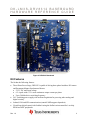
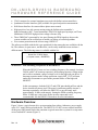
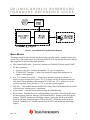
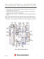
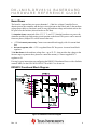
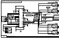
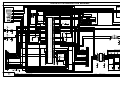
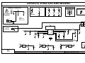
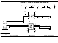
DK-LM3S-DRV8312 BASEBOARD
HARDWARE REFERENCE GUIDE
Medium Voltage Digital Motor Control Kit for Stellaris®
Microcontrollers (DK-LM3S-DRV8312)
The Medium Voltage Digital Motor Control (DMC) kit (DK-LM3S-DRV8312), shown in
Figure 1, provides a great way to learn and experiment with digital control of medium
voltage brushless motors to increase efficiency of operation. This document describes the
DRV8312 hardware, and explains the functions and locations of jumpers and connectors
present on the board.
Figure 1. DK-LM3S-DRV8312 Kit (Stellaris® Version)
WARNING
This EVM is meant to be operated in a lab environment only and is not considered by
Texas Instruments to be a finished end-product fit for general consumer use
This EVM must be used only by qualified engineers and technicians familiar with risks
associated with handling high-voltage electrical and mechanical components, systems,
and subsystems.
This equipment may be operated at voltages and currents that can result in electrical shock, fire
hazard and/or personal injury if not properly handled or applied. Equipment must be used with
necessary caution and appropriate safeguards employed to avoid personal injury or property damage.
It is the user’s responsibility to confirm that the voltages and isolation requirements are identified and
understood, prior to powering the board and or simulation. If powered with a supply other than the one
included in the kit, do not touch the EVM or components connected to the EVM.
Rev. 1.0
1
DK-LM3S-DRV8312 BASEBOARD
HARDWARE REFERENCE GUIDE
Figure 2. DRV8312 Baseboard
Kit Features
The kit has the following features
•
•
•
•
Three-Phase Power Stage, DRV8312 capable of driving three-phase brushless DC motors
and Permanent Magnet Synchronous Motors
• 52.5 V DC max input voltage
• 6.5 A peak with a 3.5 A max continuous output current per phase
• Up to 500 khz driver switching frequency
24 V switching power supply with on-board regulation for powering other analog and
digital circuitry
Isolated CAN and SPI communication (controlCARD support-dependent)
Closed-loop digital control with feedback using the Stellaris microcontroller’s on-chip
PWM and ADC peripherals
Rev. 1.0
2
DK-LM3S-DRV8312 BASEBOARD
HARDWARE REFERENCE GUIDE
•
•
•
•
•
•
JTAG connector for external emulators (not used with Stellaris microcontrollers)
Quadrature Encoder Interface (QEI) available for speed and position measurement
Hall-Sensor Interface for sensored three-phase motor control
High precision, low-side current sensing using the Stellaris microcontroller’s
high-performance ADC, Texas Instruments’ OPA365A high-speed op-amps, and Texas
Instruments’ REF3025 high precision voltage reference chip
Three PWM DACs generated by low-pass filtering the PWM signals to observe the
system variables on an oscilloscope to enable easy debug of control algorithms
Over-current protection on the inverter stage, DRV8312
The software available with the kit is pre-optimized for the motors that are available with the
kit. The software is open source, and therefore, can be easily modified to tune and run a
different motor. The following motor is available with the kit:
Nema Size 17 BLDC Motor
(11A peak current , 4000RPM)
WARNING: Low-Switching Frequencies on the DRV8312
When the DRV8312 runs at a low switching frequency (for example, less than
20 kHz with 47 nF bootstrap capacitor), the bootstrap capacitor voltage might
not be able to maintain a proper voltage level for the high-side gate driver. A
bootstrap capacitor under voltage protection circuit (BST_UVP) will start
under this circumstance to prevent the potential failure of the high-side
MOSFET.
In this circumstance, both the FAULT and OTW pins should pull low and the
device should self-protect itself. The motor’s inductance and the inverter’s
bootstrap capacitance will allow the DRV8312 to run efficiently until
approximately 10 kHz (with margin). Setting the PWM switching frequency
below 10 kHz may cause issues on the inverter output and is not
recommended. See the DRV8312 data sheet for more information.
Hardware Overview
Figure 3 shows a typical motor drive system running from either a laboratory power supply
or the 24 V supply delivered with the kit. The DRV8312-C2-KIT’s motor control board has
all the power and control blocks that constitute a typical motor drive system for a step motor
or two brushed DC motors (Figure 5).
Rev. 1.0
3
DK-LM3S-DRV8312 BASEBOARD
HARDWARE REFERENCE GUIDE
Figure 3. Typical Motor Drive System Block Diagram
Macro Blocks
The motor control board is divided into functional groups that enable a complete motor drive
system. These functional groups are called macro blocks. This list describes the macro blocks
that are present on the board and their functions::
•
•
•
•
•
•
ISO controlCARD socket – Socket for a Stellaris or C2000 MCU-based controlCARD
DC Bus Connection
• J9 power entry jack - Connect the supplied +24 V power supply here
• “PVDD/GND” Terminals – Connect an external lab supply here making sure to
observe correct polarity
Aux-12 V Control Power Entry – Connectors to optionally provide an external 12 V
supply for logic and gate drive power. The 12 V supply can also be regulated on-board
from the DC bus depending on the setting of JP1. Set to the “VR1” position to use the
on-board regulator. Set to position “+12 V” to use the external regulator.
DRV8312 – This module includes the DRV8312 Three-Phase PWM Motor Driver and all
of the necessary external passive components.
Current Sense – Low-side shunt current sensing on each half-bridge.
Reset Switch – Individual reset for each half-bridge. Reset can be forced manually from
the three-position switch or through a GPIO from the MCU. Setting switch in the down
position, “RESET” disables the half-bridge outputs. Setting the switch in the middle
position will allow control through a GPIO on the MCU. Setting the switch in the up
position, “NORMAL OP” disables control from the MCU and enables the half-bridge
outputs.
Rev. 1.0
4
DK-LM3S-DRV8312 BASEBOARD
HARDWARE REFERENCE GUIDE
•
•
•
Mode Jumper “M1” – DRV8312 mode can be set to select between cycle-by-cycle
current limit or latched over-current.
Quadrature Encoder Connections – Connections are available for an optional shaft
encoder to interface to the MCU’s QEP peripheral.
Hall Effect Sensor Connections – Connections are available for optional Hall Effect
Sensors.
Figure 4 shows the position of the macro blocks on the board. All the PWMs and ADC
signals which are the actuation and sense signals have designated test points on the board,
which makes it easy for an application developer to try out new algorithms and strategies.
Figure 4. DRV8312-EVM Board Macros
Rev. 1.0
5
DK-LM3S-DRV8312 BASEBOARD
HARDWARE REFERENCE GUIDE
Board Power
The board is separated into two power domains*: (1)the low voltage Controller Power
domain powers the controller and the logic circuit present on the board, and (2) the medium
voltage power delivery line that is used to carry the medium voltage and current such as the
DC power for the Inverter (also referred to as DC Bus).
1) Controller Power comprised of the 12 V, 5 V, and 3.3 V that the board uses to power the
controller and the logic and sensing circuit present on the board. This power can be sourced
from two places (Jumper JP1 selects between the two):
•
•
+12V DC control power entry: Connect an external bench supply with 1A current limit
here
On board regulator, VR1: +12V is regulated from DC bus power via an on-board buck
regulator
2) DC Bus Power is the medium voltage line – up to 52.5V - that provides the voltage to the
inverter stage to generate three phases to control the motor(s). Connect supplied 24 V
regulator to J9.
For step-by-step instructions on configuring the DRV8312 baseboard for use with a Stellaris
controlCARD, see the DK-LM3S-DRV8312 Read Me First document.
DRV8312 Functional Block Diagram
Figure 5. DRV8312 Functional Diagram
Rev. 1.0
6
DK-LM3S-DRV8312 BASEBOARD
HARDWARE REFERENCE GUIDE
References
In addition to this document, the following references are included on the Stellaris
controlCARD Development Kit CD and are also available for download at
www.ti.com/stellaris:
• Stellaris® LM3S818 controlCARD Module (MDL-LM3S818CNCD) README First,
publication MDL-LM3S818CNCD-RMF
• Stellaris® LM3S818 controlCARD Module (MDL-LM3S818CNCD) User’s Manual,
publication MDL-LM3S818CNCD-UM
• Stellaris® Development and Evaluation Kits for Code Composer Studio™ Quickstart
Guide
• Stellaris® LM3S818 Microcontroller Data Sheet, publication DS-LM3S818
• StellarisWare Driver Library
• StellarisWare Driver Library User’s Manual, publication SW-DRL-UG
• Stellaris® DK-LM3S-DRV8312 InstaSPIN™-BLDC README First, publication
DK-LM3S-DRV8312-RMF
• Medium Voltage Digital Motor Control Kit for Stellaris® Microcontrollers
(DK-LM3S-DRV8312) Baseboard Hardware Reference Guide, publication
DK-LM3S-DRV8312-RG
• Three-Phase PWM Motor Driver (DRV8312) Data Sheet, publication SLES256
• Sensorless Trapezoidal Control of BLDC Motors Using BEMF Integration
(InstaSPIN™-BLDC) on Stellaris® Microcontrollers Application Note, publication
AN01289
Additional references include:
• The GUI and corresponding Stellaris code were developed by D3 Engineering. The GUI
was created using Crosshairs Interface Designer from Crosshairs Embedded. There are
links to each of the companies’ web sites within the GUI. There is also information for
downloading Crosshairs Interface Designer so that you can modify the GUI that comes
with this kit. The More… tab gives a brief overview of the Interface Designer software.
• Crosshairs Embedded: www.crosshairsembedded.com
• D3 Engineering: www.d3engineering.com
Schematics
This section contains the schematics for the DK-LM3S-DRV8312 evaluation board:
•
•
•
•
DRV8312 Evaluation Board (sheets 1 and 2)
Power Inputs and Supplies (sheet 3)
Isolation Circuit (sheet 4)
Revision History (sheet 5)
Rev. 1.0
7
DRV8312 EVALUATION BOARD
R49
+2.5V
C20
R19
V2+
+3.3V
28.7000Kohms
C24
220.0000pF
33.0000ohms
0.1000uF
IS-IhbC
R29
GND
1.0000Kohms
C58
R41
0.0010uF
GND
OA2
+IN
V+
VOUT
C26
IS-TOTAL
3
49.9000Kohms
4
220.0000pF
V-
R21
1
IC-FB
2
0.0000ohms
OPA365AIDBV
GVDD
R33
C12
-IN
TO J1
5
IC-FB
GND
1.0000Kohms
R25
0.1000uF
19.1000Kohms
STUFF OPTION
R48
GND
1
GVDD
U1
43
C30
2
GVDD
+
C31
C32
47.0000uF
1.0000uF
C36
C37
0.1000uF
0.1000uF
C57
3
4
OUT_C
220.0000pF
L2
R50
10.0000mohms
3
FROM J1
1
2
RSTC
M1
3
2
RSTB
3
RESET_C~
1
R51
35
9
33
R53
32
12
R36
PWM_B
IS-IhbB
PVDD
0.0470uF
13
0.1000uF
I-TOTAL
GND
R24
HIGH VOLTAGE WARNING
FOR VOLTAGE POTENTIALS OF
50V OR GREATER
OUTPUTS
ADC-Vhb2
95.3000Kohms
R43
C56
4.9900Kohms
0.0470uF
GND
R52
TO J1
MOTOR
MOC
1
MOB
GND
2
MOA
3
10.0000mohms
RESET_A~
GND
R37
PWM_A
GND
31
14
OUT_B
4.7000uH
15
PWMB
IS-IhbB
29
IS-IhbA
28
16
/FAULT
4.9900Kohms
0.0470uF
GND
TO J1
GND
R55
GND
+2.5V
C22
33.0000ohms
0.1000uF
GND
0.1000uF
C60
25
21
24
22
R62
0.0010uF
GND
GND
IS-TOTAL
23
3
49.9000Kohms
4
220.0000pF
DRV8312DDW
OA4
+IN
-IN
2
IB-FB
GND
R27
R54
GVDD
+2.5V
1.0000uF
Q2
C21
U1
33.0000ohms
220.0000pF
+3.3V
0.1000uF
R30
GND
1.0000Kohms
GND
R47
C59
392.0000ohms
R63
V3+
28.7000Kohms
C29
IS-IhbA
PowerPad
+3.3V
ZXM62P03E6TA
ZXM62P03E6TA
IB-FB
0.0000ohms
STUFF OPTION
GND
GND
LED6
R23
1
19.1000Kohms
R46
C35
D
TO J1
5
OPA365AIDBV
R34
392.0000ohms
S
V-
1.0000Kohms
+3.3V
ZXM62P03E6TA
G
V+
VOUT
C28
1.0000uF
LED5
+3.3V
R31
1.0000Kohms
ZXM62P03E6TA
D
R64
V4+
28.7000Kohms
C39
IS-IhbB
C46
C45
0.1000uF
20
S
C55
220.0000pF
PVDD
19
G
L4
OUT_A
26
18
C34
ADC-Vhb1
R45
27
PWMA
Q1
4
R44
4.7000uH
17
GVDD
IS-IhbA
95.3000Kohms
30
OUT_A
/OTW
L3
OUT_B
30.0000Kohms
FAULT~
I-TOTAL
0.0000ohms
2
TO J1
GND
R42
IS-TOTAL
C43
C42
0.1000uF
1.0000ohms
OTW~
4.9900Kohms
GND
IS-TOTAL
10.0000mohms
0.1000uF
AGND
C50
GND
C33
RESET_B~
R20
1
IS-TOTAL
11
2
RSTA
R39
5.0000mohms
34
10
VREG
Shielded GND
GND
8
M1
PBC03SAAN
PWM_C
ROUTED GROUND
(SHIELDED FROM GND PLANE)
36
1
2
ADC-Vhb3
95.3000Kohms
37
V-
TO J1
5
38.3000Kohms
R38
7
V+
-IN
1.0000Kohms
IS-IhbC
IS-TOTAL
IS-IhbC
OA1
+IN
OPA365AIDBV
R32
6
1
4
4.7000uH
38
3
VOUT
OUT_C
GND
5
GND
49.9000Kohms
C25
Shielded GND
GND
PWMC
3
R40
0.0010uF
GND
39
GND
R28
1.0000Kohms
PVDD
40
+3.3V
C23
0.1000uF
IS-TOTAL
41
GND
33.0000ohms
57.6000Kohms
220.0000pF
42
1.0000uF
R18
V1+
+2.5V
C19
44
R16
GND
0.0010uF
GND
GND
IS-TOTAL
3
49.9000Kohms
OA3
+IN
V+
VOUT
C27
4
220.0000pF
R35
1.0000Kohms
-IN
V-
TO J1
5
R22
1
IA-FB
0.0000ohms
2
OPA365AIDBV
IA-FB
GND
R26
19.1000Kohms
TI
PAGE INFO:
DRV8312 EVALUATION BOARD
DESIGN LEAD RYAN KEHR
EDGE # 6517813
DATE
MARCH 23, 2011
FILENAME DRV8312EVM_RevD
SCH REV
C
PCB REV
D
SHEET 1 OF 6
DRAWN BY
LDN
DRV8312 EVALUATION BOARD
TO ISOLATION CIRCUIT
FROM U1
SPI-SOMI
ADC-Vhb1
SPI-STE
ADC-Vhb2
CAN-TX
J6
ADC-Vhb3
1
CAN-RX
2
3
I-TOTAL
100
GND
99
IC-FB
98
IB-FB
+5V
97
+5VD
JP2
IA-FB
96
PBC02SAAN
95
94
CAN-TX
93
92
91
QEPI
+3.3V
R70
QEPB
90
SPI-STE
89
88
SPI-SOMI
4.9900Kohms
JP3
1
PBC02SAAN
87
2
86
C70
TL1015AF160QG
START
CAP2
85
FAULT~
84
OTW~
83
0.1000uF
GND
GND
82
+3.3V
81
R71
80
4.9900Kohms
JP5
DAC2
1
R14
PBC02SAAN
470.0000ohms
2
C17
C71
TL1015AF160QG
STOP
DAC_PWM2
79
START
78
77
0.4700uF
0.1000uF
GND
GND
GND
STOP
76
RESET_C~
75
74
RESET_B~
73
RESET_A~
72
71
ADC-Vhb2
70
69
68
67
IC-FB
66
65
J5
1
64
+5VD
63
3
QEPI
5
62
QEPB
7
61
I-TOTAL
60
9
CAP2
11
59
IA-FB
13
58
15
57
DAC_PWM2
17
56
19
55
21
54
23
53
PWM_B
25
52
51
27
I-TOTAL
29
GND
VDCBUS
33
J1
EMU0
EMU1
TRSTn
TMS
TDO
TCK
TDI
DGND
+5V IN
GPIO-34
GPIO-33
GPIO-32
GPIO-31
GPIO-30
GPIO-29
GPIO-28
+5V IN
GPIO-87
GPIO-23
GPIO-22
GPIO-21
GPIO-20
GPIO-19
GPIO-18
GPIO-17
GPIO-16
+5V IN
DGND
GPIO-27
GPIO-26
GPIO-25
GPIO-24
GPIO-14
GPIO-15
GPIO-13
GPIO-12
+5V IN
GPIO-86
GPIO-85
GPIO-84
GPIO-49
GPIO-48
GPIO-11
GPIO-10
GPIO-09
GPIO-08
+5V IN
GPIO-07
DGND
GPIO-06
GPIO-05
GPIO-04
GPIO-03
GPIO-02
GPIO-01
GPIO-63
GPIO-00
GPIO-62
ADC-A7
ADC-B7
GPIO-61
GPIO-60
ADC-A6
ADC-B6
GPIO-59
GPIO-50
ADC-A5
NC
ADC-A4
AGND
ADC-A3
AGND
ADC-A2
AGND
ADC-A1
AGND
ADC-A0
GND-ISO
ADC-B5
NC
ADC-B4
AGND
ADC-B3
AGND
ADC-B2
AGND
ADC-B1
AGND
ADC-B0
GND-ISO
NC
NC
NC
NC
NC
NC
NC
NC
V33-ISO
V33-ISO
50
+3.3V
49
48
47
46
45
44
43
4
5
6
7
8
9
10
11
12
13
14
GPIO-28
470.0000ohms
TO U1
J12
PBC02SAAN
42
GND
41
STATUS
40
QEPA
39
SPI-CLK
38
SPI-SIMO
37
36
CAP3
35
CAP1
34
LED-2
33
R15
LED-1
C18
32
31
0.4700uF
30
BUF1
1
GND
29
DAC_PWM1
R65
28
DAC_PWM3
470.0000ohms
2
DAC3
3
C40
27
1A
GND
1Y
VCC
2Y
2A
R72
6
330.0000ohms
5
+3.3V
R73
4
330.0000ohms
SN74LVC2G17DBV
0.4700uF
26
25
DAC1
470.0000ohms
GND
PWM_C
24
PWM_B
23
PWM_A
LED10
+3.3V
LED11
GND
C73
GND
GND
0.1000uF
22
21
ADC-Vhb1
GND
20
19
+5VD
18
17
4
16
15
6
ADC-Vhb3
STATUS
14
STUFF OPTION
8
QEPA
10
13
+5VD
12
12
CAP3
11
TACH/SPEED
INPUT
10
9
CAP1
+3.3V
8
7
J5
2
IB-FB
DAC_PWM1
R66
TSI
10.0000Kohms
6
DAC_PWM3
PWM_A
5
GND
PWM_C
+3.3V
1
16
E1A
18
3
14
E1B
20
4
13
22
5
12
E2A
24
6
11
E2B
26
7
10
E2C
8
+3.3V
IC-FB
2
1
C72
ADC-Vhb2
1.0000uF
ADC-Vhb1
GND
15
R58
R59
R60
R61
1.0000Kohms
1.0000Kohms
1.0000Kohms 1.0000Kohms
ENCODER
1
2
E1C
3 J4
4
+5VD
5
GND
9
CAP
TXB0106PW
32
34
R57
1.0000Kohms 1.0000Kohms
2
16
30
3
U2
R56
+5VD
14
28
4
GND
1
+3.3V
+5VD
2
36
TSI
38
C41
40
VDCBUS
3 J10
C44
0.1000uF
0.1000uF
C47
C49
0.0010uF
C52
0.0010uF
+5VD
4
5
0.0010uF
GND
GND
GND
IA-FB
37
3
SPI-SIMO
STATUS
R17
IB-FB
35
2
GND
CAN-RX
GND
ADC-Vhb3
31
SPI-CLK
JTAG
1
4
GND
C48
C51
C54
0.0010uF
0.0010uF
0.0010uF
39
GND
PVDD
R12
R13
95.3000Kohms
4.9900Kohms
GND
GND
TI
PAGE INFO:
DRV8312 EVALUATION BOARD
DESIGN LEAD RYAN KEHR
EDGE # 6517813
MARCH 23, 2011
DATE
FILENAME DRV8312EVM_RevD
SCH REV
C
PCB REV
D
SHEET 2 OF 6
DRAWN BY
LDN
DRV8312 EVALUATION BOARD
MAIN POWER IN
PVDD
PVDD
GVDD
BOM ONLY
+5VD
STANDOFFS
R1
C2
PVDD
PVDDIN
PVDD
0.1000uF
LED1
3.3000ohms
LED2
GROUND TESTPOINTS
LED3
1
+
HIGH
VOLTAGE
WARNING
2
+
C1
C11
C3
GND
470.0000uF
470.0000uF
EMI
SNUBBER
GND
GND
GND
R2
4.9900Kohms
0.0100uF
R3
SHIELD
SIGNAL
R4
2.4900Kohms
GND
GND
GND
GND
J9
SHUNT
4.9900Kohms
GND
GND
PVDD
NOM = 50V
MAX = 52.5V
3
1
2
PBC03SAAN
3
GVDD
GND
JP1
2
JP1
1-2: GVDD = VR1
2-3: GVDD = AUX 12V
1
C7
0.1000uF
PBC02SAAN
EXTERNAL
12V INPUT
AUX-12V
1
2
1
GND
2
PVDD
+
3
C4
C5
R5
22.0000uF
0.0150uF
348.0000Kohms
4
5
GND
GND
C6
R7
33.2000Kohms
0.0150uF
205.0000Kohms
GND
PH
VIN
10
SS/TR
VSENSE
RT/CLK
PWRGD
R10
CR1
8
COMP
EN
39.0000uH
9
GND
30BQ100
+
C10
10.0000Kohms
GND
7
100.0000uF
R8
6
442.0000Kohms
R11
GND
TPS54160DGQ
R6
GND
L1
VR1
BOOT
C8
C9
180.0000pF
12.0000pF
GND
681.0000ohms
GND
VR1
PowerPad
GND
GND
GND
R9
GND
10.0000Kohms
USER POWER ACCESS
GVDD
1
2
GVDD
VR2
VIN
VOUT
GND
+5V
3
+
UA78M05CDCY
GND
1
2
C14
C13
47.0000uF
0.1000uF
+3.3V
VR3
VIN
VOUT
GND
1
3
+
TL1963A-33DCY
GND
VR4
+3.3V
C16
C15
0.4700uF
47.0000uF
3
C38
0.1000uF
VIN
VOUT
+2.5V
2
REF3025AIDBZ
TI
GND
PAGE INFO:
POWER INPUTS AND SUPPLIES
DESIGN LEAD RYAN KEHR
GND
EDGE # 6517813
1
2
GND
GND
J2
+3.3V
1
2
PBC02SAAN
J3
PBC02SAAN
GND
GND
GND
GND
+5V
GND
DATE
MARCH 23, 2011
FILENAME DRV8312EVM_RevD
SCH REV
C
PCB REV
D
SHEET 3 OF 6
DRAWN BY LDN
DRV8312 EVALUATION BOARD
R100
U3
1
+5V
+VI
1.0000ohms
C100
2
-VI
1.0000uF
7
+VO
1
+5VI
5
C103
3
4
2.2000uF
DCH010505S
GND
+3.3VD
2
C101
5
-VO
VR5
2.2000uF
IGND
IGND
GND
TPS73633MDBVREP
C102
IGND
0.1000uF
IGND
IGND
+3.3V
C104
C105
0.1000uF
1.0000uF
GND
1
2
3
4
IGND
U4
VCC1
VCC2
RXD
CANH
TXD
CANL
GND1
GND2
8
J7
7
CAN-H
1
6
CAN-L
2
5
R101
ISO1050DUB
GND
120.0000ohms
3
JP4
PBC03SAAN
PBC02SAAN
IGND
IGND
C108
0.1000uF
CAN-RX
GND
IGND
CAN-TX
TO J1
9
GND
10
+3.3V
11
SPI-SOMI
12
SPI-SIMO
13
14
SPI-CLK
15
GND
SPI-STE
16
U5
GND2
GND1
EN2
EN1
IND
OUTD
OUTC
INC
OUTB
INB
OUTA
INA
GND2
GND1
VCC2
VCC1
8
IGND
7
+3.3VD
6
iSD-I
5
iSD-O
iSD-O
1
4
iCLK-O
iCLK-O
2
3
iGPIO
iSD-I
3
iGPIO
4
2
IGND
J8
1
5
ISO7241ADW
+3.3V
+3.3VD
C106
0.1000uF
GND
TI
PAGE INFO:
ISOLATION CIRCUIT
DESIGN LEAD RYAN KEHR
IGND
C107
0.1000uF
IGND
EDGE # 6517813
DATE
MARCH 23, 2011
FILENAME DRV8312EVM_RevD
SCH REV
C
PCB REV
D
SHEET 4 OF 6
DRAWN BY LDN
DRV8312 EVALUATION BOARD
REVISION HISTORY
REVISION DESCRIPTION
TI
DATE
A
INITIAL RELEASE
B
1. DELETED OUTA, OUTB, OUTC.
2. ADDED OUTPUT CONNECTOR, TITLED MOTOR.
3. CONNECTED L2-2, L3-2 AND L4-2 TO MOTOR-1,2 AND 3, RESPECTIVELY.
4. DELETED PVDD, GND, +12V AND GND(GND2).
5. ADDED POWER CONNECTOR, VIN.
6. CONNECTED VIN-4 TO C1-1.
7. CONNECTED VIN-2,3 TO GND.
8. CONNECTED VIN-1 TO +12V.
9. ADDED TESTPOINTS TO IA-FB, IB-FB, IC-FB AND I-TOTAL.
10. ADDED 2 PIN HEADERS J2 AND J3 FOR USER POWER ACCESS.
11. CONNECTED J2-1,2 TO +5V AND GND.
12. CONNECTED J3-1,2 TO +3.3V AND GND.
13. COMBINED ENCODER AND CAP INTO ONE 2x5 HEADER, TITLED J4.
14. ADDED 3 PIN HEADER, JP3, LABELED TACH/SPEED INPUT.
15. CONNECTED JP3-1,2,3 TO +3.3V, J1-7 AND GND, RESPECTIVELY.
16. RENAMED S1 TO RSTA.
17. SWAPPED U1-29 AND U1-30.
18. ADDED 40 PIN HEADER, J5 AND CONNECTED PINS TO ACTIVE PINS OF J1.
19. ADDED SWITCHES, S1 AND S2 TO U1-76 AND U1-78.
20. COPIED DAC1 CIRCUIT, CALLED DAC3, AND CONNECTED TO J1-28.
21. CHANGED R24-R27 TO 33.0K OHMS.
22. CHANGED R28-R35, R56-R61 TO 1.00K OHMS.
23. CHANGED R48, R49, R54 AND R55 TO 49.9K OHMS.
24. ADDED ISOLATION CIRCUITS.
25. ADDED 12V CONNECTOR, J9.
26. CHANGED C4 TO 22UFD/100V.
27. CHANGED C5 AND C6 TO 100V.
PAGE INFO:
REVISION HISTORY
DESIGN LEAD RYAN KEHR
EDGE # 6517813
APPROVAL
MAY 4, 2010
ML
MARCH 23, 2011
RK
DATE
MARCH 23, 2011
FILENAME DRV8312EVM_RevD
SCH REV
C
PCB REV
D
SHEET 5 OF 6
DRAWN BY LDN
DK-LM3S-DRV8312 BASEBOARD
HARDWARE REFERENCE GUIDE
SCHEMATIC DISCLAIMER AND WARNINGS
TI provides the schematic drawings to help users develop DRV8312 & Stellaris MCU
based reference design products. Application safety, safety of the Medium Voltage DMC
kit and design integrity of such reference designs are solely responsibility of the user.
Any reference designs generated off these schematics must take into account necessary
product safety design requirements, including interface components and load motors in
order to avoid user risks including potential for fire hazard, electrical shock hazard and
personal injury, including considerations for anticipated agency certification compliance
requirements.
Such product safety design criteria shall include but not be limited to critical circuit
creepages and clearances, component selection, ratings compatibility of controlled motor
loads, and required protective means (ie output fusing) depending on the specific loads
being controlled.
TI accepts no responsibility for design integrity of any reference designs based on
supplied schematic drawings and the schematics are strictly for development purposes.
EVALUATION BOARD/KIT IMPORTANT NOTICE
Texas Instruments (TI) provides the enclosed product(s) under the following conditions:
This evaluation board/kit is intended for use for ENGINEERING DEVELOPMENT,
DEMONSTRATION, OR EVALUATION PURPOSES ONLY and is not considered by TI
to be a finished end-product fit for general consumer use. Persons handling the
product(s) must have electronics training and observe good engineering practice
standards. As such, the goods being provided are not intended to be complete in terms
of required design-, marketing-, and/or manufacturing-related protective considerations,
including product safety and environmental measures typically found in end products
that incorporate such semiconductor components or circuit boards. This evaluation
board/kit does not fall within the scope of the European Union directives regarding
electromagnetic compatibility, restricted substances (RoHS), recycling (WEEE), FCC, CE
or UL, and therefore may not meet the technical requirements of these directives or
other related directives.
Should this evaluation board/kit not meet the specifications indicated in the User’s
Guide, the board/kit may be returned within 30 days from the date of delivery for a full
refund. THE FOREGOING WARRANTY IS THE EXCLUSIVE WARRANTY MADE BY SELLER
TO BUYER AND IS IN LIEU OF ALL OTHER WARRANTIES, EXPRESSED, IMPLIED, OR
STATUTORY, INCLUDING ANY WARRANTY OF MERCHANTABILITY OR FITNESS FOR ANY
PARTICULAR PURPOSE.
The user assumes all responsibility and liability for proper and safe handling of the
goods. Further, the user indemnifies TI from all claims arising from the handling or use
of the goods. Due to the open construction of the product, it is the user’s responsibility
to take any and all appropriate precautions with regard to electrostatic discharge.
EXCEPT TO THE EXTENT OF THE INDEMNITY SET FORTH ABOVE, NEITHER PARTY SHALL
BE LIABLE TO THE OTHER FOR ANY INDIRECT, SPECIAL, INCIDENTAL, OR
CONSEQUENTIAL DAMAGES.
TI currently deals with a variety of customers for products, and therefore our
arrangement with the user is not exclusive.
Rev. 1.0
13
DK-LM3S-DRV8312 BASEBOARD
HARDWARE REFERENCE GUIDE
TI assumes no liability for applications assistance, customer product design,
software performance, or infringement of patents or services described herein.
Please read the User’s Guide and, specifically, the Warnings and Restrictions notice in
the User’s Guide prior to handling the product. This notice contains important safety
information about temperatures and voltages. For additional information on TI’s
environmental and/or safety programs, please contact the TI application engineer or
visit www.ti.com/esh.
No license is granted under any patent right or other intellectual property right of TI
covering or relating to any machine, process, or combination in which such TI products
or services might be or are used.
Mailing Address:
Texas Instruments
Post Office Box 655303
Dallas, Texas 75265
Copyright © 2010, Texas Instruments Incorporated
FCC Warning
This evaluation board/kit is intended for use for ENGINEERING DEVELOPMENT,
DEMONSTRATION, OR EVALUATION PURPOSES ONLY and is not considered by TI
to be a finished end-product fit for general consumer use. It generates, uses, and can
radiate radio frequency energy and has not been tested for compliance with the limits of
computing devices pursuant to part 15 of FCC rules, which are designed to provide
reasonable protection against radio frequency interference. Operation of this equipment
in other environments may cause interference with radio communications, in which case
the user at his own expense will be required to take whatever measures may be
required to correct this interference.
Copyright © 2011 Texas Instruments, Inc. All rights reserved. Stellaris and StellarisWare are registered trademarks of Texas
Instruments. ARM and Thumb are registered trademarks, and Cortex is a trademark of ARM Limited. Other names and
brands may be claimed as the property of others.
Texas Instruments
108 Wild Basin Rd., Suite 350
Austin, TX 78746
http://www.ti.com/stellaris
Rev. 1.0
11/17/2011
EVALUATION BOARD/KIT/MODULE (EVM) ADDITIONAL TERMS
Texas Instruments (TI) provides the enclosed Evaluation Board/Kit/Module (EVM) under the following conditions:
The user assumes all responsibility and liability for proper and safe handling of the goods. Further, the user indemnifies TI from all claims
arising from the handling or use of the goods.
Should this evaluation board/kit not meet the specifications indicated in the User’s Guide, the board/kit may be returned within 30 days from
the date of delivery for a full refund. THE FOREGOING LIMITED WARRANTY IS THE EXCLUSIVE WARRANTY MADE BY SELLER TO
BUYER AND IS IN LIEU OF ALL OTHER WARRANTIES, EXPRESSED, IMPLIED, OR STATUTORY, INCLUDING ANY WARRANTY OF
MERCHANTABILITY OR FITNESS FOR ANY PARTICULAR PURPOSE. EXCEPT TO THE EXTENT OF THE INDEMNITY SET FORTH
ABOVE, NEITHER PARTY SHALL BE LIABLE TO THE OTHER FOR ANY INDIRECT, SPECIAL, INCIDENTAL, OR CONSEQUENTIAL
DAMAGES.
Please read the User's Guide and, specifically, the Warnings and Restrictions notice in the User's Guide prior to handling the product. This
notice contains important safety information about temperatures and voltages. For additional information on TI's environmental and/or safety
programs, please visit www.ti.com/esh or contact TI.
No license is granted under any patent right or other intellectual property right of TI covering or relating to any machine, process, or
combination in which such TI products or services might be or are used. TI currently deals with a variety of customers for products, and
therefore our arrangement with the user is not exclusive. TI assumes no liability for applications assistance, customer product design,
software performance, or infringement of patents or services described herein.
REGULATORY COMPLIANCE INFORMATION
As noted in the EVM User’s Guide and/or EVM itself, this EVM and/or accompanying hardware may or may not be subject to the Federal
Communications Commission (FCC) and Industry Canada (IC) rules.
For EVMs not subject to the above rules, this evaluation board/kit/module is intended for use for ENGINEERING DEVELOPMENT,
DEMONSTRATION OR EVALUATION PURPOSES ONLY and is not considered by TI to be a finished end product fit for general consumer
use. It generates, uses, and can radiate radio frequency energy and has not been tested for compliance with the limits of computing
devices pursuant to part 15 of FCC or ICES-003 rules, which are designed to provide reasonable protection against radio frequency
interference. Operation of the equipment may cause interference with radio communications, in which case the user at his own expense will
be required to take whatever measures may be required to correct this interference.
General Statement for EVMs including a radio
User Power/Frequency Use Obligations: This radio is intended for development/professional use only in legally allocated frequency and
power limits. Any use of radio frequencies and/or power availability of this EVM and its development application(s) must comply with local
laws governing radio spectrum allocation and power limits for this evaluation module. It is the user’s sole responsibility to only operate this
radio in legally acceptable frequency space and within legally mandated power limitations. Any exceptions to this are strictly prohibited and
unauthorized by Texas Instruments unless user has obtained appropriate experimental/development licenses from local regulatory
authorities, which is responsibility of user including its acceptable authorization.
For EVMs annotated as FCC – FEDERAL COMMUNICATIONS COMMISSION Part 15 Compliant
Caution
This device complies with part 15 of the FCC Rules. Operation is subject to the following two conditions: (1) This device may not cause
harmful interference, and (2) this device must accept any interference received, including interference that may cause undesired operation.
Changes or modifications not expressly approved by the party responsible for compliance could void the user's authority to operate the
equipment.
FCC Interference Statement for Class A EVM devices
This equipment has been tested and found to comply with the limits for a Class A digital device, pursuant to part 15 of the FCC Rules.
These limits are designed to provide reasonable protection against harmful interference when the equipment is operated in a commercial
environment. This equipment generates, uses, and can radiate radio frequency energy and, if not installed and used in accordance with the
instruction manual, may cause harmful interference to radio communications. Operation of this equipment in a residential area is likely to
cause harmful interference in which case the user will be required to correct the interference at his own expense.
FCC Interference Statement for Class B EVM devices
This equipment has been tested and found to comply with the limits for a Class B digital device, pursuant to part 15 of the FCC Rules.
These limits are designed to provide reasonable protection against harmful interference in a residential installation. This equipment
generates, uses and can radiate radio frequency energy and, if not installed and used in accordance with the instructions, may cause
harmful interference to radio communications. However, there is no guarantee that interference will not occur in a particular installation. If
this equipment does cause harmful interference to radio or television reception, which can be determined by turning the equipment off and
on, the user is encouraged to try to correct the interference by one or more of the following measures:
• Reorient or relocate the receiving antenna.
• Increase the separation between the equipment and receiver.
• Connect the equipment into an outlet on a circuit different from that to which the receiver is connected.
• Consult the dealer or an experienced radio/TV technician for help.
For EVMs annotated as IC – INDUSTRY CANADA Compliant
This Class A or B digital apparatus complies with Canadian ICES-003.
Changes or modifications not expressly approved by the party responsible for compliance could void the user’s authority to operate the
equipment.
Concerning EVMs including radio transmitters
This device complies with Industry Canada licence-exempt RSS standard(s). Operation is subject to the following two conditions: (1) this
device may not cause interference, and (2) this device must accept any interference, including interference that may cause undesired
operation of the device.
Concerning EVMs including detachable antennas
Under Industry Canada regulations, this radio transmitter may only operate using an antenna of a type and maximum (or lesser) gain
approved for the transmitter by Industry Canada. To reduce potential radio interference to other users, the antenna type and its gain should
be so chosen that the equivalent isotropically radiated power (e.i.r.p.) is not more than that necessary for successful communication.
This radio transmitter has been approved by Industry Canada to operate with the antenna types listed in the user guide with the maximum
permissible gain and required antenna impedance for each antenna type indicated. Antenna types not included in this list, having a gain
greater than the maximum gain indicated for that type, are strictly prohibited for use with this device.
Cet appareil numérique de la classe A ou B est conforme à la norme NMB-003 du Canada.
Les changements ou les modifications pas expressément approuvés par la partie responsable de la conformité ont pu vider l’autorité de
l'utilisateur pour actionner l'équipement.
Concernant les EVMs avec appareils radio
Le présent appareil est conforme aux CNR d'Industrie Canada applicables aux appareils radio exempts de licence. L'exploitation est
autorisée aux deux conditions suivantes : (1) l'appareil ne doit pas produire de brouillage, et (2) l'utilisateur de l'appareil doit accepter tout
brouillage radioélectrique subi, même si le brouillage est susceptible d'en compromettre le fonctionnement.
Concernant les EVMs avec antennes détachables
Conformément à la réglementation d'Industrie Canada, le présent émetteur radio peut fonctionner avec une antenne d'un type et d'un gain
maximal (ou inférieur) approuvé pour l'émetteur par Industrie Canada. Dans le but de réduire les risques de brouillage radioélectrique à
l'intention des autres utilisateurs, il faut choisir le type d'antenne et son gain de sorte que la puissance isotrope rayonnée équivalente
(p.i.r.e.) ne dépasse pas l'intensité nécessaire à l'établissement d'une communication satisfaisante.
Le présent émetteur radio a été approuvé par Industrie Canada pour fonctionner avec les types d'antenne énumérés dans le manuel
d’usage et ayant un gain admissible maximal et l'impédance requise pour chaque type d'antenne. Les types d'antenne non inclus dans
cette liste, ou dont le gain est supérieur au gain maximal indiqué, sont strictement interdits pour l'exploitation de l'émetteur.
SPACER
SPACER
SPACER
SPACER
SPACER
SPACER
SPACER
SPACER
【Important Notice for Users of this Product in Japan】
】
This development kit is NOT certified as Confirming to Technical Regulations of Radio Law of Japan
If you use this product in Japan, you are required by Radio Law of Japan to follow the instructions below with respect to this product:
1.
2.
3.
Use this product in a shielded room or any other test facility as defined in the notification #173 issued by Ministry of Internal Affairs and
Communications on March 28, 2006, based on Sub-section 1.1 of Article 6 of the Ministry’s Rule for Enforcement of Radio Law of
Japan,
Use this product only after you obtained the license of Test Radio Station as provided in Radio Law of Japan with respect to this
product, or
Use of this product only after you obtained the Technical Regulations Conformity Certification as provided in Radio Law of Japan with
respect to this product. Also, please do not transfer this product, unless you give the same notice above to the transferee. Please note
that if you could not follow the instructions above, you will be subject to penalties of Radio Law of Japan.
Texas Instruments Japan Limited
(address) 24-1, Nishi-Shinjuku 6 chome, Shinjuku-ku, Tokyo, Japan
http://www.tij.co.jp
【ご使用にあたっての注】
本開発キットは技術基準適合証明を受けておりません。
本製品のご使用に際しては、電波法遵守のため、以下のいずれかの措置を取っていただく必要がありますのでご注意ください。
1.
2.
3.
電波法施行規則第6条第1項第1号に基づく平成18年3月28日総務省告示第173号で定められた電波暗室等の試験設備でご使用いただく。
実験局の免許を取得後ご使用いただく。
技術基準適合証明を取得後ご使用いただく。
なお、本製品は、上記の「ご使用にあたっての注意」を譲渡先、移転先に通知しない限り、譲渡、移転できないものとします。
上記を遵守頂けない場合は、電波法の罰則が適用される可能性があることをご留意ください。
日本テキサス・インスツルメンツ株式会社
東京都新宿区西新宿6丁目24番1号
西新宿三井ビル
http://www.tij.co.jp
SPACER
SPACER
SPACER
SPACER
SPACER
SPACER
SPACER
SPACER
SPACER
SPACER
SPACER
SPACER
SPACER
SPACER
SPACER
SPACER
EVALUATION BOARD/KIT/MODULE (EVM)
WARNINGS, RESTRICTIONS AND DISCLAIMERS
For Feasibility Evaluation Only, in Laboratory/Development Environments. Unless otherwise indicated, this EVM is not a finished
electrical equipment and not intended for consumer use. It is intended solely for use for preliminary feasibility evaluation in
laboratory/development environments by technically qualified electronics experts who are familiar with the dangers and application risks
associated with handling electrical mechanical components, systems and subsystems. It should not be used as all or part of a finished end
product.
Your Sole Responsibility and Risk. You acknowledge, represent and agree that:
1.
2.
3.
4.
You have unique knowledge concerning Federal, State and local regulatory requirements (including but not limited to Food and Drug
Administration regulations, if applicable) which relate to your products and which relate to your use (and/or that of your employees,
affiliates, contractors or designees) of the EVM for evaluation, testing and other purposes.
You have full and exclusive responsibility to assure the safety and compliance of your products with all such laws and other applicable
regulatory requirements, and also to assure the safety of any activities to be conducted by you and/or your employees, affiliates,
contractors or designees, using the EVM. Further, you are responsible to assure that any interfaces (electronic and/or mechanical)
between the EVM and any human body are designed with suitable isolation and means to safely limit accessible leakage currents to
minimize the risk of electrical shock hazard.
You will employ reasonable safeguards to ensure that your use of the EVM will not result in any property damage, injury or death, even
if the EVM should fail to perform as described or expected.
You will take care of proper disposal and recycling of the EVM’s electronic components and packing materials.
Certain Instructions. It is important to operate this EVM within TI’s recommended specifications and environmental considerations per the
user guidelines. Exceeding the specified EVM ratings (including but not limited to input and output voltage, current, power, and
environmental ranges) may cause property damage, personal injury or death. If there are questions concerning these ratings please contact
a TI field representative prior to connecting interface electronics including input power and intended loads. Any loads applied outside of the
specified output range may result in unintended and/or inaccurate operation and/or possible permanent damage to the EVM and/or
interface electronics. Please consult the EVM User's Guide prior to connecting any load to the EVM output. If there is uncertainty as to the
load specification, please contact a TI field representative. During normal operation, some circuit components may have case temperatures
greater than 60°C as long as the input and output are maintained at a normal ambient operating temperature. These components include
but are not limited to linear regulators, switching transistors, pass transistors, and current sense resistors which can be identified using the
EVM schematic located in the EVM User's Guide. When placing measurement probes near these devices during normal operation, please
be aware that these devices may be very warm to the touch. As with all electronic evaluation tools, only qualified personnel knowledgeable
in electronic measurement and diagnostics normally found in development environments should use these EVMs.
Agreement to Defend, Indemnify and Hold Harmless. You agree to defend, indemnify and hold TI, its licensors and their representatives
harmless from and against any and all claims, damages, losses, expenses, costs and liabilities (collectively, "Claims") arising out of or in
connection with any use of the EVM that is not in accordance with the terms of the agreement. This obligation shall apply whether Claims
arise under law of tort or contract or any other legal theory, and even if the EVM fails to perform as described or expected.
Safety-Critical or Life-Critical Applications. If you intend to evaluate the components for possible use in safety critical applications (such
as life support) where a failure of the TI product would reasonably be expected to cause severe personal injury or death, such as devices
which are classified as FDA Class III or similar classification, then you must specifically notify TI of such intent and enter into a separate
Assurance and Indemnity Agreement.
Mailing Address: Texas Instruments, Post Office Box 655303, Dallas, Texas 75265
Copyright © 2012, Texas Instruments Incorporated
IMPORTANT NOTICE
Texas Instruments Incorporated and its subsidiaries (TI) reserve the right to make corrections, enhancements, improvements and other
changes to its semiconductor products and services per JESD46, latest issue, and to discontinue any product or service per JESD48, latest
issue. Buyers should obtain the latest relevant information before placing orders and should verify that such information is current and
complete. All semiconductor products (also referred to herein as “components”) are sold subject to TI’s terms and conditions of sale
supplied at the time of order acknowledgment.
TI warrants performance of its components to the specifications applicable at the time of sale, in accordance with the warranty in TI’s terms
and conditions of sale of semiconductor products. Testing and other quality control techniques are used to the extent TI deems necessary
to support this warranty. Except where mandated by applicable law, testing of all parameters of each component is not necessarily
performed.
TI assumes no liability for applications assistance or the design of Buyers’ products. Buyers are responsible for their products and
applications using TI components. To minimize the risks associated with Buyers’ products and applications, Buyers should provide
adequate design and operating safeguards.
TI does not warrant or represent that any license, either express or implied, is granted under any patent right, copyright, mask work right, or
other intellectual property right relating to any combination, machine, or process in which TI components or services are used. Information
published by TI regarding third-party products or services does not constitute a license to use such products or services or a warranty or
endorsement thereof. Use of such information may require a license from a third party under the patents or other intellectual property of the
third party, or a license from TI under the patents or other intellectual property of TI.
Reproduction of significant portions of TI information in TI data books or data sheets is permissible only if reproduction is without alteration
and is accompanied by all associated warranties, conditions, limitations, and notices. TI is not responsible or liable for such altered
documentation. Information of third parties may be subject to additional restrictions.
Resale of TI components or services with statements different from or beyond the parameters stated by TI for that component or service
voids all express and any implied warranties for the associated TI component or service and is an unfair and deceptive business practice.
TI is not responsible or liable for any such statements.
Buyer acknowledges and agrees that it is solely responsible for compliance with all legal, regulatory and safety-related requirements
concerning its products, and any use of TI components in its applications, notwithstanding any applications-related information or support
that may be provided by TI. Buyer represents and agrees that it has all the necessary expertise to create and implement safeguards which
anticipate dangerous consequences of failures, monitor failures and their consequences, lessen the likelihood of failures that might cause
harm and take appropriate remedial actions. Buyer will fully indemnify TI and its representatives against any damages arising out of the use
of any TI components in safety-critical applications.
In some cases, TI components may be promoted specifically to facilitate safety-related applications. With such components, TI’s goal is to
help enable customers to design and create their own end-product solutions that meet applicable functional safety standards and
requirements. Nonetheless, such components are subject to these terms.
No TI components are authorized for use in FDA Class III (or similar life-critical medical equipment) unless authorized officers of the parties
have executed a special agreement specifically governing such use.
Only those TI components which TI has specifically designated as military grade or “enhanced plastic” are designed and intended for use in
military/aerospace applications or environments. Buyer acknowledges and agrees that any military or aerospace use of TI components
which have not been so designated is solely at the Buyer's risk, and that Buyer is solely responsible for compliance with all legal and
regulatory requirements in connection with such use.
TI has specifically designated certain components which meet ISO/TS16949 requirements, mainly for automotive use. Components which
have not been so designated are neither designed nor intended for automotive use; and TI will not be responsible for any failure of such
components to meet such requirements.
Products
Applications
Audio
www.ti.com/audio
Automotive and Transportation
www.ti.com/automotive
Amplifiers
amplifier.ti.com
Communications and Telecom
www.ti.com/communications
Data Converters
dataconverter.ti.com
Computers and Peripherals
www.ti.com/computers
DLP® Products
www.dlp.com
Consumer Electronics
www.ti.com/consumer-apps
DSP
dsp.ti.com
Energy and Lighting
www.ti.com/energy
Clocks and Timers
www.ti.com/clocks
Industrial
www.ti.com/industrial
Interface
interface.ti.com
Medical
www.ti.com/medical
Logic
logic.ti.com
Security
www.ti.com/security
Power Mgmt
power.ti.com
Space, Avionics and Defense
www.ti.com/space-avionics-defense
Microcontrollers
microcontroller.ti.com
Video and Imaging
www.ti.com/video
RFID
www.ti-rfid.com
OMAP Applications Processors
www.ti.com/omap
TI E2E Community
e2e.ti.com
Wireless Connectivity
www.ti.com/wirelessconnectivity
Mailing Address: Texas Instruments, Post Office Box 655303, Dallas, Texas 75265
Copyright © 2012, Texas Instruments Incorporated