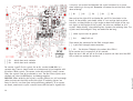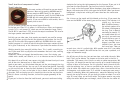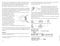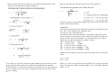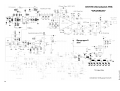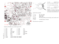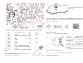
1
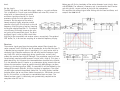
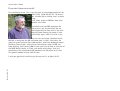
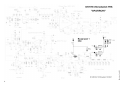
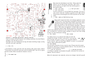
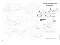
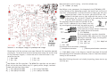
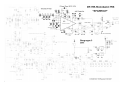
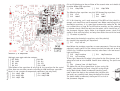
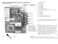
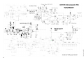
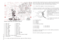
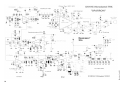
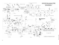
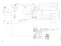
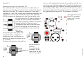
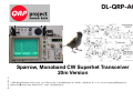
DL-QRP-AG
Revision:1.Oct. 03
Sparrow, Monoband CW Superhet Transceiver
20m Version
© QRPproject Motzener Straße 36-38 12277 Berlin http://www.QRPproject.de Telefon: +49(30) 85 96 13 23 e-mail: [email protected]
Manual by: fiservice Peter Zenker DL2FI email: [email protected]
1
Monoband QRP–CW Transceiver "SPARROW"
Preface:
Technical data:
Description of individual stages:
Local oscillator:
Receiver:
Transmitter:
Transmitter keying and RIT:
Voltage controller:
The first steps
What you need to know
Soldering
Soldering iron:
Before removing components from the pc board
If you don’t know what to do?
Section 1, Voltage regulation, keying section.
Section 2: AF output stage, AF preamplifier stage
Section 3, IF amplifier
Small toroid and component school
Toroid inductors
The formula for powder cores looks like this:
Capacitors
The DDS VFO for the Sparrow
Functions of the DDS:
VFO
Tuning:
Showing the band edges:
RIT (R)eceiver (I)ncremental (Tuning).
XIT (X)mitter (I)ncremental Tuning.
CW-keyer
Changing the keying speed
Memo
AFA
Parts list for the Sparrow DDS VFO
Section 4 VFO-Mixer and counter read out
Section 5: RX input including Lowpass Filter LPF.
2
3
3
3
3
3
4
5
5
5
5
5
6
6
6
7
9
11
13
15
15
17
17
19
19
19
19
19
19
19
19
19
20
20
20
25
27
Section 6 TX Mixer up to the input of T4.
Section 7 Exciter and amplifier up to and including TR1/C86.
Section 8 PA
Wiring diagramm Sparrow
Fitting in the enclosure.
Appendix A Test for section 1
Appendix B Test of section 2
Appendix C Test of section 3
Appendix D Test section 4
Appendix E Test section 5
Appendix F Test section 6
Appendix G Test section 7
Appendix H Test section 8
Appendix I Winding instructions for transformer TR1
Packing list Sparrow
Parts list Sparrow DDS VFO
Parts list Sparrow
Packing list Sparrow
Appendix H, Schematic DDS VFO
29
31
33
43
35
36
36
36
37
38
38
38
39
40
41
42
42
42
43
Schematic Sparrow
44
Block Diagramm
45
Revision:1.oct.03
Index
Monoband QRP–CW Transceiver "SPARROW"
- tentative english translation by Peter Raabye, OZ5DW, 18.04.03
Not verbatim: readability was a priority.
By Peter Solf, DK1HE
Project coordination and editing: Peter Zenker, DL2FI
With support from Jürgen, DL1JGS (Prototypes, manual) and Wolf, DL2WRJ
(Programming of the DDS VFO)
Preface:
Even in times of modern all band technology, there is a continuing interest
in monoband QRP CW transcievers. Most are presented as easily and quickly
built kits, and are thus well suited for both newcomers and oldtimers. The
experience of trouble free QSOs with a home built, simple transciever won’t
compare to using even the most expensive „yen box“: it gives at feeling of
going back to the roots of ham radio.
Revision:1.Oct. 03
Available kits are roughly of two kinds:
1. „Fun transcievers“, designed for QRP use and a minimum of complexity
and component count.
2. Monoband transcievers with a more demanding technique and larger
complexity, but with a comfort of use and performance comparable to more
expensive equipment.
Kits in category 1 usually have direct conversion or single conversion
recievers. Many of these are good constructions, though. They often miss
sensitivity, and as their oscillators often are based on VXCOs, they usually
have a small frequency variation. Due to little RF selectivity, they often
have intermodulation problems from BC transmitters on the 40 meter band.
RF attenuator potentiometers relieves this a little, but at the price of reduced sensitivity. No or bad AGC forces the operator to adjust the AF output
volume. Because of the increasing demands on the construction, most kits
are not offered in version for higher bands than 20 meters.
Kits in category 2 take more time to build, due to a larger component count
and more complex design. Trimming of these kits are also more complicated. Many newcomers won’t build one of these kits, as they want to be QRV
quickly and easily.
These categories of kits have in common, that about 80% come from english speaking countries (why?), and thus offers a problem of high import
and customs costs for europeans. At the wish of the DL-QRP-AG, I developed the monoband transciever described in this document, to respect both
the ease of construction of category 1 and the good technical specifications of category 2.
Peter, DL2FI dubbed it Spatz, in english Sparrow.
Sparrow for small and awake!
Technical data:
- 14,000 MHz to 14,100 MHz CW (or any other Ham band)
- DDS VFO, as stable as crystal control
- High RX sensitivity (typ. 0,3µV)
- High RX input selectivity (good intermodulation characteristics on 40
meters)
- 8 pole Cohn Filter with 400Hz bandwith
- Combined dynamic range of AF and IF of more than 90dB
- QSK
- RIT, XIT
- Frequency read out in morse
- possible addition of an external frequency display (with IF offset)
- possible addition of a relative signal strength read out
- chirp reduction
- PA output adjustable to a max. of 5W
- hardy PA transistor (2SC1969)
- direct monitoring of transmitted signal
- High suppression of spurious signals
- low power consumption (RX=80mA; TX=630mA at 5W Out)
- reduction of external wiring through use of printed circuit connectors.
- easily reproduced toroid inductances
- standard casing (Teko CH2) with printed front panel sticker
Description of individual stages:
Local oscillator:
The VFO is based on superheterodyne principles. This is done by mixing the
stable output of a DDS VFO with the output from a band set crystal oscillator. This will give stable local oscillator operation even in the 6 meter
3
band.
On the circuit:
The DDS VFO gives a 7915-8015 kHz signal, stable as a crystal oscillator.
This is buffered in T2 and input to the Gilbert cell mixer IC4, where it is
mixed with an internal band set crystal
oscillator signal based on Q6. In case of
overtone crystals Dr1 with reduce the 1.
harmonic. On the output of the mixer a
loosely coupled, highly selective parallel
resonant circuit with L5 will clean up the LO
frequency. C38/C39 gives a low loss coupling
to the gate coupled amplifier T1. The output
circuit around L4 further increases the spectral purity of the amplified signal. The local
oscillator signal is sent by C9 or the divider
C35/C36 to the transmitter and reciever mixers, respectively. The optional
JFET buffer, T8, is for low loss coupling of an external frequency display.
Below you will find a simulation of the entire 40 meter input circuit, done
with RFSIM99. The software is Freeware, and is contained on the CD enclosed with the kit, so you are free to play with the components.
IC1 amplifies the received signal after mixing with the local oscillator, and
outputs the 4000 kHz IF.
The antenna signal goes from the transmitter output filter through the
series resonant circuit C75/L9 to the RX preselector. As the PA transistor T7
is blocked during reception (class C operation), Tr2 is only active with its
relatively high inductive reactance, and will only load the antenna signal
very little. D13 with be conducting during transmission, and will thus
protect the receiver from high RF voltages. The preselector consists of two
capacitatively coupled parallel resonant circuits with a high Q. This gives a
good selectivity, and increases the intermodulation characteristics especially in the 40 meter band. D1 works as an attenuator during transmission and
reduces the transmitter signal to prohibit too high AGC voltages, to allow
listening in the keying pauses (QSK). In reception D1 will be blocked by the
voltage of the zener diode D2, and thus increase in impedance. The signal
can be further reduced the optional diode D14. To inhibit further intermodulation effect due to non linear diode characteristics, PIN diodes are used
for D1, D13 and D14, as they work as controllable linear resistors. The
filtered reciever signal is inductively and symmetrically coupled to the
reception mixer IC1 via L2.
4
Revision:1.oct.03
Receiver:
Transmitter:
keying. Key clicks are eliminated.
Voltage controller:
IC6 mixes the local oscillator signal with a 4915 kHz carrier. The 4915 kHz
signal is produced by the internal oscillator of IC6 in conjunction with Q8.
The following capacitatively coupled band pass filter, based on L6/L7,
strips the unwanted mixer products. C58/C59 transforms the high output
impedance of the filter to the input impedance of the amplifier T4. P5
regulates the emitter current, and thus the amplification of the section.
The collector of T4 is loaded by the parallel resonant circuit of L8/C62. A
high Q is achieved through a weak inductive coupling, and thus a high
increase in spectral purity of the transmitter signal. C63 couples the amplified transmitter signal to the following buffer. T5 works as a emitter follower with high input impedance, and thus low loading of L8/C62. The low
impedance output of T5 is directly coupled to the base of T6. R30/R31
places T6 in class B operation (kleiner Ruhestrom ~ 5mA). The dynamic
amplification of the stage is determined by the feedback circiut of R34/
C66/R33. Tr1 transforms the output of T6 to the very low base impedance
of the PA transistor T7 (~5 Ohm) . C68/D12 gives a better dynamic range of
T7 for not quite sinus shaped signals (clamper). R35 places T7 in class C
operation. Tr2 transforms the collector impedance of T7 to the 50 Ohm
level. C71 serves as a compensaton of the inductive reactance of Tr2, which
is not negligeable in higher bands (This increases the efficiency of the
stage). Harmonics are reduced by at least 50 dBc in the three section
output filter of L10/L11/L12.
Revision:1.Oct. 03
Transmitter keying and RIT:
RIT and XIT (fine tuning of the transmitter by fixed RX frequency) is achieved directly in the DDS VFO. The transmitter is keyed softly via T3 as follows: C69 is charged via R24 with a time constant of some 5mSec. On
reaching the gate opening voltage T3 conduct increasingly, giving power to
the transmitter stages. Through this slow increase of the supply voltage,
the maximum transmission power isn’t reached till after some 5 mSec
(rounded flank). After release of the key C69 is discharged via R24 with a
time constant of, once more, some 5mSec. After reaching the gate opening
voltage, T3 will slowly reduce the voltage of the transmitter stages. The
output will reduce to zero within about 5mSec (rounded flank). Through the
easy controlling by T3 it is possible to reach well defined flanks for the
To reduce the effects of varying input voltage, IC8/IC9 is used to regulate
voltages for the individual stages. The kits can work from any supply voltage between 10 and 15 V.
The first steps
What you need to know
You don’t have to be an electronics expert, but you have to know some of
the basics before you delve into this adventure.
The first steps
What you need to know
You don’t have to be an electronics expert, but you have to know some of
the basics before you delve into this adventure.
Colour coding: (Resistors, capacitors, inductances)
You must be familiar with the standard colour coding of electronic components. If you’re not sure, measure with an ohmmeter.
Some 8% of the male populations is red/green colour blink. Many doesn’t
even know. If you are one of these, you should measure all resistors with an
ohmmeter before mounting them.
The color-code chart next page shows how to read the four color bands on
5% resistors. 1% resistors are similar, except that they use five bands
(three significant digits, multiplier, and tolerance). For example, a 1,500
ohm (1.5 k) 5% resistor has color bands BROWN, GREEN, and RED. A 1.5 k,
1% resistor has color bands BROWN, GREEN, BLACK, BROWN. The multiplier
value is 1 rather than 2 in the 1% case because of the third significant
digit.
Because 1% resistors have color bands that are sometimes hard to distinguish clearly, you should always check their resistance using an ohmmeter.
The markings on RF chokes reflect their value in microhenries (µH). Like 5%
resistors, chokes use two significant digits and a multiplier. Example: an RF
5
choke with color bands RED, VIOLET, BLACK would
have a value of 27 µH.
Soldering
into the board as possible. This is not a question of good looks, but an RF
technical must. Resistors should be flush with the pc board, when not
indicated, that they should be mounted standing. Capacitors have to be
Hopefully this is not your first encounter with a
soldering iron. If it is, or this is your first semiconductor project, read the following tips.
Soldering iron:
Only heat the soldering point enough for a good
connection. A small vise for holding the pc board is a great help
The printed circuit board is double sided and all holes are plated-through.
This means that you need not, and indeed should not, solder on the component side of the board.
How to recognize a good and a bad soldering:
GOOD
BAD
Ideal: the soldering point
Too much solder
is rounded and concave.
has been added
Touch pc board and component at the same time with the soldering iron.
Within one or two seconds add solder, to see solder flow at soldering point.
Pull away solder and then pull away soldering iron.
Don’t try to fill up the soldering points with solder. Too much solder leads
to trouble, as it can bride pc board or components. Press components as far
6
flush too. In other words: No components with long wires.
Please read the following, before removing components from the
pc board
Oh Noooo! Sooner or later you have to remove components, that have been
soldered into wrong places, or a parts has to be removed to locate malfunctions.
Get a roll of solder wick. Put the end of the solder wick on the soldering
point to be removed, and push the soldering iron to the wick. After a few
seconds, you pull, as the wick absorbs the solder. Remove the wick (vertically, never to the side!). Repeat this till the soldering point is clean. It
can necessary to reheat the soldering point for the removal of the component. Only heat the soldering point for the necessary time; the copper foil
can lift off from the pc board, if overheated.
If this doesn’t work, you have to cut the component connector and pull it
with a pair of pliers. Contact DL2FI for replacement parts
If you have to remove a transistor, you are strongly advised to cut it on top
of the pc board. The TO-92 soldering points are especially small, and attachments are removed more easily one at a time without damaging the
board.
After removal of the components, the pc board holes are probably filled
with solder. Use a needle. Heat needle and board at the same time, till you
can push the needle through the board. Steel needle don’t take the solder,
Revision:1.oct.03
Use a 50 to 80 W soldering iron if possible. A 0,8
mm pencil tip is ideal. Keep the tip clean. Use a
moist sponge or a moist cotton cloth to clean the
tip regularly during work. On ground areas, you
might need a larger soldering iron tip.
so the hole is freed.
If you don’t know what to do?
Turn confidently to me. This is easy by email to [email protected] by
phone (+49) (0)30 859 61 323. To have an
idea, to whom you ar talking, here’s a photo
of me:
DL2FI, Peter, known as QRPeter. Ham radio
operator since 1964.
I have built and used QRP equipment for
several years, and am convinced, the the
great opportunity for ham radio is the rediscovery of home brewing. My motto is Ham
radio will be again, when it is what is was.
Based on this conviction I founded the DLQRP-AG, a work group for QRP and home brew, in 1997. Since then, the
group has grown to more than 2300 members, who have developed several
excellent pieces of gear, adding to the international succes of QRP and
home brewing. Since january 2002 I have spent a lot of time as chairman of
the DARC Berlin Chapter, as I feel a lot better doing things, than just
complaining. The international QRP movement has taking me on as their
first german member of their Hall of Fame.
Revision:1.Oct. 03
I wish you good luck in building the Sparrow and 73 de Peter, DL2FI.
7
8
Revision:1.oct.03
Now come the electrolytic capacitors. Please note the
polarity. On the body of the capacitor, you’ll find a
minus marking, and you’ll find that the long lead is
the positive pole.
[ ] C85 1µF radial
[ ] C86 1µF radial
[ ] C87 47µF radial
The last capacitor is a 0,22µF MKS Foil capacitor. This type is
used, when a high Q is needed, especially at AF. MKS capacitors
should never be exchanged with X7R capacitors of the same
value.
[ ] C69 0,033 µF MKS Foil Cap 5mm
Many small signal transistors and voltage regulators are made
in TO 92 cases. The component placement drawings show all
components basically from above. When mounting, please
note the direction of the rounded part of the casing.
Please do not mix up the two voltage controllers, which are
both in TO92 (the 8 V regulator is marked LO8, and the 6 V
regulator marked LO6). Voltage regulators like these look
simple, but are quite complex inside. They contain several dozen components, and delivers a constant output voltage, as long as the input voltage is
at least 1 V over the output voltage.
[ ] IC8 78LO6
[ ]IC9 78LO8
Here follows a small capacitor with the marking 104, which means 100 nF
Capacitors of type X7R are mainly used for blocking RF. Their Q isn’t good,
which makes them unusable for resonant circuits.
The diodes have a ring around their body to mark the
cathode. For diodes in plastic casing this is easy to see,
but on diodes with glass casing, it can be quite difficult.
In this section, you’ll use one large 1N5402 in plastic as a protection
against wrong connection of power.
[ ] D10 1N5402
The two pole connectors have a security nose. Please note the correct
position on mounting, to avoid problems later on. The side with the nose is
marked in the placement diagram.
[ ] 2 pole 12V connector
[ ] 2 pole Key connector
[ ] Bridge as marked on placement diagram, and place 2k2 resistor on
bottom side of pc board.
[ ] C93 100nF 104
When all components are mounted, please run through check of appendix A
Section 1, Voltage regulation, keying section.
The first section to build contains the voltage stabilizers for the different
voltages, and the keying circuit.
You begin with the components having the lowest building height, mainly
resistors and small capacitors.
Revision:1.Oct. 03
[ ] R24 27k
9
10
Revision:1.oct.03
Now the diode in plastic casing, - mind the cathode ring!
[ ] D5 1N4004 (or equal)
Section 2: AF output stage, AF preamplifier stage
Revision:1.Oct. 03
Please begin with the resistors once more. R10 and R12 should be mounted
standing up. To do that one lead must be bent back along the resistor body.
In the placement diagram, a circle marks which side the resistor is supposed to stand on.
[ ] R10 560R
[ ] R11 18k
[ ] R12 18k
[ ] R14 22k
Now follows a new component, the integrated circuit TDA7050 in DIP
casing. Because of the production process, the lead of such an IC are always bent a little outwards. To fit the IC to the pc board, you will have to
prebend the leads a little. To do that, you roll the IC on a flat
surface till the leads are at a right angle with the casing, as shown
in the picture. Pin 1 of the IC is found by the markings on the top
of the IC. You’ll find either a notch or a dot.
The placement diagram shows the position of the
notch. The IC is mounted in the pc board, and initially two diagonally placed leads are solder to position the IC. Check if the IC
is flat onto the pc board. Correct if necessary.
Then solder the rest of the leads.
[ ] IC3 TDA7050
The three electrolytic capacitors should be
placed carefully. Now, what was this thing about
electrolytic capacitors? Right, the long lead is
the positive terminal.
[ ] C31 10µF rad
[ ] C33 100µF rad
[ ] C34 47µF rad
[ ] R41 10R
Last mount the to connectors. (Marking!)
[ ] Headphone connector
[ ] Volume potentiometer connector
[ ] C105 100nF, shown in the diagram, shouldn’t be placed till the definitive mounting of the headphone connector, where it should be soldered
directly to the connector.
Now after finishing the work, and visually inspecting, please turn to appendix B for test.
Now follows the film capacitors. The WIMA film capacitors are non-polarized, and can be placed either way. It is good practice, though, to mount
them with their text side visible.
[ ] C28 0,01µF film RM5
[ ] C29 0,22µF film RM5
[ ] C30 0,01µF film RM5
[ ] C32 0,047µF film RM5
11
12
Revision:1.oct.03
C18 and C19 belongs to the oscillator of the second mixer and should also
be either NP0 or COG capacitors.
[ ] C18 150pF NP0
[ ] C19 150pF NP0
The following four capacitors are plain X7R decoupling capacitors.
[ ] C16 22nF
[ ] C20 22nF
[ ] C25 100nF
[ ] C22 100nF
C17 is for trimming, and is only necessary if the BFO can’t be pulled far
enough, and should thus not be mounted now. Before continuing with the
electrolytic capacitors, it is a good time to mount the socket for IC2. We
use a socket here, as large ICs are difficult to unsolder, and the socket gives
us a better chance. Mind the notch on the socket, which should face as in
the placement diagram. Again: Solder in to diagonal corners, check if the
socket is flush with the board, and only then solder the rest of the leads.
[ ] IC socket 16 pole flat
Now mount the electrolytic capacitors, mind the polarity!
C21 shouldn’t be mounted yet! Important!
[ ] C27 33µF 16V rad
Revision:1.Oct. 03
Section 3, IF amplifier
We begin once again with the resistors
[ ] R3 220R
[ ] R4 18k
[ ] R5 120R
[ ] R6 2k2
[ ] R7 56k
[ ] R8 27R
[ ] R9 1k5
[ ] R13 470R
Then follows a few capacitors of very high Q, the capacitors for the crystal
filter. Here we use either ceramic capacitors or NP0 multilayer capacitors.
Here it is not a matter of temperature coefficient, but only the Q.
[ ] C11 220pF NP0
[ ] C12 220pF NP0
[ ] C13 220pF NP0
[ ] C14 220pF NP0
[ ] C15 220pF NP0
Now follows the tantalum capacitors as new components. These are also
polarized, usually you’ll find the value printed on the body and at one lead
a PLUS sign. Tantalum capacitors are used, when focus is on low losses by
high capacitance.
[ ] C26 10µF tantalum
[ ] C23 10µF tantalum
[ ] C24 1µF tantalum
To the right, above the IC socket is the place for the film trimmer, that is
going to be used to trim the BFO. Careful when soldering: The plastic melts
easily.
[ ] C94 trimmer 7mm 2,5-50pF black
The diodes D3 and D4 are germanium in glass casing. Be
careful, when bending the leads, the glass casings break
easily! Both diodes should be mounted standing, you’ll
need to bend the lead on the cathode side (the one with
the band) very carefully back along the body of the diode.
The diode should be mounted, where you find a circle in
the placement diagram.
13
is to put a cut resistor lead between the crystal and board as a spacer,
when soldering in the crystal. Remember to remove the resistor lead, when
done soldering!
[ ] Q1
[ ] Q2
[ ] Q3
[ ] Q4
[ ] Q5
Over and to the right of Q1 and below Q4, you’ll find two holes in the
board. In these holes, you should solder in 2 cut resistor leads or other
wire bits, and bend them at a right angle at about half height of the crystals. Again at half height of the crystals, the wires are soldered to all 4
crystals. Solder briefly, a hot soldering iron shortens the soldering time. The
crystals could be damaged if they are cooked for too long.
[ ] solder crystal cases to ground
[ ] C21
100µF 16V rad
Then mount the connector for the field strength meter.
[ ] 2 pole field strength meter connector
[ ] IC2 Put A244 or TCA440 in the socket. Mind PIN 1!
Go to section test in appendix C of this manual.
When the test is OK, we will at first look at toroids and then build the DDS
VFO, as both are needen for section 4.
AA143 bent end= cathode
AA143 bent end= cathode
For section 3 you’ll find 4 crystals, Q1 to Q4, marked 4,000 MHz in a
separate bag. These 4 should under no circumstances be put together with
the other 4 MHz crystals. The reason: to be able to build a steep, narrow
filter, the crystals have to be selected as sets. The four filter crystals were
checked and paired at QRPProject, and belong together.
WARNING: When soldering the crystals, capillary effects can pull up enough
solder to short out the leads under the crystal. If underlay spacers are
found in the kit, use them (but we have delivery problems). If no spacers
are found, mount each crystal a small distance off the board. A good trick
14
Revision:1.oct.03
[ ] D3
[ ] D4
Small toroid and component school
Toroid inductors
In the next section we’ll need to use som toroid
inductors. We use high quality AMIDON toroids,
like our american QRP friends. In the general
appendix of the manual, you’ll find the FAQ of the
DL-QRP-AG with some general information on
toroids. If you are unfamiliar with toroids, that is
a good place to start.
In the 40 meter Sparrow we use several types of toroids:
In the low pass filter T37-6, yellow, in the band pass filters and resonant
circuits T37-2, red (except L3, where we use the somewhat larger T50-2).
The PA RFC is wound on a FT37-43 and the output transformer TR2 also on
the larger powder core toroid T50-2.
Initially you can take note, that powder core toroids are used for narrow
band applications and the ferrites for wide band applications. On the CD,
you will find the Mini RK program by Wilfried, DL5SWB. With this small,
helpful program it is piece of cake to calculate the proper number of turns
for a given inductance, or the inductance if you know the number of turns.
Revision:1.Oct. 03
Winding toroids gives many kit builders fears. This is unfair, according to
me. If you meet with no prejudice and remembers the basic rules, nothing
can go wrong.
Important: a wire put through the toroid means a turn. For training, you
should wind a toroid, we’ll take L4, as is is an inductor we need in section 4.
Cut about 25 cm of the 0,3 mm copper wire, take the toroid and put in one
end of the wire. Now one turn is done, but STOP!
Look at your work, and think about how you put the wire through the ring.
There are two possibilities. You can put in the wiere from behind, forwardly,
as girls used to sew, or from the front backward. For the RF is equal, but for
the mounting, it is not, as the holes in the pc board are made for a specific
direction. Each and every one of us should put the wire the way he wants.
But this forces a winding direction, to have the proper geometry of the
toroid.
If you put in the wire from the back forward, you must continue winding
clockwise for having the right geometry for the Sparrow. If you put in the
wire from the front backward, you have to wind anti clockwise.
This is only so for the Sparrow. Other developers have other preferences.
Wayne, the constructor of K2 wind opposite to DK1HE. When you know the
background a simple test winding will soon show how the constructor
planned it.
Put 23 turns on the toroid well distributed on the ring. If you count the
turns on the INSIDE of the toroid, you can’t be wrong. The inductor in the
picture, e.g., has 8 turns.
Well distributed means, that
the wished number of turns
fills about 270 degrees of
the ring. That is about the
maximum for toroids. If you
are careful about this when
you wind, you won’t need
to pull the turns apart later
on, even though it to some
degree is possible. turns
shouldn’t cross, but should
be in one layer. Take care
on each turn, that it is pulled tight. With powder cores this is no problem,
as the edges are smooth. But with ferrites this can pose a problem, as the
edges are somewhat rough.
Cut off the rest of the wire, but not too close, and solder the ends. Whats
best? That’s up for debate. The lacquer on the wire used in the kits is
solderable. That means, that it burns or melts at solder temperature. With
thin wires, till about 0,8 mm the heat capacity of a standard soldering iron
suffices to burn of the lacquer. For this purpose I touch the end of the wire
with the soldering iron, as close as possible to the toroid core, and put on
a lot of solder. You should see a proper drop. after a short while the lacquer
disintegrates, and smoke erupts. It is advised to move your nose away, the
smoke is unhealthy. When the smoke erupts, move the soldering iron slowly
towards the end of the wire, till you have put solder on about 1 cm of the
wire. If it won’t flow, put on fresh solder. The lacquer remains are pushed
off by the solder. When you are through, check if the wire has solder all the
15
You will often need a transformer. These can be symmetrical or unsymmetrical. Symmetrical means without ground in this context. No end of the coil
goes to ground or decoupling capacitor. Such symmetrical coils are built so
that their turns lie centered over the main coil.
As an example take L5 from section 4. The main coils needs 23 turns, the
secondary 8. To place the secondary symmetrically, we need to
count INSIDE the ring. 23 divided
by 2 is 11,5, the center thus is at
11,5 turns. The 8 turns of the
secondary should be made as 4
plus 4 before and after the 11,5th
turn. The half turn is impossible,
as each turn put through the ring
is an entire turn. We must accept
a slight assymmetry, and must
decide for 11 or 12 as center. 11
minus 4 equals 7, so the secondary should be started on turn 7.
In the picture is shown a coil of 14 turns, with a secondary of 4 turns. Half
of 14 is 7, minus one half of4, gives the start of the secondary at turn 5 of
the main coil. That is, you see 5 turns of the main coil before and after the
secondary.
WARNING:
In the kit, the numbering of coils are not the same: L2 and L3 have the
resonant coil numbered 1 and 2.
This sounds a lot more complicated than it is. When you have done it once,
it becomes quite easy.
16
That much about practical things. In the next section, I will tell those of
you, who want to understand your Sparrow, about the
calculation of the coils.
The band filters and resonant circuits in the
Sparrow are all parallel resonant circuits, as
shown to the left of the example from the front
end. As toroids are not variable, we must work
with variable capacitors. The total capacity will
be calculated as shown. We will when working
with our pocket calculator, assume that the capacitors are in the center
position. On the CD you will find an Excel spreadsheet, which also calculates on start and end values. For calculation of the inductance, we first need
the total capacity of the circuit.
We begin by the capacitor coupling. C1 and C2 are in parallel, so capacities
add up. C1/2=C1 + C2.
C1/2 and C3 are in series. For series coupled capacitors the formula tells
We solve further by multiplying on both sides with C3:
Then multiply by (C1 + C2)
And the multiplication with Cges:
Then only the division by (C3 + C2 + C1) is left, and Cges is:
Revision:1.oct.03
way around. This is really important, as most failures of home brew transcievers come from badly soldered inductors wound with lacquered copper
wire. With thicker wire, you need to scrape off the lacquer with a knife.
Very carefully, so that the wire isn’t nicked and will break.
Do exactly the same to the other wire end, and your inductor is ready.
When the total capacity is known, we use Thomsons formula to find the
necessary inductance for the given frequency:
Now we only have the calculation of turns for the toroid left.
The formula for powder cores looks like this:
On the CD, you’ll find the small programm Mini RK, with which such calculations can be done directly.
Capacitors
The years have brought several different standards for marking of capacitors. This is the cause of much confusion, but
I will try to shed a little light on it.
One method, much used for industrial and multilayer types (the small
cushion shaped, mainly brown or blue, capacitors), gives the value and the
power of ten of the value, based on 1 pF. The code consist of 3 digits,
where the last digit represents the number of zeros:
100 = 10 and 0 zeros = 10pF
101 = 10 and 1 zero = 10 0pF
102 = 10 and 2 zeros = 10 00pF = 1nF
103 = 10 and 3 zeros = 10 000pF = 10nF
104 = 10 and 4 zeros = 10 0000pF = 100nF
Another standard uses the decimal name of the power of ten as decimal
point:
Revision:1.Oct. 03
1p5 = 1,5 pF
2n2 = 2,2 nF
As shown, we now only need the wished frequency and the freshly calculated value for total capacity to calculate the inductance for resonance.
The values for L, f and C are in Henry, Hz and Farad, that is quite unhandy.
If f is in MHz and C in pF, we can directly calculate the size of the inductance in Henry.
Often a J is used in stead of the p for picofarad. The J marks a capacitor
with a 5% tolerance. 100J represents 100pF+/- 5% and 150J represents
150pF +/- 5%
17
The list of signs for tolerance are:
B ±0,1pF
C ±0,25pF
D ±0,5pF
F ±1pF(if > 10pF dann ±1%)
G ±2pF (if > 10pF dann ±2%)
H ±1,5pF
tors, when some component RF wise should be grounded, but not DC wise.
Values between 1nF and 100nF are the most common.
J ±5%
K ±10%
M ±20%
S -20...+50%
Y 0...+100%
Z -20..+80%
Those who order capacitors them selves or salvages them from old gear,
have to be very careful which capacitor is used for what purpose. In kits
you don’t have to worry that much, the developer and QRPProject has made
the choice.
Some of these are so uncommon, that I havent seen them. 5% is really the
most common. This marking is mainly used for discoid capacitors.
Film capacitors usually use the µFarad as base
0,22µF = 200nF
0,033µF = 33nF
0,0015µF = 1,5 nF
Ceramic capacitors usually have an additional color coding, representing
the temperature coefficient. To us the most important are the ones with a
black, yellow or violet stripe. Black means NP0, yellow means NP220 and
violet means NP750. A lot of others exists, but are uncommon.
It is very important to choose the right capacitor for the job. The material
of which the capacitor is made, makes a large difference. The reason is
mainly the different Qs of materials.
Multilayer capacitors come as NP0 types, even those with a high Q. Their
(### fordel ###) for us kits builders is, that they are lacquered and thus the
print on them not so easy to damage, as it is in ceramic capacitors.
Multilayer capacitors are mainly cushion shaped. (### desværre ###) it isn’t
possible to distinguish them from simple X7R or ZU5 capacitors just by
looking.
X7R and ZU5 are materials of lesser Q. They are good as decoupling capaci18
Revision:1.oct.03
Ceramic capacitors mainly have a high Q. They are preferred i RF circuits,
e.g. as parallel capacitor in resonant circuits. Ceramic capacitors mainly
come as disks or small squares.
The DDS VFO for the Sparrow
than 10 Hz. In the Sparrow only the RIT LED is used.
In the next section we will build the DDS VFO. Those who ordered it ready
made, will probably want to read the description and user manual anyhow,
to be able to use the VFO afterwards.
RIT
(R)eceiver (I)ncremental (Tuning).
Our QRP friend Steven Weber, KD1JV, from the White Mountains of New
Hampshire is a proponent of a philosophy much like the DL-QRP-AG: When
you can find an equally good, cheap, solution, you prefer that one. He has
created a DDS stage, which can be used for any VFO in the interval 100 kHz
to 9,5 MHz. He doesn’t use any expensive components, and no expensive
high frequency oscillator. On my wish he has given over the project to DLQRP-AG, for our members to have access to a cheap DDS VFO in kit form.
The firmware has been modified a little for the Sparrow.
Functions of the DDS:
The RIT is activated by the RIT switch, and the RIT LED shows if it is on. On
using the tuning knob, only the recieving frequency changes. The tuning
rate corresponds to the one chosen before activating the RIT, but can be
changed by pushing the RATE knob. On switching off the RIT, the previous
tuning rate of the VFO is restored.
XIT
(X)mitter (I)ncremental Tuning.
VFO
When activating the XIT, the reception frequency remains unaltered, but the
transmitting frequency is changed. Activate XIT by pushing the Memo
switch, when the RIT is activate.
7,915 MHz to 8,015 MHz DDS gives the local oscillator coverage from
18,915 MHz to 19,015 MHz. Mixed with the IF of 4,915MHZ, that will give
an RX/TX frequency of 14,00 to 14,100 MHZ. Starting frequency is programmed at 14,060 MHz.
CW-keyer
The VFO has an integrated electronic keyer for speeds between 10 WPM (50
cpm) and 40 WPM (200 cpm).
Revision:1.Oct. 03
Tuning:
The frequency of the VFO changes on turning the knob, according to the
preset tuning rate. The frequency gets higher, turning clockwise.
Choice of tuning rate
A short push on the VFO tuning knob shifts tuning rate. There are 4 Tuning
rates: Step1= 10Hz, Step2 = 30Hz, Step 3= 100Hz Step 4= 1000Hz. The
chosen rates are acknowledged by blinking of the RIT-LED: Step4= 4times
blinking, Step 3 = 3 times blinking aso. At power on the Sparrow DDS start
with Tuning Rate 3 =100 Hz/step followed sequential by 30 Hz, 10 Hz, 1
kHz and then 100 Hz again every time you touch the shaft.
Showing the band edges:
HAND key:
If the DIT contact is closed during power on, the internal keyer electronic is
switched off and the DIT contact can be used for a pump key or an external
keyer.
Changing the keying speed
The keying speed is changed by pushing the Rate switch, and the paddles.
The Rate switch has a 0,5 s delay before changing the rate. If a paddle is
activated within this period, it will change the keying rate. The VFO stays in
this mode till the Rate switch is released.
The dot paddle raises the speed, the dash paddle lowers it.
When the VFO is at its lower or upper edge, the LED blinks. Otherwise it
wouldn’t have been possible to tune to the band edges with any other rate
19
While changing keyer speed, the transmitter keying is disabled, and the side
tone oscillator will sound an A to give the user a feel for the actual keying
rate. Holding down the paddle will repeat the change till the upper or lower
limit is reached. This rate change is in steps of 2 WPM (10 cpm).
Memo
There is one memory position.
One long push (> 1 s) stores the present frequency in memory. The RIT LED
blinks twice to confirm, if the RIT is off.
A short push switches between present frequency and stored frequency. The
yellow LED blinks once, when the frequency changes. It starts on 14060 at
power on. When no memory frequency is stored, the VFO will go to 14,060
MHz in stead.
AFA
22 uF /10VSUB-MINATURE 4x7 mm
Diode 1N4148
LED red
3,3 V Voltage regulator
100 R 5% 1/4W
10 k
5% 1/4W CARBON FILM
220 R
5% 1/4W
2N7000
TO-92 MOSFET
CLOCK 25.000 MHz CMOS 1/2 SIZE DIP
CPU
ATMEL A90S2313-PC10, programmed
DDS ANALOG DEVICES AD9835BRS
Shaft encoder
Crystal 4096 kHz
Transistor 2N3904
PC Board
1
1
1
1
1
1
2
1
1
1
1
1
1
1
1
(A)udio (F)requency (A)nnounciation
A longer push on the tuning knop reads the frequency out in morse via the
side tone. The values for 100kHz, 10kHz and 1kHz are read out, the
accuracy is abt +- 1kHz. In RIT and XIT mode the AFA gives out the
difference between TX and RX frequency with a higher resolution.
0.1 uF
0.01 uF
100 pF
22 pF
220 pF
33 pF
100 uH
2.2 uH
10 k
22 k
270 R
3k9
470 RSMD
68 R
2N3904
0.1 uF
20
SMD 0805
SMD 0805
SMD 0805
SMD 0805
SMD 0805
SMD 0805
SMD 1008
SMD 1008
SMD 0805
SMD 0805
SMD 0805
SMD 0805
0805
SMD 0805
SOT-23 SMD
CERAMIC MONO
2
11
2
2
1
3
1
2
1
1
1
1
1
2
1
1
Revision:1.oct.03
Parts list for the Sparrow DDS VFO
Revision:1.Oct. 03
[ ] AD9835
[ ] C2 100nF
[ ] R4 270R
[ ] C4 100p
[ ] C3 10nF
[ ] C7 33pF
[ ] L1 2,2µF
[ ] R3 3,9k
[ ] C5 220pF
[ ] C9 10nF
[ ] C1 100nF
[ ] L2 2,2µF
[ ] C8 33p
[ ] C6 100p
[ ] C10 10nF
[ ] C13 10nF
[ ] R5 10k
[ ] Q2 2N3904
[ ] R8 470R
[ ] R6 68R
[ ] C15 33pF
[ ] R7 22k
[ ] C14 10n
[ ] L3 100µF
[ ] C21 10nF
[ ] R9 68R
[ ] C16 10nF
[ ] C23 10nF
[ ] C22 10nF
[ ] C17 10nF
[ ] C11 22pF
[ ] C12 22pF
[ ] C18 10nF
BEWARE, modification:
470pF from PIN 1of the processor to ground, and 10 kOhm from
PIN 1 to PIN 20 (not 4p7 as shown in the photo)
21
[ ] 25 MHz Oscillator
[ ] IC Socket
[ ] R2 10k
[ ] Q3 2N7000
[ ] Q1 2N3904
[ ] R12 100R
[ ] D7 1N4148
[ ] X1 Crystal 4,096 MHz
[ ] U1 3,3 V Voltage regulator, take care on mounting, oblique!
[ ] C19 22µF
[ ] R10 220R
[ ] C20 100nF
[ ] R1 220R
[ ] connection wire for RIT LED
[ ] connection wire for Rate switch
TEST
To test the VFO roughly, the connector at J1 has to be
connected. Look at the wiring diagram to connect the
shaft encoder correctly. If you connect a piece of wire
(about 10 cm) to the point marked RF on the bottom
side of the pc board, you should be able to hear the
DDS VFO on a receiver. The initial frequency is 7,975
MHz, with the shaft encoder, the VFO should tune from
7,910 MHz to 8,020 MHz. (Resulting in an end
frequency of 13,995 MHz to 14,105 MHz after mixing
with Xtal Oscillator and IF later on.
U1 Pin
22
LayOut
Prepare J1.
In the kit you will find the connector and several crimp contacts. As
nobody has the special crimp tool for the little contacts, we will solder the
Revision:1.oct.03
The DDS VFO should be mounted with the 20 mm stand
offs and the long M3 screws to the lower right position:
wires on to the contacts. For that purpose the wire should be put in the
upper part of the contacts, and the upper part of the contact should be
pushed together witd a pair of pliers. Then the wire and contact is soldered
with a LITTLE solder. The contact is pushed into the connector till the little
notch locks, so that the contact won’t pull easily out of the connector.
Test the VFO as described in the appendix.
Revision:1.Oct. 03
When everything works, we will build the heterodyne mixer that shall give
the local oscillator frequency in conjunction with the DDS.
23
24
Revision:1.oct.03
care must be taken, that the wire ends are, where they should be to fit the
holes in the pc board. The right winding direction is important. If the wire
is put in from the back forward, the winding should be clockwise.
[ ] L4 Toroid T37-6 (yellow) 17 turns 0,3mm copper wire
L5 becoms a secondary. As seen in the diagram, this should be symmetrically wound on the primary. It is important, that the turns are wound in the
same direction as the primary. The
drawing makes this clear.
BEWARE: the number of turns in the
drawing does NOT correspond to the
actual numbers.
3/4 is the primary, 1/2 is the secondary.
[ ] L5 Toroid T37-6 (yellow) 20/7
0,3mm copper wire
Revision:1.Oct. 03
Section 4 VFO-Mixer and counter read out
[
[
[
[
[
[
[
[
[
[
[
[
[
[
]
]
]
]
]
]
]
]
]
]
]
]
]
]
R19 47K
[ ] R18
R16 2k2
[ ] R17
Dr.1 left out
[ ] R15
R37 100K
[ ] R38
C50 100pF
[ ] C89
C45 10nF
[ ] C46
C44 47nF
[ ] C42
C41 120pF
[ ] C43
C39 330pF
[ ] C38
C36 47pF
[ ] C35
C37 22nF
[ ] C90
C91 10nF
[ ] C96
C98 ceramic trimmer 10-30pF
C40 left out
[ ] DR1
47K
2,2K
1k
1K
22nF
22nF
82pF
82p
47pF
330pF NPO
10pF
ceramic trimmer 10-30pF
[
[
[
[
[
]
]
]
]
]
IC4 NE612/SA612
T1 BF244A
T2 BF199
T8 BF244A
Q6 11MHz/32pF HC18U
[ ] C47 left out
[ ] C49 left out
[ ] C51 left out
[ ] C48 left out
[ ] C40 left out
If a counter is to be connected, you can use the soldering connection at
point Counter on the PCB
Finish this section by doing the tests of appendix D
left out
L 4 is a simple, one layered coil with 0,3mm copper wire. When winding it,
25
26
Revision:1.oct.03
[
[
[
[
[
[
[
[
]
]
]
]
]
]
]
]
C7
C9
C70
C77
C79
C81
C83
C75
56pF
[ ]
150pF NPO
[ ]
22nF
[ ]
120pF COG [ ] C78
56pF COG [ ] C80
56pF COG [ ] C82
56pF COG [ ] C104
film trimmer green
C8
22nF
C10 150pF NPO
C76 56pF
330pF COG
330pF COG
120pF COG
22nF optional
[ ] C97 ceramic trimmer 5mm 10-30pF
[ ] C99 ceramic trimmer 5mm 10-30pF
[ ] C100 ceramic trimmer 5mm 10-30pF
[ ] L1
toroid T37-2 red 21 turns 0,3mm copper wire
[ ] L2 toroid T37-2 red 20/5 turns 0,3mm
copper wire BEWARE 3/4 = secondary
L3 should be wound on a T50-2 ring, the only
larger red ring.
[ ] L3 toroid T50-2 red 35/10 turns 0,3mm
copper wire BEWARE 3/4= secondary
[
[
[
[
RFC 10uH SMCC
toroid T37-6 yellow 16 turns 0,5mm copper wire
toroid T37-6 yellow 17 turns 0,5mm copper wire
toroid T37-6 yellow 16 turns 0,5mm copper wire
Section 5: RX input including Lowpass Filter LPF.
[ ] R1
[ ] R2
470R
1k
[ ] R36
[ ] R40
1K
Trimming value (optional)
Revision:1.Oct. 03
Please be careful with the orientation of the IC. Pin 1 is in the notch end
of the IC
[ ] IC1 NE612/SA612
The following diodes must be identified under magnifying glass, as they
look very much the same. On the glass casing you will find small, but
legible, print.
[ ] D1
PIN-Diode BA479
[ ] D2
ZPD 4V7
[ ] D13 PIN-Diode BA479
[ ] D14 PIN-Diode BA479 (optionals)
Then follows the capacitors
[ ] C1
22nF
[ ] C2
[ ] C3
560pF NPO
[ ] C4
[ ] C5
2,2pF
[ ] C6
]
]
]
]
L9
L10
L11
L12
When you have mounted all components, go to the test in appendix E
56pF
22nF
2,2pF
27
28
Revision:1.oct.03
[ ] L6
toroid T37-2 red
20/7 turns copper wire 0,3mm
1/2 are the coupling winding.
[ ] L7
toroid T37-2 red
20 turns copper wire 0,3mm
BEWARE: L7 should be wound opposite to the rest of the coils because
the location of the PCB holes is
geometrically oppotite.
[ ] Dr.2
[ ] IC6
[ ] T3
[ ] D11
1N4148)
[ ] Q8
RFC 47µH SMCC
NE612/SA612
BS250 TO92
ZPD 5V6 (Carefully check marking, don’t confuse with
4,915 MHz Crystal HC18U
Go to the test in appendix F
Revision:1.Oct. 03
Section 6 TX Mixer up to the input of T4.
[
[
[
[
[
[
[
[
[
[
]
]
]
]
]
]
]
]
]
]
R25
R27
C52
C54
C56
C58
C64
C88
C101
C102
330R
18K
47nF
220pF NPO
56pF NPO
68pF
47nF
3,9pF
ceramic trimmer
ceramic trimmer
[
[
[
[
[
[
[
]
]
]
]
]
]
]
R26
R28
C53
C55
C57
C59
C65
22K
3,3K
22nF
220pF NPO
3,9pF
470pF NPO
47nF
5mm 10-30pF
5mm 10-30pF
29
30
Revision:1.oct.03
Ferrite bead placed over collector of T5
The driver 2N2219 is in a TO39 metal casing. BEWARE, the casing is connected to the collector, and is on positive potential. Here it is easy to short
out, while measuring!
Revision:1.Oct. 03
Section 7 Exciter and amplifier up to and including TR1/C86.
[ ] R29
[ ] R31
[ ] R33
[ ] R34
[ ] C60
[ ] C62
[ ] C63
[ ] C66
[ ] C74
[ ] C92
[ ] C103
[ ] T4
[ ] T5
lead
2k2 Trimming value
[ ] R30
8,2K
[ ] R32
10R left out if too much output
10R
47nF
[ ] C61
100pF
12pF
47nF
[ ] C67
100nF
47µF careful about polarity
ceramic trimmer 5mm 10-30pF
BF199
BF199 + Ferrit bead on collector
Diagram left of BF199, note that it is not the
standard EBC configuration
33K
150R
View of the bottom
[ ] T6
2N2219A with underlay
[ ] L8
toroid T37-2 red
20/5 turns 0,3mm copper wire
reduce secondary windings if too
much output
[ ] Dr.3
RFC 47µH SMCC
[ ] Tr.1
Two hole core
primary 5 turns 0,2 mm copper
wire, secondary 1turn 0,5mm copper wire
A thorough description of how to
47nF
47nF
wind TR1 is found in appendix I
[ ] P5
trimmer potentiometer 10k PT6LV
Go to test in appendix G
31
32
Revision:1.oct.03
[ ] 2SC1969
[ ] Tr.2
FT50-43 primary 4 turns isol.
mounting wire, secondary 7 turns 0,5mm copper
wire on the larger black toroid.
Begin with the secondary. Begin from the back
forwards, winding counterclockwise, 7 times
through the ring. Then the primary: the mounting wire from behind
forwards through the
ring.
Section 8 PA
[ ] R35
47R
[ ] C71
left out
[ ] C73
1µF 63V MKS2 RM5
[ ] Dr.4
RFC 47µH on FT37-43
the smaller black toroid
[
[
[
=
] D12
1N4148
] C72
100nF
] C68
22nF
11 turns 0,5mm copper wire on
BEWARE DR4 should be wound counterclockwise to fit the holes.
Revision:1.Oct. 03
and then CLOCKWISE 4 times through the ring.
The power transistor 2SC1969 is more than enough for the QRP Sparrow,
which makes it close to indestructible in this setup. Here you will also have
to take care in measurements as the collector is connected to the casing.
Because of this it has to be mounted on an isolator. It is mounted on the
pc board, so that it is flush with the back edge. The back wall of the enclosure will work as a heat sink. Between the transistor and the enclosure, a
grey silicone washer will fit over the screw.
Now test according to appendix H
33
34
Revision:1.oct.03
Fitting in the enclosure.
In the kit you will find a printed fil for the front and back and also a covering film for the front and back to avoid pull out, and the drilling guides.
Begin with the four holes for the pc board. The pc board should touche the
back wall, of the enclosure to make it possible to fix the PA transistor screw
pull out.
Drill the front and back according to the drilling guide, test all components
in their respective holes, to find any errors.
Fix the pc board in the enclosure with the 8 mm standoffs and the short M3
screws. Fix the potentiometers, connectors and switches according to the
diagram below. Don’t forget the external components shown ind the diagram. Cut the wires to the 2 and 3 pole connectors neither are too long or
too short to fit.
The fuse socket will be best fitted above the PA transistor on the back wall.
Put in the DDS VFO with the 20 mm stand offs and the long M3 screws in
the position front right.
Connect all connectors and power, and repeat the tuning of all trimmers.
Set the output properly with the potentiometer P5.
Revision:1.Oct. 03
Parts list for mounting in enclosure
[ ] 1 Sparrow enclosure
[ ] 1 Potentiometer 2k2log (Volume)
[ ] 1 Stereo connector, headphone
[ ] 1 Stereo connector, keyer
[ ] 1 2,1mm coaxial power connector
[ ] 1 Switch SPST RIT
[ ] 1 Power switch SPST
[ ] 1 Fuse socket
[ ] 1 Fuse 1A
[ ] 4 Stand offs 8 mm
[ ] 1 stand off 20mm
[ ] 4 Screws M3x5
[ ] 1 screws M3x25
[ ] 1 1kOhm
[ ] 2 100nF
Below the enclosure, you will fit 3 rubber feet. To front, one back. 4 feet
makes the Sparrow wobbly.
to the enclosure.
Allways put a piece of wood under the enclosure when drilling, to avoid
35
1. Visual inspection
As the first test, all section should first be inspected with a magnifying
glass for shorts. Take this test seriously! Even expert solderers see a bent
lead or a splash of solder creating a short. And missed soldering points
isn’t less unpleasant. More often than you would think a component is
neglected and not soldered in. Check also for the correct parts in the correct places. Are electrolytic capacitors polarized correctly? Diodes?
2. Resistance test
Measure with and ohmmeter the resistance between plus and minus on the
pc board. It is OK as long as there isn’t a short.
3. Smoke Screen test
If the Sparrow passed the resistance test, you can apply power. It is wise to
use a regulated supply with a current limiter.
Before connection the power supply, the current limiter should be set for a
minimum. At this point it is stressed, that the power supply always should
be turned on first, the apparatus under test, afterwards. This is general, not
only for kit testing. The reason: When turned on, many power supplies
present a brief voltage peak, which can be large enough to damage the
apparatus under test. When the Sparrow is connected to the power supply,
you will keep one eye on the power supply and one on the pc board. If
smoke rises, you’ve got a pretty good indicator of malfunction. The same is
true for currents above 10 mA. The protection diode D10 is coupled, so that
wrong polarity results in a short.
4. Measuring voltages
MP 1 Should be + 8V against ground
MP 2 Should be + 6V against ground
MP 3 Should be + 8V against ground, 0 V when the key connector is grounded.
Is a voltage is missing, repeat the visual inspection. When all is OK, continue with section 2.
Appendix B
Test of section 2
1.
36
visual inspection
2.
Resistance test
3.
Smoke Screen test
4.
Functional test.
Connect a pair of head phones to the connector marked Earphone. Best
with the wires of the 2 pole pc board connector soldered to the earphone
socket. Don’t shorten the lead for now, save that for fitting in the enclosure. Solder the volume potentiometer on to the 3 pole pc board connector as
shown in the diagram.
The Test:
When you touch the middle connector of the volume potentiometer, you
should hear a loud humming, maybe even some broadcast radio. The latter
is dependent on how near you are to the closest broadcast transmitter and
how many antenna wires you have in your shack. The more RF in the room,
the more broadcast you hear.
The same goes for MP 4, remember though, that the volume is dependent
on the volume potentiometer setting. If you have heard the hum, go on to
section 3. If not, repeat the visual inspection, obviously you have a bad
soldering or a misplaced component.
Appendix C
Test of section 3
1.
Visual inspection
2.
Resistance test
3.
Check if IC 2 is placed correctly in the socket!
4.
Smoke Screen test
Functional test
Hook up a field strength meter (50-100 mikroampere meter), or a short to
the pc board connector marked FS Meter. This is important, as the IF of the
Sparrow without the meter or short is regulated down some 60 dB.
Hook up the volume potentiometer and the head phones.
When touching MP5 with a screwdriver with volume control turned up, you
should head som growling short wave in the head phones. In RF-poor areas
you might need a piece of wire. This test shows that the IF amplifier, BFO
and AF preamplifier, all in IC2, works. If you don’t hear a thing, repeat
visual inspection.
At MP6 the hand test won’t suffice. Here you will need a 4,9 MHz signal.
The crystals are chosen to within 50 Hz, but the other components might
Revision:1.oct.03
Appendix A
Test for section 1
pull them a little.
Test 2, Method 1
If you have a transmitter tuneable to 4,915 MHz, connect it to a dummy
load. Couple a piece of wire to MP6 as an antenna. (Don’t solder it. It gives
too much trouble to clean the hole up later on. Just put in a cut lead from
a resistor in the hole and solder the wire to that. By hanging obliquely the
lead will have sufficient contact to the board.
Test 2, Method 2
If you have not got a transmitter or signal generator, then you can build a
small test oscillator and use the other 4,915 MHz crystal for that. The
signal of this generator suffices for the functional test. QRPProject sells a
small RF generator kit for this purpose (ordering number: SignGen). The
diagram for a test oscillator and the signal generator is found on the CD.
Test 3, Method 3
This method not only tells whether the IF works, but also tells about the
quality of the filters. Hook up a noise generator to MP6 and ground on the
pc board. A noise generator can be built quickly. On the CD you will find a
diagram, and QRPProject sells a kit (Order number: RauschGen).
Hook up the head phone connector to the sound card of a PC, on which you
run an analyzer program (Freeware GRAM is found on the CD).
The noise generator makes a broad band noise from 1 to more than 30 MHz.
The Sparrow IF/AF as built so far will only let so much pass, as corresponding to the filter curve. As the BFO translates this signal to AF, the AF
analyzer on the PC will show the pass band curve of the filter and AF.
Revision:1.Oct. 03
Appendix D
Test section 4
1.
Visual inspecton
2.
Resistance test
3.
Smoke Screen test.
Functional test.
For this test we need the DDS VFO. It should be connected to MP7 with a
short piece of RG174 coaxial cable. Please confer with the diagram to find
the right point.
If everything has been built right, the local oscillator signal is output to
the Counter Output point on the pc board. If you have a reciever capable of
working around 11 MHz, hook it up to this point with either a piece of
coaxial cable or a pair of twisted wires. Search for the local oscillator signal
on the reciever in the vicinity of 19 MHz (7,975 MHz from the VFO + 11
MHz from the band crystal = 18,975 MHz). Set C98 and C96 about center.
The center position is found, where the screw point towards both leads.
When you have found the signal, trim C98 and C96 to maximum field
strengh on the reciever. C98/C96 are the capacitors in the band pass filter.
When properly adjusted the local oscillator frequency is let through and
other mixer products are suppressed.
If no 19 MHz receiver is on hand, you will have to trim the filter with the
help of an oscilloscope or an RF probe. You can easily build a very simple
RF probe for a multimeter.
RF Probe
To
test
point
Multimeter +
To pc board ground
Multimeter -
Solder to diodes and to capacitor to a piece of pc board or free on end as
shown in the drawing. If you have it, you can change the silicon diode to a
germanium type. The probe will be more sensitive then. When the probe is
connected between test point C79 and the multimeter, you can directly
measure RF. The display is not directly calibrated in mV, but for us it suffices to see whether any RF is present or not.
The main disadvantage of such a simple probe is that it is not very sentitive. Ii only works with at least 0,5V RV voltage. Better choice is the little
linearized probe offered by QRPproject
If a trimmer has reached its maximum, the only solution
is to remove the corresponding coil and re-wind it with
an extra turn. If the trimmer is at minimum, you will
correspondingly have to remove one turn.
The drawing shows the minimum position!
37
Appendix E
Test section 5
Appendix F
Test section 6
1.
Visual inspecton
2.
Resistance test
3.
Smoke Screen test.
Functional test.
Section 5 completes the receiver. When all is well, you can start hearing
signals with the Sparrow.
Once again hook up the head phones, the volume potentiometer, the field
strength meter (or the short) and the VFO. Use to short pieces of wire to
connect the antenna connector to the two points marked ANT on the pc
board. Also hook up a signal generator, or a low power transmitter connected to a dummy load. QRPProject sells a cheap signal generator useful for
this project. You could also use an antenna, out of sheer need. The Sparrow
is very sensitive and strong signals could be heard even with a detuned
receiver front end. Set C75, C97, C99 and C100 to their center positions.
Dial the signal generator or transmitter a little to and fro, till you hear it in
the head phones. If you work on an antenna, turn the VFO dial to any
audible signal. When you hear a signal, tune C75, C97, C99 and C100 to
their a signal maximum. If a trimmer is at its maximum, you will need to
remove the corresponding coil and rewind it with one more turn. If any
trimmer is at a minimum, you will have to remove one turn. (The resonant
circuit C97/L3 shows no real maximum and is very uncritical as it is mainly
there for the transformation).
The drawing below shows the MINIMUM setting.
1.
Visual inspecton
2.
Resistance test
3.
Smoke Screen test.
Functional test.
Hook up the VFO and short the KEY terminals. Set trimmer C101 and C102
in center position. At MP8 you should be able to measure a 18,... MHz
signal, which stems from mixing the local oscillator with the 4,915 MHz
crystal. Now connect MP8 to a receiver, just as when tuning the receiver
part of Sparrow. This time the external reciever must be tuned to 14,060
MHz. Tune both C101 and C102 to maximum signal.
If you work with an RF probe or an oscilloscope, you will also tune to a
maximum signal. If a trimmer is at its maximum, you will need to remove
the corresponding coil and rewind it with one more turn. If any trimmer is
at a minimum, you will have to remove one turn.
Appendix G
Test section 7
1.
2.
3.
Visual inspecton
Resistance test
Smoke Screen test.
Funktionstest.
The test point is directly the casing of transistor T6. To terminate Trafo 1
properly, put a 25 ohm resistor from TR1 PIN 3 to ground. Measure the RF
signal with the RF probe, the ‘scope or the external receiver, and trim the
38
Revision:1.oct.03
The Sparrow reciever is now fully functional, and we will
continue by building the transmitter
The drawing left shows the minimum position of a trimmer.
ceramic trimmer C103 to maximum signal. With the potentiometer P5, TX
Output Adj., you can set the amplification of this stage. When the trimmer
is at maximum or minimum, you will have to change the coil as previously
described.
Appendix H
Test section 8
1.
2.
3.
Visual inspecton
Resistance test
Smoke Screen test.
Funktionstest.
The last section. No more trimming, only measurement. Please keep in
mind, only to turn on the transmitter for a few seconds, as long as the
Sparrow not is fitted in the enclosure.
Hook up a dummy load to the antenna terminal. If you have got one, use a
Watt-meter. Commercial Watt-meters won’t give better accuracy than some
10-15% of full range. More precise is the measurement of RF voltage at the
dummy load with an RF probe or a ‘scope. (Don’t forget to calculate the
effective voltage from the p-p value!). Naturally the best way to measure is
with a calibrated Wattmeter for QRP, e.g. the OHR WM2.
Revision:1.Oct. 03
Short the keying terminal shortly to measure the output. If it is larger than
1 Watt (adjust with P5), you won’t need any more testing, the Sparrow can
be fitted in the enclosure, and after that re-trimmed.
39
Winding instructions for transformer TR1
The transformer TR 1 should be wound on a double hole core
(pig nose core). Put the core in front of you, so that both channels
run from left to right. TR1 contains a primary of 5 turns and a
secondary of 1 turn. Like in most other transformer diagrams, you
will find one end of a coil marked with a point. This point ALWAYS designates the beginning of a turn (also in simple coils).
Cut a 20 cm pies of 0,2 mm wire and put it
through the core as shown in the picture.
One turn is complete, when the wire passes
through both holes. Wind two turns:
Through the upper hole to the right (leave
about 2 cm hanging out of the hole). Go
back through the lower hole to finish the
first turn.
Then go on:
through the upper hole again, back
through the lower to finish turn
number two. Don’t pull the wire to
hard over the edges, the lacquer is easily scratched.
Continue with turn three, four and five,
and the primary is
finished.
You still miss the
secondary. As the
input of the PA transistor is low imped40
ance, we will transform downwards, the secondary will only consist of one turn of 0,5 mm copper wire. To make the fitting easier,
our designer has put TR1 so that the secondary terminals are opposite to the primary. Take a 6-7 cm piece of 0,5 mm wire, push it
gently from right to left through the upper hole, and back towards
the right through the lower hole. The secondary is finished.
The transformer can be
fitted. The secondary
comes as 4/3, the primary as 2/1.
Revision:1.oct.03
Appendix I
Revision:1.Oct. 03
Packing list Sparrow 20
Section 1
1
0,033µF film 5mm
2
1µF radial
1
100nF 104
1
12V connector
1
1N5402 o. 1N5822
1
27k
2
2 pole connector
1
47µF radial
1
78L06
1
78L08
1
2k2
Section 2
2
0,01µF film RM5
1
0,047µF film RM5
1
0,22µF film RM5
1
10µF rad
1
100µF rad
1
100n
1
10R
2
18k
1
1N4004 (or equal)
1
22k
1
2 pole connector (KH)
1
3 pole connector
1
47µF rad
1
560R
1
TDA7050
Section 3
1
1µF tantalum
2
10µF tantalum
1
100µF 16V rad
2
100nF
1
120R
2
150pF NP0
1
18k
1
1k5
5
1
2
1
1
1
1
1
1
1
1
2
1
1
220pF NP0
220R
22nF
27R
2k2
2 pole connector
33p ( as C17, see text)
33µF 16V rad
470R
56k
A244 /TCA440
AA143
trimmer. 7mm black
IC Sockel 16 pole flat
Pack 20-3
1
Crystal 49152MHz
4
Crystal 4,9152MHz matched
Section 4
1
100K
1
100pF
2
10nF
1
10pF
2
1K
2
2,2K
3
22nF
2
47K
1
47nF
1
BF199
2
BF244A
1
NE612/SA612
Pack 20-4
2
82pF NP0
1
120pF NP0
2
330pF NP0
2
47 pF NP0
2
ceramic trimmer 30pF
1
11MHz Crystal
2
T37-6 (yellow)
Section 5
2
1k
5
22nF optional
1
470R
1
NE612/SA612
3
PIN-Diode BA479
1ZPD 4V7
1
T50-2 rot
Pack 20-5
6
56pF NP0
1
560pF NP0
2
2,2pF NP0
2
330pF NP0
2
150pF NP0 RM5
3
180pF NP0
1
trimmer green
3
ceramic trimmer 30pF
1
T50-2 (red)
3
T37-6 (yellow)
2
T37-2 (red)
1
10µH SMCC
Section 6
1
18K
2
220pF COG
1
22K
1
22nF
1
3,3K
1
330R
3
47nF
1
BS250 TO92
1
RFC 47µH SMCC
1
NE612/SA612
1
ZPD 5V6
Pack 20-6
1
56pF NP0
2
3,9pF NP0
1
68pF NP0
1
470pF NP0
2
ceramic trimmer 30pF
1
Crystal 4,9152MHz
2
T37-2 (red)
Section 7
1
100nF
2
10R
1
150R
1
2N2219A
1
33k
1
47µF
1
47µH SMCC
4
47nF
1
820R
1
8k2
2
BF199
1
two hole ferrite small
1
Ferrite bead
1
potentiometer 10k PT6LV
1
Unterlegscheibe für Transistor
Pack 20-7
1
56pF NP0
1
ceramic trimmer 30pF
1
T37-2
1
12pF NP0
Section 8
1
1µF 63V MKS2 RM5
1
100nF
1
1N4148
1
22nF
1
47R
1
FT37-43
1
2SC1969
1
FT50-43
41
1
1
1
1
1
1
1
1
1
1
1
1
1
1
1
1
1
1
11
2
2
1
3
1
2
1
1
1
1
1
2
2
1
1
1
42
0.1 uF
CERAMIC MONO
22 uF /10VSUB-MIN. 4x7 mm
Diode 1N4148
LED red
LED socket
3,3 V Voltage regulator
100 R
10 k
220 R
2N7000
TO-92 MOSFET
CLOCK 25.000 MHz CMOS
CPU ATMEL A90S2313-PC10
shaft encoder
Crystal 4096 kHz
Transistor 2N3904
connector 7pol
7fach Crimp connector
0.1 uF
SMD 0805
0.01 uF
SMD 0805
100 pF
SMD 0805
22 pF
SMD 0805
220 pF
SMD 0805
33 pF
SMD 0805
100 uH
SMD 1008
2.2 uH
SMD 1008
10 k SMD 0805
22 k SMD 0805
270 RSMD 0805
3k9
SMD 0805
470 RSMD 0805
68 R SMD 0805
2N3904
SOT-23 SMD
DDS AD9835
BRS
4,7pF SMD 0805 (extern)
pc board DDS
Parts list Sparrow
Peripheral Parts
enclosure
Stereo connector
Micro switch
2,1mm power socket
2,1mm
power jack
Schalter 1 x ein
Fuse 1,25A
Fuse socket
100nF
1 Potentiometer 2k2log (Volume)
stand off 8mm
screw M3x4
8
screw M3x10
nut M3
100kOhm
stand off 20mm
screw M3x25
front film
back film
protective film
drilling guide, bottom
drilling guide, front
drilling guide, back
knob 30mm
Knob 12mm
cover for knob
rubber feet
BNC connector
pc board
copper wireo,3mm brass colour
copper wire 0,3mm red
copper wire 0,5mm
copper wire 0,2mm
Packing list Sparrow
1
2
1
1
1
2
1
1
2
1
4
1
2
1
1
1
1
1
2
1
1
1
1
1
1
3
1
1
4m
2m
2m
0,5mm
Section 1–8 packs
Peripheral parts incl. PCB
enclosure
drillig guide front, back, bottom
foile back, front
protectiv foil front, back
manual
DDS kit
[
[
[
[
[
[
[
[
]
]
]
]
]
]
]
]
Revision:1.oct.03
Parts list Sparrow DDS VFO
Revision:1.Oct. 03
Appendix H, Schematic DDS VFO
43
44
Revision:1.oct.03
45
Revision:1.Oct. 03
46
Revision:1.oct.03
47
Revision:1.Oct. 03