1
Design and implementation of an On-chip
Logic Analyzer
KRISTOFFER CARLSSON
Master’s thesis
Electrical Engineering Program
CHALMERS UNIVERSITY OF TECHNOLOGY
Department of Computer Science and Engineering
Division of Computer Engineering
Göteborg 2005
Design and implementation of an On-chip Logic Analyzer
All rights reserved. This publication is protected by law in accordance with “Lagen om
Upphovsrätt”, 1960:729. No part of this publication may be reproduced, stored in a
retrieval system, or transmitted, in any form or by any means, electronic, mechanical, photocopying, recording, or otherwise, without the prior permission of the authors.
Copyright, Kristoffer Carlsson, Göteborg 2005.
2
Design and implementation of an On-chip Logic Analyzer
Abstract
The design and implementation of an On-chip Logic Analyzer for Field Programmable
Gate Arrays (FPGA) is described in this report. FPGA devices have grown larger and
larger and can contain very complex System on Chip (SoC) designs in a package with limited I/O resources. The On-chip Logic Analyzer IP core has been developed in VHDL during this Master’s thesis to be able to debug such designs running in target hardware. It
enables the designer to trace arbitrary signals inside the FPGA fabric and to trig on complex events. Samples are stored in a circular trace buffer implemented with synchronous
on-chip RAM. Trigger engine control and trace buffer readout is done over an AMBA
APB interface. The Logic Analyzer IP core will become a part of Gaisler Research’s
GRLIB IP library and integrated into their GRMON debug monitor software.
The work can be divided into three main parts: hardware design of the IP core, developing
a debug driver for GRMON and programming a GUI front end for easier configuration.
Sammanfattning
Konstruktionen och implementeringen av en On-chip logikanalysator för fältprogrammerbara grindmatriser (FPGA) beskrivs i denna rapport. FPGA-kretsar har blivit större och
större och kan innehålla väldigt komplexa “System på kisel”-designer i ett chip med
begränsade I/O-resurser. Logikanalysator-IP-kärnan har utvecklats i VHDL under detta
exjobb för att kunna användas för att avlusa sådana konstruktioner medan de körs i hårdvara. Den möjliggör spårning av valfria signaler, samt triggning på komplicerade händelser hos dessa, inne i FPGA-kretsen. Samplingarna sparas i en cirkulär buffert
implementerad med synkront RAM i FPGA-kretsen. Konfigurering av trigger-modulen
samt utläsning av bufferten görs över ett AMBA APB-gränssnitt. Logikanalysatorn kommer bli en del av Gaisler Researchs GRLIB IP-bibliotek och integreras i deras GRMON
programvara.
Arbetet kan delas in i tre huvuddelar: hårdvarudesign, utveckling av en drivrutin för
GRMON samt att programmera ett grafiskt gränssnitt som underlättar konfigurering.
3
Design and implementation of an On-chip Logic Analyzer
Acknowledgements
I would like to thank my supervisor Jiri Gaisler at Gaisler Research for his support and for
giving me this opportunity to do an interesting master’s thesis.
Thanks also to all of the employees at Gaisler Research for their help.
Further I would like to thank my examiner, Lars Bengtsson at the department of Computer
Engineering at Chalmers for undertaking this thesis.
Last but not least I want to thank my girlfriend Johanna for always cheering me on!
4
Design and implementation of an On-chip Logic Analyzer
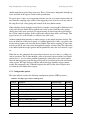
Abbreviations
TABLE 1.
Abbreviation
Explanation
AHB
Advanced High-performance Bus
AMBA
Advanced Microcontroller Bus Architecture
APB
Advanced Peripheral Bus
ASIC
Application Specific Integrated Circuit
BAR
Bank Address Register
DCL
Debug Communication Link
DSU
Debug Support Unit
EDA
Electronic Design Automation
FPGA
Field Programmable Gate Array
GDB
Gnu Debugger
GPL
Gnu Public License
GUI
Graphical User Interface
HDL
Hardware Description Language
IEEE
Institute of Electrical and Electronics Engineers
IP
Intellectual Property (in EDA context: reusable logic block)
ISA
Instruction Set Architecture
JTAG
Joint Test Action Group
MII
Media Independent Interface
OLA
On-chip Logic Analyzer
PCI
Peripheral Component Interconnect
RAM
Random Access M emory
SEU
Single Event Upset
SOC
System On Chip
SPARC V8
Scalable Processor ARChitecture Version 8
TCL
Tool Command Language
TCP
Transmission Control Protocol
UART
Universal Asynchronous Receiver Transmitter
VHDL
Very high speed integrated circuit Hardware Description Language
5
Design and implementation of an On-chip Logic Analyzer
Table of contents
1.0
Introduction ............................................................................................................. 8
2.0
GRLIB ..................................................................................................................... 9
2.1
2.2
3.0
The On-chip Logic Analyzer................................................................................. 15
3.1
3.2
3.3
4.0
Logic Analyzer configuration file ..................................................................................... 30
Logic Analyzer commands ............................................................................................... 31
The Value Change Dump format ...................................................................................... 32
Logic Analyzer GUI .............................................................................................. 35
5.1
6.0
Logic Analyzer fundamentals ........................................................................................... 15
Specification...................................................................................................................... 15
3.2.1
Overview............................................................................................................. 16
3.2.2
Operation ............................................................................................................ 16
3.2.3
Configuration options ......................................................................................... 17
3.2.4
Vendor and device id .......................................................................................... 18
3.2.5
Registers ............................................................................................................. 18
3.2.6
Trace buffer......................................................................................................... 21
3.2.7
Signal description ............................................................................................... 22
3.2.8
Library dependencies.......................................................................................... 22
3.2.9
On-chip Logic Analyzer instantiation ................................................................ 22
Implementation ................................................................................................................. 24
3.3.1
The two-process design method ......................................................................... 24
3.3.2
Clock domains .................................................................................................... 25
3.3.3
APB address mapping ........................................................................................ 26
3.3.4
Registers ............................................................................................................. 27
3.3.5
The trigger engine............................................................................................... 28
3.3.6
The trace buffer................................................................................................... 29
GRMON ................................................................................................................ 30
4.1
4.2
4.3
5.0
LEON3 .............................................................................................................................. 10
AMBA............................................................................................................................... 11
2.2.1
AHB.................................................................................................................... 11
2.2.2
APB .................................................................................................................... 12
The GDB Remote Serial Protocol..................................................................................... 36
Example traces....................................................................................................... 38
6.1
6.2
JTAG ................................................................................................................................. 38
Ethernet ............................................................................................................................. 40
7.0
Conclusions and discussion................................................................................... 42
8.0
References ............................................................................................................. 43
6
Design and implementation of an On-chip Logic Analyzer
Introduction
1.0 Introduction
As the complexity of hardware designs grows it gets harder and harder to verify the functionality of the circuit. Simulation has long been the only practical way of verifying ASIC
designs, but as it is now common with multi-million gate System on Chip designs this is
becoming an ever more time consuming task.
Luckily the FPGAs have grown in size and functionality as well, and are therefore commonly used for prototyping. With an FPGA you can run your system in real hardware
using live data for verification. This of course speeds up the development process.
Regardless of whether a design is prototyped using FPGAs or designed directly for FPGA
it is efficient to use their reprogrammability for debugging the hardware. Also some bugs
are very hard to find using simulation only. It might be that a very infrequent sequence of
data makes the design function incorrectly and that it is impossible to simulate the needed
amount of data for that sequence to occur. To find such errors the design must run in hardware.
The problem is the lack of visibility of the signals inside the FPGA. When simulating the
designer decides which nodes that are of interest and gets a waveform for each. Designs
are often very pin limited so there is no way to route the signals of interest to the pins of
the FPGA for probing with an external logic analyzer. The object of this Master’s thesis
has been to develop an On-chip Logic Analyzer (OLA) IP core that would bring the
debugging functionality of a normal logic analyzer inside the FPGA fabric. This development consisted of working out a specification and implementing it in VHDL. The OLA IP
core will be integrated into Gaisler Research’s GRLIB IP Library available under the GPL
license (also available under commercial licensing). A debug driver has also been written
for their proprietary GRMON debug monitor application so that the OLA can be controlled and configured using GRMON commands supplied by the driver. For even easier
configuration of the OLA a GUI front end was developed in tcl/tk. The debug driver can
dump the trace buffer to VCD-format files that can be viewed in e.g. the open source
GTKWave waveform viewer.
The work is described in this report and it begins in chapter 2 with some information about
the GRLIB library giving the basics of the environment in which the OLA will be used
and be a part of. In chapter 3 the specification of the hardware is presented and the implementation is described. Chapter 4 describes the functionality provided by the GRMON
debug driver. Due to the proprietary nature of GRMON this discussion will be on a level
that does not go into detail of the application structure. The GUI will be described in chapter 5 which is followed by some example traces in chapter 6 and then chapter 7 contains
conclusions and discussion. In the appendix the source code for the hardware and GUI can
be found.
7
Design and implementation of an On-chip Logic Analyzer
GRLIB
2.0 GRLIB
Since the On-chip Logic Analyzer will be integrated into the GRLIB library and used in
that environment this chapter is dedicated to giving a brief description of its most important aspects and features.
GRLIB is a set of reusable IP cores for System On-Chip design that is designed with the
following main goals [1]:
•
•
•
•
•
•
•
Common interfaces
Unified synthesis and simulation scripts
Built-in portability
Multi vendor support
CAD-tool independent
Open and extensible format
SEU tolerance for space applications
It is organized around VHDL-libraries and it provides automatic script generation for the
Modelsim, NCSim, and GHDL simulators and for the Synopsis, Synplify, Cadence, Xilinx
and Altera synthesis tools [2].
The IP library is bus-centric and is built around the AMBA 2.0 AHB/APB on-chip bus. It
includes numerous cores, for example the LEON3 SPARC V8 processor, IEEE 754 compliant FPU, memory controllers, PCI bridge, UART, timer and many more. The library is
designed so that it is easy for other vendors to include their own libraries.
8
Design and implementation of an On-chip Logic Analyzer
GRLIB
2.1 LEON3
LEON3 is a 32 bit highly configurable SPARC V8 [3] compliant synthesisable CPU. It is
developed in VHDL and is a part of the GRLIB IP library. It uses Harvard architecture
with configurable multiset caches and it implements the full SPARC V8 ISA including the
MUL, MAC and DIV instructions. An optional single/double precision FPU is also available.
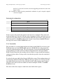
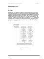
A more detailed description can be found in [4]. The figure below shows the different configurations of the LEON3 CPU.
FIGURE 1. LEON3 configuration blocks [4].
9
Design and implementation of an On-chip Logic Analyzer
GRLIB
2.2 AMBA
The Advanced Microcontroller Bus Architecture (AMBA) is a bus developed by the ARM
corporation. It is intended as an on-chip bus for high-performance embedded microcontrollers. It is used in GRLIB because of its market dominance, good documentation and
because it can be used for free without licensing restrictions [2]. Four key requirements of
the AMBA specification are [5]:
• Facilitate right-first-time development
• Technology independent
• Modular system design
• Minimize the silicon infrastructure
The AMBA specification has three different buses, the Advanced High-performance Bus
(AHB), the Advanced System Bus (ASB) and the Advanced Peripheral Bus (APB). In
GRLIB the AHB and APB are used. Adding IP cores to the AMBA buses are unfortunately not as flexible as one would wish and therefore some slight changes has been made
for the implementation in GRLIB. A decentralized address decoding scheme, interrupt
steering and device identification have been added using additional “side band” signals.
This makes it easy to design SoCs with plug & play capabilities.
2.2.1 AHB
AHB is the system bus for high-performance, high clock frequency designs and it is has
the following features required in such systems:
• burst transfers
• split transactions
• single-cycle bus master hand over
• single-clock edge operation
• non-tristate implementation
• wider data bus configurations (64/128 bits)
Normally an AHB design contains the following components: masters, slaves, an arbiter
and a decoder. Masters can initiate data transfer whilst slaves can only respond to the
requests from the masters. The arbiter selects which of the available masters that gets
access to the bus and the address decoder decodes the select signal from the address provided by the master.
10
Design and implementation of an On-chip Logic Analyzer
GRLIB
Since there are no tristate drivers the bus is multiplexed which is illustrated in the figure
below.
FIGURE 2. AHB interconnection view [2]
As mentioned the implementation of AHB in GRLIB also provides plug & play capabilities. Each AHB unit has a configuration record of eight 32-bit words. These words holds
information about the unit, its interrupt steering and address decoding of AHB slaves.
Since every slave provides its own address decoding information there is no need to modify the central decoder when a new slave is added. This configuration record is configured
by VHDL generics and is sent to the AHB controller which creates a table that is mapped
into the address space. A plug & play operation system can then read this table and determine which units that are attached and how they are configured. For a more detailed
description of this mechanism see [2].
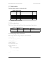
2.2.2 APB
APB has been optimized for low power consumption and reduced interface complexity.
Components that should fill those requirements and that don’t need the high bandwidth of
AHB is suitable for APB. The APB is connected to the AHB through an AHB slave acting
as a bridge between the two buses as seen in figure 3.
11
Design and implementation of an On-chip Logic Analyzer
GRLIB
FIGURE 3. Typical AMBA bus configuration [5]
For the On-chip Logic Analyzer there is no need of high performance since only register
control and trace buffer read out is done over the bus. The trace buffer can be quite large
but the read out is not time critical, so the choice of bus is APB.
The APB is also multiplexed as shown in figure 4.
FIGURE 4. APB interconnection view [2]
12
Design and implementation of an On-chip Logic Analyzer
GRLIB
An APB transfer always takes two bus cycles, called the setup and enable cycles. During
the setup cycle of a write operation the values of the address, pwrite, psel and data signals
are set. In the next bus cycle the enable signal goes high and the unit selected by psel shall
sample the data. The address, control and data are valid during the whole enable cycle. A
read operation has the same timing for all signals except the data. In the enable cycle of an
read operation the slave must provide the data which is then sampled by the master on the
rising edge of the clock that ends the enable cycle. This timing is illustrated in figure 5.
FIGURE 5. APB timing [5]
The GRLIB APB implementation provide plug & play information very much like previously described for AHB. Every APB slave has a two word configuration record. It consists of the identification register and the Bank Address Register (BAR). The identification
register holds information that identifies the slave and configures the interrupt steering.
The BAR defines the address decoding of the slave. See figure 6 for the layout of these
registers. APB slaves are addressed through the AHB address space. The 12 most significant bits of the AHB address decodes the AHB/APB bridge leaving 20 bits for all the APB
slaves on that bus. The 12 most significant bits that are left (i.e. bits 19-8) are compared
with the address field of the BAR only comparing the bits specified by the mask field of
the BAR. Thus a minimum address space of 256 bytes is occupied by each APB slave and
a maximum would use all the 20 bits, i.e. one MB of address space.
FIGURE 6. Plug & play configuration layout [2]
13
Design and implementation of an On-chip Logic Analyzer
The On-chip Logic Analyzer
3.0 The On-chip Logic Analyzer
3.1 Logic Analyzer fundamentals
The fundamental function of a logic analyzer is to sample a set of traced signals and to
detect events or a sequence of events in these signals. Upon detection of a user specified
event the logic analyzer triggers. When the sampling stops relative to the trigger is specified by the user. The common trigger modes are post trig, pre trig and center. In pre trig the
stored data set will consist of data sampled after the trigger. Post trig is the opposite and in
this mode the logic analyzer stops the sampling immediately when the trigger is raised
thus only storing data from before the triggering event. Center is a combination putting the
triggering event in the middle of the sampled data set.
There is a wide variety of logic analyzers available with different capabilities. The most
advanced can have hundreds of channels and advanced triggers which allows looping and
branching between triggering events. The sampled data can be viewed either in list form as
a list of values or as graphical waveforms.
Several vendors provide different commercial on-chip logic analyzers. For example Xilinx
has its Chipscope pro product and Altera’s counterpart is called Signaltap II. These are
highly configurable and support many different triggering capabilities. The drawback
mainly is that they can only be used with the companies respective products and that they
are integrated into the companies design tools. Since GRLIB is vendor and CAD-tool
independent the object of this thesis is to design an on-chip logic analyzer which can be
used independently of the devices and tools currently in use.
An important difference between a typical on-chip logic analyzer and a normal external
logic analyzer is that the on-chip logic analyzer will sample with the rate of the system
clock while an external logic analyzer uses a higher frequency sample rate and can therefore detect events occurring during the clock cycles. Glitches and timing problems are not
possible to observe using this on-chip logic analyzer running at system clock frequency.
3.2 Specification
The first part of this thesis work was to define the desired functionality of the On-chip
Logic Analyzer. The functionality was discussed with my supervisor, other logic analyzers
on the market was studied and a specification was written. When the specification was
agreed on the implementation in VHDL began. The implementation will be discussed further in the next chapter. At first the logic analyzer had only one clock domain, i.e. the trigger engine as well as the APB interface used the same clock. In a later design stage it was
decided to let the trigger engine use a separate clock so that it is possible to sample using
other clocks than the system clock. Below the final specification is presented.
14
Design and implementation of an On-chip Logic Analyzer
The On-chip Logic Analyzer
3.2.1 Overview
The logic analyzer was designed as an AMBA APB slave. Both the trace buffer and the
control registers are accessed through the APB address space. It supports multiple trigger
levels where each level has flexible settings enabling it to capture complex events. The
trace buffer is a circular buffer with configurable width and depth. The number of trig levels, the width and depth of the trace buffer as well as some other parameters described
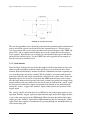
below are configured with VHDL generics. See figure 7 for a block diagram of the Onchip logic analyzer.
On-chip Logic Analyzer core
Traced
signals
Trigger engine
Trace buffer
On-chip RAM
Write port
Control unit with
APB slave interface
Read port
AMBA APB
FIGURE 7. On-chip Logic Analyzer block diagram
3.2.2 Operation
Each level is associated with a pattern and a mask. The traced signals are compared with
the pattern, only comparing the bits set in the mask. This allows for triggering on any specific value or range. Furthermore each level has a match counter and a boolean equality
flag. The equality flag specifies whether a match means that the pattern should equal the
traced signals or that it should not be equal. Its possible to configure the trigger engine to
stay at a certain level while the traced signals have a certain value using this flag. The
match counter is a 6 bit counter which can be used to specify how many times a level
15
Design and implementation of an On-chip Logic Analyzer
The On-chip Logic Analyzer
should match before proceeding to the next. This is all run-time configurable through registers described in the register section of this specification.
To specify post-, center- or pre triggering mode the user can set a counter register that controls when the sampling stops relative to the triggering event. It can be set to any value in
the range 0 to depth-1 thus giving total control of the trace buffer content.
When sampling slowly changing events like for example a uart it might be difficult to find
a bug since the trace buffer fills up with the rate of the system clock thus only giving a
short period of the uarts operation. To support tracing of such designs the logic analyzer
has a 16 bit sample frequency divider register that controls how often it will sample. This
register resets to 1 so the default is to sample every clock cycle.
Another configuration option has a similar purpose as the sample frequency divider. The
user can define one of the traced signals as a qualifier bit that has to have a specified value
for the current signals to be stored in the trace buffer. This makes sampling of larger time
periods possible if only some easily distinguished samples are interesting. This option has
to be enabled with the usequal generic and the qualifier bit and value are written to a register.
When the user has configured the logic analyzer the next step is to arm it, i.e telling it to
start its operation. This is done through a write to the status register with the least significant bit set to 1. A reset can be performed anytime by writing zero to the status register.
After the final triggering event the trigged flag will be raised and can be read out from the
status register. The logic analyzer remains armed and trigged until the trigger counter
reaches the configured value. When this happens the index of the oldest sample can be
read from the trace buffer index register.
3.2.3 Configuration options
The logic analyzer core has the following configuration options (VHDL generics):
TABLE 2. On-chip Logic Analyzer VHDL generics
16
Generic
Function
Allowed range
Default
dbits
Number of traced signals
1 - 256
32
depth
Number of stored samples
256 - 16384
1024
trigl
Number of trigger levels
1 - 63
1
usereg
Use input register
0-1
1
usequal
Use storage qualifier
0-1
0
pindex
APB slave index
0 - NAPBSLV - 1
0
paddr
The 12-bit MSB APB address
0 -16#FFF#
0
pmask
The APB address mask
16#000 - 16#F00#
F00
memtech
Memory technology
0 - NTECH
0
Design and implementation of an On-chip Logic Analyzer
The On-chip Logic Analyzer
The usereg generic specifies whether to use an input register to synchronize the traced signals and to minimize their fan out. If usereg=1 then all signals will be clocked into a register on the positive edge of the supplied clock signal, otherwise they are sent directly to the
RAM.
3.2.4 Vendor and device id
The module has vendor id 0x01 (Gaisler Research) and device id 0x060. For description
of vendor and device ids see GRLIB IP Library User’s Manual [2].
3.2.5 Registers
Table 67 shows the logic analyzer registers. Runtime configurations is done through these
registers which are mapped into the APB address space.
TABLE 3. Available registers
Registers
APB Address offset
Status register
0x00
Trace buffer index
0x04
Page register
0x08
Trig counter
0x0C
Sample freq. divider
0x10
Storage qualifier setting
0x14
Trig control settings
0x2000-0x203F
Pattern/mask configuration
0x6000-0x6FFF
Status register
31
usereg
30
qualifier
29
armed
28
trigged
27
dbits
20
19
depth
6
5
trig levels
0
FIGURE 8. Status register
[31:28] - These bits indicate whether an input register and/or storage qualifier is used and if
the Logic Analyzer is armed and/or trigged.
[27:20] - Number of traced signals.
[19:6] - Last index of trace buffer. Depth-1.
[5:0] - Number of trig levels.
17
Design and implementation of an On-chip Logic Analyzer
The On-chip Logic Analyzer
Trace buffer index
31
abits abits-1
“000...0”
0
the index of the oldest sample
FIGURE 9. Trace buffer index register
[31:abits] - Reserved.
[abits-1:0] - The index of the oldest sample in the buffer. abits is the number of bits needed
to represent the configured depth.
Note that this register is written by the trigger engine clock domain and thus needs to be
known stable when read out. Only when the ‘armed’ bit in the status register is zero is the
content of this register reliable.
Page register
4 3
31
0
current page
“000...0”
FIGURE 10. Page register
[31:4] - Reserved.
[3:0] - This register selects what page that will be used when reading from the trace buffer.
The trace buffer is organized into pages of 1024 samples. Each sample can be between 1
and 256 bits. If the depth of the buffer is more than 1024 the page register has to be used to
access the other pages. To access the i:th page the register should be set i (where i=0..15).
Trig counter
31
abits abits-1
“000...0”
0
trig counter value
FIGURE 11. Trig counter register
[31:abits] - Reserved.
[nbits-1:0] - Trig counter value. A counter is incremented by one for each stored sample after
the final triggering event and when it reaches the value stored in this register the
sampling stops. 0 means posttrig and depth-1 is pretrig. Any value in between can
be used.
18
Design and implementation of an On-chip Logic Analyzer
The On-chip Logic Analyzer
Sample frequency divider
31
16
15
0
“000...0”
divider value
FIGURE 12. Sample freq. divider register
[31:16] - Reserved.
[15:0] - A sample is stored on every i:th clock cycle where i is specified through this register.
This resets to 1 thus sampling occurs every cycle if not changed.
Storage qualifier
9
31
8
“000...0”
qualifier bit
1
val
0
FIGURE 13. Storage qualifier register
[31:9] - Reserved.
[8:1] - Which bit to use as qualifier.
[0] - Qualify storage if bit is 1/0.
Trig control registers
This memory area contains the registers that control when the trigger engine shall proceed
to the next level, i.e the match counter and a one bit field that specifies if it should trig on
equality or inequality. There are trigl words where each word is used like in the figure
below.
7
31
“000...0”
6
match counter
1
eq
0
FIGURE 14. Trigger control register
[31:7] - Reserved.
[6:1] - Match counter. A counter is increased with one on each match on the current level and
when it reaches the value stored in this register the trigger engine proceeds to the
19
Design and implementation of an On-chip Logic Analyzer
The On-chip Logic Analyzer
next level or if it is the last level it raises the trigged flag and starts the count of the
trigger counter.
[0] - Specifies if a match is that the pattern/mask combination is equal or inequal compared
to the traced signals.
Pattern/mask configuration
31
0x6xxx
0x6xxx
0x6020
0x6000
Mask
Pattern
0
Mask
Pattern
In these registers the pattern and mask for each trig level is configured. The pattern and
mask can contain up to 8 words (256 bits) each so a number of writes can be necessary to
specify just one pattern. They are stored with the LSB at the lowest address. The pattern of
the first trig level is at 0x6000 and the mask is located 8 words later at 0x6020. Then the
next trig levels starts at address 0x6040 and so on.
3.2.6 Trace buffer
The trace buffer is a circular buffer implemented with on-chip RAM. It uses the two-port
RAM generator core from GRLIB which generates a RAM with one read port and one
write port with independent clocks. The exact properties of the generated RAM depends
on the technology used but it will most likely be implemented in a dual-ported block
RAM. Circular means that after writing to the last address it wraps around and continues
writing to the first address. It keeps track of an index that specifies where the start/end of
the buffer is.
It is placed in the upper half of the allocated APB address range. If the configuration needs
more than the allocated 32 kB of the APB range the page register is used to page into the
trace buffer. Each stored word is dbits wide but 8 words of the memory range is always
allocated so the entries in the trace buffer are found at multiples of 0x20, i.e. 0x8000,
0x8020 and so on.
The index of the oldest sample is found in the trace buffer index register
20
Design and implementation of an On-chip Logic Analyzer
The On-chip Logic Analyzer
3.2.7 Signal description
The Logic Analyzer signals are described in table 4.
TABLE 4. LOGAN signals
Signal name
Type
Function
Active
RST
Input
Reset
Low
CLK
Input
System clock
-
TCLK
Input
Sample clock
-
APBI*
Input
APB slave input signals
-
APBO*
Output
APB slave output signals
-
SIGNALS
Input
Vector of traced signals
-
* See GRLIB IP Library users manual
3.2.8 Library dependencies
Table 5 shows libraries that should be used when instantiating a Logic Analyzer.
TABLE 5. Library dependencies
Library
Package
Imported unit(s)
Description
GRLIB
AMBA
Signals
AMBA signal definitions
GAISLER
MISC
Component
Component declaration
3.2.9 On-chip Logic Analyzer instantiation
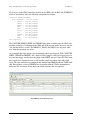
This examples shows how a Logic Analyzer can be instantiated.
library ieee;
use ieee.std_logic_1164.all;
library grlib;
use grlib.amba.all;
library gaisler;
use gaisler.misc.all;
entity logan_ex is
port (
clk : in std_ulogic;
rstn : in std_ulogic;
... -- other signals
);
end;
21
Design and implementation of an On-chip Logic Analyzer
The On-chip Logic Analyzer
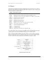
architecture rtl of logan_ex is
-- AMBA signals
signal apbi : apb_slv_in_type;
signal apbo : apb_slv_out_vector := (others => apb_none);
signal signals : std_logic_vector(64 downto 0);
begin
-- AMBA Components are instantiated here
...
-- Assign signals with the signals you want to trace
...
-- Logic analyzer core
logan0 : logan
generic map (dbits=>64,depth=>4096,trigl=>2,usereg=>1,usequal=>0,
pindex => 3, paddr => 3, pmask => 16#F00#, memtech => memtech)
port map (rstn, clk, clk, apbi, apbo(3), signals);
end;
22
Design and implementation of an On-chip Logic Analyzer
The On-chip Logic Analyzer
3.3 Implementation
When the specification was agreed on the next step was to implement it in VHDL. At
Gaisler Research they use a design style which they have worked out through long experience of hardware design and VHDL coding. It’s called the ‘two-process’ method and is
described below. A more thorough discussion of this method can be found in [6].
Some specific aspects of the implementation will be discussed as well in this chapter.
3.3.1 The two-process design method
The traditional VHDL design style is obviously influenced by the fact that before synthesis tools were commonly used digital hardware designers did their work using schematics
consisting of many components from a target library. This design style can be called the
dataflow style. Such VHDL code typically have a lot of small interconnected processes
where each process has the functionality of some component in the old school schematic.
The dataflow style easily becomes difficult to read and maintain. Furthermore the code
will simulate slower and will not make the best out of today’s advanced synthesis tools.
The two-process design style has been developed with the following goals:
• Provide uniform algorithm encoding
• Increase abstraction level
• Improve readability
• Clearly identify sequential logic
• Simplify debugging
• Improve simulation speed
• Provide one model for both synthesis and simulation
It reaches these goals with a quite simple scheme. The VHDL code of an entity is structured into only two processes. One containing all the combinatorial logic and one with
only sequential logic, as in figure 15.
23
Design and implementation of an On-chip Logic Analyzer
The On-chip Logic Analyzer
FIGURE 15. Two-process circuit
This way the algorithm can be coded using non concurrent statements in the combinatorial
process and all the registers can be inferred in the sequential process. The two-process
style also promotes the use of records and other more advanced features of the VHDL language. The r and rin signals from the figure above are the signals that ties the two processes together. Typically they are of record type and contain all the registers that will be
inferred in the clocked process. See the VHDL code in the appendix for an example of
how the two-process method is used.
3.3.2 Clock domains
Since the Logic Analyzer has two clocks that might be totally independent care has to be
taken to avoid metastability problems when signals have to cross between these clock
domains. Each clock domain is structured with one combinatorial and one sequential process according to the two-process method. The trace buffer is two-ported with the write
port being clocked by the sample clock and the read port by the system clock. All the configuration registers are of course written from the APB domain and may not be written
after the logic analyzer has been armed since they are then being read by the sample clock
domain. Likewise the trace buffer index may not be read out until after the ‘armed’ signal
has been lowered. Only three signals crossing the clock domains need synchronization,
namely the ‘armed’, ‘trigged’ and ‘finished’ signals which controls the operation of the
trigger engine.
The ‘armed’ signal is raised by the user via APB and is sent to the trigger engine to start
operation. Then the ‘trigged’ signal goes high when the logic analyzer has triggered and it
is sent to the status register in the APB domain. When operation has finished the trigger
engine raises the ‘finished’ signal and the APB domain responds by lowering the ‘armed’
signal. These three signals are synchronized by passing through two synchronization registers before being used.
24
Design and implementation of an On-chip Logic Analyzer
The On-chip Logic Analyzer
APB interface
clock domain
System clock
armed
trigged
finished
Trigger engine
clock domain
Sample clock
FIGURE 16. Signals needing synchronization
3.3.3 APB address mapping
The implementation work of the logic analyzer began with the layout of the address space.
There was going to be quite a lot of registers, especially the pattern/mask configuration
would be pretty large. Since it should be possible to have a 16k deep trace buffer where
each trace possibly takes 32 bytes the buffer could possibly be as large as 512 kB. So to
get by with only using 16 of the available 20 bits a paging register was introduced for
accessing the trace buffer. If using 16 bits in total and bit 4 downto 2 is used for selecting a
word in the (possibly 8 word big) trace, and the upper most bit is used for selecting the
trace buffer there are 10 bits left for selecting a specific trace. Thus every page holds 1024
traces and a maximum of 16 pages are used to hold the largest configuration.
If the MSB is low the registers are selected. They are divided into three categories and bit
14-13 selects between the categories pattern/mask, trigger control and miscellaneous.
Pattern/mask: apbi.paddr(14 downto 13) = “11”
In pattern/mask bit 11 downto 6 selects which trig level, bit 5 selects pattern (0) or mask
(1) and bit 4 downto 2 which word in the pattern/mask that is to be written or read.
Trigger control: apbi.paddr(14 downto 13) = “01”
When trigger control is selected bits 7 downto 2 selects which of the possible 64 trig levels
that are to be configured.
Miscellaneous: apbi.paddr(14 downto 13) = “00”
Here bit 4 downto 2 select between a number of different registers.
25
Design and implementation of an On-chip Logic Analyzer
“000”
“001”
“010”
“011”
“100”
“101”
-
The On-chip Logic Analyzer
status register
trace buffer index (read only)
page register
trigger counter
sample freq. divider
sample qualifier
3.3.4 Registers
The memory mapped registers whose addressing was described above are simply inferred
in the clocked processes by the assignment of rin to r where rin and r are of the same
record type which describes all the registers inferred by that process. The code below
defines the record types used in the logic analyzer design. Registers with the postfix
“_demet” are the first synchronization registers.
This first record defines the registers that are clocked by the system clock.
type reg_type is record
armed
: std_ulogic;
trig_demet : std_ulogic;
trigged
: std_ulogic;
fin_demet
: std_ulogic;
finished
: std_ulogic;
qualifier
: std_logic_vector(7 downto 0);
qual_val
: std_ulogic;
divcount
: std_logic_vector(15 downto 0);
counter
: std_logic_vector(abits-1 downto 0);
page
: std_logic_vector(3 downto 0);
trig_conf
: trig_cfg_arr;
end record;
The composite type trig_cfg_arr is an array of another record which is defined like this:
type trig_cfg_type is record
pattern : std_logic_vector(dbits-1 downto 0);
mask
: std_logic_vector(dbits-1 downto 0);
count
: std_logic_vector(5 downto 0);
eq
: std_ulogic;
end record;
The array thus contains the pattern and mask as well as the trigger control for every trig
level. This coding style makes it up to the synthesis tool whether to infer dist-ram or flipflops although flips-flops will be chosen with very high probability. There is usually no
gain in forcing the use of distributed RAM here because the width (pattern, mask, count
26
Design and implementation of an On-chip Logic Analyzer
The On-chip Logic Analyzer
and eq all concatenated) is so much larger than the depth so bits will most likely be
wasted.
The last record contains the registers clocked by the sample clock. Of these only w_addr is
memory mapped. The others are only used internally by the trigger engine.
type trace_reg_type is record
armed
: std_ulogic;
arm_demet
: std_ulogic;
trigged
: std_ulogic;
finished
: std_ulogic;
sample
: std_ulogic;
divcounter : std_logic_vector(15 downto 0);
match_count : std_logic_vector(5 downto 0);
counter
: std_logic_vector(abits-1 downto 0);
curr_tl
: integer range 0 to trigl-1;
w_addr
: std_logic_vector(abits-1 downto 0);
end record;
3.3.5 The trigger engine
When the logic analyzer has been armed it begins operation and starts to sample the traced
signals taking the configuration of qualifier and sample frequency divider into account.
The sample frequency divider is implemented as a counter that decreases by one every
clock cycle and when it reaches zero it is reloaded from the sample freq. divider register. If
the logic analyzer is configured to use a qualifier bit then every time this counter reaches
zero the qualifier bit is checked and if it has the configured value the ‘sample’ signal is
raised.
As long as the analyzer hasn’t been trigged the traced signals are compared with the pattern configured on the current trig level only comparing the bits set in the mask for that
trig level. This is done by checking if:
signals XOR pattern AND mask
equals zero. If it does equal zero the signals and the pattern was “equal”. Depending on
whether the logic analyzer is configured to trig on equality or inequality this counts as a
match. If the match counter for this trig level has reached the specified number the trigger
engine proceeds to the next trig level or if this was the last trig level it raises the ‘trigged’
signal. If the match counter has not reached the specified number it is increased and the
logic analyzer keeps looking for more matches on this level.
When the logic analyzer has been trigged it starts to count up the trigger counter. It is
increased by one every time a sample is taken when the engine is in its ‘trigged’ state.
When it reaches the value written to the trigger counter register the ‘trigged’ signal is
27
Design and implementation of an On-chip Logic Analyzer
The On-chip Logic Analyzer
cleared thus ending the sampling and the ‘finished’ signal is raised. When the ‘finished’
signal has been synchronized in the system clock domain the ‘armed’ signal is cleared
which in turn pulls down the ‘finished’ signal so that the logic analyzer is left in an idle
state.
The last written index + 1, i.e. the index of the oldest sample can be read out of the trace
buffer index register.
3.3.6 The trace buffer
The trace buffer is implemented with on-chip ram using the two port synchronous RAM
generator available in GRLIB. The RAM is instantiated to be as wide as the number of
traced signals and as deep as the configured depth of the trace buffer.
The read port is addressed with the 10 bits from the APB address that specify a certain
trace. If more than 10 bits are needed the additional bits are concatenated from the 4-bit
page register. The number of bits needed to address the trace buffer is calculated using a
log2 look-up table (provided by GRLIB). For example if the trace buffer is 4096 deep 12
bits will be needed and only 2 bits of the page register will be used. The log2 look-up table
has 64 entries thus limiting the address range to cover 6 powers of 2. A range from 256 to
16384 was chosen. The read enable signal is set if an address belonging to the trace buffer
is being read. Which word in the trace delivered from the RAM that is to be sent out on the
bus is multiplexed using the APB address bits as described previously.
Every time a trace is to be written to the buffer the sample signal in the register is set. This
signal is used as write enable, so the current trace is always clocked into another register
holding the “old” trace which is the one written to the write port of the RAM when the
sample signal is high. The address used by the write port is a counter that is increased
every time a trace has been written to the buffer. This counter is memory mapped as
described previously.
28
Design and implementation of an On-chip Logic Analyzer
GRMON
4.0 GRMON
GRMON is a general debug monitor for the systems developed by Gaisler Research. It has
the following back-ends defining its behavior:
• LEON2 simulator
• LEON2 Debug Support Unit (DSU)
• GRLIB DSU (for SOC designs based on GRLIB)
• GRLIB simulator
The user interface (front-end) is common for all back ends and it passes commands
entered by the user to the back-end which executes them. GRMON includes the features
listed below [7]
• Read/write access to all LEON registers and memory
• Built-in disassembler and trace buffer management
• Downloading and execution of LEON applications
• Breakpoint and watchpoint management
• Remote connection to GNU debugger (gdb)
Connection from GRMON to a design can be done through any on-chip AHB master with
a communication module. For the GRLIB back-end the currently available debug communication links (DCL) are serial port (UART), JTAG, ethernet, and PCI. The operation of
the different DCLs are the same but of course the bit rate varies.
The added plug & play capabilities of the GRLIB AMBA interface makes it possible for
GRMON to identify which IP cores that are configured in the design. For each core a
debug driver is loaded which provides initialisation and core specific commands. Such a
driver has been developed for the On-chip Logic Analyzer IP core and it will be integrated
into GRMON. Users can also create their own debug drivers for their cores using loadable
modules.
4.1 Logic Analyzer configuration file
To be able to identify the different signals that make up the pattern the user has to enter the
signal names and sizes in a text file named setup.logan. This file is read by the debug
driver so that it can interpret the pattern and display the correct values along with the name
for each signal. An entry in the file consists of a signal name followed by its size in bits
separated by whitespace. Rows not having these two entries as well as rows beginning
with an # are ignored.
29
Design and implementation of an On-chip Logic Analyzer
GRMON
Example:
count31_16 16
count15_6 10
count5_0 6
This configuration has a total of 32 traced signals and they will be displayed as three different signals being 16, 10 and 6 bits wide. The first signal in the configuration file maps to
the most significant bits of the vector with the traced signals.
4.2 Logic Analyzer commands
This section describes the commands provided by logic analyzer debug driver. All logic
analyzer commands are prefixed with “la”. For example, to dump the trace buffer you
enter “la dump [file]” where [file] is an optional filename. Common for all commands that
sets a register is that if the value is not specified the current setting is displayed. If the trig
level is left out the command displays the current setting for all trig levels.
TABLE 6.
la status
Reports status of logan (equivalent with writing just la).
la arm
Arms the logan. Begins the operation of the analyzer and sampling starts.
la reset
Stop the operation of the logan. Logic Analyzer returns to idle state.
la pm [trig level] [pattern] [mask]
Sets/displays the complete pattern and mask of the specified trig level. If not fully
specified the input is zero-padded from the left. Note: Decimal notation only possible for widths less than or equal to 64 bits.
la pat [trig level] [bit] [0 | 1]
Sets/displays the specified bit in the pattern of the specified trig level to 0/1.
la mask [trig level] [bit] [0 | 1]
Sets/displays the specified bit in the mask of the specified trig level to 0/1.
la trigctrl [trig level] [match counter] [trig condition]
Sets/displays the match counter and the trigger condition (1 = trig on equal, 0 = trig
on inequal) for the specified trig level.
la count [value]
Set/displays the trigger counter. The value should be between zero and depth-1 and
specifies how many samples that should be taken after the triggering event.
30
Design and implementation of an On-chip Logic Analyzer
GRMON
TABLE 6.
la div [value]
Sets/displays the sample frequency divider register. If you specify e.g. “la div 5” the
logic analyzer will only sample a value every 5th clock cycle.
la qual [bit] [value]
Sets/displays which bit in the sampled pattern that will be used as qualifier and what
value it shall have for a sample to be stored.
la dump [filename]
This dumps the trace buffer in VCD format to the file specified (default is log.vcd).
la view [start index] [stop index] [filename]
Prints the specified range of the trace buffer in list format. If no filename is specified
the commands prints to the screen.
la page [page]
Sets/prints the page register of the logan. Normally the user doesn’t have to be concerned with this because dump and view sets the page automatically. Only useful if
accessing the trace buffer manually via the grmon mem command
4.3 The Value Change Dump format
Value Change Dump (VCD) is a format defined by the Verilog IEEE 1364 standard. It is a
file format for waveforms and can be generated by many HDL simulators. Since it is an
open format and largely supported this is the format used by the Logic Analyzer debug
driver in GRMON when creating dump files. Most commercial waveform viewers can
import this format and there are at least two open source viewers, GTKWave and
Dinotrace. Both have been used for opening VCD-files generated by the driver with good
results.
The format is not described in detail in this report. For the complete specification the
reader is referred to the IEEE 1364-2001 standard [8]. Below is a description of the parts
of the format needed and used by the logic analyzer driver.
VCD files are text files and use whitespace to separate keywords. The file starts with
header information giving the date of the file, the version of the software that created it
and the time scale used. After the header information the variables are defined and the rest
of the file contains timestamps and information about which variables changed and to
what values.
A typical entry in the VCD file looks like this:
$keyword <keyword dependent data> $end
31
Design and implementation of an On-chip Logic Analyzer
GRMON
The date, version and timescale keywords gives the header information as in the example
below:
$date 2005-05-25 $end
$version
On-chip Logic Analyzer waveform generator v1.0
$end
$timescale 1 ns $end
Variable definition is done using the var keyword. A variable definition follows this format: $var <width> <type> <identifier> <name> $end where width is the number of bits,
type is the type of the variable, identifier is a string of printable ASCII characters that will
represent the variable in the VCD file and name is a string that will appear in the waveform viewer. The type may be one of several different types for example integer, real, reg
and wire. Only wire is used in the VCD-files generated by the driver.
Initial values for all the variables are given with the $dumpvars command. Then each time
a variable changes value a timestamp is used followed by all the variable changes that
occurred in that time. Timestamps are indicated with a # followed by the time. Below is an
example of three variable definitions followed by a few value changes.
$var 1 wire ! clk $end
$var 8 wire 1 addr $end
$var 8 wire 2 data $end
#0
$dumpvars
1!
b00000000 1
b00000000 2
$end
#5
0!
#10
1!
b00000001 1
b10101010 2
#15
0!
#20
1!
b00000010 1
32
Design and implementation of an On-chip Logic Analyzer
GRMON
b11110000 2
#25
0!
Note that scalar variables can not have any space between their value and the identifier but
with vectors a space is required. The above example also shows how the sample clock
waveform is reconstructed. Since it is not possible to correctly sample any signal with a
higher frequency than half the sample frequency the clock signal obviously cannot be
sampled. Instead a sort of “virtual” clock signal is created which goes through a cycle with
every sample in the trace buffer. This equals the actual clock for traces where no qualifier
bit has been used and when the sampling frequency equals the clock frequency. If a qualifier is used then the time information goes away completely and therefore the user has to
connect a timer to the traced signals if time is of interest.
33
Design and implementation of an On-chip Logic Analyzer
Logic Analyzer GUI
5.0 Logic Analyzer GUI
It is quite easy to configure the logic analyzer using GRMON. But when there are many
traced signals keeping track of the patterns and masks can be a bit of a struggle. For making the configuration even easier a graphical user interface (GUI) was developed. Several
approaches were contemplated. Previous GUI’s for GRMON had used redirection of the
stdin and stdout IO streams to communicate. This was deemed as an unsatisfactory solution since it doesn’t go well with changes to GRMON. The solution was to use the gdb
remote debugging interface built into GRMON. This interface allows amongst other
things reads and writes to memory and the execution of any GRMON command. To use it
one have to initiate the interface using the gdb command which sets up tcp port 2222 for
incoming connections. The GDB remote serial protocol is then used for communication.
Another question was how the graphical user interface should be built, i.e. whether for
example GTK, Eclipse or tcl/tk should be used. The final decision was in favor of tcl/tk
because of its simplicity and rapid GUI development capabilities.
Figure 17 shows the final look of the GUI.
FIGURE 17. The Logic Analyzer GUI
34
Design and implementation of an On-chip Logic Analyzer
Logic Analyzer GUI
The left side has the settings for the different trig levels, i.e. pattern, mask, match counter
and trigger condition. Which trig level the settings apply to is chosen from an option
menu. The “Download conf” button transfers the values to the on-chip logic analyzer. The
pattern and mask is padded with zeroes from the left if not fully specified. They can be
entered either in hexadecimal or decimal but there is a limitation that no signal can be
wider than 64 bits. This is simply because tcl can not handle larger numbers without
extensions. In the hexadecimal case it would be quite simple to parse arbitrarily large
numbers in the same way that is done in the GRMON driver but since this limitation is not
that severe this has not been implemented in the GUI.
On the right side the status is shown and beneath are the settings which control the trace
buffer. These settings are sent to the logic analyzer when the user presses enter. The
‘armed’ and ‘trigged’ fields of the status can be reread by pressing the “Update status”
button.
There are also buttons to arm and reset the logic analyzer as well as to dump the vcd-file
and launch GTKWave. Any GRMON command can be issued from the entry below these
buttons.
From the file menu the current configuration can be saved and a new one can be loaded.
The GUI defaults to the same configuration file as the GRMON debug driver. If the configuration is saved it adds information about the setup which is ignored by GRMON. When
saving/loading any filename may be specified but during startup the GUI reads the
“setup.logan” file. Only files previously saved by the GUI can be loaded from this menu
option because it expects the additional information added by the GUI.
5.1 The GDB Remote Serial Protocol
The Gnu Debugger (GDB) can be used to debug remote targets, such as processors running in embedded systems. The processor has to have a communication link through
which it can communicate with gdb and a small piece of code, called a gdb stub, that acts
as the intermediate between gdb and the debugged system. GDB and the stub communicate with the GDB Remote Serial Protocol (RSP) which is an ASCII based protocol. For
debugging LEON systems GRMON can act as the remote end to which GDB connects,
and this way no stub has to be inserted into the code. GDB connects to tcp port 2222 on
the host running GRMON and then the commands issued are performed by GRMON
which communicates with the target hardware.
The On-Chip Logic Analyzer GUI uses this feature of GRMON to configure and check
the status of the logic analyzer hardware. Below is a description of the protocol.
Commands and responses are sent as packets where each packet looks like this:
$data#checksum
35
Design and implementation of an On-chip Logic Analyzer
Logic Analyzer GUI
The data part is either a command or a response. The checksum is a one byte checksum
calculated as the modulo 256 sum of all the characters between the leading $and the trailing #. Each sent packet has to be acknowledged either with a ‘+’ if the packet was received
correctly or with a ‘-’ if it was incorrect.
In this section the GDB RSP commands used by the GUI are explained. There are many
more and for a full description the reader is referred to [9].
Read memory: the ‘m’ command has the following syntax:
maddr, length
and the response is either the read bytes or an error code.
General query: the ‘q’ commands has the following syntax:
qquery
The general query command can be used to query the target about many different things.
A number of predefined queries exist and one of them is used by the GUI, namely the
qRcmd command which syntax is as follows:
qRcmd,command
The command, which must be hex encoded, is passed to the local interpreter, in this case
GRMON which executes it as an internal command. The response can either be OK if the
command has no output, a hex encoded output string or an error code if the command was
badly formed. A number of intermediate console output responses of the form Ooutput
can be sent from the target before the final response.
Detach:
D
This notifies the remote system that GDB detaches (or in this case the GUI). When
detached GRMON stops listening for incoming connections and can be used as normal.
The read memory command is used for reading the status word. All configuration is done
with the qRmcd command using the logic analyzer commands implemented in GRMON.
Detaching is done upon exit but can also be issued anytime from the file menu. There is
also a reconnect option under the file menu for establishing the connection to GRMON
again. Note that the gdb command must be issued in GRMON before it is possible to connect.
36
Design and implementation of an On-chip Logic Analyzer
Example traces
6.0 Example traces
6.1 JTAG
During testing of the On-chip Logic Analyzer a Xilinx Spartan-3 board has been used.
This device has dedicated JTAG pins which are connected to a JTAG controller circuit.
Through this circuit the device can be configured and internal boundary scan chains can be
defined. The JTAG interface consists of four signals, TMS, TCK, TDI and TDO (and
sometimes an optional reset signal TRST is used). TCK is the JTAG clock signal. The
value of the Test Mode Select (TMS) signal at every rising edge of TCK determines the
state of the JTAG state machine. In the SHIFT state the TDI and TDO pins are used to
shift in and out bits to and from the data or instruction register. The following diagram
shows how the JTAG FSM works:
FIGURE 18. JTAG FSM
37
Design and implementation of an On-chip Logic Analyzer
Example traces
To get access to the JTAG controller circuit from the HDL code the BSCAN_SPARTAN3
macro is instantiated. It has the following component declaration:
component BSCAN_SPARTAN3
port (CAPTURE : out STD_ULOGIC;
DRCK1 : out STD_ULOGIC;
DRCK2 : out STD_ULOGIC;
RESET : out STD_ULOGIC;
SEL1
: out STD_ULOGIC;
SEL2
: out STD_ULOGIC;
SHIFT : out STD_ULOGIC;
TDI
: out STD_ULOGIC;
UPDATE : out STD_ULOGIC;
TD01
: in STD_ULOGIC;
TD02
: in STD_ULOGIC);
end component;
The CAPTURE, RESET, SHIFT and UPDATE pins shows in which state the JTAG state
machine currently is. Unfortunately the TMS and TCK pins can not be observed, only the
state and the indata is visible. The DRCK1/2, TDO1/2 and SEL1/2 are only used when
user defined instructions are active.
As an example the logic analyzer was instantiated with 5 traced signals (TDI, CAPTURE,
SHIFT, UPDATE and RESET) and a depth of 16384 samples. Only one trigger level was
used and the trigger was the first rising edge of the SHIFT state pin. Since the JTAG interface is quite slow compared to the system clock a sample was taken every fifth clock
cycle. The logic analyzer was configured and armed using GRMON with the UART backend. Then another session of GRMON was started but with the JTAG communication
back-end. The waveforms below shows the initial sequence that was sampled.
FIGURE 19. JTAG interface trace
38
Design and implementation of an On-chip Logic Analyzer
Example traces
6.2 Ethernet
To demonstrate sampling using another clock than the system clock a trace was taken of
the Ethernet Media Independent Interface (MII) with its transmitter clock as sample clock.
The traced signals are shown in table 7.
TABLE 7. Sampled Ethernet signals
Signal
Description
TX_EN
Indicates that the data on TXD should be sampled by the PHY next cycle
TX_ER
If TX_ER is asserted at the same time as TX_EN it forces the PHY to send invalid data
TXD(3:0)
The nibble that shall be transmitted
RX_COL
High if a collision has occurred
RX_CRS
High if the medium is being used
RX_DV
High when received data is valid
RX_ER
High if an receive error has occurred and received data is invalid
RXD(3:0)
Received nibble. Synchronous to the RX_CLK
MDC
Clock for the management interface
MDIO_I
Configuration input
MDIO_O
Configuration output
MDIO_OE
Output enable for the bidirectional configuration signal
TX_CLK and RX_CLK are generated by the PHY. TX_EN, TX_ER, TXD and the management signals are driven by the Ethernet Media Access Controller (MAC).
Figure 18 shows the Ethernet MAC frame format. These are the actual bits sent on the
physical medium and consists of an Ethernet packet, the start of frame delimiter (SFD),
and the preamble. For detailed information on the Ethernet standard see [10]
FIGURE 20. Ethernet MAC frame
39
Design and implementation of an On-chip Logic Analyzer
Example traces
In this example the logic analyzer was set to trig on the first occurrence of TX_EN = ‘1’ so
the first transmission from the system is captured. Data is sent one nibble at a time starting
from the LSB of each octet. The preamble and the SFD are used for synchronizing the
receiver and the transmitter and they are seen in figure 19 below as the long sequence of
5’s followed by “D5” (although here in reverse order since LSB first). After that comes the
destination address which is 00:05:5D:96:07:62.
FIGURE 21. Ethernet MII trace, part 1
FIGURE 22. Ethernet MII trace, part 2
Next the source address 00:00:7A:CC:0:01 is sent as seen in figure 22 followed by the
type field, here “0x0608” specifying the ARP protocol. The rest of the data seen is from
the ARP packet but will not be described here.
40
Design and implementation of an On-chip Logic Analyzer
Conclusions and discussion
7.0 Conclusions and discussion
The object of this master’s thesis was to develop an On-Chip Logic Analyzer that could
trace arbitrary signals inside an FPGA and trig on complex events. The read out should be
done over the AMBA APB interface and functionality for the core was to be integrated
into the GRMON debug monitor.
An IP core that fulfills these requirements has been successfully implemented and tested.
The GRMON debug driver developed gives control of all configurability of the IP core
and can dump the trace buffer to VCD-format or list form. In addition to the original
requirements a GUI has been developed that makes configuration easier when many signals are to be traced.
Several test traces have been made and both the hardware and software functions as supposed. During the development and testing some ideas of improvement has been thought
of. For example it should be fairly simple to add support in the software for using multiple
Logic Analyzer cores in a design. This would be very handy if one wants to sample different clock domains.
41
Design and implementation of an On-chip Logic Analyzer
References
8.0 References
1. Gaisler, J. A Dual-Use Open-Source VHDL IP Library. Proceedings of the MAPLD
International Conference 2004, Sept. 8-10, Washington D.C, 2004.
2. Gaisler J, Habinc S, Catovic E. GRLIB IP Library User’s Manual, 2005 (available from
http://www.gaisler.com/products/grlib/docs/doc/grlib/grlib.pdf)
3. The SPARC Architecture Manual version 8, Upper sadle river NJ, Prentice Hall, 1992,
ISBN 0138250014
4. Leon 3/GRLIB Product Brief (available from: http://www.gaisler.com/doc/Leon3 Grlib
folder.pdf)
5. AMBA 2.0 Specification rev 2.0, 1999 (available from http://www.gaisler.com/doc/
amba.pdf)
6. Gaisler, J. A structured VHDL design model, (available from http://www.gaisler.com/
doc/vhdl2proc.pdf)
7. GRMON User’s Manual, May 27 2005 (available from http://www.gaisler.com/doc/
grmon-1.0.12.pdf)
8. IEEE 1364.1-2002, IEEE Standard for Verilog Register Transfer Level Synthesis, 2002,
ISBN 0-7381-3502-X.
9. Debugging with GDB, Free Software Foundation, Inc. (available from http://
sources.redhat.com/gdb/download/onlinedocs/gdb.html)
10. IEEE 802.3-2002, IEEE Standard for Telecommunications and Information exchange
between systems: Local and Metropolitan Area Networks: Carrier Sense Multiple Access
with Collision Detection (CSMA/CD) Access Method and Physical Layer Specifications.
2002; (available from: http://www.standards.ieee.org/getieee802/download/802.32002_part3.pdf)
42
Design and implementation of an On-chip Logic Analyzer
Appendix A -VHDL source code
------------------------------------------------------------------------------ Entity: logan_core
-- File:logan_core.vhd
-- Author:Kristoffer Carlsson
-- Description:On-chip logic analyzer IP core
----------------------------------------------------------------------------library ieee;
use ieee.std_logic_1164.all;
library grlib;
use grlib.amba.all;
use grlib.stdlib.all;
library gaisler;
use gaisler.devices.all;
use gaisler.memory.all;
entity logan is
generic (
dbits
: integer range 0 to 256 := 32;
depth
: integer range 256 to 16384 := 1024;
trigl
: integer range 1 to 63 := 1;
usereg
: integer range 0 to 1 := 1;
usequal : integer range 0 to 1 := 0;
pindex
paddr
pmask
memtech
port (
rstn
clk
tclk
apbi
apbo
signals
end logan;
:
:
:
:
integer
integer
integer
integer
:
:
:
:
:
:
in
in
in
in
out
in
:=
:=
:=
:=
-- Number of traced signals
-- Depth of trace buffer
-- Number of trigger levels
-- Use input register
-- Use qualifer bit
0;
0;
16#F00#;
0);
std_logic;
std_logic;
std_logic;
apb_slv_in_type;
apb_slv_out_type;
std_logic_vector(dbits - 1 downto 0));
-------
Synchronous reset
System clock
Trace clock
APB in record
APB out record
Traced signals
architecture rtl of logan is
constant REVISION : amba_version_type := 0;
constant pconfig : apb_config_type := (
0 => ahb_device_reg ( VENDOR_GAISLER, GAISLER_LOGAN, 0, REVISION, 0),
1 => apb_iobar(paddr, pmask));
constant abits: integer := 8 + log2x(depth/256 - 1);
constant az
: std_logic_vector(abits-1 downto 0) := (others => ‘0’);
constant dz
: std_logic_vector(dbits-1 downto 0) := (others => ‘0’);
43
Design and implementation of an On-chip Logic Analyzer
type trig_cfg_type is record
pattern : std_logic_vector(dbits-1 downto 0);
mask
: std_logic_vector(dbits-1 downto 0);
count
: std_logic_vector(5 downto 0);
eq
: std_ulogic;
-end record;
-- Pattern to trig on
-- trigger mask
-- match counter
Trig on match or no match?
type trig_cfg_arr is array (0 to trigl-1) of trig_cfg_type;
type reg_type is
armed
trig_demet
trigged
fin_demet
finished
qualifier
qual_val
divcount
counter
page
trig_conf
end record;
record
: std_ulogic;
: std_ulogic;
: std_ulogic;
: std_ulogic;
: std_ulogic;
: std_logic_vector(7 downto 0);
: std_ulogic;
: std_logic_vector(15 downto 0);
: std_logic_vector(abits-1 downto 0);
: std_logic_vector(3 downto 0);
: trig_cfg_arr;
type trace_reg_type is record
armed
: std_ulogic;
arm_demet
: std_ulogic;
trigged
: std_ulogic;
finished
: std_ulogic;
sample
: std_ulogic;
divcounter : std_logic_vector(15 downto 0);
match_count : std_logic_vector(5 downto 0);
counter
: std_logic_vector(abits-1 downto 0);
curr_tl
: integer range 0 to trigl-1;
w_addr
: std_logic_vector(abits-1 downto 0);
end record;
signal
signal
signal
signal
signal
signal
signal
r_addr
bufout
r_en
r, rin
tr, trin
sigreg
sigold
:
:
:
:
:
:
:
std_logic_vector(13 downto 0);
std_logic_vector(255 downto 0);
std_ulogic;
reg_type;
trace_reg_type;
std_logic_vector(dbits-1 downto 0);
std_logic_vector(dbits-1 downto 0);
begin
bufout(255 downto dbits) <= (others => ‘0’);
-- Combinatorial process for AMBA clock domain
comb1: process(rstn, apbi, r, tr, bufout)
variable
variable
variable
variable
44
v
rdata
tl
pattern, mask
:
:
:
:
reg_type;
std_logic_vector(31 downto 0);
integer range 0 to trigl-1;
std_logic_vector(255 downto 0);
Design and implementation of an On-chip Logic Analyzer
begin
v := r;
rdata := (others => ‘0’); tl := 0;
pattern := (others => ‘0’); mask := (others => ‘0’);
-- Two stage synch
v.trig_demet := tr.trigged;
v.trigged := r.trig_demet;
v.fin_demet := tr.finished;
v.finished := r.fin_demet;
if r.finished = ‘1’ then
v.armed := ‘0’;
end if;
r_en <= ‘0’;
-- Read/Write -if apbi.penable = ‘1’
and apbi.psel(pindex) = ‘1’ then
-- Write
if apbi.pwrite = ‘1’ then
-- Only conf area writeable
if apbi.paddr(15) = ‘0’ then
-- pattern/mask
if apbi.paddr(14 downto 13) = “11” then
tl
pattern(dbits-1 downto 0)
mask(dbits-1 downto 0)
:= conv_integer(apbi.paddr(11 downto 6));
:= v.trig_conf(tl).pattern;
:= v.trig_conf(tl).mask;
case apbi.paddr(5 downto 2) is
when
when
when
when
when
when
when
when
“0000”
“0001”
“0010”
“0011”
“0100”
“0101”
“0110”
“0111”
=>
=>
=>
=>
=>
=>
=>
=>
pattern(31 downto 0)
pattern(63 downto 32)
pattern(95 downto 64)
pattern(127 downto 96)
pattern(159 downto 128)
pattern(191 downto 160)
pattern(223 downto 192)
pattern(255 downto 224)
:=
:=
:=
:=
:=
:=
:=
:=
apbi.pwdata;
apbi.pwdata;
apbi.pwdata;
apbi.pwdata;
apbi.pwdata;
apbi.pwdata;
apbi.pwdata;
apbi.pwdata;
when
when
when
when
when
when
when
when
“1000”
“1001”
“1010”
“1011”
“1100”
“1101”
“1110”
“1111”
=>
=>
=>
=>
=>
=>
=>
=>
mask(31 downto 0)
mask(63 downto 32)
mask(95 downto 64)
mask(127 downto 96)
mask(159 downto 128)
mask(191 downto 160)
mask(223 downto 192)
mask(255 downto 224)
:=
:=
:=
:=
:=
:=
:=
:=
apbi.pwdata;
apbi.pwdata;
apbi.pwdata;
apbi.pwdata;
apbi.pwdata;
apbi.pwdata;
apbi.pwdata;
apbi.pwdata;
when others => null;
45
Design and implementation of an On-chip Logic Analyzer
end case;
-- write back updated pattern/mask
v.trig_conf(tl).pattern := pattern(dbits-1 downto 0);
v.trig_conf(tl).mask
:= mask(dbits-1 downto 0);
-- count/eq
elsif apbi.paddr(14 downto 13) = “01” then
tl
:= conv_integer(apbi.paddr(7 downto 2));
v.trig_conf(tl).count
:= apbi.pwdata(6 downto 1);
v.trig_conf(tl).eq
:= apbi.pwdata(0);
-- arm/reset
elsif apbi.paddr(14 downto 13)&apbi.paddr(4 downto 2) = “00000” then
v.armed := apbi.pwdata(0);
-- Page reg
elsif apbi.paddr(14 downto 13)&apbi.paddr(4 downto 2) = “00010” then
v.page := apbi.pwdata(3 downto 0);
-- Trigger counter
elsif apbi.paddr(14 downto 13)&apbi.paddr(4 downto 2) = “00011” then
v.counter := apbi.pwdata(abits-1 downto 0);
-- div count
elsif apbi.paddr(14 downto 13)&apbi.paddr(4 downto 2) = “00100” then
v.divcount := apbi.pwdata(15 downto 0);
-- qualifier bit
elsif apbi.paddr(14 downto 13)&apbi.paddr(4 downto 2) = “00101” then
v.qualifier := apbi.pwdata(7 downto 0);
v.qual_val := apbi.pwdata(8);
end if;
end if;
-- end write
-- Read
else
-- Read config/status area
if apbi.paddr(15) = ‘0’ then
-- pattern/mask
if apbi.paddr(14 downto 13) = “11” then
tl
pattern(dbits-1 downto 0)
mask(dbits-1 downto 0)
case apbi.paddr(5 downto
when “0000” => rdata
when “0001” => rdata
when “0010” => rdata
when “0011” => rdata
46
:= conv_integer(apbi.paddr(11 downto 6));
:= v.trig_conf(tl).pattern;
:= v.trig_conf(tl).mask;
2)
:=
:=
:=
:=
is
pattern(31 downto 0);
pattern(63 downto 32);
pattern(95 downto 64);
pattern(127 downto 96);
Design and implementation of an On-chip Logic Analyzer
when
when
when
when
“0100”
“0101”
“0110”
“0111”
=>
=>
=>
=>
rdata
rdata
rdata
rdata
:=
:=
:=
:=
pattern(159
pattern(191
pattern(223
pattern(255
when
when
when
when
when
when
when
when
“1000”
“1001”
“1010”
“1011”
“1100”
“1101”
“1110”
“1111”
=>
=>
=>
=>
=>
=>
=>
=>
rdata
rdata
rdata
rdata
rdata
rdata
rdata
rdata
:=
:=
:=
:=
:=
:=
:=
:=
mask(31 downto 0);
mask(63 downto 32);
mask(95 downto 64);
mask(127 downto 96);
mask(159 downto 128);
mask(191 downto 160);
mask(223 downto 192);
mask(255 downto 224);
when others => rdata
end case;
downto
downto
downto
downto
128);
160);
192);
224);
:= (others => ‘0’);
-- count/eq
elsif apbi.paddr(14 downto 13) = “01” then
tl
:= conv_integer(apbi.paddr(7 downto 2));
rdata(6 downto 1)
:= v.trig_conf(tl).count;
rdata(0)
:= v.trig_conf(tl).eq;
-- status
elsif apbi.paddr(14 downto 13)&apbi.paddr(4 downto 2) = “00000” then
rdata := conv_std_logic_vector(usereg,1) &
conv_std_logic_vector(usequal,1) &
r.armed & r.trigged &
conv_std_logic_vector(dbits,8)&
conv_std_logic_vector(depth-1,14)&
conv_std_logic_vector(trigl,6);
-- trace buffer index
elsif apbi.paddr(14 downto 13)&apbi.paddr(4 downto 2) = “00001” then
rdata(abits-1 downto 0) := tr.w_addr(abits-1 downto 0);
-- page reg
elsif apbi.paddr(14 downto 13)&apbi.paddr(4 downto 2) = “00010” then
rdata(3 downto 0) := r.page;
-- trigger counter
elsif apbi.paddr(14 downto 13)&apbi.paddr(4 downto 2) = “00011” then
rdata(abits-1 downto 0) := r.counter;
-- divcount
elsif apbi.paddr(14 downto 13)&apbi.paddr(4 downto 2) = “00100” then
rdata(15 downto 0) := r.divcount;
-- qualifier
elsif apbi.paddr(14 downto 13)&apbi.paddr(4 downto 2) = “00101” then
rdata(7 downto 0) := r.qualifier;
rdata(8) := r.qual_val;
end if;
-- Read from trace buffer
47
Design and implementation of an On-chip Logic Analyzer
else
-- address always r.page & apbi.paddr(14 downto 5)
r_en
<= ‘1’;
-- Select word from pattern
case apbi.paddr(4 downto 2) is
when “000” => rdata
:= bufout(31 downto 0);
when “001” => rdata
:= bufout(63 downto 32);
when “010” => rdata
:= bufout(95 downto 64);
when “011” => rdata
:= bufout(127 downto 96);
when “100” => rdata
:= bufout(159 downto 128);
when “101” => rdata
:= bufout(191 downto 160);
when “110” => rdata
:= bufout(223 downto 192);
when “111” => rdata
:= bufout(255 downto 224);
when others => rdata := (others => ‘0’);
end case;
end if;
end if; -- end read
end if;
if rstn = ‘0’ then
v.armed := ‘0’; v.trigged := ‘0’; v.finished := ‘0’;
v.trig_demet := ‘0’; v.fin_demet := ‘0’;
v.counter := (others => ‘0’);
v.divcount := X”0001”;
v.qualifier := (others => ‘0’);
v.qual_val := ‘0’;
v.page := (others => ‘0’);
end if;
apbo.prdata <= rdata;
rin <= v;
end process;
-- Combinatorial process for trace clock domain
comb2 : process (rstn, tr, r, sigreg)
variable v
: trace_reg_type;
begin
v := tr;
v.sample := ‘0’;
if tr.armed = ‘0’ then
v.trigged := ‘0’;
v.counter := (others => ‘0’);
end if;
-- Synch arm signal
v.arm_demet := r.armed;
48
Design and implementation of an On-chip Logic Analyzer
v.armed := tr.arm_demet;
if tr.finished = ‘1’ then
v.finished := tr.armed;
end if;
-- Trigger -if tr.armed = ‘1’ and tr.finished = ‘0’ then
if tr.divcounter = X”0000” then
v.divcounter := r.divcount-1;
if usequal = 0 or sigreg(conv_integer(r.qualifier)) = r.qual_val then
v.sample := ‘1’;
end if;
else
v.divcounter := v.divcounter - 1;
end if;
if tr.sample = ‘1’ then v.w_addr := tr.w_addr + 1; end if;
if tr.trigged = ‘1’ and tr.sample = ‘1’ then
if tr.counter = r.counter then
v.trigged := ‘0’;
v.sample := ‘0’;
v.finished := ‘1’;
else v.counter := tr.counter + 1; end if;
else
-- match?
if ((sigreg xor r.trig_conf(tr.curr_tl).pattern) and
r.trig_conf(tr.curr_tl).mask) = dz then
-- trig on equal
if r.trig_conf(tr.curr_tl).eq = ‘1’ then
if tr.match_count /= r.trig_conf(tr.curr_tl).count then
v.match_count := tr.match_count + 1;
else
-- final match?
if tr.curr_tl = trigl-1 then
v.trigged := ‘1’;
else
v.curr_tl := tr.curr_tl + 1;
end if;
end if;
end if;
else -- not a match
-- trig on inequal
if r.trig_conf(tr.curr_tl).eq = ‘0’ then
49
Design and implementation of an On-chip Logic Analyzer
if tr.match_count /= r.trig_conf(tr.curr_tl).count then
v.match_count := tr.match_count + 1;
else
-- final match?
if tr.curr_tl = trigl-1 then
v.trigged := ‘1’;
else
v.curr_tl := tr.curr_tl + 1;
end if;
end if;
end if;
end if;
end if;
end if;
-- end trigger
if rstn = ‘0’ then
v.armed := ‘0’; v.trigged := ‘0’; v.sample := ‘0’; v.finished := ‘0’;
v.arm_demet := ‘0’;
v.curr_tl := 0;
v.counter := (others => ‘0’);
v.divcounter := (others => ‘0’);
v.match_count := (others => ‘0’);
v.w_addr := (others => ‘0’);
end if;
trin <= v;
end process;
-- clk traced signals through register to minimize fan out
inreg: if usereg = 1 generate
process (tclk)
begin
if rising_edge(tclk) then
sigold <= sigreg;
sigreg <= signals;
end if;
end process;
end generate;
noinreg: if usereg = 0 generate
sigreg <= signals;
sigold <= signals;
end generate;
-- Update registers
reg: process(clk)
begin
if rising_edge(clk) then r <= rin; end if;
end process;
50
Design and implementation of an On-chip Logic Analyzer
treg: process(tclk)
begin
if rising_edge(tclk) then tr <= trin; end if;
end process;
r_addr
<= r.page & apbi.paddr(14 downto 5);
trace_buf : syncram_2p
generic map (tech => memtech, abits => abits, dbits => dbits)
port map (clk, r_en, r_addr(abits-1 downto 0), bufout(dbits-1 downto 0),--read
tclk, tr.sample, tr.w_addr, sigold);
-- write
apbo.pconfig <= pconfig;
apbo.pindex <= pindex;
apbo.pirq
<= (others => ‘0’);
end architecture;
51
Design and implementation of an On-chip Logic Analyzer
Appendix B - GUI source code
#!/usr/bin/wish
############################################
# On-chip Logic Analyzer GUI
#
#
#
# File:
logan.tcl
#
# Author: Kristoffer Carlsson
#
############################################
# Sets the flag ready when any data is ready to be read from variable data
proc get_data {fd} {
global data ready
if [eof $fd] {
catch {close $fd}
return
}
set data [read $fd]
set ready 1
}
# Calculates the RSP checksum
proc calc_checksum {data} {
set sum 0
for {set k 0} {$k < [string length $data]} {incr k} {
binary scan [string index $data $k] c dd
set sum [expr $dd + $sum]
}
set sum [expr $sum % 256]
return [format %.2x $sum]
}
# Hex encodes a string
proc str2hex {str} {
for {set k 0} {$k < [string length $str]} {incr k} {
binary scan [string index $str $k] c dd
append hex [format %.2x $dd ]
}
return $hex
}
# Decodes a hex encoded string
proc hex2str {hex} {
for {set k 1} {$k < [string length $hex]} {incr k 2} {
scan “0x[string range $hex $k [expr $k+1]]” %x byte
append str [format %c $byte]
}
return $str
}
# Converts the
proc toBin {x
set bitstr
for {set i
52
integer <x> to a string with <bits> number of bits
bits} {
““
0} {$i < $bits} {incr i} {
Design and implementation of an On-chip Logic Analyzer
set bitstr “[expr ($x >> $i)&1]$bitstr”
}
return $bitstr
}
# Converts a string of bits to string with the hexadecimal value
proc binToHex {bitstr} {
global nibbleToHex
set hexstr ““
set len [string length $bitstr]
if {[expr $len % 4 != 0]} {
# zero pad so that the bitstr is a multiple of 4. Needed for nibbleToHex
for {set i 0} {$i < [expr 4-($len % 4)]} {incr i} {
set bitstr “0$bitstr”
}
}
for {set i 0} {$i < [string length $bitstr]} {incr i 4} {
set bits [string range $bitstr $i [expr $i+3]]
set hex $nibbleToHex($bits)
append hexstr $hex
}
return $hexstr
}
# Parses the data from the RSP packet
proc parse_packet {data format} {
set output ““
if {$data == “-”} {
return “-”;
}
while {[regexp -nocase -all {\$([A-Za-z0-9]*)\#([A-Za-z0-9]{2})(.*)} \
$data -> val check data] == 1} {
if {[calc_checksum $val] == $check} {
append output $val
} else {
return “-1”
}
}
return $output
}
# Reads any memory address from GRMON
proc read_mem {addr len s} {
global data ready
set cmd “m$addr,$len”
rsp_cmd $cmd $s
while {1} {
vwait ready
set ready 0
if {$data == “+”} {
continue
} elseif {$data == “-”} {
puts “Checksum error in receiver. Resending .. “
53
Design and implementation of an On-chip Logic Analyzer
rsp_cmd $rspcmd $s
} else {
set val [parse_packet $data “int”]
if {$val == -1} {
puts “Checksum error”
puts $s “-”
} else {
puts $s “+”
return [format %u “0x$val”]
break
}
}
}
}
# Sends any GRMON command
proc remote_cmd {cmd s} {
global data ready
set rspcmd “qRcmd,”
append rspcmd [str2hex $cmd]
rsp_cmd $rspcmd $s
while {1} {
vwait ready
set ready 0
if {$data == “+”} {
continue
} elseif {$data == “-”} {
puts “Checksum error in receiver. Resending .. “
rsp_cmd $rspcmd $s
} else {
# packet received
set val [parse_packet $data “int”]
if {$val == -1} {
puts “Checksum error”
puts $s “-”
} else {
if {$val == “OK”} {
puts $s “+”
break
} else {
puts $s “+”
}
}
}
}
}
# Gets the logan base address
proc read_addr {s} {
global data ready
set addr “-1”
set rspcmd “qRcmd,”
append rspcmd [str2hex “la”]
rsp_cmd $rspcmd $s
54
Design and implementation of an On-chip Logic Analyzer
while {1} {
vwait ready
set ready 0
if {$data == “+”} {
continue
} elseif {$data == “-”} {
puts “Checksum error in receiver. Resending .. “
rsp_cmd $rspcmd $s
} else {
# packet received
set val [parse_packet $data “int”]
if {$val == -1} {
puts “Checksum error”
puts $s “-”
} else {
set output [hex2str $val]
if { [regexp -nocase -all {[ |\t]*(0x[0-9A-Za-z]+)}
$output -> match] == 1 } {
set addr $match
}
if {$val == “OK”} {
puts $s “+”
break
} else {
puts $s “+”
}
}
}
}
return $addr
}
# Send a GDB RSP command
proc rsp_cmd {cmd s} {
append rspcmd “\$” $cmd “#”
puts $s $rspcmd
flush $s
}
[calc_checksum $cmd]
# Reads status word
proc read_status {addr} {
global s usereg usequal armed trigged dbits depth trigl
set status [read_mem “$addr” 4 $s]
set
set
set
set
set
set
set
usereg
usequal
armed
trigged
dbits
depth
trigl
[expr
[expr
[expr
[expr
[expr
[expr
[expr
($status & 0x80000000) ? “yes” :
($status & 0x40000000) ? “yes” :
($status & 0x20000000) ? “yes” :
($status & 0x10000000) ? “yes” :
($status & 0x0ff00000) >> 20]
(($status & 0x000fffc0) >> 6)+1]
($status & 0x0000003f)]
“no”
“no”
“no”
“no”
]
]
]
]
}
# Reads the LOGAN setup file
proc read_config {filename} {
global dbits
set fd [open $filename r]
55
Design and implementation of an On-chip Logic Analyzer
set bits 0
while {[gets $fd line] >= 0} {
if {[regexp -nocase -all {^[ |\t]*([^ |\t]+)[ |\t]+([0-9]+)}
$line -> name size] == 1} {
lappend signals $name $size
set bits [expr $bits+$size]
if {$bits == $dbits} {
break
}
}
}
return $signals
}
# Send the patterns/masks to GRMON
proc download_conf {trigl siglist mcarr eqarr} {
global s
upvar $mcarr mc
upvar $eqarr eq
for {set tl 0} {$tl < $trigl} {incr tl} {
upvar #0 “pm.$tl” pm
set i 1
set totpat ““
set totmask ““
foreach {pat mask} $pm {
set size [lindex $siglist $i]
append totpat [toBin $pat $size]
append totmask [toBin $mask $size]
incr i 2
}
set cmdstr “la pm $tl 0x[binToHex $totpat] 0x[binToHex $totmask]”
remote_cmd $cmdstr $s
set cmdstr “la trigctrl $tl $mc($tl) [expr $eq($tl) == “yes” ? 1:0]”
remote_cmd $cmdstr $s
}
}
# Load configuration from file
proc load_conf { } {
global s sigs trigl cur_tl dbits mc eq tcount dcount qualbit qualval
set file [tk_getOpenFile]
if {$file == ““} { return }
set fd [open $file “r”]
set tl [gets $fd]
set db [gets $fd]
if {$tl != $trigl || $db != $dbits} {
tk_messageBox -message \
“Configuration file does not match current hardware.\nConfiguration not loaded.”\
-type ok -icon error
return
}
set bits 0
while {[gets $fd line] >= 0} {
56
Design and implementation of an On-chip Logic Analyzer
if {[regexp -nocase -all {^[ |\t]*([^ |\t]+)[ |\t]+([0-9]+)}
$line -> name size] == 1} {
lappend sigs $name $size
set bits [expr $bits+$size]
if {$bits == $dbits} {
break
}
}
}
if {$bits != $dbits} {
tk_messageBox -message “Signal sizes don’t match dbits” \
-type ok -icon error
return
}
set
set
set
set
tcount [gets $fd]
dcount [gets $fd]
qualbit [gets $fd]
qualval [gets $fd]
remote_cmd “la count $tcount” $s
remote_cmd “la div $dcount” $s
remote_cmd “la qual $qualbit $qualval” $s
for {set i 0} {$i < $tl} {incr i} {
upvar pm.$i pm
set pm [split [gets $fd] “ “]
}
array set mc [split [gets $fd] “ “]
array set eq [split [gets $fd] “ “]
download_conf $trigl $sigs mc eq
updatePMentry pm.$cur_tl $cur_tl
.t.tl.mc.entry delete 0 end
.t.tl.eq.entry delete 0 end
.t.tl.mc.entry insert 0 $mc($cur_tl)
.t.tl.eq.entry insert 0 $eq($cur_tl)
close $fd
}
# Save configuration to file
proc save_conf { } {
global sigs trigl dbits mc eq tcount dcount qualbit qualval
set file [tk_getSaveFile]
if {$file == ““} { return }
set fd [open $file “w+”]
set nr [expr [llength $sigs]/2]
puts $fd “$trigl\n$dbits”
foreach {sig size} $sigs {
puts $fd “$sig\t$size”
}
puts $fd “$tcount\n$dcount\n$qualbit\n$qualval”
for {set i 0} {$i < $trigl} {incr i} {
upvar pm.$i pm
57
Design and implementation of an On-chip Logic Analyzer
puts $fd $pm
}
puts $fd [array get mc]
puts $fd [array get eq]
flush $fd
close $fd
}
# Updates the pattern and mask entry
proc updatePMentry {pml sel} {
upvar #0 $pml pm
.t.tl.pm.cfg.pattern delete 0 end
.t.tl.pm.cfg.mask delete 0 end
set i [.t.tl.pm.slist.list curselection]
if {$i == ““} {
.t.tl.pm.slist.list selection set $sel
set i $sel
}
set i [expr 2*$i]
.t.tl.pm.cfg.pattern insert 0 [lindex $pm $i]
.t.tl.pm.cfg.mask insert 0 [lindex $pm [expr 1 + $i]]
}
# Saves the pattern and mask entry
proc savePMentry {pml sel} {
upvar $pml pm
set i [.t.tl.pm.slist.list curselection]
if {$i == ““} {
.t.tl.pm.slist.list selection set $sel
set i $sel
}
set i [expr 2*$i]
set pm [lreplace $pm $i $i [.t.tl.pm.cfg.pattern get]]
set pm [lreplace $pm [expr $i+1] [expr $i+1] [.t.tl.pm.cfg.mask get]]
}
# Called by trace when changing tl, saves and updates the entry boxes
proc changeTL {var index op} {
upvar $var newtl
global cur_tl selsig
global pm.$cur_tl mc eq
savePMentry pm.$cur_tl $selsig
set mc($cur_tl) [.t.tl.mc.entry get]
set eq($cur_tl) [.t.tl.eq.entry get]
set cur_tl $newtl
.t.tl.mc.entry delete 0 end
.t.tl.mc.entry insert 0 $mc($cur_tl)
.t.tl.eq.entry delete 0 end
.t.tl.eq.entry insert 0 $eq($cur_tl)
updatePMentry pm.$cur_tl $cur_tl
}
proc OptionMenu {name label width var init l} {
global $var
58
Design and implementation of an On-chip Logic Analyzer
frame $name
label $name.label -text $label -width $width -anchor w
pack $name.label -side left
set optname [eval tk_optionMenu $name.menu $var $init]
pack $name.menu -side right
$optname delete 0
set j [llength $l]
for {set i 0} {$i < $j} {incr i} {
set e [lindex $l $i]
$optname insert $i radiobutton -label $e -variable $var
}
return $name
}
proc SettingEntry {name label width command args} {
frame $name
label $name.label -text $label -width $width -anchor w
eval {entry $name.entry -relief sunken} $args
pack $name.label -side left
pack $name.entry -side right -fill x -expand true
bind $name.entry <Return> $command
return $name.entry
}
proc StatusMessage {name label value width args} {
frame $name
label $name.label -text $label -width $width -anchor w
eval {label $name.val -text $value -width 6} $args -anchor w
pack $name.label -side left
pack $name.val -side right
return $name
}
#########################################################
# Main code starts here
#
#########################################################
# init
if { [catch {set s [socket localhost 2222]}] != 0 } {
puts “\nError connecting to localhost : 2222\nPut GRMON in GDB mode.\n”
exit
} else {
fconfigure $s -blocking 0 -buffering none
fileevent $s readable {get_data $s}
set conn 1
}
set
set
set
set
data 0
ready 0
cur_tl 0
selsig 0
for {set i 0} {$i < 16} {incr i} {
set index [toBin $i 4]
set nibbleToHex($index) [format %.1x $i]
}
vwait ready
59
Design and implementation of an On-chip Logic Analyzer
set addr [read_addr $s]
if {$addr == “-1”} {
puts “\n No logic analyzer found! Exiting ...\n”
exit
}
set
set
set
set
tcount_addr [format %x [expr $addr + 0x0C]]
dcount_addr [format %x [expr $addr + 0x10]]
qual_addr
[format %x [expr $addr + 0x14]]
addr [format %x $addr]
read_status $addr
set tcount [read_mem $tcount_addr 4 $s]
set dcount [read_mem $dcount_addr 4 $s]
set qual
[read_mem $qual_addr 4 $s]
set qualbit [expr $qual & 0xFF]
set qualval [expr ($qual & 256)>>8]
set sigs [read_config “setup.logan”]
# set up the pattern/mask, mc and eq lists
for {set i 0} {$i < $trigl} {incr i} {
set mc($i) 0
set eq($i) “yes”
lappend tl $i
for {set j 0} {$j < [llength $sigs]} {incr j} {
lappend pm.$i 0
}
}
# Create widgets and configure bindings
# top level frame and menubar
wm title . “Logic Analyzer GUI - connected”
frame .menubar
pack .menubar -fill x
menubutton .menubar.file -text File -menu .menubar.file.m
pack .menubar.file -side left
set m [menu .menubar.file.m]
$m add command -label “Load conf” -command {load_conf}
$m add command -label “Save conf” -command {save_conf}
$m add command -label “Detach” -command {
if {$conn == 1} {
rsp_cmd “D” $s
vwait ready
puts $s “+”
close $s
set conn 0
wm title . “Logic Analyzer GUI - disconnected”
}
}
$m add command -label “Reconnect” -command {
if {$conn == 0} {
set s [socket localhost 2222]
fconfigure $s -blocking 0 -buffering none
fileevent $s readable {get_data $s}
60
Design and implementation of an On-chip Logic Analyzer
set conn 1
wm title . “Logic Analyzer GUI - connected”
}
}
$m add command -label “Exit” -command {
if {$conn == 1} {
rsp_cmd “D” $s
vwait ready
puts $s “+”
}
exit
}
frame .t
pack .t -expand 1 -fill both
# .t.tl frame contains all trigger level specific config
frame .t.tl -relief ridge -bd 1
pack .t.tl -side left -padx 15 -pady 15 -ipadx 5 -ipady 5
OptionMenu .t.tl.trigl “Config for trigl level: “ 25 new_tl 0 $tl
trace variable new_tl w changeTL
pack .t.tl.trigl -pady 10
# .t.tl.pm contains the signal listbox and p/m entry
frame .t.tl.pm
pack .t.tl.pm
set sl [frame .t.tl.pm.slist]
listbox $sl.list -yscrollcommand {$sl.scroll set} -setgrid true -background white
$sl.list selection set 0
scrollbar $sl.scroll -orient vertical -command {$sl.list yview}
pack $sl.scroll -side right -fill y
pack $sl.list -side left
pack $sl -padx 10 -pady 10 -side left
foreach {signal size} $sigs {
$sl.list insert end “$signal ($size bits)”
}
bind $sl.list <ButtonRelease-1> {updatePMentry pm.$cur_tl $selsig}
bind $sl.list <ButtonPress-1> {savePMentry pm.$cur_tl $selsig}
bind $sl.list <Key-Tab> {
set newsig [$sl.list curselection]
if {$newsig != ““} {
set selsig $newsig
}
}
bind $sl.list <Leave> {
set newsig [$sl.list curselection]
if {$newsig != ““} {
set selsig $newsig
}
}
# cfg frame contains the p/m entry boxes
set cfg [frame .t.tl.pm.cfg]
label $cfg.plab -text “Pattern:” -width 8 -anchor w
entry $cfg.pattern
61
Design and implementation of an On-chip Logic Analyzer
$cfg.pattern insert 0 0
label $cfg.mlab -text “Mask:” -width 8 -anchor w
entry $cfg.mask
$cfg.mask insert 0 0
pack $cfg -side right -pady 10 -anchor nw
pack $cfg.plab $cfg.pattern $cfg.mlab $cfg.mask -padx 10 -anchor w
SettingEntry .t.tl.mc “Match counter: “ 15 {}
SettingEntry .t.tl.eq “Trig on equal: “ 15 {}
.t.tl.mc.entry insert 0 0
.t.tl.eq.entry insert 0 “yes”
bind .t.tl.eq.entry <ButtonPress-1> {
if {[.t.tl.eq.entry get] == “yes”} {
set new “no”
} else {
set new “yes”
}
.t.tl.eq.entry del 0 end
.t.tl.eq.entry insert 0 $new
}
pack .t.tl.mc .t.tl.eq -side top -padx 10 -pady 10
button .t.tl.down -text “Download conf” -command {
savePMentry pm.$cur_tl $selsig
set mc($cur_tl) [.t.tl.mc.entry get]
set eq($cur_tl) [.t.tl.eq.entry get]
download_conf $trigl $sigs mc eq
}
pack .t.tl.down -padx 10 -pady 20
# status & settings
frame .t.s
button .t.s.stat -text “Update status” -command {read_status $addr}
set d [frame .t.s.statd -relief ridge -bd 1]
StatusMessage
StatusMessage
StatusMessage
StatusMessage
StatusMessage
StatusMessage
StatusMessage
$d.width “Width: “ $dbits 15 -textvar dbits
$d.depth “Depth: “ $depth 15 -textvar depth
$d.trigl “Trigl: “ $trigl 15 -textvar trigl
$d.usereg “Usereg: “ $usereg 15 -textvar usereg
$d.usequal “Qualifier: “ $usereg 15 -textvar usequal
$d.armed “Armed: “ $armed 15 -textvar armed
$d.trigged “Trigged: “ $trigged 15 -textvar trigged
pack .t.s.stat
pack $d.width $d.depth $d.trigl $d.usereg $d.usequal $d.armed $d.trigged -anchor w
pack .t.s.statd -padx 10 -pady 10 -expand 1 -fill x
set d [frame .t.s.setd -relief ridge -bd 1]
SettingEntry $d.tcount “Trig count: “ 15 {remote_cmd “la count [$d.tcount.entry get]” $s}
-textvar tcount
SettingEntry $d.dcount “Sample divisor: “ 15 {remote_cmd “la div [$d.dcount.entry get]” $s}
-textvar dcount
SettingEntry $d.qb “Qualifier bit: “ 15 {remote_cmd “la qual [$d.qb.entry get] \
[$d.qv.entry get]” $s} -textvar qualbit
SettingEntry $d.qv “Qualifier val: “ 15 {remote_cmd “la qual [$d.qb.entry get] \
[$d.qv.entry get]” $s} -textvar qualval
pack $d.tcount $d.dcount $d.qb $d.qv
62
Design and implementation of an On-chip Logic Analyzer
pack .t.s.setd -padx 10 -pady 10 -expand 1 -fill x
set b [frame .t.s.b]
pack $b -padx 10 -pady 10
button
button
button
button
$b.arm -text Arm -width 15 -command {remote_cmd “la arm” $s}
$b.reset -text Reset -width 15 -command {remote_cmd “la reset” $s}
$b.dump -text Dump -width 15 -command {remote_cmd “la dump” $s}
$b.wave -text GTKWave -width 15 -command {exec “gtkwave” “log.vcd”}
grid $b.arm $b.reset
grid $b.dump $b.wave
SettingEntry .t.s.cmd “GRMON command: “ 17 {remote_cmd [.t.s.cmd.entry get] $s} -bg white
pack .t.s.cmd
pack .t.s -side right -padx 15 -pady 15 -expand 1 -fill x
63