1
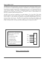
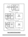
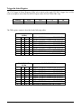
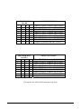
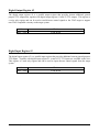
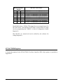
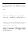
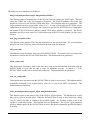
bus
CVXI-1149.1
VXIbus BOUNDARY SCAN
CONTROLLER BOARD
Copyright © 1992-1993, Corelis Inc.
USER'S MANUAL
P/N UM00090001-A2
Corelis Inc. 13100 Alondra Blvd. Suite 102, Cerritos, California 90703-2262
(310) 926-6727 • FAX (310) 404-6196
Table of Contents
PREFACE
Printing History.......................................................................................................................... i
Product Warranty ....................................................................................................................... ii
Exclusive Remedies ................................................................................................................... ii
CHAPTER 1 - PRODUCT OVERVIEW
About this Chapter ..................................................................................................................... 1-1
Introduction ................................................................................................................................ 1-2
What is IEEE 1149.1? ................................................................................................................ 1-3
Brief Product Review................................................................................................................. 1-4
Programmable Clock ................................................................................................................. 1-6
Parallel Input/Output Ports ........................................................................................................ 1-6
JTAG Compatible Logic ............................................................................................................ 1-7
Interrupts and Triggers............................................................................................................... 1-7
Front Panel ................................................................................................................................. 1-8
VXIbus A16 Registers ............................................................................................................... 1-8
VME/VXIbus Interface.............................................................................................................. 1-8
CVXI-1149.1 Specifications ...................................................................................................... 1-10
CHAPTER 2 - SYSTEM REQUIREMENTS
About this Chapter ..................................................................................................................... 2-1
Introduction ................................................................................................................................ 2-1
VXIbus Operation ...................................................................................................................... 2-2
Card Cages ................................................................................................................................. 2-3
Slot 0 Controller/Resource Manager ......................................................................................... 2-3
Host Computer ........................................................................................................................... 2-3
GPIB Host Interface................................................................................................................... 2-4
System Software ........................................................................................................................ 2-4
CHAPTER 3 - INSTALLATION AND CONFIGURATION
About this Chapter ..................................................................................................................... 3-1
Unpacking and Inspection ......................................................................................................... 3-1
Hardware Configuration ............................................................................................................ 3-3
VXIbus System Planning ........................................................................................................... 3-3
Configuration ............................................................................................................................. 3-5
Logical Address Selector ........................................................................................................... 3-5
VXIbus Chassis Slot .................................................................................................................. 3-5
CHAPTER 4 - HARDWARE DESCRIPTION
About this Chapter ..................................................................................................................... 4-1
Front Panel LEDs....................................................................................................................... 4-1
Front Panel Connectors .............................................................................................................. 4-2
A16 Registers ............................................................................................................................. 4-5
Absolute A16 Addressing .......................................................................................................... 4-6
ID Register ................................................................................................................................. 4-7
Table of Contents
Device Type Register................................................................................................................. 4-8
VXI Status Register ................................................................................................................... 4-8
Trigger-In Select Register .......................................................................................................... 4-9
Trigger-In Select Read-Back Register ....................................................................................... 4-11
Digital Output Register #1 ......................................................................................................... 4-11
Digital Input Register #1............................................................................................................ 4-11
Digital Output Register #2 ......................................................................................................... 4-12
Digital Input Register #2............................................................................................................ 4-12
Configuration Register #1 .......................................................................................................... 4-13
Configuration Register #2 .......................................................................................................... 4-15
SN74ACT8990 Registers........................................................................................................... 4-16
CHAPTER 5 - SOFTWARE DESCRIPTION
About this Chapter ..................................................................................................................... 5-1
Introduction ................................................................................................................................ 5-2
Selftest Software Source Code .................................................................................................. 5-5
APPENDIX A - SELFTEST SOFTWARE SOURCE CODE LISTINGS...................................... A-1
APPENDIX B - SN74ACT8990 APPLICAITON NOTE ................................................................. B-1
Table of Contents
PREFACE
Printing History
New editions are complete revisions of the manual. Update packages, which are issued between
editions, contain additional and replacement pages to be merged into the manual by the customer. The
dates on the title page change only when a new edition is published.
A software code may be printed before the date; this indicates the version of the software product at the
time the manual or update was issued. Many product updates and fixes do not require manual changes
and, conversely, manual corrections may be done without accompanying product changes. Therefore,
do not expect a one to one correspondence between product updates and manual updates.
Edition 1, October 1991
Edition 2, October 1992
Edition 3, November 1993
Edition 4, January 1994
Edition 5, October 1994
Edition 6, February 2011
Preface
i
Product Warranty
For product warranty and software maintenance information, see the PRODUCT WARRANTY AND
SOFTWARE MAINTENANCE POLICY statement included with your product shipment.
Exclusive Remedies
THE REMEDIES PROVIDED HEREIN ARE BUYER'S SOLE AND EXCLUSIVE REMEDIES.
CORELIS SHALL NOT BE LIABLE FOR ANY DIRECT, INDIRECT, SPECIAL, INCIDENTAL, OR
CONSEQUENTIAL DAMAGES, WHETHER BASED ON CONTRACT, TORT, OR ANY OTHER
LEGAL THEORY.
Product maintenance agreements and other customer assistance agreements are available for CORELIS
products. For assistance, contact your nearest CORELIS Sales and Service Office.
Return Policy
No items returned to CORELIS for warranty, service, or any other reason shall be accepted unless first
authorized by CORELIS, either direct or through its authorized sales representatives. All returned items
must be shipped pre-paid and clearly display a Returned Merchandise Authorization (RMA) number on the
shipping carton. Freight collect items will NOT be accepted. Customers or authorized sales representatives
must first contact CORELIS with notice of request for return of merchandise. RMA's can only originate
from CORELIS. If authorization is granted, an RMA number will be forwarded to the customer either
directly or through its authorized sales representative.
Contact Information
For sales inquiries, please contact [email protected].
For any support related questions, please enter a support request at www.corelis.com/support or email
[email protected].
For more information about other products and services that Corelis offers, please visit www.corelis.com.
Preface
ii
CHAPTER 1
PRODUCT OVERVIEW
About this Chapter
This chapter introduces you to the CVXI-1149.1 Boundary Scan Controller module. The main sections
of this manual are:
•
•
•
Note:
Introduction
What is IEEE-1149.1?
Brief Product Review
The CVXI-1149.1 is available as a "B" size module as well as a "C" size module. Unless
otherwise specified, this manual describes the features of both versions which are functionally
identical and differ by their physical dimensions only.
Product Overview
1-1
Introduction
The CVXI-1149.1 VXIbus Boundary Scan Controller Board provides an interface between the VXIbus
and any JTAG compatible target. The CVXI-1149.1 is designed to control the operation of an IEEE
standard 1149.1 (JTAG) test access port by generating the proper signals under software control to
interface with the target devices. Up to six test access ports can be controlled, each connecting the
CVXI-1149.1 card with a four signal cable to the boundary scanned target system. By controlling the
JTAG bus, boundary scan operations per IEEE-1149.1 can be invoked by software. The user is able to
command target circuitry Built-In-Self-Test (BIST), verify PCB interconnects, perform functional
testing, and debug without the need for manual probing. Furthermore, device internal functions that are
not accessible to external probing can be accessed through the JTAG interface, enabling fault isolation
within the device itself. A picture of the CVXI-1149.1 is shown in figure 1-1.
Figure 1-1 CVXI-1149.1 Module
Product Overview
1-2
What is IEEE 1149.1?
The IEEE 1149.1 test bus and boundary scan architecture allows an IC, and similarly a board or system,
to be controlled via a standard four-signal interface. Each IEEE 1149.1 compliant IC incorporates a
feature known as boundary scan that allows each functional pin of the IC to be controlled and observed
via the four-wire interface. Test, debug, or initialization patterns can be loaded serially into the
appropriate IC(s) via the IEEE 1149.1 test bus. This allows IC, board, or system functions to be
observed or controlled without actual physical access.
The IEEE 1149.1 test bus is comprised of two main elements: a Test Access Port (TAP), which
interfaces internal IC logic with the external world via a four-signal (optionally five-signal) bus as
shown in Figure 1-2; and a boundary scan architecture, which defines standard boundary cells to drive
and receive data at the IC pins. The IEEE 1149.1 specification also defines both mandatory and
optional opcodes and test features. The test bus signals are: Test Clock (TCK), Test Mode Select
(TMS), Test Data In (TDI), Test Data Out (TDO), and the optional Test Logic Reset (TRST).
The IEEE-1149.1 Test Access Port
Interface (TAP) consists of four
required signals:
Test Mode Select (TMS)
Test Clock (TCK)
Test Data In (TDI)
Test Data Out (TDO)
A fifth signal is defined as optional:
Test Reset (TRST*)
TMS
T
TCK
TDI
TDO
TRST*
A
P
Figure 1-2 Test Access Port (TAP)
Product Overview
1-3
Brief Product Review
The CVXI-1149.1 Boundary Scan Controller block diagram is shown in Figure 1-3. It is designed to
control the operation of an IEEE Standard 1149.1 (JTAG) scan test path by taking commands from the
host computer and generating the proper signals to interface with the target device(s). The host
computer can be an embedded VXIbus computer or an external host that controls the VXI chassis via a
VXIbus slot 0 controller. The target(s) can be moved from any stable state to another stable state,
loaded with instructions, and resulting test data scanned out to be read by the Host. Four EVENT pins
are provided to allow real-time interaction between the CVXI-1149.1 and its target(s). The EVENT
pins can be configured to generate VXIbus interrupt requests and/or assert TTL triggers whenever a
user-definable condition is present.
A 32-bit counter can be preset to allow a predetermined number of clock cycles or instruction
executions to occur and can be programmed to set an interrupt flag when it reaches a count of zero.
The CVXI-1149.1 implements all the low-level functions, enabling the host to use higher-level
abstraction such as states of IEEE Standard 1149.1 for control, variables indicating command finish,
buffer full or empty for status, and strings and buffers for data.
The CVXI-1149.1 may connect without external logic to six parallel chains of IEEE Standard 1149.1
targets, each with its own separate TMS signal. The parallel chains share one or two TDI signals, one
TDO signal, and one TRST signal and TCK signal.
The CVXI-1149.1 has four event detectors and two 16-bit event counters to support asynchronous
functions. The CVXI-1149.1 can connect to the target via a re-timed link with up to 31 bits of delay.
This may be required when the clock rate is high and either the target is at a distance or the link involves
fanout or buffer/driver devices.
The CVXI-1149.1 is an A16/D16 VXIbus slave device and interrupter with a 16-bit data bus. The
critical VXIbus interface timing is independent of the JTAG clock period.
The major functions of the CVXI-1149.1 are controlled by specific commands:
The STATE command controls the target interface and target state diagrams. It can change the current
state to any stable state.
The EXECUTE command causes the target to execute instructions that have been shifted into it. It uses
the Run-Test/ldle state, and can execute instructions for a fixed time or until an event occurs.
The SCAN command circulates data among targets and transfers data between the CVXI-1149.1 and
targets. It uses the Shift-IR or Shift-DR states, and also the read and write buffers.
Product Overview
1-4
Figure 1-3 CVXI-1149.1 Block Diagram
Product Overview
1-5
Programmable Clock
The CVXI-1149.1 card TCK clock output to the JTAG compatible target system is programmable by
user software. The user is able to select either an internal on-board XTAL oscillator or an external
target supplied clock.
The internal clock circuitry includes a programmable clock divider and pre-scaler logic. Any one of
sixteen different divide values, from divide by 2 to divide by 32, can be selected. A pre-scaler of divide
by 1 or divide by 32 can also be selected. Using the on-board 25 MHz crystal oscillator, 32 different
TCK rates ranging from 24.4 KHz to 12.5 MHz are user selectable.
If other clock rates are required, the user can select the external clock source and provide the clock
signal from either another VXIbus instrument or from the target system. Optionally, the user can install
his own crystal oscillator chip into the crystal oscillator socket that is provided on the CVXI-1149.1
card.
A single-step mode is also provided to enable the user to fully control the TCK signal high and low
states. When the single step mode is selected, the external clock source and the on-board crystal
oscillator are not used. Instead, the software write operations to the appropriate bit in the COMMAND
register toggle the TCK signal and result in a user controlled clock signal. The programmer is able to
single-step through the JTAG environment in a fully static mode of operation. This feature is very
useful for debugging software drivers and integrating complex JTAG compatible test systems.
Parallel Input/Output Ports
The board contains 32 TTL compatible parallel inputs and 32 TTL compatible parallel outputs. The
input and output signals are organized into 16 bit parallel ports. Each of the parallel input and output
ports are directly accessible by the host computer by reading or writing the appropriate VXIbus A16
register.
The 32 parallel outputs are driven by four tri-state octal buffers, with 8 outputs per buffer. The outputs
of each of the buffers can be put into tri-state under software control. The command register includes
four Output Enable bits, each of which controls one octal output buffer.
The input and output ports can be used to control and sense various non-JTAG functions in the target
system. These ports are useful for testing of target systems that incorporate a mixture of JTAG and nonJTAG compatible hardware.
Product Overview
1-6
JTAG Compatible Logic
The CVXI-1149.1 contains two JTAG compatible 74BCT8244 octal buffers that are connected in
parallel with the TTLTRG Trigger Input Select Register, which is one of the on-board A16 registers.
The serial test busses of the 74BCT8244 devices are daisy chained and then connected to the first set of
on-board serial test busses.
In normal mode of operation, these devices can be used as read-back buffers. Data written to the
Trigger-In select register port can be read-back from the particular A16 register assigned to these octal
buffers. In the diagnostic mode, the normal operation of the octal buffers is inhibited and the Test
Access Port circuitry is enabled to scan the device’s I/O boundary.
The user can program the Trigger-in Select register with arbitrary data, and then read it back via the
JTAG serial interface to verify that the data scanned matches the actual data presented at the buffer
input pins.
This feature provides extensive self-test capabilities on the CVXI-1149.1 board and enables the user to
exercise his software and test this "simple" JTAG compatible circuitry before attempting to connect to
more complicated target systems.
Interrupts and Triggers
The SN74ACT8990 test bus controller INTR interrupt request signal can be configured by the user to
drive one of the seven VXIbus interrupts and/or one of the eight VXIbus TTLTRG trigger lines. The
INTR signal is a programmable interrupt request that is set by external event signals and/or internal
SN74ACT8990 conditions. Refer to the SN74ACT8990 application note in Appendix B for additional
details regarding the operation of the INTR signal and the various programming options for this
powerful feature.
The use of interrupts and triggers is an important feature for synchronizing the target system with the
CVXI-1149.1 card and for synchronizing multiple VXI modules, including multiple CVXI-1149.1
cards. EVENT signals can detect an asynchronous event in the target system and consequently start or
stop serial JTAG data transmission or reception. External events can also be programmed to generate an
interrupt request to the host computer or trigger multiple VXIbus modules.
Product Overview
1-7
Front Panel
The front panel contains three LED indicators and two connectors. The front panel is shown in
Figure 1-4.
The RESET amber LED indicates that the JTAG TRST* signal is asserted.
The EXT CLK green LED indicates that an external JTAG clock source is being used.
The SLF TST green LED indicates that the target interface is in tri-state mode and that the on-board
loop-back option is selected (usually during self-test).
The TAP connector is a 40-pin 3M type connector that contains all the JTAG related interface signals.
The PIO connector is a 96-pin DIN connector that contains the 64 digital parallel I/O signals.
VXIbus A16 Registers
Thirty two 16-bit registers are provided which configure and control the operation of the CVXI-1149.1
card. The registers are located in the VXIbus A16 address space within a 40 hex address block that is
selected by the 8 bit logical address DIP switch. Chapter 4 provides a complete description of the
VXIbus A16 registers.
ADDRESS
OFFSET
$00
$02
$04
$06
$08
$0A
$0C
$0E
$10-$3E
REGISTER
READ/WRITE
VXI ID Register
VXI Device Type
VXI Status/Control
Trigger-In Select Register
Digital I/O Port #1
Digital I/O Port #2
Configuration Register #1
Configuration Register #2
SN74ACT8990 Registers
Read
Read
Read/Write
*Read/Write
Read/Write
Read/Write
Read/Write
Read/Write
Read/Write
* Note: Read-back register is implemented using two JTAG compatible 74BCT8244 devices.
VME/VXIbus Interface
The CVXI-1149.1 is an A16/D16 VME/VXIbus compatible slave module. The card is designed to
accept A16 mode address modifiers 29 hex and 2D hex. The card occupies 64 bytes (32 words) of
VXI/VME address space. The card address within the A16 address space is set by an 8 bit DIP switch
that selects one of 255 address blocks from $C000 to $FF80 in $40 (64 byte) increments.
All the on-board registers are 16 bits wide and are accessed via D16 data transfer cycles on the
VME/VXIbus.
Product Overview
1-8
IEEE-1149.1
CONTROLLER
RESET
EXT CLK
SLF TST
40
39
TAP
2
1
a b c
32
PIO
1
a b c
CVXI-1149.1
Figure 1-4 CVXI-1149.1 Front Panel
Product Overview
1-9
CVXI-1149.1 Specifications
VME/VXIbus Interface
Configurable Logical Addresses
I/O Width
I/O Space Size
Configurable IRQs
IEEE-1149.1
Number of TAP Controllers
Maximum TCK frequency
Maximum scanning data length
Parallel Ports
Output Voltage Compatibility
Output Current
Input Voltage Compatibility
Input Current
Physical
Board Outline Dimensions (PCB)
I/O Connectors
1 through 254
(default = 32)
D16 only
64 bytes (offsets $00 - $3F)
IRQ1 through IRQ7
(default = No IRQ connected)
6
12.5 MHz
232 bits
LS-TTL
24 ma (low), -2.6 ma (high)
LS-TTL
One LS-TTL load and 220/330Ω termination
to VCC/GND
C Size: 13.4" x 9.2" x 1.2"
B Size: 6.3" x 9.2" x 0.8"
1 JTAG Interface Connector
40-pin IDC [3M P/N 3432-5202 or equivalent]
1 Parallel I/O Connector
96-pin DIN [Harting P/N 09-03-196-6921 or equivalent]
Power Requirements
5 volts
2A maximum
Operating Environment
Temperature
Relative Humidity
Storage Environment
Temperature
Relative Humidity
Product Overview
0°C to 55°C
10% to 90%, non condensing
-40°C to 85°C
0% to 100%, non condensing
1-10
CHAPTER 2
SYSTEM REQUIREMENTS
About this Chapter
This chapter contains essential information regarding required hardware and software to operate the
CVXI-1149.1 Boundary Scan Controller Card. These requirements are described in the following
sections:
•
•
•
Introduction
VXIbus Operation
System Software
Introduction
To implement a VXIbus system, an appropriate VXIbus mainframe (or card cage) with which to
enclose, support inter-module triggering over the VXIbus, and provide necessary power is required.
The CVXI-1149.1 is designed to operate correctly when installed within any standard VXIbus card cage
systems that support C or B size modules.
To direct operation of installed VXIbus instruments, a host computer is required. This host can either be
located externally, or be embedded within the VXIbus enclosure system. However, which of the two
configurations is more advantageous depends on your system requirements. For example, an external
host may become necessary when use of a specific set of software tools are mandated. On the other
hand, if it is possible to use an embedded VXIbus-based computer, the simplification of the physical
design, improvement in throughput, and the potential for cost savings are important advantages to
consider.
System Requirements
2-1
VXIbus Operation
The CVXI-1149.1 is designed principally for VXIbus operation which provides for its highest level of
capability. When operated in that environment, a wide range of system configurations are supported
that can accommodate a broad class of applications, particularly those requiring many instruments. The
B size card, however, can be operated in any VMEbus compatible chassis. Although the VXIbus
specification imparts considerable architectural flexibility, for the purposes of this manual, only
'standard' approaches to operating the CVXI-1149.1 will be discussed. More elaborate configurations
(e.g. multiple host computers, etc.) are beyond the scope of this manual.
The basic elements required for an operational VXIbus system employing an external host computer are:
1 - VXIbus Card Cage
2 - VXIbus Slot 0 Controller/Resource Manager with GPIB Interface
3 - CVXI-1149.1 Module
4 - Other VXIbus Instrument Modules
5 - Host Computer with GPIB
6 - GPIB Cable
7 - Host GPIB Software Drivers
Note:
(A number of companies are offering alternative interfaces to the GPIB. This includes the
16-bit parallel MXI Interface, Ethernet, and others. For simplicity, only GPIB will be
referenced in this manual.)
Alternatively, the basic elements required for an operational VXIbus system employing an embedded
host computer are:
1- VXIbus Compatible Embedded Host Computer
(may or may not have built-in Slot 0 features)
2 - VXIbus Card Cage
3 - CVXI-1149.1 Module
4 - VXIbus Slot 0 Controller/Resource Manager
5 - Other VXIbus Instrument Modules
6 - Host-based VXIbus Instrument Software Drivers
System Requirements
2-2
Card Cages
The CVXI-1149.1 requires a card cage designed to VXIbus Specification Rev 1.2 or higher supporting
C-size modules. The B size version of the CVXI-1149.1 card will operate in any B-size VXIbus or
VMEbus compatible chassis. You can install as many CVXI-1149.1 modules into a single card cage as
is allowed electrically and physically. Power and available slots are often the main limiting factors.
The card requires a single +5V power supply with 2 amps maximum capability.
The card cage must provide forced-air cooling sufficient to maintain proper CVXI-1149.1 component
temperatures. It is suggested that the internal card cage air temperature not exceed 60 degrees
Centigrade with a minimum air velocity of 0.1 ft/sec at both sides of the module.
Slot 0 Controller/Resource Manager
To operate the CVXI-1149.1 in a VXIbus configuration, at least one Slot 0 Controller/Resource
Manager or its equivalent function must be present in the VXIbus chassis. This function, as described in
the VXIbus specification, manages hardware resources tied to the VXIbus and generally also provides a
GPIB interface to the host computer. Although they must all provide a minimum subset of functional
features as described in the VXIbus specification, these controllers are available in many forms, each
having specific key features. For example, some slot 0 controllers include the equivalent of an entire
host computer (see below) thereby making possible a stand-alone VXIbus based instrument system with
embedded controller in a single card cage.
As to the type of Slot 0 Controller/Resource Manager you choose for your system depends on the goals
and available hardware. The VXIbus standard is quite flexible with regard to topology and therefore
many paths may be possible for a given requirement. However, it is generally best to employ the least
complex approach where possible.
Host Computer
The CVXI-1149.1 requires a host computer to direct its operation. This host can either be embedded
into the VXIbus card cage or located externally and linked to the VXIbus card cage via GPIB. Any
computer having a GPIB port can potentially serve as an external host. Likewise, virtually any
VXIbus-based computer operating as a bus commander can function as a host. If the host computer is
embedded inside the VXIbus card cage, communication with the CVXI-1149.1 is register based.
Alternatively, if an embedded host has GPIB, it can link to the VXIbus slot 0 controller installed in the
same or other VXIbus card cage(s) over GPIB. This may be desirable in situations calling for a
consistent set of instrument drivers conversant with a single communication protocol such as GPIB.
Therefore when using an embedded controller to conserve space, the former requirement is satisfied by
employing its GPIB channel as the primary instrument control linkage, into and out of the VXIbus
environment. Figure 2-1 illustrates these basic configurations.
System Requirements
2-3
GPIB Host Interface
If the host is to reside external to the VXIbus system, a GPIB interface is required. Most computers that
have GPIB interfaces can be used to control the CVXI-1149.1 via VXIbus communication protocols.
To correctly operate the remote VXIbus system, appropriate GPIB commands must be issued. This is
generally accomplished using software drivers that are either supplied by the VXIbus Slot 0
manufacturer or user written.
System Software
In VXIbus external host computer configurations, host software drivers will be required to issue
appropriate GPIB commands, VXIbus Slot 0 Controller commands, and VXIbus Instrument commands.
Drivers for the GPIB and Slot 0 Controller/Resource Manager are usually supplied by the manufacturers
of the GPIB interface and Slot 0 Controller respectively. "C" source drivers are provided on a diskette
with each CVXI-1149.1 Module.
System Requirements
2-4
External Host Computer
with GPIB Interface card
Slot 0
CVXI
Controller 1149.1
with GPIB
OTHER
VXIbus
Instrument
modules
C-Size VXIbus Card Cage
GPIB/HP-IB
(a) External Host Configuration
Slot 0
Embed CVXI
Controller VXIbus 1149.1
with GPIB Comp
w GPIB
OTHER
VXIbus
Instrument
modules
Optional
GPIB
Equipment
C-Size VXIbus Card Cage
GPIB/HP-IB
(b) Embedded Host Linked to VXI with GPIB
Embedded
VXIbus
Computer
with Slot 0
& GPIB
CVXI
1149.1
OTHER VXIbus
Instrument
modules
Optional
GPIB
Equipment
C-Size VXIbus Card Cage
GPIB/HP-IB
(c) Embedded Host with VXI Slot 0 Function and GPIB
Figure 2-1 Example Host/VXI Linkage Configurations
System Requirements
2-5
CHAPTER 3
INSTALLATION AND CONFIGURATION
About this Chapter
This chapter contains important handling and VXIbus installation/configuration information for the
CVXI-1149.1 Boundary Scan Controller Card. Configuring the CVXI-1149.1 to operate in your
VXIbus system involves the setting of hardware switches which may have to be performed prior to
installation. This information is comprised of the following sections:
•
•
Unpacking and Inspection
Hardware Configuration
Unpacking and Inspection
To avoid possible damage and voiding of product warranty, it is imperative that the following handling
procedures be observed:
Unpacking
This product is packaged to protect it from possible causes of damage either by physical
means or by electrostatic discharge (ESD). It is important that an appropriate location be
used to perform unpacking. Such an area should be free of the possibility for ESD and
present no risk of physical damage.
IMPORTANT: If there is any sign of significant damage to the original shipping carton, report it
immediately to CORELIS and the shipping company.
Installation and Configuration
3-1
Once the original shipping carton has been opened and the individual items have been removed, place
them together for inspection. The CVXI-1149.1 hardware is packaged in anti-static protective material
and should be carefully removed to avoid destruction of this packing. Retain this along with the other
packing materials for possible future transport.
Inspection
The CVXI-1149.1 module should be free of any signs of physical damage. If this is not
the case, consult immediately with CORELIS or its authorized sales representative for
advisory information.
Installation and Configuration
3-2
Hardware Configuration
The VXIbus standard provides for modules of many purposes and manufacturers to reside in a single
VXIbus card cage. To operate together, all such modules in a VXIbus system must be properly
hardware configured. Therefore, before installing your CVXI-1149.1 module into the VXIbus system
card cage and applying power, it may have to be configured differently than the factory setting. Once
configured, these modules are then able to be managed by means of software commands via standard
VXIbus communication protocols.
NOTE: If you have already established how you are to configure the Logical Address of the
CVXI-1149.1, you can skip to the Logical Address Selector sub-section.
VXIbus System Planning
Due to the diversity of features found in VXIbus system elements, it is important to understand the
detailed requirements and capabilities of the specific modules you plan to install in your system and how
they are to interact. For example, not all Slot 0 Controller modules (or their equivalents) are created
equal. That is due to the fact that suppliers often differentiate their products by providing useful
proprietary high level features that assist VXIbus system implementation. As a result, such features can
have great influence on the topological approach selected during VXIbus system design.
An important step in the design process is the planning of the VXIbus system structure by establishing
module hierarchy such as commander-servant relationships. This is best done by charting out the full
list of instruments and required control modules based on available features and your system
requirements. Figure 3-1 provides an example chart that can be used for this purpose. However, details
of how to best configure your system are beyond the scope of this manual.
Although the VXIbus specification contains fundamental information in this regard, more practical
knowledge can be obtained from user's manuals of VXIbus modules, particularly those of VXIbus
controllers. The reason for this is that controller products embody many of the primary system features
that most influence configuration possibilities.
Installation and Configuration
3-3
SLOT
NUMBER
LOGICAL
ADDRESS
SECONDARY
HPIB
ADDRESS
MODULE
Figure 3-1 Example VXIbus System Configuration Chart
Installation and Configuration
3-4
Configuration
The CVXI-1149.1 module possesses a Logical Address DIP switch with which to manually determine
specific address configurations from 0 to 255. A setting of 0 is reserved for slot 0 controller modules,
and the value 255 is reserved to signal that the VXIbus resource manager is to perform dynamic logical
address configuration on the instrument. The CVXI-1149.1 does not support dynamic logical address
configuration.
The instrument must be set to an address between 1 and 254, so the module is, in VXI terminology,
configured statically.
NOTE: No two modules should have the same Logical Address in any group of VXIbus modules being
controlled by the same slot 0/resource manager
Logical Address Selector
Once your VXIbus system hierarchical structure has been determined, the next step is to configure the
CVXI-1149.1 logical address to the chosen value. The factory default is set to 32. If you wish to
change this, the proper position for each of the 8 switches yielding the desired value must be
determined.
NOTE: As shown in Figure 3-2 the Logical Address DIP Switch, accessed through the module cover,
forms its value based on the sum of the decimal values of the switches in the OPEN (1)
position. Examples of this are shown in this figure.
VXIbus Chassis Slot
The CVXI-1149.1 can be installed into any available VXIbus backplane slot except slot 0.
Installation and Configuration
3-5
128 64 32 16 8 4 2 1
1
NOTE:
2
3
4
5
6
7
8
0
Switches shown in
Factory Default
Positions
1
OPEN
7 6 5 4 3 2 1 0
Logical Address Selector
Setting Logical Address:
A
The Logical Address is the sum of
Switch set to '0'
B
Switch set to '1'
C the decimal values of the switches
depressed in the '1' (open) position
Figure 3-2 Logical Address Selector DIP Switch
Installation and Configuration
3-6
CHAPTER 4
HARDWARE DESCRIPTION
About this Chapter
This chapter contains information regarding the description of the CVXI-1149.1 hardware.
information is contained in the following sections:
•
•
•
•
•
•
•
•
•
•
•
•
•
•
•
This
Front Panel LED's
Front Panel Connectors
A16 Registers
ID Register
Device Type Register
VXI Status Register
Trigger-in Select Register
TSR Read-Back Register
Digital Output Register #1
Digital Input Register #1
Digital Output Register #2
Digital Input Register #2
Configuration Register #1
Configuration Register #2
TBC Chip Registers
Front Panel LEDs
The three CVXI-1149.1 card front panel LED's are described in table 4-1. The LED's are directly
controlled by the appropriate bits in Configuration Register #1:
LED
RESET
COLOR
Amber
EXT CLK
Green
SLF TST
Green
DESCRIPTION
Illuminates when the TRGRST* bit (D6) of Control Register #1
is asserted (low).
Illuminates when the CLKSEL1 bit (D12) of Control Register #1
is set to "1" (high).
Illuminates when the TRGOFF* bit (D5) of Control Register #1
is asserted (low).
Table 4-1 Front Panel LED Description
Hardware Description
4-1
Front Panel Connectors
JTAG Connector
The JTAG interface connector (labeled TAP) is a 40-pin 3M type connector that includes all the
signals for the six serial boundary scan access ports. This connector is located on the upper
portion of the front panel of the card. The pinout of the TAP connector is shown in table 4-2.
PIN
1
3
5
7
9
11
13
15
17
19
21
23
25
27
29
31
33
35
37
38
39
40
SIGNAL NAME
TRST*
TDO
TDI0
TMS0
TCK
T OFF*
SENSE*
TCKI
TDI1
TMS1
EVENT0
EVENT1
EVENT2
EVENT3
TEST TDI
TEST TDO
TEST TMS
TEST TCK
TMS2
TMS4
TMS3
TMS5
I/O
Out
Out
In
Out
Out
In
In
In
In
Out
In
In
In
In
In
Out
In
In
Out
Out
Out
Out
DESCRIPTION
Target reset command signal
Test Data Output
Test Data Input - Channel 0
Test Mode Select - Channel 0
Test Serial Clock
"Target power off" indicator (active low)
"Target cable connected" sense line
External clock signal from the target
Test Data Input - Channel 1
Test Mode Select - Channel 1
SN74ACT8990 EVENT0 signal
SN74ACT8990 EVENT1 signal
SN74ACT8990 EVENT2 signal
SN74ACT8990 EVENT3 signal
TDI of the on-board test circuit (BCT8244's)
TDO of the on-board test circuit (BCT8244's)
TMS of the on-board test circuit (BCT8244's)
TCK of the on-board test circuit (BCT8244's)
Test Mode Select - Channel 2
Test Mode Select - Channel 4
Test Mode Select - Channel 3
Test Mode Select - Channel 5
All other pins of the connector (2,4,6,8...,36) are connected to ground (GND).
Table 4-2 JTAG Interface Pinout
Hardware Description
4-2
PIO Connector
The PIO connector is a standard Eurocard 96-pin male DIN connector. This connector can be used to
interface non-JTAG circuitry to the CVXI-1149.1 parallel I/O ports in order to support testing of target
systems that incorporate both JTAG and non-JTAG circuitry. There are 32 parallel inputs and 32
parallel outputs that connect to rows A and C of the 3 row 96-pin DIN connector. Row B is connected
to ground. The pin-out of the PIO connector is shown in tables 4-3 and 4-4.
DIGITAL I/O
Digital Input Register #1
Digital Input Register #1
Digital Input Register #1
Digital Input Register #1
Digital Input Register #1
Digital Input Register #1
Digital Input Register #1
Digital Input Register #1
Digital Input Register #1
Digital Input Register #1
Digital Input Register #1
Digital Input Register #1
Digital Input Register #1
Digital Input Register #1
Digital Input Register #1
Digital Input Register #1
Digital Output Register #1
Digital Output Register #1
Digital Output Register #1
Digital Output Register #1
Digital Output Register #1
Digital Output Register #1
Digital Output Register #1
Digital Output Register #1
Digital Output Register #1
Digital Output Register #1
Digital Output Register #1
Digital Output Register #1
Digital Output Register #1
Digital Output Register #1
Digital Output Register #1
Digital Output Register #1
BIT
PIO CONNECTOR PIN
0 (LSB)
A1
1
A2
2
A3
3
A4
4
A5
5
A6
6
A7
7
A8
8
A9
9
A10
10
A11
11
A12
12
A13
13
A14
14
A15
15 (MSB)
A16
0 (LSB)
A17
1
A18
2
A19
3
A20
4
A21
5
A22
6
A23
7
A24
8
A25
9
A26
10
A27
11
A28
12
A29
13
A30
14
A31
15 (MSB)
A32
Table 4-3 PIO Connector Row A Pinout
Hardware Description
4-3
DIGITAL I/O
Digital Input Register #2
Digital Input Register #2
Digital Input Register #2
Digital Input Register #2
Digital Input Register #2
Digital Input Register #2
Digital Input Register #2
Digital Input Register #2
Digital Input Register #2
Digital Input Register #2
Digital Input Register #2
Digital Input Register #2
Digital Input Register #2
Digital Input Register #2
Digital Input Register #2
Digital Input Register #2
Digital Output Register #2
Digital Output Register #2
Digital Output Register #2
Digital Output Register #2
Digital Output Register #2
Digital Output Register #2
Digital Output Register #2
Digital Output Register #2
Digital Output Register #2
Digital Output Register #2
Digital Output Register #2
Digital Output Register #2
Digital Output Register #2
Digital Output Register #2
Digital Output Register #2
Digital Output Register #2
BIT
PIO CONNECTOR PIN
0 (LSB)
C1
1
C2
2
C3
3
C4
4
C5
5
C6
6
C7
7
C8
8
C9
9
C10
10
C11
11
C12
12
C13
13
C14
14
C15
15 (MSB)
C16
0 (LSB)
C17
1
C18
2
C19
3
C20
4
C21
5
C22
6
C23
7
C24
8
C25
9
C26
10
C27
11
C28
12
C29
13
C30
14
C31
15 (MSB)
C32
Table 4-4 PIO Connector Row C Pinout
Hardware Description
4-4
A16 Registers
Table 4-5 lists all the A16 registers on the CVXI-1149.1 module. The registers are shown sorted by
their address offset from the base address of the module.
Address
Offset
$00
$02
$04
$06
$06
$08
$08
$0A
$0A
$0C
$0E
$10
$12
$14
$16
$18
$1A
$1C
$1E
$20
$22
$24
$26
$28
$2A
$2C
$2E
$30
$32
$34
$36
$38
$3A
$3C
$3E
A16 Register
Accessibility
VXI ID Register (always reads $FF00)
VXI Device Type Register (always reads $047D)
VXI Status Register
VXI Trigger-In Select Register (TSR)
TSR Read-Back Register (Two 74BCT8244 JTAG IC's)
Digital Output Register #1
Digital Input Register #1
Digital Output Register #2
Digital Input Register #2
Configuration Register #1
Configuration Register #2
TBC Control0 Register
TBC Control1 Register
TBC Control2 Register
TBC Control3 Register
TBC Control4 Register
TBC Control5 Register
TBC Control6 Register
TBC Control7 Register
TBC Control8 Register
TBC Control9 Register
TBC Minor Command Register
TBC Major Command Register
TBC Counter1 Update0 Register
TBC Counter1 Update1 Register
TBC Counter2 Update0 Register
TBC Counter2 Update1 Register
TBC Status0 Register
TBC Status1 Register
TBC Status2 Register
TBC Status3 Register
TBC Capture0 Register
TBC Capture1 Register
TBC Read Buffer Register
TBC Write Buffer Register
Read
Read
Read
Write
Read
Write
Read
Write
Read
Read/Write
Read/Write
Read/Write
Read/Write
Read/Write
Read/Write
Read/Write
Read/Write
Read/Write
Read/Write
Read/Write
Read/Write
Read/Write
Read/Write
Read/Write
Read/Write
Read/Write
Read/Write
Read
Read
Read
Read
Read
Read
Read
Write
Table 4-5 CVXI-1149.1 A16 Registers
Hardware Description
4-5
Absolute A16 Addressing
Some software requires the user to specify the absolute A16 address of a register to be accessed. The
base address of the CVXI-1149.1 can be calculated by using the following formula:
$C000 + (Logical_Address * $40)
or (decimal)
49,152 + (Logical_Address * 64)
The address $C000 is defined by VXIbus as the beginning of A16 space which is dedicated to each
module installed in a system. Each logical address in a VXIbus system is dedicated 64 bytes of the
upper 16Kb of A16 space.
The factory set logical address is 32 which yields a base address of:
$C000 + (32 * $40)
$C000 + $0800 = $C800
or (decimal)
49,152 + (32 * 64)
49,152 + 2048 = 51,200
To access registers on the card, the offset of the register is added to the base address of the card to form
a complete A16 address. For example, configuration register #1 has an offset of $0C. Adding this
offset to the base address of $C800 (assuming the default logical address 32) yields an A16 address of
$C80C.
Hardware Description
4-6
ID Register
The CVXI-1149.1 ID Register indicates the classification, addressing mode, and the manufacturer of the
device.
Address
Base + $00
15 - 14
Device
Class
13 - 12
Address
Mode
11 - 0
Manufacturer ID
Device Classification: Bits 15 and 14 classify a device as one of the following:
0 0 memory device
1 0 extended device
1 0 message-based device
1 1 register based device
The CVXI-1149.1 module is a register based device.
Addressing Mode: Bits 13 and 12 indicate the addressing mode used by the device:
0 0 A16/A24 address mode
0 1 A16/A32 address mode
1 0 RESERVED
1 1 A16 address mode only
The CVXI-1149.1 module uses the A16 address mode only.
Manufacturer ID: Bits 11 through 0 identify the manufacturer of the device. The Corelis ID number
is 3840 which corresponds to bits 11-0 being set to $0F00.
Given the device classification, addressing space, and manufacturer of the CVXI-1149.1 module,
reading the ID register will always return the value $FF00.
Hardware Description
4-7
Device Type Register
The Device Type register contains a model code which identifies the device.
Address
Base + $02
15 - 12
Required
Memory
11-0
Model Code
Required Memory: Since the CVXI-1149.1 is an A16 only device, this field will always be zero.
Model Code: The model code which identifies the CVXI-1149.1 module is $047D (1149 decimal).
VXI Status Register
The VXI status register contains status bits for various functions of the CVXI-1149.1 card. The register
content is described in the following table:
Address
Base +
$04
15
14
13
12
0 MODID* 0 RDY*
11
INT*
10
SENSE*
9
TOFF
8-4
0
3
1
2
1
1
0
0
0
MODID* This bit indicates the status of the VXIbus MODID signal. The slot 0 controller uses this
active low bit to select cards in the VXIbus chassis.
RDY*
This active low bit reflects the state of the SN74ACT8990 (TBC) RDY signal. When
asserted, it indicates that the TBC is ready for additional commands and/or data.
INT*
This active low bit reflects the state of the SN74ACT8990 (TBC) INT signal. When
asserted, it indicates that the TBC is sending an interrupt to the host.
SENSE*
This bit, when low, indicates that the SENSE signal on the JTAG interface connector is
connected to GND. This signal can be used by the software to sense that an external cable
is connected to the card JTAG connector.
TOFF
This bit, when high, indicates that the target power is off at the JTAG interface connector.
Hardware Description
4-8
Trigger-In Select Register
The VXI Trigger-in Select Register (TSR) selects which of the eight TTLTRG* trigger lines will be
used as an input to each of the four EVENT inputs of the SN74ACT8990 TBC chip.
Address
Base + $06
15-12
Event 3 Select
11-8
Event 2 Select
7-4
Event 1 Select
3-0
Event 0 Select
The TSR register content is described in the following tables:
REGISTER BITS
D3-D0
1
0
0
0
1
0
0
1
1
0
1
0
1
0
1
1
1
1
0
0
1
1
0
1
1
1
1
0
1
1
1
1
0
X
X
X
REGISTER BITS
D7-D4
1
0
0
0
1
0
0
1
1
0
1
0
1
0
1
1
1
1
0
0
1
1
0
1
1
1
1
0
1
1
1
1
0
X
X
X
Hardware Description
SELECT FUNCTION
VXIbus TTLTRG0* is input to TBC EVENT0
VXIbus TTLTRG1* is input to TBC EVENT0
VXIbus TTLTRG2* is input to TBC EVENT0
VXIbus TTLTRG3* is input to TBC EVENT0
VXIbus TTLTRG4* is input to TBC EVENT0
VXIbus TTLTRG5* is input to TBC EVENT0
VXIbus TTLTRG6* is input to TBC EVENT0
VXIbus TTLTRG7* is input to TBC EVENT0
No signal is connected to the TBC EVENT0
SELECT FUNCTION
VXIbus TTLTRG0* is input to TBC EVENT1
VXIbus TTLTRG1* is input to TBC EVENT1
VXIbus TTLTRG2* is input to TBC EVENT1
VXIbus TTLTRG3* is input to TBC EVENT1
VXIbus TTLTRG4* is input to TBC EVENT1
VXIbus TTLTRG5* is input to TBC EVENT1
VXIbus TTLTRG6* is input to TBC EVENT1
VXIbus TTLTRG7* is input to TBC EVENT1
No signal is connected to the TBC EVENT1
4-9
REGISTER BITS
D11-D8
1
0
0
0
1
0
0
1
1
0
1
0
1
0
1
1
1
1
0
0
1
1
0
1
1
1
1
0
1
1
1
1
0
X
X
X
REGISTER BITS
D15-D12
1
0
0
0
1
0
0
1
1
0
1
0
1
0
1
1
1
1
0
0
1
1
0
1
1
1
1
0
1
1
1
1
0
X
X
X
SELECT FUNCTION
VXIbus TTLTRG0* is input to TBC EVENT2
VXIbus TTLTRG1* is input to TBC EVENT2
VXIbus TTLTRG2* is input to TBC EVENT2
VXIbus TTLTRG3* is input to TBC EVENT2
VXIbus TTLTRG4* is input to TBC EVENT2
VXIbus TTLTRG5* is input to TBC EVENT2
VXIbus TTLTRG6* is input to TBC EVENT2
VXIbus TTLTRG7* is input to TBC EVENT2
No signal is connected to the TBC EVENT2
SELECT FUNCTION
VXIbus TTLTRG0* is input to TBC EVENT3
VXIbus TTLTRG1* is input to TBC EVENT3
VXIbus TTLTRG2* is input to TBC EVENT3
VXIbus TTLTRG3* is input to TBC EVENT3
VXIbus TTLTRG4* is input to TBC EVENT3
VXIbus TTLTRG5* is input to TBC EVENT3
VXIbus TTLTRG6* is input to TBC EVENT3
VXIbus TTLTRG7* is input to TBC EVENT3
No signal is connected to the TBC EVENT3
This register bits will be all 0's upon power-up reset.
Hardware Description
4-10
Trigger-In Select Read-Back Register
The Trigger-In Select Read-Back register is a 16-bit wide buffer that enables the user to read back data
from the Trigger-in Select Register (TSR). The TSR Read-Back register is implemented using two
74BCT8244 buffer IC's that are also IEEE-1149.1 (JTAG) compatible.
When the target JTAG interface is turned off (see Configuration Register #1 description), the two
74BCT8244 devices are automatically connected to the first of the six on-board JTAG channels
(channel 0). The operation of the JTAG Test Access Port (TAP) can now be verified using this "simple"
on-board JTAG circuitry. First, the software writes arbitrary data to the TSR, then it reads the TSR
Read-Back register and verifies that the appropriate data is received. The data can be read from the TSR
Read-Back register either directly, or via the JTAG interface.
Address
Base + $06
15 - 0
16 Bit Word
Digital Output Register #1
The digital output register #1 is a parallel output register that provides up to sixteen general purpose
TTL outputs. This register is a write only register and can be used to send discrete control signals to the
JTAG target to support non-JTAG compatible circuitry on the target system.
Address
Base + $08
15 - 0
16 Bit Word
Digital Input Register #1
The digital input register #1 is a parallel input register that provides up to sixteen general purpose TTL
inputs. This register is a read only register and can be used to input discrete control signals from the
target system.
Address
Base + $08
Hardware Description
15 - 0
16 Bit Word
4-11
Digital Output Register #2
The digital output register #2 is a parallel output register that provides sixteen additional general
purpose TTL outputs that, together with digital output register #1 total 32 TTL outputs. This register is
a write only register and can be used to send discrete control signals to the JTAG target to support
non-JTAG compatible circuitry on the target system.
Address
Base + $0A
15 - 0
16 Bit Word
Digital Input Register #2
The digital input register #2 is a parallel input register that provides additional sixteen general purpose
TTL inputs. Together with digital input register #1, a total of 32 TTL inputs are available to the user.
This register is a read only register and can be used to input discrete control signals from the target
system.
Address
Base + $0A
Hardware Description
15 - 0
16 Bit Word
4-12
Configuration Register #1
Configuration register #1 is a read/write register that determines certain modes of operation for the
JTAG interface logic. These register bits will be all 0's upon power-up reset. The register is described
in the following table:
Address
Base + $0C
15
Unused
14
FREE_RUN
13
Unused
12
CLKSEL1
11 - 8
BYTEN
Address
Base + $0C
7
STEP*
6
TRGRST*
5
TRGOFF*
4
CLKSEL0
3-0
DIV
DIV3-0
These 4 bits determine the divider used to generate the JTAG interface TCK serial shift
clock as per the following table:
DIV 3 DIV 2
0
0
0
0
0
0
0
0
0
1
0
1
0
1
0
1
1
0
1
0
1
0
1
0
1
1
1
1
1
1
1
1
DIV 1
0
0
1
1
0
0
1
1
0
0
1
1
0
0
1
1
DIV 0
0
1
0
1
0
1
0
1
0
1
0
1
0
1
0
1
DIVIDER
Divide by 2
Divide by 4
Divide by 6
Divide by 8
Divide by 10
Divide by 12
Divide by 14
Divide by 16
Divide by 18
Divide by 20
Divide by 22
Divide by 24
Divide by 26
Divide by 28
Divide by 30
Divide by 32
CLKSEL 1-0 Select the clock source for the JTAG interface. Once the clock source is selected, it will
be divided by the prescaler pointed by the DIV3-0 bits and then used by the JTAG
circuitry. The CLKSEL bits function as shown in the following table:
CLKSEL1
0
0
1
1
Hardware Description
CLKSEL0
0
1
0
1
CLOCK SOURCE
Internal clock - 25 MHz
Internal clock - 781 KHz
VXIbus TTLTRG signal
External clock (JTAG Connector)
4-13
TRGOFF*
This active low signal causes the JTAG interface to the target system to go tri-state and
electrically disconnect itself from the target.
When the TRGOFF* signal is low, the two on-board JTAG compatible 74BCT8244
devices are connected in series with the channel 0 signals of the SN74ACT8990 TBC
chip. This enable self-test and diagnostics software to fully test the functionality of the
JTAG interface prior to attaching it to the target system.
TRGRST*
This active low signal directly drives the on-board SN74ACT8990 TBC chip reset input
pin. It also drives the TRST* signal on the front panel JTAG connector.
The TRST* signal is defined in the IEEE-1149.1 specification as an optional Test Access
Port signal. It can be used to reset the target JTAG interface and circuitry.
STEP*
An active low single-step control signal that enables the software to directly drive the
JTAG clock signal and be able to single step the interface logic under software control.
When asserted, the TCK signal is driven directly by the DIV0 bit of this register.
BYTEN
These four bits control the enabling of the 32 parallel outputs. The description of each
bit is given in the following table:
Bit
8
Mnemonic
BYTEN1
9
BYTEN2
10
BYTEN3
11
BYTEN4
Description
An active high byte-enable signal for the discrete output register.
When this bit is asserted, the least significant eight bits of Output
Register #1 are enabled.
An active high byte-enable signal for the discrete output register.
When this bit is asserted, the most significant eight bits of
Output Register #1 are enabled.
An active high byte-enable signal for the discrete output register.
When this bit is asserted, the least significant eight bits of Output
Register #2 are enabled.
An active high byte-enable signal for the discrete output register.
When this bit is asserted, the most significant eight bits of
Output Register #2 are enabled.
FREE_RUN This bit, when set, indicates that the TCK output (pin 9) on the TAP Connector will freerun. Otherwise, the TCK output will be controlled by the 74ACT8990 (TCKO).
Hardware Description
4-14
Configuration Register #2
Configuration register #2 is a read/write register that selects VXIbus interrupts and triggers to/from the
SN74ACT8990 (TBC) chip. This register will be set to 0 upon power-up reset.
Address
Base + $0E
15 - 11
not used
10 - 8
EXTCLK
7-4
TTLTRG*
Select
3-0
VXI INTR*
Select
The register is described in the following table:
REGISTER BITS
D3-D0
1
0
0
0
1
0
0
1
1
0
1
0
1
0
1
1
1
1
0
0
1
1
0
1
1
1
1
0
1
1
1
1
0
X
X
X
SELECT FUNCTION
No VXIbus interrupt is active
TBC INT-is connected to VXIbus IRQ1*
TBC INT-is connected to VXIbus IRQ2*
TBC INT-is connected to VXIbus IRQ3*
TBC INT-is connected to VXIbus IRQ4*
TBC INT-is connected to VXIbus IRQ5*
TBC INT-is connected to VXIbus IRQ6*
TBC INT-is connected to VXIbus IRQ7*
No signal is connected to the VXIbus interrupt lines
Bits D3 - D0 select which VXIbus interrupt line the SN74ACT8990 interrupt will
be connected to.
REGISTER BITS
D7-D4
1
0
0
0
1
0
0
1
1
0
1
0
1
0
1
1
1
1
0
0
1
1
0
1
1
1
1
0
1
1
1
1
0
X
X
X
SELECT FUNCTION
TBC INT is connected to VXIbus TTLTRG0*
TBC INT is connected to VXIbus TTLTRG1*
TBC INT is connected to VXIbus TTLTRG2*
TBC INT is connected to VXIbus TTLTRG3*
TBC INT is connected to VXIbus TTLTRG4*
TBC INT is connected to VXIbus TTLTRG5*
TBC INT is connected to VXIbus TTLTRG6*
TBC INT is connected to VXIbus TTLTRG7*
No signal is connected to the VXIbus trigger lines
Bits D7 - D4 select which VXIbus TTL trigger line the SN74ACT8990 interrupt
will be connected to.
Hardware Description
4-15
REGISTER BITS
D10-D8
0
0
0
0
0
1
0
1
0
0
1
1
1
0
0
1
0
1
1
1
0
1
1
1
SELECT FUNCTION
TTLTRG0* is connected to JTAG clock mux
TTLTRG1* is connected to JTAG clock mux
TTLTRG2* is connected to JTAG clock mux
TTLTRG3* is connected to JTAG clock mux
TTLTRG4* is connected to JTAG clock mux
TTLTRG5* is connected to JTAG clock mux
TTLTRG6* is connected to JTAG clock mux
TTLTRG7* is connected to JTAG clock mux
Bits D10-D8 select a VXIbus TTL trigger line as an external source for
the JTAG clock. Note that the JTAG clock is selected from a 4 input
mux by programming the CLKSEL 1,0 bits in Configuration Control
Register #1.
Bits D15-D11 are unused and can be utilized by the software for
testing/diagnostics.
SN74ACT8990 Registers
A detailed description of the SN74ACT8990 Test Bus Controller (TBC) chip registers is provided in
Appendix B.
Hardware Description
4-16
CHAPTER 5
SOFTWARE DESCRIPTION
About this Chapter
This chapter describes the "C" source coded self-test software and drivers that are provided with each
CVXI-1149.1 module. This is comprised of the following sections:
•
•
•
•
•
•
•
•
•
•
•
•
•
•
•
Introduction
Hardware Configuration
scan_ir() routine
scan_dr() routine
circulate_dr() routine
hard_reset() routine
wait_jtag_state() routine
soft_reset() routine
check_ready() routine
wait_for_ready() routine
write_tbc() routine
read_tbc() routine
write_buf() routine
read_buf() routine
Selftest Software Listings
Software Description
5-1
Introduction
The sample "C" code diskette provided with the CVXI-1149.1 card is intended to serve two functions.
First, this code is the actual C language source code for the executable selftest program included on the
disk. Second, this code provides functions which will be useful either directly or as example code to a
programmer writing software to operate the CVXI-1149.1. Three different versions of the software are
supplied to support various hosts. All source code was compiled with the Borland C compiler.
The functions provided in the source code can be classified in two categories:
Scanning
Utility/Low-level access
The Scanning functions provide a higher level access to the operation of the SN74ACT8990 IC. These
functions are:
scan_ir(unsigned short *output, unsigned short length, unsigned short *input)
This function scans an arbitrary length bit stream into the TAP controller instruction register. This
function takes three parameters. The output parameter is an address to an array of 16-bit values to be
scanned out the JTAG instruction path. The length parameter specifies the length of the bit stream
(pointed to by output). The input parameter specifies the address of 16-bit values where the data
scanned in is to be stored.
scan_dr(unsigned short *output, unsigned short length, unsigned short *input)
This function scans an arbitrary length bit stream through the TAP controller data path. This function
takes three parameters. The output parameter is an address to an array of 16-bit values to be scanned
out the JTAG data path. The length parameter specifies the length of the bit stream (pointed to by
output). The input parameter specifies the address of 16-bit values where the data scanned in is to be
stored.
circulate_dr(unsigned short length, unsigned short *data)
This function circulates an arbitrary length bit stream through the TAP controller data path. This is
accomplished by initially shifting dummy data through the TAP data path to get valid data out, and
then reshifting the valid data back into the path. This allows a data path to be inspected without
modifying its contents. This function takes two parameters. The length parameter specifies the
length of the bit stream to be circulated. The data parameter specifies the address of 16-bit values
where the data scanned in is to be stored.
Software Description
5-2
The utility/low-level functions are as follows:
hard_reset(unsigned short target, unsigned short divider)
This function causes a hardware reset of the SN74ACT8990 by pulsing its *TRST input. This also
causes the *TRST line of the JTAG targets to be pulsed. The result of hardware reset on the chip
should be reviewed in the SN74ACT8990 data sheet. This function takes two parameters. The
target parameter can have two possible values, 0 or 1. A value of 0 specifies the ACT8990 is to be
connected to the external JTAG targets, and a value of 1 specifies the ACT8990 is to be connected to
the internal JTAG 8244 devices, and the external JTAG target interface is tri-stated. The divider
parameter specifies a value from 0 to 15 which selects on of the TCK clock dividers (see the control
register).
wait_jtag_state(short state)
This function waits until the JTAG bus has transitioned to the specified state. The state parameter
specifies one of the JTAG bus states as defined at the start of the test program.
soft_reset(void)
This function causes a software only reset of the SN74ACT8990. The result of soft reset on the chip
should be reviewed in the SN74ACT8990 data sheet. This function takes no parameters.
check_ready(void)
The check ready function is used by the low level read and write functions associated with the
SN74ACT8990 to verify that the chip is ready for additional accesses. It returns a 1 if the
SN74ACT8990 is ready to be accessed, and 0 otherwise. This function takes no parameters.
wait_for_ready(void)
This function does not return until the SN74ACT8990 is ready to be accessed. This implemented by
continually polling the status register until a value of 0 is read in the RDY* bit position. This
function takes no parameters.
write_tbc(unsigned short register_offset, unsigned short data)
This function writes a data value to one of the SN74ACT8990 registers. The function first verifies
that register_offset is a valid offset. When the SN74ACT8990 is ready to be accessed (by calling
wait_for_ready()) the data is written to the specified register. No checking is done to see if the
register is a read only register. This function takes two parameters. The register_offset parameter
specifies which register on the SN74ACT8990 to write, and the data parameter specifies the data to
be written.
Software Description
5-3
read_tbc(unsigned short register_offset, unsigned short *data)
This function reads a data value from one of the SN74ACT8990 registers. The function first verifies
that register_offset is a valid offset. When the SN74ACT8990 is ready to be accessed (by calling
wait_for_ready()) the data is read from the specified register and stored at the specified location. No
checking is done to see if the register is a write only register. This function takes two parameters.
The register_offset parameter specifies which register on the SN74ACT8990 to read, and the data
parameter specifies the address where the read data is to be stored.
write_buf(unsigned short data)
This function writes a data value to the SN74ACT8990 output shift register. It polls the
SN74ACT8990 STATUS2 register until the write_OK flag indicates data may be written to the shift
register buffer, at which time the specified data is written out. This function takes one parameter
data which is the data to be stored in the output shift register.
read_buf(unsigned short *data)
This function reads a data value from the SN74ACT8990 input shift register. It polls the
SN74ACT8990 STATUS2 register until the read_OK flag indicates data is available to be read, at
which time the input shift register buffer is read. This function takes one parameter data which
specifies the address where the read data is to be stored.
Software Description
5-4
Selftest Software Source Code
C language source code is provided for the selftest software. Several different versions of the software
are supplied for various interfaces. Check the CVXI-1149.1 selftest software and driver disk for
available source code. Currently, the supported interfaces are as follows:
1. RadiSys EPC-2/2e 80386 or EPC-7 80486 Embedded PC.
2. National Instruments MXI interface.
3. National Instruments LabWindows.
4. Hewlett-Packard's E1405A slot-0 controller using an HP IEEE-488 controller card installed in a PC.
Software Description
5-5
APPENDIX A
SELFTEST SOFTWARE SOURCE CODE LISTINGS
Refer to the CVXI-1149.1 Self-Test Software and Driver Disk.
Selftest Software Source Code Listings
A-1
APPENDIX B
SN74ACT8990 APPLICATION NOTE
The following pages contain the SN74ACT8990 application note.
SN74ACT8990 Application Note
B-1