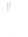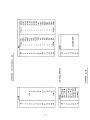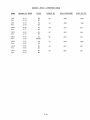
1
NATIONAL RADIO ASTRONOMY OBSERVATORY CHARLOTTESVILLE, VIRGINIA ELECTRONICS DIVISION INTERNAL REPORT No. 187 THE NRAO VLBI MARK II PROCESSOR B. MEREDITH AND B. RAYHRER JUNE 1978 NUMBER OF COPIES: 150 INDEX PAGE CHAPTER 1: Introduction Photograph of the Processor ............... Block Diagram of Control CPU and FFT Processor ....................................... Specification of Buffer ...................... Specification of Correlator ............... Specification of FFT ............................ 1-2 1-3 1-4 1-13 1-15 CHAPTER 2: Software ................................................................................ 2-1 CHAPTER 3: System Interconnection and Computer I/o's ................... 3-1 CHAPTER 4: Circuit Description ........................................................... Decoder ................................................................... Buffer A ................................................................. Buffer B(C) ........................................................... Load Control B(C) ................................................ Unload Control B(C) ............................................. Recorder Control 1 .............................................. Recorder Control 2 .............................................. Correlator and Correlator Card ........................ TC Counters ........................................................... Fringe Rotators .................................................... Buffer Interface .................................................. Delay of Fringe Rate Display ............................ TCD Display, Memoscope, Alert .......................... Masterclock ........................................................... Diagnostics and Failures ................................... FFT Interface ........................................................ 4-1 4-1 4-3 4-6 4-7 4-8 4-13 4-14 4-14 4-18 4-18 4-19 4-19 4-19 4-20 4-22 4-24 CHAPTER 5: Mnemonics Index ................................................................... 5-1 THE NRAO VLBI MARK II PROCESSOR CHAPTER 1: Introduction This report describes the hardware developments of the Mark II VLBI processor during the past four years. The reader is referred to NRAO Electronics Division Internal Report #118, in which the principle of the Mark II system is described. The processor control program is described in NRAO User's Manual #26. We will limit this report to the processor and describe in detail all needed features. Summary of changed and added hardware features (see Figures 1.2, 1.3, 1.10): The old 190 channel correlator was replaced by a larger 576 channel correlator. The new correlator works with eith 1, 2 or 3 stations and processes autocorrelation, cross-correlation or a combination thereof in any one of 8 modes. A self-checking feature was added to the correlator which insures that the correlator circuitry is working properly. Nine extra channels for total counts were added in addition to the correlator dhannels. The fringe rotator was redesigned. The two-station (Leach) buffer was replaced by a three-station buffer. Buffers B and C were enlarged to 81,920 bits. One may add a delay from 0 to 19,456 Ps under program control for source switching experiments. The previously open head drum servo loop was closed. The audio decoder was redesigned. The video decoder was redesigned and accepts MK-II or MK-II-C format. The buffer was designed so that VR-660 or IVC-825 video recorders may be connected on any of the inputs. The buffer was designed so that when an error is detected for the 512 ps sync word the correlator is blanked during the previous 512 ps of data. A blanking circuit was added that insures that invalid data is shifted out of the correlator before the correlator is unblanked. A special FFT processor was added to the system to calculate spectra and correct for fractional bit shift. Block diagram Figure 1.2 shows the overall system. • ONMIRSINV MOO:, „ , P/1(:) >5" • • • •• •• • •• • • •* to graph 1111 ••• NIS SIN lea • • • •• „ • ••••••••• • ,•••;. •• a; .......... rtotowitidfneMatrrgirr,77.• 11"' Ep : t) rit#SapIiitle.Watit*t.. ttAFFE0 TO coRMLA- p Fre ti CO *MOM*. Ito 114141) 620 8 kWi lbCt 0P6-- DpeSst COArreoL (oh Pwrea API) rFr przocEstote. WcPANDIvoRE hErforzlEs 67 41)DkEst CoNrieOLIE TELETYPE 20 tt4 tt4rF, TNT i ztrike E, t 4kW, lb CoPE rixm POIA/T hl4LT /NV otipter&R VAktiktv 620 ON Uwe ADDRESS: 1 0 DhAr cAtiBRID‘E -t(Duro., 1.1! A-DDREss: 6o 61 D/TEifkit k4 PT Tk P E bRiVE \AANGto 127.7 TRAck 1600 ttP1 TEN rOtIPATI aLE Ir IPS taro MATI Lokb ID /is ADDRE-st Specification of Buffer: Inputs from each of three video recorders: ASTRODATA: clipped diphase video signal at 4 Mb/s, 0.3-15 V into 752 HEADSWITCH: 30 Hz square wave, 7 V , none for MK II-C PP AUDIO 1: diphase time code at 3.84 Kb/s, 0.5-20 V PP AUDIO 2: diphase ID code at 3.84 Kb/s, 0.5-20 V PP PP Outputs to each of three video recorders: RUN: Relay contact to start-stop recorders 60 Hz REFERENCE: 60 Hz TTL square wave to which the recorder motors lock. Analog signal +7V with TC = 5 seconds to control phase of head drum servo. Not used HEAD DRUM: for MK-II-C. Inputs from Correlator Control: 4 MHz square wave, master reference REFCLK: UCLK B, C: MODE 2: 4 MHz square wave, unload clock correlator mode 2 ALERT OFF: Disables audible error buzzer Outputs to correlator control: DAT A, B, C: FRAME A, B, C 4 Mb NRZ data TCD DAT A, B, C: TCD CLK A, B, C: FLERR A, B, C: audio NRZ data audio clock DATOK A, B, C: XFER: error count True when data is decoded properly True when processor is ready to correlate Computer I/O to 1 general purpose Varian interface as assigned in Chapter 3. Block diagram Figure 1.3 shows the buffer. The buffer is designed to decode MK II (VR 660) as well as MK II C (IVC 825A) formats shown in Figures 1.4, 1.5, 1.6, 1.7, and 1.8. Buffer A has a small 4,096 bit memory half of which is used to correct for time displacements (jitter) of the tape recorders and the other half is used to keep track of bad 512 Ps sync patterns. At the end of every 2,048 bits a 8 bit sync pattern is decoded. If this pattern does not appear or if it is decoded at the wrong time, an error in the pattern or a bit slip has occurred during the last 512 microseconds. When this data is shifted thru the correlator the correlator is blanked by DATOK going false. Buffer B and C each have a 81,920 bit memory, of which 4,096 bits perform the same function as Buffer A, and 77,824 bits are used for delay of 0 to 19,456 ps. This delay is under program control and may be changed rapidly. Timing and address relations for Buffer A, B and C are shown in Figure 1.9. vcr 0 Atk DO I C RD102. AuDiog borizc ASTRO AUDIDZ Dlo 60Hz B Algal Z • Aitipto x DE.,(rDt-_ Ec ODE v? ?U. 6f3o A-(00 V T AVD10 ■• •• 1)6 ( OD ),,,4 Dlo 66o/2zs• ruiz t)6-C 0E) Elz. SYK t)fl a0ti CT ottt. Poultr02 TRori 620 z bitois 1)4 rA 77 : 4 D po tot R 1 e SyNt bt7r:cr - LO y S tic DurECT -.DATA T L-04D Poi N & R 1013 beA, tDF p 60H2 AA( Po Adt,c r, R. oitt DDR to tt, SYNC tt&tle DATA AbDk UNLOA tiEti l kAN t_04 D tottri-P.0 813 i t/L0A Ci L. C c Pi /t Pock-t[ B tit Wt..00t D ADDR —DATA ti NOST(>12E 7if tOkkeelT urFElt /tom sYNC - MIA „ PoirerErt FioNot.TDr6 1E 14a %1 POINTER I 13, SYwc tiEtt START/ F 1 01A/c LAI To licLICAL Pot-i 0_0 DELA', 0 -19,4-t-s- Pis s sTE p at- C., G LAY DI )1 Lt SS hS S STEP "Teom DE DATA A 8 rRA ttE CT Tcp CO)2)2_ ELK C Lk C U< DATA C tc cr.* CORR %Lt( DATA 8 T REF C-1-k cO gyZ BLic DATA A To 6'20 I 0 LL 2 " izairs DP SYNC 4. l' t i-DE t BITS i D DDh) C ELL aS1) Sy1vC_ I 1 SO err s--FRAIIECottivr evetv PARITY d DAT A s v 42 ft ITS # -16—G4P it00 D,I D4 409S- 4-091, HEADER li ( o to IF019 IF2.1F3IFOrg( P DI)D zs- 26 27 12 29 'V 31 a l 33 34. r DATA RATE- = -t- PATTERA) 2.(744 itiNZ rt6t4ree te l+ t MK JE \floe() TORmicr, ...t. hi- Df 2o1g" OF ITS Z.b6 MHZ_ i t1HZ. t 201471104V (Loci< DE " 1 /3 CO 1)1 1 111 1 1 1 1 1 E 1 1 0 111., 0 1 2. 023 6 602.tf 6 6, 000 I “ o0/ é Zoo‘ fD11) GAP Sititi 1T# DI -PHASE -frAPV D = 2006 DO /62.633 11:62 632 iDE 1 O 2 DPSYNC 0 I g zoltg' i ev) izerrs or• 0 1 V- 161412 i.5 1- m =61339 1TOTI VI PC) I 1 010101 W; TEST P ti IT E PA) 0 6/ Lt07 +Os ti- HEA DE R - bPSYNc. cotwi 11. Lko?51P,DIC, V6N PAiet-TY r-PAriE i- ,p 25- 0 n s :_-- 4-063 ■ GAP 390P 13 its DATA P DI! I) ITCELL ?,t, 27 'a2'P) "30 3) 4i/ I, I 010 FO ri F2 r3 ' 2213 ? ti 0iI 2_1 r)Ait, PA1 E V1i- — 1 0 t9 2o 204-R Bits 17 riH 2. T ) 101 DPSY/vC Itt t' 0" ---- liKIL c VIDE° rnRVIAT 1°1 atm tfr1 z- 2017 zotei - 3 4- s- b 7 '1 = Ltriff Z. 1t it I 010111i' 01i011 low 0 1 62665162664 0 GAP Brist -PP A C„ 6 -MAR( CODe fa 13 12 i, 1 , 2 2 0 2 1 0 ,2 1 1. 3 1 1 0 ,21 1 0 1 00.23 1 0 1 00,22 2 2 2 2 G SECONDS (TENS) SECONDS (TENS) SECONDS (UNITS) O2 H I 1 03 /410 M 01 1 3 12 11 1 0 03 00 H H 14 H H m ? L' • 1. • mat 2. •tow 1 . • ' 1 q 4" 11, Pum p l . ,2 ,2 2 3 1 1 ,2 ,2 3 2 I 0 0 , 2 ,2 3 1 10 ,2 1 1 0 ,20 1 1 10 . 2 0 2 10 ,2 10 10 1 0 ,2 0 0 1 1 0 ,2 10 10 1 0 ,2 1 0 0 I ) p ( Late-6 : 4 FricoPER. IS A "!4104" INPUT TI' RECORD ENCODER. 0 0 10 , 2 MOI 02 10 H 10 1)1 N A ;to 0 oTvey • N 22 21 20 13 1 2 FINIStf • MATERIAL Ci .NFR( ••• • 1 0 2 , •••••••■•• • • ••■••■•••■■•••.111.... .14Nt xx 2 10 ,2/ 2 2 • • • x x X X X X 13 12 II 1 0 03 02 °I 00 23 2 ' 22 2o 23 22 14 MATERIAL SCALE "ey B 9 6 2 61 SIZE I CODE 1DENT NO. F DWG No. 1 SHUT PI 14 LONGITUDINAL TAPE FORMAT TIME. CODE DATA NATIONAL RADIO ASTRONOMY OBSERVATORY 1-10 AZUSAUALIFORNIA DIVISION SPECIFICATION ZONE AUXILI RY INPUTS AUXILIARY INPUTS DAYS (HUNDREDS) FIGURE DATE CORPORATION CONTRO LS N1,2' NI 0' 0' 1' N .2 1 N N N No2 1 O,2 , 0 0 2 N 717 NORTH CONEY AVENUE ,anamowanowasa... Pt SIGN APPROVAt. DESIGN APPROVAL RELEASE DRAWN CHECKED DESIGN ENGINEER PROJECT I SYMBOL 1,(LIGHTING 0 NOMENCLATURE OR DESCRIPTION DAYS (HUNDREDS) DAYS (HUNDREDS) DAYS (TENS) CONTRACT NO. PART OR IDENTIFYING NO. TOLERANCES ANGLES FRACT 3 10 ,2 102,20 1 2 1 01,22 1 0 ,,L us OTHERWISE SPECIFIE9 MISSIONS ARE IN INCPW QTY ITEM REM NO. 0 0 0 0 0 II 01 1 3 1 2 MJ Milt fUNCTIQR - SYMBOL _JOLE TTiNG 1 0 ,2 H HOURS (TENS) I 3 1 0,2 HOURS (TENS) H 0 0 1 0 ,2DAYS (UNITS) 00 0, 1 0 0 10 ,22 02 0 3 1 0 ,2DAYS (UNITS) 03 0 I 1 0 ,2DAYS (TENS) 10 I 10 ,2I D T 3 usm o APPi ICATION P4111 Ar,Sv HOURS (TENS) HOURS (TENS) HOURS (UNITS) HOURS (UNITS) MINUTES (TENS) MINUTES (UNITS) MINUTES (TENS) MINUTES (UNITS) FUNCTION LEGEND OLD AILADj() T reSIC.k I WEIGHTING 0 0 MOO SYMBOL 5. ALL INPUTS ARE DATA. 14, I BIT IS "I" FOR FRAME IFNOH Or 66.001 AND "Or FOR 66.000. 3. ALL EXTERNAL INPUTS MUST BE IN THE BCD FORMAT S S S 10 O3 SO2 S 01 4 3 5 Offileilliffinifflaid Mirriniallitadnilleille FUNCTION SYMBOL WEI iffiNG 0 • Fo FRAME C0UNT(0-59) 1 F 1 2 F 23 F 4 F 5 F5 FRAME COUNT(0-59) 1 00, 0 SECONDS (UNITS) 100 0 1 0 ,21 S 2 F 1111111111111111111111 El NM El Elnifil 12111121 ME 0 OLD FORN4T AVD10 'TRACK I REVISIONS DESCRIPTION 11 11 1 1 1' *. I toot • I. 1 mat 7. 0 22 10 1 .2 3 10 .2 10 ,2 100 .23 10I .20 11 21 it) 1,2 10 0 0 10 ,2 o. s 25 z SECONDS (TENS) SECONDS (UNITS) SECONDS (TENS) FRAME cOuNT(0-59) SECONDS (UNITS) 11 10 •03 02 H 12 H I3 it00 m 01 si ti m HOO H O1 H01 03 TRACK t A is A •. m • .3 ••; (0t41 g 1 ki" Pa , . 1 11; PffORP 1 TiCottic s teior INPUT Te RECORD ENCODER. AL mitts D n ARE .* . p H IS I roR tRAmE IEN6111 nr 66.0ni 1 011 AN or.roR 66400. ALL EX1ERNAL INPUTS MUST BE IN THE BCD roamou 13 S 01 S 02 $ 03 S 10 S II S 12 S 00 rs 23 FRAME CouNT(0-59) 0 4%010 1111111011:11111011:1101 NEW FORMT • I 0 1 LEGEND HC1 0 l o0 . 2 3 0 0 ••■••11.• .1.1 • QTV NECIO ITEM NO. 22 21 1. 1 0,2 1 0 ,2 2 10 2 1 02 , 2 0 3 1 I 2 1 0 1 ,2 3 10 ,2 10 , 2 10 1 ,2 0 1 1 pwk 'HUNDR(DS) PWR (HUNDR(DS ) pikm (TENS) PwR (UNITS) 1 TS ) PwR (TENS) . W IAD TizAct< 1 • 13 11 11 10 03 LEACH x X x x X oo X 23 CORPORATION 1 10.2 NO'2 1 tatotipa NEW PORtIAT NO DATA CAL ON F;vim(muNDREDS) 3 I . 96261 11=1! t 1 n I ri.. P1 14 amemomme, PART OR MATERIAL. NOMENCLATURE 00 DESCRIPTION MCI, 'CATION IDENTIFYING NO. NitSt CONTRACT NO. tAIENSIONS ANC IN WIWI DIVISION TOLERANCES DRAWN • • AZUSSi CAL WOO 01 LI1 II 11 NORTH CONEY AVENUE 0- • CHECKED FRACT S . . DESIGN LOWATUOINAL TAPE fORmAT • • • •• ANGLIEi ENGINEER TIME CODE DATA .....—, *AAR MAL PROJECT al" • 44a ief NATIONAL RADIO ASTRONOMY OBSERVATORY RELEASE . if -I 14 SIGN APPROVAL lilt COOE IDE NI NO. owama \ FINIIIII ' • l3 0 20 D o 12 10 0 11 o D 03 0 02 D pwR (UNITS) HOURS (TENS) FWLC.UQN HOURS (TENS) 0 • ,I ■ i NI II WO : usni ON .... 0 Pi SIGN/ APPOINT** . , .... • ....................., ...0.......... NOR AI unprimmui , 4. IC At II OM( ARK 144 '' , 4111. 0.1101.1011W Marie .4. ...am ... 4. • .••••••• j aw o.•••ru.•ow•mauwr. . /_ \-141: / • f" • ..# • HOURS (TENS) .HouRs (TENS) HOURS (UNITS) HOURS (UNITS) I MINUTES (TENS) MINUTES (TENS) ...... ,...--SYMIDL-kil I HTING l o I ,2g 11 3 MINUTES (UNITS) 12 Io . 2 0 13 1 00. 2o Doo o 1 1 00, 2 2 MINUTES (UNITS) o01 .7 nicvv ALA 10 .2 1 10 .2 10 ,2 1 0 0 3 10 0 ,2 2 10 ,2 0 100 .2o1 10 ,2 10 1 ,2 3 0 1 0 .2 10 11 ,2 21 10 .3 0 o 2 to 1 . 2 10 ,2 10 , 0 00 OUCIIIPTION ANS I-1 • l 00 16 25 .2 o SouriCE CODE SOURCE CODE SC51 SCit2 SC43 Sic" SC) scot, SC22 SC23 SC30 Sc.31 SC32 sc33 SC.21 sc20 symani_ I. 110.41 • 7. LOWE ' 1 1 • " I . 1 I N1 . I . A I 9.1" I II ■E> I Hs Pr room ! WAXIER. RS 1,2 162,20 162,21 162.22 161-,23 163,2° 1 0,21 163,22 163.0 163.2° 10,21 161422 1611, 0 165.2° 5 1 16 .2 wEIGHTIma kA IS A 1111. f° INPUT IC RECORD ENCODER. • S. AU. 1NPuTS ARE DATA. . I BITu IS "I" root IRAK IEN4111 or Woof AND ar 10A 66.000. J. ALL EXTERNAL INPUTS MOT DE IN INC SCO romAT 01 Sco tlo a 160.22 sco2 160.23 5CO3 SC 10161.20 1 1 SC 1116 1 ,2 2 SoC 1216 .2 1 3 SC 13 16 .2 SC FS 0 iffifili11114—......11AMEWIK -2 rt F 222 ' 23 3 rio 24 %V aa C CODE athto 52 02 01 2 21' 0 20 0 3 "?Mt 3 I aw mom. 41*. g p I DAYS (Uies) I DAYS (UNITS) souRce CODE DAYS (UNITS) CODE 0.11NIIIMMININS.1111111.11 SIUWNAMMOVAIL 02 10 03 X 13 12 X I' 2 2 2 2 01 023 200 x AVENUt t3 NTREILS INATUNAL DIVISION riretiooti. lb TerztAINAL ID NCTION DAYS (HUNDREDS) SOLI. II 96261 WA COM 10t111 ONG NO. r • •.. Pt 14 LONGITUDINAL TAPE rOPIAT 1 IML CODE DATA NATIONAL RADIO ASTRONOMY OBSERVA TORY LEACH 1 CONEY IN .Coirn oN 1 No .2 23 NI0 '2 0 N .2 I N 1 .2 o N"0.22 .2 3 10 2 20 NNO'.2 111 11/1110•/111 °Plane NONENCUMIN ON OISCINPUON DAYS (TENS) AYS (111NOREDS) 102,2 D 1 1 o'.' 2 . 22 10 ,2 DAYS ItUNDREDS) 1001114Pst%u • 401..••••••••••••■•■• Men 2. 10 . 2 16,23 100 a° 100 0 ,2 21 DDO10° ,2 101,2° 10 0 11 101,21 0 1,22 0 12 0 101,00 13 0 0 —td.16111111 AMOn■ 16C.2 °Do SC 53 SC SYmanl- MATERIAL TRACk MPS NAM* MINI ittiv •SOusta SOL4KCE CODE 'VICTIM! LIMO amir.4 WARCE MOMEHOOOMMUMW immurammozeinguragradacciaccaaa OUUMMUOU 0 14 W PORIAT AUDIO INIMX 2 . S-tis BlArF ‘lk = it-kb 210_1 A• 1 2k I "T-R4r1 3 3 I f- Lt I IOL 6 t4 172.1‹ '2 ‘sk V- 2- 6 g .5- 0 - 2 b bA 7 A 16 375.5tAs ,S - CYCL . "kb ao 4-80 31 3/ aLiVF k 2k 33 T IDA/ )130/ii3i 32 oacIA IV I 6z_ - 1k6 1)30/))3) b 32 2 t° ak L 3 t zki,1 '2. I e: 2 R2, 512R2 .75)%44 LP 1-1 2k . 1 .3 2 2,14 39 Vit 4o 1131 / 122_ ,b 2.82.s/ 19277.ts P*P >/ v GA P 1 24.51)24394A Al 4 s v.- 1 5S7 - -1"4 + 3s 498 / 4 99 b t-at74 Mb EOF 620 b 4P---j 21c FRAYIE" 1024-0. /02. q. acitclyeseL R p q ,c.ttti. cd( L 2.04101.4s %max 'Lk "lic I Zk /0 tA S 30 saps LP to .4 1,4s tor 29 -13(AFF = e2k6 S1 -2. ILA 5 wit IDets Tt4FP tAP 28 p 65512. b STORSD IN it - 2 1/- b I -si-i-4. It>3S4- i" 4-0/6 6ifs 6= /024 tAs , it- rtkArreR e1 C: 0 I 1:W I=F E R- OF I 24 b SYNc. I I 0 0 I 7 b PC 1-4-- 6,A s • vs-lezr--- .40- - - - Specification of Correlator: A block diagram of the correlator is shown in Figure 1.10. There is one cable to the buffer and a description of the signals is given above. There are four cables interfacing to the computers thru four general purpose interfaces. Their description is given in Chapter 3. One additional cable connects to the computer I/O bus to handle the 60 Hz interrupt. The correlator has a total of 576 channels which are arranged in one of 8 modes as shown in Figure 1.11. In addition to those channels there are 9 total count channels plus 16 channels which may be placed in parallel with any of the others under program control. MODE CORRELATOR 0 - 96 CH AUTO A, 96 CH AUTO B, 192 CH CROSS A-B 1 - 288 CH AUTO A, 288 CH AUTO B 576 CH AUTO A 2 192 CH AUTO A, 192 CH AUTO B, 192 CH AUTO C 3 4 5 288 CH CROSS A-B 128 CH AUTO A, 128 CH AUTO B, 128 CH CROSS A-B 6 - 96 CH CROSS A-B, 96 CH CROSS A-C, 96 CH CROSS B-C 7 < 64 CH AUTO A, 64 CH AUTO B, 64 CH AUTO C 64 CH CROSS A-B, 64 CH CROSS A-C, 64 CH CROSS B-C Figure 1.11 Correlator Modes There are three 3-level fringe rotators similar to the one described in EDIR #118. Fringe rotator A-B and A-C are independently controlled by the program whereas fringe rotator B-C takes the phase difference of A-C minus A-B. Sample rates are controlled by the program and correspond to the bandwidths: 2 MHz, 1 MHz, 500 kHz, 250 kHz, 125 kHz, 62.5 kHz, 31.25 kHz and 15.625 kHz. TRoti () to' 6 ZO Tyzoti Ctvoikt LI FY? Oti tw TO C OHL rurrevz KT R&- TA APIA xicE- X- TA I h A .VM-P c LO 2011Ht. c.t.W COP I PCH CS riPLEk. 1 4 /MEL C 9 ri. 1.; ---- A A-TOP 1.1.46 7 OV 5'441 Pa IPPe -FP S r E. R. C. CANPLEP 1 Pio DE Dqrt.i.r/ DG•LAY T*011 620 TO 62.01 AMDto A Et C Ftzoti vt t.t Et R., rppku. PATE: .... ..roore, L. r-Tie.IN RoM/01Z riPLER hoc MCC c c ' cps , cos cos 1 hut Li- r DATA ... EWE: Co k rOW. cosiNG CHANA/6 e 71-1, t C. DIA POCW r . TO 610 I e bP c rkott rtgrfER bP DP 4 -ikon 6'2,01 rz es ET DP A,B,C I. 0 TO MI OFFE rPOtt TO 6? oi 601it IRPT Specification of FFT Processor The FFT consists of a Nova 820 CPU, an Elsytec 306/MFFT plug-in array processor and a program library supplied by Elsytec. It is a medium speed FFT processor with the following basic specification: No. Real Points Time/ms No. Core Locations 32 8.8 58 64 128 14.5 23 114 226 256 39 450 512* 75 898 1024 139 1794 2048 280 3586 4098 8192 600 1300 7170 14338 16384 2850 28674 *Used by NRAO These times are without I/O transfers and without set-up by a master program. NRAO has added fractional bit shift corrections to the master program. For further details see Chapter .2. 1-15 CHAPTER 2: Software Introduction The present configuration for VLBI processing consists of a Varian 620-1 minicomputer and a Data General Nova 820 minicomputer. The Nova contains an Elsytec array processor hardware board which permits it to fast Fourier transform the cross-correlation function sent by the Varian and to return the resultant spectrum back to the Varian where it is written on 9 track magnetic tape. The Varian is, in general, the same software which has been around since the processor has been in operation. Therehave been extensive modifications, however. These modifications add to, rather than alter the original philosophy. The first task for the Varian program is to read into memory the PREPTAPE information. This consists of up to 20 scans. The video tapes should be positioned to within one second of time relative to each other. When the start button is pushed on the correlator chassis, the program starts the video tape players (either 2 or 3), insists on 30 consecutive good frames, then aligns the tapes to the sane frame number. The delay between station A and B is calculated and strobed in. If there is a third station the A-C delay is calculated and strobed in. A built in delay of 5 seconds must elapse before data are recorded on 9 track tape. If mode 0 or 4 is in effect, the correlator data are sent to the Nova computer to be transformed, then sent back to the Varian to be written on tape. A CRT display of fringe amplitude for 12 channels of A-B data and 12 channels of A-C data is created by the Varian. In case of two station processing, 24 channels of A-B data are displayed. The source statements for both the Varian and Nova computers contain many comments which make the programs self-documenting. NOVAEDIT and VAREDIT As an on-line aid to debugging, simple editing programs have been written for the Varian and Nova oomputers. These are very similar in use. They allow a programmer to assemble, set and clear break points, type out in various formats selected portions of core, move selected portions of core, and to begin executing a program at a given location. The editing instructions are slightly different for the two systems. NOVA A 0 VARIAN A (ASSEMBLE) SBP (SET BREAK POINT) CBP (CLEAR BREAK POINT) (NA) (DECIMAL FRACTION TYPE-OUT) (NA) (FRACTIONAL FRACTION TYPE-OUT) TSD TS0 TUO (NA) TUD JMP MOV ZBR (INTEGER DECIMAL TYPE-OUT) (INTEGER OCTAL TYPE-OUT) (TYPE-OUT 2'S COMPLEMENT OCTAL) (TYPE-OUT UNSIGNED DECIMAL (16 BITS)) (JUMP-TO (BEGIN EXECUTING)) (MOVE CONTENTS OF SELECTED LOCATIONS) (ZAP BREAK POINT (CBP, NO ADDRESS RESTORATION)) The assembler mimics the cross assemblers but does not permit the use of labels. All addresses must be relative to the P register or must be absolute. The instructions to the EDIT programs are in the form of function, Address 1, Address 2, and in the case of MOVE, N. Some examples follow. A 1000,1020 T 12345 or TUO 12345 Assemble from locations 1000 through 1020. Types out in 2's complement octal location 12345 (Type unsigned octal) I 15,20 or TSD 15,20 Types out in integer decimal locations 15 through 20 (Type signed decimal) F 17000 Accepts fractional decimal in the form + or - .DDDDD where DDDDD refers to decimal digits M 100,200,20 or Will move locations 100 through 117 to locations 200 NOV 100,200,20 through 217 B 1025 or SBP 1025 Will set a break point at location 1025. Location 1026 will be used also C 1025 or CBP 1025 Will restore locations 1025 and 1026 to original values Will clear the break point switch without restoring locations 1025 and 1026 Types out in signed octal locations 1777 through 2001 (type signed octal) Types out in signed decimal fraction location 20000 Will jump to location 2040 Z 1025 or ZBP 1025 O 1777,2001 or TS0 1777,2001 D 20000 J 2040 or JMP 2040 N locations of core may be set to a constant value (including zero) by assembling the constant into the first location of the array then moving N-1 values from the first location to the second location. (Ember constant into location 1000) A 1000 EX. M 1000,1001,077 (Will propagate the constant from 1001 through 1077) All instruction to the EDIT programs are terminated by a carriage return. NOVAEDIT restricts mnemonics to three characters. Changes from cross-assembler follow: NOVAEDIT ORIGINAL INTEN INE INTDS SKPBN IND SBN SKPBZ SKPDN SBZ SDN SKPDZ READS INTA SDZ RDS MSKO IORST HALT INA MKO IOR HLT Nova Subroutines 1. AGET Accepts a character from input device. 2. 3. APUT ATYPE Outputs a character on the output device. 4. TNCR 5. AWLIM Types the value in RO in 2's complement octal. Types message in address following call Entry ATNCR No LF-CR Entry ATLCR LF-CR before typing Entry ATFCR LF-CR after typing 6. ASHFT Compares value of RO with limits directly following call. Lower limit is first, then upper. Return is to next location if outside limits; and to the next + one if within limits. Logically left shifts RO by amount following call. 7. ASRA Arithmetically right shifts RO amount following call. Nova Subroutines (cont.) 8. ASLA 9. ASRL 10. ASLL 11. ADSLA 12. ADSLL 13. ADSRA 14. ADSRL 15. AFSUB 16. AFADD 17. AFMUL 18. AFDIV Arithmetically left shifts RU by amount following call Logically right shifts RO by amount following call. Logically left shifts RO by amount following call. Arithmetically shifts left the contents of the double precision value as addressed by the next location. Logical left shift version. Arithmetic right version. Logical right shift version. Double precision subtract of next address from next plus one. If overflow, return is with carry set. Double precision add. Single precision multiply with double precision result. Address following call is multiplied by address following that. DP product is placed in following address. A double precision dividend is divided by a single precision divisor resulting in a single precision quotient. Divisor follows call, then dividend, then quotient. Quotient+1 contains remainder. Return is with carry set if overflow. 19. FSCAL Arithmetically shifts right the value in RO. The result is rounded rather than truncated. Accepts positive or negative numbers. 20. AMOVE Moves one or more contiguous words from one location to another. 'FROM' address follows call, then 'TO' address, then 'N' words to move. 'N' is octal. 21. ANORM Normalizes a binary fraction with contiguous exponent. Address of fraction, exponent follows call. 22. AFN1 Calls MFFT routines. Function to do follows call, then PSI 1, then PSI 2, then PSI 3. MWDCT (page zero) must contain the negative number of elements to do. Before call, RO contains address of operator, R1 contains address of operatee, R2 contains address of result. 23. AFMTH Calls meet arithmetic routines. Following call, the address contains the function code, next is address of operand 1, next is address of operand 2, then address of result. Operand 1 is performed on operand 2. 24. LCARG Computes cosine of value in R2, expressed in binary angle measurement (BAM). Upon return RO contains result. 25. LSARG Computes sine of value in R2. 26. LBARG Computes sine and cosine of value in R2. 27. For more subroutines see the Elystec MFFT User's Guide. Nova Pro9ram The Nova's sole purpose is to transform the cross-correlation functions into complex spectra. The Varian reads the correlators every 200 msec., and sends the correlation functions to the Nova following each read. Modes zero and four are the only modes available to the spectral line user. Mode zero has 192 channels of A X B or a total of 384 sines and cosines. Mode four has 288 channels of A X B or a total of 576 sines and cosines. A 512 real point transform is taken, so in Mode 4, 64 points are ignored, and in Mode 0, 128 points are cleared to zero before the FFT. The Nova is a complete slave to the Varian; that is, all tasks are initiated by the Varian. During idle moments, the Nova is in a tight wait loop, with its interrupts enabled, waiting on an interrupt from the Varian. There are three expected commands from the Varian. The first is an initialization command which is generated by the Varian at Varian set-up time. This occurs when the Varian is syncing the tapes as during scan changes. The cosine table for the FFT is computed at this time and some minor initialization is done. The other two expected interrupts are when the Varian is ready to send data and receive data. When data transfer occurs, it is done one word at a time. One computer sends a word to the other, then waits until the other has received it before another word is sent. When the Varian is sending, it is in interrupt enable state and will be interrupted out of this 'SEND' mode before all data have been sent. This is no problem, except the actual time required to send data is somewhat greater than if the Varian could devote its undivided attention to the task. As soon as the Nova has received all the data, it immediately begins to work on it. There are four tasks to be performed: 1. Normalize the data by total counts and scale them. 2. Arrange the data in the proper mode, including inserting zeros or discarding data, as necessary. 3. Perform the FFT. 4. Perform the fractional bit shift (FBS) correction. The cosine and sine total counts are divided by PI, then all cosine values are divided by cosine TC/PI and sine values are divided by sine TC/PI. Prior to this division, cos TC/PI and sin TC/PI are normalized, that is, they are shifted left until the most significant bit (MSB) is set (since they are all positive). Actually, they are both shifted the same number of bits, the greater of them making the decision of how many bits to shift. This assures no overflow during the normalization divide step, there being no overflow indication on the Nova. The data arrangement consists mainly of dividing the input array down the middle, moving the firsthalf to the latter half of the array to be transformed, and likewise moving the latter half of the original array to the first half of the array to be transformed. In mode zero, zeros are inserted into the middle of the new array, and in mode four, the last 64 points of the original array do not participate in any portion of the task. The third task is simply the forward or inverse fast Fourier transform of the data. The Elystec FFT subroutine is called, and the resulting spectrum occupies the space where the cross-correlation function originally was stored. The complex spectrum can be written as: S(K)=SR(K)+I*SI(K) where SR is the real and SI the imaginary parts. The FBS correction transforms S(K) into S' (K) S' (K)=(SR(K)+I*SI(K)*(cos P(K)+I*sin P(K)) or S' (K)+(SR(K)*cos P(K)-SI(K)*sin P(K))+I*(SI(K)*cos P(K)+SR(K) *sin P(K)) cos P(K) and sin P(K) are generated recursively as: cos P(1) = 1 sin P(1) = 0 cos P(K) = cos P(K-1)*cos DELTA-sin P(K-1)*sin DELTA sin P(K) = sin P(K-1)*cos DELTA+cos P(K-1)*sin DELTA DELTA = PI*FBS FBS = (TRUNC DELAY-TRUE DELAY)*BAND WIDTH/2000/N N = SAMPLING INTERVAL = 0.25 micro seconds Only the first 128 complex points of the spectrum are kept. The remainder are set to zero. The actual beginning of the program is at entry 'DWAIT'. The first thing there is to disable the interrupts. 'DLOOP' busy switch is setnot busy, the interrupts are enabled, and the computer stays in a jump to itself instruction. When an interrupt occurs, 'DSERV' routine is reached. Here, all registers and the status of the carry bit are saved. If the Varian interrupted with code '0', 'DINIT' routine is called. If this entry is the first since the program was loaded, a cosine table for the FFT is calculated. Several counters are zeroed, and a table of cosines is calculated for possible Harming weighting. The program then returns to 'DWAIT'. If the Varian interrupts with code '2', 'DSEND' routine is called. This is the routine which sends the computed spectrum to the Varian. The spectrum has been placed in a buffer array and is safe from other routines. The data are sent, one word at a time, to the Varian. The Nova sends a word, then repeatedly asks if the Varian has received it. If more than a predetermined number of 'ASKS' occurs, the Nova gives up and goes back to 'DWAIT'. This probably means the Varian got into trouble and interrupted itself and had to resync. If the Nova successfully sends the complete spectrum to the Varian, it calls 'DOVER' routine. Here, the registers and carry bit are restored to values they contained before interruption, then return is back to location where the interrupt occurred. Code '1' interrupt is where the real work is done. This is when the Varian wants to send a correlation function to be transformed. The Nova reads each word, tells the Varian it has read the word, then waits for the next word. The Nova's interrupts are disabled during this time, but each word is checked for a command word, so if the varian has gotten itself lost and has to restart, the Nova will be prepared for it. Following successful data transfer, the Nova re-enables its interrupts, then enters 'DLOOP' routine. A busy switch is checked to see if the Nova had been interrupted out of this routine. This is a catastropic situation if it happens, so the Nova just stops. Operator intervention is necessary to restart the system. Normally, 'DLOOP' will not be busy and processing will continue. The first 53 words are moved from the input array to the working array for safekeeping. These are not the correlation function, but are parameters necessary to the Nova and the post-processing programs. The busy switch is set busy. The correlation function is moved to the working array, divided in half, and the middle zeroed or portions ignored, depending on mode. Several switches are set or reset depending on sideband, Hanning weighting, and FBS correction. Delta is computed in binary angle measurement (1M), cos and sin of total counts are divided by PI, normalized, and the reciprocal taken. The data to be transformed are checked to determine the largest Absolute-value. All data are shifted left by the amount needed to normalize this value. This insures maximum precision. All odd numbered values (cosines) are multiplied by the reciprocal of the cosine of total counts and all even numbered values (sines) are multiplied by the reciprocal of the sine of total counts. Exact count is kept of all scaling. The sign on the transform is determined by which sideband is called for. As a note, the Nova's inverse FFT corresponds to the subroutine Fourg's forward FFT. The call to the Nova's FFT is straight forward. Some addresses must be inititalized, the number of points must be set, then a standard subroutine jump is used. The transform is done in place; that is, the spectrum occupies the area where the correlation function once resided. A check is now made on whether to do the FBS correction, If it is to be done, much use is made of the Elystec's array arithmetic capability. This uses a greater amount of core, but is much faster. In fact, without using arrays, the FBS takes too long and the task cannot be completed within the allotted time. Cos and sin of delta are calculated, then a table of cos P sin P is generated. The product arrays, cos PRE, sin P*RE, cos P*IM, and sin PPE are computed, 128 at a time. Then the real and imaginary parts are updated in place. Finally, unused words in the array are set to zero. This happens even if the FBS correction is not being done. The 'DLOOP' busy switch is cleared, and the program switches back to 'DWAIT' and loops there until the next interrupt occurs. Varian Program The Varian program types out a message informing the user of the current system date, then halts. When the computer run button is pushed, the Varian reads PREPTAPE information into core, then waits for the correlator start button to be pushed. The video tapes should be aligned to the same second of time and be in remote control. When the correlator start button is pushed, the VArian starts the video tapes, waits for 30 good frame counts to come in, then synchronizes the tpaes to the same frame count. Delays are computed, strobed into the correlator and correlation begins. The Varian enables its interrupts, then waits in a tight loop for an interrupt to come in. Interrupts occur 60 times per second, or at a 16.66666667 millisecond rate. This is the innermost loop of the program. Other loops are at 100 millisecond and 200 millisecond intervals. At the 100 millisecond interval, delays and rates are computed for the next 100 millisecond interval. The values for the 60 Hz interrupts are derived by linearly interpolating between the values computed for 100 millisecond intervals. At the 200 millisecond interval, data are either passed to the Nova for transforming or written directly on 9 track magnetic tape. At each 60 Hz interrupt, 'VLOOP' runs the assured clock on the frame count. This assures the program that the frame count difference between A7-13 and A-C will not be affected by bad frame counts that occur only rarely. A series of bad frame counts will throw the program back into re-sync condition. Audio I is read for one recorder at each 60 Hz interrupt. Every six 60 Hz interrupts (100 milliseconds) delays and rates are computed. If the Nova is to be used to transform data, at one of these 100 millisecond intervals, data are sent to the Nova and at the next interval, the previous data are read from the Nova. The assured clock is run for complete time rather than frame counts as in the 60 Hz loop. If the Varian finds it necessary to re-sync, it types out a condition code which describes the reason. CONDITION CODE REASON 01 05 02 03 25 13 26 24 50 42 23 40 44 46 52 A-B frame count difference too great A-B frame count difference too great A-C frame count difference too great A-C frame count difference too great Fringe rate too large Correlator stop button pushed End of scan Correlator stop button pushed EOF on 9 track tape Read PREPTAPE Stop during 9 track tape write Restart, same scan Skip one scan Restart, first scan Position 9 track tape at EOF 54 Backspace one record REASON CONDITION CODE 56 Type current scan number and time 17 Position 9 track tape at end of data 62 Enable channel checking 64 Disable channel Checking 10 Buffer fault on recorder C 11 Buffer fault on recorder B 12 Buffer fault on recorder B 30 Program interrupted itself. If in 3 station mode and addresses typed after CC are identical, probably a parity error occurred on 9 track tape and there was not time to correct it. If switch 1 is up, certain parameters may be entered from the teletype. These are: B DELAY=DDD CR ACTUAL CHARACTERS DECODED BD C DELAY = DDD CR (DDD=>DECIMAL DIGITS) CD (CR=>CARRIAGE RETURN) AC = A CLOCK DDD CR B CLOCK = DDD CR BC C CLOCK=DDD CR CC B LO=DDD CR BL C LO=DDD CR CL NOTE MESSAGE ........... CR....................................................................... NO EOF CR EO FIRST SCAN CR Fl ENABLE CHECKING CR EN DISABLE CHECKING CR DI DATA END CR DA SKIP SCAN CR SK READ PPEPTAPE CR RE TYPE SCAN NUMBER CR TY START STOP TYPE CR ST WAKE UP ALERT CR WA The current value of setable parameters may be displayed by typing a ? in place of the = or immediately following the =. The computer's attention must be gotten by typing an X before the commands to accept or display a value. For example: X WAKE UP CR X A CLOCK? X B LO=? X AC=1 CR ,OR JUST X WA CR (CR=>CARRIAGE RETURN) Only the first two non-blanks following the X will be decoded. Loading the System Both the Nova and Varian object codes reside on the same system tape. The system tape is placed on the tape unit and the load button pushed. After the tape reaches the load point, both the Nova and Varian may be loaded, or the Varian only may be loaded. If both computers are to be loaded, switch 13 and only switch 13 on the Nova must be in the up position. Stop, reset, and load are pushed, in that order. The Varian must be in step mode. The U register must be clear, and the key-in loader executed at location 27765. The Nova will be loaded first with an appropriate message typed on the TTY. Then, the Varian will be loaded, with its message. If the Varian only is to be loaded, the Nova step is skipped. A message saying the Nova was not loaded will be output on the TTY, then the Varian will load itself. CHAPTER 3: System Interconnection and Computer I/O's This chapter describes the interface between the correlator and the Varian computer. Organization of the correlator is described as seen by the computer. The 8 correlator modes are shown including the sequence in which data is presented to the computer. All I/O control and monitor lines are shown in 3.1 to 3.6. Also, all critical timing that has to be considered by the program are detailed. All cables that interconnect all chassis, computer and tape recorder are listed in detail in the blueprints. There are six general purpose I/O connections to the computer which have fixed assignments. They are shown in Figures 3.1 to 3.6. Timing the decoded audio is important for the program. It takes up to 34 msec. for new data to be ready after a select command. Also, timing for memo X, Y and Z needs to be considered by the programmer. X and Y need to settle 15 psec for full scale deflection before Z may be turned on. After Z pulse is executed it takes 30 psec for a point to print on the screen. During that time X and Y should not be changed and no other EXC 63 should be executed. All other outputs are not critical for timing. The correlator is read out per block and card in a fixed sequence: TC AUTO A TC AUTO B TC AUTO C TC CROSS A-B COS TC CROSS A-B SIN TC CROSS A-C COS TC CROSS A-C SIN TC CROSS B-C COS TC CROSS B-C SIN BLOCK 00 64 CH BLOCK 01 32 CH BLOCK 02 32 CH BLOCK 03 64 CH BLOCK 04 64 CH BLOCK 05 32 CH BLOCK 10 64 CH BLOCK 11 32 CH BLOCK 12 32 CH BLOCK 13 64 CH BLOCK 14 64 CH BLOCK 15 32 CH CHK 0 8 CH CHK 1 8 CH TERMINATOR Depending upon the mode selected the blocks are arranged in the followings ways: Mode 0: 96 CH Auto A, 96 CH Auto B, 192 CH Cross A-B A BCOS _ h A BSIN 192 CH 192 CH 96 CH 96 CH BL: 00 BL: 10 BL: 04 BL: 14 01 11 05 15 02 12 03 13 24B 24B 12B 12B MCBC MCBS MCA MCB Mode 1: 288 CH Auto A, 288 CH Auto B 288 CH 288 CH BL: 00 BL: 10 01 11 02 12 03 13 04 14 05 15 36B 36B MCA MCB Mode 2 : 576 CH Auto A 576 CH BL: 00 10 01 11 02 12 03 13 72B 04 14 05 15 MCA B 96 CH later than A Mode 3: 192 CH AUTO, 192 CH AUTO B, 192 CH AUTO C A 192 CH 192 CH 192 CH BL: 00 BL: 10 BL: 04 01 11 05 02 12 14 03 13 15 24B 24B 24B f MCA 4 MCC f MCB Mode : 288 CH CROSS A-B A BCOS A BSIN 288 CH 288 CH BL: 00 BL: 10 01 11 02 12 03 13 04 14 05 15 B 144 CH later than A 36B 36B MCBS MCBC Mode 5: 128 CH AUTO A, 128 CH AUTO B, 128 CH CROSS A-B A BCOS A BSIN 128 CH 128 CH 128 CH 128 CH BL: 00 BL: 10 BL: 03 BL: 13 01 11 04 14 02 12 05 15 ,16B MCBC , 16B MCBS 16B MCA 16B MCB B 64 CH later than A Mode 6: 96 CH CROSS A-B, 96 CH CROSS A-C, 96 CH CROSS B-C P4i BCsOS 96 CH 96 CH 96 CH 96 CH 48CH BL: 00 BL: 02 BL: 04 48CH BL: 10 ■■•■•■•■■■■■11 96 CH 96 CH BL: 12 BL: 14 13 15 lbit lbit MCCBS MCBS MCCBC MCCC 12B 12B 12B 12B 12B MCBC 11 05 03 01 12B BCtSIN CSN A BSIN BiCOS COS B 48 CH later than A C 96 CH later than A Mode 7: 64 CH AUTO A, 64 CH AUTO B, 64 CH AUTO C, 64 CH CROSS A-B, 64 CH CROSS A-C, 64 CH CROSS B-C I 64 CH 64 CH 32CH BL: 00 BL: 01 64 CH 32CH ■•■■■••■■•■=11M1.11 BL: 10 1 bit 02 8B CSIN A BSIN CCOS A BCOS 1 64 CH BL: 11 BL: 13 1 bit 12 8B 8B MCCBC MCBC 64 CH 4••■••.1...■ 8B MCA MCC 1-C 8B MCCBS MCBS B 32 CH later than A C 64 CH later than A B BCSIN L-)(c. i 7 6 &-- RIRotz DELAY IRA cipc Tiv-TRpT NA-eLE INV2P7- bt.SAI?d, r coriP Rt>y r EsET- IV>CT wRD 2 L. CoR CUR I RECOVERY cok P Is- )L1. r Pc Li. F PC S' FPC 6 F PC 7 F PC 3 r Pc 2. PPC. 1 pPB sFPB 6 FPB 7 FPC d ti 0 9 p 7 6 g FP B CA PPR I FP it 2 FP e, 3 PP a 4 )1 13 1 - 3 1 I f 2 I 0 0T3 ViN 3.1 puLsE > I tits YV INTerrAc-Ue* Gc s- 3 0110P0(AT - Corz i3sy iNTRPT t•/Ael.E p pRo owt e p 1>Ro otAT c xFER SEN .... SET FR C ALEIZToFr t t g " b 7 A Lzwr AL. RT. e`WA a sEL:wr Cb C. SET FA 2 3 st-L1ci>4 se- LTC1) 8 eXC . ANY Kase L5N&TI-f , 11 10 II 12 13 t 1 iR IS ti tl 9 2 6) PS- P6 P7 tp II "T COI 13 i l t 4 r & i A 0 1 2 3 ALE/21- DPP Pit li 12- %$ P3 II i i 5 it g PO Pi P2 TH 9 ti 7 6 7 I t 56 i loth t (411 2 t% TH 1 TH 2. 1 11-1 1 2 3 I 0 8I. 7CD1 VH ) 14 1.4t-t2. Li %I ti FR f5 - IN MIZFACli 6 I II I 0 I 12_ (3 141r 9 10 II 7 2 6 3 L IS 0 1 - 0Ta VARIAt4 Sc4.1 It 1'CD2 1, 1, If if ii " il if if 1, it o IA De TD1 11)2 TDL1D8 Li t 4 IAD I uD2 scs3 SC 43 sc so sc .51 sc 52 Sc1+2 If It SC40 TCD 2 et+ s- Re TA-RD - Ru C j C e FP ADVANCE g p P(A L&T 1 EW CP €W1 8W 2. > .3 0 AN :Wit PFAC co flx2 P CoRMX C0R,M)e I ew cotzt-ws-rR ExC c P R 20 FR -LI R22 1= R 23 NEG 131.1<CoR CH K tO C.11Vic et 132 CI-1k E 3 1, s-ADVANCE T 2 3 1Lt 13 II 9 3 078 R )6 FR 1/ VA p.4 g $ i> SC30 SC31 SC12, SC33 it Till 4 1112 ti Tt14TCI) I TY1 9 i, 0 it TCD2 12. 13 14. tg SC I3 %I Sal sc20 SCI3 Lime 1f it tt SC22 II 1/ Id II It tAM2 uhtt t' ti sci 0 sc.' 1 11 scrz Sc.0 I SCO2 SCO3 11 II SC 00 "T C D2 tI to tif ti I it sit 1.SE 9 1 e • TS i 112 AI lAS2 1A51+ IA S8 I, II 6 t 11 if 11 s L. 2. 3 I 0 TCD 1 II 11 131 I , 6 7 s- 3 i i- 2 çic 9 10 II 11 13 14is- g 7 6 ti" g I Z 3 0 bill QESET vi r 1 0 1 cl.A. ti t- Imo 2. cue 1)1 ti ri E ti 0 I OM fittio2 . vi Elio 1 STR NWIC) 2 SIR Sk*C., 6 her-toy 7 4 3 6 h P4 OK 7 r1Et-t0/ 0 I 2_ S" A N Y PIALSG LEA/6111 _. . *7 s-- 3 L. t Ds P TC I ASP It. a OSP TC S- to zasy t)sp --rc 0.2 Dsp -cc a t-i- Vi 2 3 rit R h 0 1 ny SEA/ Tcp i 0 I is- P2 It I Lr F0 Ft kt I1 ki 11 NODATA New CODE tt ‘i 9 CALo/V Lyre , "rt 8 TcD1 tl TT1 TTZ T1 4 tr t, Witt Ler 1 il If PI 1, It HD 4 1-1 D8 tt n P9 P 10 HO I H D2 IA %) -rc vz. tA PS RI. TCD I 10 11 r2. g 4 6G. 7 3 3 L. 2_ I 0 1 2 OI IS in t-tOs X 0 VAR IAN itv -MR.FAC q 63 ...... tf 11 it 9 10 11 t 7 6 f s- I CP 1 2 3 IS I k 13 12. ) f- i I F S T* xFER cLa. xPER SELHFC4.9 SeLHFc 4c St...11FC. tiC e A pL4 Ls > 2,4s cs- (MA) YZ,t,t /V C Ruth/ Y.utsi &L.6\ I 4 SLEW Ctf INIAr>2 RuNSTR DELSTRB acc ti I f t .5' & 1 L 2 3 (0 I . 1 k I ) , t 1 i I I HPC. ti I( 4 ti i, C. elArFLT C (IS) 13oFFLTA ( letevis) eoFprre (qoms) . T C C 16 wis.) rt Or-F-L BurFLT A ( IS ) QtArrix.e (Is) STOP' SLEAVBSY Sts/ ALAbiz 1 t I I 1 ok S- 14. 1 2. I 1 t r t 1 r I f t bk f ,C.' 4- 1 ... 1 Pi PT...C. 0 i4PCA 4 k, ,t 4 v Hr c 4 r, vikncA , mkuc-e i / f , G-- L 1 HFcg pi< t' 1( if H p c.(t 9i 1-I FCA (3( I I I 1 3 L ti I r / 2. tr t, ,I %, , ) 13 kV ( WO 3 tf tr 131. 1-i p cik 0 2- C L S LEW 63 SI-G41 0 SLEW 3 I SLEW I2. t- L tI i f i 1 INTOZPACC: sLE\A/ t if i st.. / gst c.1 SLEW I I SLEW C.) . c2 12. t SLE W C3 7 8) , 7 10 - IsivinAy IC, ty 7 8 kl ti tl 1 4 k,, e 5 - 2. 3 it 0 1 o-r .13 p&LAy 3 It t, s ti VARIAV g S" 2. 3 4- I 0 CI' 4 1 1 ki cc... t71.< ritK IT..C. 11 LI u LI NFC..13' ok HFCC 0 1t 11 I.( tl 1) HFc P.- 0 w o z 07 x ),•. 0 p..., y a - 1021-LN 0) Q '; f4 4' A 01 .-. 0 t-1 }- u) 04 imditi. Ind N.1. ZA0 as Ck am t t .it. ii. iii v) IA .23 s) A 4. % — (N1 M -3- iI) -0 r- oo Q s- zi- i l 4. - 1,1 , s* — (NJ tvi 3- to l 4) r, • g4r —N y (..) 4 10?.,k11..,W 14c,11.110 ?AO VitiCI q - a 0 0 LA 0 gi CI 0 0 X hi t-- o -4) I-- oo I- }-. i.• ce ill ib ....) I-1 0000U .1. Ykl.LYIO e4 )S — N m -i- LI) I-: ki": X >.. fl: 115. Q.. ' c--. Ni Al I') -cts — N pl...i.- 14 ...0 i'• Check bits 0-5 are six control lines which set a multiplexer to select the position of the checkboard. Their assignments are given below: CHB 0 BOARD CHB BOARD 00 30 40 2 01 02 31 32 41 42 3 4 03 04 33 34 43 44 5 6 7 05 06 35 36 45 07 47 10 11 12 10 11 12 13 37 40 41 42 43 44 : ) 67 53 1 13 14 15 16 17 20 21 22 20 21 22 23 70 30 31 71 72 32 23 24 33 73 74 34 75 25 35 26 36 37 . I} 77 27 46 50 51 52 No check Turns on panel indicator TCA (TCB) TCC (TCC) TCBC (TCBS) TCCC (TCCS) TCCBC (TCCBS) No check Turns on panel indicator Figure 3.7 Check Channel Assignments Chapter : Circuit Description All NRAO designed circuits are built on NRAO digital circuit boards and mounted in NRAO digital chassis. Figure 4.1 shows chassis layouts. All circuits are built on wire wrap cards with the exception of the correlator cards, which have a two-sided printed circuit card. The following sections describe function and timing of the circuits whereby the reader is referred to NRAO drawings #D2.519. Decoder All three decoders are identical and interchangeable. They contain decoding circuits and BOF detector for video data and decoding circuits for audio data. Video data are first amplified and phase compensated in the recorder preamplifier and then clipped within the video recorder. This clipped video data, the "Astrodata", is the input to the decoder. Astrodata is first edge detected by a double edge detector which results in 20 ns wide pulses at 8 MHz or 4 MHz depending whether a "1" or a "0" has been recorded. A phase locked loop running at 8 MHz with a time constant of 15 ps locks to these pulses. 8 MHz is necessary because of an unfortunate choice for the video code. During the head gap a 4 MHz signal is recorded without polarity information. A 4 MHz PLL would lock with an ambiguity of 1/2 cycle. At the first "0" in the data stream this ambiguity is resolved, however the PLL cannot respond fast enough and BOF would not be decoded properly. Another unfortunate choice is the 2.66 MHz for BOF and EOF. The PLL has a narrow capture range of +10% so that it is not upset by the 2.66 MHz BOF. Data is decoded by a fast sampler-decoder whose phase is given by the phase of the PLL and propagation thru several gates. Adjusting capacitor 8B11 effects the phase of the sampler and should be adjusted for best decoding with the front panel trimpot on half scale. This 200Q front panel trimpot is a fine adjustment for the PLL. The operator should use it to compensate for variations in tapes and recorder performance. Detection of BOF is done with a separate circuit. At every transition of HEADSW a 45 ps 1 shot is fired. This is needed to let the video signal settle from the headswitch signal. After 45 ps gate 6C6 is enabled by BOFWDW and at the beginning of the 2/3 clock 6C6 is made and counter 6D, 6E is started. 24 clock pulses later GATE becomes true thru 5C5. When a 100 pattern is detected in 10D8 BOF becomes true for 100 ns. BOF resets counter 6D, 6E and closes GATE. WAD cTRL. C BUFFER B UN LoADCrit 2 B SPARE c 6 ws•LoADCTRLI um.0AbcrilL 2. C LOAD CTRL LoADADcrikii B DE cp DER C bEcoDER 1st4FFER A cirl2L 2 Rec.oRDE R 1) coDEI:4, A keCoRDE R. CTRL 1 SPA RC- . MAMA clic F Rol 6-C C. rRioi6E Rol% 3 MIME ROT. SPARE' CORRq CONTROL IIMFFER R 1 DEL Dispay A- e INTERFACE TC FR / Det Coto/TER DISMAy 4( , "TCO fistio scop e tAsPLAy ALERT • SPA.R• SPARE SPARE- CPAreE 413 2401 , 8 13 513 I coRRELAT0R. CoArrnoti. ecH 32C4 cHK CARD 13k5-le 64-01 CORA. CHASS1 c I 320-1 ii-ES 32(1-I 3B . IWO BK2 tSK 1 cwt. 40c/ 88' Bk3 64C11 lek0 If no 100 is detected GATE closes after 4 bits. EOF is not detected. MK II C format is chosen to eliminate the problem described above and therefore the BOF circuit works differently. The negative transition of 60 Hz triggers the 45 ps 1 shot. After 45 ps gate 10E1 is enabled to detect BOF. Circuit 10E6, 9F, 9E, 10E8 looks for six sequences of 0011 and opens GATE for 250 ns. During that time 10D8 should detect the 100 and BOF becomes true for 100 ns, clears 5D and disables 10E1 and closes GATE. If BOF is not detected after 1.3 ins BOFWDW is closed. BOF timing is shown in Figure 4.2. Bit # NRZO 22 23 24 25 26 27 28 29 30 31 32 33 34 35 36 37 01 OIFOIF1IF2IF3IF4IF5I P1 DID 2/3 CLK BOF Figure 4.2 BOF Timing Audio 1 and Audio 2 are decoded in the same decoder circuit. A multiplexer selects either one. Audio 1 or 2 of all three decoders A, B, C is selected simultaneously. The diphase decoder is straight forward with no critical timing circuit and experience has shown that it works without any trouble. Buffer A The buffer contains a 1024 word by four bit memory that works as a silo type first in - first out storage. Data is written into sequential locations at the rate at which it is decoded from the tape. After a time delay of >512 ps and <1024 ps the same data is read out at the rate of the reference clock. The timing circuit that controls read and write cycle works completely asynchronous with proper interlocks. Read and write cycle are 320 ns +20 ns so that 2 cycles can be executed within 1 ps. Write and read addresses are given by two counters, load pointer LP and unload pointer UP. They start addressing location 0 first, then step thru all locations to 1023. The next location is location 0 again. 0 1 [2kb i2kb 2 3 2kb 2kb 30 31 2kb 2kb t I BUFA=4kb 1+- 1 FRAME=16 BUFF CYCLES =32 SYNC CYCLES 32 UP LP 1 2 2kb 2kb t I 141130/113lb not stored Figure 4.3 Buffer A Timing and Map At BOF the LP is preset to 24 as it should be from Figure 4.2. BOF also sets VALFR which enables the write control circuit. LP now increments till it reaches 65536 at which time the write circuit is disabled. LP keeps counting until the next BOF. When a BOF is not detected LP is preset to 24 by BOFWDW however, the write circuit stays disabled and no data is written into memory. Every 512 ps an 8 bit sync pattern is recorded on tape which is decoded in circuit 10B etc. The circuit searches for this pattern within a window of +7 bits. If no sync is detected a flag is set to indicate that an error has occurred. If a sync is detected at the wrong time the flag is set as well and it is assumed that a bit slip has occurred within the preceding 512ps. LP 0-10 is then set to zero for resync. If a sync is detected at proper time no action is taken. The UP provides the read address for the buffer memory. It also provides a 60 Hz squarewave with circuit 2E etc. This 60 Hz signal is the master 60 Hz reference which controls the entire system including channels B and C and the Varian interrupt. Since there are 66,666 2/3 bits per 60 Hz cycle there are two long frames of 66,667 bits per 1 short frame of 66,666 bits. Divide by three counter 2E keeps track of long and short frames and is initialized by detected 0 frame. At UP count = 66,665 or 66,666 SETUP becomes true and UP is set to zero at the next clock. At UP = 43 BUFFRAMEA becomes true when BOF is detected (VFME) is true. At UP = 65,536 BUFFRAMEA becomes false. BUFFRANE is the signal that blanks the correlator during head gap. Bit # 33 34 35 36 24 I 11 01 01 FO( Fit F21 F31 F41 F5 DAT A D D D D 41 42 43 44 45 UP BUFFRAMEA FCT Figure 4.4 BUFFRAMEA Timing Another signal DATOKA can also blank the correlator. Every 512 ps flag 1G is read and clocked into FF1B. Since there is a time delay of >512 ps between LP and UP we can now read the flag at the beginning of each 512 ps and therefore know whether the following 2048 bits are good or not. If the flag shows that there is an error, the correlator is blanked during an entire 512 ps period by DATOK. FLERR A is similar to DATOK and is used by the correlator to set indicator "DROPOUT". For MK II C timing of the LP is not changed, however, 60 Hz and BUFFRAME is different. The negative transition of 60 Hz REFA is delayed and occurs now at UP = 59,648. This is the transition that the IVC 825 recorder uses to lock its head drum to. The circuits internal to the IVC recorders require this timing. 1 ÷ 8.2 ms , F16.4 ms.±1 MKII BUFFRAME 60HZREF MKIIC ms 16.7 ms Figure 4.5 MKIIC Timing A 1*-15.3 ms-->1 MKIIC furthermore has a shorter frame. BUFFRAME goes false at UP = 61,440. Since the frame is shorter for MKIIC format the correlator total count will be slightly smaller. UP has to trail LP by 512 - 1024 ps. This timing is a function of the head drum servo amplifier. If phasing is adjusted incorrectly then the buffer is not working properly. Fault circuit 1B5 detects improper phasing- timing and sets BFLTA. Buffer B(C) Buffer B and C are identical. Each consists of a load control circuit, a memory, an unload control circuit 1 and an unload control circuit 2. Buffers B and C have a memory of 81,920 bits - 20.48 ms which handles the same deskewing task as Buffer A plus a delay of up to 79,864 bits - 19.97 ms which may be added under program control. This makes it possible to change delay rapidly (4 ps) and source switching experiments may be processed in one pass instead of two. Since 20 ms is longer than one frame, the buffer contains a cycle of five frames. The write sequence is as follows. The BOF for the first frame, frame 0, is loaded at location 0. BOF of the next frame is written at location 65,536. Then when the address has reached 81,920 memory is looped around and location 0 is addressed. The BOF for the third frame is written at location 49,152. At the beginning of the 6th cycle we start again with writing into location 0. Figure 4.6 shows the memory map and timing. Similar to Buffer A we have a load pointer LP and an unload pointer UP but in addition we have a reference unload pointer REFUP. REFUP lags behind LP from 512 to 1024 ps., UP lags REFUP by a delay as given by the Varian computer. If that delay is zero then UP and REFUP are identical. FRAME 1st BIT .0 OD 512 -1024 ms 0 0.5 34 65,535 4 1 65,536 65,570 49,151 3 2 49,152 49,186 32,767 2 3 32,768 32,802 16,383 1 16,384 16,418 81,919 4 0-19.9ms 0 1st DATArLAST DATADELCT BIT BIT i • 0 0 1 2 / 2kb 2kb 2kb UP+ 3 I 28 2kb 31 30 29 32 34 33 2kb 2kb L2kb 2i 36 37 38 40 39 2kb [ 2kb 2kb I 2kb tREFUP 4-LP 512-1024 ps 512 1 FRAME 20480 ps '1130/1131 NEXT FRAME Figure 4.6 Buffer B(C) Timing and Map UP and REFUP are counters that run normally independent from each other clocked by the same clock. Only during delay update UP is set to a new value. This new value is calculated from the present REFUP and a delay given by the Varian computer. Load Control B(C) The load control board contains all write logic to write into a 10240 word 8 bit/word Monostore III memory. One 8 bit word is written every 2 is as addressed by LP. Memory address bus is time shared between LP and UP. Notice that MAI-12 and -13 are low true, all others are high true - an unfortunate feature of the Monostore III. Write control logic works asynchronously with read logic and is interlocked by WRREQ and RD signals. Every 2 ps a new 8 bit data word is latched into 2A, 2B, 2C, 2D. At the same time SETWRREQ flip flop is set. If due to a timing fault either of the Monostore III or of the write logic a request is made when SETWRREQ flip flop is still set from a previous request, WRFAIL is set indicating that data is not properly written into memory. SETWRREQ set's WRREQ flip flop if and when the previous cycle is complete and WRREQ is clear. If there is no read (RD not true) in progress a MWC pulse of 120 ns to the Monostore III is created and simultaneously VALMA becomes true placing LP on the address bus. Monostore III now executes a write cycle and after 650 ns when it is finished acknowledges with a 50 ns MCC pulse. MCC now clears WRREQ flip flop. LP and sync detect - resync circuit are the same as for Buffer A. A divide by 5 counter 8G keeps track of the 5 frame cycle described earlier. It is initialized into proper sequence by OFRAME. °FRAME is a 1 per second pulse when frame count 0 is decoded. The output of counter 8G is used several ways. First it is used to set delay counter DELCT which function is described later. The it is also used by a decoding network 7C, 7D, 7E, 7F to decode end of frame to reset VALFR. VALFR is set by BOF and therefore stays low when no BOF is detected. Another frame signal is created by 10D8 which is true even when no BOF is detected. This signal inhibits clock carries into 1211 during frame gap. One other circuit, the write logic for a sync memory, is located on the load control board. Its function is described later with the unload circuit. Unload Control B(C) The unload control circuit is located on two boards: Unload Control 1 and Unload Control 2. These boards contain all necessary circuits to read the Monostore III memory. Some of the circuits are similar to Buffer A and it is necessary to know how Buffer A works in order to understand unload control B & C. The differences are: UP is replaced by two counters: REFUP and UP. An adder/multiplexing circuit is added to strobe a delay into UP under program control. The 4 bit parallel data word is replaced by an 8 bit word. The 2 bit sync memory is replaced by a 40 bit memory. A circuit similar to load control for keeping track of the 5 frame cycle is added. Instead of one circuit for long and short frames there are two: one for REFUP and one for UP. The REFUP is almost identical to UP of Buffer A. It lags behind LP by 512 to 1024 ps. It is not affected by DELAY from the Varian CPU. It derives a 60 Hz reference for the video recorder. In STOP mode it is initialized by Buffer A thru SREFUPST. When the processor is in XFER mode REFUP is counting independently of Buffer A. The unload pointer UP is a 16 bit counter which provides read address to the Monostore III memory. It is clocked by the same 4 MHz clock as REFUP but otherwise is independent, except when a new delay cycle is executed. Then starting with the current value of REFUP and a new delay, a new value for UP is calculated. This sequence is described here in detail. See Figure 4.7. First the Varian places a new delay value DEL 3-16 on I/O lines 0TB64-0-13. Then under program control a strobe DELSTR is issued. If the processor is not in STOP mode a delay cycle is initialized by placing a low level on 3A1. A sequence of 8 states, 51 to 58, is now started, each state lasting 0.5 ps. Si: Set DELCYC, clear 3A1, load DELCT from LP circuit Clear DATOK, disable FLERR Set multiplexers to do DEL + REFUP + 1 (= REFUP - DEL) Get carry if result >0 (means same frame) Get no carry if result <0 (means skip to previous frame or frames) Next CLK1: Clock up (Load result into UP) Set SKPFRM1 if no carry Set S2 Comments: If DEL= 0 then we always stay within the same frame. If DEL is small then we may have to go to the previous frame depending upon the present REFUP. If DEL > 16.6 ms then we may have to go two frames back. SKPFRM 1 & 2 keep track of this. 52: NOOP if no SKPFRM1. If SKPFRM1: Decrement DELCT with CD Set multiplexers to do: UP + 66666 (+1 for SHF1) Get carry if result >1 (means same frame) Get no carry if result <1 (means skip to next previous frame) Next CLK1: Clock UP if SKPFRM1 (load result into UP) Set SKPFRM2 if no carry Set 53 Comment: UP + 66666 is calculated to make 0 < UP < 66666 for long frames. For short frames one has to calculate UP + 66667. 53: NOOP if no SKPFRM2. If SKPFRM2: Decrement DELCT with CD Set multiplexers to do: UP + 66666 (+1 for SHF2) Get carry if result >1 (means same frame) Get no carry if result <1 (skip another frame??) Next CLK1: Clock UP if SKPFRM2 (load result into UP) Set X FLT if no carry Set 54 Comment: 53 is very similar to 52. Since DEL cannot be larger than 19965.75 ps we can never skip more than two frames. Therefore if we don't get a carry now the hardware has not worked properly and fault flip flop is set. This is a fatal error and processing should be stopped. VARIAN DM LT 1 4-k) SksPrri-i2 SFcPFRVIJ 1))",?(.-;.SC so 91 ,0 .J I— i() — t■I 10P+ 1 0);+ 1- 1 0W.1 4.7 : rt vxi At)DE:-R. LAP . t-InkY Z\- OFZ 16kit 1-- A7 CYCLE , tA WLQU RETr uP 1t) 6its titAkir 16 bits PE obv-rLra V1(c) vimPlAti 5TrOPf neoti P6Lc‘fc S4: Set multiplexers to do: UP + DELCT Get carry if result >81920 Next CLKI: Clock UP (load result into UP) Set OVFLO if carry Set 55 Comment: During 51-53 we have updated DELCT as we skipped frames. Now we add DELCT to UP to place UP (the read address) at right location within the sequence of 5 frames. The result may be larger than the size of the memory and overflow is set, S5 is to be executed. S5: NOOP if no OVFLO. If GVFLO: Set multiplexers to do: UP + 49152 (= UP -81920) Next CLK1: Clock UP if OVFLO (load result into UP) Set 6 Comment: +49152 is the same as -81920 We have now the final UP! S6: Increment DELCT with CU Next CLK1: Set 57 Comment: DELCT still had the value for the previous frame. Now it needs to be incremented so that end of current frame can be detected properly. 57: NOOP Next CLK1: Set 58 S8: NOOP Next CLK1: Reset DELCYC Enable UP clocking Comment: During each delay cycle DELCYC normal 4 MHz clocking of UP is inhibited. At the end of DELCYC clocking is re-enabled. At next UPO, UP1, UP2 = 0, set SRDREQ and RSREQ. Eight bits later the first good data bit appears on DATB(C) and DATOK B(C) becomes true. DELCT is a three bit divide by five counter which keeps track of the five frame sequence. DELCT 14-16 together with UP 14-16 resets FRM flip flop 1A, 2B at UP = 65536, 49152, 32768, 16384, 0 respectively. This is the end of frame at which time the correlator is blanked and memory read cycles are inhibited. UP keeps running till it reaches 1129 or 1130 depending upon SHFO. Now FRM goes true. 1D is set and LDUP goes true. At the next clock UP is set to DELCT at 65536, 49152, 32768, 16384, 0 respectively. LDUP also starts circuit 4E, 4F which creates a double pulse CU which in turn increments DELCT. This prepares DELCT to detect the next EOF. Every 2 ps a read cycle is executed to read one 8 bit word from the Monostore memory. It is initialized by SRDREQ if there is no DELCYC. If there is a true FRM and no RDFAIL then 6A is set which in turn sets RDREQ flip flop if no read is pending. 6A is now cleared. If there is no WRREQ then read flip flop 4E, 5A is set which inhibits any new write requests. VALMA becomes true and UP 3-16 is placed on the memory address bus for 150 ns. A 150 ns memory read command MRC is issued. After a read cycle is completed the memory returns with MCC which resets RDREQ. It should be noted that at the end of a write cycle MCC also gets true but then 68 latches the RDREQ flip flop so that it does not get reset. Now after RDREQ gets cleared by MCC the new data is on MDO and gets latched into 7B, 7C. MDO changes value as soon as the next write cycle is started. When the next SDREQ is issued data is strobed into shift register 1D and one bit later the first data bit appears on DATB(C). At UP = 35 BUFFRAMES becomes true which is one bit before FO appears on DATB(C). At UP = 43 BUFFRAME and DATOK becomes true and the correlator is unblanked. The first data bit D1 is now on DATB(C). BUFFRANE goes false at UP = 65536 and blanks the correlator. The sync memory is a 40 bit static write read memory at 9E, 9D, 9C. Normally it is in a read mode with WSAD low and UP 11-16 provides SYNCAD. The current data is continuously avaliable at 10E14. At UP = 9, 2057, 4105, etc. 10E is clocked and DATOK is set to the value read from memory. 10E is also clocked at the end of each DELCYC by RSREQ. When the Load Control requests a write cycle it raises WSAD and puts LP 11-16 on the SYNCAD lines. WO and W1 now write a "0" or a "1" depending upon VALSYNC. If at that time the Unload Control attempts to clock 10E it is delayed by 9812 which retriggers 8B and causes a 170 ns delay. When MK II C tapes are processed 60 Hz REF is modified by REFUP = 59648. At REFUP = 0 60 Hz goes high and at 59648 60 Hz goes low. The negative transition is used for sync by the IVC recorder. Since frame length is shorter for MK II C BUFFRAME is shortened by ZDFRM. This happens at UP = 61440, 45056, 28672, 12288, 77824 respectively. A buffer fault condition can Occur several ways: If the value DEL from the CPU exceeds the capacity of the buffer memory >79864 then DELFLT becomes true. If FLT flip flop gets set the hardware attempts to skip three frames. A hardware malfunction has occurred in the delay cycle adder or multiplexers. If the Monostore memory has not executed a read or write cycle in time WRFAIL or RDFAIL is set. If delay between load pointer and ref-unload pointer is not within 512 and 1024 ps BFLT is set. Any of these errors are fatal and bad data is correlated. Recorder Control 1 This board has all circuits to control motion of the video recorders. The circuits are straight forward and do not need much explanation. In the STOP mode recorders are halted and XFER is cleared. 60 Hz B and C are locked to 60 Hz A. The computer waits in an idle loop which is interrupted every 16 ms to reset the drop out error lights. When the START button is pressed the CPU can start 1, 2 or 3 recorders and wait till they are at normal speed and BOF errors, BUFFLT are off and helical frame count does increment every frame. Then the recorders B and C are slewed to line up the frames properly. The computer sets XFER, 60 Hz B and C are now independent of 60 Hz A, the CPU sets delay and the hardware is ready for data reduction. Three identical circuits that control the head drum circuit of each recorder are located on this board. The circuits are the equivalent of the Hallman circuit for Mark II record terminals. With a timing circuit, ramp and sample-hold an error signal "HEADDRUM" is produced proportional to timing difference between BOF and 60 Hz. 60 Hz should be behind BOF by 750 ps + 250 ps. If it is not within these limits, capacity of the buffer memory is exceeded and data is not properly correlated. "HEADDRUM" is connected to the head drum servo amplifier within recorders, biases the servo phase detector and therefore moves BOF to proper relation with respect to 60 Hz. "HEADDRUM" does now what trimpot R7 used to do with the old two station Leach hardware. Recorder Control 2 This card contains the circuit that detects the frame counter and checks parity. DAT A, B, or C areshifted into a shift register and when BUFFRAME goes high the frame count is latched into an 8-bit latch. Frame count A is directly presented to the CPU thru a multiplexer. Frame count B and C may occur either before or after A and therefore must be latched a second time at the beginning of BUFFRAMEA. With EXC364, 464, or 564 the computer may select HFC A-B, A-C or B-C. Two slew circuits, one for B and one for C, are located on this card, too. During slewing B or C is advanced or retarded by an integer amount of frames under computer control. The computer may command slewing from 0 to -32 or +31 frames by placing an appropriate binary number on SLEW 0-5. Following that with a RUNSTR pulse starts the slewing process. The hardware goes busy (SLEWBSY) till it is done. NOTE that slewing may be stopped by the program by setting slew 0 frames before slewing is completed. The first and last frames are slewed slowly (2 sec. per frame) and if there are more than two frames they are slewed faster (1 sec. per frame). Thenumber of frames to be slewed is loaded into up/down counters 5A, 5B. Gate 1G3 senses whether there is something to be slewed, gate 2E6 and FF7D6 senses whether to slew slow or fast. Circuits 3C6, 2G5, 2G9, 3A, 3B and 2F1,4 create either a count up pulse or a count down pulse every time one frame has been slewed. This process continues until a count of 0 has been slewed. The slewing is accomplished by changing the frequency of the 60 Hz reference. Gate 3E8 normally creates a reset pulse at REFUP=66680. If this reset pulse happens earlier or later the 60 Hz reference is changed accordingly and the recorders slew. Four gates 4A and 4B modify this reset pulse according to slow-fast and positive-negative slew. The circuit for slew C is identical to B. The Correlator and Correlator Card The correlator is located in two chassis: Chassis 0 contains all cosine channels and chassis 1 all sine channels. Each chassis has 36 correlator cards with 8 channels each and is organized in 6 blocks as shown in Figure 4.8. Each chassis has one additional card with 8 correlator channels which can be placed in parallel to any of the other cards by multiplexers under program control. An additional control card contains those multiplexers, multiplexers to select correlator modes as shown in Figure 1.11,and circuits to fan out clock signals. The correlator is read out under program control in a fixed sequence as shown in Chapter 3. . 1.0C1 < 0 AO 032.-•— A00 64 AO 14 Lfg g cril0 6 It A0132 -6.- AQ A341 BO I ZLOCK t.pc 32 Cr101 I tf + a s- CM 1 a raLock tt LOCK 2 31 32 4-8 .4—Ct112 Lte. ADO/ Ax03 1303 A012 A113 B13 LOCI‹ 3 i Cm 03 f cm 13 (7) P8 .T - — ADO 1 Ai 0 + e404 1.0C1.< 1 6 tt .0-C tl 4- 64- c RE Aotbit aCts BS' 'eLoo< 532 -4-0107 ..*--- CN1 4-13 Ao OS" FibUYZE- 4s CDP.r21..- LA-T-0R o p 6A, ivrz ~now The correlator card is designed straight forward using low cost 7400 series logic. It contains 8 exclusive or-gate-multipliers, one 8-bit shift register for lag, one 4-bit prescaler per channel and one 16-bit counter per channel for integration. Two 8-bit shift registers are used to read out all channels, one at a time. When the correlator is correlating, undelayed data coming from the fringe rotator are applied on B. Delayed data are applied at AIN and come out at AOUT from where they go to the input of the next card. CS is the shift clock which is continuously clocking the "A" shift register. CS changes frequency proportional to bandwidth and is = 4 MHz at BW = 2 MHz. Multiplier clock CM is a 4 MHz clock which clocks the synchronous prescalers 74161. If a high is on the output of the exclusive or gate (bits A and B are the same) when CM goes negative the counters are incremented. If there is anti-correlation the counters are not incremented. CM is always a 4 MHz clock independent of bandwidth, however, CM is being turned off during correlator blanking. This can happen several ways. The correlator is blanked by the fringe rotator during 1/4 of each fringe cycle. It is blanked during frame gap, bad frames and bad data as detected by "DATAOK" and it is blanked under program control during read out. The carry outputs are then counted in ripple thru 16-bit counters 74177 normally for a period of 200 ms. After every 200 ms the correlator is blanked and is now ready for read out. The first channel is immediately available on the parallel output. After the computer has read the first channel a 250 ns negative pulse is applied at SRINPUT. After the next SHIFTCLOCK this low level is applied to the strobe input of the 16-bit counter of the first channel. This causes channel 2 to be loaded into channel 1 and now channel 2 is available on the output lines. At every subsequent SHIFTCLOCK this low level propagates thru the two 8-bit shift registers at a rate of 4 Mbits/s and shifts each channel up one counter. The output SROUTPUT is connected to the next card etc. It takes 4 ps to propagate thru one card and 300.5 ps to propagate thru the entire correlator. The program does not have to wait 300 ps for reading the second channel, the second channel is available in less than a CPU cycle, e.g. there may be several low bits propagating thru the correlator shift registers at one time. At the end of the correlator, e.g. the data input of the ast correlator card, a terminator is connected which grounds all input lines. As the correlator is read out "O's" are therefore shifted gradually into all counters and when all channels have been read the entire correlator is cleared except the first channel. One more "NXTWRD" command has to be executed to clear the first channel too. After this there still are several low bits propagating thru the shift registers for 300 ps and the correlator could not correlate during that time. This can be reduced to 4 is with a "COR RECOVERY" command, which applies a low signal at SRSET of all correlator cards in parallel. It should be noted that while the correlator is read and cleared the prescalers are not affected. The four least significant bits are not erased; they are included in the counts during the next 200 ms integration. The counts of the correlator channels and check channels may differ by one bit. If a difference of three counts occurs the on-line program causes a message to be typed and turns off the correlator. An independent command CORCLR applies a high level at CTRCLR input of the correlator cards in parallel which clears all counters and prescalers. It takes 31 ps to execute CORCLR which is followed by correlator recovery automatically. Correlator mode multiplexers located on the correlator control board select A input, B input and multiplier clock of all six blocks and set the correlator into any one of 8 modes as shown in Figure 1.11. A second set of multipliers 1F, 1E, 1D, 1C, 1B, 3F, and 3E control the extra check board with 8 check channels. The check board can be placed in parallel to any other card in the same chassis under program control. The check board duplicates exactly all of those 8 channels of correlation and independently of the type of data correlated should show identical counts. If a channel is not identical a hardware failure has occurred either in the particular correlator channel or in the check channel. Note that this works independently of correlator mode and it works while real data is correlated. Six control bits CHKBO-5 set the multiplexer. Octal 00 to 43 select board 00 to 53 as shown in Table 3.7. One additional multiplexer 8A is used so that the check card can also duplicate all total counts. This happens for check bits = 70 to 74. A low level is applied at AICHK by gates 8F and 2G and at BICHK by multiplexer 3F and all check channels count clock pulses. All check channels should have the same count and be equal to the total count. TC Counter This board contains nine 20-bit counters which count the total number of bits correlated for all modes: 3 autocorrelations and 3 complex cross correlations. The 16 most significant bits are available to the computer in similar fashion as for the correlator. This board also contains the circuitry for correlator clear and recovery which was described earlier. Fringe Rotators There are three three-level fringe rotators of the same type as described in Report #118. Each has one data input from the deskewing buffer and two data outputs in quadrature phase. These outputs go to the undelayed data inputs B of the correlator. Two additional MC outputs are multiplier enable lines for the cosine and sine correlators. Fringe rotator B and C is driven by independent fringe rate synthesizers which are under program control. Fringe rotator B-C simply takes the difference of phase C - phase B. Fringe rotator B and C are built on two identical boards and rotator B-C is located on the master clock board. The fringe rate synthesizer is different from the design in report #118. The phase is an eight bit binary number which the program sets on the FP lines. Then SETFP is executed and at the next 60 Hz interrupt precisely FP is strobed into phase registers 6F, and 4B. All less significant bits of phase registers 4C to 4F are cleared. Fringe rate registers 2C to 2G contain the current fringe rate. This fringe rate is added to the current fringe phase by adders 3B to 3F and the resulting new fringe phase is latched into the phase register every psec. Every 1 ps the fringe phase is incremented by the amount of the fringe rate. Fringe rate register is set by 20 FR lines at the time when SETFR is executed. FR is the fringe rate in cycles per microseconds; a binary number with the binary point four places left. Maximum fringe rate is +62.5 kHz, minimum fringe rate is 0, smallest step is 62 mHz. Negative fringe rate is implemented by reversing direction of counter 6F. 6F counts down instead of up which results in a 180° phase reversal of sine channel phase PHASES and does not effect the cosine phase. Buffer Interface This board has most of the receiver-driver circuit to and from the buffer. Note that CS is the correlator shift clock which changes frequency with bandwidth. A, B, and C are data outputs to the correlator, FB and FC are data outputs to the fringe rotators and DATA, DATB, and DATC are outputs to a frame count detection circuit on delay display board. This board also contains an unblanking delay circuit. As soon as data coming from deskewing buffers is good, DATOK becomes true. However, there still are invalid data bits in the correlator shift registers. The correlator has to stay blanked until they are cleared out. The time required is a function of the mode. Blanking outputs X, Y, and z are delayed according to the table on the blueprint. Delay and Fringe Rate Display When the The fringe rate is displayed with a five digit LED panel display. fringe rate is >63.5 Hz then HIFR is high and PH7 is counted, which is the MSS of fringe phase, over a period of I second. The display is in Hz. rate is <63.5 Hz then BTEN is counted which is 10 bits less down the fringe phase register. The decimal point is moved three decimals left. should be noted that an approximation is made here: 1024 = 1000 and at very If the fringe in It low fringe rates it is possible to rotate the fringe rotator by updating the phase only; the fringe rate register may well be = 0. The display then may show 0 where in fact the rotator is rotating slowly. difference of 0 frame A and 0 frame pulses derived from decoded helical The delay is measured and displayed as B or C. Zero frame pulses are one pps frame count 0. If data are poor, 0 frame display will not be stable. It typically may be decoded improperly and the jumps around in multiples of 16.6 ms or it may not change at all. One should recognize that the display shows the and not the delay into the hardware. actual delay between the two data streams has calculated and thinks it has put TCD Display and Memoscope which the computer Alert Decoded audio data are converted into parallel format by a 64 bit shift register. At the right time when a sync pattern of 111111110000 is recognized, parallel data are latched in a 52 bit latch where they are held for display and for input to the computer. Every frame the latch is updated. The circuit displays only one audio channel at a time. With multiplexer 1F any of three recorders A, B or C may be selected either under computer control when in XFER mode or by panel switches when in STOP mode. When in XFER mode and the multiplexer is changed from one recorder to another it will take between 16.6 to 33.2 ms for new data to be ready. During that time the display is blanked by TCDBLK. As data is processed and the computer scans thru the recorders rapidly one cannot read each recorder individually on the display. If one depresses one of the three select buttons, for example SWA, then during B and C the display is blanked and A may be read. The display will be dim and will flash because for over 2/3 of the time it is turned off. A retriggerable one shot circuit 10B detects if any of the 16 ms sync's are missing and turns on TCD error indicator. The circuit for ALERT is simple and needs no further explanation. On the same boardis the circuit to drive the memoscopes. Two D/A converters drive X and Y respectively of the Tektronix model 603 memoscopes. ZMEM1 and ZMEM2 turn on the beam currents to plot a point on the screen. Timing is important and needs to be considered for programming. It takes 15 ps for X and Y to settle for full scale deflection, and it takes 30 is for Z to plot a point. Erasing a screen takes 250 ms during which time the scope goes busy. Another control is DIM which reduces the brightness of the stored image so that it may be viewed up to 1 hour and life of the CRT is extended. This function is active only when the brightness control on the front panel is completely counterclockwise. Note that the scopes are forced dim when the computer is halted or when it goes into an unusual mode. COMPRDY and DLYTRK are both missing then and flip-flops 3G-3F are cleared. MastercIock This board contains 6 circuits: Masterclock, correlator-bandwidth registers, NXTWRD shaper, 60 Hz interrupt, pulsed delay and fringe-rotator B-C. The masterclock consists of a 20 MHz crystal oscillator, a divider, multiplexer and driver circuits. The outputs are: MCLK: Masterclock 4 MHz squarewave for control circuits within correlator control chassis. SHCLK: Shift clock 4 MHz squarewave for correlator read out shift registers of correlator 0 and 1 respectively. 4-20 SHCLK QT: 1 MHz squarewave for TC counters board 1 MHz: Squarewave for delay display CM: Multiplier clock 50 ns wide pulse 4 MHz for TC counters CM0,1: 50 ns 4 MHz pulse for correlator multipliers CS0,1: Shift clock 50 ns wide for correlator shift registers. Frequency 4 MHz to 31.25 depending on bandwidth Multiplier lines CM0 CM1 and shift clock lines CSO and CSI are long twisted pair lines terminated on both ends by 68Q. This avoids overshoot and controls transition times accurately throughout the correlator. These lines are driven by open emitter line driver 8T13. Next word shaper is a simple circuit which transforms the transmission of NXTWRD into a 250 ns wide pulse with precise time relation to CM. 60 Hz interrupt circuit has the necessary circuit to interrupt the CPU and interlock interrupts with DMA transfers. It connects to the computer via the I/O bus. This 60 Hz interrupt is the only interrupt of the CPU. Interrupt location is 0 since nothing is connected to the interrupt address select lines. 60 Hz from buffer sets request flip-flop 3G if interrupt enable flip-flops 2F8, 2F6 are set. At the next interrupt clock IUCK interrupt flip flop 3G sets and the CPU gets interrupted by IURX. After this interrupt is accepted by the CPU IUAX comes back and clears interrupt request flip-flop. If a DMA request is pending either TPIX or TPDX is low and interrupt flipflop is held in the clear state by 3G13. At the next IUCK clock 3G9 will not be set. Furthermore 8E5 is held low so that request flip-flop 3G5 will not be cleared. This is necessary because an acknowledge to DMA request appears on IUAX. After DMA is serviced a waiting interrupt may then be executed at the next IUCK. Interrupts may be enabled and disabled under program control. Interrupt enable flip-flop is cleared by IUJX after each interrupt so that no interrupt is executed twice. The program needs to enable interrupts after each interrupt. When the computer is halted interrupt enable flip-flop is also cleared by SYRT when system reset is depressed. A pulse delay circuit controls delay between tapes A-B and B-C. Every time RTD or ADV is pulsed by the program a clock pulse is deleted or inserted at UCLK. The unload counters in the buffers B and C are therefore retarded by 250 ns per pulse with respect to A. Since 60 Hz reference is derived from the unload pointer this will actually displace recorder B or C respectively. Although the advance and retard pulse are executed instantaneously in the buffer there is a limit how fast the video recorders can be slewed before head drum servo gets out of lock. In our experience during the last two years problems and failures have mostly occurred in the correlator, the decoders, video tape recorders and computer 9 track tape drive. Correlator failures are typically in the counters. If a counter counts improperly then there is a difference between that channel and the corresponding check dhannel. The program can correctly analyze and find the failing channel. If a counter fails in a way that parallel loading function of the chip malfunctions, then other channels than the failing channel are affected. The program will indicate failure at random channels or will indicate that the terminator is not zero. Often this happens when a totempole output is damaged so that the output voltage is between proper TTL levels. This typically causes a high being shifted into the next counter instead of a low. Note that since clearing the correlator is done by shifting in all low bits the correlator cannot be cleared. A diagnostic program READOUT tests whether the correlator shifts properly. Program CORTEST actually correlates data and compares correlator channels with check channel and detects errors by halting at particular error locations. Comments at those locations in the listing help analyze the problems. The sane checking occurs while actual data is correlated by the on line program system. An error will be indicated by a TTY message if the difference is larger than two counts. Failures of the decoder are indicated by various error lights and data cannot be decoded properly. This happens usually when the phase lock loop is maladjusted, which retrieves the lock from the BI-0 data. Not only must the phase lock loop lock to the input data but the phase must be so that the decoder is able to sample in the middle of a bit cell. The adjustment of the trimpot capacitor for center frequency of the PLL is very critical and the circuit is somewhat temperature dependent. A front panel potentiometer is a fine control for the center frequency. Failures of the video recorders are mostly not clear cut. Sometimes tape may work better on one tape recorder than on another. The difference may be in the video heads or the mechanical alignment or in the response of the preamplifier. These differences between recorders become less obvious when a good quality tape with good recording is played back. Head drum servo and capstan servo are not too well designed. They are not critically damped. Head drum servo has significant temperature drift. In general however their performance is good enough for processing tapes properly. Since report #118 was written major improvements were made in the stability of the capstan servo and the head drum servo by cleaning up control track amplifier-clipper and, by closing the head drum servo loop which eliminates problems due to temperature drift, and by replacing the +12 internal supply with a well regulated external supply. Dramatic failures due to broken video heads, faulty components in the servos, bad switches or relays are easily spotted and repaired by replacement of a card or component. Excessive play in worn bearings, etc. can be spotted very easily and needs to be attended to by an experienced service technician. The nine track 1/2" tape drive has given us numerous problems. Some of the gaskets of the vacuum system have failed, causing the vacuum to be unstable to the extent that tapes could not be loaded. We have had a sizable number of failures with the Molex connectors which interconnect all boards. According to Molex these connectors are not made for low voltage, low current applications as in this tape unit. Another failure we have had was in the controller timing circuit which sets record gap length. A diagnostic program "TAPE" checks for proper record gap length as well as proper recording. Another diagnostic program "MEMO" is used to test the performance of both D/A converters and to check alignment of the memoscopes. MEMO displays three different patterns on the screen. A crossed rectangle makes visible any faulty bit of either one of the D/A converters. A checkerboard pattern checks for geometric distortion. The third pattern plots a point everywhere on the screen. Distortions in the floodgun become visible as well as burned out spot in the phosphor. FFT Interface Interface FFT (NOVA 820) to Varian 620 Two general purpose controllers are used to interface the Nova 820 to the Varian 6201 computer. The Varian uses a buffered I/O controller mode DM 373B with device address 67. The Nova uses a general purpose interface mode 4040 and data registers mode 4041 with device address code 04 and interrupt mask bit 4. Each CPU looks to the other as a peripheral. Data transfers are in the "test and transfer" mode. The Nova 820 may also be operated in the interrupt mode. No data channels are provided. Data transfer occurs in parallel over two independent 16 bit data lines. Transfer may occur simulataneously in both directions. Over the same lines 16 bit command words are transmitted. Handshaking is done on the readyacknowledge principle. Five status bits are used by the Varian to transfer status information to the Nova of which two are not assigned yet. Six additional status bits are used by the Nova to indicate status to the Varian of which one is not assigned yet. Description of Varian Interface Device Address = 67 OTB 0 to 15: Output of 16 bit parallel data or control data. BI 0 to 15: Input of 16 bit parallel data or control data. POT 0 = IACK: To be set after either a data or control word has been read by Varian. POT 1 = ODRDY: To be set after output data has been placed on OTB lines. POT 2 = OCRDY: To be set after output command has been placed on OTB lines. POT 3 = STAT 1: Sets spare status bit. POT 4 = STAT 2: Sets spare status bit. POT 5 = CLRSTAT: Clears status bit 1 and 2, FFT RESET, ODRDY, OCRDY, does not clear VARSYRT. SEN 0 = °ACK: Set after Nova has accepted either a data or control word. Gets reset after either ODRDY or OCRDY. SEN 1 = IDRDY: SEN 2 = ICRDY: Set after Nova has place a data word on BI. Gets reset by IACK, NOVA IORST, NOVA CLR. Set after Nova has placed a command word on BI. Gets reset by IACK, NOVA IORST, NOVA CLEAR. SEN 3 = STAT3: Spare status bit. Gets reset by CLRSTAT, NOVA IORST, NOVA CLEAR. Gets set by NOVA IOPULSE. SEN 6 = FFTRESET: Set during Nova power turn on and during NOVA IDRST instruction and during Nova console reset. Cleared by CLRSTAT. SEN 7 = FFTPWRON: Set when power is applied to Nova. SYRT: Sets VARSYRT status flip-flop when Varian console master reset is depressed, VARSYRT is cleared by DATINC, NOVA IORST, NOVA CLEAR. Description of Nova Interface Device Address = 04 Device Code = 04 Interrupt Mask Bit = 4 Output data and output command use the same output lines and therefore only one may occur at a time. DOA sets status flip-flop IDRDY for transfer of data, DOB sets status flip-flop ICRDY for transfer of command. Register C is not implemented. IDRDY and ICRDY are reset by Varian IACK, IORST, CLEAR. Status 3 (not assigned yet) is set by the pulse output (P = 11 bit 8, 9) of control function F. Status 3 is reset by IORST or clear command code C in F. Status bit FFTWRON is set whenever power is applied to the Nova. Status bit FFTRESET is set by NOva IORST and is cleared by Varian CLRSTAT. Input data and input command use the same input lines and therefore only one may occur at a time. DIA read a data word in and resets IDRDY status flip-flop. DIB reads a command word in and resets ICRDY status flip-flop. DIC reads a 5 bit status word in status word format: VAR. SYRT BIT VAR. SYRT : 11 IDRDY 12 ICRDY 13 SPARE1 [ SPARE2 14 15 Is set when Varian console master reset is depressed and is reset by DIC instruction. Is set by Varian ODRDY = P0T67-1 and reset by DIA or I DRDY : Varian CLRSTAT=P0T67-5 or Nova. CLR instruction or Nova IORST. Is set by Varian OCRDY = P0T67-2 and reset by DIB or Varian CLRSTAT= P0T67-5 or Nova CLR instruction or ICRDY: Nova IORST. SPAREI or 2: Is set by Varian SPARE1 or 2 = P0T67-3 or 4, and is reset by CLRSTAT = P0T67-5 or Nova CLR instruction or Nova IORST. LZ SEN 67-3 SO1161-7 ett/ 67 -- 6 tak5 E:1-\ trz. Lit43 COI 01 z I>.11 4104.11.. *01 --4 z4-1-? -46 a 0 --4 a' e G 01 4101.0._ .S 11 41 aVI+, —S9 E-4-D 11— -hq 04 AL 11 ti.T.4)L fr -111 1 m 00 0 0 El to-ht. n /i —1 IYI dt4 I 01•41 32,m9id 1LaJL NO G-110 41 Nel 01.41 ÷ NM, 6 t7 11 NT LAM --4A Aqa vt Lm Ler Ztzt 0011 L E <I f 0041 L. LrYt ViD I v.) rri 11 • so 01 /46 ) v 3a 9 do9 oqn z .41L+IL )11'S • •■•■•■•••■•■.. rj .s 41 3Nnc)1:-z) Ol Ii ; :r1C) 7 \.) 047 rri 1`) sh LAIL s ogy\ ci zj 4:7 -121 (11 r- (CT 70 0 tut -kittrava 691n VAL oo4a. h -1 ad 6 Y1 "Zr oL eS .S1 fq 411 z 'g FA -4A y • 4 40 38 -v .2 z Z.Z1 Ea 1-1 LS1 47 L S-6C 6 ia L Z1 `41 is • IA s I V 1 8 6 G 118; i ell L ii zi of S 21 9 if L9 .80 0 ivot E Z. I tV8 /VI 14/4 I VIVI _5 — It me 01 L9 I CI] El 93 VARIAN - NOVA - INTERFACE CABLE 4040 WW PIN NAME VARIAN CD. EDGE COLOR SENY Re t SEN 1 Re t SEN2 Re t 1-1 1-2 1-3 1-2 1-4 1-5 BK GY OR GY BN GY 2 A92 5 3 A91 70 4 A78 2 SEN 3 Re t SEN 4 Re t SEN5 Ret 1-6 1-5 1-7 1-8 1-9 1-10 YE GY GN GY BL BY 5 A77 6 6 A76 1 7 A75 49A SEN6 Ret SEN 7 Pet 1-11 1-10 1-12 1-10 PU GY WH GY 8 A73 49 9 A71 48 BI 0 Re t 1-13 1-14 BK PU 10 A69 BI 1 Pet 1-15 1-14 RD GY 11 A67 41 BI 2 Re t 1-16 1-17 YE PU 12 A65 7 BI 3 Re t 1-18 1-17 OR PU 13 A63 29 BI 4 Re t 1-19 1-20 BL PU 14 A61 34A BI 5 Ret 1-21 1-20 BN PU 15 A59 8 BI 6 Re t 1-22 1-23 WH PU 16 A57 BI 7 Re t 1-24 1-23 RD PU 17 A47 10 BI 8 Re t 1-25 1-26 GN PU 18 A49 9 BI 9 Ret 1-27 1-26 PU WH/BK 19 A79 57 BI 10 Re t 1-28 1-29 YE WH/BK 20 A81 67 BI 11 Ret 1-30 1-29 OR WH/BK 21 A84 2A BI 12 1-31 22 A83 68A Ret 1-32 YE WH/BK PADDLE BD NOVA BACKPLANE 6A VARIAN - NOVA - INTERFACE CABLE PADDLE BD NOVA BACKPLANE 40 40 WW PIN NAME VARIAN CD. EDGE COLOR 0B8 Ret 2-13 2-14 WH BK 42 B48 134A 0B9 Ret 2-15 2-14 YE BK 43 B49 98A OB10 Ret 2-16 2-17 BL BK 44 B51 104 OB11 Ret 2-18 2-17 BL GN 45 B52 134 0812 Ret 2-19 2-20 46 B53 135 0B13 Ret 2-27 2-26 OR RD 47 B54 136A 0B14 Ret 2-25 2-26 YE RD 48 B67 125 0B15 Ret 2-24 2-23 WH RD 49 B69 136 BL WH/BK NAME VARIAN CD. EDGE COLOR PADDLE BD NOVA BACKPLANE BI13 Ret 1-39 1-39 WH BL 23 A86 3 BI14 Pet 1-37 1-38 OR BL 24 A85 68 BI15 Pet 1-36 1-35 BN WH/BK 25 A88 4 POTO Pet 2-34 2-35 RD BN 26 A87 69 POT1 Ret 2-36 2-35 GN BN 27 A89 70A POT2 Ret 2-37 2-38 BK EN 28 A90 4A POT3 Ret 2-39 2-38 OR BN 29 B6 71 POT4 Ret 2-40 2-38 WH BN 30 B11 72A POT5 Ret 2-42 2-41 YE EN 31 B13 72 SYRT Ret 2-31 2-29 BL RD 32 B15 76 SENC Ret 2-33 2-32 GN RD 33 B19 83 OBO Ret 2-1 2-2 YE GN 34 B23 84A OB1 Ret 2-3 2-2 OR GN 35 B25 89 0B2 Ret 2-4 2-5 WE GN 36 B27 93 0B3 Ret 2-6 2-5 BK GN 37 B31 82 0B4 Ret 2-7 2-8 GN WH/BK 38 B34 131 0B5 Pet 2-9 2-8 RD WH/BK 39 B36 132A 0B6 Ret 2-10 2-11 RD BK 40 B38 132 0B7 Ret 2-12 2-11 OR BK 41 B40 133 4040 WW PIN CHAPTER 5: Mnemonics Index Correlator input data from recorder A A ADV Advance flip flop ADVANCE Control pulse from Varian, advances recorder 0.25 ps. AICHK A-input of checkboard ALERT AUD 2 Control pulse from Varian to ring beeper Control pulse from Varian to enable beeper Control pulse from Varian to disable beeper; also sense-bit to Varian BI-Y coded data from recorders Control bit from Varian to select audio track 2 AUDIO BI-phase coded time data from audio tracks ALERT ENA ALERT OFF ASTRODATA Correlator input data from recorder B BCCOS Correlator input data for B-C-cosine baseline B COS Correlator input data for A-B-cosine baseline BCSIN Correlator input data for B-C sine baseline BI 16 bit binary input lines to Varian BICHK B-input of dheckboard BLKCOR Control bit from Varian to blank the correlator BOF Beginning of frame BOFFLT Sense bit to Varian when beginning of frame is not detected. T = 16.6 nsec. BSIN Correlator input data for A-B-baseline BTEN Bit 10 of fringe rotator BUFFLT Sense line to Varian when data is not transferred properly thru deskewing buffer BUFFRAME Frame signal after deskewing buffer BW Bandwidth BWSTR Bandwidth strobe pulse which strobes bandwidth on BW lines into hardware Correlator input data from recorder C CCOS Correlator input data for A-C-cosine. baseline CD Count down signal CH Chassis CHB Varian output lines to set dheckboard multiplexer CHK Check CLRSTAT CLRXFER Control pulse from Varian to clear Nova status flip-flops Control pulse from Varian to clear transfer flip-flop CM 4 MHz multiplier clock for TC counters CM0.1 MHz multiplier clock to chassis y and 1 Control pulse from Varian to turn off 'Computer off' light Sense line to Varian, goes true after CORCLR and CORPECOVERY command Control pulse from Varian to clear correlator COMPPDY CORBSY CORCLR 4 CORMX CORMXSTR Control lines from Varian to set correlator mode Control pulse from Varian which strobes correlator mode on CORMX lines into hardware COROUT 16 parallel output lines from correlator to Varian CORRECOVERY Control pulse from Varian to recover correlator for next correlation after all channels are read CORTEST Diagnostic correlator test program CPU CRT Central Processor Unit CS CS0,1 CSIN CTRCLR Shift clock Shift clock to chassis 0 or 1 Correlator input data for A-C sine baseline Counter clear input of correlator card CU DAT DATOK Count up 16 bit correlator output data Correlator input flag, true when data has no errors DELAY DELAYTRACK Varian output lines to set Monostore delay Control pulse from Varian to clear 'Computer off' light DELCT Hardware counter to keep track of frame cycle 0-1-2-3-4-0 DELCYC DIM Hardware delay cycle flip flop is set during time when new delay is set Control pulse from Varian to strobe a new DEL into the hardware Signal to Memoscope to dim the screen DIMMEMO DIMPESET Control pulse from Varian to dim Memos copes Control pulse from Varian to brighten Memoscope DMA Direct memory access Sense line to Varian, set when error in data has occurred DELSTR DROPOUT DSPTC Cathode ray tube Input line to Varian, panel time constant switch EOF End of frame EXC External control, control pulse from Varian FB Undelayed data B FC Undelayed data C FCT Delayed frame signal FFTRESET Sense line to Varian, true when Nova is reset FFTPWRON Sense line to Varian, true when Nova power is on FLERR Frame lenght error, turns on dropout light FP Fringe phase FPB Varian output lines for fringe phase B FPC Varian output lines for fringe phase C FR Varian output lines for fringe rate FRAME Frame signal as decoded off the tape FRM HD HEADDRUM Frame signal delayed by buffer Input to Varian, hundred days DC signal to control phase of recorder head drum servo HEADSWITCH 30 Hz signal from recorder tachometer HFC Input line to Varian, helical frame count HFCOK Input line to Varian, true when helical frame count parity is decoded properly HIFR Line for fringe rate display, true if rate >62 Hz HZ Hertz (cycles per second) IACK Control pulse from Varian to Nova after Varian has accepted data from Nova ICRDY Variansense line, true when Nova has sent a control word IDRDY Variansense line, true when Nova has sent a data word INTRPT ENABLE Control pulse from Varian to enable interrupt logic INTRPT DISABLE Control pulse from Varian to disable interrupt logic IVC International Video Corp. IUAX Varian I/O bus line, interrupt acknowledge IUJX Varian I/O bus line, interrupt jump IUCX Varian I/O bus line, interrupt clock IURX Varian I/O bus line, interrupt request LED Light emitting diode LDUP Load unload pointer LP Load pointer MA Monostore address lines MCA Multiplier clock for autocorrelator A MCB Multiplier clock for autocorrelator B MCBC Multiplier clock for A-B-cosine baseline MCBS Multiplier clock for A-B-sine baseline MCC MCCBC Multiplier clock for autocorrelator C Multiplier clock for C-B-cosine baseline MCCBS Multiplier clock for C-B-sine baseline MCCC Multiplier clock for A-C-cosine baseline MCCS Multiplier clock for A-C-sine baseline MCLK Master clock MDO Monostore data out MEMOBSY Sense line to Varian, true when Memoscope is busy MEMOCLR Control pulse from Varian, erases screen of Memoscope MEMOSTR Control pulse from Varian, turns on Memoscope beam to plot a point MEMOX (Y) Varian output lines to set Memoscope beam MKIIC Input line to Varian, set when IVC tapes are played MODE2 Correlator mode 2 line MRC Monostore read command MSB Most significant bit MWC Monostore write command NEGFR Varian output line for negative fringe rate NOOP No operation NEXTWRD Control pulse from Varian, places the next word from correlator on COROUT lines OACK Sense line to Varian, set after Nova has accepted a word from Varian OCRDY Control pulse from Varian, tells Nova that Varian has sent a control word ODRDY Control pulse from Varian, tells Nova that Varian has sent a data word OVFLO Overflow flip flop of adder OTB Varian output bit P117 Most significant bit of fringe phase PLL Phase lock loop READOUT Diagnostic program REFCLK 4 MHz reference clock to buffer REFUP Reference unload pointer RESET ERROR Control pulse from Varian, resets dropout RETARD Control pulse from Varian, retards recorder by 250 nsec. RDFAIL Read-fail line, set when a hardware read error is detected RDREQ Read request line RTD Retard flip flop RUN Varian output line, turns on recorder RUNSTR Control pulse from Varian, strobes RUN into hardware SC Shift cicok, see page 4-20 SELHFC Control pulse from Varian, sets HFC multiplexer SELTCD SEN SETFP Control pulse from Varian, sets TCD multiplexer Varian sense lines SETFR Control pulse from Varian, strobes FR into hardware SETSTAT1,2 Control pulse from Varian, sets status flip-flop in Nova SETWRREQ Set write request line SETXFER Control pulse from Varian, sets correlator into transfer mode SHCLK 4 MHz shift clock for readout of correlator SHCLKQT 1 MHz clock for TC counter board SHF Short frame signal SKPFRM Skip frame SLEW Varian output lines to slew recorders SLEWBSY Varian sense line, true when recorders are slewing SRDREQ Set read request SREFUPST Set reference unload pointer in start mode SRINPUT Shift input of correlator to read out correlator SROUTPUT Shift output of correlator to read out correlator STAT3 Varian sense line, senses Nova status 3 flip-flop STOP Varian sense line for stop button SW Switch SYNCADD Address lines for dropout sync Control pulse from Varian, strobes FP into hardware SYRT System reset S1-8 8 states during which new delay is strobed into hardware TAPE Diagnostic program TC Total count TCAUTO Total count of autocorrelator TCCROSS Total count of cross correlator TCD Time coded decimal TCD BLK Time code blank to blank display TCD CLK Time code clock TCD DAT Time code data TD Input to Varian, ten day TH Input to Varian, ten hour TM Input to Varian, ten minutes TOTEMPOLE Push-pull output stage TPIX Varian I/O bus line, trap input TPDX Varian I/O bus line, trap output TS Input to Varian, ten second TTY Teletype UCLK Unload clock UD Input to Varian, unit day UH Input to Varian, unit hour UM Input to Varian, unit minutes UP Input to Varian, unit total power US Input to Varian, unit seconds UT Input to Varian, unit terminal I.D. VALMA Valid monostore memory address VALFR Valid frame VALSYNC Valid dropout sync VR Video recorder W0,1 Data to be written into sync memory WRFAIL Write fail line, set when a hardware write error is detected WRREQ Write request WSAD Write sync at this address X XFER Analog signal to Memoscope for x-deflection Sense line to Varian, transfer Analog signal to Memoscope for Y-deflection ZMEM Signal to Memoscope to turn on beam 1 MHz squareware for delay display 1MHZ 60 HZ REFERENCE Reference signal to video recorders 60 HZ REF 60 HZ EFLT Internal 60 Hz signal Internal 60 Hz signal Adder fault, set when hardware does not work properly during DELCYC