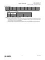
1
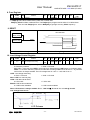
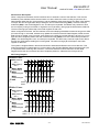
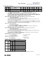
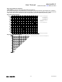
User Manual KSL56M017 16KB MTP ROM 176B RAM I/O MCU Revision History: Date Revision# Description 2013/06/24 005 1. Revise some errors 2013/06/19 004 1. Revise device name to ET56M017 2013/06/13 003 2013/03/05 002 18 4 1. Revise 14 SOP package pin out 4 17 2,3,5 1. Change RAM size to 176B 2. Add PA1PHS register bit to select PA1 pull-high R=10K or 300K 7,9,22 3. Add a register bit to select IR learning edge detect interrupt mode 3,7,9,16 4. Add SPIS register bit to select SPI interface pins 5. Swap PC[1:0] SPI pin function 001 错误!未指定书签。 4,10 2. Revise 16 SOP package pin out 2. Revise some errors 2012/12/25 Page 2~4,7,9,17,18 2~4,9 6. Redefine SPIR[1:0] SCK clock rate 18 7. Add a new 16 SOP package form 4 New create -1- 2013/06/24 User Manual KSL56M017 16KB MTP ROM 176B RAM I/O MCU Features 1. Operate voltage: ¾ 1.8V~3.6V @ 8MHz 2. Built-in Main-clock oscillator 3. 4. 5. 6. 7. 8. ¾ BR8M: Built-in RC 8MHz oscillator with 6 calibration bits (+/- 1%) ¾ XT8M: External crystal 8MHz (No built-in C) 2 kinds of CPU speed: Fcpu=Fosc/1, Fosc/2 2 kinds of CPU operating mode: Normal or Sleep. RV9E CPU core 16K bytes Program MTP ROM 176 bytes General Purpose SRAM 2 timers ¾ Timer 0: 8-bit timer ¾ Timer 1: 8-bit timer 9. 18 I/O pins: ¾ PA0(OPO)*, PA1, PA2(MISO)*, PA3(SSB)*, PA4(OSCI)*, PA5(OSCO)*, PA6(T0CKI)*, PA7(INTX(VPP))* ¾ PB4(REM)*, PY(REM)* ¾ PC0(SCK)*, PC1(MOSI)*, PC[3:2], PC4(SCK)*, PC5(MOSI)*, PC6(MISO)*, PC7(SSB)* *: share pin 10. 7 interrupt sources: ¾ Divide interrupt time-base ¾ Timer 0 interrupt ¾ Timer 1 interrupt ¾ PA interrupt: When the falling edge transition in port A ¾ External interrupt ¾ IR learning input interrupt ¾ SPI interrupt 11. Built-in IR learning function 12. Key scan wake up function 13. SPI function 14. LVR/LVD function 15. COB or 14/16/20 SOP package form 错误!未指定书签。 -2- 2013/06/24 User Manual KSL56M017 16KB MTP ROM 176B RAM I/O MCU Block Diagram OSCI OPO Main-clock Fosc Oscillator (8MHz) OSCO ÷2 1 1 PAi0 Fcpu 0 IRTO RCS0 HALT ÷2 MCB[5:0] 1 F4M 0 ÷128 Fosc32K ÷ 32 F4MSEL Sub-clock Oscillator (35KHz) ÷2 ÷ 64 00 01 PAi2 DIV 10 11 RPU[1:0] GAINS[1:0] Preload Register Reload OPIF IR Learning Circuit IRFLT[1:0] VREFS[1:0] OPON, OPOS PA2_MISO 01 1X SPIS, SPE OPI, OPIS[1:0] KSEN 00 MISOi DIVS[1:0] Fsub PA1 PAi1 Fosc_8K Fosc_16K Fosc_512 Fosc_1K ÷4 OMS0 (FFF8h.0) PA0_OPO 0 PAi3 00X + 1XX SSBi 010 MSSBD 011 PA3_SSB SPIS, SPE, MSTR OPO OSCI 1 PAi4 0 PA4_OSCI OMS0 (FFF8h.0) F4M/4 0 T0CKI 1 T0SEL F4M T0I 0 8-bit Up-count Timer 1 TMR0 1 PAi5 0 PA5_OSCO TMR0S1 OMS0 (FFF8h.0) TMR0ON TMR_SYNC, DIV T0I 1 PAi6 0 PA6_T0CKI Preload Register Reload Fsub KSPNO[1:0] KSPW[1:0] Key Scan Controller T0SEL KEY INTX 1 PAi7 TMR0 0 F4M/128/32 (1KCLK) 1 8-bit Up-count Timer TMR1 PYi LVR/LVD RESET LVRF TMR0/2 (1/2 duty) TMR0/3 (1/3 duty) LVDF 00 01 10 11 IRO IRO 1 PBi4 PB4_REM 0 IROS IRS[1:0] PCi[1:0] MOSIi, SCKi 00 01 PC1_MOSI PC0_SCK 1X DIV TMR0 TMR1 PA INTX OPI SPII PY_REM 0 IRS1=0 + IROS PBi4 LVDS 1 /IRO TMR1ON TMR_SYNC, DIV VDD PA7_INTX 0 PA7S KSEN TMR1S0 ENLVD OSCO RAM 176B SPIS, SPE PCi[3:2] Interrupt IRQ Control PCi[6:4] RV9E core Fosc, SPI2X SPIR[1:0], MSTR I Fcpu RESET MTP ROM 16KB CPOL, CPHA WCOL, DORD SPE SPII, SPIF SPI Controller Circuit SPIS, MSSBD SSBi, SCKi MISOi, MOSIi PC[3:2] PC6_MISO PC5_MOSI 0X PC4_SCK 10 MISOi, MOSIi, SCKi 11 SPIS, SPE PCi7 0XX + 10X SSBi 110 MSSBD 111 PC7_SSB SPIS, SPE, MSTR 错误!未指定书签。 -3- 2013/06/24 KSL56M017 User Manual 16KB MTP ROM 176B RAM I/O MCU Pad Description Name PC7_SSB, PC6_MISO, PC5_MOSI, PC4_SCK, PC3 PC2,PC1_MOSI, PC0_SCK I/O PB4_REM O PY_REM I/O Description Bi-directional 8-bit I/O port. It can be configured as CMOS output or input. PC7_SSB, PC6_MISO, PC5_MOSI, PC4_SCK, PC1_MOSI and PC0_SCK also shared with SPI pins. 1-bit O/P port. It can be configured as CMOS or NMOS output. PB4_REM also shared with IR output function. I/O VDD, VSS, VSS Bi-directional 1-bit I/O port. It can be configured as CMOS output or input with or without pull-high resistor. PY_REM also shared with IR output. P PA6_T0CKI, PA5_OSCO, PA4_OSCI, PA3_SSB, PA2_MISO, PA1, PA0 Power supply 7-bit I/O port. It can be configured as output port (CMOS or NMOS output) or input port (with or without pull-high resistors). PA6_T0CKI also shared with external clock T0CKI input function. PA5_OSCO & PA4_OSCI also shared with main oscillator clock pins. PA3_SSB and PA2_MISO also shared with SPI chip select and data I/O pins. 1-bit input port. It can be configured as input with or without pull-high resistors. PA7_INTX_VPP also shared with external interrupt and program mode high voltage input function. I/O VDD PC7_SSB PC6_MISO PC5_MOSI PC4_SCK I PB4_ REM PA7_INTX_VPP 21 20 19 18 17 1 22 VSS 16K X8 MTP PB4_REM 16 PC3 15 PC2 14 PC1_MOSI 13 PC0_SCK 12 PA3 _SSB 11 PA2 _MISO 2 4 PA5_OSCO 5 6 7 8 9 10 PA1 PA4_OSCI PA0 3 PY_REM VSS PA7_INTX_VPP (0, 0) PA6_T0CKI No. ps: The pad location is for reference only. Please do not apply it to PCB layout. VDD PB4_REM PC7_SSB PC6_MISO PC5_MOSI PC2 PC1_MOSI PC0_SCK PY_REM PA7_INTX_VPP PA6_T0CKI PA5_OSCO PA4_OSCI VSS PB4_REM VDD VDD PB4_REM PC7_SSB PC6_MISO PC5_MOSI PC4_SCK PC3 PC2 PC1_MOSI PC0_SCK 56M017 14-SOP 56M017 16-SOP 56M017 16-SOP 56M017 20-SOP VSS PA4_OSCI PA5_OSCO PA6_T0CKI PA7_INTX_VPP PY_REM PA2_MISO PA3_SSB PA2_MISO PA3_SSB PC0_SCK PC1_MOSI PC4_SCK PC5_MOSI PC6_MISO PC7_SSB VSS PA4_OSCI PA5_OSCO PA6_T0CKI PA7_INTX_VPP PY_REM PA0 PA1 PA2_MISO PA3_SSB 20SOP Pin Assignment VDD PB4_REM PC7_SSB PC6_MISO PC5_MOSI PC4_SCK PA3_SSB 16SOP Pin Assignment VSS PA6_T0CKI PA7_INTX_VPP PY_REM PA0 PA1 PA2_MISO 14SOP Pin Assignment 错误!未指定书签。 -4- 2013/06/24 User Manual KSL56M017 16KB MTP ROM 176B RAM I/O MCU 1. Memory Mapping Address Content Comment 0000h - 002Fh Special Register 0030h - 007Fh Reserved 0080h - 00FFh Mapping To 1800h - 187Fh Data RAM 0100h - 01AFh Mapping To 1800h - 18AFh Stack 01B0h - 07FFh Reserved 0800h - 0FFFh Mapping To 1800h - 1FFFh Low Nibble 0Xh 1000h - 17FFh Mapping To 1800h - 1FFFh High Nibble 0Xh 1800h - 18AFh General Purpose RAM 176B 18B0h - 1FFFh Reserved 2000h - 3FFFh Mapping To C000h - DFFFh 4000h - 7FFFh Reserved 8000h - BFFFh Reserved C000h - DFEFh Program MTP ROM 8KB (Read only) E000h - FFEFh Program MTP ROM 8KB - 16B (Read only) FFF0h - FFF7h System Configure ROM FFF8h - FFF9h Code Option FFFAh - FFFBh Reserved FFFCh - FFFDh Reset Vector FFFEh - FFFFh IRQ Vector 8KB (Read / Write) System area* 2. RAM Mapping Logical Address 0080h 0100h 00FFh 017Fh 0180h 01AFh 错误!未指定书签。 1800h 187Fh 1880h 18AFh Size 128B 48B Physical Address 1800h 187Fh 1880h 18AFh -5- Comment For zero page RAM and Stack (sharing) For Data RAM and Stack (sharing) 2013/06/24 User Manual KSL56M017 16KB MTP ROM 176B RAM I/O MCU 3. Code Option Address FFF8h FFF9h b7 - b6 - b5 - b4 - b3 - b2 - b1 - b0 OMS0 PROTB OMS0: Main oscillator mode select 0= XT8M 1= BR8M Pad Function Main Oscillator OMS0 Mode PA4_OSCI PA5_OSCO 0 XT8M OSCI OSCO 1 BR8M PA4 PA5 PROTB(FFF9h.0): Protect program ROM option 0: Program ROM is protected. Enter program mode can not read ROM from program data pin but the Code Option bytes data can still read out even PROTB=0. Data can write into both program ROM and Code Option bytes except PROTB bit. 1: Program ROM is unprotected. Enter program mode can read ROM from program data pin. 错误!未指定书签。 -6- 2013/06/24 User Manual KSL56M017 16KB MTP ROM 176B RAM I/O MCU 4. Special Registers ADR NAME R/W 00h TEST - 01h PA 02h PAWAKE 04h PADIR 05h PB 06h PBTYPE Content Reserved b7 b6 b5 b4 b3 b2 b1 b0 - - - - - - - - R/W PA Data Reg. PAD[7:0] R/W Wakeup Mask Reg. Value on POR ---- ---1111 1111 PAW[7:2] PAC[6:2] PAW[1:0] 0000 0000 PAC[1:0] -111 1111 R/W PA Direction Reg. - R/W PB Data Reg. - PYD - PBD4 - - - - -0-1 ---- R/W PB Output Type Reg. - PYC - PBT4 - - - - -1-0 ---- 07h PC R/W PC Data Reg. PCD[7:0] 1111 1111 08h PCDIR R/W PC Direction Reg. PCC[7:0] 1111 1111 0Ch PADF0 R/W Pad Function CTRL 0 Reg. 0Dh PADF1 0Eh - IROS - IRS1 PA1 IRS0 PA7S -0-0 00-- - - ---0 ---- DIVI --00 -000 DIVF --00 -000 - - - IER R/W Interrupt Enable Reg. - - INTX PAI - 0Fh IFR R/W Interrupt Request Flag Reg. - - INTF PAF - 10h TMR0 R/W Timer 0 Data Reg. TMR0[7:0] xxxx xxxx 12h TMR1 R/W Timer 1 Data Reg. TMR1[7:0] xxxx xxxx 16h TMRC R/W Timer Control Reg. - 17h TMCLK R/W Timer Clock Reg. - 18h DIVC R/W Divider Control Reg. - 1Dh SYSCLK R/W System Clock Select Reg. - T0 SEL TMR_ SYNC F4M SEL 1Eh HALT W CPU HALT Control Reg. 2Dh OPC0 R/W OP/COMP Control 0 Reg. RPUS[1:0] 2Eh OPC1 R/W OP/COMP Control 1 Reg. OPO OPIS0 2Fh MF 32h SPCR 33h SPSR R/W SPI Status Reg. R/W SPI Data Reg. TMR1 TMR0 I I TMR1 TMR0 F - - - - - - - - - - - - RCS0 - - F TMR1 TMR0 ON TMR1 TMR0 S0 S1 ON - DIVS1 DIVS0 - - -0-- --00 ---- -xx-0-- --xx -1-1 ---xxxx xxxx R/W Miscellaneous Function Reg. R/W SPI Control Reg. - - R/W Pad Function CTRL 1 Reg. PHS - - GAINS[1:0] OPI IRFLT[1:0] VREFS[1:0] 1001 1010 OPIF OPON OPOS OPIS1 IRTO x000 0x00 MCB[5:0] SPII - - SPE DORD MSTR CPOL CPHA SPIR1 SPIR0 SPIF WCOL - - MSSB D - SPIS SPI2X SPD[7:0] 1000 00-0000 0000 00-- 1-x0 34h SPDR 3Ah PAK R/W PA Key Scan Control Reg. PAK7 PAK6 PAK5 PAK4 PAK3 PAK2 PAK1 PAK0 3Bh PBK R/W PB Key Scan Control Reg. KSEN PYK KSPNO[1:0] 0x-- xxxx 3Ch PCK R/W PC Key Scan Control Reg. PCK7 PCK6 PCK5 PCK4 PCK3 PCK2 PCK1 PCK0 xxxx xxxx 3Dh LVC R/W Low Voltage Control Reg. 3Eh FUSE R Fuse Reg. 4Fh WS R Wait State Select Reg. EN - LVD - - xxxx xxxx KSPW[1:0] LVDS LVDF LVRF - FSA[5:0] - - - - - - xxxx xxxx - - 0-x0 1--- - - aaaa aa--* BUSY ---- --00 WR FAIL 1 *1: FSA[5:0] POR value: Determined by wafer CP or Writer data. 错误!未指定书签。 -7- 2013/06/24 KSL56M017 User Manual 16KB MTP ROM 176B RAM I/O MCU 5. Port A, Port B, Port C ADR NAME 01h 02h R/W PA Content b7 b6 b5 R/W PA Data Reg. 04h PADIR 05h PB 06h PBTYPE 07h PC 08h PCDIR 1111 1111 PAW[1:0] 0000 0000 PAC[1:0] -111 1111 - PYD - PBD4 - - - - -0-1 ---- R/W PB Output Type Reg. - PYC - PBT4 - - - - -1-0 ---- PAC[6:2] R/W PC Data Reg. PCD[7:0] 1111 1111 R/W PC Direction Reg. PCC[7:0] 1111 1111 Register Read Write PA/PB/PC PAWAKE 1: Selected Pull-High PA7 is input only 0: output logic Low PB used as output only 1: output logic High 0: bit n is none wakeup 1: bit n is wakeup Register Data PBTYPE Register Data PADIR/ PBTYPE/PCDIR Register Data Comment 0: Selected Tri-state Pad Data 1 Æ 0 (Falling edge) Wakeup 0: bit n is NMOS Output Port PA=O/P 04h/06h.6/08h Value on POR b0 R/W PA Direction Reg. PA=I/P 06h.4 b1 PAW[7:2] O/P Register Data 02h b2 R/W PB Data Reg. I/P 01h/05h/07h b3 PAD[7:0] PAWAKE R/W Wakeup Mask Reg. ADR b4 1: bit n is CMOS Output Port 0: bit n is NMOS Output Port NMOS or CMOS for output port 1: bit n is CMOS Output Port 0: bit n is Output Port PC & PY output mode is CMOS only. 1: bit n is Input Port Note: 1. PB4 is an output only port. PBT4 defines PB4 output type is CMOS or NMOS. 2. PY is an I/O port. PYC controls PY I/O direction. PA_WAKEUP DATABUS PORT C PY PORT A D DATABUS D Q WRITE I/O Q CK WRITE I/O OUTPUT MODE CK OUTPUT MODE Weak 300K INPUT MODE INPUT MODE Weak 300K READ I/O KEY IRQ PA_WAKEUP READ I/O DATABUS CMOS TYPE D Q WRITE I/O CK PORT B READ I/O I/O Port Summary PA[6:0] PA7 PB PC PY Input Function Pull-High Tri-state Wakeup V V V V V V V V V V - Output Function CMOS NMOS V V V V V V - The Pull-High supply voltage must <VDD+0.7V when NMOS Open-drain output. 错误!未指定书签。 -8- 2013/06/24 KSL56M017 User Manual 16KB MTP ROM 176B RAM I/O MCU Pad Function Definition ADR NAME R/W 0Ch PADF0 0Dh Value on b7 b6 b5 b4 b3 b2 b1 b0 R/W Pad Function CTRL 0 Reg. - IROS - IRS1 IRS0 PA7S - - -0-0 00-- PADF1 R/W Pad Function CTRL 1 Reg. - - - - - - - ---0 ---- 16h TMRC R/W Timer Control Reg. - - - 2Eh OPC1 R/W OP/COMP Control 1 Reg. OPO OPIS0 R/W SPI Control Reg. SPII SPE 32h SPCR 33h SPSR Content SPIF R/W SPI Status Reg. T0 SEL PA1 PHS - - OPI OPIF POR TMR1 TMR0 ON -0-- --00 ON OPON OPOS OPIS1 IRTO x000 0x00 DORD MSTR CPOL CPHA SPIR1 SPIR0 0000 0000 WCOL - - MSSB D - SPIS SPI2X 00-- 1-x0 I/O Port Operating Mode Select PAD Name PA7_INTX_VPP PA6_T0CKI PA5_OSCO PA4_OSCI PA3_SSB, PA2_MISO PA1 PA0_OPO PB4_REM PY_REM Register Bit PA7S T0SEL OMS0 (FFF8h.0) OMS0 (FFF8h.0) SPIS, SPE PA1PHS IRTO IROS, IRS1, IRS0 IROS, IRS1, IRS0 PC7_SSB, PC6_MISO, PC5_MOSI, PC0_SCK Note 0 PA7 1 INTX External interrupt pin, falling edge trigger X VPP PA7_INTX_VPP > 5V will enter program mode. 0 PA6 1 T0CK I 0 OSCO 1 PA5 0 OSCI T0CKI input 1 PA4 00 or 1X PA[3:2] 01 SSB, MISO 0 PA1 Pull-high R=300K Ohm if PA1 set as input with pull-high R. 1 PA1 Pull-high R=10K Ohm if PA1 set as input with pull-high R. 0 PA0 1 OPO 0XX PB4 100 PB4 101 PB4 110 TMR0/2 (1/2 duty) 111 TMR0/3 (1/3 duty) 000 PY SPI SSB and MISO function IOL=6mA @ VOL=0.3V IOL=320mA @ VOL=1.5V 001 PY 010 TMR0/2 (1/2 duty) 011 TMR0/3 (1/3 duty) 1XX PY 0X or 10 PC[7:4] IR output, IOL=320mA @ VOL=1.5V IR output SPIS, SPE 11 PC4_SCK PC1_MOSI, Pad Function SPIS, SPE 错误!未指定书签。 SSB, MISO, MOSI, SCK 00 or 1X PC[1:0] 01 MOSI, SCK -9- SPI SSB, MISO, MOSI and SCK function SPI MOSI and SCK function 2013/06/24 User Manual KSL56M017 16KB MTP ROM 176B RAM I/O MCU 6. MTP ROM Write ADR NAME R/W 4Fh WS R Content b7 b6 b5 B4 b3 b2 Wait State Select Reg. - - - - - - BUSY: MTP ROM write busy flag 0 = No write operation is running 1 = Write operation is running WRFAIL: MTP ROM write pass or fail flag 0 = No write operation is failed 1= Write operation is failed b1 b0 WRFAIL BUSY Value on POR ---- --00 BUSY and WRFAIL flags are read only. The two flags are used for checking lower 8KB (C000h - DFFFh) MTP write status. While the data is writing into the lower 8KB MTP ROM, BUSY flag will set. When BUSY=1, user can access the upper 8KB (E000h - FFFFh) MTP ROM but can not access the lower 8KB MTP ROM until the write operation is completed. After MTP write operation is completed, hardware will clear the BUSY flag automatically. The MTP typical write time, Twr, is 1ms @ 3.3V. If write operation is failed, the WRFAIL flag will be set and the BUSY flag will be cleared at the same time. User can try to write the same location of the MTP ROM again for it may be successful at the second write. MTP Program Mode PA7_INTX_VPP pin force high voltage, 8V, will enter program mode. PA5 is used for check the program mode is in progress or not. Force PA7_INTX_VPP pin to VDD can leave program mode and the hardware will generate another one shot pulse to reset the chip again. In program mode, PA3 is used for clock input pin and PA2 is used as data in/out pin. MTP ROM Program Mode PAD Name Normal Mode Program Mode PA7_INTX_VPP PA7_INTX_VPP < 5V PA7_INTX_VPP (Typ. 8V) > 5V PA2 PA2 I/O pin for program data transfer. PA3 PA3 Input pin with pull-high for program clock inputs. PA5 PA5 Output pin. Clock signal is output to PA5 for writer check. Program Mode Application Block Diagram WRITER VPP 56M017 PA7_INTX_VPP DATA PA2 CLK PA3 PGM_CHK PA5 错误!未指定书签。 - 10 - 2013/06/24 KSL56M017 User Manual 16KB MTP ROM 176B RAM I/O MCU 7. Oscillator, Fosc & Fcpu ADR NAME R/W 1Dh SYSCLK 2Fh MF Content b7 R/W System Clock Select Reg. - b6 F4M SEL R/W Miscellaneous Function Reg. RCS0: Fsys-Clock select 0: Fsys=Fosc/1 b5 B4 RC - S0 MCB[5:0] 1: Fsys=Fosc/2 OMS0 (FFF8h.0) F4MSEL: F4M select 0: F4M=Fosc/1 1: F4M=Fosc/2 MCB[5:0]: Main-clock calibration bits MCB[5:0] 00h 001 … 1Fh 20h 21h 22h … 3Fh Adjust Percentage +32% +31% … +1% 0% -1% -2% -31% Value on b3 b2 b1 b0 - - - - -1-1 ---- - - 1000 00-- PA5_OSCO, PA4_OSCI PAD Function POR Fosc Mode 0 OSCO, OSCI XT mode 1 PA5, PA4 BR mode Frequency After Adjusted Fosc = Forg x (1+0.32) Fosc = Forg x (1+0.31) Fosc = Forg x (1+0.01) Fosc = Forg (Forg is non-adjusted freq. Target is 8MHz.) Fosc = Forg x (1-0.01) Fosc = Forg x (1-0.02) Fosc = Forg x (1-0.31) Fcpu Timing Diagram Fcpu=Fsys Fosc tDelay Fcpu CPU HALT CPU Wakeup tDelay: tDelay = 4Fcpu (BR8M) or 1024Fosc (XT8M) 错误!未指定书签。 - 11 - 2013/06/24 KSL56M017 User Manual 16KB MTP ROM 176B RAM I/O MCU 8. Fuse Register ADR NAME R/W 3Eh FUSE R Content b7 b6 b5 Fuse Reg. B4 b3 b2 b1 b0 - - FSA[5:0] Value on POR aaaa aa--*1 *1: FSA[5:0] POR value: Determined by wafer CP or Writer data. FSA[5:0]: BR8M oscillator calibration bits. The FSA[5:0] are programmed at wafer CP or Writer data. User can load FSA[5:0] then write to MCB[5:0] to get high accuracy BR8M frequency. 9. RESET LVR or POR Reset Power On Reset (PWR) VDD RESET Low Voltage Reset (LVR) Fosc x 2^17 (~16ms) RESET INTERNAL RESET Main Oscillator OFF CPU running Main Oscillator ON RESET Block Diagram Reset Timing Diagram 10. Low Voltage Control Register ADR 3Dh NAME LVC R/W Content b7 EN R/W Low Voltage Control Reg. LVD B6 - b5 B4 b3 LVDS LVDF LVRF b2 b1 b0 - - - Value on POR 0-x0 1--- LVRF: Power-on or low voltage reset flag 0: Cleared by software 1: VDD < LVR level While VDD < LVR level, the LVRF is set to logic high. Otherwise the LVRF keeps un-changed. When LVRF=1, it must be cleared by software for next time checking. LVRF cannot be set to ‘1’ by software. LVR function is always enabled. The LVR voltage level is 1.65V +/- 10% with Vh=0.1V. LVDF: Low voltage detect flag 0: VDD > LVD level Note: LVDF is a read only flag. LVDS: LVD detect level select 0: LVD=2.05V 1: LVD=2.25V ENLVD: LVD function enable bit 0= LVD function disabled 1= LVD function enabled 1: VDD < LVD level Note: LVR function is always enabled. VLVR = 1.65V ±10%, VH = 0.1V. ILVR = 1.0uA @ VDD=3V. Low Voltage Reset Curve VLVR 错误!未指定书签。 LVR Release - 12 - 2013/06/24 KSL56M017 User Manual 16KB MTP ROM 176B RAM I/O MCU 11. CPU HALT ADR NAME 1Eh HALT R/W Content b7 b6 b5 B4 b3 b2 b1 Value on b0 POR W CPU HALT Control Reg. xxxx xxxx When writing into address HALT, CPU will go into sleep mode. When in sleep mode, all kinds of interrupt sources can wake up CPU, but IER need to be set to '1'. CPU Operating Mode Clock Status CPU Operating Mode Actions Fcpu Fosc 1. Write the HALT register Sleep OFF OFF 1. Wakeup from HALT state 2. Start from RESET Normal Fsys ON Note Turn-off all and Istb<1uA Normal speed. Note: The Fcpu will be turned off after write HALT register. 12. Divider The Divider can be used as time base or clock input sampling rate. ADR NAME R/W 18h DIVC R/W Divider Control Reg. DIVS1 0 0 1 1 DIVS0 0 1 0 1 错误!未指定书签。 Content b7 - b6 TMR_ SYNC b5 b4 b3 b2 - - - - b1 Value on b0 POR DIVS1 DIVS0 -0-- --xx Divider Clock F4M/128/4 (8KHz) F4M/128/2 (16KHz) F4M/128/64 (512Hz) F4M/128/32 (1KHz) - 13 - 2013/06/24 KSL56M017 User Manual 16KB MTP ROM 176B RAM I/O MCU 13. Timer 0,1 ADR NAME R/W Content 10h TMR0 R/W Timer 0 Data Reg. 12h TMR1 R/W Timer 1 Data Reg. b7 b6 b5 b4 b3 b2 b1 TMR0[7:0] 16h TMRC R/W Timer Control Reg. - 17h TMCLK R/W Timer Clock Reg. - 18h DIVC R/W Divider Control Reg. - SEL TMR_ SYNC - - - - - - - - - POR xxxx xxxx TMR1[7:0] T0 Value on b0 xxxx xxxx TMR1 TMR0 - ON TMR1 TMR0 S0 - -0-- --00 ON S1 - ---- -xx- DIVS1 DIVS0 -0-- --xx TMR0[7:0]: Timer 0 data register. TMR1[7:0]: Timer 1 data register. TMR0ON: 1= Timer 0 ON 0= Timer 0 OFF TMR1ON: 1= Time 1 ON 0= Timer 1 OFF T0SEL: TMR0 clock source select 0= T0I = F4M4 1= T0I = T0CKI Note: T0CKI is falling edge trigger. TMR_SYNC: TMR0 & TMR1 ON/OFF sync control bit 0= Asynchronous 1= Sync with DIV While TMR_SYNC=1, the TMR0 & TMR1 are synchronized by DIV. Set/clear TMR1ON and TMR0ON, TMR1 and TMR0 will not start/stop counting until DIV occurs. TMR0S1: TMR0 clock source select 0= F4M 1= T0I TMR1S0: TMR1 clock source select 0= TMR0 1= F4M/128/32(1KCLK) Timer 0, 1 are up-count timers. When time out (FFh Æ 00h) will set TMRF flag, request IRQ interrupt and reload the initial value from Preload Register at same time. When Timer 0, 1 are off that Data write to Preload Register & Timer. When time is on Data write to Preload Register, until time out that data write to timer from Preload register. Preload Register F4M F4M/4 T0CKI 0 T0I 0 1 8-bit Up-count Timer Reload Preload Register TMR0 TMR0 F4M/128/32 (1KCLK) 1 TMR0S1 T0SEL TMR0ON TMR1S0 TMR_SYNC, DIV Timer 0 错误!未指定书签。 0 1 8-bit Up-count Timer Reload TMR1 TMR1ON TMR_SYNC, DIV Timer 1 - 14 - 2013/06/24 User Manual KSL56M017 16KB MTP ROM 176B RAM I/O MCU 14. IR Output Function ADR NAME R/W Content 0Ch PADF0 R/W Pad Function CTRL 0 Reg. b7 b6 b5 b4 b3 b2 b1 b0 - IROS - IRS1 IRS0 PA7S - - Value on POR -0-0 00-- A. IR output from PY PY can be used as IR output pin. It is high-active. The PY is input tri-state at POR initial. The application circuit is shown as in the right diagram. IROS 0 0 0 0 1 IRS1 0 0 1 1 X IRS0 0 1 0 1 X Pad Function PY PY IR output (TMR0/2, 1/2 duty) IR output (TMR0/3, 1/3 duty) PY PY The carrier output sequences are a. PY set to CMOS output and output ‘0’. b. IROS cleared as ‘0’. c. IRS[1:0]=10 or 11 for active IR carrier output. (PY output low while TMR0 off.) d. IRS1=0 for in-active IR carrier output. B. IR output from PB4 The PB4 can be used as IR output pin. It is low-active. The application circuit is show as in right diagram. IROS IRS1 IRS0 Pad Function 0 X X PB4, IOL=6mA @ VOL=0.3V 1 0 0 PB4, IOL=320mA @ VOL=1.5V 1 0 1 PB4, IOL=320mA @ VOL=1.5V 1 1 0 IR output (TMR0/2, 1/2 duty), IOL=320mA @ VOL=1.5V 1 1 1 IR output (TMR0/3, 1/3 duty), IOL=320mA @ VOL=1.5V PB4 The carrier output sequences are I. IROS set to ‘1’. II. IRS[1:0]=10 or 11 for active IR carrier output. (PB4 output high while TMR0 off.) III. IRS1=0 for in-active IR carrier output. The IR carrier duty is 1/2 in frequency out from TMR0/2, the other is 1/3 and out from TMR0/3. The output waveform is show as below. IR Output Data Carrier output 1/2 Duty or 1/3 Duty (PB4 low active) or 1/3 Duty (PY high active) 错误!未指定书签。 TMR0/2 TMR0/3 TMR0/3 - 15 - 2013/06/24 KSL56M017 User Manual 16KB MTP ROM 176B RAM I/O MCU 15. IR Learning Function ADR NAME R/W Content b7 2Dh OPC0 R/W OP/COMP Control 0 Reg. 2Eh OPC1 R/W OP/COMP Control 1 Reg. b6 RPUS[1:0] OPO OPIS0 RPUS[1:0]: Input resistor select 00: RH = 0.85Rx 01: RH = 1.15Rx GAINS[1:0]: OP1 gain select 00: Gain = 2 01: Gain = 3 IRFLT[1:0]: IR input digital filter select 00 = 20ns 01 = 40ns VREFS [1:0]: COMP reference voltage select 00: Vref=VDD-0.5Vx 01: Vref=VDD-0.4Vx OPO: IR output data (Read only) OPIS[1:0]: OPO interrupt select 00 = OPO falling edge interrupt 1X = OPO falling and rising edge interrupt OPI: OPO interrupt enable bit 0 = Disable OPO interrupt OPIF: OPO interrupt flag bit 0 = No OPO interrupt occurs OPON: OP ON/OFF bit 0 = OP OFF OPOS: OP output select 0: OPO = CMPO b5 b4 GAINS[1:0] OPI b3 b2 IRFLT[1:0] b1 b0 VREFS[1:0] OPIF OPON OPOS OPIS1 IRTO Value on POR 1001 1010 x000 0x00 10: RH = Rx 11: RH = 0.7Rx 10: Gain = 4 11: Gain = 5 10 = 80ns 11 = 150ns 10: Vref=VDD-0.3Vx 11: Vref=VDD-0.2Vx 01 = OPO rising edge interrupt 1 = Enable OPO interrupt 1 = OPO interrupt occurs 1 = OP ON 1: OPO = PXO Pulse Extension Circuit is used to extend CMPO pulse to guarantee each PXO output low pulse width greater than 8us. If CMPO low pulse width less than 8us, the PXO low pulse width will be 8us. If CMPO low pulse width larger than 8us, the PXO follows the CMPO output. IRTO: IR learning output to pad select 0 = OPO can not output to pad 1 = OPO can output to PA0 pad Vref=VDD-0.5Vx, VDD-0.4Vx, VDD-0.3Vx or VDD-0.2Vx OPON Vref CMPO RH 0 OPOFF PB4_REM 1 IRO 0 PBi4 OPON PXO IRFLT[1:0] OPOS IROS PY_REM 1 0 OPO 1 PYi OPON IRO OPOFF IRS[1:0]=00 + IROS PA0_OPO 1 0 OPO OPO OPIS[1:0] OPIF OPI PAi0 IRTO 错误!未指定书签。 - 16 - 2013/06/24 KSL56M017 User Manual 16KB MTP ROM 176B RAM I/O MCU 16. Interrupt ADR NAME 0Eh IER R/W Content b6 b5 b4 b3 - - INTX PAI - TMR1I TMR0I - - INTF PAF - TMR1F TMR0F DIVF --00 -000 OPO OPIS OPI OPIF OPON OPOS x000 0x-0 CPOL CPHA MSSBD - R/W Interrupt Enable Reg. 0Fh IFR 2Eh OPC1 R/W Interrupt Request Flag Reg. 32h SPCR R/W SPI Control Reg. SPII SPE 33h SPSR R/W SPI Status Reg. SPIF WCOL R/W OP/COMP Control 1 Reg. DORD MSTR - - b2 b1 Value on b7 - b0 POR DIVI --00 -000 IRTO SPIR1 SPIR0 0000 0000 SPIS SPI2X 00-- 1-x0 IER bit n=1: Enable interrupt IER bit n=0: Disable interrupt DIVI: Divider interrupt TMR0I: Timer 0 interrupt TMR1I: Timer1 interrupt, for real time clock PAI: Port A wakeup interrupt INTX: External input interrupt from PA7 OPI: OPO edge trigger interrupt SPII: SPI interrupt When interrupt happened, the relative IFR will be set to '1'. If IER is set to enable the interrupt, it will request to go into interrupt service routines. Before it goes into Interrupt Service Routine (ISR), the hardware will automatically set the I* bit to '1' to prevent interrupt from occurring again. Within ISR, user needs to judge from IFR to decide which kind of interrupts. Once it is decided, IFR needs to be clear to 0 by program. If there are two interrupt source requests happening simultaneously, the priority should be decided by program. When the first interrupt request is done from RTI, the next interrupt will happening right away. These procedures should be repeated until all interrupts are taking care. User could ‘CLI’ in ISR for enable nest interrupt. PS: The ‘I bit’ is a global interrupt mask bit, set by ‘SEI’, clear by ‘CLI’. EX. .page0 IFRBuf .ends .code IRQ: IFR.0 DS 1 ;use in ISR only DIV IER.0 IFR.1 TMR0 PHA LDA AND STA BBS1 BBS2 BBS0 BBS4 BBS6 BRA IER.1 IER IFR IFRBuf IFRBuf, tmr0irq IFRBuf, tmr1irq IFRBuf, divirq IFRBuf, pairq IFRBuf, lcdirq extirq IFR.2 TMR1 IER.2 PA IER.4 IFR.5 INTX IFR RMB1 …… BRA IFR RMB1 …… IFR WAKEUP I IER.5 divirq: RMB0 …… BRA WAKEUP IFR.4 IRQ OPC1.4 OPI OPC1.5 extirq SPSR.7 tmr0irq: SPII SPCR.7 extirq …… lcdirq: extirq: PLA RTI .ends 错误!未指定书签。 - 17 - 2013/06/24 KSL56M017 User Manual 16KB MTP ROM 176B RAM I/O MCU 17. SPI Function ADDR NAME Content b7 b6 b5 b4 b3 b2 b1 b0 32h SPCR SPI Control Reg. SPII SPE DORD MSTR CPOL CPHA SPIR1 SPIR0 SPIF WCOL - - MSSBD - SPIS SPI2X 33h SPSR SPI Status Reg. 34h SPDR SPI Data Reg. SPD[7:0] SPE: SPI enable 0 = Disable Value on POR 0000 0000 00-- 1-x0 xxxx xxxx 1 = Enable SPIS: SPI interface pins select 0 = PA3_SSB, PA2_MISO, PC1_MOSI, PC0_SCK are selected 1 = PC7_SSB, PC6_MISO, PC5_MOSI, PC4_SCK are selected DORD: SPI data order 0 = MSB transmitted first 1 = LSB transmitted first MSTR: SPI master/slave select 0 = Slave 1 = Master CPOL: SPI clock polarity 0 = Normal low when idle 1 = Normal high when idle CPHA: SPI clock phase 0 = Leading edge sampling 1 = Trailing edge sampling CPOL and CPHA Functionality SPI Mode CPOL CPHA 0 0 0 1 0 1 2 1 0 3 1 1 Leading Edge Sample (Rising) Setup (Rising) Sample (Falling) Setup (Falling) Trailing Edge Setup (Falling) Sample (Falling) Setup (Rising) Sample (Rising) SPIR[1:0]: SPI clock rate select SPI2X: Double SPI speed select SPIR[1 :0] 00 01 10 11 SCK Frequency SPI2X=0 SPI2X=1 Fosc / 2 Fosc / 1 Fosc / 8 Fosc / 4 Fosc / 32 Fosc / 16 Fosc / 64 Fosc / 32 MSSBD: SPI Master mode SSB output data. While configured as SPI Master and SPE=1, PA3_SSB or PC7_SSB pin will be as SPI Master SSB output. The output data of SSB pin refers to MSSBD register bit setting. MSSBD=1 SSB pin output high and MSSBD=0 SSB pin output low. While configured as SPI Slave or SPE=0, the register bit is ignored. WCOL: SPI write collision flag. This bit is read only. The WCOL bit is set if the SPI Data Register (SPDR) is written during a data transfer. The WCOL bit is cleared by first reading the SPI Status Register with WCOL set, and then accessing the SPI Data Register. SPD[7:0]: SPI data The SPI Data Register is a Read/Write Register used for data transfer between the register file and the SPI Shift Register. Writing to the register initiates data transmission. Reading the register causes the Shift Register Receive buffer to be read. 错误!未指定书签。 - 18 - 2013/06/24 User Manual KSL56M017 16KB MTP ROM 176B RAM I/O MCU SPI Function Description When configured as a Master, the SPI interface has no automatic control of the SSB line. This must be handled by user software before communication can start. When this is done, writing a byte to the SPI Data Register starts the SPI clock generator, and the hardware shifts the 8 bits into the Slave. After shifting one byte, the SPI clock generator stops, setting the end of transmission flag (SPIF). If the SPI interrupt enable bit (SPII) in the SPCR Register is set, an interrupt is requested. The Master may continue to shift the next byte by writing it into SPDR, or signal the end of packet by driving high the Slave Select, SSB line. The last incoming byte will be kept in the buffer register for later use. When configured as a Slave, the SPI interface will remain sleeping with MISO tri-stated as long as the SSB pin is driven high. In this state, software may update the contents of the SPI Data Register, SPDR, but the data will not be shifted out by incoming clock pulses on the SCK pin until the SSB pin is driven low. As one byte has been completely shifted, the end of transmission flag (SPIF) is set. If the SPI interrupt enable bit (SPII) in the SPCR Register is set, an interrupt is requested. The Slave may continue to place new data to be sent into SPDR before reading the incoming data. The last incoming byte will be kept in the buffer register for later use. The system is single buffered in the transmit direction and double buffered in the receive direction. This means that bytes to be transmitted can not be written to the SPI Data Register before the entire shift cycle is completed. When receiving data, however, a received character must be read from the SPI Data Register before the next character has been completely shifted in. Otherwise, the first byte is lost. SPI Timing Diagram CPHA=0 Case: SCK (CPOL=0) Mode 0 SCK (CPOL=1) Mode 2 MOSI / MISO Input Sampled MOSI Output Changed MISO Output Changed SSB DORD=0 MSB Bit 6 Bit 5 Bit 4 Bit 3 Bit 2 Bit 1 LSB DORD=1 LSB Bit 1 Bit 2 Bit 3 Bit 4 Bit 5 Bit 6 MSB CPHA=1 Case: SCK (CPOL=0) Mode 1 SCK (CPOL=1) Mode 3 MOSI / MISO Input Sampled MOSI Output Changed MISO Output Changed SSB DORD=0 MSB Bit 6 Bit 5 Bit 4 Bit 3 Bit 2 Bit 1 LSB DORD=1 LSB Bit 1 Bit 2 Bit 3 Bit 4 Bit 5 Bit 6 MSB 错误!未指定书签。 - 19 - 2013/06/24 KSL56M017 User Manual 16KB MTP ROM 176B RAM I/O MCU 18. Key Scan Function ADR NAME R/W 3Ah Content b7 b6 b5 b4 b3 b2 b1 b0 PAK6 PAK5 PAK4 PAK3 PAK2 PAK1 PAK0 PAK R/W PA Key Scan Control Reg. PAK7 3Bh PBK R/W PB Key Scan Control Reg. KSEN PYK - - 3Ch PCK R/W PC Key Scan Control Reg. PCK7 PCK6 PCK5 PCK4 KSPW[1:0] PCK3 PCK2 KSPNO[1:0] PCK1 PCK0 Value on POR xxxx xxxx 0x-- xxxx xxxx xxxx KSEN: Key scan function enable bit 0: Disable key scan function 1: Enable key scan function While KSEN=1, the internal BR35K is automatically turned on and starts to oscillation. While KSEN=0, BR35K is turned off immediately. PA[7:0], PY, PC[7:0] are used as normal I/O function. The PAK7, PAK6, PAK5, PAK4, PAK3, PAK2, PAK1, PAK0, PYK, PCK7, PCK6, PCK5, PCK4, PCK3, PCK2, PCK1 and PCK0 register bit settings are ignored. PAK7, PAK6, PAK5, PAK4, PAK3, PAK2, PAK1, PAK0: PA[7:0] key scan function select 0: PA used as normal I/O 1: PA used as keyboard scan output line or return line PAK7, PAK6, PAK5, PAK4, PAK3, PAK2, PAK1 and PAK0 control PA7, PA6, PA5, PA4, PA3, PA2, PA1 and PA0 function respectively. In key scan mode, i.e. KSEN=1, if PAn (n=0~7) is an input only function and PAKn=1, PAn is used as keyboard scan return line. If PAn is an I/O function and PAKn=1, PAn will output low in its scan cycle and act as keyboard scan return line in the remaining cycles. PYK: PY key scan function select 0: PY used as normal I/O 1: PY used as keyboard scan output line or return line In key scan mode, i.e. KSEN=1, and PYK=1, PY will output low in its scan cycle and act as keyboard scan return line in the remaining cycles. PCK7, PAK6, PCK5, PAK4, PCK3, PCK2, PCK1, PCK0: PC[7:0] key scan function select 0: PC used as normal I/O 1: PC used as keyboard scan output line or return line PCK7, PCK6, PCK5, PCK4, PCK3, PCK2, PCK1 and PCK0 control PC7, PC6, PC5, PC4, PC3, PC2, PC1 and PC0 function respectively. In key scan mode, i.e. KSEN=1, and PCKn=1, PCn will output low in its scan cycle and act as keyboard scan return line in the remaining cycles. KSPNO[1:0]: Key scan pulse non-overlap select 00: 1 scan pulse width 01: 2 scan pulse width 10: 3 scan pulse width 11: reserved KSPW[1:0]: Key scan pulse width select 00: 4 Fsub cycle 10: 8 Fsub cycles 10: 16 Fsub cycle 11: 32 Fsub cycles Keyboard scan time table: (Fix 17 scan lines) KSPW[1:0] 0 0 0 1 1 0 1 1 KSPNO[1:0] 0 0 0 1 1 0 0 0 0 1 1 0 0 0 0 1 1 0 0 0 0 1 1 0 Keyboard Scan Cycle Time 3.89ms (17 x 4 x 2 x 28.6us) 5.83ms (17 x 4 x 3 x 28.6us) 7.77ms (17 x 4 x 4 x 28.6us) 7.77ms (17 x 8 x 2 x 28.6us) 11.7ms (17 x 8 x 3 x 28.6us) 15.5ms (17 x 8 x 4 x 28.6us) 15.5ms (17 x 16 x 2 x 28.6us) 23.3ms (17 x 16 x 3 x 28.6us) 31.1ms (17 x 16 x 4 x 28.6us) 31.1ms (17 x 32 x 2 x 28.6us) 46.6ms (17 x 32 x 3 x 28.6us) 62.2ms (17 x 32 x 4 x 28.6us) Note: The BR35K frequency is 35KHz +/- 30%. 28.6us is its center frequency cycle time. 错误!未指定书签。 - 20 - 2013/06/24 User Manual KSL56M017 16KB MTP ROM 176B RAM I/O MCU Key scan output line sequence: While KSEN=1, the key scan output will follow the sequence: PA7ÆPA6ÆPA5ÆPA4ÆPA3ÆPA2ÆPA1ÆPA0ÆPC7ÆPC6ÆPC5ÆPC4ÆPC3ÆPC2ÆPC1ÆPC0Æ PY. If some of the pads are used as normal I/O function, act as input only function or do not exist, the scan output low pulse will not generate and the correspondent cycles are replaced by dummy cycles. Key Scan Timing Diagram Fsub/m PA7 Note: 1. Fsub/m: m=4 if KSPW[1:0]=00 m=8 if KSPW[1:0]=01 PA6 m=16 if KSPW[1:0]=10 PA5 PA4 PA3 PA2 PA1 PA0 m=32 if KSPW[1:0]=11 2. In the case, PA7 is input only and PCK7=0. 3. In the case, KSPNO[1:0]=00. PC7 PC6 PC5 PC4 PC3 PC2 PC1 PC0 PY Keyboard scan return lines latch. Key Scan Application Diagram PA7 Note: In the case, PA7 is input only. PC7 used as normal I/O (PCK7=0). PA6 PA5 PA4 PA3 PA2 PA1 PA0 PC0 PC1 PC2 PC3 PC4 PC5 PC6 PC7 PY 错误!未指定书签。 - 21 - 2013/06/24 User Manual KSL56M017 16KB MTP ROM 176B RAM I/O MCU 19. DC Characteristics Symbol Parameter VDD1 Operating Voltage ISTB Standby Current IOH1 I/O Port Source Current (PA, PC) IOL1 I/O Port Sink Current (PA, PC) IOH2 I/O Port Source Current (PB4, PY) IOL2 I/O Port Sink Current (PB4, PY) IOH3 I/O Port Source Current (PB4_REM) IOL3 I/O Port Sink Current (PB4_REM) RPH1 PA, PC, PY Pull-high R RPH2 PA1 Pull-high R VIL1 Input Low Voltage for input port VIH1 Input High Voltage for input port 错误!未指定书签。 3V Conditions FCPU = 8MHz No load, System HALT, LVR ON 3V VDD FOSC=8MHz, TA=25℃ Min. Typ. Max. Unit 1.8 3.0 3.6 V - 1 - uA VOH=2.7V - -1.5 - mA 3V VOL=0.3V - 2.5 - mA 3V VOH=2.7V - -6 - mA 3V VOL=0.3V - 6 - mA 3V VOH=2.7V - -1.5 - mA 3V VOL=1.5V - 320 - mA 3V - - 300 - KΩ 3V PA1PHS=1 - 10 - KΩ 3V - 0 - 1 V 3V - 2 - 3 V - 22 - 2013/06/24