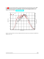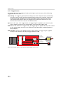
1
User Manual
SM2-D1312-TI6455 / VisionCam PS
CMOS DSP Camera
MAN060 05/2013 V1.0
All information provided in this manual is believed to be accurate and reliable. No
responsibility is assumed by Photonfocus AG for its use. Photonfocus AG reserves the right to
make changes to this information without notice.
Reproduction of this manual in whole or in part, by any means, is prohibited without prior
permission having been obtained from Photonfocus AG.
1
2
Contents
1 Preface
1.1 About Photonfocus
1.2 Contact . . . . . . .
1.3 Sales Offices . . . .
1.4 Further information
1.5 Legend . . . . . . .
.
.
.
.
.
.
.
.
.
.
.
.
.
.
.
.
.
.
.
.
.
.
.
.
.
.
.
.
.
.
.
.
.
.
.
.
.
.
.
.
.
.
.
.
.
.
.
.
.
.
.
.
.
.
.
.
.
.
.
.
.
.
.
.
.
.
.
.
.
.
.
.
.
.
.
.
.
.
.
.
.
.
.
.
.
.
.
.
.
.
.
.
.
.
.
.
.
.
.
.
.
.
.
.
.
.
.
.
.
.
7
7
7
7
7
8
2 How to get started (SM2)
2.1 Introduction . . . . . . . . . . . . . . . . . . . . .
2.2 Get the camera and its accessories . . . . . . . .
2.2.1 SM2-Camera only . . . . . . . . . . . . . .
2.2.2 SM2 Starter Kit . . . . . . . . . . . . . . .
2.2.3 Accessories . . . . . . . . . . . . . . . . . .
2.3 Hardware Installation . . . . . . . . . . . . . . . .
2.4 Software Installation . . . . . . . . . . . . . . . .
2.5 Emulator, Debugger Installation . . . . . . . . .
2.5.1 Code Composer Studio (CCS) . . . . . . .
2.5.2 Emulator . . . . . . . . . . . . . . . . . . .
2.5.3 Connect camera to JTAG . . . . . . . . . .
2.5.4 Framework and examples . . . . . . . . .
2.5.5 Documentation of the code and libraries
2.5.6 microSD card . . . . . . . . . . . . . . . . .
.
.
.
.
.
.
.
.
.
.
.
.
.
.
.
.
.
.
.
.
.
.
.
.
.
.
.
.
.
.
.
.
.
.
.
.
.
.
.
.
.
.
.
.
.
.
.
.
.
.
.
.
.
.
.
.
.
.
.
.
.
.
.
.
.
.
.
.
.
.
.
.
.
.
.
.
.
.
.
.
.
.
.
.
.
.
.
.
.
.
.
.
.
.
.
.
.
.
.
.
.
.
.
.
.
.
.
.
.
.
.
.
.
.
.
.
.
.
.
.
.
.
.
.
.
.
.
.
.
.
.
.
.
.
.
.
.
.
.
.
.
.
.
.
.
.
.
.
.
.
.
.
.
.
.
.
.
.
.
.
.
.
.
.
.
.
.
.
.
.
.
.
.
.
.
.
.
.
.
.
.
.
.
.
.
.
.
.
.
.
.
.
.
.
.
.
.
.
.
.
.
.
.
.
.
.
.
.
.
.
.
.
.
.
.
.
.
.
.
.
.
.
.
.
.
.
.
.
.
.
.
.
.
.
.
.
.
.
.
.
.
.
.
.
.
.
.
.
.
.
.
.
.
.
.
.
.
.
.
.
.
.
.
.
.
.
.
.
.
.
.
.
.
.
.
.
.
.
.
.
.
.
.
.
.
.
.
.
.
.
.
.
.
.
9
9
9
9
10
10
12
14
15
15
15
16
16
16
16
3 Product Specification
3.1 Introduction . . . . . .
3.2 Hardware Overview . .
3.3 Feature Overview . . .
3.4 Technical Specification
.
.
.
.
.
.
.
.
.
.
.
.
.
.
.
.
.
.
.
.
.
.
.
.
.
.
.
.
.
.
.
.
.
.
.
.
.
.
.
.
.
.
.
.
.
.
.
.
.
.
.
.
.
.
.
.
.
.
.
.
.
.
.
.
.
.
.
.
.
.
.
.
.
.
.
.
.
.
.
.
.
.
.
.
.
.
.
.
.
.
.
.
.
.
.
.
.
.
.
.
.
.
.
.
.
.
.
.
.
.
.
.
.
.
.
.
.
.
.
.
.
.
.
.
.
.
.
.
.
.
.
.
.
.
.
.
.
.
.
.
.
.
.
.
.
.
.
.
.
.
.
.
.
.
.
.
.
.
.
.
.
.
.
.
.
.
.
.
.
.
.
.
17
17
18
20
21
4 Functionality
4.1 Image Acquisition . . . . . . . . . . . . . . . . .
4.1.1 Readout Modes . . . . . . . . . . . . . .
4.1.2 Readout Timing . . . . . . . . . . . . . .
4.1.3 Exposure Control . . . . . . . . . . . . .
4.1.4 Maximum Frame Rate . . . . . . . . . .
4.2 Pixel Response . . . . . . . . . . . . . . . . . . .
4.2.1 Linear Response . . . . . . . . . . . . . .
4.2.2 LinLog® . . . . . . . . . . . . . . . . . . .
4.3 Reduction of Image Size . . . . . . . . . . . . .
4.3.1 Region of Interest (ROI) . . . . . . . . .
4.3.2 ROI configuration . . . . . . . . . . . . .
4.3.3 Calculation of the maximum frame rate
.
.
.
.
.
.
.
.
.
.
.
.
.
.
.
.
.
.
.
.
.
.
.
.
.
.
.
.
.
.
.
.
.
.
.
.
.
.
.
.
.
.
.
.
.
.
.
.
.
.
.
.
.
.
.
.
.
.
.
.
.
.
.
.
.
.
.
.
.
.
.
.
.
.
.
.
.
.
.
.
.
.
.
.
.
.
.
.
.
.
.
.
.
.
.
.
.
.
.
.
.
.
.
.
.
.
.
.
.
.
.
.
.
.
.
.
.
.
.
.
.
.
.
.
.
.
.
.
.
.
.
.
.
.
.
.
.
.
.
.
.
.
.
.
.
.
.
.
.
.
.
.
.
.
.
.
.
.
.
.
.
.
.
.
.
.
.
.
.
.
.
.
.
.
.
.
.
.
.
.
.
.
.
.
.
.
.
.
.
.
.
.
.
.
.
.
.
.
.
.
.
.
.
.
.
.
.
.
.
.
.
.
.
.
.
.
.
.
.
.
.
.
.
.
.
.
.
.
.
.
.
.
.
.
.
.
.
.
.
.
.
.
.
.
.
.
.
.
.
.
.
.
.
.
.
.
.
.
.
.
.
.
.
.
25
25
25
27
30
30
31
31
31
36
36
39
39
CONTENTS
.
.
.
.
.
.
.
.
.
.
.
.
.
.
.
.
.
.
.
.
.
.
.
.
.
.
.
.
.
.
.
.
.
.
.
.
.
.
.
.
.
.
.
.
.
.
.
.
.
.
.
.
3
CONTENTS
.
.
.
.
.
.
.
.
.
.
.
.
.
.
.
.
.
.
.
.
.
.
.
.
.
.
.
.
.
.
.
.
.
.
.
.
.
.
.
.
.
.
.
.
.
.
.
.
.
.
.
.
.
.
.
.
.
.
.
.
.
.
.
.
.
.
.
.
.
.
.
.
.
.
.
.
.
.
.
.
.
.
.
.
.
.
.
.
.
.
.
.
.
.
.
.
.
.
.
.
.
.
.
.
.
.
.
.
.
.
.
.
.
.
.
.
.
.
.
.
.
.
.
.
.
.
.
.
.
.
.
.
.
.
.
.
.
.
.
.
.
.
.
.
.
.
.
.
.
.
.
.
.
.
.
.
.
.
.
.
.
.
.
.
.
.
.
.
.
.
.
.
.
.
.
.
.
.
.
.
.
.
.
.
.
.
.
.
.
.
.
.
.
.
.
.
.
.
.
.
.
.
.
.
.
.
.
.
.
.
.
.
.
.
.
.
.
.
.
.
.
.
.
.
.
.
.
.
.
.
.
.
.
.
.
.
.
.
.
.
.
.
.
.
.
.
.
.
.
.
.
.
.
.
.
.
.
.
.
.
.
.
.
.
.
.
.
.
.
.
.
.
.
.
.
.
.
.
.
.
.
.
.
.
.
.
.
.
.
.
.
.
.
.
.
.
.
.
.
.
.
.
.
.
.
.
.
.
.
.
.
.
.
.
.
.
.
.
.
.
.
.
.
.
.
.
.
.
.
.
.
.
.
.
.
.
.
.
.
.
.
.
.
.
.
.
.
.
.
.
.
.
.
.
.
.
.
.
.
.
.
.
.
.
.
.
.
.
.
.
.
.
.
.
.
.
.
.
.
.
.
.
.
.
.
.
.
.
.
.
.
.
.
.
.
.
.
.
.
.
.
.
.
.
.
.
.
.
.
.
.
.
.
.
.
.
.
.
.
.
.
.
.
.
.
.
.
.
.
.
.
.
.
.
.
.
.
.
.
.
.
.
.
.
.
.
.
.
.
.
.
.
.
.
.
.
.
.
.
.
.
.
.
.
.
.
.
.
.
.
.
.
.
.
.
.
.
.
.
.
.
.
.
.
.
.
.
.
.
.
.
.
.
.
.
.
.
.
.
.
.
.
.
.
.
.
.
.
.
.
.
.
.
.
.
.
.
.
.
.
.
.
.
.
.
.
.
.
.
.
.
.
.
.
.
.
.
.
.
.
.
.
.
.
.
.
.
.
.
.
.
.
.
.
.
.
.
.
.
.
.
.
.
.
.
.
.
.
.
.
.
.
.
.
.
.
.
.
.
.
.
.
.
.
.
.
.
.
.
.
.
.
.
.
.
.
.
.
.
.
.
.
.
.
.
.
.
.
.
.
.
.
.
.
.
.
.
.
.
.
.
.
.
.
.
.
.
.
.
.
.
.
.
.
.
.
.
.
.
.
.
.
.
.
.
.
.
.
.
.
.
.
.
.
.
.
.
.
.
.
.
.
.
.
.
.
.
.
.
.
.
.
.
.
.
.
.
.
.
.
.
.
.
.
.
.
.
.
.
.
.
.
.
.
.
.
.
.
.
.
.
.
.
.
.
.
.
.
.
.
.
.
.
.
.
.
.
.
.
.
.
.
.
.
.
.
.
.
.
.
.
.
.
.
.
41
44
47
47
48
49
51
51
55
55
56
57
57
57
59
60
62
62
62
64
65
65
68
68
68
68
71
71
73
73
73
75
75
75
75
5 Hardware Interface
5.1 GigE Connector . . . . . . . . . . . . . . . . . . . .
5.2 Power Supply Connector . . . . . . . . . . . . . . .
5.3 Trigger Connector . . . . . . . . . . . . . . . . . . .
5.4 Status Indicator (SM2 cameras) . . . . . . . . . . .
5.5 Power and Ground Connection for SM2 Cameras .
5.6 Trigger and Strobe Signals for SM2 Cameras . . .
5.6.1 Overview . . . . . . . . . . . . . . . . . . . .
5.6.2 Opto-isolated Interface (power connector)
5.6.3 RS422 Interface . . . . . . . . . . . . . . . .
.
.
.
.
.
.
.
.
.
.
.
.
.
.
.
.
.
.
.
.
.
.
.
.
.
.
.
.
.
.
.
.
.
.
.
.
.
.
.
.
.
.
.
.
.
.
.
.
.
.
.
.
.
.
.
.
.
.
.
.
.
.
.
.
.
.
.
.
.
.
.
.
.
.
.
.
.
.
.
.
.
.
.
.
.
.
.
.
.
.
.
.
.
.
.
.
.
.
.
.
.
.
.
.
.
.
.
.
.
.
.
.
.
.
.
.
.
.
.
.
.
.
.
.
.
.
.
.
.
.
.
.
.
.
.
.
.
.
.
.
.
.
.
.
.
.
.
.
.
.
.
.
.
.
.
.
.
.
.
.
.
.
.
.
.
.
.
.
.
.
.
.
.
.
.
.
.
.
.
.
79
79
79
80
80
81
82
82
82
84
6 Framework Functionalities
6.1 Web Server . . . . . . . . . . . . . . . .
6.1.1 Access to the Web Server . . . .
6.1.2 Information about the Camera
6.1.3 Configuration of the Camera .
6.1.4 Sensor . . . . . . . . . . . . . . .
.
.
.
.
.
.
.
.
.
.
.
.
.
.
.
.
.
.
.
.
.
.
.
.
.
.
.
.
.
.
.
.
.
.
.
.
.
.
.
.
.
.
.
.
.
.
.
.
.
.
.
.
.
.
.
.
.
.
.
.
.
.
.
.
.
.
.
.
.
.
.
.
.
.
.
.
.
.
.
.
.
.
.
.
.
.
.
.
.
.
.
.
.
.
.
.
.
.
.
.
85
85
85
86
89
89
4.4
4.5
4.6
4.7
4.8
4.9
4.10
4.11
4.12
4
4.3.4 Multiple Regions of Interest . . . .
4.3.5 Decimation . . . . . . . . . . . . . .
Trigger and Strobe . . . . . . . . . . . . .
4.4.1 Introduction . . . . . . . . . . . . .
4.4.2 Trigger Source . . . . . . . . . . . .
4.4.3 Exposure Time Control . . . . . . .
4.4.4 Trigger Delay . . . . . . . . . . . . .
4.4.5 Burst Trigger . . . . . . . . . . . . .
4.4.6 Software Trigger . . . . . . . . . .
4.4.7 Strobe Output . . . . . . . . . . . .
Data Path Overview . . . . . . . . . . . . .
Image Correction . . . . . . . . . . . . . .
4.6.1 Overview . . . . . . . . . . . . . . .
4.6.2 Offset Correction (FPN, Hot Pixels)
4.6.3 Gain Correction . . . . . . . . . . .
4.6.4 Corrected Image . . . . . . . . . . .
Digital Gain and Offset . . . . . . . . . . .
Grey Level Transformation (LUT) . . . . .
4.8.1 Gain . . . . . . . . . . . . . . . . . .
4.8.2 Gamma . . . . . . . . . . . . . . . .
4.8.3 User-defined Look-up Table . . . .
4.8.4 Region LUT and LUT Enable . . . .
Convolver (monochrome models only) . .
4.9.1 Functionality . . . . . . . . . . . . .
4.9.2 Settings . . . . . . . . . . . . . . . .
4.9.3 Examples . . . . . . . . . . . . . . .
Crosshairs (monochrome models only) . .
4.10.1 Functionality . . . . . . . . . . . . .
Image Information and Status Line . . . .
4.11.1 Counters and Average Value . . .
4.11.2 Status Line . . . . . . . . . . . . . .
Test Images . . . . . . . . . . . . . . . . . .
4.12.1 Ramp . . . . . . . . . . . . . . . . .
4.12.2 LFSR . . . . . . . . . . . . . . . . . .
4.12.3 Troubleshooting using the LFSR . .
.
.
.
.
.
.
.
.
.
.
.
.
.
.
.
.
.
.
.
.
.
.
.
.
.
.
.
.
.
.
.
.
.
.
.
.
.
.
.
.
.
.
.
.
.
.
.
.
.
.
.
.
.
.
.
.
.
.
.
.
.
.
.
.
.
.
.
.
.
.
.
.
.
.
.
.
.
.
.
.
.
.
.
.
.
.
.
.
.
.
.
.
.
.
.
.
.
.
.
.
.
.
.
.
.
.
.
.
.
.
.
.
.
.
.
.
.
.
.
.
.
.
.
.
.
.
.
.
.
.
.
.
.
.
.
.
.
.
.
.
.
.
.
.
.
.
.
.
.
.
.
.
.
.
.
.
.
.
.
.
.
.
.
.
.
.
.
.
.
.
.
.
.
.
.
6.1.5 Camera .
6.1.6 Save Pic .
6.1.7 Tools . .
6.1.8 View Par
6.1.9 App . . .
6.2 FTP Server . . .
.
.
.
.
.
.
.
.
.
.
.
.
.
.
.
.
.
.
.
.
.
.
.
.
.
.
.
.
.
.
.
.
.
.
.
.
.
.
.
.
.
.
.
.
.
.
.
.
.
.
.
.
.
.
.
.
.
.
.
.
.
.
.
.
.
.
.
.
.
.
.
.
.
.
.
.
.
.
.
.
.
.
.
.
.
.
.
.
.
.
.
.
.
.
.
.
.
.
.
.
.
.
.
.
.
.
.
.
.
.
.
.
.
.
.
.
.
.
.
.
.
.
.
.
.
.
.
.
.
.
.
.
.
.
.
.
.
.
.
.
.
.
.
.
.
.
.
.
.
.
.
.
.
.
.
.
.
.
.
.
.
.
.
.
.
.
.
.
.
.
.
.
.
.
.
.
.
.
.
.
.
.
.
.
.
.
.
.
.
.
.
.
.
.
.
.
.
.
.
.
.
.
.
.
.
.
.
.
.
.
.
.
.
.
.
.
.
.
.
.
.
.
.
.
.
.
.
.
.
.
.
.
.
.
. 89
. 104
. 105
. 106
. 107
. 107
7 Mechanical and Optical Considerations
7.1 Mechanical Interface . . . . . . . . .
7.1.1 Cameras with GigE Interface .
7.2 Optical Interface . . . . . . . . . . . .
7.2.1 Cleaning the Sensor . . . . . .
7.3 CE compliance . . . . . . . . . . . . .
.
.
.
.
.
.
.
.
.
.
.
.
.
.
.
.
.
.
.
.
.
.
.
.
.
.
.
.
.
.
.
.
.
.
.
.
.
.
.
.
.
.
.
.
.
.
.
.
.
.
.
.
.
.
.
.
.
.
.
.
.
.
.
.
.
.
.
.
.
.
.
.
.
.
.
.
.
.
.
.
.
.
.
.
.
.
.
.
.
.
.
.
.
.
.
.
.
.
.
.
.
.
.
.
.
.
.
.
.
.
.
.
.
.
.
.
.
.
.
.
.
.
.
.
.
.
.
.
.
.
.
.
.
.
.
109
. 109
. 109
. 110
. 110
. 112
8 Warranty
113
8.1 Warranty Terms . . . . . . . . . . . . . . . . . . . . . . . . . . . . . . . . . . . . . . . . 113
8.2 Warranty Claim . . . . . . . . . . . . . . . . . . . . . . . . . . . . . . . . . . . . . . . . 113
9 References
115
A Pinouts
117
A.1 Power Supply Connector . . . . . . . . . . . . . . . . . . . . . . . . . . . . . . . . . . . 117
A.2 RS422 Trigger and Strobe Interface . . . . . . . . . . . . . . . . . . . . . . . . . . . . . 118
B Revision History
CONTENTS
121
5
CONTENTS
6
1
Preface
1.1
About Photonfocus
The Swiss company Photonfocus is one of the leading specialists in the development of CMOS
image sensors and corresponding industrial cameras for machine vision, security & surveillance
and automotive markets.
Photonfocus is dedicated to making the latest generation of CMOS technology commercially
available. Active Pixel Sensor (APS) and global shutter technologies enable high speed and
high dynamic range (120 dB) applications, while avoiding disadvantages like image lag,
blooming and smear.
Photonfocus has proven that the image quality of modern CMOS sensors is now appropriate
for demanding applications. Photonfocus’ product range is complemented by custom design
solutions in the area of camera electronics and CMOS image sensors.
Photonfocus is ISO 9001 certified. All products are produced with the latest techniques in order
to ensure the highest degree of quality.
1.2
Contact
Photonfocus AG, Bahnhofplatz 10, CH-8853 Lachen SZ, Switzerland
Sales
Phone: +41 55 451 07 45
Email: [email protected]
Support
Phone: +41 55 451 01 37
Email: [email protected]
Table 1.1: Photonfocus Contact
1.3
Sales Offices
Photonfocus products are available through an extensive international distribution network
and through our key account managers. Details of the distributor nearest you and contacts to
our key account managers can be found at www.photonfocus.com.
1.4
Further information
Photonfocus reserves the right to make changes to its products and documentation without notice. Photonfocus products are neither intended nor certified for
use in life support systems or in other critical systems. The use of Photonfocus
products in such applications is prohibited.
Photonfocus is a trademark and LinLog® is a registered trademark of Photonfocus AG. CameraLink® and GigE Vision® are a registered mark of the Automated
Imaging Association. Product and company names mentioned herein are trademarks or trade names of their respective companies.
7
1 Preface
Reproduction of this manual in whole or in part, by any means, is prohibited
without prior permission having been obtained from Photonfocus AG.
Photonfocus can not be held responsible for any technical or typographical errors.
1.5
Legend
In this documentation the reader’s attention is drawn to the following icons:
Important note
Alerts and additional information
Attention, critical warning
✎
8
Notification, user guide
2
How to get started (SM2)
2.1
Introduction
The SM2-D1312(IE)-TI6455 Series / VisionCam PS is an intelligent camera especially designed for
machine vision applications. The camera consists of the CMOS camera head and the embedded
vision computer. These two main components are developed by Photonfocus AG (camera head)
and IMAGO Technologies (vision computer). This document is a guideline for programming
and understanding the SM2-D1312(IE)-TI6455 Series / VisionCam PS.
This guide shows you:
•
How to get the camera and it’s accessories
•
How to install the required hardware
•
How to install the required software
•
How to acquire your first images and how to modify camera settings
2.2
2.2.1
Get the camera and its accessories
SM2-Camera only
An order of the SM2 camera contains the camera body only (no lense).
Figure 2.1: SM2 camera
9
2 How to get started (SM2)
2.2.2
SM2 Starter Kit
An order of the SM2 Starter Kit, contains the following items:
•
SM2 Camera body (no lense).
•
SM2-JTAG connector
Figure 2.2: SM2-JTAG adapter and camera
2.2.3
Accessories
SM2-JTAG Connector
The SM2-JTAG connector is needed to connect the emulator to the DSP of the SM2 camera. The
JTAG interface is behind the "JTAG / SD-CARD" plate. This connector can be ordered from
Photonfocus.
Figure 2.3: SM2-JTAG adapter
10
Power supply
The power supply can be ordered from Photonfocus.
Figure 2.4: SM2 power supply
SM2 Trigger cables
The SM2 trigger cables packages contains two cables:
•
12pol cable for the Hirose power connector.
•
14pol cable for the MDR-14 connector.
Figure 2.5: SM2 trigger cables
.
2.2 Get the camera and its accessories
11
2 How to get started (SM2)
2.3
Hardware Installation
The hardware installation that is required for this guide is described in this section.
The following hardware is required:
•
PC with Microsoft Windows OS (XP, Vista, Windows 7)
•
A Gigabit Ethernet network interface card (NIC) must be installed in the PC.
•
Photonfocus SM2 camera.
•
Suitable power supply for the camera (see in the camera manual for specification) which
can be ordered from your Photonfocus dealership.
•
GigE cable of at least Cat 5E or 6.
Photonfocus SM2 cameras can also be used under Linux.
Do not bend GigE cables too much. Excess stress on the cable results in transmission errors. In robots applications, the stress that is applied to the GigE cable is
especially high due to the fast movement of the robot arm. For such applications,
special drag chain capable cables are available.
The following list describes the connection of the camera to the PC:
1.
Remove the Photonfocus SM2 camera from its packaging. Please make sure the following
items are included with your camera:
•
Power supply connector
•
SM2 camera body
•
IP address (default: 192.168.1.240)
If any items are missing or damaged, please contact your dealership.
2.
Connect the camera to the GigE interface of your PC with a GigE cable of at least Cat 5E or
6.
Figure 2.6: Rear view of the SM2 camera SM2-D1312(IE)-TI6455-80 with power supply and I/O connector,
Ethernet jack (RJ45) and status LED
12
3.
Connect a suitable power supply to the power plug. The pin out of the connector is
shown in the camera manual.
Check the correct supply voltage and polarity! Do not exceed the operating
voltage range of the camera.
A suitable power supply can be ordered from your Photonfocus dealership.
4.
Connect the power supply to the camera (see Fig. 2.6).
.
2.3 Hardware Installation
13
2 How to get started (SM2)
2.4
Software Installation
This section describes the installation of the required software to accomplish the tasks
described in this chapter.
1.
2.
Use the JavaApplet (tcpdisplay.jar) to connect to the camera. There are differnet ways to
get the JavaApplet.
•
If you have already the JavaApplet and you know the camer IP address, doubleclick
the JavaApplet and enter camera IP address.
•
You can find the JavaApplet in the Photonfocus\SM2 folder, when you have installed
PFInstaller and selected the SM2 package during installation.
•
If you don’t know the camera IP address, use the VIBFinder.exe tool (you can find it
also in the Photonfocus\SM2 folder of the PFInstaller installation). Click to "Find
Devices", select the camera and click to "Show Properties". Now you can click to
"Open TCP Display".
•
The JavaApplet (tcpdisplay.jar) is also on the microSD card of the camera. Unplug the
microSD card and connect it to a computer or download the JavaApplet directly over
FTP (ftp://192.168.1.240, username, password)
The web browser displays the web server main window as shown in Fig. 2.7.
Figure 2.7: Framework (web server) start page
.
14
2.5
Emulator, Debugger Installation
This section describes what software and tools are needed to compile own c/c++ code and
download it to the DSP.
2.5.1
Code Composer Studio (CCS)
The Code Composer Studio (CCS) is an integrated development environment (IDE) for Texas
Instruments (TI) embedded processor families. CCS comprises a suite of tools used to develop
and debug embedded applications. It includes compilers for each of TI’s device families, source
code editor, project build environment, debugger, profiler, simulators, real-time operating
system and many other features.
Here are more information about the CCS: www.ti.com/tool/ccstudio.
The Node Locked Single User (N01D) cost about 445US$. There is also a 90day evaluation
version (CSS-FREE) avialable. The evaluation version has no other limitations. More
informations about the licensing of the CSS:
http://processors.wiki.ti.com/index.php/Licensing_-_CCS.
2.5.2
Emulator
For debugging a emulator is needed. Photonfocus recomment the XDS200 for about 295US$.
Pros of the XDS200:
•
No additional driver is needed. The driver is part of the CCS installation.
•
Only a USB connector (no additional power needed), perfect for notebook users!
•
Low cost (XDS560 family is about 1000US$).
The XDS200 can be ordered directly from the Texas Instruments webs site. Find more
information about the XDS200 here: www.ti.com/tool/xds200.
Figure 2.8: XDS200 emulator
2.5 Emulator, Debugger Installation
15
2 How to get started (SM2)
2.5.3
Connect camera to JTAG
Remove the "JTAG / SD-Card" plate, before connecting the JTAG. Figure 2.9 shows how to
connect the SM2-JTAG connector and the XDS200 emulator.
Figure 2.9: How to connect camera to XDS200 emulator
2.5.4
Framework and examples
The framework and the examples are working with the CCS. We provide also the source code
of the framework and the examples.
2.5.5
Documentation of the code and libraries
These documentations are on the microSD card of the SM2 camera.
2.5.6
microSD card
The microSD card of the SM2 camera contains the following:
•
All needed files for CCS development (framework, source code, libraries, examples) in a
zip file
•
Camera manual and source code documentation.
•
VIBFinder.exe, this windows tool finds the SM2 camera in the network, if the user does
not know the camera IP address.
•
tcpdisplay.jar, JavaApplet to connect to camera build-in webserver
•
Ethernet.ini, to change the camera IP-address, default address is: 192.168.1.240
Remove the "JTAG / SD-Card" plate, before accessing the microSD card.
Figure 2.10: microSD card
16
3
Product Specification
3.1
Introduction
The SM2-D1312(IE)-TI6455 CMOS camera series are built around the A1312(IE/C) CMOS image
sensor from Photonfocus and IMAGO Technologies, that provides a resolution of 1312 x 1082
pixels at a wide range of spectral sensitivity. There are standard monochrome and NIR
enhanced monochrome (IE) models. The camera series is aimed at standard applications in
industrial image processing. The principal advantages are:
•
Resolution of 1312 x 1082 pixels.
•
Wide spectral sensitivity from 320 nm to 1030 nm for monochrome models.
•
Enhanced near infrared (NIR) sensitivity with the A1312IE CMOS image sensor.
•
High quantum efficiency: > 50% for monochrome models and between 25% and 45% for
colour models.
•
High pixel fill factor (> 60%).
•
Superior signal-to-noise ratio (SNR).
•
Low power consumption at high speeds.
•
Very high resistance to blooming.
•
High dynamic range of up to 120 dB.
•
Ideal for high speed applications: Global shutter.
•
Image resolution of up to 12 bit.
•
On camera shading correction.
•
3x3 Convolver for image pre-processing included on camera.
•
Up to 512 regions of interest (MROI).
•
2 look-up tables (12-to-8 bit) on user-defined image regions (Region-LUT).
•
Crosshairs overlay on the image (monochrome models only).
•
Image information and camera settings inside the image (status line).
•
Software provided for setting and storage of camera parameters.
•
The camera has a Gigabit Ethernet interface.
•
Texas Instrument TMS320C6455 DSP with 1.2GHz and 9600MIPS
•
512MB onboard DDR RAM.
•
The camera has a Gigabit Ethernet interface.
•
2GB microSD card (max. 32GB).
•
Advanced I/O capabilities: 3 isolated trigger inputs, 3 differential isolated RS-422 inputs, 3
differential isolated RS-422 outputs and 3 isolated outputs.
•
Wide power input range from 12 V (-10 %) to 24V (+10 %).
The general specification and features of the camera are listed in the following sections.
17
3 Product Specification
3.2
Hardware Overview
The three main components in the block diagram are the CMOS camera module, the FPGA and
the digital signal processor. These components are especially designed to transfer high data
rates and to communicate with each other. The used high speed communication protocol is
called Sun-System-Protocol. The CMOS camera module is a D1312(IE) camera module from
Photonfocus, with all its included features like 1312 x 1082 pixel camera resolution, global
shutter, shading correction and LinLog® technology. The image processing computer (FPGA /
DSP / SDRAM / Flash) is a module based on VisionBox technology from IMAGO Technologies.
The function of this module is the handling of the image data, the doing the image processing
and performing the communication between the components and peripheral devices. The
digital signal processor has a fast internal memory of 2048 kB and runs with a maximum
frequency of 1200 MHz. There are up to 512 MB external SDRAM, storing image data and
program data.
18
C M O S
C a m e ra
F P G A
C 6 4 5 5 D S P
1 2 0 0 M H z
R A M
5 1 2 M B
F la s h
4 M B
R S 4 2 2 T r a n s c e iv e r
(3 x In / 3 x O u t)
3 x
3 x O
1 x
2
O p
p t
R S
x L
to In
o O u t
2 3 2
E D
m ic r o S D C a r d
E th e rn e t
1 0 0 0 M b it/s
Figure 3.1: Hardware overview
Each SM2-D1312(IE)-TI6455 / VisionCam PS camera features an internal flash memory of 4
MBytes and a µSD Card. The internal flash memory is used to store the bootloader, some
configuration files and the firmware. The µSD card is used to store image data, the executable
program and other user data. The communication with external devices is realized via a 1000
Mbit/s Ethernet connection. In this way it is possible to perform high data rates. For other
communication purposes, the optocoupled inputs and outputs, the RS422 transceivers and the
serial port are helpful.
3.2 Hardware Overview
19
3 Product Specification
3.3
Feature Overview
Characteristics
SM2-D1312(IE)-TI6455
Interface
Gigabit Ethernet, TCP/IP, FTP µSD card
Camera Control
Web server or programming library
Trigger Modes
Software Trigger / External isolated trigger input / PLC Trigger
Features
Greyscale resolution 12 bit / 10 bit / 8 bit
Region of Interest (ROI)
Test pattern (LFSR and grey level ramp)
Shading Correction (Offset and Gain)
3x3 Convolver included on camera
High blooming resistance
isolated trigger input and isolated strobe output
2 look-up tables (12-to-8 bit) on user-defined image region (Region-LUT)
Up to 512 regions of interest (MROI)
Image information and camera settings inside the image (status line)
Crosshairs overlay on the image
Table 3.1: Feature overview (see Chapter 4 for more information)
Figure 3.2: SM2-D1312(IE)-TI6455 CMOS camera with C-mount lens
20
3.4
Technical Specification
Technical Parameters
SM2-D1312(IE)-TI6455
Technology
CMOS active pixel (APS)
Scanning system
Progressive scan
Optical format / diagonal
1” (13.6 mm diagonal) @ maximum
resolution
2/3” (11.6 mm diagonal) @ 1024 x 1024
resolution
Resolution
1312 x 1082 pixels
Pixel size
8 µm x 8 µm
Active optical area
10.48 mm x 8.64 mm (maximum)
Random noise
< 0.3 DN @ 8 bit 1)
Fixed pattern noise (FPN)
3.4 DN @ 8 bit / correction OFF 1)
Fixed pattern noise (FPN)
< 1DN @ 8 bit / correction ON 1)2)
Dark current SM2-D1312-TI6455
0.65 fA / pixel @ 27 °C
Dark current SM2-D1312IE-TI6455
0.79 fA / pixel @ 27 °C
Full well capacity
~ 90 ke−
Spectral range SM2-D1312-TI6455
350 nm ... 980 nm (see Fig. 3.3)
Spectral range SM21-D1312IE-TI6455
320 nm ... 1000 nm (see Fig. 3.4)
Responsivity MV1-D1312 and DR1-D1312
295 x103 DN/(J/m2 ) @ 670 nm / 8 bit
Responsivity MV1-D1312IE and DR1-D1312IE
305 x103 DN/(J/m2 ) @ 870 nm / 8 bit
Quantum Efficiency
> 50 %
Optical fill factor
> 60 %
Dynamic range
60 dB in linear mode, 120 dB with LinLog®
Colour format (colour models)
RGB Bayer Raw Data Pattern
Characteristic curve
Linear, LinLog®
Shutter mode
Global shutter
Greyscale resolution
12 bit / 10 bit / 8 bit
Table 3.2: General specification of the SM2-D1312(IE)-TI6455 camera series (Footnotes:
are typical values. 2) Indicated values are subject to confirmation.
3.4 Technical Specification
1)
Indicated values
21
3 Product Specification
SM2-D1312(IE)-TI6455-80
SM2-D1312(IE)-TI6455-160
10 µs ... 0.83 s
10 µs ... 0.42 s
50 ns
25 ns
54 fps
108 fps
40 MHz
80 MHz
25 ns
12.5 ns
1
2
Exposure Time
Exposure time increment
5)
Frame rate
( Tint = 10 µs)
Pixel clock frequency
Pixel clock cycle
Camera taps
Read out mode
sequential or simultaneous
Table 3.3: Model-specific parameters (Footnotes:
5)
Maximum frame rate @ full resolution @ 8 bit).
SM2-D1312(IE)-TI6455-80
Operating temperature / moisture
Storage temperature / moisture
SM2-D1312(IE)-TI6455-160
0°C ... 50°C / 20 ... 80 %
-25°C ... 60°C / 20 ... 95 %
Camera power supply
+12 V DC (± 10 %)
Trigger signal input range
+12 .. +24 V DC
Strobe signal power supply
+12 .. +24 V DC
Strobe signal sink current (average)
Max. power consumption @ 12 V
max. 8 mA
< TBD W
< TBD W
Lens mount
C-Mount (CS-Mount optional)
Dimensions
60 x 60 x TBD mm3
Mass
Conformity
600 g
CE / RoHS / WEE
Table 3.4: Physical characteristics and operating ranges of the SM2-D1312(IE)-TI6455 camera series
.
22
Fig. 3.3 shows the quantum efficiency and the responsivity of the monochrome A1312 CMOS
sensor, displayed as a function of wavelength. For more information on photometric and
radiometric measurements see the Photonfocus application note AN008 available in the
support area of our website www.photonfocus.com.
60%
QE
1200
Responsivity
50%
1000
800
30%
600
20%
Responsivity [V
V/J/m²]
Quantum
m Efficiency
40%
400
10%
200
0%
200
0
300
400
500
600
700
800
900
1000
1100
Wavelength [nm]
Figure 3.3: Spectral response of the A1312 CMOS monochrome image sensor (standard) in the SM2-D1312TI6455 camera series
3.4 Technical Specification
23
3 Product Specification
Fig. 3.4 shows the quantum efficiency and the responsivity of the monochrome A1312IE CMOS
sensor, displayed as a function of wavelength. The enhancement in the NIR quantum efficiency
could be used to realize applications in the 900 to 1064 nm region.
60%
1200
QE [%]
1000
40%
800
30%
600
20%
400
10%
200
0%
300
Responsivity [V/J/m^2]
Quantum Efficiency
Responsivity [V/W/m^2]
50%
0
400
500
600
700
800
900
1000
1100
Wavelength [nm]
Figure 3.4: Spectral response of the A1312IE monochrome image sensor (NIR enhanced) in the SM2D1312IE-TI6455 camera series
24
4
Functionality
This chapter serves as an overview of the camera configuration modes and explains camera
features. The goal is to describe what can be done with the camera. The setup of the
SM2-D1312(IE)-TI6455 series cameras is explained in later chapters.
4.1
4.1.1
Image Acquisition
Readout Modes
The SM2-D1312(IE)-TI6455 cameras provide two different readout modes:
Sequential readout Frame time is the sum of exposure time and readout time. Exposure time
of the next image can only start if the readout time of the current image is finished.
Simultaneous readout (interleave) The frame time is determined by the maximum of the
exposure time or of the readout time, which ever of both is the longer one. Exposure
time of the next image can start during the readout time of the current image.
Readout Mode
SM2-D1312(IE)-TI6455 Series
Sequential readout
available
Simultaneous readout
available
Table 4.1: Readout mode of SM2-D1312(IE)-TI6455Series camera
The following figure illustrates the effect on the frame rate when using either the sequential
readout mode or the simultaneous readout mode (interleave exposure).
fp s = 1 /r e a d o u t tim e
F ra m e ra te
(fp s)
S im u lta n e o u s
re a d o u t m o d e
fp s = 1 /e x p o s u r e tim e
S e q u e n tia l
re a d o u t m o d e
fp s = 1 /( r e a d o u t tim e + e x p o s u r e tim e )
e x p o s u re tim e < re a d o u t tim e
e x p o s u re tim e = re a d o u t tim e
e x p o s u re tim e > re a d o u t tim e
E x p o s u re tim e
Figure 4.1: Frame rate in sequential readout mode and simultaneous readout mode
Sequential readout mode For the calculation of the frame rate only a single formula applies:
frames per second equal to the inverse of the sum of exposure time and readout time.
25
4 Functionality
Simultaneous readout mode (exposure time < readout time) The frame rate is given by the
readout time. Frames per second equal to the inverse of the readout time.
Simultaneous readout mode (exposure time > readout time) The frame rate is given by the
exposure time. Frames per second equal to the inverse of the exposure time.
The simultaneous readout mode allows higher frame rates. However, if the exposure time
greatly exceeds the readout time, then the effect on the frame rate is neglectable.
In simultaneous readout mode image output faces minor limitations. The overall
linear sensor reponse is partially restricted in the lower grey scale region.
When changing readout mode from sequential to simultaneous readout mode
or vice versa, new settings of the BlackLevelOffset and of the image correction
are required.
Sequential readout
By default the camera continuously delivers images as fast as possible ("Free-running mode")
in the sequential readout mode. Exposure time of the next image can only start if the readout
time of the current image is finished.
e x p o s u re
re a d o u t
e x p o s u re
re a d o u t
Figure 4.2: Timing in free-running sequential readout mode
When the acquisition of an image needs to be synchronised to an external event, an external
trigger can be used (refer to Section 4.4). In this mode, the camera is idle until it gets a signal
to capture an image.
e x p o s u re
re a d o u t
id le
e x p o s u re
e x te r n a l tr ig g e r
Figure 4.3: Timing in triggered sequential readout mode
Simultaneous readout (interleave exposure)
To achieve highest possible frame rates, the camera must be set to "Free-running mode" with
simultaneous readout. The camera continuously delivers images as fast as possible. Exposure
time of the next image can start during the readout time of the current image.
e x p o s u re n
re a d o u t n -1
id le
e x p o s u re n + 1
re a d o u t n
id le
re a d o u t n + 1
fr a m e tim e
Figure 4.4: Timing in free-running simultaneous readout mode (readout time> exposure time)
26
e x p o s u re n -1
id le
e x p o s u re n + 1
e x p o s u re n
re a d o u t n -1
id le
re a d o u t n
fr a m e tim e
Figure 4.5: Timing in free-running simultaneous readout mode (readout time< exposure time)
When the acquisition of an image needs to be synchronised to an external event, an external
trigger can be used (refer to Section 4.4). In this mode, the camera is idle until it gets a signal
to capture an image.
Figure 4.6: Timing in triggered simultaneous readout mode
4.1.2
Readout Timing
Sequential readout timing
By default, the camera is in free running mode and delivers images without any external
control signals. The sensor is operated in sequential readout mode, which means that the
sensor is read out after the exposure time. Then the sensor is reset, a new exposure starts and
the readout of the image information begins again. The data is output on the rising edge of
the pixel clock. The signals FRAME_VALID (FVAL) and LINE_VALID (LVAL) mask valid image
information. The signal SHUTTER indicates the active exposure period of the sensor and is shown
for clarity only.
Simultaneous readout timing
To achieve highest possible frame rates, the camera must be set to "Free-running mode" with
simultaneous readout. The camera continuously delivers images as fast as possible. Exposure
time of the next image can start during the readout time of the current image. The data is
output on the rising edge of the pixel clock. The signals FRAME_VALID (FVAL) and LINE_VALID (LVAL)
mask valid image information. The signal SHUTTER indicates the active integration phase of the
sensor and is shown for clarity only.
4.1 Image Acquisition
27
4 Functionality
P C L K
F r a m e T im e
S H U T T E R
E x p o s u re
T im e
F V A L
C P R E
L in e p a u s e
L in e p a u s e
L in e p a u s e
L V A L
F ir s t L in e
D V A L
D A T A
Figure 4.7: Timing diagram of sequential readout mode
28
L a s t L in e
P C L K
F r a m e T im e
S H U T T E R
E x p o s u re
T im e
E x p o s u re
T im e
F V A L
C P R E
L in e p a u s e
L in e p a u s e
L in e p a u s e
C P R E
L V A L
F ir s t L in e
L a s t L in e
D V A L
D A T A
Figure 4.8: Timing diagram of simultaneous readout mode (readout time > exposure time)
P C L K
F r a m e T im e
S H U T T E R
E x p o s u r e T im e
F V A L
C P R E
L in e p a u s e
L in e p a u s e
L in e p a u s e
C P R E
L V A L
F ir s t L in e
L a s t L in e
D V A L
D A T A
Figure 4.9: Timing diagram simultaneous readout mode (readout time < exposure time)
4.1 Image Acquisition
29
4 Functionality
Frame time
Frame time is the inverse of the frame rate.
Exposure time
Period during which the pixels are integrating the incoming light.
PCLK
Pixel clock on internal camera interface.
SHUTTER
Internal signal, shown only for clarity. Is ’high’ during the exposure
time.
FVAL (Frame Valid)
Is ’high’ while the data of one complete frame are transferred.
LVAL (Line Valid)
Is ’high’ while the data of one line are transferred. Example: To transfer
an image with 640x480 pixels, there are 480 LVAL within one FVAL active
high period. One LVAL lasts 640 pixel clock cycles.
DVAL (Data Valid)
Is ’high’ while data are valid.
DATA
Transferred pixel values. Example: For a 100x100 pixel image, there are
100 values transferred within one LVAL active high period, or 100*100
values within one FVAL period.
Line pause
Delay before the first line and after every following line when reading
out the image data.
Table 4.2: Explanation of control and data signals used in the timing diagram
These terms will be used also in the timing diagrams of Section 4.4.
4.1.3
Exposure Control
The exposure time defines the period during which the image sensor integrates the incoming
light. Refer to Section 3.4 for the allowed exposure time range.
4.1.4
Maximum Frame Rate
The maximum frame rate depends on the exposure time and the size of the image (see Section
4.3.)
The maximal frame rate with current camera settings can be read out from the
property FrameRateMax (AcquisitionFrameRateMax in GigE cameras).
.
30
4.2
4.2.1
Pixel Response
Linear Response
The camera offers a linear response between input light signal and output grey level. This can
be modified by the use of LinLog® as described in the following sections. In addition, a linear
digital gain may be applied, as follows. Please see Table 3.2 for more model-dependent
information.
Black Level Adjustment
The black level is the average image value at no light intensity. It can be adjusted by the
software. Thus, the overall image gets brighter or darker. Use a histogram to control the
settings of the black level.
In CameraLink® cameras the black level is called "BlackLevelOffset" and in GigE
cameras "BlackLevel".
4.2.2
LinLog®
Overview
The LinLog® technology from Photonfocus allows a logarithmic compression of high light
intensities inside the pixel. In contrast to the classical non-integrating logarithmic pixel, the
LinLog® pixel is an integrating pixel with global shutter and the possibility to control the
transition between linear and logarithmic mode.
In situations involving high intrascene contrast, a compression of the upper grey level region
can be achieved with the LinLog® technology. At low intensities each pixel shows a linear
response. At high intensities the response changes to logarithmic compression (see Fig. 4.10).
The transition region between linear and logarithmic response can be smoothly adjusted by
software and is continuously differentiable and monotonic.
G re y
V a lu e
S a tu r a tio n
1 0 0 %
L in e a r
R e s p o n s e
W e a k c o m p r e s s io n
R e s u ltin g L in lo g
R e s p o n s e
S tr o n g c o m p r e s s io n
0 %
V a lu e 1
V a lu e 2
L ig h t In te n s ity
Figure 4.10: Resulting LinLog2 response curve
4.2 Pixel Response
31
4 Functionality
LinLog® is controlled by up to 4 parameters (Time1, Time2, Value1 and Value2). Value1 and Value2
correspond to the LinLog® voltage that is applied to the sensor. The higher the parameters
Value1 and Value2 respectively, the stronger the compression for the high light intensities. Time1
and Time2 are normalised to the exposure time. They can be set to a maximum value of 1000,
which corresponds to the exposure time.
Examples in the following sections illustrate the LinLog® feature.
LinLog1
In the simplest way the pixels are operated with a constant LinLog® voltage which defines the
knee point of the transition.This procedure has the drawback that the linear response curve
changes directly to a logarithmic curve leading to a poor grey resolution in the logarithmic
region (see Fig. 4.12).
V
L in L o g
t
e x p
V a lu e 1
= V a lu e 2
T im e 1 = T im e 2 = m a x .
= 1 0 0 0
0
t
Figure 4.11: Constant LinLog voltage in the Linlog1 mode
Typical LinLog1 Response Curve − Varying Parameter Value1
Time1=1000, Time2=1000, Value2=Value1
300
Output grey level (8 bit) [DN]
250
V1 = 15
V1 = 16
V1 = 17
200
V1 = 18
V1 = 19
150
100
50
0
Illumination Intensity
Figure 4.12: Response curve for different LinLog settings in LinLog1 mode
.
32
LinLog2
To get more grey resolution in the LinLog® mode, the LinLog2 procedure was developed. In
LinLog2 mode a switching between two different logarithmic compressions occurs during the
exposure time (see Fig. 4.13). The exposure starts with strong compression with a high
LinLog® voltage (Value1). At Time1 the LinLog® voltage is switched to a lower voltage resulting in
a weaker compression. This procedure gives a LinLog® response curve with more grey
resolution. Fig. 4.14 and Fig. 4.15 show how the response curve is controlled by the three
parameters Value1, Value2 and the LinLog® time Time1.
Settings in LinLog2 mode, enable a fine tuning of the slope in the logarithmic
region.
V
L in L o g
t
e x p
V a lu e 1
V a lu e 2
T im e 1
0
T im e 1
T im e 2 = m a x .
= 1 0 0 0
t
Figure 4.13: Voltage switching in the Linlog2 mode
Typical LinLog2 Response Curve − Varying Parameter Time1
Time2=1000, Value1=19, Value2=14
300
T1 = 840
Output grey level (8 bit) [DN]
250
T1 = 920
T1 = 960
200
T1 = 980
T1 = 999
150
100
50
0
Illumination Intensity
Figure 4.14: Response curve for different LinLog settings in LinLog2 mode
4.2 Pixel Response
33
4 Functionality
Typical LinLog2 Response Curve − Varying Parameter Time1
Time2=1000, Value1=19, Value2=18
200
Output grey level (8 bit) [DN]
180
160
140
120
T1 = 880
T1 = 900
T1 = 920
T1 = 940
T1 = 960
T1 = 980
T1 = 1000
100
80
60
40
20
0
Illumination Intensity
Figure 4.15: Response curve for different LinLog settings in LinLog2 mode
LinLog3
To enable more flexibility the LinLog3 mode with 4 parameters was introduced. Fig. 4.16 shows
the timing diagram for the LinLog3 mode and the control parameters.
V
L in L o g
t
e x p
V a lu e 1
V a lu e 2
T im e 1
V a lu e 3 = C o n s ta n t = 0
T im e 2
T im e 1
Figure 4.16: Voltage switching in the LinLog3 mode
.
34
T im e 2
t
t
e x p
Typical LinLog2 Response Curve − Varying Parameter Time2
Time1=850, Value1=19, Value2=18
300
T2 = 950
T2 = 960
T2 = 970
T2 = 980
T2 = 990
Output grey level (8 bit) [DN]
250
200
150
100
50
0
Illumination Intensity
Figure 4.17: Response curve for different LinLog settings in LinLog3 mode
4.2 Pixel Response
35
4 Functionality
4.3
Reduction of Image Size
With Photonfocus cameras there are several possibilities to focus on the interesting parts of an
image, thus reducing the data rate and increasing the frame rate. The most commonly used
feature is Region of Interest (ROI).
4.3.1
Region of Interest (ROI)
Some applications do not need full image resolution (e.g. 1312 x 1082 pixels). By reducing the
image size to a certain region of interest (ROI), the frame rate can be increased. A region of
interest can be almost any rectangular window and is specified by its position within the full
frame and its width (W) and height (H). Fig. 4.18 and Fig. 4.19 how possible configurations for
the region of interest, and Table 4.3 present numerical examples of how the frame rate can be
increased by reducing the ROI.
Both reductions in x- and y-direction result in a higher frame rate.
The minimum width of the region of interest depends on the model of the MV1D1312(I) camera series. For more details please consult Table 4.4 and Table 4.5.
The minimum width must be positioned symmetrically towards the vertical center line of the sensor as shown in Fig. 4.18 and Fig. 4.19). A list of possible
settings of the ROI for each camera model is given in Table 4.5.
³ 2 0 8 P ix e l
³ 2 0 8 P ix e l + m o d u lo 3 2 P ix e l
³ 2 0 8 P ix e l
³ 2 0 8 P ix e l
+ m o d u lo 3 2 P ix e l
a )
b )
Figure 4.18: Possible configuration of the region of interest with SM2-D1312(IE)-TI6455-80 CMOS camera
✎
36
It is recommended to re-adjust the settings of the shading correction each time
a new region of interest is selected.
³ 2 7 2 p ix e l
³ 2 7 2 p ix e l + m o d u lo 3 2 p ix e l
³ 2 7 2 p ix e l
³ 2 7 2 p ix e l
+ m o d u lo 3 2 p ix e l
b )
a )
Figure 4.19: Possible configuration of the region of interest with SM2-D1312(IE)-TI6455-160 CMOS camera
Any region of interest may NOT be placed outside of the center of the sensor. Examples shown
in Fig. 4.20 illustrate configurations of the ROI that are NOT allowed.
a )
b )
Figure 4.20: ROI configuration examples that are NOT allowed
4.3 Reduction of Image Size
37
4 Functionality
ROI Dimension [Standard]
SM2-D1312(IE)-TI6455-80
SM2-D1312(IE)-TI6455-160
1312 x 1082 (full resolution)
54 fps
108 fps
1248 x 1082
56 fps
113 fps
1280 x 1024 (SXGA)
58 fps
117 fps
1280 x 768 (WXGA)
78 fps
156 fps
800 x 600 (SVGA)
157 fps
310 fps
640 x 480 (VGA)
241 fps
472 fps
288 x 1
not allowed ROI setting
not allowed ROI setting
480 x 1
10593 fps
not allowed ROI setting
544 x 1
10498 fps
11022 fps
544 x 1082
125 fps
249 fps
480 x 1082
141 fps
not allowed ROI setting
1312 x 544
107 fps
214 fps
1248 x 544
112 fps
224 fps
1312 x 256
227 fps
445 fps
1248 x 256
238 fps
466 fps
544 x 544
248 fps
485 fps
480 x 480
314 fps
not allowed ROI setting
1024 x 1024
72 fps
145 fps
1056 x 1056
68 fps
136 fps
1312 x 1
9541 fps
10460 fps
1248 x 1
9615 fps
10504 fps
Table 4.3: Frame rates of different ROI settings (exposure time 10 µs; correction on, and sequential readout
mode).
38
.
4.3.2
ROI configuration
In the SM2-D1312(IE)-TI6455 camera series the following two restrictions have to be respected
for the ROI configuration:
•
The minimum width (w) of the ROI is camera model dependent, consisting of 416 pixel in
the SM2-D1312(IE)-TI6455-80 camera, of 544 pixel in the SM2-D1312(IE)-TI6455-160
camera.
•
The region of interest must overlap a minimum number of pixels centered to the left and
to the right of the vertical middle line of the sensor (ovl).
For any camera model of the SM2-D1312(IE)-TI6455 camera series the allowed ranges for the
ROI settings can be deduced by the following formula:
xmin = max(0, 656 + ovl − w)
xmax = min(656 − ovl, 1312 − w)
.
where "ovl" is the overlap over the middle line and "w" is the width of the region of interest.
Any ROI settings in x-direction exceeding the minimum ROI width must be modulo 32.
ROI width (w)
overlap (ovl)
width condition
SM2-D1312(IE)-TI6455-80
SM2-D1312(IE)-TI6455-160
416 ... 1312
544 ... 1312
208
272
modulo 32
modulo 32
Table 4.4: Summary of the ROI configuration restrictions for the SM2-D1312(IE)-TI6455 camera series indicating the minimum ROI width (w) and the required number of pixel overlap (ovl) over the sensor middle
line
The settings of the region of interest in x-direction are restricted to modulo 32
(see Table 4.5).
There are no restrictions for the settings of the region of interest in y-direction.
4.3.3
Calculation of the maximum frame rate
The frame rate mainly depends on the exposure time and readout time. The frame rate is the
inverse of the frame time.
1
fps = tframe
Calculation of the frame time (sequential mode)
4.3 Reduction of Image Size
39
4 Functionality
Width
ROI-X (SM2-D1312(IE)-TI6455-80)
ROI-X (SM2-D1312(IE)-TI6455-160)
288
not available
not available
320
not available
not available
352
not available
not available
384
not available
not available
416
448
not available
448
416 ... 448
not available
480
384 ... 448
not available
512
352 ... 448
not available
544
320 ... 448
384
576
288 ... 448
352 ... 384
608
256 ... 448
320 ... 352
640
224 ... 448
288 ... 384
672
192 ... 448
256 ... 384
704
160 ... 448
224 ... 384
736
128 ... 448
192 ... 384
768
96 ... 448
160 ... 384
800
64 ... 448
128 ... 384
832
32 ... 448
96 ... 384
864
0 ... 448
64 ... 384
896
0 ... 416
32 ... 384
...
...
...
1248
0 ... 64
0 ... 64
1312
0
0
Table 4.5: Some possible ROI-X settings (SM2-D1312(IE)-TI6455 series)
tframe ≥ texp + tro
Typical values of the readout time tro are given in table Table 4.6. Calculation of the frame time
(simultaneous mode)
The calculation of the frame time in simultaneous read out mode requires more detailed data
input and is skipped here for the purpose of clarity.
A frame rate calculator for calculating the maximum frame rate is available in
the support area of the Photonfocus website.
An overview of resulting frame rates in different exposure time settings is given in table Table
4.7.
40
ROI Dimension
SM2-D1312(IE)-TI6455-80
SM2-D1312(IE)-TI6455-160
1312 x 1082
tro = 18.23 ms
tro = 9.12 ms
1248 x 1082
tro = 17.37 ms
tro = 8.68 ms
1024 x 512
tro = 6.78 ms
tro = 3.39 ms
1056 x 512
tro = 6.99 ms
tro = 3.49 ms
1024 x 256
tro = 3.39 ms
tro = 1.70 ms
1056 x 256
tro = 3.49 ms
tro = 1.75 ms
Table 4.6: Read out time at different ROI settings for the SM2-D1312(IE)-TI6455 CMOS camera series in
sequential read out mode.
Exposure time
SM2-D1312(IE)-TI6455-80
SM2-D1312(IE)-TI6455-160
10 µs
54 / 54 fps
108 / 108 fps
100 µs
54 / 54 fps
107 / 108 fps
500 µs
53 / 54 fps
103 / 108 fps
1 ms
51 / 54 fps
98 / 108 fps
2 ms
49 / 54 fps
89 / 108 fps
5 ms
42 / 54 fps
70 / 108 fps
10 ms
35 / 54 fps
52 / 99 fps
12 ms
33 / 54 fps
47 / 82 fps
Table 4.7: Frame rates of different exposure times, [sequential readout mode / simultaneous readout mode
], resolution 1312 x 1082 pixel, FPN correction on.
4.3.4
Multiple Regions of Interest
The SM2-D1312(IE)-TI6455 camera series can handle up to 512 different regions of interest. This
feature can be used to reduce the image data and increase the frame rate. An application
example for using multiple regions of interest (MROI) is a laser triangulation system with
several laser lines. The multiple ROIs are joined together and form a single image, which is
transferred to the frame grabber.
An individual MROI region is defined by its starting value in y-direction and its height. The
starting value in horizontal direction and the width is the same for all MROI regions and is
defined by the ROI settings. The maximum frame rate in MROI mode depends on the number
of rows and columns being read out. Overlapping ROIs are allowed. See Section 4.3.3 for
information on the calculation of the maximum frame rate.
Fig. 4.21 compares ROI and MROI: the setups (visualized on the image sensor area) are
displayed in the upper half of the drawing. The lower half shows the dimensions of the
resulting image. On the left-hand side an example of ROI is shown and on the right-hand side
an example of MROI. It can be readily seen that resulting image with MROI is smaller than the
resulting image with ROI only and the former will result in an increase in image frame rate.
Fig. 4.22 shows another MROI drawing illustrating the effect of MROI on the image content.
Fig. 4.23 shows an example from hyperspectral imaging where the presence of spectral lines at
known regions need to be inspected. By using MROI only a 656x54 region need to be readout
and a frame rate of 4300 fps can be achieved. Without using MROI the resulting frame rate
would be 216 fps for a 656x1082 ROI.
.
4.3 Reduction of Image Size
41
4 Functionality
(0 , 0 )
(0 , 0 )
M R O I 0
R O I
M R O I 1
M R O I 2
(1 3 1 1 , 1 0 8 1 )
(1 3 1 1 , 1 0 8 1 )
M R O I 0
M R O I 1
R O I
Figure 4.21: Multiple Regions of Interest
Figure 4.22: Multiple Regions of Interest with 5 ROIs
42
M R O I 2
6 5 6 p ix e l
(0 , 0 )
1 p ix e l
2 p ix e l
1 p ix e l
2 0 p ix e l
2 p ix e l
2 6 p ix e l
2 p ix e l
C h e m ic a l A g e n t
A
B
C
(1 3 1 1 , 1 0 8 1 )
Figure 4.23: Multiple Regions of Interest in hyperspectral imaging
4.3 Reduction of Image Size
43
4 Functionality
4.3.5
Decimation
Decimation reduces the number of pixels in y-direction. Decimation can also be used together
with ROI or MROI. Decimation in y-direction transfers every nth row only and directly results in
reduced read-out time and higher frame rate respectively.
Fig. 4.24 shows decimation on the full image. The rows that will be read out are marked by red
lines. Row 0 is read out and then every nth row.
(0 , 0 )
(1 3 1 1 , 1 0 8 1 )
Figure 4.24: Decimation in full image
Fig. 4.25 shows decimation on a ROI. The row specified by the Window.Y setting is first read
out and then every nth row until the end of the ROI.
(0 , 0 )
R O I
(1 3 1 1 , 1 0 8 1 )
Figure 4.25: Decimation and ROI
Fig. 4.26 shows decimation and MROI. For every MROI region m, the first row read out is the
row specified by the MROI<m>.Y setting and then every nth row until the end of MROI region
m.
44
(0 , 0 )
R O I
M R O I 0
M R O I 1
M R O I 2
(1 3 1 1 , 1 0 8 1 )
Figure 4.26: Decimation and MROI
The image in Fig. 4.27 on the right-hand side shows the result of decimation 3 of the image on
the left-hand side.
Figure 4.27: Image example of decimation 3
An example of a high-speed measurement of the elongation of an injection needle is given in
Fig. 4.28. In this application the height information is less important than the width
information. Applying decimation 2 on the original image on the left-hand side doubles the
resulting frame to about 7800 fps.
.
4.3 Reduction of Image Size
45
4 Functionality
Figure 4.28: Example of decimation 2 on image of injection needle
46
4.4
4.4.1
Trigger and Strobe
Introduction
The start of the exposure of the camera’s image sensor is controlled by the trigger. The trigger
can either be generated internally by the camera (free running trigger mode) or by an external
device (external trigger mode).
This section refers to the external trigger mode if not otherwise specified.
In external trigger mode, the trigger can be applied through the CameraLink ® interface
(interface trigger) or directly by the power supply connector of the camera (I/O Trigger) (see
Section 4.4.2). The trigger signal can be configured to be active high or active low. When the
frequency of the incoming triggers is higher than the maximal frame rate of the current
camera settings, then some trigger pulses will be missed. A missed trigger counter counts these
events. This counter can be read out by the user.
The exposure time in external trigger mode can be defined by the setting of the exposure time
register (camera controlled exposure mode) or by the width of the incoming trigger pulse
(trigger controlled exposure mode) (see Section 4.4.3).
An external trigger pulse starts the exposure of one image. In Burst Trigger Mode however, a
trigger pulse starts the exposure of a user defined number of images (see Section 4.4.5).
The start of the exposure is shortly after the active edge of the incoming trigger. An additional
trigger delay can be applied that delays the start of the exposure by a user defined time (see
Section 4.4.4). This often used to start the exposure after the trigger to a flash lighting source.
4.4 Trigger and Strobe
47
4 Functionality
4.4.2
Trigger Source
The trigger signal can be configured to be active high or active low. One of the following
trigger sources can be used:
Free running The trigger is generated internally by the camera. Exposure starts immediately
after the camera is ready and the maximal possible frame rate is attained, if Constant
Frame Rate mode is disabled. In Constant Frame Rate mode, exposure starts after a
user-specified time (Frame Time) has elapsed from the previous exposure start and
therefore the frame rate is set to a user defined value.
Opt. In 0 In the "Opt. In 0" trigger mode, the trigger signal is applied to the camera by the
power supply connector (via an optocoupler). The input OPTO_IN0 is used.
RS422 In 0 In the "RS422 In 0" trigger mode, the trigger signal is applied directly to the camera
by the 14 pol trigger connector. The differential input DIG_IN0 is used (PDIG_IN0 and
NDIG_IN0 pins)
RS422 Encoder Use the In the "RS422 Encoder" trigger mode, the trigger signal is applied
directly to the camera by the 14 pol trigger connector. TBD.
C a m e r a
S e n s o r
F P G A
D S P
1 4
D I G _ I N [ 1 ..2 ]
R X
R S 4 2 2
O p t o c o u p le r
O P T O _ I N 0
Figure 4.29: Trigger inputs of the SM2-D1312(IE)-TI6455 camera series
48
S h a ft e n c o d e r
P D I G _ I N [ 0 ..2 ]
N D I G _ I N [ 0 ..2 ]
O P T O _ I N [ 1 ..2 ]
D I G _ I N 0
p o le
C o n n e c t o r
1 2
p o le
C o n n e c t o r
O P T O _ I N [ 0 ..2 ]
T r ig g e r S o u r c e
4.4.3
Exposure Time Control
Depending on the trigger mode, the exposure time can be determined either by the camera or
by the trigger signal itself:
Camera-controlled Exposure time In this trigger mode the exposure time is defined by the
camera. For an active high trigger signal, the camera starts the exposure with a positive
trigger edge and stops it when the preprogrammed exposure time has elapsed. The
exposure time is defined by the software.
Trigger-controlled Exposure time In this trigger mode the exposure time is defined by the
pulse width of the trigger pulse. For an active high trigger signal, the camera starts the
exposure with the positive edge of the trigger signal and stops it with the negative edge.
Trigger-controlled exposure time is not available in simultaneous readout mode.
External Trigger with Camera controlled Exposure Time
In the external trigger mode with camera controlled exposure time the rising edge of the
trigger pulse starts the camera states machine, which controls the sensor and optional an
external strobe output. Fig. 4.30 shows the detailed timing diagram for the external trigger
mode with camera controlled exposure time.
e x t e r n a l t r ig g e r p u ls e in p u t
t
t r ig g e r a ft e r is o la t o r
t
d - is o - in p u t
t r ig g e r p u ls e in t e r n a l c a m e r a c o n t r o l
jit t e r
t
d e la y e d t r ig g e r fo r s h u t t e r c o n t r o l
t r ig g e r - d e la y
t
t r ig g e r - o f fs e t
t
t
e x p o s u r e
s t r o b e - d e la y
t
t
in t e r n a l s h u t t e r c o n t r o l
s tr o b e - o ffs e t
d e la y e d t r ig g e r fo r s t r o b e c o n t r o l
in t e r n a l s t r o b e c o n t r o l
s t r o b e - d u r a t io n
t
d - is o - o u t p u t
e x t e r n a l s t r o b e p u ls e o u t p u t
Figure 4.30: Timing diagram for the camera controlled exposure time
The rising edge of the trigger signal is detected in the camera control electronic which is
implemented in an FPGA. Before the trigger signal reaches the FPGA it is isolated from the
4.4 Trigger and Strobe
49
4 Functionality
camera environment to allow robust integration of the camera into the vision system. In the
signal isolator the trigger signal is delayed by time td−iso−input . This signal is clocked into the
FPGA which leads to a jitter of tjitter . The pulse can be delayed by the time ttrigger−delay which
can be configured by a user defined value via camera software. The trigger offset delay
ttrigger−offset results then from the synchronous design of the FPGA state machines. The
exposure time texposure is controlled with an internal exposure time controller.
The trigger pulse from the internal camera control starts also the strobe control state machines.
The strobe can be delayed by tstrobe−delay with an internal counter which can be controlled by
the customer via software settings. The strobe offset delay tstrobe−delay results then from the
synchronous design of the FPGA state machines. A second counter determines the strobe
duration tstrobe−duration (strobe-duration). For a robust system design the strobe output is also
isolated from the camera electronic which leads to an additional delay of td−iso−output . Table
4.8 and Table 4.9 gives an overview over the minimum and maximum values of the parameters.
External Trigger with Pulsewidth controlled Exposure Time
In the external trigger mode with Pulsewidth controlled exposure time the rising edge of the
trigger pulse starts the camera states machine, which controls the sensor. The falling edge of
the trigger pulse stops the image acquisition. Additionally the optional external strobe output
is controlled by the rising edge of the trigger pulse. Timing diagram Fig. 4.31 shows the
detailed timing for the external trigger mode with pulse width controlled exposure time.
t
e x t e r n a l t r ig g e r p u ls e in p u t
e x p o s u r e
t
t r ig g e r a ft e r is o la t o r
t
d - is o - in p u t
t r ig g e r p u ls e r is in g e d g e c a m e r a c o n t r o l
jit t e r
t
d e la y e d t r ig g e r r is in g e d g e fo r s h u t t e r s e t
t r ig g e r - d e la y
t
t r ig g e r p u ls e fa llin g e d g e c a m e r a c o n t r o l
jit t e r
t
t
t r ig g e r - o f fs e t
t
t r ig g e r - d e la y
d e la y e d t r ig g e r fa llin g e d g e s h u t t e r r e s e t
in t e r n a l s h u t t e r c o n t r o l
t
e x p o s u r e
s t r o b e - d e la y
t
t
s tr o b e - o ffs e t
d e la y e d t r ig g e r fo r s t r o b e c o n t r o l
in t e r n a l s t r o b e c o n t r o l
s t r o b e - d u r a t io n
t
e x t e r n a l s t r o b e p u ls e o u t p u t
d - is o - o u t p u t
Figure 4.31: Timing diagram for the Pulsewidth controlled exposure time
50
The timing of the rising edge of the trigger pulse until to the start of exposure and strobe is
equal to the timing of the camera controlled exposure time (see Section 4.4.3). In this mode
however the end of the exposure is controlled by the falling edge of the trigger Pulsewidth:
The falling edge of the trigger pulse is delayed by the time td−iso−input which is results from the
signal isolator. This signal is clocked into the FPGA which leads to a jitter of tjitter . The pulse is
then delayed by ttrigger−delay by the user defined value which can be configured via camera
software. After the trigger offset time ttrigger−offset the exposure is stopped.
4.4.4
Trigger Delay
The trigger delay is a programmable delay in milliseconds between the incoming trigger edge
and the start of the exposure. This feature may be required to synchronize to external strobe
with the exposure of the camera.
4.4.5
Burst Trigger
The camera includes a burst trigger engine. When enabled, it starts a predefined number of
acquisitions after one single trigger pulse. The time between two acquisitions and the number
of acquisitions can be configured by a user defined value via the camera software. The burst
trigger feature works only in the mode "Camera controlled Exposure Time".
The burst trigger signal can be configured to be active high or active low. When the frequency
of the incoming burst triggers is higher than the duration of the programmed burst sequence,
then some trigger pulses will be missed. A missed burst trigger counter counts these events.
This counter can be read out by the user.
The timing diagram of the burst trigger mode is shown in Fig. 4.32. The timing of the
"external trigger pulse input" until to the "trigger pulse internal camera control" is equal to
the timing in the section Fig. 4.31. This trigger pulse then starts after a user configurable burst
trigger delay time tburst−trigger−delay the internal burst engine, which generates n internal
triggers for the shutter- and the strobe-control. A user configurable value defines the time
tburst−period−time between two acquisitions.
4.4 Trigger and Strobe
51
4 Functionality
e x t e r n a l t r ig g e r p u ls e in p u t
t
t r ig g e r a ft e r is o la t o r
t
d - is o - in p u t
t r ig g e r p u ls e in t e r n a l c a m e r a c o n t r o l
jit t e r
t
d e la y e d t r ig g e r fo r b u r s t t r ig g e r e n g in e
b u r s t - t r ig g e r - d e la y
t
t
b u r s t - p e r io d - t im e
t r ig g e r - d e la y
in t e r n a l s h u t t e r c o n t r o l
t
t r ig g e r - o f fs e t
t
t
e x p o s u r e
d e la y e d t r ig g e r fo r s t r o b e c o n t r o l
s t r o b e - d e la y
t
in t e r n a l s t r o b e c o n t r o l
t
s tr o b e - o ffs e t
s t r o b e - d u r a t io n
t
e x t e r n a l s t r o b e p u ls e o u t p u t
d - is o - o u t p u t
Figure 4.32: Timing diagram for the burst trigger mode
52
d e la y e d t r ig g e r fo r s h u t t e r c o n t r o l
SM2-D1312(IE)-TI6455-80
SM2-D1312(IE)-TI6455-80
Minimum
Maximum
45 ns
60 ns
tjitter
0
50 ns
ttrigger−delay
0
0.84 s
tburst−trigger−delay
0
0.84 s
tburst−period−time
depends on camera settings
0.84 s
ttrigger−offset (non burst mode)
200 ns
200 ns
ttrigger−offset (burst mode)
250 ns
250 ns
texposure
10 µs
0.84 s
tstrobe−delay
600 ns
0.84 s
tstrobe−offset (non burst mode)
200 ns
200 ns
tstrobe−offset (burst mode)
250 ns
250 ns
tstrobe−duration
200 ns
0.84 s
td−iso−output
45 ns
60 ns
ttrigger−pulsewidth
200 ns
n/a
1
30000
Timing Parameter
td−iso−input
Number of bursts n
Table 4.8: Summary of timing parameters relevant in the external trigger mode using camera (SM2D1312(IE)-TI6455-80)
4.4 Trigger and Strobe
53
4 Functionality
SM2-D1312(IE)-TI6455-160
SM2-D1312(IE)-TI6455-160
Minimum
Maximum
45 ns
60 ns
tjitter
0
25 ns
ttrigger−delay
0
0.42 s
tburst−trigger−delay
0
0.42 s
tburst−period−time
depends on camera settings
0.42 s
ttrigger−offset (non burst mode)
100 ns
100 ns
ttrigger−offset (burst mode)
125 ns
125 ns
texposure
10 µs
0.42 s
0
0.42 s
tstrobe−offset (non burst mode)
100 ns
100 ns
tstrobe−offset (burst mode)
125 ns
125 ns
tstrobe−duration
200 ns
0.42 s
td−iso−output
45 ns
60 ns
ttrigger−pulsewidth
200 ns
n/a
1
30000
Timing Parameter
td−iso−input
tstrobe−delay
Number of bursts n
Table 4.9: Summary of timing parameters relevant in the external trigger mode using camera (SM2D1312(IE)-TI6455-160)
54
4.4.6
Software Trigger
The software trigger enables to emulate an external trigger pulse by the camera software
through the serial data interface. It works with both burst mode enabled and disabled. As
soon as it is performed via the camera software, it will start the image acquisition(s),
depending on the usage of the burst mode and the burst configuration. The software trigger is
not working FreeRunning mode.
4.4.7
Strobe Output
The strobe unit is implemented in the form of two interfaces:
•
RS422 compatible interface
•
Opto-isolated interface.
Each interface has 3 output channels OUT[0..2]. Channel OUT0 is dedicated for very fast strobes
and is a FPGA output signal. Channel OUT1 and OUT2 are used for the slow strobe outputs and
are connected with DSP output signals. Fig. 4.33 shows the different kinds of interfaces in a
simplified manner. The pinout of the interface connectors are given in Appendix Appendix A.
For further hardware details see Section 5. The strobe output can be used both in free-running
and in trigger mode. There is a programmable delay available to adjust the strobe pulse to
your application.
The opto isolated strobe outputs OPTO_OUT[0..2] need a separate power supply.
Please see Appendix Appendix A for more information.
C a m e r a
F P G A
1 4
D S P
S e n s o r
D I G _ O U T [ 1 ..2 ]
T X
R S 4 2 2
O P T O _ O U T [ 1 ..2 ]
D I G _ O U T 0
O P T O _ O U T 0
p o le
C o n n e c t o r
P D I G _ O U T [ 0 ..2 ]
N D I G _ O U T [ 0 ..2 ]
O p t o c o u p le r
1 2
p o le
C o n n e c t o r
O P T O _ O U T [ 0 ..2 ]
F la s h
Figure 4.33: Strobe output of the SM2-D1312(IE)-TI6455
4.4 Trigger and Strobe
55
4 Functionality
4.5
Data Path Overview
The data path is the path of the image from the output of the image sensor to the output of
the camera. The sequence of blocks is shown in figure Fig. 4.34.
M o n o c h ro m e c a m e ra s
C o lo u r c a m e r a s
I m a g e S e n s o r
I m a g e S e n s o r
F P N
F P N
C o r r e c t io n
C o r r e c t io n
D ig it a l O ff s e t
D ig it a l O f f s e t
D ig it a l G a in
D ig it a l G a in /
R G B F in e G a in
L o o k - u p t a b le ( L U T )
L o o k - u p t a b le ( L U T )
3 x 3 C o n v o lv e r
C r o s s h a ir s in s e r t io n
S t a t u s lin e in s e r t io n
S t a t u s lin e in s e r t io n
T e s t im a g e s in s e r t io n
T e s t im a g e s in s e r t io n
A p p ly d a t a r e s o lu t io n
A p p ly d a t a r e s o lu t io n
I m a g e o u tp u t
I m a g e o u tp u t
Figure 4.34: camera data path
.
56
4.6
Image Correction
4.6.1
Overview
The camera possesses image pre-processing features, that compensate for non-uniformities
caused by the sensor, the lens or the illumination. This method of improving the image quality
is generally known as ’Shading Correction’ or ’Flat Field Correction’ and consists of a
combination of offset correction, gain correction and pixel interpolation.
Since the correction is performed in hardware, there is no performance limitation of the cameras for high frame rates.
The offset correction subtracts a configurable positive or negative value from the live image
and thus reduces the fixed pattern noise of the CMOS sensor. In addition, hot pixels can be
removed by interpolation. The gain correction can be used to flatten uneven illumination or to
compensate shading effects of a lens. Both offset and gain correction work on a pixel-per-pixel
basis, i.e. every pixel is corrected separately. For the correction, a black reference and a grey
reference image are required. Then, the correction values are determined automatically in the
camera.
Do not set any reference images when gain or LUT is enabled! Read the following sections very carefully.
Correction values of both reference images can be saved into the internal flash memory, but
this overwrites the factory presets. Then the reference images that are delivered by factory
cannot be restored anymore.
4.6.2
Offset Correction (FPN, Hot Pixels)
The offset correction is based on a black reference image, which is taken at no illumination
(e.g. lens aperture completely closed). The black reference image contains the fixed-pattern
noise of the sensor, which can be subtracted from the live images in order to minimise the
static noise.
Offset correction algorithm
After configuring the camera with a black reference image, the camera is ready to apply the
offset correction:
1.
Determine the average value of the black reference image.
2.
Subtract the black reference image from the average value.
3.
Mark pixels that have a grey level higher than 1008 DN (@ 12 bit) as hot pixels.
4.
Store the result in the camera as the offset correction matrix.
5.
During image acquisition, subtract the correction matrix from the acquired image and
interpolate the hot pixels (see Section 4.6.2).
4.6 Image Correction
57
4 Functionality
1
4
3
1
4
4
1
2
4
2
4
3
2
3
1
4
1
1
3
4
3
1
3
4
4
a v e ra
o f b la
re fe re
p ic tu
g e
c k
n c e
re
=
1
1
1
-2
1
b la c k r e fe r e n c e
im a g e
-1
2
1
-1
1
-1
0
1
-1
2
0
-2
0
2
-2
0
0
-1
-2
-2
o ffs e t c o r r e c tio n
m a tr ix
Figure 4.35: Schematic presentation of the offset correction algorithm
How to Obtain a Black Reference Image
In order to improve the image quality, the black reference image must meet certain demands.
The detailed procedure to set the black reference image is described in Section
6.1.5.
•
The black reference image must be obtained at no illumination, e.g. with lens aperture
closed or closed lens opening.
•
It may be necessary to adjust the black level offset of the camera. In the histogram of the
black reference image, ideally there are no grey levels at value 0 DN after adjustment of
the black level offset. All pixels that are saturated black (0 DN) will not be properly
corrected (see Fig. 4.36). The peak in the histogram should be well below the hot pixel
threshold of 1008 DN @ 12 bit.
•
Camera settings may influence the grey level. Therefore, for best results the camera
settings of the black reference image must be identical with the camera settings of the
image to be corrected.
Histogram of the uncorrected black reference image
Relative number of pixels [−]
1
black level offset ok
black level offset too low
0.8
0.6
0.4
0.2
0
0
200
400
600
800
1000
Grey level, 12 Bit [DN]
1200
Figure 4.36: Histogram of a proper black reference image for offset correction
58
1400
1600
Hot pixel correction
Every pixel that exceeds a certain threshold in the black reference image is marked as a hot
pixel. If the hot pixel correction is switched on, the camera replaces the value of a hot pixel by
an average of its neighbour pixels (see Fig. 4.37).
p
h o t
p ix e l
n -1
p
n
p
p
n
=
p
n -1
+ p
2
n + 1
n + 1
Figure 4.37: Hot pixel interpolation
4.6.3
Gain Correction
The gain correction is based on a grey reference image, which is taken at uniform illumination
to give an image with a mid grey level.
Gain correction is not a trivial feature. The quality of the grey reference image
is crucial for proper gain correction.
Gain correction algorithm
After configuring the camera with a black and grey reference image, the camera is ready to
apply the gain correction:
1.
Determine the average value of the grey reference image.
2.
Subtract the offset correction matrix from the grey reference image.
3.
Divide the average value by the offset corrected grey reference image.
4.
Pixels that have a grey level higher than a certain threshold are marked as hot pixels.
5.
Store the result in the camera as the gain correction matrix.
6.
During image acquisition, multiply the gain correction matrix from the offset-corrected
acquired image and interpolate the hot pixels (see Section 4.6.2).
Gain correction is not a trivial feature. The quality of the grey reference image
is crucial for proper gain correction.
4.6 Image Correction
59
4 Functionality
a v e
o f
re fe
p ic
ra
g r
re
tu
g e
a y
n c e
re
:
1
4
3
1
4
8
4
7
9
9
6
7
7
9
2
7
3
1 0
8
9
3
1 0
4
6
1
g ra y re fe re n c e
p ic tu r e
-
1
1
1
-2
1
1
-1
2
-1
1
-1
0
1
-1
0
2
-2
0
0
2
-2
0
-1
-2
-2
o ffs e t c o r r e c tio n
m a tr ix
)
=
1
1
1
0 .9
-2
1 .2
1
1
1
0 .9
0
-1
1
1
1 .2 0 .8
1
-2
1
-2
0
0 .8
1 .3
1
-2
g a in c o r r e c tio n
m a tr ix
Figure 4.38: Schematic presentation of the gain correction algorithm
Gain correction always needs an offset correction matrix. Thus, the offset correction always has to be performed before the gain correction.
How to Obtain a Grey Reference Image
In order to improve the image quality, the grey reference image must meet certain demands.
The detailed procedure to set the grey reference image is described in Section
6.1.5.
•
The grey reference image must be obtained at uniform illumination.
Use a high quality light source that delivers uniform illumination. Standard illumination will not be appropriate.
•
When looking at the histogram of the grey reference image, ideally there are no grey
levels at full scale (4095 DN @ 12 bit). All pixels that are saturated white will not be
properly corrected (see Fig. 4.39).
•
Camera settings may influence the grey level. Therefore, the camera settings of the grey
reference image must be identical with the camera settings of the image to be corrected.
4.6.4
Corrected Image
Offset, gain and hot pixel correction can be switched on separately. The following
configurations are possible:
•
No correction
•
Offset correction only
•
Offset and hot pixel correction
•
Hot pixel correction only
•
Offset and gain correction
•
Offset, gain and hot pixel correction
60
Histogram of the uncorrected grey reference image
Relative number of pixels [−]
1
grey reference image ok
grey reference image too bright
0.8
0.6
0.4
0.2
0
2400
2600
2800
3000
3200
3400
Grey level, 12 Bit [DN]
)
3600
3800
4000
4200
Figure 4.39: Proper grey reference image for gain correction
1
4
3
7
4
5
4
7
6
7
6
4
5
6
3
7
6
6
5
3
7
c u r r e n t im a g e
1
4
3
4
-
1
1
1
-2
1
1
-1
2
-1
1
-1
0
1
-1
2
0
-2
0
0
2
-2
0
-1
-2
-2
o ffs e t c o r r e c tio n
m a tr ix
.
1
1
1
0 .9
-2
1 .2
1
1
1
0 .9
-1
1
1
0
1 .2 0 .8
1
-2
1
-2
1
4
0
0 .8
1 .3
1
=
3
7
5
4
-2
g a in c o r r e c tio n
m a tr ix
4
7
5
7
6
4
5
6
3
5
6
4
5
6
1
3
3
4
4
c o r r e c te d im a g e
Figure 4.40: Schematic presentation of the corrected image using gain correction algorithm
In addition, the black reference image and grey reference image that are currently stored in
the camera RAM can be output.
Table 4.10 shows the minimum and maximum values of the correction matrices, i.e. the range
that the offset and gain algorithm can correct.
Offset correction
Minimum
Maximum
-1023 DN @ 12 bit
+1023 DN @ 12 bit
0.42
2.67
Gain correction
Table 4.10: Offset and gain correction ranges
.
4.6 Image Correction
61
4 Functionality
4.7
Digital Gain and Offset
There are two different gain settings on the camera:
Gain (Digital Fine Gain) Digital fine gain accepts fractional values from 0.01 up to 15.99. It is
implemented as a multiplication operation. Colour camera models only: There is
additionally a gain for every RGB colour channel. The RGB channel gain is used to
calibrate the white balance in an image, which has to be set according to the current
lighting condition.
Digital Gain Digital Gain is a coarse gain with the settings x1, x2, x4 and x8. It is implemented
as a binary shift of the image data where ’0’ is shifted to the LSB’s of the gray values. E.g.
for gain x2, the output value is shifted by 1 and bit 0 is set to ’0’.
The resulting gain is the product of the two gain values, which means that the image data is
multiplied in the camera by this factor.
Digital Fine Gain and Digital Gain may result in missing codes in the output image data.
A user-defined value can be subtracted from the gray value in the digital offset block. If digital
gain is applied and if the brightness of the image is too big then the interesting part of the
output image might be saturated. By subtracting an offset from the input of the gain block it
is possible to avoid the saturation.
4.8
Grey Level Transformation (LUT)
Grey level transformation is remapping of the grey level values of an input image to new
values. The look-up table (LUT) is used to convert the greyscale value of each pixel in an image
into another grey value. It is typically used to implement a transfer curve for contrast
expansion. The camera performs a 12-to-8-bit mapping, so that 4096 input grey levels can be
mapped to 256 output grey levels. The use of the three available modes is explained in the
next sections. Two LUT and a Region-LUT feature are available in the SM2-D1312(IE)-TI6455
camera series (see Section 4.8.4).
The output grey level resolution of the look-up table (independent of gain,
gamma or user-definded mode) is always 8 bit.
There are 2 predefined functions, which generate a look-up table and transfer it
to the camera. For other transfer functions the user can define his own LUT file.
Some commonly used transfer curves are shown in Fig. 4.41. Line a denotes a negative or
inverse transformation, line b enhances the image contrast between grey values x0 and x1.
Line c shows brightness thresholding and the result is an image with only black and white grey
levels. and line d applies a gamma correction (see also Section 4.8.2).
4.8.1
Gain
The ’Gain’ mode performs a digital, linear amplification with clamping (see Fig. 4.42). It is
configurable in the range from 1.0 to 4.0 (e.g. 1.234).
62
y = f(x )
y
c
m a x
b
d
a
x
0
x
1
x
m a x
x
Figure 4.41: Commonly used LUT transfer curves
Grey level transformation − Gain: y = (255/1023) ⋅ a ⋅ x
y: grey level output value (8 bit) [DN]
300
250
200
150
a = 1.0
a = 2.0
a = 3.0
a = 4.0
100
50
0
0
200
400
600
800
x: grey level input value (10 bit) [DN]
1000
1200
Figure 4.42: Applying a linear gain with clamping to an image
4.8 Grey Level Transformation (LUT)
63
4 Functionality
4.8.2
Gamma
The ’Gamma’ mode performs an exponential amplification, configurable in the range from 0.4
to 4.0. Gamma > 1.0 results in an attenuation of the image (see Fig. 4.43), gamma < 1.0 results
in an amplification (see Fig. 4.44). Gamma correction is often used for tone mapping and
better display of results on monitor screens.
Grey level transformation − Gamma: y = (255 / 1023γ) ⋅ xγ (γ ≥ 1)
y: grey level output value (8 bit) [DN]
300
250
200
150
γ = 1.0
γ = 1.2
γ = 1.5
γ = 1.8
γ = 2.5
γ = 4.0
100
50
0
0
200
400
600
800
x: grey level input value (10 bit) [DN]
1000
1200
Figure 4.43: Applying gamma correction to an image (gamma > 1)
Grey level transformation − Gamma: y = (255 / 1023γ) ⋅ xγ (γ ≤ 1)
y: grey level output value (8 bit) [DN]
300
250
200
150
γ = 1.0
γ = 0.9
γ = 0.8
γ = 0.6
γ = 0.4
100
50
0
0
200
400
600
800
x: grey level input value (10 bit) [DN]
Figure 4.44: Applying gamma correction to an image (gamma < 1)
64
1000
1200
4.8.3
User-defined Look-up Table
In the ’User’ mode, the mapping of input to output grey levels can be configured arbitrarily by
the user. There is an example file in the PFRemote folder. LUT files can easily be generated
with a standard spreadsheet tool. The file has to be stored as tab delimited text file.
U s e r L U T
y = f(x )
1 2 b it
8 b it
Figure 4.45: Data path through LUT
4.8.4
Region LUT and LUT Enable
Two LUTs and a Region-LUT feature are available in the SM2-D1312(IE)-TI6455 camera series.
Both LUTs can be enabled independently (see 4.11). LUT 0 superseds LUT1.
Enable LUT 0
Enable LUT 1
Enable Region LUT
Description
-
-
-
LUT are disabled.
X
don’t care
-
LUT 0 is active on whole image.
-
X
-
LUT 1 is active on whole image.
X
-
X
LUT 0 active in Region 0.
X
X
X
LUT 0 active in Region 0 and LUT 1 active
in Region 1. LUT 0 supersedes LUT1.
Table 4.11: LUT Enable and Region LUT
4.8 Grey Level Transformation (LUT)
65
4 Functionality
When the Region-LUT feature is enabled, then the LUTs are only active in a user defined
region. Examples are shown in Fig. 4.46 and Fig. 4.47.
Fig. 4.46 shows an example of overlapping Region-LUTs. LUT 0, LUT 1 and Region LUT are
enabled. LUT 0 is active in region 0 ((x00, x01), (y00, y01)) and it supersedes LUT 1 in the
overlapping region. LUT 1 is active in region 1 ((x10, x11), (y10, y11)).
y 1 0
y 0 0
(0 , 0 )
x 0 0
x 1 0
x 0 1
x 1 1
L U T 0
y 0 1
L U T 1
y 1 1
(1 3 1 1 , 1 0 8 1 )
Figure 4.46: Overlapping Region-LUT example
Fig. 4.47 shows an example of keyhole inspection in a laser welding application. LUT 0 and LUT
1 are used to enhance the contrast by applying optimized transfer curves to the individual
regions. LUT 0 is used for keyhole inspection. LUT 1 is optimized for seam finding.
(0 , 0 )
(0 , 0 )
L U T 1
L U T 1
L U T 0
L U T 0
(1 3 1 1 , 1 0 8 1 )
Figure 4.47: Region-LUT in keyhole inspection
.
66
(1 3 1 1 , 1 0 8 1 )
Fig. 4.48 shows the application of the Region-LUT to a camera image. The original image
without image processing is shown on the left-hand side. The result of the application of the
Region-LUT is shown on the right-hand side. One Region-LUT was applied on a small region on
the lower part of the image where the brightness has been increased.
Figure 4.48: Region-LUT example with camera image; left: original image; right: gain 4 region in the are
of the date print of the bottle
.
4.8 Grey Level Transformation (LUT)
67
4 Functionality
4.9
4.9.1
Convolver (monochrome models only)
Functionality
The "Convolver" is a discrete 2D-convolution filter with a 3x3 convolution kernel. The kernel
coefficients can be user-defined.
The M x N discrete 2D-convolution pout (x,y) of pixel pin (x,y) with convolution kernel h, scale s
and offset o is defined in Fig. 4.49.
Figure 4.49: Convolution formula
4.9.2
Settings
The following settings for the parameters are available:
Offset Offset value o (see Fig. 4.49). Range: -4096 ... 4095
Scale Scaling divisor s (see Fig. 4.49). Range: 1 ... 4095
Coefficients Coefficients of convolution kernel h (see Fig. 4.49). Range: -4096 ... 4095.
Assignment to coefficient properties is shown in Fig. 4.50.
Figure 4.50: Convolution coefficients assignment
4.9.3
Examples
Fig. 4.51 shows the result of the application of various standard convolver settings to the
original image. shows the corresponding settings for every filter.
.
68
Figure 4.51: 3x3 Convolution filter examples 1
Figure 4.52: 3x3 Convolution filter examples 1 settings
4.9 Convolver (monochrome models only)
69
4 Functionality
A filter called Unsharp Mask is often used to enhance near infrared images. Fig. 4.53 shows
examples with the corresponding settings.
Figure 4.53: Unsharp Mask Examples
.
70
4.10
4.10.1
Crosshairs (monochrome models only)
Functionality
The crosshairs inserts a vertical and horizontal line into the image. The width of these lines is
one pixel. The grey level is defined by a 12 bit value (0 means black, 4095 means white). This
allows to set any grey level to get the maximum contrast depending on the acquired image.
The x/y position and the grey level can be set via the camera software. Figure Fig. 4.54 shows
two examples of the activated crosshairs with different grey values. One with white lines and
the other with black lines.
Figure 4.54: Crosshairs Example with different grey values
.
4.10 Crosshairs (monochrome models only)
71
4 Functionality
The x- and y-positon is absolute to the sensor pixel matrix. It is independent on the ROI, MROI
or decimation configurations. Figure Fig. 4.55 shows two situations of the crosshairs
configuration. The same MROI settings is used in both situations. The crosshairs however is set
differently. The crosshairs is not seen in the image on the right, because the x- and y-position is
set outside the MROI region.
(0 , 0 )
(0 , 0 )
M R O I 0
M R O I 0
(x
M R O I 1
(x
a b s o lu t
, y
a b s o lu t
a b s o lu t
, G r e y L e v e l)
M R O I 1
(1 3 1 1 , 1 0 8 1 )
M R O I 0
M R O I 0
M R O I 1
M R O I 1
Figure 4.55: Crosshairs absolute position
72
, y
, G r e y L e v e l)
(1 3 1 1 , 1 0 8 1 )
.
a b s o lu t
4.11
Image Information and Status Line
There are camera properties available that give information about the acquired images, such
as an image counter, average image value and the number of missed trigger signals. These
properties can be queried by software. Alternatively, a status line within the image data can be
switched on that contains all the available image information.
4.11.1
Counters and Average Value
Image counter The image counter provides a sequential number of every image that is output.
After camera startup, the counter counts up from 0 (counter width 24 bit). The counter
can be reset by the camera control software.
Real Time counter The time counter starts at 0 after camera start, and counts real-time in units
of 1 micro-second. The time counter can be reset by the software in the SDK (Counter
width 32 bit).
Missed trigger counter The missed trigger counter counts trigger pulses that were ignored by
the camera because they occurred within the exposure or read-out time of an image. In
free-running mode it counts all incoming external triggers (counter width 8 bit / no wrap
around).
Missed burst trigger counter The missed burst trigger counter counts trigger pulses that were
ignored by the camera in the burst trigger mode because they occurred while the camera
still was processing the current burst trigger sequence.
Average image value The average image value gives the average of an image in 12 bit format
(0 .. 4095 DN), regardless of the currently used grey level resolution.
4.11.2
Status Line
If enabled, the status line replaces the last row of the image with camera status information.
Every parameter is coded into fields of 4 pixels (LSB first) and uses the lower 8 bits of the pixel
value, so that the total size of a parameter field is 32 bit (see Fig. 4.56). The assignment of the
parameters to the fields is listed in 4.12.
The status line is available in all camera modes.
P ix e l:
L S B
0
F F
1
M S B
2
0 0
3
A A
P r e a m b le
5 5
L S B
4
5
6
F ie ld 0
M S B
7
L S B
8
9
1 0
F ie ld 1
M S B
1 1
L S B
1 2
1 3
1 4
M S B
1 5
F ie ld 2
L S B
1 6
1 7
1 8
F ie ld 3
M S B
1 9
L S B
2 0
2 1
2 2
M S B
2 3
F ie ld 4
Figure 4.56: Status line parameters replace the last row of the image
.
4.11 Image Information and Status Line
73
4 Functionality
Start pixel index
Parameter width [bit]
Parameter Description
0
32
Preamble: 0x55AA00FF
4
24
Image Counter (see Section 4.11.1)
8
32
Real Time Counter (see Section 4.11.1)
12
8
Missed Trigger Counter (see Section 4.11.1)
16
12
Image Average Value (see Section 4.11.1)
20
24
Integration Time in units of clock cycles (see Table 3.3)
24
16
Burst Trigger Number
28
8
Missed Burst Trigger Counter
32
11
Horizontal start position of ROI (Window.X)
36
11
Horizontal end position of ROI
(= Window.X + Window.W - 1)
40
11
Vertical start position of ROI (Window.Y).
In MROI-mode this parameter is 0.
44
11
Vertical end position of ROI (Window.Y + Window.H - 1).
In MROI-mode this parameter is the total height - 1.
48
2
Trigger Source
52
2
Digital Gain
56
2
Digital Offset
60
16
Camera Type Code (see 4.13)
64
32
Camera Serial Number
Table 4.12: Assignment of status line fields
Camera Model
Camera Type Code
SM2-D1312-80-TI6455-GB-12
TBD
SM2-D1312-160-TI6455-GB-12
TBD
SM2-D1312IE-80-TI6455-GB-12
TBD
SM2-D1312IE-160-TI6455-GB-12
TBD
Table 4.13: Type codes of SM2-D1312(IE)-TI6455 camera series
74
4.12
Test Images
Test images are generated in the camera FPGA, independent of the image sensor. They can be
used to check the transmission path from the camera to the frame grabber. Independent from
the configured grey level resolution, every possible grey level appears the same number of
times in a test image. Therefore, the histogram of the received image must be flat.
A test image is a useful tool to find data transmission errors that are caused most
often by a defective cable between camera and frame grabber in CameraLink®
cameras. In Gigabit Ethernet cameras test images are mostly useful to test the
grabbing software.
The analysis of the test images with a histogram tool gives the correct result at a
resolution of 1024 x 1024 pixels only.
4.12.1
Ramp
Depending on the configured grey level resolution, the ramp test image outputs a constant
pattern with increasing grey level from the left to the right side (see Fig. 4.57).
Figure 4.57: Ramp test images: 8 bit output (left), 10 bit output (middle),12 (right)
4.12.2
LFSR
The LFSR (linear feedback shift register) test image outputs a constant pattern with a
pseudo-random grey level sequence containing every possible grey level that is repeated for
every row. The LFSR test pattern was chosen because it leads to a very high data toggling rate,
which stresses the interface electronic.
In the histogram you can see that the number of pixels of all grey values are the same.
Please refer to application note [AN026] for the calculation and the values of the LFSR test
image.
4.12.3
Troubleshooting using the LFSR
To control the quality of your complete imaging system enable the LFSR mode, set the camera
window to 1024 x 1024 pixels (x=0 and y=0) and check the histogram. If your frame grabber
application does not provide a real-time histogram, store the image and use a graphic software
tool to display the histogram.
In the LFSR (linear feedback shift register) mode the camera generates a constant
pseudo-random test pattern containing all grey levels. If the data transmission is error free, the
histogram of the received LFSR test pattern will be flat (Fig. 4.59). On the other hand, a
4.12 Test Images
75
4 Functionality
Figure 4.58: LFSR (linear feedback shift register) test image
non-flat histogram (Fig. 4.60) indicates problems, that may be caused either by the a defective
camera or by problems in the grabbing software.
.
76
Figure 4.59: LFSR test pattern received and typical histogram for error-free data transmission
Figure 4.60: LFSR test pattern received and histogram containing transmission errors
In robots applications, the stress that is applied to the camera cable is especially high due to
the fast movement of the robot arm. For such applications, special drag chain capable cables
are available. Please contact the Photonfocus Support for consulting expertise. .
.
4.12 Test Images
77
4 Functionality
78
5
Hardware Interface
5.1
GigE Connector
The GigE cameras are interfaced to external components via
•
an Ethernet jack (RJ45) to transmit configuration, image data and trigger.
•
a 12 pin subminiature connector for the power supply, Hirose HR10A-10P-12S (female) .
The connectors are located on the back of the camera. Fig. 5.1 shows the plugs and the status
LED which indicates camera operation.
Figure 5.1: Rear view of the GigE camera
5.2
Power Supply Connector
The camera requires a single voltage input (see Table 3.4). The camera meets all performance
specifications using standard switching power supplies, although well-regulated linear power
supplies provide optimum performance.
It is extremely important that you apply the appropriate voltages to your camera.
Incorrect voltages will damage the camera.
A suitable power supply can be ordered from your Photonfocus dealership.
For further details including the pinout please refer to Appendix A.
79
5 Hardware Interface
5.3
Trigger Connector
The RS422 Trigger and Strobe connector is a MDR-14. This interface supports:
•
3 RS422 differential inputs
•
3 RS422 differential outputs
For further details including the pinout please refer to Appendix A.
5.4
Status Indicator (SM2 cameras)
Two dual-color LEDs on the back of the camera gives information about the current status of
the DSP camera.
Figure 5.2: Status LED
LED 1 Red, Status 1
Indicates status of hardware configuration: lights red if the boot
process of the camera was successful.
LED 1 Green, Status 2
VIB_SetLED (Bit2(value)) The status can be defined by the user to
indicate the status of the user’s application software.
LED 2 Red, Status 1
VIB_SetLED (Bit1(value)) The status can be defined by the user to
indicate the status of the user’s application software.
LED 2 Green, Status 2
VIB_SetLED(Bit0(value)) The status can be defined by the user to
indicate the status of the user’s application software.
Table 5.1: Meaning of the LEDs of the DSP camera
80
5.5
Power and Ground Connection for SM2 Cameras
The interface electronics of the power connector is isolated from the camera electronics and
the power supply including the line filters and camera case. Fig. 5.3 shows a schematic of the
power and ground connections.
C a m e r a
I n t e r n a l P o w e r S u p p ly
P o w e r S u p p ly
D C / D C
D C / D C
2
D C / D C
L in e
F ilt e r
E S D
P r o t e c t io n
V C C _ 1
V C C _ 2
V C C _ 3
1
E S D
P r o t e c t io n
G N D
G N D
G N D
C A S E
C A S E
I / O
a n d T r ig g e r I n t e r fa c e
C a m e r a E le c t r o n ic
H ir o s e C o n n e c t o r
V D D
+
I S O _ G N D
C a m e r a E le c t r o n ic
6
1 2
R
I s o la t e d I n t e r fa c e
I S O _ P W
+
N o I s o la t o r ( V D D = 5 V )
8
G N D
1 4
G N D
1
p o l. M D R
V D D
+
C o n n e c t o r
1 2
I N _ G N D
p o l. H ir o s e C o n n e c t o r
I S O L A T O R
O U T _ V C C
+
Figure 5.3: Schematic of power and ground connections
Do NOT connect 14pol MDR GND to camera ground (internal line filter will be
short-circuited)
.
5.5 Power and Ground Connection for SM2 Cameras
81
5 Hardware Interface
5.6
5.6.1
Trigger and Strobe Signals for SM2 Cameras
Overview
The 12-pol. Hirose power connector contains three external trigger inputs and tree strobe
outputs. The 14-pol MDR connector contains and three differential RS-422 inputs and three
differential RS-422 outputs.
The pinout of the power connector is described in Section A.1.
The pinout of the RS422 connector is described in Section A.2.
A suitable trigger breakout cable for the Hirose 12-pol. connector and the MDR
14-pol connector can be ordered from your Photonfocus dealership.
5.6.2
Opto-isolated Interface (power connector)
The opto-isolated interface is implemented with optocouplers. The inputs are implemented
with the VO0631T from VISHAY. The VO0631T is a dual channel 10 MBaud optocoupler
utilizing a high efficient input LED coupled with an integrated optical photodiode IC detector.
The internal shield provides a guaranteed common mode transient immunity of 5 kV/µs. The
input is designed for 12 V to 24 V input level.
Fig. 5.4 shows the schematic details for one input channel. The pinout of the 12 pole interface
connector and the signal names are given in Appendix Appendix A.
O P T O _ I N [ 0 ..2 ]
1 k 8
I N _ G N D
I N [ 0 ..2 ]
G N D
Figure 5.4: Circuit for the trigger input signals
The outputs are implemented with the ILD213 from SIEMENS. The ILD213 are optically coupled
pairs with a gallium arsenide infrared LED and a silicon NPN phototransistor. The high BVCEO
of 70 volts gives a higher safety margin compared to the industry standard of 30 volts. Please
refer to the datasheet when designing the interface electronic.
Fig. 5.5 shows the schematic details for one output channel. The pinout of the 12 pole
interface connector and the signal names are given in Appendix Appendix A.
.
82
O U T _ V C C
O U T [ 0 ..2 ]
O P T O _ O U T [ 0 ..2 ]
G N D
Figure 5.5: Circuit for the strobe output signals
5.6 Trigger and Strobe Signals for SM2 Cameras
83
5 Hardware Interface
5.6.3
RS422 Interface
In the RS422 interface standard industry RS422 transmitters and receivers are used. Special care
has been taken regarding the ESD protection.
In the inputs the MAX3096, a pin-compatible, low-power upgrade to the industry-standard
"26LS32", is used. The protection levels are:
•
+ / - 15 kV - IEC 1000-4-2, air-gap discharge,
•
+ / - 8 kV - IEC 1000-4-2, contact discharche and
•
+ / - 15 kV - human body model.
Additionally to the fail safe feature of the receiver an external fail safe circuitry was
implemented for a very robust interface.
The RS422 outputs are implemented with a MAX3045 which is an ESD-protected
pin-compatible, low-power upgrade to the industry-standard "26LS31". The MAX3045 feature
a hot-swap capability that eliminates false transitions on the data cable during power-up or
hot insertion. The protection levels are:
•
+ / - 10 kV - human body model,
•
+ / - 4 kV - EFT fast transient burst immunity per IEC 1000-4-4,
•
Level 2 surge immunity per IEC 1000-4-5, unshielded cable model and
•
Hot-swappable for telecom applications.
84
6
Framework Functionalities
6.1
Web Server
The SM2 camera has a built-in web server. The web server is used to configure the camera
parameters such as region of interest (ROI) or exposure time. It is also possible to save a live
image on the microSD card of the SM2 camera.
6.1.1
Access to the Web Server
Use the JavaApplet (tcpdisplay.jar) to connect to the camera. There are differnet ways to get
the JavaApplet.
•
If you have already the JavaApplet and you know the camer IP address, doubleclick the
JavaApplet and enter camera IP address.
•
You can find the JavaApplet in the Photonfocus\SM2 folder, when you have installed
PFInstaller and selected the SM2 package during installation.
•
If you don’t know the camera IP address, use the VIBFinder.exe tool (you can find it also in
the Photonfocus\SM2 folder of the PFInstaller installation). Click to "Find Devices", select
the camera and click to "Show Properties". Now you can click to "Open TCP Display".
•
The JavaApplet (tcpdisplay.jar) is also on the microSD card of the camera. Unplug the
microSD card and connect it to a computer or download the JavaApplet directly over FTP
(ftp://192.168.1.240, username, password)
The default camera IP-Address: 192.168.1.240.
The IP address of the camera can be changed in the "ethernet.ini" file on the
microSD card.
The main window of the web server displays the live image of the camera and the menu items
for configuration of the camera settings.
85
6 Framework Functionalities
Figure 6.1: Main window of the web server
On the left side of the main window are the buttons for the configuration menu. The right
side of the main window displays the live image and the information part.
6.1.2
Information about the Camera
In the information area of the web server the following attributes are shown.
Graph
Figure 6.2: Display of CPU load in the information area of the web browser
The CPU load shows the workload of the DSP CPU. If the web server is running the CPU load
will be increased, because the transfer over the ethernet requires additional CPU power.
.
86
Figure 6.3: Display of temperature in the information area of the web browser
The temperature graph shows the actual temperature of the DSP CPU. The temperature should
not exceed 70° Celsius.
Figure 6.4: Display of the frame rate in the information area of the web browser
Graph of frame rate. The frame rate grabbed by the camera and processed by application is
shown in magenta. It is marked with C. The frame rate displayed over Ethernet is shown in
cyan. It is marked with D.
Figure 6.5: Display of Info in the information area of the web browser
Average The average image value gives the average of an image in 12 bit format (0 .. 4095
DN), regardless of the currently used grey level resolution.
Missed Trigger Counter The missed trigger counter counts trigger pulses that were ignored by
the camera because they occurred within the exposure or read-out time of an image. In
6.1 Web Server
87
6 Framework Functionalities
free-running mode it counts all incoming external triggers (counter width 8 bit / no wrap
around).
View
Camera live image. The imaging application can draw into it.
Info
Figure 6.6: Details of the info button in the web browser
The Log viewer shows the last entries of the log.
Figure 6.7: Display of the histogramer in the web browser in linear mode
Figure 6.8: Display of the histogramer in the web browser in logarithmic mode
To setup the camera, the viewer has a histogramer with a display selectable either in linear
mode (see Fig. 6.7) or in logarithmic mode (see Fig. 6.8).
88
6.1.3
Configuration of the Camera
The following sections describe the function of the buttons accessible from the main dialog
window. (see Fig. 6.9)
Figure 6.9: Camera configuration buttons of the main dialog window in the web browser
6.1.4
Sensor
Figure 6.10: Camera configuration button SENSOR in the web browser
This menu is only available for SDK users. Please do not use this menu.
6.1.5
Camera
Figure 6.11: Camera configuration button CAMERA in the web browser
This menu is used to change the camera settings such as exposure time, region of interest,
LinLog® and trigger signals.
6.1 Web Server
89
6 Framework Functionalities
Exposure
Figure 6.12: Accessible parameters in the configuration button EXPOSURE of the web browser
Exposure time (ms): Configure the exposure time in milliseconds.
Constant Frame Rate: When the Constant Frame Rate (CFR) is switched on, the frame rate
(number of frames per second) can be varied from almost 0 up to the maximum frame
rate. Thus, fewer images can be acquired than would otherwise be possible. When
Constant Frame Rate is switched off, the camera delivers images as fast as possible,
depending on the exposure time and the readout time.
Frame time [ms]: Configure the frame time in milliseconds. Only available if Constant Frame
Rate is enabled. The minimum frame time depends on the exposure time and readout
time.
90
Trigger
Figure 6.13: Accessible parameters in the configuration button TRIGGER of the web browser
Trigger Source:
Free running: The camera continuously delivers images with a certain configurable frame rate.
Opto In 0: The trigger signal is applied directly to the camera on the power supply connector.
RS422 In 0: The trigger signal is applied directly to the camera on the trigger connector.
RS422 Encoder: Use all 3 RS422 inputs as shaft encoder.
Exposure time defined by:
Camera: The exposure time is defined by the property ExposureTime.
Trigger Pulse Width: The exposure time is defined by the pulse width of the trigger signal
(level-controlled exposure).
This property disables LinLog and simultaneous readout mode.
Further trigger settings:
Trigger Delay: Programmable delay in milliseconds between the incoming trigger edge and
the start of the exposure.
Trigger signal active low: Define the trigger signal to be active high (default) or active low.
The simultaneous readout mode allows higher frame rates.
Simultaneous readout (Interleave): Enable the simultaneous readout mode.
Combination of property Trigger.Interleave and property Skim is not available!
Combination of property Trigger.Interleave and property Trigger.LevelControlled is not available!
6.1 Web Server
91
6 Framework Functionalities
Strobe
Figure 6.14: Accessible parameters in the configuration button STROBE of the web browser
The camera generates a strobe output signal that can be used to trigger a flash. The delay,
pulse width and polarity can be defined by software. To turn off strobe output, set
StrobePulseWidth to 0.
Strobe Delay [ms]: Delay in milliseconds from the input trigger edge to the rising edge of the
strobe output signal.
Strobe Pulse Width [ms]: The pulse width of the strobe trigger in milliseconds.
Strobe signal active low: Define the strobe output to be active high (default) or active low.
Output:
Disabled: No Strobe out.
Opto Out 0: The strobe signal is available on the power supply connector.
Differential Out 0: The strobe signal is available on the trigger connector.
92
Data Format
Figure 6.15: Accessible parameters in the configuration button DATA FORMAT of the web browser
Output Mode:
Normal: Normal mode.
LFSR: Test image. Linear feedback shift register (pseudo-random image). The pattern depends
on the grey level resolution.
Ramp: Test image. Values of pixel are incremented by 1, starting at each row. The pattern
depends on the grey level resolution.
Resolution:
8 Bit: Grey level resolution of 8 bit.
10 Bit: Grey level resolution of 10 bit.
12 Bit: Grey level resolution of 12 bit.
Digital Gain:
1x: No digital gain, normal mode.
2x: Digital gain 2.
4x: Digital gain 4.
8x: Digital gain 8.
Digital Offset and FineGain:
6.1 Web Server
93
6 Framework Functionalities
LUT
Figure 6.16: Accessible parameters in the configuration button LUT of the web browser
LUT:
LUT0 Enable: Enable LUT0.
LUT0 Mode: Change between the LUT mode, to generate the LUT values automatically.
LUT0 Value: With this value the LUT will be calculated, depending on the LUT Mode.
LUT1 Enable: Enable LUT1.
LUT1 Mode: Change between the LUT mode, to generate the LUT values automatically.
LUT1 Value: With this value the LUT will be calculated, depending on the LUT Mode.
Lut Mode:
Gain: Linear function. Y = 255 / 4095 * value * X; Valid range for value [1...4].
Gamma: Gamma function. Y = 255 / 4095^value * X ^ value; Valid range for value [0.4...4].
Load File...: Load a user defined LUT - file into the camera (*.txt tab delimited).
Save File...: Save LUT from camera into a file.
It is also possible to load a user LUT-file with missing input values (LUT-addresses). Then only
pixel values corresponding to listed LUT entries will be overwritten.
94
LUT ROI
Figure 6.17: Accessible parameters in the configuration button LUT ROI of the web browser
LUT ROI: Both LUT can be configured with ROI vlaues. The LUT is only workind inside the the
ROI values. Overlapping is possible. LUT0 has higher priority.
Enable Region LUT: Enable the region LUT functionality.
X: X - coordinate of region LUT, starting from 0 in the upper left corner.
Y: Y - coordinate of region LUT, starting from 0 in the upper left corner.
W: Region LUT window width.
H: Region LUT window height.
Set ROII to max: Set Region LUT window to maximal ROI (X=0; Y=0; W=1312; H=1082).
6.1 Web Server
95
6 Framework Functionalities
Region of interest
Figure 6.18: Accessible parameters in the configuration button REGION OF INTEREST of the web browser
Line Scan Mode:
Line Scan Mode: Enables Line scan mode.
Line Scan Height: Set heigt of the resulting image.
Region of Interest: The region of interest (ROI) is defined as a rectangle (X, Y), (W, H) where
X: X - coordinate, starting from 0 in the upper left corner.
Y: Y - coordinate, starting from 0 in the upper left corner.
W: Window width (in steps of 4 pixel).
H: Window height.
Window width is only available in steps of 4 pixel.
Decimation: Decimation reduces the number of pixels in y-direction. Decimation can also be
used together with a ROI or MROI. Decimation in y-direction transfers every n-th row only and
directly results in reduced read-out time and higher frame rate respectively.
Decimation Y: Decimation value for y-direction. Example: Value = 4 reads every fourth row
only.
MROI: This camera can handle up to 16 different regions of interest. The multiple ROIs are
joined together and form a single image, which is transferred to the frame grabber. An ROI is
defined by its starting value in y-direction and its height. The width and the horizontal offset
are specified by X and W settings. The maximum frame rate in MROI mode depends on the
number of rows and columns being read out. Overlapping ROIs are allowed, and the total
height may exceed 1024 rows.
Enable MROI: Enable MROI. If MROI is enabled, the ROI and MROI settings cannot be changed.
MROI Index: Select one of the MROI settings.
96
Y: Y - coordinate of the selected MROI. If Y is set to 1023, this and all further MROI settings will
be ignored.
H: Height of the selected MROI.
H tot: Shows the sum of all MROIs as the total image height.
After changing a property, always press Enter in order to make the change active.
6.1 Web Server
97
6 Framework Functionalities
LinLog
Figure 6.19: Parameter settings in the configuration button LinLog of the web browser
LinLog:
The LinLog technology from Photonfocus allows a logarithmic compression of high light
intensities. In contrast to the classical non-integrating logarithmic pixel, the LinLog pixel is an
integrating pixel with global shutter and the possibility to control the transition between
linear and logarithmic mode (Section 4.2.2). There are 3 predefined LinLog settings available.
Alternatively, custom settings can be defined in the User defined Mode.
LinLog Mode: Off: LinLog is disabled. Low/Normal/High compression: Three LinLog
presettings. User defined: Value1, Time1, Value2 and Time2. The Linlog times are per
thousand of the exposure time. Time 800 means 80% of the exposure time.
It may be necessary to adjust the black level offset of the camera.
Black Level Offset: Black level offset value. Use this to adjust the black level.
98
Convolver
Figure 6.20: Accessible parameters in the configuration button CONCVOLVER of the web browser
Convolver:
Enable: Enable convolver.
Presets: Select one of the presets, or set the coefficients manually.
Offset: Offset value o. Range: -4096 ... 4095.
Scale: Scale value s. Range: 1 ... 4095.
Coefficents: Coefficients of the convolution kernel h. Range: -4096 ... 4095.
6.1 Web Server
99
6 Framework Functionalities
Shading Correction
Figure 6.21: Accessible parameters in the configuration button CORRECTION of the web browser
Correction Mode:
This camera has image pre-processing features, that compensate for non-uniformities caused
by the sensor, the lens or the illumination.
Off: No correction.
Offset: Activate offset correction
Offset + Hotpixel: Activate offset and hot pixel correction.
Hotpixel: Activate hot pixel correction.
Offset + Gain: Activate offset and gain correction.
Offset + Gain + Hotpixel: Activate offset, gain and hot pixel correction.
Black Reference Image: Output the black reference image that is currently stored in the
camera RAM (for debugging reasons).
Grey Reference Image: Output the grey reference image that is currently stored in the camera
RAM (for debugging reasons).
Calibration:
Offset (FPN), Hotpixel Correction: The offset correction is based on a black reference image,
which is taken at no illumination (e.g. lens aperture completely closed). The black
reference image contains the fixed-pattern noise of the sensor, which can be subtracted
from the live images in order to minimize the static noise. Close the lens of the camera.
Click on the Validation button. If the Set Black Ref - button is still inactive, the average of
the image is out of range. Change to panel Charateristics and change the Property
BlackLevelOffset until the average of the image is between 160 and 400DN. Click again
on the Validation button and then on the Set Black Ref Button.
If only offset and hot pixel correction is needed, it is not necessary to calibrate a
grey image (see Calculate).
100
Gain Correction: The gain correction is based on a grey reference image, which is taken at
uniform illumination to give an image with a mid grey level.
Gain correction is not a trivial feature. The quality of the grey reference image
is crucial for proper gain correction.
Produce a grey image with an average between 2200 and 3600 DN. Click on the
Validation button to check the average. If the average is in range, the Set Grey Ref
button is active.
Calculate: Calculate the correction values into the camera RAM. To make the correction values
permanent, use the ’Save to Flash’ button.
Save to Flash: Save the current correction values to the internal flash memory.
This will overwrite the factory presets.
Histogram Stretching: The histogramm showed in the info area will be stretched.
6.1 Web Server
101
6 Framework Functionalities
Preset File
Figure 6.22: Accessible parameters in the configuration button PRESET of the web browser
Load and store settings from the SD card. The select box displays the existing settings. With the
button "Apply Pr." the selected setting is loaded. With the Button "Save P" the user can store
the settings. All settings are loaded from/stored to the directory "PRESET" on the SD card.
102
Sensor Info
Figure 6.23: Info button in the web browser
The Info button displays camera relevant information, such as type code, serial number and
firmware revision numbers of the FPGA and of the microController.
Status Line: Enable Status Line. The status line replaces the last line of an image with image
information, please refer the manual for additional information.
Store as Sensor defaults: Store the current configuration in the camera flash memory as the
default configuration. After a reset, the camera will load this configuration by default.
Recall Sensor defaults: Reset the camera and load the default configuration.
Factory Reset: Reset camera and reset the configuration to the factory defaults.
6.1 Web Server
103
6 Framework Functionalities
6.1.6
Save Pic
Figure 6.24: Save Pic button in the web browser
In this menu, the user can save an original image of the sensor to the microSD card. The user
can select various file formats, such as JPG, BMP and PNG.
Figure 6.25: Configuration settings of the Save Pic command in the web browser
Save button Save the current image to the microSD card.
Back Step back to previous menu item.
File type Choose the format of the file to be saved. BMP, JPG and PNG file formats are
supported.
Auto increment If this option is selected, the camera increments the number of the file name.
Start Value Set the start value of the number in the file name.
Nameprefix Set the prefix of the file names. The file name of the next image is shown below
this input.
104
6.1.7
Tools
Figure 6.26: Tool button in the web browser
This menu is used to change the camera settings such as exposure time, region of interest,
LinLog® and trigger.
Figure 6.27: Configuration settings of the Tool button in the web browser
Clock Set the clock of the camera. The camera has a real time clock. The clock has a battery.
Log Show the log of the camera. It is also possible to store the log to the microSD card.
Reboot Reboot the camera.
DigIO This menu can be used to emulate the trigger outputs of the camera and to check if an
external trigger has been received by the camera.
FullScreen Show the live image in full screen mode.
Info Show camera informations.
Parameter To change the parameter of the selected parameter group.
File Manager Open file manager.
6.1 Web Server
105
6 Framework Functionalities
6.1.8
View Par
Figure 6.28: View Par in the web browser
The web server may display a smaller part than the real grabbed image. Use the buttons to
arrange the displayed image to the desired size. You can also click inside the preview window
to move the green rectangle according to your needs.
Figure 6.29: Icons to arrange the View Par. in the web browser
106
6.1.9
App
Figure 6.30: App in the web browser
Figure 6.31: Icons to arrange the App. in the web browser
This dialog can be modified in the CDlgApp.cpp and it’s header file CDlgApp.hpp. In these files
insert the user application. The camera can be configured to start directly with the user
application. Check file App.ini on the microSD card. If the AUTOSTART is set to 1, the camera
switches after a booting into the user application. The CDlgApp.cpp contains 2 important
functions:
CDlgApp::OnUserIO() This function is called from the main task if the App buttons are in front
and any of the buttons are clicked.
CDlgApp::OnImage() This function is called from the grab task for every grabbed image. The
function runs simultaneous to the grabbing of the next image.
6.2
FTP Server
The SM2-D1312(IE)-TI6455 / VisionCam PS camera also has a built-in FTP server. In the lower left
corner of the web browser is a link to the FTP server of the camera. The password of the FTP
server can be changed in the ethernet.ini file on the microSD card. The "anonymous" user is
disabled and can not be enabled. The default ftp user: username/password.
6.2 FTP Server
107
6 Framework Functionalities
108
7
Mechanical and Optical Considerations
7.1
Mechanical Interface
During storage and transport, the camera should be protected against vibration, shock,
moisture and dust. The original packaging protects the camera adequately from vibration and
shock during storage and transport. Please either retain this packaging for possible later use or
dispose of it according to local regulations.
7.1.1
Cameras with GigE Interface
Fig. 7.1 shows the mechanical drawing of the camera housing for the SM2-D1312 CMOS
cameras series..
Figure 7.1: Mechanical dimensions of the SM2 camera
109
7 Mechanical and Optical Considerations
7.2
Optical Interface
7.2.1
Cleaning the Sensor
The sensor is part of the optical path and should be handled like other optical components:
with extreme care.
Dust can obscure pixels, producing dark patches in the images captured. Dust is most visible
when the illumination is collimated. Dark patches caused by dust or dirt shift position as the
angle of illumination changes. Dust is normally not visible when the sensor is positioned at the
exit port of an integrating sphere, where the illumination is diffuse.
1.
The camera should only be cleaned in ESD-safe areas by ESD-trained personnel using wrist
straps. Ideally, the sensor should be cleaned in a clean environment. Otherwise, in dusty
environments, the sensor will immediately become dirty again after cleaning.
2.
Use a high quality, low pressure air duster (e.g. Electrolube EAD400D, pure compressed
inert gas, www.electrolube.com) to blow off loose particles. This step alone is usually
sufficient to clean the sensor of the most common contaminants.
Workshop air supply is not appropriate and may cause permanent damage to
the sensor.
3.
If further cleaning is required, use a suitable lens wiper or Q-Tip moistened with an
appropriate cleaning fluid to wipe the sensor surface as described below. Examples of
suitable lens cleaning materials are given in Table 7.1. Cleaning materials must be
ESD-safe, lint-free and free from particles that may scratch the sensor surface.
Do not use ordinary cotton buds. These do not fulfil the above requirements and
permanent damage to the sensor may result.
4.
110
Wipe the sensor carefully and slowly. First remove coarse particles and dirt from the
sensor using Q-Tips soaked in 2-propanol, applying as little pressure as possible. Using a
method similar to that used for cleaning optical surfaces, clean the sensor by starting at
any corner of the sensor and working towards the opposite corner. Finally, repeat the
procedure with methanol to remove streaks. It is imperative that no pressure be applied
to the surface of the sensor or to the black globe-top material (if present) surrounding the
optically active surface during the cleaning process.
Product
Supplier
Remark
EAD400D
Airduster
Electrolube, UK
www.electrolube.com
Anticon Gold 9"x 9"
Wiper
Milliken, USA
ESD safe and suitable for
class 100 environments.
www.milliken.com
TX4025
Wiper
Texwipe
www.texwipe.com
Transplex
Swab
Texwipe
Small Q-Tips SWABS
BB-003
Q-tips
Hans J. Michael GmbH,
Germany
Large Q-Tips SWABS
CA-003
Q-tips
Hans J. Michael GmbH,
Germany
Point Slim HUBY-340
Q-tips
Hans J. Michael GmbH,
Germany
Methanol
Fluid
Johnson Matthey GmbH,
Germany
Semiconductor Grade
99.9% min (Assay),
Merck 12,6024, UN1230,
slightly flammable and
poisonous.
www.alfa-chemcat.com
2-Propanol
(Iso-Propanol)
Fluid
Johnson Matthey GmbH,
Germany
Semiconductor Grade
99.5% min (Assay) Merck
12,5227, UN1219,
slightly flammable.
www.alfa-chemcat.com
www.hjm-reinraum.de
Table 7.1: Recommended materials for sensor cleaning
For cleaning the sensor, Photonfocus recommends the products available from the suppliers as
listed in Table 7.1.
✎
Cleaning tools (except chemicals) can be purchased directly from Photonfocus
(www.photonfocus.com).
.
7.2 Optical Interface
111
7 Mechanical and Optical Considerations
7.3
CE compliance
The Photonfocus SM2 camera series are in compliance with the below mentioned standards
according to the provisions of European Standards Directives:
•
EN 61 000 - 6 - 3 : 2001
•
EN 61 000 - 6 - 2 : 2001
•
EN 61 000 - 4 - 6 : 1996
•
EN 61 000 - 4 - 4 : 1996
•
EN 61 000 - 4 - 3 : 1996
•
EN 61 000 - 4 - 2 : 1995
•
EN 55 022 : 1994
112
8
Warranty
The manufacturer alone reserves the right to recognize warranty claims.
8.1
Warranty Terms
The manufacturer warrants to distributor and end customer that for a period of two years
from the date of the shipment from manufacturer or distributor to end customer (the
"Warranty Period") that:
•
the product will substantially conform to the specifications set forth in the applicable
documentation published by the manufacturer and accompanying said product, and
•
the product shall be free from defects in materials and workmanship under normal use.
The distributor shall not make or pass on to any party any warranty or representation on
behalf of the manufacturer other than or inconsistent with the above limited warranty set.
8.2
Warranty Claim
The above warranty does not apply to any product that has been modified or altered by any party other than manufacturer, or for any defects caused by any use
of the product in a manner for which it was not designed, or by the negligence
of any party other than manufacturer.
113
8 Warranty
114
9
References
All referenced documents can be downloaded from our website at www.photonfocus.com.
AN001 Application Note "LinLog", Photonfocus, December 2002
AN007 Application Note "Camera Acquisition Modes", Photonfocus, March 2004
AN008 Application Note "Photometry versus Radiometry", Photonfocus, December 2004
AN026 Application Note "LFSR Test Images", Photonfocus, September 2005
AN030 Application Note "LinLog® Parameter Optimization Strategies", February 2009
115
9 References
116
A
Pinouts
A.1
Power Supply Connector
The power supply connectors are available from Hirose connectors at
www.hirose-connectors.com. Fig. A.1 shows the power supply plug from the solder side. The
pin assignment of the power supply plug is given in Table A.2.
It is extremely important that you apply the appropriate voltages to your camera.
Incorrect voltages will damage or destroy the camera.
The connection of the input and output signals is described in Section 5.6.
A suitable power supply can be ordered from your Photonfocus dealership.
Connector Type
Order Nr.
12-pole Hirose HR10A-10P-12S soldering
110-0402-0
12-pole Hirose HR10A-10P-12SC crimping
110-0604-4
Table A.1: Power supply connectors (Hirose HR10 series, female connector)
9
2
1
3
1 1
4
8
1 0
7
5
1 2
6
Figure A.1: Power supply connector, 12-pole female (rear view of connector, solder side)
117
A Pinouts
Pin
I/O Type
Name
Description
1
PWR
GND
Ground
2
PWR
VDD
+12 V DC (± 10%)
3
O
OPTO_OUT0 (Strobe)
Strobe control (opto-isolated)
4
O
OPTO_OUT1 (Strobe)
Strobe control (opto-isolated)
5
O
OPTO_OUT2 (Strobe)
Strobe control (opto-isolated)
6
PWR
OUT_VCC
+5 .. +15 V DC
7
O
RS232-TX
Serial interface
8
I
RS232-RX
Serial interface
9
I
OPTO_IN0
External trigger (opto-isolated), +12 .. +24V DC
10
I
OPTO_IN1
External trigger (opto-isolated), +12 .. +24V DC
11
I
OPTO_IN2
External trigger (opto-isolated), +12 .. +24V DC
12
PWR
IN_GND
GND
Table A.2: Power supply / opto-I/O plug pin assignment
A.2
RS422 Trigger and Strobe Interface
The pinout for the RS422 trigger and strobe interface is shown in Fig. A.2 and the pinout
assignment is listed in Table A.3.
1
8
9
2
3
4
5
6
1 0
1 1
1 2
1 3
7
1 4
Figure A.2: RS422 trigger and strobe interface with 3M MDR-14 XX connector
.
118
PIN
IO
Name
Description
1
PWR
GND
Ground
2
I
PDIG_IN0
Differential trigger input (+ RS422 signal)
3
I
PDIG_IN1
Differential trigger input (+ RS422 signal)
4
I
PDIG_IN2
Differential trigger input (+ RS422 signal)
5
O
PDIG_OUT0
Differential strobe output (+ RS422 signal)
6
O
PDIG_OUT1
Differential strobe output (+ RS422 signal)
7
O
PDIG_OUT2
Differential strobe output (+ RS422 signal)
8
PWR
VDD
+5V
9
I
NDIG_IN0
Differential trigger input (- RS422 signal)
10
I
NDIG_IN1
Differential trigger input (- RS422 signal)
11
I
NDIG_IN2
Differential trigger input (- RS422 signal)
12
O
NDIG_OUT0
Differential strobe output (- RS422 signal)
13
O
NDIG_OUT1
Differential strobe output (- RS422 signal)
14
O
NDIG_OUT2
Differential strobe output (- RS422 signal)
Table A.3: Pinout trigger and strobe connector from the RS422 interface
A.2 RS422 Trigger and Strobe Interface
119
A Pinouts
120
B
Revision History
Rev. 1.0, May 2013 :
•
First version
121