1
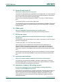
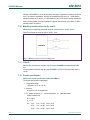
 IMPORTANT NOTICE Dear customer, As from February 2nd 2009, ST and Ericsson have merged Ericsson Mobile Platforms and ST‐NXP Wireless into a 50/50 joint venture "ST‐Ericsson". As a result, the following changes are applicable to the attached document. ● Company name ‐ ST‐NXP Wireless is replaced with ST‐Ericsson. ● Copyright ‐ the copyright notice at the bottom of each page “© ST‐NXP Wireless 200x ‐ All rights reserved”, shall now read: “© ST‐Ericsson, 2009 ‐ All rights reserved”. ● Web site ‐ http://www.stnwireless.com is replaced with www.stericsson.com ● Contact information ‐ the list of sales offices previously obtained at http://www.stnwireless.com , is now found at www.stericsson.com under Contacts If you have any questions related to the document, please contact our nearest sales office or [email protected]. Thank you for your cooperation and understanding. AN10051
PDIUSBD12 frequently asked questions
Rev. 05 — 19 February 2009
Application note
Document information
Info
Content
Keywords
pdiusbd12; usb, universal serial bus; faq
Abstract
This document contains frequently asked questions related to the PDIUSBD12.
ST-NXP Wireless
AN10051
ST-NXP Wireless
PDIUSBD12 FAQs
Revision history
Rev
Date
Description
05
20090219
Globally changed NXP Semiconductors and NXP to ST-NXP Wireless. Also updated the legal text.
04
20070307
Fourth release. Updated Section 1.2 and Table 1.
03
20060707
Third release. Updated Table 1.
02
20051205
Second release.
Section 2.3: Changed the following statement under the second question from ““the device may
enter test mode”” to “the device will enter test mode. Also see Section 5.13.”
Added Section 5.13.
01
20051110
First release.
Contact information
For additional information, please visit: http://www.stnwireless.com
For sales office addresses, please send an email to: [email protected]
AN10051_5
Application note
© ST-NXP Wireless. All rights reserved.
Rev. 05 — 19 February 2009
2 of 17
AN10051
ST-NXP Wireless
PDIUSBD12 FAQs
1. General product information
1.1 Current consumption
How much current does the PDIUSBD12 consume?
During normal operation, the PDIUSBD12 consumes 15 mA. In suspend mode, the
PDIUSBD12 internally shuts off blocks that are non-essential, allowing an operating
current of 15 µA. This is particularly important for bus-powered systems because
Universal Serial Bus Specification requires the suspend current as 500 µA or less. Also
see Section 3.1.
The PDIUSBD12 offers bus-powered capability because it can go into deep sleep,
drawing only 15 µA.
1.2 USB compliance
Is the PDIUSBD12 compliant to USB 2.0?
The PDIUSBD12 is only used as a physical layer and a basic protocol layer interface. It
complies with Universal Serial Bus Specification Rev. 2.0 (full-speed).
2. Power up
2.1 Suspend output
What is the suspend output on power-up?
The SUSPEND pin is LOW right after the PDIUSBD12 is powered up.
2.2 Default clock output
What is the default clock output on power-up?
The default clock output frequency is 4 MHz.
2.3 Power-on reset
How is the power-on reset provided to the PDIUSBD12?
The PDIUSBD12 has a built-in Power-On Reset (POR) circuit. Typically, the RESET_N
pin can directly be connected to VCC. In applications such as Personal Digital Assistant
(PDA) and Digital Still Camera (DSC), in which devices are battery operated, the
PDIUSBD12 is ‘always on’ even when it is not in use. ElectroStatic Discharge (ESD),
possibly caused by handling or storage, can cause the PDIUSBD12 to enter an
indeterminate state. To avoid this, it is recommended that you use an external controlled
source, such as a microcontroller or microprocessor, to provide reset to the PDIUSBD12,
instead of directly connecting the PDIUSBD12 to VCC. An added advantage is that reset
is easily done. For example, in a PDA, the PDIUSBD12 can be reset whenever data
transfer is required through the USB using HotSync application.
What must be the width of the reset pulse in the PDIUSBD12?
The external reset pulse width must be at least 500 µs. When the RESET_N pin is LOW,
ensure that the CS_N pin is in inactive state; otherwise, the device will enter test mode.
Also see Section 5.13.
AN10051_5
Application note
© ST-NXP Wireless. All rights reserved.
Rev. 05 — 19 February 2009
3 of 17
AN10051
ST-NXP Wireless
PDIUSBD12 FAQs
Can the PDIUSBD12 be immediately accessed after the power-on reset?
After reset, wait for at least 3 ms, before accessing the PDIUSBD12 registers. This will
allow sufficient time for the crystal clock to stabilize.
3. Suspend
3.1 Suspend current ratings
What are the suspend current ratings for the PDIUSBD12?
Universal Serial Bus Specification requires bus-powered devices to draw less than
500 µA during suspend mode. To meet this stringent requirement, the PDIUSBD12 shuts
off non-essential internal blocks in suspend mode. This significantly reduces current
ratings to a maximum of only 15 µA, allowing greater margin for the rest of the hardware
to meet the 500 µA requirement in a typical bus-powered system. In addition, the
PDIUSBD12 supports remote wake-up. A peripheral using the PDIUSBD12 can initiate a
system wake-up as well.
Remark: The 15 µA does not include the mandatory pull-up resistor on the D+ line that
adds 200 µA on all USB devices. Therefore, in total, using the PDIUSBD12 as a USB
front-end will consume a maximum of 215 µA on suspend. The actual measured value is
202 µA. Also see Section 1.1.
3.2 Entering suspend
When does the system go into suspend?
When the host requests the system to go into suspend, or when the host itself is in
suspend, USB lines are in idle mode. The electrical translation of this idle mode on the
D+ and D− lines is a HIGH and a LOW, respectively. This assumes that the device has
been connected to the USB bus, with a pull-up resistor on the D+ line.
In addition, when the device is unconnected, it goes into idle mode, if the D+ line is pulled
to HIGH and the D− line is pulled to LOW.
With no activity on the USB bus, the PDIUSBD12 will start to count the absence of three
consecutive Start-Of-Frames (SOFs) and pull the SUSPEND pin to HIGH. The
corresponding SUSPEND_CHANGE bit in the Interrupt register is also set.
3.3 Exiting suspend
How does the system get out of suspend?
A USB device can get out of suspend in two ways: host initiated or device initiated.
Host initiated:
When the host recovers from a suspend state, the USB traffic becomes active again
through the SOF every millisecond. The interrupt line from the PDIUSBD12 becomes
active LOW to indicate that there has been a change of condition on suspend. This may
be used to generate a wake-up to your microcontroller.
Device initiated:
To wake up the system using the PDIUSBD12, you can use the Send Resume
command. This will toggle the D+ and D− lines to send a resume signal to the host.
AN10051_5
Application note
© ST-NXP Wireless. All rights reserved.
Rev. 05 — 19 February 2009
4 of 17
AN10051
ST-NXP Wireless
PDIUSBD12 FAQs
3.4 VOUT3.3 on suspend
What is VOUT3.3 on suspend?
On suspend, this value drops to 2.0 V. It is, however, still capable of supplying 10 mA
current.
3.5 CLKOUT frequency
What is the CLKOUT frequency during suspend?
The behavior of the output clock is configured based on the Configuration Byte written
using the Set Mode command (F3h). See Table 1.
Table 1.
Output clock behavior depending on the Configuration Byte setting
Configuration byte
CLKOUT
No LazyClock
Clock running
0 (on)
0 (off)
CLKOUT switches to LazyClock on suspend. The output
frequency is 18 kHz to 48 kHz. The Phase-Locked Loop
(PLL) clock switches off to reduce current consumption.
1 (off)
0 (off)
CLKOUT stops on suspend. The PLL clock is off.
0 (on)
1 (on)
CLKOUT switches to LazyClock on suspend. The output
frequency is 18 kHz to 48 kHz. The PLL clock remains on.
1 (off)
1 (on)
The suspend state does not affect the CLKOUT frequency
with this configuration.
3.6 1 MΩ resistors in USB-EPP demo
Why are the 1 MΩ resistors required in the USB-EPP demo kit?
In a self-powered system, when the USB cable is disconnected from the host, the D+ and
D− lines will effectively be floating. In a noisy environment, for example, inside a scanner
in which there are many high-current components, some switching will occur on the D+
and D− lines because of the induced noise. This will sometimes mislead the Serial
Interface Engine (SIE) into believing that a resume signal was generated from the host,
causing the PDIUSBD12 to exit the suspend state because to a false resume.
A 1 MΩ pull-down resistor is added to the D− line. Another 1 MΩ pull-up resistor is
connected to the D+ line. Note that there is an error in USB-EPP kit schematics. The pullup and pull-down resistors must follow what is mentioned here.
3.7 Behavior of the SUSPEND pin
Explain the behavior of the SUSPEND pin that is shown as an input as well as an
output.
The SUSPEND pin is a bidirectional pin.
• As an input: When the PDIUSBD12 device is in suspend, the internal registers of
device PDIUSBD12 cannot be accessed. If there is a need to access the device, the
microcontroller can pull the SUSPEND pin to LOW to wake up the device and then
access it. This is how the SUSPEND pin is used as an input.
• As an output: The PDIUSBD12 device can enter suspend as follows: When the host
requests the device to go into suspend, or when the host itself is in suspend, USB
AN10051_5
Application note
© ST-NXP Wireless. All rights reserved.
Rev. 05 — 19 February 2009
5 of 17
AN10051
ST-NXP Wireless
PDIUSBD12 FAQs
lines are in idle mode. The electrical translation of this idle mode on the D+ and D−
lines is a HIGH and a LOW, respectively. This assumes that the device is connected
to the USB bus with a pull-up resistor on the D+ line. In addition, when the device is
unconnected, the device also goes to idle mode, if the D+ line is pulled to HIGH and
the D− line is pulled to LOW. With no activity on the USB bus, the PDIUSBD12 will
start to count the absence of three consecutive SOFs and pull the SUSPEND pin
HIGH. This is how the SUSPEND pin is used as an output.
4. Clocking
4.1 Clockout frequency
What is the available clockout frequency?
The clockout (CLKOUT) frequency can be set through the clock division factor, using the
Set Mode command (F3h). See Table 2.
The output frequency is based on the equation:
CLKOUT = 48 / (N + 1) MHz, where N is clock division factor
Table 2.
CLKOUT frequency depending on the clock division factor
N clock division factor
CLKOUT
00h
48 MHz (maximum clocking frequency of the PDIUSBD12)
01h
24 MHz
02h
16 MHz
03h
12 MHz
04h
9.6 MHz
….
…
0Ah
4.36 MHz
0Bh
4 MHz (power-up value, default CLKOUT frequency, minimum
clocking frequency)
4.2 Suspend CLKOUT frequency
What is the suspend CLKOUT frequency?
See Section 3.
4.3 Start-up time of CLKOUT
What is the start-up time of CLKOUT?
The CLKOUT frequency is derived from the oscillator: pins XTAL1 and XTAL2. The startup time for CLKOUT depends on the start-up time of the crystal oscillator. This has been
measured to be typically below 2 ms. The reset circuit must be designed to be active for
2 ms to be properly reset because some microcontrollers, for example, the 8051 family,
use synchronous reset.
AN10051_5
Application note
© ST-NXP Wireless. All rights reserved.
Rev. 05 — 19 February 2009
6 of 17
AN10051
ST-NXP Wireless
PDIUSBD12 FAQs
4.4 Passive components on the crystal circuit
What are the passive components used on the crystal circuit for the PDIUSBD12?
To allow quicker starting of the clock, reduce C2 (22 pF). The jitter, however, increases
as C2 is reduced. Two capacitors 22 pF and 68 pF must be used.
4.5 Clocking V(p-p)
What is clocking V(p-p) to be fed to the XTAL1 pin?
The clocking voltage can only take a peak-to-peak voltage of 3.3 V because the internal
oscillator is built on a 3.3 V core. Therefore, to use a 5 V external oscillator, it must be
tied to the XTAL1 pin through a 1 kΩ resistor.
5. Interfacing
5.1 Transfer speed on the parallel interface
What is the fastest transfer speed achievable on the parallel interface?
For data back-to-back access, that is, for both read and write, maintain a minimum cycle
time of 500 ns. See Fig 1.
Fig 1. Data back-to-back access
If it is from a write command to a read-or-write data, then the access time must be at
least 600 ns. This also applies to a read-or-write data to a write command. See Fig 2,
Fig 3, Fig 4 and Fig 5. For example, Clear Buffer or Validate Buffer.
Fig 2. Write command to write data
AN10051_5
Application note
© ST-NXP Wireless. All rights reserved.
Rev. 05 — 19 February 2009
7 of 17
AN10051
ST-NXP Wireless
PDIUSBD12 FAQs
Fig 3. Write command to read data
Fig 4. Write data to write command
Fig 5. Read data to write command
5.2 Transferring data from host to device
How does DMA work when data is to be transferred from the host to the device?
When the PDIUSBD12 is set to DMA mode, on receiving a full packet of data from
endpoint 2, DMREQ is asserted to allow the DMA controller to retrieve data from the
AN10051_5
Application note
© ST-NXP Wireless. All rights reserved.
Rev. 05 — 19 February 2009
8 of 17
AN10051
ST-NXP Wireless
PDIUSBD12 FAQs
internal buffer of the PDIUSBD12. The DMA controller must assert the READ_N of the
PDIUSBD12. The PDIUSBD12 does not have any internal buffer to keep track of how
many bytes have been transferred using DMA.
5.3 Transferring data from device to host
How does DMA work when data is to be transferred from the device to the host?
When the PDIUSBD12 is set to DMA mode, there are two conditions in which data from
the buffer will be transferred to the host on an IN token:
• When the internal buffer of endpoint 2 is full (64 bytes), or
• When the EOT_N signal is asserted on the last packet that is transferred through
DMA.
DMREQ is asserted once the internal buffer is empty and when the DMA Enable register
is set. Data is swept to the internal buffer when DMACK_N and DMREQ are both active
at WR_N.
An external DMA controller generates the EOT_N signal when the data count goes to
zero. If the EOT_N signal is not present, it is recommended that you have an external
counter to generate EOT_N in the last packet.
5.4 Single DMA transfer and burst DMA
What is the difference between single DMA transfer mode and burst DMA mode?
The behavior of DMREQ and DMACK_N are different for single and burst modes. For
graphic depiction of single and burst modes, refer to Section 15 of the PDIUSBD12
Universal Serial Bus interface device with parallel bus data sheet.
In single DMA transfer mode, DMREQ is asserted for every RD_N or WR_N strobe.
Therefore, the number of bytes transferred can be counted based on the falling edge of
DMREQ.
In burst DMA mode, DMREQ is asserted through the burst length that is defined based
on the DMA burst information given in the Set DMA command (FBh).
Table 3.
DMA configuration register setting
DMA configuration register
Remarks
Bit 1
Bit 0
0
0
Single DMA transfer mode
0
1
Burst DMA mode. Four bytes of data transferred on every
assertion of DMREQ, unless prematurely ended by EOT_N.
1
0
Burst DMA mode. Eight bytes of data transferred on every
assertion of DMREQ, unless prematurely ended by EOT_N.
1
1
Burst DMA mode. 16 bytes of data transferred on every
assertion of DMREQ, unless prematurely ended by EOT_N.
AN10051_5
Application note
© ST-NXP Wireless. All rights reserved.
Rev. 05 — 19 February 2009
9 of 17
AN10051
ST-NXP Wireless
PDIUSBD12 FAQs
5.5 PDIUSBD12 voltage input
Does the PDIUSBD12 take 5 V or 3.3 V input?
The PDIUSBD12 can take either 5 V or 3.3 V input. To operate the IC at 5 V, supply a
5 V voltage to the VCC pin only and leave the VOUT3.3 pin open, decoupled with
capacitor. To operate the IC at 3.3 V, supply a 3.3 V voltage to both the VCC and
VOUT3.3 pins.
5.6 Output voltage swing
What is the output voltage swing?
There are typically two output types on the PDIUSBD12: open drain and normal driving.
The driving strength for each is specified in the data sheet. The voltage swing of an
open-drain output depends on the pull-up resistor on which it is tied.
Table 4 shows the voltage swing when pin VCC of the PDIUSBD12 is powered from 5 V.
Table 4.
Voltage swing based on 5 V
Pin name
Type
Description
Voltage swing
DATA[7:0]
IO2
Input or output with driving strength of 2 mA
5V
SUSPEND
OD4
Open-drain, can sink 4 mA
Depends on pull-up
CLKOUT
O2
Output with 2 mA drive
5V
INT_N
OD4
Open-drain, can sink 4 mA
Depends on pull-up
GL_N
OD8
Open-drain, can sink 8 mA
Not applicable
DMREQ
O4
Output with 4 mA drive
5V
Table 5 shows the voltage swing when the VCC pin of the PDIUSBD12 is powered from
3.3 V.
Table 5.
Voltage swing based on 3.3 V
Pin name
Type
Description
Voltage swing
DATA[7:0]
IO2
Input or output with driving strength of 2 mA
3.3 V
SUSPEND
OD4
Open-drain, can sink 4 mA
Depends on pull-up
CLKOUT
O2
Output with 2 mA drive
3.3 V
INT_N
OD4
Open-drain, can sink 4 mA
Depends on pull-up
GL_N
OD8
Open-drain, can sink 8 mA
Not applicable
DMREQ
O4
Output with 4 mA drive
3.3 V
Remark: When VCC of the PDIUSBD12 is powered from 3.3 V, the internal regulator
shuts off. All voltage regulation must be done externally. Therefore, a 3.3 V source must
be applied to both the VCC and VOUT3.3 pins.
AN10051_5
Application note
© ST-NXP Wireless. All rights reserved.
Rev. 05 — 19 February 2009
10 of 17
AN10051
ST-NXP Wireless
PDIUSBD12 FAQs
5.7 Using VOUT3.3 to drive other parts of the circuit
Can I use VOUT3.3 to drive other parts of my circuit?
The VOUT3.3 pin is provided to supply the pull-up voltage of 1.5 kΩ resistor. You can
also opt to use the internal SoftConnect 1 resistor. Loading the VOUT3.3 pin apart from
this resistor is not recommended.
5.8 CS_N and DACK_N
Can CS_N and DACK_N be active at the same time?
Do not write or read by asserting CS_N during DMA when DACK_N is active.
5.9 Level trigger or edge trigger
Should level trigger or edge trigger be used on the PDIUSBD12?
The PDIUSBD12 INTERRUPT pin remains LOW as long as the Interrupt register is nonzero. Therefore, the microcontroller must be configured to be level trigger on interrupt.
5.10 VBUS sensing functionality
How must EOT_N be connected to accomplish a VBUS sensing functionality?
In a self-powered system, when the USB connection is removed, there may not be any
indication to the microcontroller that the USB cable is disconnected. To detect a
disconnection, the EOT_N pin has dual functionality, that is, to function as an EOT (EndOf-Transfer) during DMA mode and to detect VBUS sensing. VBUS is the 5 V power supply
pin from the USB connector. For the VBUS sensing, EOT_N is connected to VBUS through
a 1 kΩ resistor and a 1 MΩ bleeding resistor to leak charges. This is to ensure that
EOT_N goes to zero when VBUS is removed.
So, when the device is in self-powered mode and when the host is off, even if the USB
cable is connected, the device will check the non-availability of VBUS through the EOT_N
pin, and switch off the internal SoftConnect resistor. This ensures that the PDIUSBD12 is
disconnected and does not unnecessarily power the D+ line.
5.11 ALE
How to use the ALE pin of the PDIUSBD12?
When the ALE pin of the PDIUSBD12 is connected to the ALE pin of the microcontroller,
and the address bus and the data bus are multiplexed, this pin is used by the internal
logic to strobe in information to differentiate between command and data on the parallel
bus. An even address means writing data to or reading data from the PDIUSBD12, and
an odd address means writing command to the PDIUSBD12. CS_N must be pulled to
LOW during data communications.
A0 will not be used and must be connected to HIGH in this instance.
5.12 CS_N
Can the CS_N pin of the PDIUSBD12 be connected to ground all the time?
The PDIUSBD12 must be treated like any other microprocessor-based device. CS_N is
connected so that the PDIUSBD12 can share the system bus with other devices. In some
instance, CS_N may be grounded all the time. For example, when the PDIUSBD12 is the
only device residing on the system bus. If the system bus is shared, additional circuitry
1
SoftConnect is a trademark of ST-NXP Wireless.
AN10051_5
Application note
© ST-NXP Wireless. All rights reserved.
Rev. 05 — 19 February 2009
11 of 17
AN10051
ST-NXP Wireless
PDIUSBD12 FAQs
may be required to separate the PDIUSBD12 from other resources through
RD_N/WR_N, if CS_N must be grounded.
Example: To glue MC68331 with the PDIUSBD12, the tRHCH and tWHCH timing for the chip
select output must be delayed to match the timing of the PDIUSBD12. In this instance,
CS_N of the PDIUSBD12 can be grounded, and RD_N/WR_N may be all you need. To
separate other devices that share the same bus, glue logic can be implemented on
RD_N/WR_N that is going to the PDIUSBD12.
5.13 Entering test mode
How can the PDIUSBD12 enter test mode?
The PDIUSBD12 will enter test mode when either of these conditions is met:
• When the RESET_N pin is LOW and the CS_N pin is toggled, or
• When the CS_N pin is LOW and the RESET_N pin is toggled.
Therefore, to prevent the PDIUSBD12 from entering test mode, make sure that when the
RESET_N pin is LOW, the CS_N pin is in inactive state. Similarly, when the CS_N pin is
LOW, the RESET_N pin is in inactive state.
6. Programming the PDIUSBD12
6.1 SoftConnect
What is SoftConnect?
The Set Mode register at F3h has a bit that directly connects to the pull-up resistor on the
D+ USB line. When the bit is logic 1, it means that the pulled-up resistor is enabled.
Therefore, a host or a hub will detect that something is plugged on its USB port, even
though it has physically been connected before the command was issued.
SoftConnect allows the microcontroller to finish its initialization routine before notifying
the host of its presence. This is especially valuable in a bus-powered device in which the
5 V power supply must first be stable before enumeration.
To force the host to perform re-enumeration, the microcontroller can initiate a soft
disconnect by setting the Set Mode SoftConnect bit to logic 0. In doing so, the host is
forced to reload the host device driver, allowing a device initiated upgrade without user
intervention to disconnect and connect the USB cable.
6.2 Set address or enable
What is the difference between set address or enable and SoftConnect?
The set address or enable is required to enable the SIE to respond to the USB request
that is directed towards the address preset through the set address or enable. Without
enabling, the PDIUSBD12 will not respond with an ACK or NAK token, even though the
request is directed to its preset address.
6.3 Configuring the DMA register
How to configure the DMA register?
On power-up, the DMA register may be used to check for read or write error. It is the only
register that is available to read and write. Note that on power-up, the auto-reload bit
cannot be set, and the DMA enable bit when set does not pull up the DMREQ pin.
AN10051_5
Application note
© ST-NXP Wireless. All rights reserved.
Rev. 05 — 19 February 2009
12 of 17
AN10051
ST-NXP Wireless
PDIUSBD12 FAQs
The DMA register will be cleared on a bus reset. Therefore, initialized settings to the
DMA register will be lost. It is recommended that you set the DMA register to the
intended value only after the device has been configured.
7. Others
7.1 Double buffering
What is double buffering?
Double buffering on endpoint 2 allows data to be source or sink on the USB bus while the
internal buffer is being read or written by the microcontroller or the DMA controller. This
increases the overall throughput because the host does not need to wait for the internal
buffer to be cleared or filled before feeding or extracting the next packet.
When data is to be extracted from the USB device to the host, the switching from one
buffer that was filled up by the microcontroller to the sending buffer at the USB end is
done transparent to the microcontroller. The microcontroller does not need to keep track
of which buffer to use because it always uses the same register to access the IN buffer.
When data is to be received from the host to the USB device, the switching from one
buffer that was read by the microcontroller to the receiving buffer at the USB end is done
transparent to the microcontroller. The microcontroller does not need to keep track of
which buffer to use because it always uses the same register to access the OUT buffer.
7.2 Internal buffer size
What is the internal buffer size of the PDIUSBD12?
The total number of bytes of the internal buffer dedicated for USB transfer is 320 bytes.
Table 6.
Internal buffer size
Total bytes
320
Endpoint 0
= 16 (IN) + 16 (OUT)
Endpoint 1
+
16 (IN) + 16 (OUT)
Endpoint 2
+
[16 (IN) + 16 (OUT)] x 2 (double buffered)
7.3 EMI issues
Are there any EMI issues that need to be taken into consideration?
ElectroMagnetic Interference (EMI) issues are very broad subject to be covered in this
document. In general, add ferrite beads on VBUS and the ground at the input side of the
USB connector. One such part is BLM32A07.
It is recommended that you have capacitive coupling from the USB shield to the electrical
ground.
7.4 Resistor value for the GoodLink 2 LED
What resistor value is recommended for the GoodLink LED?
This depends on brightness of the LED that you want, and also on the brightness and
current rating of the LED. Any value from 100 Ω to 1 kΩ is normally acceptable. The
evaluation kit recommends a value of 470 Ω.
2
GoodLink is a trademark of ST-NXP Wireless.
AN10051_5
Application note
© ST-NXP Wireless. All rights reserved.
Rev. 05 — 19 February 2009
13 of 17
AN10051
ST-NXP Wireless
PDIUSBD12 FAQs
7.5 Vendor ID and Product ID
What are the Vendor ID and the Product ID?
The Vendor ID (VID) identifies the manufacturer of the USB product. It is used to load the
INF file that contains the text string of the manufacturer and information on which device
driver to load on Microsoft Windows operating system.
The VID can be obtained by registering with USB-IF. The VID for ST-NXP Wireless is
0471.
The Product ID (PID) is unique to each USB product.
The VID and PID can be set by changing the device descriptors in firmware. This is good
for product differentiation as customers maintain their own product identity on Windows
operating system.
7.6 6 MHz crystal
Why is the PDIUSBD12 implemented based on a 6 MHz crystal?
The 6 MHz crystal lowers the risk of having EMI problems during production.
7.7 D12Test.exe report
Why does ST-NXP Wireless test application D12Test.exe report a varying data
transfer rate?
The calculation of the real-time transfer rate is made on every block of 16 kB. The actual
derivation formula used is:
Transfer speed (B/s) = 16 x 1024 / time spent (seconds).
Where time spent is the completion time of transfer minus the initiated time. The
Microsoft Windows 98 operating system provides a 1 ms resolution on time spent. In
addition, a random overhead is incurred because of system calls from user mode to
kernel mode. In total, a 2 ms ambiguity will put the variance of the transfer rate as about
20 %.
Whatever the reported transfer rate, often the host is the bottleneck. A LeCroy analyzer
can be used to verify that the PDIUSBD12 is fully utilizing the allocation provide by the
host.
7.8 Isochronous and bulk pipe
What is the allocation difference between an isochronous and bulk pipe?
An isochronous pipe guarantees bandwidth, regardless of data integrity. A bulk pipe
guarantees data integrity, but delivery is based on ‘first require, first allocate’. Therefore,
on a heavy USB traffic, the bulk pipe may be starved.
7.9 Implications of adding 1 MΩ leaking resistors
Are there any implications on the signaling quality on adding 1 MΩ leaking
resistors on the PDIUSBD12 demo board?
All the signals on the physical layer of USB are designed to be single-end terminated. At
any one time, there can only be a transmitter and a receiver. The transmitter, or the
driver, is required to have an output impedance of between 28 Ω and 44 Ω. At the
receiving end, the receiver must present an input impedance of greater than 300 kΩ,
excluding termination.
AN10051_5
Application note
© ST-NXP Wireless. All rights reserved.
Rev. 05 — 19 February 2009
14 of 17
AN10051
ST-NXP Wireless
PDIUSBD12 FAQs
When the PDIUSBD12 is in the driving state, the output impedance is between 29 Ω and
44 Ω. The effective impedance, inclusive of the parallel pull-up at D+ of 1.5 kΩ and the
parallel pull-down at D+ and D− of 1 MΩ, does not vary much with the driving impedance.
During receiving state, the total impedance is greater than 300 kΩ, even with the 1 MΩ
leakage resistor is present.
7.10 Matching resistor values for D+ and D–
What values of matching resistors must be used for the D+ and D– lines?
Place 18 Ω resistor in series on the D+ and D− lines.
Fig 6. Matching resistor on the D+ and D− lines
7.11 Chip ID
What is the command to read the chip ID of the PDIUSBD12 and what is the chip
ID?
The command to read the chip ID of the PDIUSBD12 is FDh and the expected value is
1012h.
7.12 Crystal specification
What is the crystal specification of the PDIUSBD12?
The crystal specification fundamental:
• Temperature range:
±50 ppm (−20 ºC to +70 ºC)
• Accuracy:
±50 ppm at +25 ºC temperature
• R1: series resistance, Cp:
shunt capacitance, CL: load capacitance
6 MHz fundamental
R1 < 100 Ω,
Cp < 7 pF
CL= 8 pF
Cx1 = 15 pF, Cx2 = 15 pF
12 pF
Cx1 = 22 pF, Cx2 = 22 pF
18 pF
Cx1 = 33 pF, Cx2 = 33 pF
AN10051_5
Application note
© ST-NXP Wireless. All rights reserved.
Rev. 05 — 19 February 2009
15 of 17
AN10051
ST-NXP Wireless
PDIUSBD12 FAQs
8. Legal information
Please Read Carefully:
Information in this document is provided solely in connection with ST-NXP products. ST-NXP Wireless NV and its subsidiaries (“ST-NXP”)
reserve the right to make changes, corrections, modifications or improvements, to this document, and the products and services described
herein at any time, without notice.
All ST-NXP products are sold pursuant to ST-NXP’s terms and conditions of sale.
Purchasers are solely responsible for the choice, selection and use of the ST-NXP products and services described herein, and ST-NXP
assumes no liability whatsoever relating to the choice, selection or use of the ST-NXP products and services described herein. No license,
express or implied, by estoppel or otherwise, to any intellectual property rights is granted under this document. If any part of this document
refers to any third party products or services it shall not be deemed a license grant by ST-NXP for the use of such third party products or
services, or any intellectual property contained therein or considered as a warranty covering the use in any manner whatsoever of such third
party products or services or any intellectual property contained therein.
UNLESS OTHERWISE SET FORTH IN ST-NXP’S TERMS AND CONDITIONS OF SALE ST-NXP DISCLAIMS ANY EXPRESS OR
IMPLIED WARRANTY WITH RESPECT TO THE USE AND/OR SALE OF ST-NXP PRODUCTS INCLUDING WITHOUT LIMITATION
IMPLIED WARRANTIES OF MERCHANTABILITY, FITNESS FOR A PARTICULAR PURPOSE (AND THEIR EQUIVALENTS UNDER THE
LAWS OF ANY JURISDICTION), OR INFRINGEMENT OF ANY PATENT, COPYRIGHT OR OTHER INTELLECTUAL PROPERTY RIGHT.
UNLESS EXPRESSLY APPROVED IN WRITING BY AN AUTHORIZED ST-NXP REPRESENTATIVE, ST-NXP PRODUCTS ARE NOT
RECOMMENDED, AUTHORIZED OR WARRANTED FOR USE IN MILITARY, AIR CRAFT, SPACE, LIFE SAVING, OR LIFE SUSTAINING
APPLICATIONS, NOR IN PRODUCTS OR SYSTEMS WHERE FAILURE OR MALFUNCTION MAY RESULT IN PERSONAL INJURY,
DEATH, OR SEVERE PROPERTY OR ENVIRONMENTAL DAMAGE. ST-NXP PRODUCTS WHICH ARE NOT SPECIFIED AS
"AUTOMOTIVE GRADE" MAY ONLY BE USED IN AUTOMOTIVE APPLICATIONS AT USER’S OWN RISK.
Resale of ST-NXP products with provisions different from the statements and/or technical features set forth in this document shall immediately
void any warranty granted by ST-NXP for the ST-NXP product or service described herein and shall not create or extend in any manner
whatsoever, any liability of ST-NXP.
ST-NXP and the ST-NXP logo are trademarks or registered trademarks of ST-NXP in various countries.
Information in this document supersedes and replaces all information previously supplied.
The ST-NXP logo is a registered trademark of ST-NXP Wireless. All other names are the property of their respective owners.
© 2009 ST-NXP Wireless - All rights reserved
ST-NXP Wireless group of companies
Belgium - Brazil - Canada - China - Czech Republic - Finland - France - Germany - India - Italy - Japan - Korea - Malaysia - Mexico Netherlands - Singapore - Sweden - Switzerland - Taiwan - United Kingdom - United States of America
www.stnwireless.com
AN10051_5
Application note
© ST-NXP Wireless. All rights reserved.
Rev. 05 — 19 February 2009
16 of 17
AN10051
ST-NXP Wireless
PDIUSBD12 FAQs
9. Contents
1. 1.1 1.2 2. 2.1 2.2 2.3 3. 3.1 3.2 3.3 3.4 3.5 3.6 3.7 4. 4.1 4.2 4.3 4.4 4.5 5. 5.1 5.2 5.3 5.4 5.5 5.6 5.7 5.8 5.9 5.10 5.11 5.12 5.13 6. 6.1 6.2 6.3 7. 7.1 7.2 7.3 7.4 General product information .............................. 3 Current consumption .......................................... 3 USB compliance ................................................. 3 Power up .............................................................. 3 Suspend output .................................................. 3 Default clock output ............................................ 3 Power-on reset ................................................... 3 Suspend ............................................................... 4 Suspend current ratings ..................................... 4 Entering suspend ............................................... 4 Exiting suspend .................................................. 4 VOUT3.3 on suspend ............................................. 5 CLKOUT frequency ............................................ 5 1 MΩ resistors in USB-EPP demo...................... 5 Behavior of the SUSPEND pin ........................... 5 Clocking ............................................................... 6 Clockout frequency ............................................ 6 Suspend CLKOUT frequency ............................. 6 Start-up time of CLKOUT ................................... 6 Passive components on the crystal circuit.......... 7 Clocking V(p-p) ..................................................... 7 Interfacing ............................................................ 7 Transfer speed on the parallel interface ............. 7 Transferring data from host to device ................. 8 Transferring data from device to host ................. 9 Single DMA transfer and burst DMA .................. 9 PDIUSBD12 voltage input ................................ 10 Output voltage swing ........................................ 10 Using VOUT3.3 to drive other parts of the circuit
......................................................................... 11 CS_N and DACK_N ......................................... 11 Level trigger or edge trigger ............................. 11 VBUS sensing functionality................................. 11 ALE .................................................................. 11 CS_N................................................................ 11 Entering test mode ........................................... 12 Programming the PDIUSBD12.......................... 12 SoftConnect ..................................................... 12 Set address or enable ...................................... 12 Configuring the DMA register ........................... 12 Others ................................................................. 13 Double buffering ............................................... 13 Internal buffer size ............................................ 13 EMI issues........................................................ 13 Resistor value for the GoodLink LED ............... 13 7.5 7.6 7.7 7.8 7.9 7.10 7.11 7.12 8. 9. Vendor ID and Product ID ................................14 6 MHz crystal ....................................................14 D12Test.exe report ...........................................14 Isochronous and bulk pipe................................14 Implications of adding 1 MΩ leaking resistors ..14 Matching resistor values for D+ and D– ...........15 Chip ID .............................................................15 Crystal specification .........................................15 Legal information ..............................................16 Contents .............................................................17 Please be aware that important notices concerning this document and the product(s)
described herein, have been included in the section 'Legal information'.
© ST-NXP Wireless 2009. All rights reserved.
For more information, please visit: http://www.stnwireless.com
For sales office addresses, email to: [email protected]
Date of release: 19 February 2009
Document identifier: AN10051_5