1
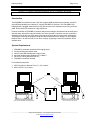
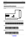
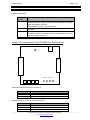
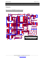
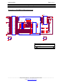
Philips Semiconductors
Interconnectivity
1 September 1998
PDIUSBD12 Evaluation Board (PC Kit)
User’s Manual
Rev. 2.1
_______________________________________________________________________________________________
Philips Semiconductors - Asia Product Innovation Centre
Visit http://www.flexiusb.com
Interconnectivity
Page 2 of 14
PDIUSBD12 Evaluation Board (PC Kit) User’s Manual
Rev. 2.1
This is a legal agreement between you (either an individual or an entity) and Philips Semiconductors.
By accepting this product, you indicate your agreement to the disclaimer specified as follows:
DISCLAIMER
PRODUCT IS DEEMED ACCEPTED BY RECIPIENT. THE PRODUCT IS PROVIDED
“AS IS” WITHOUT WARRANTY OF ANY KIND. TO THE MAXIMUM EXTENT
PERMITTED BY APPLICABLE LAW, PHILIPS SEMICONDUCTORS FURTHER
DISCLAIMS ALL WARRANTIES, INCLUDING WITHOUT LIMITATION ANY
IMPLIED WARRANTIES OF MERCHANT ABILITY, FITNESS FOR A PARTICULAR
PURPOSE, AND NONINFRINGEMENT. THE ENTIRE RISK ARISING OUT OF THE
USE OR PERFORMANCE OF THE PRODUCT AND DOCUMENTATION REMAINS
WITH THE RECIPIENT. TO THE MAXIMUM EXTENT PERMITTED BY
APPLICABLE LAW, IN NO EVENT SHALL PHILIPS SEMICONDUCTORS OR ITS
SUPPLIERS BE LIABLE FOR ANY CONSEQUENTIAL, INCIDENTAL, DIRECT,
INDIRECT, SPECIAL, PUNITIVE, OR OTHER DAMAGES WHATSOEVER
(INCLUDING, WITHOUT LIMITATION, DAMAGES FOR LOSS OF BUSINESS
PROFITS, BUSINESS INTERRUPTION, LOSS OF BUSINESS INFORMATION, OR
OTHER PECUNIARY LOSS) ARISING OUT OF THIS AGREEMENT OR THE USE OF
OR INABILITY TO USE THE PRODUCT, EVEN IF PHILIPS SEMICONDUCTORS HAS
BEEN ADVISED OF THE POSSIBILITY OF SUCH DAMAGES.
_______________________________________________________________________________________________
Philips Semiconductors - Asia Product Innovation Centre
Visit http://www.flexiusb.com
Interconnectivity
Page 3 of 14
PDIUSBD12 Evaluation Board (PC Kit) User’s Manual
REV. 2.1
TABLE OF CONTENTS
DISCLAIMER .............................................................................................................2
TABLE OF CONTENTS .............................................................................................3
INSTALLATION OF PDIUSBD12 EVALUATION BOARD ........................................4
Introduction.................................................................................................................................................... 4
System Requirements..................................................................................................................................... 4
Installation...................................................................................................................................................... 5
Jumper’s setting on PDIUSBD12 ISA bridging board ................................................................................... 5
Location of key components on the PDIUSBD12 evaluation board. .............................................................. 6
Installation of firmware, INF and driver........................................................................................................ 7
Using the Host Applet .................................................................................................................................... 7
HARDWARE DESCRIPTION.....................................................................................9
Block Diagram................................................................................................................................................ 9
I/O Mapping................................................................................................................................................... 9
Connectors.................................................................................................................................................... 10
PAL Equations ............................................................................................................................................. 11
Address and command decoder................................................................................................................... 11
Schematics.................................................................................................................................................... 12
Schematics for PDIUSBD12 evaluation board ............................................................................................ 12
Schematic for PDIUSBD12 ISA bridging board.......................................................................................... 13
Bill of Materials............................................................................................................................................ 14
Bill of materials of the PDIUSBD12 evaluation board................................................................................. 14
Bill of materials of the PDIUSBD12 ISA bridging board............................................................................. 14
_______________________________________________________________________________________________
Philips Semiconductors - Asia Product Innovation Centre
Visit http://www.flexiusb.com
Interconnectivity
Page 4 of 14
PDIUSBD12 Evaluation Board (PC Kit) User’s Manual
REV. 2.1
INSTALLATION OF PDIUSBD12 EVALUATION BOARD
Introduction
The PDIUSBD12 evaluation kit uses 2 PC as a complete USB development environment, a host PC
with USB host capability and a device PC running PDIUSBD12’s firmware. The PDIUSBD12 ISA
bridging board is plugged inside the device PC and connects to the evaluation board using a 25-wire
cable. So the device PC behaves as a big USB device.
Features evaluation of PDIUSBD12, firmware and product prototype development can be easily done
with this setup, without the resource limitation of a micro-controller. Customers can also connect the
evaluation board to their own CPU and bus through the 25-wire cable for final product development.
The firmware is carefully developed for high rate data transmission and is written in C, that supports
Borland Turbo C for x86 and Keil C51 for 8031 currently. Supporting to other CPU platforms will be
available soon.
System Requirements
1.
2.
3.
4.
5.
6.
PDIUSBD12 evaluation board and ISA bridging board;
25-wire shielding data switch cable;
Host PC with USB motherboard or add-on card;
Microsoft Windows 98 or Windows NT 5.0 Beta 2;
Device PC running Microsoft DOS 6.x;
PDIUSBD12 evaluation diskette.
For firmware development:
1. X86 CPU platform: Borland Turbo C++ 3.0 or above;
2. 8031: Keil C51 4.0 or above.
PDIUSBD12 Evaluation Disk
D1
D1 2TES
2
D1 TES T.EX
2T T.S E
ES
T.I YS
NF
E
.EX
2FW
D1
USB Cable
25-Wire Cable
D12
Mouse
Device PC with PDIUSBD12 ISA Bridging Board
Mouse
PDIUSBD12 Evaluation Board
Host PC with USB host Controller
_______________________________________________________________________________________________
Philips Semiconductors - Asia Product Innovation Centre
Visit http://www.flexiusb.com
Interconnectivity
Page 5 of 14
PDIUSBD12 Evaluation Board (PC Kit) User’s Manual
REV. 2.1
Installation
Jumper’s setting on PDIUSBD12 ISA bridging board
The PDIUSBD12 ISA bridging board is plugged inside the device PC. It will occupy I/O, IRQ and DMA
resources of the device PC. To avoid possible conflicts in settings, we suggest removal of all the
unnecessary cards from the device PC. Sound card and network card may cause conflict in IRQ and
DMA setting.
J2
ON
JP5 JP6
S1
1
8
JP1 JP2
JP3 JP4
Switch S1 sets the base I/O address for the D12 evaluation board. Default base address is 0x368.
The D12 evaluation board occupies 8 I/O locations. A0 to A2 are decoded on the D12 evaluation
board. Switch S1 sets the address decoding of A3 to A9. Please notice that a switch ‘ON’ is logic ‘0’.
SW(n)
Address
Default
1
X
OFF
2
A3
OFF
3
A4
ON
4
A5
OFF
5
A6
OFF
6
A7
ON
7
A8
OFF
8
A9
OFF
Jumpers JP1 and JP2 set the IRQ number for the D12 evaluation board. Default setting is IRQ5 or
JP1 is shorted.
IRQ Number
Jumper’s Setting
Default
IRQ5
JP1
ON
IRQ7
JP2
OFF
Jumpers JP3 to JP6 set the DMA number for the D12 evaluation board. Default setting is DMA3 or
JP4 and JP6 are shorted. Please note that a respective pair of jumpers is needed to set a particular
DMA channel.
DMA Number
Jumper’s Setting
Default
DMA1
JP3, JP5
OFF, OFF
DMA3
JP4, JP6
ON, ON
_______________________________________________________________________________________________
Philips Semiconductors - Asia Product Innovation Centre
Visit http://www.flexiusb.com
Interconnectivity
Page 6 of 14
PDIUSBD12 Evaluation Board (PC Kit) User’s Manual
REV. 2.1
Possible conflict table:
IRQ or DMA
Number
IRQ5
IRQ7
DMA1
DMA3
Possible Conflict
Creative SoundBlaster™ and compatible sound cards always occupy
this IRQ by default. If this kind of sound card is installed, you should
check its settings or remove it.
Some network cards may also use this IRQ.
Used by parallel port by default. May cause printing problem on
device PC.
Creative SoundBlaster™ and compatible sound cards always occupy
this DMA by default. If this kind of sound card is installed, you should
check its settings or remove it.
No conflict.
Location of key components on the PDIUSBD12 evaluation board.
J1
D1
J2
J3
D5 D4 D3 D2
S4
S3
S2
S1
See the table below for the list of connectors.
Connector
J1
J2
J3
Descriptions
USB upstream connector
DB25 data bus connector
Extension board connector
See the table below for the list of switch and LEDs.
Name
Descriptions
S1, S2, S3, S4
Test switches
GoodLink™ LED
D1
D2, D3, D4, D5
Test LEDs
_______________________________________________________________________________________________
Philips Semiconductors - Asia Product Innovation Centre
Visit http://www.flexiusb.com
Interconnectivity
Page 7 of 14
PDIUSBD12 Evaluation Board (PC Kit) User’s Manual
REV. 2.1
Installation of firmware, INF and driver
The firmware, D12FW.EXE, runs on the device PC under DOS mode. When D12FW starts, it lights up
test LEDs on the evaluation board for 1 second. This means that the I/O address setting is correct.
And the evaluation board is disconnected and re-connected to USB by SoftConnectTM. If this is the
first time that the evaluation board is connected to host PC, host OS Device Manager will prompt
installation of INF and driver. Select the location of D12TEST.INF and D12TEST.SYS and complete
installation procedure.
Some useful key command is supported when the firmware is running.
Key
ESC
ENTER
i
v
Operation
Disconnect USB and quit PDIUSBD12 firmware.
Reconnect USB using SoftConnectTM.
Display firmware status information.
Switch on/off verbose mode, normally turned off for faster operation.
Using the Host Applet
The test applet, D12TEST.EXE, exercises all PDIUSBD12 endpoints. Testing of control endpoints can
be further done by standard USB Chapter 9 test programs.
The operation of each endpoint is designed according to its nature that is supported in PDIUSBD12.
Generic in and generic out endpoints has max packet size of 16 bytes and supports I/O access only.
So they are suitable for small size and low rate data transfer like keyboard and logic controls. The
main endpoints have max packet size of 64 bytes or 128 bytes with double buffering and DMA
support. So they are suitable for high data rate, large size data transfer.
_______________________________________________________________________________________________
Philips Semiconductors - Asia Product Innovation Centre
Visit http://www.flexiusb.com
Interconnectivity
Page 8 of 14
PDIUSBD12 Evaluation Board (PC Kit) User’s Manual
REV. 2.1
See the table below for the description of endpoints operations on PDIUSBD12 evaluation board.
Endpoint
Number
1
Endpoint
Type
Generic
In
1
Generic
Out
2
Main In
Main Out
Operations
This pipe is defined as Interrupt In pipe. The PDIUSBD12 evaluation
board sends key press/release data packet to the host when test keys
are pressed or released. The firmware uses I/O accesses on this
endpoint.
This pipe is defined as Interrupt Out pipe. Data packet received from
host is interpreted as LED control and the D12 evaluation board
firmware will light up the corresponding LED. The firmware uses I/O
accesses on this endpoint.
These pipes are defined as Bulk In/Out endpoints. Test applet and the
PDIUSBD12 evaluation board supports 3 test modes: loop-back mode,
print mode and scan mode. The firmware uses DMA for data transfer
on these endpoints.
Main endpoints support 3 different test modes:
1. Scan mode: The PDIUSBD12 evaluation board acts like a scanner. It sends data packets to the
host PC as fast as possible. This mode is used to evaluate the maximal Bulk In transfer rate.
2. Print mode: The PDIUSBD12 evaluation board acts like a printer. It receives data packets from
the host PC as fast as possible. This mode is used to evaluate the maximal Bulk Out transfer rate.
3. Loop back mode: In this mode, the PDIUSBD12 evaluation board receives data packets on Main
Out endpoint and sends them back to the host PC on Main In endpoint. This mode is used to test
the data integrity of transfers.
The “Buffer Size” setting on the test applet is determined by the firmware and hardware ability of the
evaluation board. For PC kit, the maximal size is limited to 64000; On USB-EPP kit, this is limited to
16384.
The “Repeat Times” for loop-back test controls the numbers of iterations of loop-back, which is useful
for debugging. “-1” means it is infinite.
_______________________________________________________________________________________________
Philips Semiconductors - Asia Product Innovation Centre
Visit http://www.flexiusb.com
Interconnectivity
Page 9 of 14
PDIUSBD12 Evaluation Board (PC Kit) User’s Manual
REV. 2.1
HARDWARE DESCRIPTION
System Block
Diagram of D12
Evaluation Kit
On USB host side, a
sample application program
D12TEST.EXE and a
general purpose minidriver
D12TEST.SYS are
provided.
USB Host PC
25 Pin Interface
1. VCC, GND
2. D0 - D7
3. ADDRESS ENABLE
4. IOW, IOR, IRQ, RESET
5. DREQ, DACK, EOT
D12 Sample Applet
D12TEST.EXE
Customer's System
On device side, sample firmware
D12FW.EXE is provided for
running on device PC. The
firmware is written in C for easily
portable to other CPU platforms.
25
Pin
I/F
CPU,
Memory,
and DMA
Controller
D12 Evaluation Board
USB Device PC
D12 Sample Driver
D12TEST.SYS
Test
Key
General
Input port
Test
LED
General
Output port
Command
and Address
Decoder
25
Pin
I/F
D12 ISA Bridging Board
USBD
USB Host Controller
Driver
25
Pin
I/F
Bi-direction
Bus
Transceiver
PDIUSBD12
USB Host Controller
ISA
Slot
DIP
Switches
and
Jumpers
Block Diagram
Above block diagram shows 5 main components on the PDIUSBD12 evaluation board. Beside bus
transceiver, address/command decoder and PDIUSBD12, a general input port and a general output
port are included in the design. These input and output ports are designed for test purposes, such as
test switches and test LEDs. They also act as glue logic to adapt the PDIUSBD12 to the ISA bus. For
example, ISA interrupt is edge triggered, but PDIUSBD12 interrupt is level triggered. The MSB of the
general output port is used as interrupt enable to convert level triggered interrupt to edge triggered.
I/O Mapping
PDIUSBD12 evaluation board uses 8 I/O addresses:
Offset
0
1
2
3
4 to 7
Usage
D12 data register, R/W
D12 command register, W only
General input port, R only
General output port, W only
Reserved for expansion board
_______________________________________________________________________________________________
Philips Semiconductors - Asia Product Innovation Centre
Visit http://www.flexiusb.com
Interconnectivity
Page 10 of 14
PDIUSBD12 Evaluation Board (PC Kit) User’s Manual
REV. 2.1
Bit description for general input port:
Bit
0
1
2
3
4
5
6
7
Usage
Key S1, ‘0’ for pressed
Key S2, ‘0’ for pressed
Key S3, ‘0’ for pressed
Key S4, ‘0’ for pressed
D12 GoodLinkTM pin state
USB bus power state, ‘1’ for USB VBUS present
D12 SUSPEND pin state
D12 INT_N pin state
Bit description for general output port:
Bit
0
1
2
3
4
5
6
7
Usage
LED D2, ‘1’ lights up LED
LED D3, ‘1’ lights up LED
LED D4, ‘1’ lights up LED
LED D5, ‘1’ lights up LED
Reserved
Reserved
Suspend control, ‘1’ forces D12 SUSPEND pin low
Interrupt enable, ‘1’ enables interrupt
Connectors
25 wire connector for PDIUSBD12 evaluation board:
Pin
1
2
3
4
5
6
7
8
9
10
Type
POWER
POWER
I/O
I/O
I/O
I/O
I/O
O
I/O
I
11
12
I/O
I
13
14
I/O
I
15
16
I/O
I
Description
VCC
GND
DATA7
Zero Wait State
DATA6
Reserved
DATA5
CLKOUT: This line is connected to PDIUSBD12 CLKOUT pin.
DATA4
-AD_EN: This line is the decoder output for address decoding A3 to
A9. This signal is active low when PDIUSBD12 evaluation board I/O
address is selected.
DATA3
RESET: This line is used to reset or initialize system logic upon
power-up and is active high.
DATA2
-IOW: This command line instructs an I/O device to read the data on
the data bus. It may be driven by the processor or the DMA controller.
This signal is active low.
DATA1
-IOR: This command line instructs an I/O device to drive its data onto
the data bus. It may be driven by the processor or the DMA controller.
This signal is active low.
_______________________________________________________________________________________________
Philips Semiconductors - Asia Product Innovation Centre
Visit http://www.flexiusb.com
Interconnectivity
Page 11 of 14
PDIUSBD12 Evaluation Board (PC Kit) User’s Manual
REV. 2.1
17
18
I/O
I
19
20
I
I
21
22
I
O
23
24
I
O
25
POWER
DATA0
T/C, Terminal Count: This line provides a pulse when terminal count
for any DMA channel is reached. This signal is active high.
ADDR2
-DACK: This line is used to acknowledge DMA request and is active
low.
ADDR1
DRQ: This line is asynchronous channel request used by peripheral
devices to gain DMA service. A DMA request is generated by bringing
DRQ line to an active high.
ADDR0
IRQ: This line is raising edge triggered. An interrupt request is
generated by raising this line high and hold until it is acknowledged by
the processor.
GND
PAL Equations
Address and command decoder
/** Inputs **/
Pin 1 = ADDR2;
Pin 2 = ADDR1;
Pin 3 = ADDR0;
Pin 4 = !IOW;
Pin 5 = !IOR;
Pin 6 = !DACK;
Pin 7 = !AD_EN;
Pin 8 = RESET;
Pin 9 = INT_N;
Pin 11 = INT_EN;
/** Outputs **/
Pin 12 = IRQ;
Pin 13 = RESET_N;
Pin 14 = RD_N;
Pin 15 = WAIT;
Pin 16 = !CS_D12;
Pin 17 = !WR_273;
Pin 18 = !RD_244;
Pin 19 = !DIR_245;
/** Logic Equations **/
!DIR_245 = (!AD_EN & !DACK) # !IOR # RESET;
!RD_244 = !AD_EN # !(!ADDR2 & ADDR1 & !ADDR0) # !IOR;
!WR_273 = !AD_EN # !(!ADDR2 & ADDR1 & ADDR0) # !IOW;
!CS_D12 = !AD_EN # !(!ADDR2 & !ADDR1) # (!IOW & !IOR);
RESET_N = !RESET;
IRQ = !INT_N & INT_EN;
WAIT.OE = CS_D12;
WAIT = RESET;
RD_N = !IOR;
_______________________________________________________________________________________________
Philips Semiconductors - Asia Product Innovation Centre
Visit http://www.flexiusb.com
Interconnectivity
Page 12 of 14
PDIUSBD12 Evaluation Board (PC Kit) User’s Manual
REV. 2.1
Schematics
Schematics for PDIUSBD12 evaluation board
+
VCC
C1
4.7 TANT
C13
S5
V_BUS
VCC R1
470
BUS POWERED
J2
DB25
1
3
5
7
9
11
13
15
17
19
21
23
25
Shell to
DATA[0..7]
DATA7
DATA6
DATA5
DATA4
DATA3
DATA2
DATA1
DATA0
ADDR2
ADDR1
ADDR0
R4 R5
4.7K 4.7K
2
4
6
8
10
12
14
16
18
20
22
24
VCC
CLKOUT
-AD_EN
RESET
-IOW
-IOR
T/C
-DACK
DRQ
IRQ
GND
470P, Ceramic
PDIUSBD12
U1
1
D0
A0
2 DATA0
D1
VOUT3.3
3 DATA1
D2
D+
4 DATA2
D3
DATA3
D5
VCC
6 GND
D4
XTAL2
7 DATA4
D5
XTAL1
8 DATA5
D6
GL_N
9 DATA6
D7
RESET_N
10 DATA7
EOT_N
11 ALE
-CS_D12
CS_N
DMACK_N
SUSPEND 12
DMREQ
13 SUSPEND
CLKOUT
WR_N
INT_N 14
INT_N
RD_N
C3
0.1
D1
GREEN
28
27
26
25
24
23
22
21
20
19
18
17
16
15
ADDR0
L1
Ferrite Bead
V_BUS
+ C2
4.7 TANT
J1
1
2
3
4
5
R2
22 1%
Y1 6MHz
XTAL2
XTAL1
C16
0.1
22 1%
C5
47P
-DACK
DRQ
-IOW
-IOR
R7 R8 R9 R10
10K 10K 10K 10K
C6
22P
OSC1
4
G O
UP_CONN
L2
Ferrite Bead
R3
VBUS
DD+
GND
SHIELD
C14
0.1
VCC
5
VCC
1
19
1
A1
A2
A3
A4
A5
A6
A7
A8
B1
B2
B3
B4
B5
B6
B7
B8
G
DIR
18
17
16
15
14
13
12
11
D0
D1
D2
D3
D4
D5
D6
D7
D0
D1
D2
D3
D4
D5
D6
D8
D7
U2
74LS245
-DIR_245
1
2
3
4
5
6
7
8
9
11
ADDR2
ADDR1
ADDR0
-IOW
-IOR
-DACK
-AD_EN
RESET
C15
1000P
I1
I2
I3
I4
I5
I6
I7
I8
I9
I10
O1
O2
O3
O4
O5
O6
O7
O8
18
16
14
12
9
7
5
3
1Y1
1Y2
1Y3
1Y4
2Y1
2Y2
2Y3
2Y4
1A1
1A2
1A3
1A4
2A1
2A2
2A3
2A4
1G
2G
D[0..7]
2
3
4
5
6
7
8
9
DATA0
DATA1
DATA2
DATA3
DATA4
DATA5
DATA6
DATA7
D0
D1
D2
D3
D4
D5
D6
D7
U5
16L8
INT_EN
INT_N
3
4
7
8
13
14
17
18
11
1
D1
D2
D3
D4
D5
D6
D7
D8
S3
* OSC1 is optional replacement
for Y1, C5 and C6.
R11
1K
1
Q1
Q2
Q3
Q4
Q5
Q6
Q7
Q8
S4
V_BUS
1
19
2
5
6
9
12
15
16
19
2
R12
470
U4A
74LS05
VCC
R13
470
D2
RED
R16
1M
D3
RED
R14
470
D4
RED
U4C
74LS05
5
13
6
12
9
8
U4D
74LS05
11
1
3
5
7
9
11
13
15
17
19
J3
CON20A
2
4
6
8
10
12
14
16
18
20
CLKOUT
INT_N
RESET_N
-AD_EN
-IOW
-IOR
ADDR2
ADDR1
ADDR0
10
U6
74HCT273
C8
0.1
C9
0.1
C10
0.1
C11
0.1
C12
0.1
D5
RED
4
VCC
D7
D6
D5
D4
D3
D2
D1
D0
R15
470
U4B
74LS05
3
U4F
74LS05
CLK
CLR
S1
8
S2
2
4
6
8
11
13
15
17
U3
74HCT244
19
18 -RD_EVAL
17 -WR_EVAL
16 -CS_D12
15 ZERO_WAIT
14
13 RESET_N
12 IRQ
N V
U4E
74LS05
VCC
Title
D12 EVALUATION BOARD
+ C7
10 TANT
Size
A
Date:
Document Number
D12-EVAL-200
Thursday, April 23, 1998
Rev
2.00
Sheet
1
of
1
_______________________________________________________________________________________________
Philips Semiconductors - Asia Product Innovation Centre
Visit http://www.flexiusb.com
Interconnectivity
Page 13 of 14
PDIUSBD12 Evaluation Board (PC Kit) User’s Manual
REV. 2.1
Schematic for PDIUSBD12 ISA bridging board
VCC J2
DB25
J1
CON AT62
A1
A2
A3
A4
A5
A6
A7
A8
A9
A10
A11
A12
A13
A14
A15
A16
A17
A18
A19
A20
A21
A22
A23
A24
A25
A26
A27
A28
A29
A30
A31
DATA[0..7]
DATA7
DATA6
DATA5
DATA4
DATA3
DATA2
DATA1
DATA0
ADDR2
ADDR1
ADDR0
RP1
20K
S1
SW DIP-8
8
7
6
5
4
3
2
1
VCC
8
7
6
5
4
3
2
1
B1
B2
B3
B4
B5
B6
B7
B8
B9
B10
B11
B12
B13
B14
B15
B16
B17
B18
B19
B20
B21
B22
B23
B24
B25
B26
B27
B28
B29
B30
B31
I/O CH CK
DATA7
DATA6
DATA5
DATA4
DATA3
DATA2
DATA1
DATA0
I/O CH RDY
AEN
ADDR19
ADDR18
ADDR17
ADDR16
ADDR15
ADDR14
ADDR13
ADDR12
ADDR11
ADDR10
ADDR9
ADDR8
ADDR7
ADDR6
ADDR5
ADDR4
ADDR3
ADDR2
ADDR1
ADDR0
7
6
5
4
3
2
1
C
GND
VCC RESET
+5V
IRQ2
-5V
DRQ2
-12V
ZERO_WA IT
+12V
GND
-MEMW
-MEMR
-IOW
-IOR
-DACK3
DRQ3
-DACK1
DRQ1
-DACK0
CLOCK
IRQ7
IRQ6
IRQ5
IRQ4
IRQ3
-DACK2
T/C
VCC
ALE
+5V
OSC
GND
U1
1
9
10
11
12
13
14
15
16
18
16
14
12
9
7
5
3
17
15
13
11
8
6
4
2
G
VCC
Q7
Q6
Q5
Q4
Q3
Q2
Q1
Q0
P7
P6
P5
P4
P3
P2
P1
P0
C1
0.1
2
4
6
8
10
12
14
16
18
20
22
24
ZERO_WA IT
-AD_EN
VCC
RESET
-IOW
-IOR
R1
T/C
-DACK
10K
DRQ
IRQ
GND
IRQ5
IRQ7
JP1
JP2
DRQ1
DRQ3
-DACK1
-DACK3
P=Q
19
JP3
JP4
JP5
JP6
-AD_EN
74HCT688
ADDR[0..2]
VCC
+ C2
4.7u
1
3
5
7
9
11
13
15
17
19
21
23
25
Shell to
VCC
+ C3
4.7u
C4
0.1
C5
0.1
Title
D12 ISA BRIDGING BOARD
Size
A
Date:
Document Number
D12-ISA-200
Tuesday, February 24, 1998
Rev
2.00
Sheet
1
of
1
_______________________________________________________________________________________________
Philips Semiconductors - Asia Product Innovation Centre
Visit http://www.flexiusb.com
Interconnectivity
Page 14 of 14
PDIUSBD12 Evaluation Board (PC Kit) User’s Manual
REV. 2.1
Bill of Materials
Bill of materials of the PDIUSBD12 evaluation board
Item
1
2
3
4
5
6
7
8
9
10
11
12
13
14
15
16
17
18
19
20
21
22
23
24
25
26
27
28
29
Quantity
2
8
1
1
1
1
1
1
4
1
1
1
2
1
5
2
2
4
1
1
4
1
1
1
1
1
1
1
1
Reference
C2,C1
C3,C8,C9,C10,C11,C12,C14,C16
C5
C6
C7
C13
C15
D1
D2,D3,D4,D5
J1
J2
J3
L1,L2
OSC1
R1,R12,R13,R14,R15
R2,R3
R4,R5
R7,R8,R9,R10
R11
R16
S1,S2,S3,S4
S5
U1
U2
U3
U4
U5
U6
Y1
Part
4.7 TANT
0.1
47P
22P
10 TANT
470P, Ceramic
1000P
GREEN
RED
UP_CONN
DB25
CON20A
Ferrite Bead
Crystal Oscillator
470
22 1%
4.7K
10K
1K
1M
SW PUSHBUTTON
BUS POWERED
PDIUSBD12
74LS245
74HCT244
74LS05
16L8
74HCT273
6MHz
Bill of materials of the PDIUSBD12 ISA bridging board
Item
1
2
3
4
5
6
7
8
9
Quantity
3
2
6
1
1
1
1
1
1
Reference
C1,C4,C5
C2,C3
JP1,JP2,JP3,JP4,JP5,JP6
J1
J2
RP1
R1
S1
U1
Part
0.1
4.7u
JUMPER
CON AT62
DB25
20K
10K
SW DIP-8
74HCT688
_______________________________________________________________________________________________
Philips Semiconductors - Asia Product Innovation Centre
Visit http://www.flexiusb.com