1
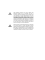
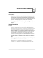
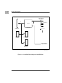
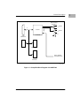
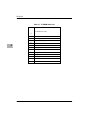
MVIP302
Eight-Channel EIA-232 IndustryPack¨
and
MVIP303
Eight-Channel EIA-422 IndustryPack¨
User’s Manual
(MVIP302/D1)
Notice
While reasonable efforts have been made to assure the accuracy of this document,
Motorola, Inc. assumes no liability resulting from any omissions in this document, or
from the use of the information obtained therein. Motorola reserves the right to revise
this document and to make changes from time to time in the content hereof without
obligation of Motorola to notify any person of such revision or changes.
No part of this material may be reproduced or copied in any tangible medium, or
stored in a retrieval system, or transmitted in any form, or by any means, radio,
electronic, mechanical, photocopying, recording or facsimile, or otherwise, without the
prior written permission of Motorola, Inc.
It is possible that this publication may contain reference to, or information about
Motorola products (machines and programs), programming, or services that are not
announced in your country. Such references or information must not be construed to
mean that Motorola intends to announce such Motorola products, programming, or
services in your country.
Restricted Rights Legend
If the documentation contained herein is supplied, directly or indirectly, to the U.S.
Government, the following notice shall apply unless otherwise agreed to in writing by
Motorola, Inc.
Use, duplication, or disclosure by the Government is subject to restrictions as set forth
in subparagraph (c)(1)(ii) of the Rights in Technical Data and Computer Software
clause at DFARS 252.227-7013.
Motorola, Inc.
Computer Group
2900 South Diablo Way
Tempe, Arizona 85282
Preface
Much of the information in the MVIP302 Eight Channel EIA-232 IndustryPack and
MVIP303 Eight Channel EIA-422 IndustryPack UserÕs Manual is adapted from the IPOctal Serial User Manual and the IP-Octal 422 User Manual, published by GreenSpring
Computers, Inc. Permission to reproduce this material has been granted by
GreenSpring Computers, Inc.
The following Motorola publication is referenced in this manual. If not shipped with
this product, it may be purchased by contacting your local Motorola sales ofÞce.
Document Title
Motorola Publication Number
MVME162 Embedded Controller UserÕs Manual
MVME162/D
This manual also references the IndustryPack Interface SpeciÞcation. The SpeciÞcation
may be purchased from: VITA-USA, 10229 N. Scottsdale Rd., Ste. B, Scottsdale, Az.
85253-1437; (602) 951-8866.
Motorola¨ and the Motorola symbol are registered trademarks of Motorola, Inc.
IndustryPack¨ is a registered trademark of GreenSpring Computers, Inc.
All other products mentioned in this document are trademarks or registered
trademarks of their respective holders.
© Copyright Motorola 1993
All Rights Reserved
Printed in the United States of America
June 1993
Safety Summary
Safety Depends On You
The following general safety precautions must be observed during all phases of
operation, service, and repair of this equipment. Failure to comply with these
precautions or with speciÞc warnings elsewhere in this manual violates safety
standards of design, manufacture, and intended use of the equipment. Motorola, Inc.
assumes no liability for the customer's failure to comply with these requirements.
The safety precautions listed below represent warnings of certain dangers of which
Motorola is aware. You, as the user of the product, should follow these warnings and
all other safety precautions necessary for the safe operation of the equipment in your
operating environment.
Do Not Operate in an Explosive Atmosphere.
Do not operate the equipment in the presence of ßammable gases or fumes. Operation
of any electrical equipment in such an environment constitutes a deÞnite safety hazard.
Keep Away From Live Circuits.
Operating personnel must not remove equipment covers. Only Factory Authorized
Service Personnel or other qualiÞed maintenance personnel may remove equipment
covers for internal subassembly or component replacement or any internal adjustment.
Do not replace components with power cable connected. Under certain conditions,
dangerous voltages may exist even with the power cable removed. To avoid injuries,
always disconnect power and discharge circuits before touching them.
Do Not Service or Adjust Alone.
Do not attempt internal service or adjustment unless another person, capable of
rendering Þrst aid and resuscitation, is present.
Do Not Substitute Parts or Modify Equipment.
Because of the danger of introducing additional hazards, do not install substitute parts
or perform any unauthorized modiÞcation of the equipment. Contact your local
Motorola representative for service and repair to ensure that safety features are
maintained.
Dangerous Procedure Warnings.
Warnings, such as the example below, precede potentially dangerous procedures
throughout this manual. Instructions contained in the warnings must be followed. You
should also employ all other safety precautions which you deem necessary for the
operation of the equipment in your operating environment.
!
WARNING
Dangerous voltages, capable of causing death, are present in
this equipment. Use extreme caution when handling,
testing, and adjusting.
!
WARNING
!
WARNING
This equipment generates, uses, and can radiate radio
frequency energy and if not installed and used in
accordance with the documentation for this product, may
cause interference to radio communications. It has been
tested and found to comply with the limits for a Class A
Computing Device pursuant to Subpart J of Part 15 of FCC
rules, which are designed to provide reasonable protection
against such interference when operated in a commercial
environment. Operation of this equipment in a residential
area is likely to cause interference in which case the user, at
the userÕs own expense, will be required to take whatever
measures necessary to correct the interference.
Motorola products are not authorized for use as components
in life support devices or systems intended for surgical
implant into the body or intended to support or sustain life.
Buyer agrees to notify Motorola of any such intended end
use whereupon Motorola shall determine availability and
suitability of its product or products for the use intended.
Contents
Chapter 1
PRODUCT DESCRIPTION
Introduction ..........................................................................................................1-1
General Description .............................................................................................1-1
MVIP302..........................................................................................................1-1
MVIP303..........................................................................................................1-4
Chapter 2
ADDRESSING
Introduction ..........................................................................................................2-1
VMEbus Addressing............................................................................................2-1
Chapter 3
I/O PIN ASSIGNMENTS
Introduction ..........................................................................................................3-1
MVIP302 EIA-232 I/O Pin Assignments ..........................................................3-1
MVIP303 EIA-422 I/O Pin Assignments ..........................................................3-4
Chapter 4
LOGIC INTERFACE PIN ASSIGNMENTS
Introduction ..........................................................................................................4-1
Pin Assignments ...................................................................................................4-1
Chapter 5
PROGRAMMING
Introduction ..........................................................................................................5-1
Programming the MVIP302/MVIP303 .............................................................5-1
Chapter 6
ID PROM
Introduction ..........................................................................................................6-1
ID PROM ...............................................................................................................6-1
Chapter 7
USER OPTIONS
Introduction ..........................................................................................................7-1
vii
Strobe Connection Options................................................................................. 7-4
Direct Memory Access (DMA) Options............................................................ 7-4
Appendix A SPECIFICATIONS
Construction and Reliability ............................................................................. A-1
SpeciÞcations ....................................................................................................... A-2
viii
Figures
Figure 1-1.
Figure 1-2.
Figure 1-3.
Figure 4-1.
Figure 4-2.
Figure 7-1.
Figure 7-2.
SimpliÞed Block Diagram of the MVIP302 ..................................1-2
MVIP302 I/O Buffer Circuit...........................................................1-3
SimpliÞed Block Diagram of the MVIP303 ..................................1-5
Logic Interface Pin Assignments for the MVIP302 .....................4-2
Logic Interface Pin Assignments for the MVIP303 .....................4-3
MVIP302 Header Location Diagram.............................................7-2
MVIP303 Header Location Diagram.............................................7-3
ix
x
Tables
Table 2-1. Register Map of SCC2698, Blocks A and B......................................2-2
Table 2-2. Register Map of SCC2698, Blocks C and D.....................................2-3
Table 3-1. MVIP302 EIA-232 I/O PIn Assignments ........................................3-2
Table 3-2. MVIP303 EIA-422 I/O Pin Assignments.........................................3-4
Table 6-1. ID PROM Data (hex) ..........................................................................6-2
Table 7-1. Strobe Connection Options ...............................................................7-4
Table 7-2. DMA Jumper ConÞgurations ...........................................................7-4
xi
xii
PRODUCT DESCRIPTION
1
Introduction
The MVIP302 and MVIP303 are part of the IndustryPack family of modular
I/O components. They are based around the Signetics CMOS SCC2698 Octal
Universal Asynchronous Receiver/Transmitter. This component provides
eight channels of full-duplex asynchronous serial communications, baud rate
generators, state change detect logic, and four 16-bit counter/timers.
A block diagram of the MVIP302 is shown in Figure 1-1; Figure 1-2 illustrates
the MVIP302 I/O Buffer Circuit. A block diagram of the MVIP303 is shown in
Figure 1-3.
General Description
MVIP302
EIA-232-D communication levels are provided by CMOS MC14C88 and
MC14C89 transmitters and receivers. Five signals for each channel on the EIA232-D interface are supported: Transmit Data (TxD), Receive Data (RxD),
Ready-To-Send (RTS), Clear-To-Send (CTS) and ground. The MC14C89
Receivers are biased at 1.5 volts nominally to permit a variety of input signal
levels to be received without additional interface circuitry (see Figure 1-2).
Protection diodes are provided in the ±12 volt supply lines to permit
connection to powered equipment, even if the IndustryPack is unpowered.
Vectored interrupts are fully supported. A common 8-bit vector register is
provided. Channels a,b,c,d interrupt on IRQ0; channels e,f,g,h interrupt on
IRQ1.
DMA is supported on channels c and d. If DMA is used, then the Request-ToSend lines on these two channels are not available .
The IndustryPack is controlled by a single CMOS 22V10 type PAL.
Connection to the MVIP302 is via a standard 50-conductor ribbon cable.
1
Product Description
ONE OF EIGHT
CHANNELS
8
EIA-232-D
OCTART
LOGIC
INTERFACE
ID PROM
SCC2698B
CONTROL PAL
EIGHT GENERAL
PURPOSE INPUTS
VECTOR
REGISTER
10430.00 9306
Figure 1-1. Simplified Block Diagram of the MVIP302
1-2
MVIP302/MVIP303 UserÕs Manual
General Description
+12V
EIA-232-D
SIGNAL OUT
FROM
OCTART
-12V
TO
OCTART
EIA-232-D
SIGNAL IN
22KΩ
-12V
10431.00 93066
Figure 1-2. MVIP302 I/O Buffer Circuit
MVIP302/D1
1-3
1
1
Product Description
MVIP303
EIA-422 communication levels are provided by 26LS31 and 26LS32
transmitters and receivers. Differential transmit data (TxD) and receive data
(RxD) lines are provided, plus ground. EIA-422 communication is preferred
over EIA-232 because it provides significantly higher noise immunity. A
second advantage is that no ±12 volt power is required at either the send or
receive end.
Vectored interrupts are fully supported. A common 8-bit vector register is
provided. Channels a,b,c,d interrupt on IRQ0. Channels e,f,g,h interrupt on
IRQ1.
DMA is supported on channels c and d.
The IndustryPack is controlled by a single CMOS 22V10 type PAL.
Connection to the MVIP303 is via a standard 50-conductor ribbon cable.
1-4
MVIP302/MVIP303 UserÕs Manual
General Description
ONE OF EIGHT
CHANNELS
+
8
OCTART
+
LOGIC
INTERFACE
ID PROM
EIA-422
EIA-422
SCC2698B
CONTROL PAL
EIGHT GENERAL
PURPOSE INPUTS
VECTOR
REGISTER
10432.00 9306
Figure 1-3. Simplified Block Diagram of the MVIP303
MVIP302/D1
1-5
1
ADDRESSING
2
Introduction
The MVIP302 and MVIP303 are accessed using 8-bit bytes at odd locations
only. They are usually accessed in the I/O space. Table 2-1 and Table 2-2 show
the register maps of the MVIP302 and MVIP303. All addresses are offsets from
the I/O base address of the IP, as set on the IP carrier board.
VMEbus Addressing
The SCC2698B Octal UART has four major internal sections, called functional
blocks A through D. Each functional block has two serial channels, one timer,
and one I/O port.
Addressing
2
Table 2-1. Register Map of SCC2698, Blocks A and B
Hex
Dec
Binary
Read
Write
Functional Block A
1
1
0000001
MR1a, MR2a
3
3
0000011
SRa
MR1a, MR2a
CSRa
5
5
0000101
RESERVED
CRa
7
7
0000111
RHRa
THRa
9
9
0001001
IPCRA
ACRA
B
11
0001011
ISRA
IMRA
D
13
0001101
CTUA
CTURA
F
15
0001111
CRLB
CTLRB
11
17
0010001
MR1b, MR2b
MR1b, MR2b
13
19
0010011
SRb
CSRb
15
21
0010101
RESERVED
CRb
17
23
0010111
RHRb
RHRb
19
25
0011001
RESERVED
RESERVED
1B
27
0011011
INPUT PORT A
OPCRA
1D
29
0011101
START C/T A
RESERVED
1F
31
0011111
STOP C/T A
RESERVED
21
33
0100001
MR1c, MR2c
MR1c, MR2c
23
35
0100011
SRc
CSRc
25
37
0100101
RESERVED
CRc
27
39
0100111
RHRc
THRc
29
41
0101001
IPCRB
ACRB
2B
43
0101011
ISRB
IMRB
2D
45
0101101
CTUB
CTURB
2F
47
0101111
CRLB
CTLRB
31
49
0110001
MR1d, MR2d
MR1d, MR2d
33
51
0110011
SRd
CSRd
35
53
0110101
RESERVED
CRd
37
55
0110111
RHRd
THRd
39
57
0111001
RESERVED
RESERVED
3B
59
0111011
INPUT PORT B
OPCRB
3D
61
0111101
START C/T B
RESERVED
3F
63
0111111
STOP C/T B
RESERVED
Functional Block B
2-2
MVIP302/MVIP303 UserÕs Manual
VMEbus Addressing
Table 2-2. Register Map of SCC2698, Blocks C and D
Hex
Dec
Binary
Read
2
Write
Functional Block C
41
65
1000001
MR1e, MR2e
MR1e, MR2e
43
67
1000011
SRe
CSRe
45
69
1000101
RESERVED
CRe
47
71
1000111
RHRe
THRe
49
73
1001001
IPCRC
ACRC
4B
75
1001011
ISRC
IMRC
4D
77
1001101
CTUC
CTURC
4F
79
1001111
CRLC
CTLRC
51
81
1010001
MR1f, MR2f
MR1f, MR2f
53
83
1010011
SRf
CSRf
55
85
1010101
RESERVED
CRf
57
87
1010111
RHRf
THRf
59
89
1011001
RESERVED
RESERVED
5B
91
1011011
INPUT PORT C
OPCRC
5D
93
1011101
START C/T C
RESERVED
5F
95
1011111
STOP C/T C
RESERVED
61
97
1100001
MR1g, MR2g
MR1g, MR2g
63
99
1100011
SRg
CSRg
65
101
1100101
RESERVED
CRg
67
103
1100111
RHRg
THRg
69
105
1101001
IPCRD
ACRD
6B
107
1101011
ISRD
IMRD
6D
109
1101101
CTUD
CTURD
6F
111
1101111
CRLD
CTLRD
71
113
1110001
MR1h, MR2h
MR1h, MR2h
73
115
1110011
SRh
CSRh
75
117
1110101
RESERVED
CRh
77
119
1110111
RHRh
RHRh
79
121
1111001
RESERVED
RESERVED
7B
123
1111011
INPUT PORT D
OPCRD
7D
125
1111101
START C/T D
RESERVED
7F
127
1111111
STOP C/T D
RESERVED
Functional Block D
MVIP302/D1
2-3
I/O PIN ASSIGNMENTS
3
Introduction
This chapter discusses EIA-232 and EIA-422 I/O Pin Assignments. The
MVIP302 EIA-232 I/O wiring pin assignments are shown in Table 3-1; the
MVIP303 EIA-422 I/O pin assignments are shown in Table 3-2.
MVIP302 EIA-232 I/O Pin Assignments
Each channel has five EIA-232-D lines, and each is wired identically at the 50pin connector. The five lines are Ground, Transmit Data output, Receive Data
input, Ready to Send output, and Clear to Send input. The common ground
line for all channels connects to the local logic ground. There are many
programming options. The two modem control lines, RTS and CTS, may also
be used for other modem or terminal control functions or for general purpose
functions.
There is a pullup resistor (1KΩ) to +12 volts available on pin 42. This may be
connected externally to assert a ÒMarkÓ (true) signal into an EIA-232-D line.
Eight general purpose input lines at non-EIA-232 levels are provided on pins
43 through 50. These are unbuffered CMOS logic inputs connected directly to
the SCC2698B. They may be programmed as general purpose inputs or as the
counter/timer external input. The switching threshold for inputs is at TTL
levels (1.5 volts nominal).
C aution
Because these lines are unbuffered, you are cautioned to
observe anti-static rules in handling cabling, the
IndustryPack and all connecting hardware.
External
equipment connected to these lines should be powered up
and down at the same time as the IndustryPack.
I/O Pin Assignments
Table 3-1. MVIP302 EIA-232 I/O PIn Assignments
3
3-2
Pin Number
Channel
Function
Level
1
Channel a
GND
EIA-232-D
2
Channel a
TxD
EIA-232-D
3
Channel a
RxD
EIA-232-D
4
Channel a
RTS
EIA-232-D
5
Channel a
CTS
EIA-232-D
6
Channel b
GND
EIA-232-D
7
Channel b
TxD
EIA-232-D
8
Channel b
RxD
EIA-232-D
9
Channel b
RTS
EIA-232-D
10
Channel b
CTS
EIA-232-D
11
Channel c
GND
EIA-232-D
12
Channel c
TxD
EIA-232-D
13
Channel c
RxD
EIA-232-D
14
Channel c
RTS
EIA-232-D
15
Channel c
CTS
EIA-232-D
16
Channel d
GND
EIA-232-D
17
Channel d
TxD
EIA-232-D
18
Channel d
RxD
EIA-232-D
19
Channel d
RTS
EIA-232-D
20
Channel d
CTS
EIA-232-D
21
Channel e
GND
EIA-232-D
22
Channel e
TxD
EIA-232-D
23
Channel e
RxD
EIA-232-D
24
Channel e
RTS
EIA-232-D
25
Channel e
CTS
EIA-232-D
26
Channel f
GND
EIA-232-D
27
Channel f
TxD
EIA-232-D
MVIP302/MVIP303 UserÕs Manual
MVIP302 EIA-232 I/O Pin Assignments
Table 3-1. MVIP302 EIA-232 I/O PIn Assignments
Pin Number
Channel
Function
Level
28
Channel f
RxD
EIA-232-D
29
Channel f
RTS
EIA-232-D
30
Channel f
CTS
EIA-232-D
31
Channel g
GND
EIA-232-D
32
Channel g
TxD
EIA-232-D
33
Channel g
RxD
EIA-232-D
34
Channel g
RTS
EIA-232-D
35
Channel g
CTS
EIA-232-D
36
Channel h
GND
EIA-232-D
37
Channel h
TxD
EIA-232-D
38
Channel h
RxD
EIA-232-D
39
Channel h
RTS
EIA-232-D
40
Channel h
CTS
EIA-232-D
41
--
GND
--
42
--
+12 pullup
EIA-232-D
43
Channel a
MPI - a
CMOS*
44
Channel b
MPI - b
CMOS*
45
Channel c
MPI - c
CMOS*
46
Channel d
MPI - d
CMOS*
47
Channel e
MPI - e
CMOS*
48
Channel f
MPI - f
CMOS*
49
Channel g
MPI - g
CMOS*
50
Channel h
MPI - h
CMOS*
3
*Note: I/O lines on pins 43-50 are +/-50 µA input current, TTL thresholds.
MVIP302/D1
3-3
I/O Pin Assignments
MVIP303 EIA-422 I/O Pin Assignments
Each channel has five lines, and each is wired identically at the 50-pin
connector. The five lines are: Ground, Transmit Data output Minus, Transmit
Data output Plus, Receive Data input Minus, and Receive Data input Plus. The
common ground line for all channels connects to the local logic ground.
3
Eight general purpose input lines at non-EIA-422 levels are provided on pins
43 through 50. These are unbuffered CMOS logic inputs connected directly to
the SCC2698B. They may be programmed as general purpose inputs or as the
counter/timer external input. The switching threshold for inputs is at TTL
levels (1.5 volts nominal).
C aution
Because these lines are unbuffered, you are cautioned to
observe anti-static rules in handling cabling, the
IndustryPack and all connecting hardware.
External
equipment connected to these lines should be powered up
and down at the same time as the IndustryPack.
Table 3-2. MVIP303 EIA-422 I/O Pin Assignments
3-4
Pin Number
Channel
Function
Level
1
2
Channel a
GND
EIA-422
Channel a
TxDÐ
EIA-422
3
Channel a
TxD+
EIA-422
4
Channel a
RxDÐ
EIA-422
5
Channel a
RxD+
EIA-422
6
Channel b
GND
EIA-422
7
Channel b
TxDÐ
EIA-422
8
Channel b
TxD+
EIA-422
9
Channel b
RxDÐ
EIA-422
10
Channel b
RxD+
EIA-422
11
Channel c
GND
EIA-422
12
Channel c
TxDÐ
EIA-422
13
Channel c
TxD+
EIA-422
14
Channel c
RxDÐ
EIA-422
MVIP302/MVIP303 UserÕs Manual
MVIP303 EIA-422 I/O Pin Assignments
Table 3-2. MVIP303 EIA-422 I/O Pin Assignments
MVIP302/D1
Pin Number
Channel
Function
Level
15
Channel c
RxD+
EIA-422
16
Channel d
GND
EIA-422
17
Channel d
TxDÐ
EIA-422
18
Channel d
TxD+
EIA-422
19
Channel d
RxDÐ
EIA-422
20
Channel d
RxD+
EIA-422
21
Channel e
GND
EIA-422
22
Channel e
TxDÐ
EIA-422
23
Channel e
TxD+
EIA-422
24
Channel e
RxDÐ
EIA-422
25
Channel e
RxD+
EIA-422
26
Channel f
GND
EIA-422
27
Channel f
TxDÐ
EIA-422
28
Channel f
TxD+
EIA-422
29
Channel f
RxDÐ
EIA-422
30
Channel f
RxD+
EIA-422
31
Channel g
GND
EIA-422
32
Channel g
TxDÐ
EIA-422
33
Channel g
TxD+
EIA-422
34
Channel g
RxDÐ
EIA-422
35
Channel g
RxD+
EIA-422
36
Channel h
GND
EIA-422
37
Channel h
TxDÐ
EIA-422
38
Channel h
TxD+
EIA-422
39
Channel h
RxDÐ
EIA-422
40
Channel h
RxD+
EIA-422
41
--
GND
--
3
3-5
I/O Pin Assignments
Table 3-2. MVIP303 EIA-422 I/O Pin Assignments
3
Pin Number
Channel
Function
Level
42
--
no connection
43
Channel a
MPI - a
CMOS*
44
Channel b
MPI - b
CMOS*
45
Channel c
MPI - c
CMOS*
46
Channel d
MPI - d
CMOS*
47
Channel e
MPI - e
CMOS*
48
Channel f
MPI - f
CMOS*
49
Channel g
MPI - g
CMOS*
50
Channel h
MPI - h
CMOS*
*Note: I/O lines on pins 43-50 are +/-50 µA input current, TTL thresholds.
3-6
MVIP302/MVIP303 UserÕs Manual
LOGIC INTERFACE PIN
ASSIGNMENTS
4
Introduction
This chapter provides information on the pin assignments for the MVIP302
(see Figure 4-1) and the MVIP303 (see Figure 4-2).
Pin Assignments
Pins marked n/c are defined by the IndustryPack Interface Specification, but not
used on the MVIP302 or the MVIP303.
Pin Assignments
4
GND
1
26
GND
CLK
2
27
+5V
Reset*
3
28
R/W*
D0
4
29
IDSel*
D1
5
30
DMAReq0
D2
6
31
MEMSel*
D3
7
32
DMAReq1
D4
8
33
INTSel*
D5
9
34
DMAck0*
D6
10
35
IOSel*
D7
11
36
DMAck1*
n/c
12
37
A1
n/c
13
38
n/c
n/c
14
39
A2
n/c
15
40
n/c
n/c
16
41
A3
n/c
17
42
nc
n/c
18
43
A4
n/c
19
44
n/c
n/c
20
45
A5
n/c
21
46
Strobe*
-12V
22
47
A6
+12V
23
48
Ack*
+5V
24
49
n/c
GND
25
50
GND
Note 1 : The no-connect (n/c) signals above are defined by the IndustryPack Logic Interface
Specification, but not used by this IP. See the Specification for more information.
Note 2 : The layout of the pin numbers in this table corresponds to the physical placementof pins
on the IP connector. Thus this table may be used to easily locate the physical pin corresponding
to a desired signal. Pin 1 is marked with a square pad on the IndustryPack.
10433.00 9305
Figure 4-1. Logic Interface Pin Assignments for the MVIP302
4-2
MVIP302/MVIP303 UserÕs Manual
Pin Assignments
GND
1
26
GND
CLK
2
27
+5V
Reset*
3
28
R/W*
D0
4
29
IDSel*
D1
5
30
DMAReq0
D2
6
31
MEMSel*
D3
7
32
DMAReq1
D4
8
33
INTSel*
D5
9
34
DMAck0*
D6
10
35
IOSel*
D7
11
36
DMAck1*
n/c
12
37
A1
n/c
13
38
n/c
n/c
14
39
A2
n/c
15
40
n/c
n/c
16
41
A3
n/c
17
42
n/c
n/c
18
43
A4
n/c
19
44
n/c
n/c
20
45
A5
n/c
21
46
Strobe*
-12V
22
47
A6
+12V
23
48
Ack*
+5V
24
49
n/c
GND
25
50
GND
4
Note 1 : The no-connect (n/c) signals above are defined by the IndustryPack Logic Interface
Specification, but not used by this IP. See the Specification for more information.
Note 2 : The layout of the pin numbers in this table corresponds to the physical placementof pins
on the IP connector. Thus this table may be used to easily locate the physical pin corresponding
to a desired signal. Pin 1 is marked with a square pad on the IndustryPack.
10434.00 9305
Figure 4-2. Logic Interface Pin Assignments for the MVIP303
MVIP302/D1
4-3
PROGRAMMING
5
Introduction
The MVIP302 and MVIP303 are designed around the SCC2698B; all of the
SCC2698B functions are available. Refer to Chapter 2, tables 2-1 and 2-2, for
information on the register maps of the SCC2698B.
Programming the MVIP302/MVIP303
The SCC2698B is divided into four functional blocks lettered A through D.
Each functional block contains two serial channels. The channels are identified
by lower case letters a through h. The SCC2698B contains 64 internal registers,
16 for each functional block. Each of these registers are accessible using a read
or write to the MVIP302 or the MVIP303 I/O space.
The IndustryPack provides an external Interrupt Vector Register. This register
is readable and writable in the memory space of the corresponding IP slot at
any odd byte address using an offset of $01 from the IP memory base address
(as programmed on the carrier board). The 8-bit vector register is normally
programmed by the operating system I/O driver software prior to enabling
interrupts.
The Interrupt Vector Register may also be read on odd bytes in the upper half
of the Industry Pack ID PROM space.
The address offset is IP base + $C1.
However, this register cannot be written in the ID PROM space from the
MVME162 board.
The interrupt service routine polls the SCC2698B to determine the detailed
cause of the interrupt. Function blocks A and B interrupt on IRQ0. Function
blocks C and D interrupt on IRQ1. Refer to the MVME162 Embedded Controller
UserÕs Manual for interrupt mapping to your bus. Note that although two
distinct interrupt levels are provided, there is a single vector for the
IndustryPack.
ID PROM
6
Introduction
This chapter contains information on the ID PROM for the MVIP302 and the
MVIP303. Standard data in the ID PROM is shown in Table 6-1.
ID PROM
Every IndustryPack contains an ID PROM, whose size is at least 32 x 8 bits.
The ID PROM aids in software auto configuration and configuration
management. The user's software, or a supplied driver, may verify that the
device it expects is actually installed at the location it expects, and is nominally
functional. The ID PROM contains the manufacturing revision level of the
IndustryPack. If a driver requires that a particular revision be present, it may
check for it directly.
For more information on ID PROMs, refer to the IndustryPack Logic Interface
Specification.
The location of the ID PROM in the host's address space is dependent upon
which carrier is used. Normally for VMEbus carriers, the ID PROM space is
directly above the IndustryPack's I/O space, or at IP-base + $80. The ID PROM
used is an AMD 27LS19A or equivalent.
ID PROM
Table 6-1. ID PROM Data (hex)
3F
.
.
.
19
17
15
13
11
6
0F
0D
0B
09
07
05
03
01
6-2
(available for user)
CRC
No. of bytes used
Driver ID, high byte
Driver ID, low byte
reserved
Revision
Model No.
Manufacturer ID
ASCII "C"
ASCII "A"
ASCII "P"
ASCII "I"
(26)
(0C)
(00)
(B1)
(10)
(F0)
(43)
(41)
(50)
(49)
MVIP302/MVIP303 UserÕs Manual
USER OPTIONS
7
Introduction
User options consist of connecting to the Strobe pin on the Logic Interface and
making connections to support DMA. Header locations on the MVIP302 are
shown in Figure 7-1; header locations on the MVIP303 are shown in Figure 7-2.
User Options
OSC
SCC2698B
7
E1
E3
E2
10435.00 9306
Figure 7-1. MVIP302 Header Location Diagram
7-2
MVIP302/MVIP303 UserÕs Manual
Introduction
OSC
SCC2698B
7
7
E1
7
E3
E2
10436.00 9306
Figure 7-2. MVIP303 Header Location Diagram
MVIP302/D1
7-3
User Options
Strobe Connection Options
The Strobe pin on the Logic Interface (pin 46) is provided for secondary clock
input or output. This pin may be driven by the Channel a Multi-Purpose
Output from the SCC, or it may be connected to provide for the external input
to the Counter/Timer. These options are shown in Table 7-1. Note that in
most cases some corresponding programming of SCC modes is required. The
SCC may be programmed to drive the connected pin for other functions than
those listed in the Table 7-1. The IndustryPack Logic Interface Specification
restricts the Strobe pin to clock functions, however. Only those functions
listed below should be programmed.
Table 7-1. Strobe Connection Options
7
Header E1
I/O
SCC Pin
Function
1-2
Output
MPOa
Counter/Timer output
1-2
Output
MPOa
Transmit Clock (1X or 16X)
1-2
Output
MPOa
Receive Clock (1X or 16X)
2Ð3
Input
MPI1a
General Purpose Input
2Ð3
Input
MPI1a
Counter/Timer External Input
OUT
none
none
Strobe Pin ßoating (default)
Direct Memory Access (DMA) Options
The MVIP302 and MVIP303 are configured to support minimum Direct
Memory Access (DMA) on channels c and d. To use DMA, program the SCC
for TxRDY or RxRDY on MPOc and/or MPOd (refer to Table 7-2) .
Table 7-2. DMA Jumper Configurations
7-4
Header
SCC Pin
Logic Pin
Function
E2 IN
MPOc
DMAReq0
TxRDY or RxRDY
E3 IN
MPOd
DMAReq1
TxRDY or RxRDY
E2,E3 OUT
--
--
No DMA (default)
MVIP302/MVIP303 UserÕs Manual
SPECIFICATIONS
A
Construction and Reliability
IndustryPacks were conceived and engineered for rugged industrial
environments. The MVIP302 and MVIP303 are constructed out of .062 inch
thick FR4 material. The six copper layers consist of a ground plane, a power
plane and four signal planes.
Surface mounting of components is used extensively. IC sockets for the
control PAL and ID PROM use gold plated screw-machined pins. High
insertion and removal forces are required, which assists in keeping
components in place. If the application requires unusually high reliability or
is in an environment subject to high vibration, the user may solder the four
corner pins of each socketed IC into the socket, using a grounded soldering
iron.
The IndustryPack connectors are keyed, shrouded and gold plated on both
contacts and receptacles. They are rated at 1 Amp per pin, 200 insertion cycles
minimum. These connectors make consistent, correct insertion easy and
reliable.
The IP is optionally secured to the carrier with four metric M2 stainless steel
screws. The heads of the screws are countersunk into the IP. The four screws
provide significant protection against shock, vibration, and incomplete
insertion. For most applications they are not required.
The IndustryPack provides a low temperature coefficient of .89 W/°C for
uniform heat. This is based on the temperature coefficient of the base FR4
material of .31 W/m-°C, and taking into account the thickness and area of the
IP. This coefficient means that if .89 Watts is applied uniformly on the
component side, that the temperature difference between the component and
the solder side is one degree Celsius.
A
Specifications
Specifications
Logic Interface
IndustryPack Logic Interface
Wait States
0 on ID and Interrupts,
1 on SCC accesses
Number of Channels
8
Type of Channels
MVIP302
Full-duplex asynchronous EIA-232-D
MVIP303
Full-duplex asynchronous EIA-422
Baud Rates
18 Þxed rates from 50 to 38.4K
4 user-deÞned rates using timers
Implemented Signals:
A-2
MVIP302
TxD, RxD, RTS, CTS, GND
MVIP303
TxD+, TxD-, RxD+, RxD-, GND
Stop Bits
1, 1.5, 2 in 1/16 bit increments
Clock Source
Local crystal oscillator, or external
Error Detection
Parity, framing, overrun, false start bit, break
Channel Modes
Full duplex, automatic echo, local loopback, remote
loopback
Number of Timers
4
Type of Timers
16-bit, multi-function, programmable
Interrupt Sources
32, maskable, vectored
Interrupt Vector
8 bits, may be independently read/writable
Auxiliary Input Lines
8 TTL/CMOS level inputs, programmable bit input
or state change detect causes interrupt or
counter/external clock input
IP Strobe Options
Timer output, or baud rate clock input, or none
MVIP302/MVIP303 UserÕs Manual
Specifications
Power Requirements:
MVIP302
MVIP303
+5 VDC, 170 mA
+12 VDC, 22 mA
-12 VDC, 9 mA
+5 VDC, 285 mA, typical
+12 VDC, 0 mA
-12 VDC, 0 mA
Dimensions
1.8 by 3.9 by .34 inches maximum
Environmental
Operation temperature: 10 to 55 C
Humidity: 5 to 95% non-condensing
Storage: -10 to +85 C
MVIP302/D1
A-3
A