1
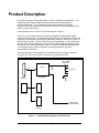
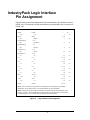
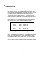
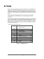
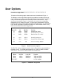
IP-OCTAL-232
Eight Channel RS-232
IndustryPack™
©1999, 2005 SBSTechnologies, Inc.
Subject to change without notice.
Hardware Revision: B
Part # 89002067 Rev. 1.0
20050119
IP-OCTAL-232
Eight Channel RS-232
IndustryPack™
SBS Tecnologies, Inc
1284 Corporate Center Drive
St. Paul, MN 55121
Tel (651) 905-4700
FAX (651) 905-4701
Email:
[email protected]
©1999, 2005 SBS Technologies, Inc.
IndustryPack is a registered trademark of SBS
Technologies, Inc. QuickPack, SDpacK and Unilin are
trademarks SBS Technologies, Inc. PC•MIP is a
trademark of SBS Technologies, Inc. and MEN Mikro
GmbH.
SBS Technologies, Inc acknowledges the trademarks of
other organizations for their respective products
mentioned in this document.
All rights are reserved: No one is permitted to reproduce
or duplicate, in any form, the whole or part of this
document without the express consent of SBS
Technologies. This document is meant solely for the
purpose in which it was delivered.
SBS Technologies reserves the right to make any
changes in the devices or device specifications contained
herein at any time and without notice. Customers are
advised to verify all information contained in this
document.
The electronic equipment described herein generates,
uses, and may radiate radio frequency energy, which can
cause radio interference. SBS Technologies assumes no
liability for any damages caused by such interference.
SBS Technologies’ products are not authorized for use as
critical components in medical applications such as life
support equipment, without the express consent of the
president of SBS Technologies, Inc.
This product has been designed to operate with
IndustryPack, PC•MIP or PMC modules or carriers and
compatible user-provided equipment. Connection of
incompatible hardware is likely to cause serious damage.
SBS Technologies assumes no liability for any damages
caused by such incompatibility.
Table of Contents
Product Description............................................................................................................... 5
VMEbus Addressing ............................................................................................................. 7
NuBus Addressing ................................................................................................................ 9
I/O Pin Assignments.............................................................................................................. 10
IndustryPack Logic Interface................................................................................................. 12
Programming......................................................................................................................... 13
ID PROM............................................................................................................................... 14
User Options ......................................................................................................................... 15
Construction and Reliability .................................................................................................. 16
Repair.................................................................................................................................... 17
Shunt Locations .................................................................................................................... 18
Specifications ........................................................................................................................ 19
List of Figures
Figure 1
Simplified Block Diagram of IP-OCTAL-232 ............................................... 5
Figure 2
I/O Buffer Circuit ......................................................................................... 6
Figure 3
Register Map of SCC2698, Blocks A and B ............................................... 7
Figure 4
Register Map of SCC2698, Blocks C and D............................................... 8
Figure 5
I/O Pin Assignment ..................................................................................... 10
Figure 6
Logic Interface Pin Assignment .................................................................. 12
Figure 7
Location of the Vector Register .................................................................. 13
Figure 8
ID PROM Data (hex)................................................................................... 14
Figure 9
Strobe Connection Options......................................................................... 15
Figure 10
DMA Shunt Assignments ............................................................................ 15
Figure 11
Shunt Locations .......................................................................................... 18
Product Description
IP-OCTAL-232 is part of the Industry Pack™ family of modular I/O components. It is
based around the Signetics CMOS SCC2698 Octal Universal Asynchronous
Receiver/Transmitter. This component provides eight channels of full-duplex
asynchronous serial communications, baud rate generators, state change detect logic,
and four 16-bit counter/timers.
A block diagram of the IP-OCTAL-232 is shown below in Figure 1.
RS-232-C communication levels are provided by CMOS MC14C88 and MC14C89
transmitters and receivers. Five signals for each channel on the RS-232-C interface are
supported: Transmit Data (TxD), Receive Data (RxD), Ready-To-Send (RTS), Clear-ToSend (CTS) and ground. The MC14C89 Receivers are biased at 1.5 volts nominally to
permit a variety of input signal levels to be received without additional interface circuitry.
The interface circuit is shown below in Figure 2. Protection diodes are provided in the
±12 volt supply lines to permit connection to powered equipment, even if the
IndustryPack is unpowered.
Vectored interrupts are fully supported. A common 8-bit vector register is provided.
Channels a,b,c,d interrupt on IRQ0. Channels e,f,g,h interrupt on IRQ1.
One of eight
Channels
Octart
8
SCC2698B
Logic
Interface
ID PROM
RS-232-C
Control PAL
Eight general
purpose inputs
Vector
Register
Figure 1
Simplified Block Diagram of IP-OCTAL-232
5
+12V
From
Octart
RS-232-C
Signal Out
–12V
To
Octart
RS-232-C
Signal In
22Kž
–12V
Figure 2
I/O Buffer Circuit
DMA is supported on channels c and d. If DMA is used, then the Request-To-Send lines
on these two channels are not available .
The IndustryPack is controlled by a single CMOS 22V10 type PAL.
Connection to the IP-OCTAL-232 is via a standard 50-conductor ribbon cable. An
optional connection panel is available which provides a 50-pin flat cable input with 16 DB9 male or female connectors. The metal reinforced connection panel mounts in a
standard 19 inch rack-mount space.
If compatibility with pre-1994 IP-OCTAL-232 IndustryPacks is required or for RS232D
environments requiring a higher level of noise immunity, a special order option, Option01, is available which shifts the nominal threshold slightly less than one volt. This option
does not provide TTL switching thresholds.
Reprints of the Data Sheets for the SCC2698B, Schematic and PAL equations, and
sample serial cables are available.
6
VMEbus Addressing
IP-OCTAL-232 is accessed using 8-bit bytes at odd locations only. It is usually accessed
in the I/O space. Shown below in Figures 3 and 4 are the register maps of the
IP-OCTAL-232. All addresses are offsets from the I/O base address of the IP as set on
the IP carrier board.
The SCC2698B Octal UART has four major internal sections, called functional blocks A
through D. Each functional block has two serial channels, one timer, and one I/O port.
Hex
Dec
Binary
1
3
5
7
9
B
D
F
11
13
15
17
19
1B
1D
1F
1
3
5
7
9
11
13
15
17
19
21
23
25
27
29
31
Functional Block A
0000001
MR1a, MR2a
0000011
SRa
0000101
RESERVED
0000111
RHRa
0001001
IPCRA
0001011
ISRA
0001101
CTUA
0001111
CRLB
0010001
MR1b, MR2b
0010011
SRb
0010101
RESERVED
0010111
RHRb
0011001
RESERVED
0011011
INPUT PORT A
0011101
START C/T A
0011111
STOP C/T A
MR1a, MR2a
CSRa
CRa
THRa
ACRA
IMRA
CTURA
CTLRB
MR1b, MR2b
CSRb
CRb
RHRb
RESERVED
OPCRA
RESERVED
RESERVED
21
23
25
27
29
2B
2D
2F
31
33
35
37
39
3B
3D
3F
33
35
37
39
41
43
45
47
49
51
53
55
57
59
61
63
Functional Block B
0100001
MR1c, MR2c
0100011
SRc
0100101
RESERVED
0100111
RHRc
0101001
IPCRB
0101011
ISRB
0101101
CTUB
0101111
CRLB
0110001
MR1d, MR2d
0110011
SRd
0110101
RESERVED
0110111
RHRd
0111001
RESERVED
0111011
INPUT PORT B
0111101
START C/T B
0111111
STOP C/T B
MR1c, MR2c
CSRc
CRc
THRc
ACRB
IMRB
CTURB
CTLRB
MR1d, MR2d
CSRd
CRd
THRd
RESERVED
OPCRB
RESERVED
RESERVED
Figure 3
Read
Write
Register Map of SCC2698, Blocks A and B
7
Hex
Dec
Binary
41
43
45
47
49
4B
4D
4F
51
53
55
57
59
5B
5D
5F
65
67
69
71
73
75
77
79
81
83
85
87
89
91
93
95
Functional Block C
1000001
MR1e, MR2e
1000011
SRe
1000101
RESERVED
1000111
RHRe
1001001
IPCRC
1001011
ISRC
1001101
CTUC
1001111
CRLC
1010001
MR1f, MR2f
1010011
SRf
1010101
RESERVED
1010111
RHRf
1011001
RESERVED
1011011
INPUT PORT C
1011101
START C/T C
1011111
STOP C/T C
MR1e, MR2e
CSRe
CRe
THRe
ACRC
IMRC
CTURC
CTLRC
MR1f, MR2f
CSRf
CRf
THRf
RESERVED
OPCRC
RESERVED
RESERVED
61
63
65
67
69
6B
6D
6F
71
73
75
77
79
7B
7D
7F
97
99
101
103
105
107
109
111
113
115
117
119
121
123
125
127
Functional Block D
1100001
MR1g, MR2g
1100011
SRg
1100101
RESERVED
1100111
RHRg
1101001
IPCRD
1101011
ISRD
1101101
CTUD
1101111
CRLD
1110001
MR1h, MR2h
1110011
SRh
1110101
RESERVED
1110111
RHRh
1111001
RESERVED
1111011
INPUT PORT D
1111101
START C/T D
1111111
STOP C/T D
MR1g, MR2g
CSRg
CRg
THRg
ACRD
IMRD
CTURD
CTLRD
MR1h, MR2h
CSRh
CRh
RHRh
RESERVED
OPCRD
RESERVED
RESERVED
Figure 4
Read
Write
Register Map of SCC2698, Blocks C and D
For NuBus applications see the section following, Nubus Addressing.
8
NuBus Addressing
Since the Nubus uses only 32-bit wide accesses, 8-bit wide peripherals such as the IPOCTAL-232 appear in the host address space every fourth byte.
To calculate the RM1260 Springboard register addresses from the VMEbus address
(given in the previous section in Figures 4 and 5), multiply by two and subtract one. To
convert VME addresses to RM1270 SupportBoard addresses multiply by two and add
one.
9
I/O Pin Assignments
This section gives the pin assignments for IP-OCTAL-232 connections.
Pin
Number
Channel
Function
Level
1
2
3
4
5
Channel a
Channel a
Channel a
Channel a
Channel a
GND
TxD
RxD
RTS
CTS
RS-232-C
RS-232-C
RS-232-C
RS-232-C
RS-232-C
6
7
8
9
10
Channel b
Channel b
Channel b
Channel b
Channel b
GND
TxD
RxD
RTS
CTS
RS-232-C
RS-232-C
RS-232-C
RS-232-C
RS-232-C
11
12
13
14
15
Channel c
Channel c
Channel c
Channel c
Channel c
GND
TxD
RxD
RTS
CTS
RS-232-C
RS-232-C
RS-232-C
RS-232-C
RS-232-C
16
17
18
19
20
Channel d
Channel d
Channel d
Channel d
Channel d
GND
TxD
RxD
RTS
CTS
RS-232-C
RS-232-C
RS-232-C
RS-232-C
RS-232-C
21
22
23
24
25
Channel e
Channel e
Channel e
Channel e
Channel e
GND
TxD
RxD
RTS
CTS
RS-232-C
RS-232-C
RS-232-C
RS-232-C
RS-232-C
26
27
28
29
30
Channel f
Channel f
Channel f
Channel f
Channel f
GND
TxD
RxD
RTS
CTS
RS-232-C
RS-232-C
RS-232-C
RS-232-C
RS-232-C
31
32
33
34
35
Channel g
Channel g
Channel g
Channel g
Channel g
GND
TxD
RxD
RTS
CTS
RS-232-C
RS-232-C
RS-232-C
RS-232-C
RS-232-C
36
Channel h
37
Channel h
38
Channel h
39
Channel h
Channel h
GND
TxD
RxD
RTS
CTS
RS-232-C
RS-232-C
RS-232-C
RS-232-C 40
RS-232-C
41
42
---
GND
+12 pullup
-RS-232-C
43
44
45
46
47
48
49
50
Channel a
Channel b
Channel c
Channel d
Channel e
Channel f
Channel g
Channel h
MPI - a
MPI - b
MPI - c
MPI - d
MPI - e
MPI - f
MPI - g
MPI - h
CMOS*
CMOS*
CMOS*
CMOS*
CMOS*
CMOS*
CMOS*
CMOS*
*Note: I/O lines on pins 43–50 are ±50 µA
input current, TTL thresholds.
Figure 5
I/O Pin Assignment
10
Each channel has five RS-232-C lines. Each channel is wired identically at the 50-pin
connector. The five lines are Ground, Transmit Data output, Receive Data input, Ready
to Send output, and Clear to Send input. The common ground line for all channels
connects to the local logic ground. There are many programming options. The two
“modem control lines” RTS and CTS may also be used for other modem or terminal
control functions or for general purpose functions.
There is a pullup resistor (1KΩ) to +12 volts available on pin 42. This may be connected
externally to assert a “Mark” (true) signal into an RS-232-C line.
Eight general purpose input lines at non-RS-232 levels are provided on pins 43 through
50. These are unbuffered CMOS logic inputs connected directly to the SCC2698B. They
may be programmed as general purpose inputs or as the counter/timer external input.
The switching threshold for inputs is at TTL levels (1.5 volts nominal). Since these lines
are unbuffered, the user is cautioned to observe anti-static rules in handling cabling, the
IndustryPack and all connecting hardware. External equipment connected to these lines
should be powered up and down at the same time as the IndustryPack.
11
IndustryPack Logic Interface
Pin Assignment
Figure 6 below gives the pin assignments for the IndustryPack Logic Interface on the IPOCTAL-232. Pins marked n/c below are defined by the specification, but not used on IPOCTAL-232.
GND
CLK
Reset*
D0
D1 DMAReq0
D2
D3 DMAReq1
D4
D5 DMAck0*
D6
D7 DMAck1*
n/c
n/c
n/c
n/c
n/c
n/c
n/c
n/c
n/c
BS1*
–12V
+12V
+5V
GND
GND
+5V
R/W*
IDSel*
5 30
MEMSel*
7 32
INTSel*
9 34
IOSel*
11 36
A1
n/c
A2
n/c
A3
n/c
A4
n/c
A5
Strobe*
A6
Ack*
n/c
GND
1
26
2
3 28
4
29
6
31
8
33
10
35
12
13 38
14
15 40
16
17 42
18
19 44
20
21 46
22
23 48
24
25 50
37
Note 1: The no-connect (n/c) signals above are defined by the IndustryPack Logic Interface
Specification, but not used by this IP. See the Specification for more information.
Note 2: The layout of the pin numbers in this table corresponds to the physical placement of pins
on the IP connector. Thus this table may be used to easily locate the physical pin corresponding
to a desired signal. Pin 1 is marked with a square pad on the IndustryPack.
Figure 6
Logic Interface Pin Assignment
12
27
39
41
43
45
47
49
Programming
The IP-OCTAL-232 is designed around the SCC2698B and all of the SCC2698 functions
are available. The SCC2698B is divided into four Functional Blocks lettered A through
D. Each functional block contains two serial channels. The channels are identified by
lower case letters a through h. The SCC2698B contains 64 internal registers, 16 for
each functional block. Each of these registers are accessible using a read or write to the
IP-OCTAL-232 I/O space. The SCC2698 manual is included with the Technical
Documentation to provide the user with detailed information about these registers.
The IndustryPack provides an external vector register. The address of the vector
register, which may also be read normally, is in the upper half of the ID PROM space of
the IndustryPack, on odd bytes. The address offsets are shown in Figure 7.
There is also provision for mapping the vector register to IP memory space. This is
required primarily when the IP is installed on a Motorola MVME162 CPU board. In this
mode, no address offset is required; the memory base address is sufficient.
Carrier
Bus
Address
VIPC310
VIPC610
VMEbus
VMEbus
IP I/O base + $C1
IP I/O base + $C1
MVME162
IPIC
IP Memory base
RM1260
RM1270
NuBus
NuBus
IP ID base + $81
IP ID base + $83
Figure 7
Location of the Vector Register
The eight bit vector is loaded by the host software prior to enabling interrupts. The
interrupts service routine polls the SCC2698B to determine the detailed cause of the
interrupt. Function Blocks A and B interrupt on IRQ0. Function Blocks C and D interrupt
on IRQ1. See the User Manual for your IP Carrier tor interrupt mapping to your bus.
Note that although two distinct interrupt levels are provided, there is a single vector for
the IndustryPack.
A Hypercard stack is available that permits quick demonstration, testing and prototyping
of the IP-OCTAL-232. A user provided Apple® Macintosh® II family computer is required.
13
ID PROM
Every IP contains an IP PROM, whose size is at least 32 x 8 bits. The ID PROM aids in
software auto configuration and configuration management. The user's software, or a
supplied driver, may verify that the device it expects is actually installed at the location it
expects, and is nominally functional. The ID PROM contains the manufacturing revision
level of the IP. If a driver requires that a particular revision be present, it may check for it
directly.
Standard data in the ID PROM on the IP-OCTAL-232 is shown in Figure 8 below.
For more information on IP ID PROMs refer to the IndustryPack Logic Interface
Specification.
The location of the ID PROM in the host's address space is dependent on which carrier is
used. Normally for VMEbus carriers the ID PROM space is directly above the IP's I/O
space, or at IP-base + $80. Macintosh drivers use the ID PROM automatically. RM1260
address may be derived from Figure 8 below by multiplying the addresses given by two,
then subtracting one. RM1270 addresses may be derived by multiplying the addresses
given by two, then adding one.
The ID PROM used is an AMD 27LS19A.
3F
(available for user)
19
17
15
13
11
0F
0D
0B
09
07
05
03
01
CRC
No of bytes used
Driver ID, high byte
Driver ID, low byte
reserved
Revision
Model No IP-OCTAL-232
Manufacturer ID GreenSpring
ASCII "C"
ASCII "A"
ASCII "P"
ASCII "I"
Figure 8
ID PROM Data (hex)
14
(0B)
(00)
(A1)
(22)
(F0)
(43)
(41)
(50)
(49)
User Options
User options consist of connecting to the Strobe pin on the Logic Interface and
connections to support DMA.
The location of the shunt groups is shown near the end of this Manual in Figure 11.
The Strobe pin on the Logic Interface (pin 46) is provided for secondary clock input or
output. This pin may be driven by the Channel a Multi-Purpose Output from the SCC, or
it may be connected to provide for the external input the to Counter/Timer. These
options are shown below in Figure 9. Note that in most cases some corresponding
programming of SCC modes is required. The SCC may be programmed to drive the
connected pin for other functions that those listed in the Figure below. The IndustryPack
Logic Interface Specification restricts the Strobe pin to clock functions, however. Only
those functions listed below should programmed.
Shunt E1
1-2
1-2
1-2
I/O
Output
Output
Output
SCC Pin
MPOa
MPOa
MPOa
2–3
2–3
Input
Input
MPI1a
MPI1a
OUT
none
none
Figure 9
Function
Counter/Timer output
Transmit Clock (1X or 16X)
Receive Clock (1X or 16X)
General Purpose Input
Counter/Timer External Input
Strobe Pin floating default
Strobe Connection Options
The IP-OCTAL-232 is configured to support minimum Direct Memory Access (DMA) on
Channels C and D. To use DMA, program the SCC for TxRDY or RxRDY on MPOc
and/or MPOd. See Figure 10 below for DMA Shunt Assignments.
Shunt
E2 IN
E3 IN
E2,E3 OUT
SCC Pin
MPOc
MPOd
--
Logic Pin
DMAReq0
DMAReq1
--
Figure 10
Function
TxRDY or RxRDY
TxRDY or RxRDY
No DMA default
DMA Shunt Assignments
15
Construction and Reliability
IndustryPacks were conceived and engineered for rugged industrial environments. The
IP-OCTAL-232 is constructed out of 0.062 inch thick FR4 material. The six copper layers
consist of a ground plane, a power plane and four signal planes.
Surface mounting of components is used extensively. IC sockets for the control PAL and
ID PROM use gold plated screw-machined pins. High insertion and removal forces are
required, which assists in keeping components in place. If the application requires
unusually high reliability or is in an environment subject to high vibration, the user may
solder the four corner pins of each socketed IC into the socket, using a grounded
soldering iron.
The IndustryPack connectors are keyed, shrouded and gold plated on both contacts and
receptacles. They are rated at 1 Amp per pin, 200 insertion cycles minimum. These
connectors make consistent, correct insertion easy and reliable.
The IP is optionally secured to the carrier with four metric M2 stainless steel screws. The
heads of the screws are countersunk into the IP. The four screws provide significant
protection against shock, vibration, and incomplete insertion. For most applications they
are not required.
The IndustryPack provides a low temperature coefficient of 0.89 W/°C for uniform heat.
This is based on the temperature coefficient of the base FR4 material of .31 W/m-°C, and
taking into account the thickness and area of the IP. This coefficient means that if 0.89
Watts is applied uniformly on the component side, that the temperature difference
between the component and the solder side is one degree Celsius.
16
Repair
Service Policy
Before returning a product for repair, verify as well as possible that the suspected unit is
at fault. Then call the Customer Service Department for a RETURN MATERIAL
AUTHORIZATION (RMA) number. Carefully package the unit, in the original shipping
carton if this is available, and ship prepaid and insured with the RMA number clearly
written on the outside of the package. Include a return address and the telephone
number of a technical contact. For out-of-warranty repairs, a purchase order for repair
charges must accompany the return. SBS will not be responsible for damages due to
improper packaging of returned items. For service on SBS products not purchased
directly from SBS contact your reseller. Products returned to SBS for repair by other
than the original customer will be treated as out-of-warranty.
17
Shunt Locations
OSC
SCC2698B
E1
E2
E3
Figure 11
Shunt Locations
18
Specifications
Logic Interface
IndustryPack logic Interface
Wait States
Zero on ID and Interrupts,
One on SCC accesses
Number of Channels
Eight
Type of Channels
Full-duplex asynchronous RS-232C
Baud Rates
18 fixed rates from 50 to 38.4K
Four user-defined rates using timers
Implemented Signals
TxD, RxD, RTS, CTS, GND
Stop Bits
1, 1.5, 2 in 1/16 bit increments
Clock Source
Local crystal oscillator, or external
Error Detection
Parity, framing, overrun, false start bit, break
Channel Modes
Full duplex, automatic echo, local loopback,
remote loopback
Number of Timers
Four
Type of Timers
16-bit, multi-function, programmable
Interrupt Sources
32, maskable, vectored
Interrupt Vector
Eight bits, may be independently read/writable
Auxiliary Input lines
Eight TTL/CMOS inputs, programmable bit
input or state change detect causes interrupt
or counter/external clock input
IP Strobe Options
Timer output, or baud rate clock input, or none
Power Requirements
+5 VDC, 170 mA
+12 VDC, 22 mA
–12 VDC, 9 mA
Dimensions
1.800 by 3.900 by 0.340 inches maximum
Environmental
Operating temperature: +10° to +50°C
Humidity: 5% to 95% non-condensing
Storage: –10° to +85°C
19