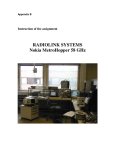
1
To our customers,
Old Company Name in Catalogs and Other Documents
On April 1st, 2010, NEC Electronics Corporation merged with Renesas Technology
Corporation, and Renesas Electronics Corporation took over all the business of both
companies. Therefore, although the old company name remains in this document, it is a valid
Renesas Electronics document. We appreciate your understanding.
Renesas Electronics website: http://www.renesas.com
April 1st, 2010
Renesas Electronics Corporation
Issued by: Renesas Electronics Corporation (http://www.renesas.com)
Send any inquiries to http://www.renesas.com/inquiry.
Notice
1.
2.
3.
4.
5.
6.
7.
All information included in this document is current as of the date this document is issued. Such information, however, is
subject to change without any prior notice. Before purchasing or using any Renesas Electronics products listed herein, please
confirm the latest product information with a Renesas Electronics sales office. Also, please pay regular and careful attention to
additional and different information to be disclosed by Renesas Electronics such as that disclosed through our website.
Renesas Electronics does not assume any liability for infringement of patents, copyrights, or other intellectual property rights
of third parties by or arising from the use of Renesas Electronics products or technical information described in this document.
No license, express, implied or otherwise, is granted hereby under any patents, copyrights or other intellectual property rights
of Renesas Electronics or others.
You should not alter, modify, copy, or otherwise misappropriate any Renesas Electronics product, whether in whole or in part.
Descriptions of circuits, software and other related information in this document are provided only to illustrate the operation of
semiconductor products and application examples. You are fully responsible for the incorporation of these circuits, software,
and information in the design of your equipment. Renesas Electronics assumes no responsibility for any losses incurred by
you or third parties arising from the use of these circuits, software, or information.
When exporting the products or technology described in this document, you should comply with the applicable export control
laws and regulations and follow the procedures required by such laws and regulations. You should not use Renesas
Electronics products or the technology described in this document for any purpose relating to military applications or use by
the military, including but not limited to the development of weapons of mass destruction. Renesas Electronics products and
technology may not be used for or incorporated into any products or systems whose manufacture, use, or sale is prohibited
under any applicable domestic or foreign laws or regulations.
Renesas Electronics has used reasonable care in preparing the information included in this document, but Renesas Electronics
does not warrant that such information is error free. Renesas Electronics assumes no liability whatsoever for any damages
incurred by you resulting from errors in or omissions from the information included herein.
Renesas Electronics products are classified according to the following three quality grades: “Standard”, “High Quality”, and
“Specific”. The recommended applications for each Renesas Electronics product depends on the product’s quality grade, as
indicated below. You must check the quality grade of each Renesas Electronics product before using it in a particular
application. You may not use any Renesas Electronics product for any application categorized as “Specific” without the prior
written consent of Renesas Electronics. Further, you may not use any Renesas Electronics product for any application for
which it is not intended without the prior written consent of Renesas Electronics. Renesas Electronics shall not be in any way
liable for any damages or losses incurred by you or third parties arising from the use of any Renesas Electronics product for an
application categorized as “Specific” or for which the product is not intended where you have failed to obtain the prior written
consent of Renesas Electronics. The quality grade of each Renesas Electronics product is “Standard” unless otherwise
expressly specified in a Renesas Electronics data sheets or data books, etc.
“Standard”:
8.
9.
10.
11.
12.
Computers; office equipment; communications equipment; test and measurement equipment; audio and visual
equipment; home electronic appliances; machine tools; personal electronic equipment; and industrial robots.
“High Quality”: Transportation equipment (automobiles, trains, ships, etc.); traffic control systems; anti-disaster systems; anticrime systems; safety equipment; and medical equipment not specifically designed for life support.
“Specific”:
Aircraft; aerospace equipment; submersible repeaters; nuclear reactor control systems; medical equipment or
systems for life support (e.g. artificial life support devices or systems), surgical implantations, or healthcare
intervention (e.g. excision, etc.), and any other applications or purposes that pose a direct threat to human life.
You should use the Renesas Electronics products described in this document within the range specified by Renesas Electronics,
especially with respect to the maximum rating, operating supply voltage range, movement power voltage range, heat radiation
characteristics, installation and other product characteristics. Renesas Electronics shall have no liability for malfunctions or
damages arising out of the use of Renesas Electronics products beyond such specified ranges.
Although Renesas Electronics endeavors to improve the quality and reliability of its products, semiconductor products have
specific characteristics such as the occurrence of failure at a certain rate and malfunctions under certain use conditions. Further,
Renesas Electronics products are not subject to radiation resistance design. Please be sure to implement safety measures to
guard them against the possibility of physical injury, and injury or damage caused by fire in the event of the failure of a
Renesas Electronics product, such as safety design for hardware and software including but not limited to redundancy, fire
control and malfunction prevention, appropriate treatment for aging degradation or any other appropriate measures. Because
the evaluation of microcomputer software alone is very difficult, please evaluate the safety of the final products or system
manufactured by you.
Please contact a Renesas Electronics sales office for details as to environmental matters such as the environmental
compatibility of each Renesas Electronics product. Please use Renesas Electronics products in compliance with all applicable
laws and regulations that regulate the inclusion or use of controlled substances, including without limitation, the EU RoHS
Directive. Renesas Electronics assumes no liability for damages or losses occurring as a result of your noncompliance with
applicable laws and regulations.
This document may not be reproduced or duplicated, in any form, in whole or in part, without prior written consent of Renesas
Electronics.
Please contact a Renesas Electronics sales office if you have any questions regarding the information contained in this
document or Renesas Electronics products, or if you have any other inquiries.
(Note 1) “Renesas Electronics” as used in this document means Renesas Electronics Corporation and also includes its majorityowned subsidiaries.
(Note 2) “Renesas Electronics product(s)” means any product developed or manufactured by or for Renesas Electronics.
Preliminary User’s Manual
QB-780822 for CAN ASSP3+
In-Circuit-Emulator
Target Device
µPD780821
µPD780822
µPD78F0822
Document No. U17172EE1V2UM00
Date Published September 2005
NEC Electronics Corporation 2005
Printed in Germany
All (other) product, brand, or trade names used in this pamphlet are the trademarks or
registered trademarks of their respective owners.
Product specifications are subject to change without notice. To ensure that you have
the latest product data, please contact your local NEC Electronics sales office.
2
Preliminary User’s Manual U17172EE1V2UM00
• The information in this document is current as of September, 2005. The information is subject to
change without notice. For actual design-in, refer to the latest publications of NEC Electronics data
sheets or data books, etc., for the most up-to-date specifications of NEC Electronics products. Not
all products and/or types are available in every country. Please check with an NEC Electronics sales
representative for availability and additional information.
• No part of this document may be copied or reproduced in any form or by any means without the prior
written consent of NEC Electronics. NEC Electronics assumes no responsibility for any errors that may
appear in this document.
• NEC Electronics does not assume any liability for infringement of patents, copyrights or other intellectual
property rights of third parties by or arising from the use of NEC Electronics products listed in this document
or any other liability arising from the use of such products. No license, express, implied or otherwise, is
granted under any patents, copyrights or other intellectual property rights of NEC Electronics or others.
• Descriptions of circuits, software and other related information in this document are provided for illustrative
purposes in semiconductor product operation and application examples. The incorporation of these
circuits, software and information in the design of a customer's equipment shall be done under the full
responsibility of the customer. NEC Electronics assumes no responsibility for any losses incurred by
customers or third parties arising from the use of these circuits, software and information.
• While NEC Electronics endeavors to enhance the quality, reliability and safety of NEC Electronics products,
customers agree and acknowledge that the possibility of defects thereof cannot be eliminated entirely. To
minimize risks of damage to property or injury (including death) to persons arising from defects in NEC
Electronics products, customers must incorporate sufficient safety measures in their design, such as
redundancy, fire-containment and anti-failure features.
• NEC Electronics products are classified into the following three quality grades: "Standard", "Special" and
"Specific".
The "Specific" quality grade applies only to NEC Electronics products developed based on a customerdesignated "quality assurance program" for a specific application. The recommended applications of an NEC
Electronics product depend on its quality grade, as indicated below. Customers must check the quality grade of
each NEC Electronics product before using it in a particular application.
"Standard": Computers, office equipment, communications equipment, test and measurement equipment, audio
and visual equipment, home electronic appliances, machine tools, personal electronic equipment
and industrial robots.
"Special": Transportation equipment (automobiles, trains, ships, etc.), traffic control systems, anti-disaster
systems, anti-crime systems, safety equipment and medical equipment (not specifically designed
for life support).
"Specific": Aircraft, aerospace equipment, submersible repeaters, nuclear reactor control systems, life
support systems and medical equipment for life support, etc.
The quality grade of NEC Electronics products is "Standard" unless otherwise expressly specified in NEC
Electronics data sheets or data books, etc. If customers wish to use NEC Electronics products in applications
not intended by NEC Electronics, they must contact an NEC Electronics sales representative in advance to
determine NEC Electronics' willingness to support a given application.
(Note)
(1) "NEC Electronics" as used in this statement means NEC Electronics Corporation and also includes its
majority-owned subsidiaries.
(2) "NEC Electronics products" means any product developed or manufactured by or for NEC Electronics (as
defined above).
M8E 02. 11-1
Preliminary User’s Manual U17172EE1V2UM00
3
Regional Information
Some information contained in this document may vary from country to country. Before using any NEC
product in your application, please contact the NEC office in your country to obtain a list of authorized
representatives and distributors. They will verify:
•
Device availability
•
Ordering information
•
Product release schedule
•
Availability of related technical literature
•
Development environment specifications (for example, specifications for third-party tools and
components, host computers, power plugs, AC supply voltages, and so forth)
•
Network requirements
In addition, trademarks, registered trademarks, export restrictions, and other legal issues may also vary
from country to country.
NEC Electronics America Inc.
Santa Clara, California
Tel: 408-588-6000
800-366-9782
Fax: 408-588-6130
800-729-9288
NEC Electronics (Europe) GmbH
Duesseldorf, Germany
Tel: 0211-65 03 1101
Fax: 0211-65 03 1327
Sucursal en España
Madrid, Spain
Tel: 091- 504 27 87
Fax: 091- 504 28 60
Succursale Française
Vélizy-Villacoublay, France
Tel: 01-30-67 58 00
Fax: 01-30-67 58 99
4
Filiale Italiana
Milano, Italy
Tel: 02-66 75 41
Fax: 02-66 75 42 99
NEC Electronics Hong Kong Ltd.
Hong Kong
Tel: 2886-9318
Fax: 2886-9022/9044
Branch The Netherlands
Eindhoven, The Netherlands
Tel: 040-244 58 45
Fax: 040-244 45 80
NEC Electronics Hong Kong Ltd.
Seoul Branch
Seoul, Korea
Tel: 02-528-0303
Fax: 02-528-4411
Branch Sweden
Taeby, Sweden
Tel: 08-63 80 820
Fax: 08-63 80 388
United Kingdom Branch
Milton Keynes, UK
Tel: 01908-691-133
Fax: 01908-670-290
NEC Electronics Singapore Pte. Ltd.
Singapore
Tel: 65-6253-8311
Fax: 65-6250-3583
NEC Electronics Taiwan Ltd.
Taipei, Taiwan
Tel: 02-2719-2377
Fax: 02-2719-5951
Preliminary User’s Manual U17172EE1V2UM00
Introduction
Target Readers
This manual is intended for users who wish to perform debugging using the
QB-780822. The readers of this manual are assumed to be familiar with the
device functions and usage, and to have knowledge of debuggers.
Purpose
This manual is intended to give users an understanding of the basic specifications and correct usage of the QB-780822.
Organization
This manual is divided into following parts.
• General
• Setup procedure
• Settings at product shipment
• Differences between target device and target interface circuit
• Cautions
• Restrictions
How to read this manual
It is assumed that the readers of this manual have general knowledge in the
fields of electrical engineering, logic circuits, and microcontrollers.
This manual describes the basic setup procedures and how to set switches.
To understand the overall functions and usages of the QB-780822
Æ Read this manual according to the CONTENTS.
To know the manipulations, command functions, and other software-related settings of the QB-780822
Æ See the user’s manual of the debugger (supplied with the QB-780822) to be
used.
Legend
Symbols and notation are used as follows:
Weight in data notation
: Left is high-order column, right is low order column
Active low notation
: xxx (pin or signal name is over-scored) or
/xxx (slash before signal name)
Memory map address:
: High order at high stage and low order at low stage
Note
: Explanation of (Note) in the text
Caution
: Item deserving extra attention
Remark
: Supplementary explanation to the text
Numeric notation
: Binary . . . XXXX or XXXB
Decimal . . . XXXX
Hexadecimal . . . XXXXH or 0x XXXX
Prefixes representing powers of 2 (address space, memory capacity)
K (kilo): 210 = 1024
M (mega): 220 = 10242 = 1,048,576
G (giga): 230 = 10243 = 1,073,741,824
Preliminary User’s Manual U17172EE1V2UM00
5
Introduction
Terminology
The meanings of the terms used in this manual are described in the table below.
Terms
Meaning
Target device
This is the device to be emulated.
Target system
This is the system to be debugged.
This includes the target program and the hardware provided by the user.
µPD78(F)0822/1
Generic name indicating µPD780821, µPD780822, µPD78F0822
Related Documents Please use the following documents in conjunction with this manual.
The related documents listed below may include preliminary versions. However,
preliminary versions are not marked as such.
Document Name
Document Number
QB-780822 In-Circuit Emulator
This manual
ID78K0-QB Ver. 2.81 Integrated Debugger
Operation
U16996E
IAR ICC78000 C Compiler
Programming Guide
ICC78000
IAR A78000 Assembler
Programming Guide
A78000
IAR XLINK
XLINK Linker and XLIB Librarian
XLINK
IAR EMbedded Workbench
Interface Guide
EW78000
Caution:
6
The related documents listed above are subject to change without notice. Be sure to
use the latest Version of each document for designing, etc.
Preliminary User’s Manual U17172EE1V2UM00
Introduction
General Precautions for Handling This Product
1.
Circumstances not covered by product guarantee
• If the product was disassembled, altered, or repaired by the customer
• If it was dropped, broken, or given another strong shock
• Use at overvoltage, use outside guaranteed temperature range, storing outside guaranteed
temperature range
• If power was turned on while the AC adapter, USB interface cable, or connection to the target
system was in an unsatisfactory state
• If the cable of the AC adapter, the USB interface cable, the emulation probe, or the like was bent
or pulled excessively
• If an AC adapter other than the supplied product was used
• If the product got wet
2.
Safety precautions
• If used for a long time, the product may become hot (50°C to 60°C). Be careful of low
temperature burns and other dangers due to the product becoming hot.
• Be careful of electrical shock. There is a danger of electrical shock if the product is used as
described above in 1 Circumstances not covered by product guarantee.
Preliminary User’s Manual U17172EE1V2UM00
7
[MEMO]
8
Preliminary User’s Manual U17172EE1V2UM00
Table of Contents
Introduction. . . . . . . . . . . . . . . . . . . . . . . . . . . . . . . . . . . . . . . . . . . . . . . . . . . . 5
Chapter 1
General . . . . . . . . . . . . . . . . . . . . . . . . . . . . . . . . . . . . . . . . . . . . . . . . . . . . . . 15
1.1
1.2
1.3
Hardware Specifications . . . . . . . . . . . . . . . . . . . . . . . . . . . . . . . . . . . . . . . . . . . . . . . . 15
System Specifications . . . . . . . . . . . . . . . . . . . . . . . . . . . . . . . . . . . . . . . . . . . . . . . . . . 17
System Configuration . . . . . . . . . . . . . . . . . . . . . . . . . . . . . . . . . . . . . . . . . . . . . . . . . . 18
1.3.1
AC adapter . . . . . . . . . . . . . . . . . . . . . . . . . . . . . . . . . . . . . . . . . . . . . . . . . . . . . 20
1.4
Package Contents . . . . . . . . . . . . . . . . . . . . . . . . . . . . . . . . . . . . . . . . . . . . . . . . . . . . . 21
Chapter 2
2.1
2.2
2.3
2.4
2.5
2.6
2.7
2.8
2.9
Setup Procedure. . . . . . . . . . . . . . . . . . . . . . . . . . . . . . . . . . . . . . . . . . . . . . . 23
Names and Functions of Hardware . . . . . . . . . . . . . . . . . . . . . . . . . . . . . . . . . . . . . . . 24
Removal of Acrylic Board . . . . . . . . . . . . . . . . . . . . . . . . . . . . . . . . . . . . . . . . . . . . . . . 27
Clock Settings . . . . . . . . . . . . . . . . . . . . . . . . . . . . . . . . . . . . . . . . . . . . . . . . . . . . . . . . 27
2.3.1
Overview of clock settings . . . . . . . . . . . . . . . . . . . . . . . . . . . . . . . . . . . . . . . . . 27
2.3.2
Clock setting methods . . . . . . . . . . . . . . . . . . . . . . . . . . . . . . . . . . . . . . . . . . . . 28
2.3.3
Main system clock . . . . . . . . . . . . . . . . . . . . . . . . . . . . . . . . . . . . . . . . . . . . . . . 29
2.3.4
Subsystem clock. . . . . . . . . . . . . . . . . . . . . . . . . . . . . . . . . . . . . . . . . . . . . . . . . 34
Software Settings. . . . . . . . . . . . . . . . . . . . . . . . . . . . . . . . . . . . . . . . . . . . . . . . . . . . . . 35
Mounting and Connecting Connectors . . . . . . . . . . . . . . . . . . . . . . . . . . . . . . . . . . . . 36
2.5.1
TET based adapter line . . . . . . . . . . . . . . . . . . . . . . . . . . . . . . . . . . . . . . . . . . . 36
2.5.2
NAIS based adapter line. . . . . . . . . . . . . . . . . . . . . . . . . . . . . . . . . . . . . . . . . . . 38
Connection of QB-780822 to Target System . . . . . . . . . . . . . . . . . . . . . . . . . . . . . . . . 40
2.6.1
Connection without using extension probe (QB-144-EP-01S) . . . . . . . . . . . . . . 40
2.6.2
Connection using extension probe (QB-144-EP-01S) . . . . . . . . . . . . . . . . . . . . 41
2.6.3
Ensuring isolation . . . . . . . . . . . . . . . . . . . . . . . . . . . . . . . . . . . . . . . . . . . . . . . . 44
2.6.4
Precautions related to emulation probe . . . . . . . . . . . . . . . . . . . . . . . . . . . . . . . 44
Power Supply and GND Pin Connection Precautions . . . . . . . . . . . . . . . . . . . . . . . . 45
Connection of USB Interface Cable and AC Adapter . . . . . . . . . . . . . . . . . . . . . . . . . 45
Switching Power On and Off. . . . . . . . . . . . . . . . . . . . . . . . . . . . . . . . . . . . . . . . . . . . . 45
Chapter 3
Chapter 4
4.1
Chapter 5
Settings at Product Shipment . . . . . . . . . . . . . . . . . . . . . . . . . . . . . . . . . . . . 47
Differences Between Target Interface Circuit and Target Device . . . . . . . 49
For µPD780822 Subseries Emulation . . . . . . . . . . . . . . . . . . . . . . . . . . . . . . . . . . . . . 50
Cautions . . . . . . . . . . . . . . . . . . . . . . . . . . . . . . . . . . . . . . . . . . . . . . . . . . . . . 53
Appendix A Notes On Target System Design. . . . . . . . . . . . . . . . . . . . . . . . . . . . . . . . . . 55
A.1
A.2
When Extension Probe Is Not Used . . . . . . . . . . . . . . . . . . . . . . . . . . . . . . . . . . . . . . . 55
When Extension Probe Is Used . . . . . . . . . . . . . . . . . . . . . . . . . . . . . . . . . . . . . . . . . . 57
Appendix B Package Drawings TET Line . . . . . . . . . . . . . . . . . . . . . . . . . . . . . . . . . . . . . 59
B.1
B.2
B.3
B.4
2.5
2.6
B.7
B.8
Target Connectors . . . . . . . . . . . . . . . . . . . . . . . . . . . . . . . . . . . . . . . . . . . . . . . . . . . . . 59
Exchange Adapters . . . . . . . . . . . . . . . . . . . . . . . . . . . . . . . . . . . . . . . . . . . . . . . . . . . . 61
YQ Connectors . . . . . . . . . . . . . . . . . . . . . . . . . . . . . . . . . . . . . . . . . . . . . . . . . . . . . . . . 62
Mount Adapters . . . . . . . . . . . . . . . . . . . . . . . . . . . . . . . . . . . . . . . . . . . . . . . . . . . . . . . 64
Check Pin Adapter . . . . . . . . . . . . . . . . . . . . . . . . . . . . . . . . . . . . . . . . . . . . . . . . . . . . . 66
Spacer Adapters . . . . . . . . . . . . . . . . . . . . . . . . . . . . . . . . . . . . . . . . . . . . . . . . . . . . . . 67
Emulation Probe . . . . . . . . . . . . . . . . . . . . . . . . . . . . . . . . . . . . . . . . . . . . . . . . . . . . . . 69
Clock Board . . . . . . . . . . . . . . . . . . . . . . . . . . . . . . . . . . . . . . . . . . . . . . . . . . . . . . . . . . 70
Preliminary User’s Manual U17172EE1V2UM00
9
Appendix C Package Drawings NAIS Line . . . . . . . . . . . . . . . . . . . . . . . . . . . . . . . . . . . . 71
C.1
C.2
C.3
C.4
C.5
C.6
C.7
Target Connectors . . . . . . . . . . . . . . . . . . . . . . . . . . . . . . . . . . . . . . . . . . . . . . . . . . . . . 71
Exchange Adapters . . . . . . . . . . . . . . . . . . . . . . . . . . . . . . . . . . . . . . . . . . . . . . . . . . . . 73
Mount Adapters . . . . . . . . . . . . . . . . . . . . . . . . . . . . . . . . . . . . . . . . . . . . . . . . . . . . . . . 74
Check Pin Adapter . . . . . . . . . . . . . . . . . . . . . . . . . . . . . . . . . . . . . . . . . . . . . . . . . . . . . 75
Spacer Adapters. . . . . . . . . . . . . . . . . . . . . . . . . . . . . . . . . . . . . . . . . . . . . . . . . . . . . . . 76
Emulation Probe. . . . . . . . . . . . . . . . . . . . . . . . . . . . . . . . . . . . . . . . . . . . . . . . . . . . . . . 77
Clock Board . . . . . . . . . . . . . . . . . . . . . . . . . . . . . . . . . . . . . . . . . . . . . . . . . . . . . . . . . . 78
Appendix D Target Interface Definition. . . . . . . . . . . . . . . . . . . . . . . . . . . . . . . . . . . . . . . 79
10
Preliminary User’s Manual U17172EE1V2UM00
List of Figures
Figure 1-1:
Figure 1-2:
Figure 2-1:
Figure 2-2:
Figure 2-3:
Figure 2-4:
Figure 2-5:
Figure 2-6:
Figure 2-7:
Figure 2-8:
Figure 2-9:
Figure 2-10:
Figure 2-11:
Figure 2-12:
Figure 2-13:
Figure 2-14:
Figure 2-15:
Figure 2-16:
Figure 2-17:
Figure 2-18:
Figure 4-1:
Figure A-1:
Figure A-2:
Figure A-3:
Figure A-4:
Figure B-1:
Figure B-2:
Figure B-3:
Figure B-4:
Figure B-5:
Figure B-6:
Figure B-7:
Figure B-8:
Figure B-9:
Figure B-10:
Figure B-11:
Figure B-12:
Figure B-13:
Figure C-1:
Figure C-2:
Figure C-3:
Figure C-4:
Figure C-5:
Figure C-6:
Figure C-7:
Figure C-8:
Figure C-9:
Figure C-10:
Figure C-11:
QB-780822 .................................................................................................................. 16
System Configuration .................................................................................................. 18
Names of Parts of QB-780822 .................................................................................... 24
Clock Board ................................................................................................................. 25
Acrylic Board Removal Method ................................................................................... 27
Oscillator (Main System Clock) ................................................................................... 29
Mapping of Oscillator to Main Clock Type I (Main System Clock)............................... 29
Resonator (Main System Clock: 3-Pin) ....................................................................... 30
Connection to Main Clock Type II (Main System Clock: 3-Pin) ................................... 31
Resonator (Main System Clock: 2-Pin) ....................................................................... 32
Connection to Main Clock Type II (Main System Clock: 2-Pin) ................................... 33
Connection to Sub Clock Type I (Subsystem Clock)................................................... 34
TC Projection Diagram ................................................................................................ 38
How to Insert/Remove EA and TC .............................................................................. 39
Connection without using Extension Probe ................................................................. 40
How to use Probe Holder ............................................................................................ 41
Connection of GND Lines............................................................................................ 42
Location at which GND Line can be connected .......................................................... 43
Connection Using Emulation Probe ............................................................................ 44
Connector Positions .................................................................................................... 45
Emulation Circuit Equivalent Circuit 1 (1/2) ................................................................. 51
For 100-pin GC package ............................................................................................. 55
For 100-pin GF package ............................................................................................. 56
For 100-pin GC package ............................................................................................. 57
For 100-pin GF package ............................................................................................. 58
Target Connector for 100-pin QFP GC-package......................................................... 59
Target Connector for 100-pin QFP GF-package ......................................................... 60
Exchange Adapter for 100-pin QFP GC-package ....................................................... 61
Exchange Adapter for 100-pin QFP GF-package ....................................................... 61
YQ Connector for 100-pin QFP GC-package .............................................................. 62
YQ Connector for 100-pin QFP GF-package .............................................................. 63
Mount Adapter for 100-pin QFP GC-package ............................................................. 64
Mount Adapter for 100-pin QFP GF-package ............................................................. 65
Check Pin Adapter 144-pin QFP ................................................................................. 66
Spacer Adapter for 100-pin QFP GC-package............................................................ 67
Spacer Adapter for 100-pin QFP GF-package ............................................................ 68
Emulation Probe 144-pin ............................................................................................. 69
Clock Board ................................................................................................................. 70
Target Connector for 100-pin QFP GC-package......................................................... 71
Target Connector for 100-pin QFP GF-package ......................................................... 72
Exchange Adapter for 100-pin QFP GC-package ....................................................... 73
Exchange Adapter for 100-pin QFP GF-package ....................................................... 73
Mount Adapter for 100-pin QFP GC-package ............................................................. 74
Mount Adapter for 100-pin QFP GF-package ............................................................. 74
Check Pin Adapter 100-pin QFP ................................................................................. 75
Spacer Adapter for 100-pin QFP GC-package............................................................ 76
Spacer Adapter for 100-pin QFP GF-package ............................................................ 76
Emulation Probe 144-pin ............................................................................................. 77
Clock Board ................................................................................................................. 78
Preliminary User’s Manual U17172EE1V2UM00
11
12
Preliminary User’s Manual U17172EE1V2UM00
List of Tables
Table 1-1:
Table 1-2:
Table 1-3:
Table 1-4:
Table 1-5:
Table 1-6:
Table 1-7:
Table 1-8:
Table 1-9:
Table 1-10:
Table 2-1:
Table 2-2:
Table 3-1:
QB-780822 Hardware Specifications ............................................................................. 15
QB-780822 System Specifications ................................................................................. 17
Devices Subject to Emulation by QB-780822................................................................. 18
Check Pin Adapters........................................................................................................ 19
Exchange Adapters ........................................................................................................ 19
Emulation Probes ........................................................................................................... 19
YQ Connectors ............................................................................................................... 20
Spacer Adapters............................................................................................................. 20
Target Connectors.......................................................................................................... 20
Mount Adapters .............................................................................................................. 20
Hardware Settings When Setting Main System Clock.................................................... 28
Hardware Settings When Setting Subsystem Clock....................................................... 28
Settings at Shipment ...................................................................................................... 47
Preliminary User’s Manual U17172EE1V2UM00
13
14
Preliminary User’s Manual U17172EE1V2UM00
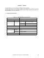
Chapter 1
General
The QB-780822 is an in-circuit emulator for emulating the µPD78(F)0822/1.
Hardware and software can be debugged efficiently in the development of systems in which the
µPD78(F)0822/1 is used. This manual descries basic setup procedures, hardware specifications, system specifications, and how to set switches.
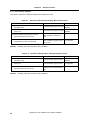
1.1 Hardware Specifications
Table 1-1:
QB-780822 Hardware Specifications
Parameter
Target device
Specification
µPD78(F)0822/1
Operating voltage
µPD78(F)0822/1
Operating frequency
µPD78(F)0822/1
4.0 to 5.5 V
Main system
clock
VDD = 4.0 to 5.5 V: 16 MHz
Subsystem clock
VDD = 4.0 to 5.5 V: 32.768 kHz
Ring clock
VDD = 4.0 to 5.5 V: 240 kHz (Typ.)
Operating temperature range
0 to 40°C (No condensation)
Storage temperature range
-15 to 60°C (No condensation)
External dimensions
See figure below
Power consumption
AC adapter for
QB-780822
15 V, 1 A
Target system
power supply
Same level as target device. Deviations based on emulation structure possible.
Weight
382 g
Host interface
USB interface (1.1, 2.0)
Preliminary User’s Manual U17172EE1V2UM00
15
Chapter 1
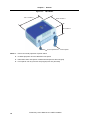
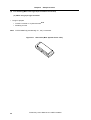
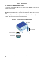
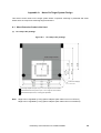
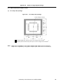
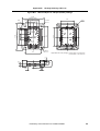
Figure 1-1:
General
QB-780822
112.7 mmNote 1
84.6 mmNote 2
58 mmNote 3
Front spacerNote 4
Rear spacer
Notes: 1. Does not include projection of power switch
2. Includes projection of screw that fixes rear spacer
3. Dimension when rear spacer is made shortest (88 mm when longest)
4. Front spacer can vary from 20 mm (longest) to 5 mm (shortest)
16
Preliminary User’s Manual U17172EE1V2UM00
Chapter 1
General
1.2 System Specifications
This section shows the QB-780822 system specifications.
Table 1-2:
QB-780822 System Specifications
Parameter
Program execution
functions
Break functions
Trace functions
Real-time execution function
Go, Start from Here, Go & Go, Come Here, Restart, Return
Out, Ignore break points and Go
Non-real-time execution
function
Step execution
Event break
Execution: 8 points
Access: Byte 8 points, word 2 points
Software break
2000 points
Pre-execution break
16 points
Fail-safe break
Exists
Other
Forcible break, trace full break, trace delay break, time-out
break, timer overflow break
Trace data types
Program address, program data, access address, access
data, status
Trace modes
Full trace, section trace, qualify trace
Trace functions
Delay function, full stop function
Memory capacity
128 K frames
Real-time RAM monitoring function
Time measurement functions
Other functions
Specification
All spaces
Measurement clock
50 MHz or CPU clock
Measurement objects
Beginning through end of program execution
Start event through end event
Maximum measurement
time
Approximately 24 hours (Resolution 41 µs)
Minimum resolution
20 ns (Measurement time: 85 seconds)
Number of timers for measurement
Start through end of program execution: 1
Start event through end event: 2
Measurement results
Maximum, minimum, average, cumulative, number of
passes (between events)
Other
Timer overflow break function,
time-out break function
Mapping function, event function, coverage function, snapshot function, DMM function, stub function, power-off emulation function, pin mask function
Preliminary User’s Manual U17172EE1V2UM00
17
Chapter 1
General
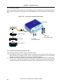
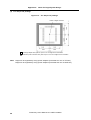
1.3 System Configuration
This section shows the system configuration when using the QB-780822 connected to a PC
(PC-9821 series, PC/ATTM compatible). Connection is possible even without optional products.
Table 1-3:
Series Name
(Common Name)
CANASSP3+ Series
Devices Subject to Emulation by QB-780822
Device Name
Package
Flash Memory Version
100-pin QFP (GC, GF)
Figure 1-2:
Mask ROM Version
µPD780822,
µPD780821
µPD78F0822
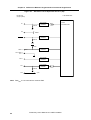
System Configuration
<1>
<3>
<5>
<4>
<2>
<6a>
<7>
<8>
<8>
<9>
TET-line
NAIS-line
<6b>
<12>
<12>
<10>
<11>
<1>
<2>
<3>
<4>
<5>
18
Host machine:
D78K0-QB Disk/Accessory Disk:Note1
USB interface cable:
AC adapter:
QB-780822:
<9>
<11>
PC-9821 series, PC/AT compatible can be used
Debugger, USB drivers, manual, device files etc.
Cable connecting QB-780822 to host machine
Can support 100 to 240 V by replacing AC plug
This product
Preliminary User’s Manual U17172EE1V2UM00
Chapter 1
<6a, 6b> Check pin adapter:
<7> Emulation probe:
<8> Exchange adapter:
<9> Spacer adapter:
<10> YQ connector:
<11> Target connector:
<12> Mount adapter:
General
Adapter used when observing waveforms on oscilloscope
Flexible type of emulation probe
Adapter that performs pin conversion
Adapter for height regulation
Connector that connects exchange adapter to target connector
Connector soldered to target system
Adapter for socket mounting target device
Notes: 1. Obtain these items from the NEC Electronics website.
http://www.ee.nec.de/products/micro/
2. Refer to 1.4 ”Package Contents” on page 21 for the purchase forms of the above
products.
3. Position <6> to <12> must be ordered separately,
where positions <6>, <8>, <10> and <11> are mandatory
where positions <7>, <9> and <12> are optional
for target interface connection.
4. There are two adapter lines available. One is based on the TET-line connectors, one is
based on the NAIS-line connectors. For ordering refer to tables 1-4 to 1-10 for the correct
order codes for each line (TET, NAIS connector vendor).
Caution:
The two adapter-lines could not mixed up.
Table 1-4:
Check Pin Adapters
Package
Check Pin Adapter
TET-Line
Check Pin Adapter
NAIS-Line
Common
QB-144GA-01
QB-100GC-CA-01S
Common
QB-144CA-01
QB-100GF-CA-01S
Table 1-5:
Exchange Adapters
Package
Exchange Adapter
TET-Line
Exchange Adapter
NAIS-Line
100GC
QB-100GC-EA-02T
QB-100GC-EA-02S
100GF
QB-100GF-EA-02T
QB-100GF-EA-02S
Table 1-6:
Emulation Probes
Package
Emulation Probe (both lines)
Common
QB-144-EP-01S
Preliminary User’s Manual U17172EE1V2UM00
19
Chapter 1
Table 1-7:
General
YQ Connectors
Package
YQ Connector
TET-Line
YQ Connector
NAIS-Line
100GC
QB-100GC-YQ-01T
not required
100GF
QB-100GF-YQ-01T
not required
Table 1-8:
Spacer Adapters
Package
Spacer Adapter
TET-Line
Spacer Adapter
NAIS-Line
100GC
QB-100GC-YS-01T
QB-100GC-SA-01S
100GF
QB-100GF-YS-01T
QB-100GF-SA-01S
Table 1-9:
Target Connectors
Package
Target Connector
TET-Line
Target Connector
NAIS-Line
100GC
QB-100GC-NQ-01T
QB-100GC-TC-01S
100GF
QB-100GF-NQ-01T
QB-100GF-TC-01S
Table 1-10:
Mount Adapters
Package
Target Connector
TET-Line
Target Connector
NAIS-Line
100GC
QB-100GC-HQ-01T
QB-100GC-MA-01S
100GF
QB-100GF-HQ-01T
QB-100GF-MS-01S
1.3.1 AC adapter
By replacing the AC plug, this product can support 100 to 240 V.
The following three types are included.
20
Preliminary User’s Manual U17172EE1V2UM00
Chapter 1
General
1.4 Package Contents
The following items have been placed in the QB-780822 packing box. Please check the contents.
Products supplied with QB-780822
1: QB-780822
2: AC adapter
3: USB interface cable
4: Clock board set
•
•
•
•
•
5:
6:
7:
8:
Main Clock Type I
Main Clock Type II
Main Clock Type III (Mounted at shipment)
Sub Clock Type I
Sub Clock Type II (Mounted at shipment)
List of Contents
Readme
CE certification
PG-FPL
The following products are sold as single items.
• Emulation probe
• Exchange adapter
• YQ connector
• Target connector
• Check pin adapter
• Spacer adapter
• Mount adapter
Preliminary User’s Manual U17172EE1V2UM00
21
[MEMO]
22
Preliminary User’s Manual U17172EE1V2UM00
Chapter 2 Setup Procedure
This chapter explains the QB-780822 setup procedure.
Setup can be completed by performing installation setup in the order in which it appears in this chapter.
Perform setup along the lines of the following procedure.
See 2.1 ”Names and Functions of Hardware” on page 24 for clock board positions.
(1)
Clock settings
The internal clock board is mounted at shipment.
If using the internal clock, modifications of the settings are unnecessary.
If modification is necessary, see 2.2 ”Removal of Acrylic Board” on page 27 and 2.3 ”Clock
Settings” on page 27.
(2)
Software settings
See 2.4 ”Software Settings” on page 35.
(3)
Mounting and connecting connectors
See 2.5 ”Mounting and Connecting Connectors” on page 36.
(4)
Connection of QB-780822 for µPD78(F)0822/1 to target system
See 2.6 ”Connection of QB-780822 to Target System” on page 40.
(5)
Connecting USB interface cable and AC adapter
See 2.8 ”Connection of USB Interface Cable and AC Adapter” on page 45.
(6)
Switching power On and Off
See 2.9 ”Switching Power On and Off” on page 45.
Preliminary User’s Manual U17172EE1V2UM00
23
Chapter 2
Setup Procedure
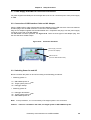
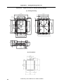
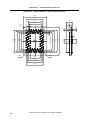
2.1 Names and Functions of Hardware
Figure 2-1:
Names of Parts of QB-780822
Top View
Bottom View
Sub Clock Type II
SubClockTypeII
Main Clock Type III
Main Clock Type III
Power switch
CN5
CN6
POWER
TARGET
TCN2 TCN3 TCN1
Side View
Power supply connector
USB connector
24
Preliminary User’s Manual U17172EE1V2UM00
Chapter 2
Setup Procedure
Figure 2-2:
S3
C1
S2
Clock Board
Main Clock Type II
C2
Main Clock Type III
S1
OSC1
Main Clock Type I
S4
S6
S5
C2'
C1'
8
1
8
OSC1'
1
Main Clock Type I
Main Clock Type II
C1
8
1
Main Clock Type III
C2
OSC1
Sub Clock Type II
C2'
C1'
OSC1'
Sub
1
Clock Type
I 5
Sub Clock Type I
(1)
5
1
Sub Clock Type II
TCN1, TCN2
These are connectors for connecting a check pin adapter or emulation probe.
(2)
CN5
CN5 (Main clock board connector) is the connector for mounting the main clock board. Main Clock
Type III is mounted at shipment.
(3)
CN6
CN6 (Subclock board connector) is the connector for mounting the subclock board.
Sub Clock Type II is mounted at shipment.
(4)
POWER (Red LED)
This is an LED that shows whether or not the power supply of the QB-780822 is switched on.
LED State
(5)
QB-780822 State
Lit
Power switch ON
Not lit
Power switch OFF or AC adapter not connected to QB-780822
Blinking
Internal error occurred (Contact an NEC Electronics sales representative or distributor)
TARGET (Green LED)
This is an LED that shows whether or not the power supply of the target system is switched on.
Preliminary User’s Manual U17172EE1V2UM00
25
Chapter 2
Setup Procedure
LED State
(6)
Target System State
Lit
Target system power supply ON
Not lit
Target system power supply OFF or target system not connected
Power switch
This is the power switch of the QB-780822.
It is OFF at shipment.
26
Preliminary User’s Manual U17172EE1V2UM00
Chapter 2
Setup Procedure
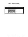
2.2 Removal of Acrylic Board
To modify the clock setup, the acrylic board on the bottom of the QB-780822 must be removed.
The acrylic board can be removed by lifting it up.
Figure 2-3:
Acrylic Board Removal Method
2.3 Clock Settings
2.3.1 Overview of clock settings
The following 7 types of clock settings are available.
For details, see 2.3.2 Clock setting methods.
(1)
Main system clock
(1) Mount the clock board in CN5 and use the internally generated clock
(2) Mount the clock board in CN5 and use an externally input clock
(3) Mount the oscillator clock board in CN5 and generate the clock from the clock board
(4) Mount the oscillation circuit clock board in CN5 and generate the clock from the clock board
(2)
Subsystem clock
(1) Mount the clock board in CN6 and use the internally generated clock
(2) Mount the clock board in CN6 and use an externally input clock
(3) Mount the oscillation circuit clock board in CN6 and generate the clock from the clock board
Preliminary User’s Manual U17172EE1V2UM00
27
Chapter 2
Setup Procedure
2.3.2 Clock setting methods
This section shows the hardware settings when setting the clock.
Table 2-1:
Hardware Settings When Setting Main System Clock
Type of Clock to Use
CN5
(1) Mount clock board in CN5 and use internally
generated clock
Mount Main Clock Type III in CN5
Mounted in CN5 at
shipment
(2) Mount clock board in CN5 and use internally
input clock
Mount Main Clock Type III in CN5
Mounted in CN5 at
shipment
(3) Mount oscillator clock board in CN5 and
generate clock from clock board
Mount Main Clock Type I on
which oscillator is mounted in
CN5
(4) Mount oscillation circuit clock board in CN5
and generate clock from clock board
Mount Main Clock Type II on
which oscillation circuit is assembled in CN5
Remark:
not supported
Settings other than the above are prohibited.
Table 2-2:
Hardware Settings When Setting Subsystem Clock
Type of Clock to Use
CN6
Remarks
(1) Mount clock board in CN6 and use internally
generated clock
Mount Sub Clock Type II in CN6
Mounted in CN6 at
shipment
(2) Mount clock board in CN6 and use internally
input clock
Mount Sub Clock Type II in CN6
not supported
(3) Mount oscillator clock board in CN6 and
generate clock from clock board
Mount Sub Clock Type I on which
oscillation circuit is assembled in
CN6
Remark:
28
Remarks
Settings other than the above are prohibited.
Preliminary User’s Manual U17172EE1V2UM00
Chapter 2
Setup Procedure
2.3.3 Main system clock
(1)
•
For mounting Main Clock Type I (for oscillator use)
Things to prepare
• Oscillator (with pins as shown in Figure 2-4 and 5 V power supply)
Figure 2-4:
NC
Oscillator (Main System Clock)
VCC
VCC
NC
GND
GND
CLOCK OUT
CLOCK OUT
<Procedure>
<1> Prepare the QB-780822 and Main Clock Type I. Remove the clock board that is mounted in the
CN5 socket on the QB-780822.
When removing the clock board, do so carefully, since the pins of the CN5 socket bend easily.
<2> Implement the prepared oscillator in Main Clock Type I. Carefully insert it in the direction of the
number 1 pin mark.
Figure 2-5:
Mapping of Oscillator to Main Clock Type I (Main System Clock)
Socket
VCC
Oscillator Pin
S6
NC
S1
8
Crystal oscillator
S5
GND
Clock out
S4
Vcc
S1
S2
S3
S4
S5
S6
1
CLOCK OUT
Main Clock Type I
GND
S3
S2
NC
Board Pin Number
<3> Fit Main Clock Type I prepared in <2> in the CN5 socket from which the clock board was removed
in <1>.
In the debugger, only the "Clock Board" button can be selected (others displayed in gray) at this time.
For the frequency at this time, the clock of the oscillator that is mounted on the clock board is used.
Preliminary User’s Manual U17172EE1V2UM00
29
Chapter 2
(2)
Setup Procedure
For mounting Main Clock Type II (for oscillation circuit use)
(a) When using 3-pin type resonator
•
Things to prepare
• Ceramic resonator or crystal resonatorNote
• Soldering tool set
Note: CSTCE10M0G (by Murata Mfg. Co., Ltd.) is assumed.
Figure 2-6:
30
Resonator (Main System Clock: 3-Pin)
Preliminary User’s Manual U17172EE1V2UM00
Chapter 2
Setup Procedure
<Procedure>
<1> Prepare the QB-780822 and Main Clock Type II. Remove the clock board that is mounted in the
CN5 socket on the QB-780822.
When removing the clock board, do so carefully, since the pins of the CN5 socket bend easily.
<2> Solder the ceramic resonator or crystal resonator used in OSC1 of Main Clock Type II.
Figure 2-7:
Connection to Main Clock Type II (Main System Clock: 3-Pin)
Main Clock Type II (Back)
8
Pin Number
OSC2
Pin 3
Connection
Ceramic resonator or crystal resonator
CN2
NEC JAPAN
OSC2
Pin 2
Pin 1
1
For pad type
Circuit Diagram
X2
X1
3
OSC1
1
2
<3> Fit Main Clock Type II of <2> in the CN5 socket from which the clock board was removed in <1>.
Preliminary User’s Manual U17172EE1V2UM00
31
Chapter 2
Setup Procedure
(b) When using 2-pin type resonator
•
Things to prepare
• Ceramic resonator or crystal resonator
• Capacitor C1
• Capacitor C2
• Soldering tool set
Figure 2-8:
Resonator (Main System Clock: 2-Pin)
<Procedure>
<1> Prepare the QB-780822 and Main Clock Type II. Remove the clock board that is mounted in the
CN5 socket on the QB-780822.
When removing the clock board, do so carefully, since the pins of the CN5 socket bend easily.
<2> Solder the ceramic resonator or crystal resonator used in OSC1 of Main Clock Type II and capacitor C1 and capacitor C2 conforming with its oscillation frequency as follows. When soldering, use
either through-hole types or pad types.
32
Preliminary User’s Manual U17172EE1V2UM00
Chapter 2
Figure 2-9:
Setup Procedure
Connection to Main Clock Type II (Main System Clock: 2-Pin)
Main Clock Type II
1
C1
Pin Number
Connection
OSC1
OSC1'
C2'
Main Clock Type II
C1'
C1, C1'
Capacitor C1
C2, C2'
Capacitor C2
OSC1, OSC1' Ceramic resonator or crystal resonator
C2
8
For through-hole type
For pad type
Circuit Diagram
X2
X1
C2
C1
<3> Fit Main Clock Type II of <2> in the CN5 socket from which the clock board was removed in <1>.
In the debugger, only the "Clock Board" button can be selected at this time (others are displayed in
gray). For the frequency at this time, the clock of the oscillation circuit that is mounted on the clock
board is used.
(3)
For mounting Main Clock Type III (for internally generated clock or externally input clock
use)
Main Clock Type III is fitted in the CN5 socket at shipment. If in the same state as at shipment,
hardware settings are unnecessary.
In the debugger, only "External Clock" or "System Clock" can be selected at this time ("Clock
Board" is displayed in gray). If "External Clock" is selected, a clock that is input from the target system is used. If "System Clock" is selected, select the desired frequency from the dialog menu.
If inputting an external clock, input a square wave of the same potential as the target device in the
clock pin (X1, XT1) (input of inverse waveform to X2, XT2 is unnecessary).
Preliminary User’s Manual U17172EE1V2UM00
33
Chapter 2
Setup Procedure
2.3.4 Subsystem clock
(1)
•
For mounting Sub Clock Type I (For oscillation circuit use)
Things to prepare
• Ceramic resonator or crystal resonatorNote
• Capacitor C1
• Capacitor C2
• Soldering tool set
Note: The resonator used is assumed to be NC-206 (by Kyushu Dentsu Co., Ltd.).
<Procedure>
<1> Prepare the QB-780822 and Sub Clock Type I. Remove the clock board that is mounted in the
CN6 socket on the QB-780822.
When removing the clock board, do so carefully, since the pins of the CN6 socket bend easily.
<2> Solder the ceramic resonator or crystal resonator that is used in Sub Clock Type- and capacitor C1
and capacitor C2 that conform to its oscillation frequency as follows.
Figure 2-10:
Connection to Sub Clock Type I (Subsystem Clock)
Sub Clock Type I
C1
OSC1
Clock Type
OSC1'
C1'
Sub
1
Pin Number
Connection
C1, C1'
Capacitor C1
C2, C2'
Capacitor C2
C2'
I 5
C2
OSC1, OSC1' Ceramic resonator or crystal resonator
For pad type
For through-hole type
Circuit Diagram
470 kΩ
C1(C1')
NC-206
3
4
1
XT1
1
2
VCC
6
3
IC2
4
Vcc
5
GND 2
SN74LVC2G04DCK
C2(C2')
10 MΩ
Remark:
Places surrounded by broken lines indicate portions installed on the parts board.
<3> Fit Sub Clock Type I of <2> in the CN6 socket from which the clock board was removed in <1>.
In the debugger, only the "Clock Board" button can be selected at this time (others are displayed in
gray). For the frequency at this time, the clock of the oscillation circuit that is mounted on the clock
board is used.
34
Preliminary User’s Manual U17172EE1V2UM00
Chapter 2
(2)
Setup Procedure
For mounting Sub Clock Type II (for internally generated clock or externally input clock
use)
Sub Clock Type II is fitted in the CN6 socket at shipment. If in the same state as at shipment,
hardware settings are unnecessary.
In the debugger, only "External Clock" or "System Clock" can be selected at this time ("Clock
Board" is displayed in gray). If "External Clock" is selected, a clock that is input from the target system is used. If "System Clock" is selected, select the desired frequency from the dialog menu.
If inputting an external clock, input a square wave of the same potential as the target device to the
clock pin (X1, XT1) (input of inverse waveform to X2, XT2 is unnecessary).
2.4 Software Settings
For details, see the ID78K0-QB Ver. 2.81 Integrated Debugger Operation User's Manual (U16996E).
Preliminary User’s Manual U17172EE1V2UM00
35
Chapter 2
Setup Procedure
2.5 Mounting and Connecting Connectors
This section describes the methods of connecting the QB-780822 and target system.
Make connections with both the QB-780822 and target system powered OFF.
The following abbreviations are used in this section.Note
• NQ: (TC) Target connector
• YQ: (--) YQ connector
• EA: (EA) Exchange adapter
• HQ: (MA) Mount adapter
• CA: (CA) Check pin adapter
• YS: (SA) Spacer adapter
Note: For TET based adapter line see chapter 2.5.1
For NAIS based adapter line see chapter 2.5.2
2.5.1 TET based adapter line
(1)
Mounting NQ in target system
<1> Thinly apply a two-component epoxy adhesive (hardening time at least 30 minutes) to the
ends of the four projections on the base of the NQ and adhere the NQ to the user board
(clean the surface of the user board using alcohol or the like). If alignment of user board
pads to NQ leads is difficult, align them as in (2).
<2> Align by inserting the guide pins for alignment for the NQ (NQ-Guide) through the pin holes
on the top of the NQ. Accessory holes are ö1.0 mm non-through holes in 2 or 3 places.
(For hole positions, see the particular NQ drawing.)
<3> Solder after fitting the HQ to the NQ. This is to prevent troubles such as flux or solder splashing and adhering to the NQ contact pins when soldering.
Soldering conditions
Caution:
Solder reflow
240°C × 20 seconds or less
Manual soldering
240°C ×10 seconds or less (1 pin)
Do not perform washing by flux immersion or vapor.
<4> Take away the guide pins.
(2)
Mounting YQ on NQ
<1> After confirming that there are no broken or bent YQ contact pins, fit the YQ in the NQ and
fasten the screw. If repeatedly inserting and removing, be sure to inspect the YQ pins before
fitting. If pins are bent, correct them using something thin and flat such as the edge of a
knife.
<2> Accessory holes are needed in prescribed positions in 4 places in the board for connecting
the YQ. Fasten the YQ to the NQ on the user board using the supplied M2 × 10 mm screws.
The thickness of a board corresponding to these screws is 1.0 to 2.0 mm. Fasten the screws
equally in the four corners using a No. 1 or No. 0 precision (+) driver or torque driver. The
tightening torque of the screws is 0.55kg • f • cm (0.054N • m) Max. Too great tightening
causes bad connections.
Screws for fitting to the NQ (M2 × 10 mm/4) are included with the YQ.
36
Preliminary User’s Manual U17172EE1V2UM00
Chapter 2
(3)
Setup Procedure
Plugging EA into YQ
Match the No. 1 pin position of the YQ or YS (C cuts match in both) to the No. 1 pin position of the
EA and plug in.
• When plugging or unplugging, press on the NQ, YQ, and YS with a finger so that there is no
force on the NQ.
• When plugging or unplugging, be careful of the direction of rocking.
As a tool when unplugging, insert a bamboo skewer or the like between the YQ (YS) and EA and
rock while slowly unplugging. Be careful since the connector will be damaged if this is done in the
wrong direction.
(4)
Precautions for handling NQ, YQ, YS
<1> When taking the NQ from the box, press down on the body and take out the sponge first.
<2> Since the pins of the YQ are thin and easily bent, be careful. When inserting it in the NQ,
confirm that there are no bent pins.
<3> When screwing a YQ soldered to a board to the NQ, fasten the screws in four places in turn
using a No. 0 or No. 1 (+) precision driver or torque driver after tentatively tightening them.
Fix the torque at 0.054 Nm (Max.). If just one place is overtightened, it may cause poor contact. Moreover, a board being connected to the YQ must have accessory holes in prescribed
positions (4 places: φ2.3 mm or φ3.3 mm). The φ3.8 mm or φ4.3 mm that is the screw head
size is an area where wiring is prohibited.
<4> In YQ and YS removal, since there is a danger of YQ pins being bent or broken when prying
and rocking, remove them gradually using a (−) driver from four directions. Moreover, to connect and use the YQ and YS, screw the YQ to the NQ according to the YQGUIDE (sold separately) using a 2.3 mm (−) driver and then connect it to the YS. Fix the torque at 0.054 Nm
(Max.). If even one place is overtightened, it may cause poor contact.
<5> For the NQ, YQ, and YS, since there is a danger that washing fluid on the structure will
remain in the connector, do not perform washing.
<6> NQ, IC, and YQ cannot be used in combination.
<7> An NQ/YQ system cannot be used in an environment of vibrations or shocks.
<8> It is assumed that this product will be used in system development and evaluation. Moreover,
when used in Japan, Electrical Appliance and Material Control Law and electromagnetic disturbance countermeasures have not been applied.
<9> Since there are rare cases of shape change if the box is left for a long time in a place where
it is 50°C or higher, for safekeeping, store it in a place where it is no higher than 40°C and
direct sunlight does not hit it.
<10> For details about handling the NQ, YQ, and YS, see the NQPACK series technical materials
at the website of Tokyo Eletech Corporation.
Tokyo Eletech Corporation website: http://www.tetc.co.jp/
Preliminary User’s Manual U17172EE1V2UM00
37
Chapter 2
(5)
Setup Procedure
Precautions on mounting NQ and IC
<1> Confirm that there is no weld flash in the resin (sealant part) of the IC. If there is weld flash,
remove it using a knife or the like.
<2> Confirm that there is no weld flash breaking or bending of IC leads. In particular, confirm the
planarity of IC leads. If there is abnormality in the planarity, correct that portion.
<3> Viewing the NQ contact pins from the top, if there are foreign bodies on them, remove them
using a brush or the like.
After confirming (1) to (3), fit the IC to the NQ. Also fit the HQ.
<4> Put the supplied M2 × 6 mm screws in the 4 accessory holes of the HQ and fasten the
screws in opposite corners. At that time, use either the dedicated screw driver that is supplied or a torque driver to fasten them equally in turn with a tightening torque of MAX.
0.55 kg • f (0.054 Nm). Since the contact is poor if tightening is too great, once you have
lightly fastened the HQ screws, tighten them again.
<5> Depending on the use environment, when starting up a device that has been left for a long
time, starting it may be difficult. In this case, loosen the screws slightly and then retighten
them.
<6> If startup still is difficult after (5) above, check (1) to (3) again.
<7> Tightening the screws of the HQ too much may give rise to cracks in the moulded part of the
HQ (plastic part) and bend the mould into a bowed shape, making contact poor.
<8> After soldering the NQ, do not perform washing by flux immersion or vapour.
2.5.2 NAIS based adapter line
(1)
Mounting target connector (TC) on target system
<1> Apply cream solder to the foot pattern for mounting the IC on the target system.
<2> TC has a cylindrical projection in the center of the underside (Figure 2-11). Apply a two-component hardening type epoxy adhesive agent (a type that hardens in 15 to 30 minutes) sparingly to the underside of the projection to temporarily secure the connector at the specified
location on the target system. Make sure that the position of pin 1 of the connector (where
the corner is cut) matches the position of pin 1 on the target board.
<3> TC mounting conditions
(a) To mount TC by reflow: 245°C × 20 seconds max. (heating)
(b) To mount TC by manual soldering: 320°C × 5 seconds max. (per pin)
Figure 2-11:
TC Projection Diagram
<4> Note on flux splashing
The flux splashing that takes place while the connector is being mounted often results in
defective conduction. Be sure to cover the upper part of the connector with aluminium foil.
Caution:
38
Do not clean the flux because the structure of the connector easily allows cleaner to
enter.
Preliminary User’s Manual U17172EE1V2UM00
Chapter 2
(2)
Setup Procedure
Inserting exchange adapter (EA) in TC
<1> Insert EA, MA, CA, or SA in target connector (TC) so that the position of pin 1 (where the
corner is cut) on each board matches.
(a) When TC is inserted or removed, hold TC with your fingers so that no excessive force is
applied to the connector.
(b) Remove or insert the adapter in the correct direction. (Figure 2-12)
Use a bamboo spit or similar object as a tool to remove the connector. Insert the tool between
TC and EA and remove TC in the correction direction as shown in Figure 2-12. If force is
applied
to the connector in the wrong direction, the connector will be damaged.
Figure 2-12:
(3)
How to Insert/Remove EA and TC
General cautions on using TC, EA, MA, CA, and SA
<1> Causes of faulty contact of connector
(a) If flux gets inside TC when it is mounted
Thoroughly clean the flux with a solvent such as alcohol. Cleaning must be performed at least
5 to 6 times. If conduction is still not stable, repeat cleaning.
(b) If waste gets inside the connector
If waste, such as threads, gets inside the connector, defective conduction occurs. Remove any
waste with a brush.
(c) Cautions on using CA and SA
When CA and SA are inserted, a very small amount of delay and capacitance occur in the
signal propagation. Thoroughly evaluate these points after CA and SA are connected to the
target system.
<2> Note on inserting or removing connector
(a) Be sure to hold the lower (mating) connector or board with your fingers when inserting or
removing the connector.
(b) Be sure to insert or remove the connector in the correct direction (so that the positions match).
If the connector is inserted in a position that does not match the board direction, the connector
may be damaged.
(c) When disconnecting the connector, use a thin bamboo or wooded stick as a leverage to protect
the socket from being damaged. Do not remove the connector all at once, but do so little by
little, shifting the leverage from one place to another.
If only a metallic object such as a screwdriver is available as a leverage, wrap its tip in a soft
cloth.
Preliminary User’s Manual U17172EE1V2UM00
39
Chapter 2
Setup Procedure
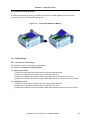
2.6 Connection of QB-780822 to Target System
If connecting the emulation probe (QB-144-EP-01S), connect it to the QB-780822 and the target system by the following procedure.
2.6.1 Connection without using extension probe (QB-144-EP-01S)
QB-780822 for µPD78(F)0822/1 can be connected to the target system without using the extension
probe.
When connecting QB-780822 for µPD78(F)0822/1 and the target system, adjust the height of QB780822 for µPD78(F)0822/1 using the rear spacer so that no stress is applied to the exchange adapter
and target connector.
In addition, take care to maintain insulation with the target system.
Figure 2-13:
Connection without using Extension Probe
QB-780822
Height adjastable
Exchange adapter
Rear spacer
Target connector
40
Preliminary User’s Manual U17172EE1V2UM00
Chapter 2
Setup Procedure
2.6.2 Connection using extension probe (QB-144-EP-01S)
When using the extension probe (QB-144-EP-01S), connect QB-780822 for µPD78(F)0822/1 and the
target system using the following procedure.
(1)
Connecting probe holder
Use the probe holder (included with QB-780822 for µPD78(F)0822/1) for connecting the extension
probe to QB-780822 for µPD78(F)0822/1. How to connect is shown below.
Figure 2-14:
How to use Probe Holder
<1> Connect QB-780822
and the probe
Extension probe
Probe holder
QB-780822
<2> Insert the probe holder in
QB-780822
Insert
Insert the probe holder until it clicks
(Take care with the direction)
Preliminary User’s Manual U17172EE1V2UM00
41
Chapter 2
(2)
Setup Procedure
Connecting extension probe GND lines
The extension probe has three GND lines. Connect these lines to QB-780822 for µPD78(F)0822/1
and the target system using the following procedure.
<1> Fix a GND line of the extension probe to the nut on the bottom surface of QB-780822 for
µPD78(F)0822/1 using a #0 or #1 precision cross-headed screwdriver. (Connection of A and B in
Figure 2-15)
<2> Insert the connector on the top surface of the extension probe in the connector at the bottom
opening of QB-780822 for µPD78(F)0822/1 from the lower side. Take care with the direction.
(Connection of C and QB-780822 for µPD78(F)0822/1 in Figure 2-15)
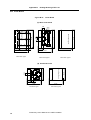
Figure 2-15:
Connection of GND Lines
Target system
<3> Connect the exchange adapter and extension probe to the target connector.
<4> Connect two GND lines of the extension probe on the target system side to the GND block of the
target system. If the pin or screw is fixed on the GND block of the target system, remove the transparent pin cover at the top of the GND line and fix the Y-branch pin of the GND line to the target
system (G in Figure 2-15). In the same manner, if the GND pad on the target system is exposed,
fix the Y-branch pin to the pad on the target system by soldering (H in Figure 2-15). (Recommended iron temperature: 300°C)
<5> If there is only one GND connector on the target system, connect one side and cut off the other
GND lines using nippers, or leave it as is without removing the pin cover.
42
Preliminary User’s Manual U17172EE1V2UM00
Chapter 2
Setup Procedure
<6> The length of the GND line shank (insulation block) is approximately 60 mm. Therefore, as shown
in Figure 2-16, at least one connectable GND is necessary within a radius of approximately
60 mm from the three locations on the extension probe at which the target system is connected.
The GND lines on the emulation probe are soldered at the position of J and K in Figure 2-16.
When soldering the GND line at the position of L, remove a GND line soldered at J or K and solder it at L.
Figure 2-16:
Location at which GND Line can be connected
Target system
Preliminary User’s Manual U17172EE1V2UM00
43
Chapter 2
Setup Procedure
2.6.3 Ensuring isolation
When connecting the target system to the QB-780822 using an emulation probe, perform height regulation using the front spacer or rear spacer of the QB-780822 and ensure isolation from the target system.
Figure 2-17:
Connection Using Emulation Probe
QB-780822
Emulation probe
Exchange adapter
Rear spacer
(can regulate height)
YQ connector
Front spacer
(can regulate height)
Target connector
2.6.4 Precautions related to emulation probe
The following precautions pertain to using the emulation probe.
<1> Be careful that stress of the emulation probe is not placed on the target connector. Moreover,
when removing the emulation probe, remove it slowly while pressing down on the exchange
adapter with a finger so that there is no stress on the target connector.
<2> Be sure to connect the GND wire of the emulation probe to the QB-780822 and the target system.
If it cannot be connected, the impedance of the cable is unstable and could bring about lowering
of signal transmission characteristics or distortion of the output waveform for an input waveform.
44
Preliminary User’s Manual U17172EE1V2UM00
Chapter 2
Setup Procedure
2.7 Power Supply and GND Pin Connection Precautions
For power supplies and GND pins of the target device, be sure to connect all pins to each power supply
or GND.
2.8 Connection of USB Interface Cable and AC Adapter
Plug the USB interface cable supplied with the QB-780822 into the USB connector of the host machine
and also plug it into the USB connector on the rear of the QB-780822.
Plug the AC adapter supplied with the QB-780822 into a receptacle and plug it into the power supply
connector on the rear of the QB-780822.
For QB-780822 connector positions, see Figure 2-18. There are three types of AC adapter plug. Use
the one that has a suitable shape.
Figure 2-18:
Connector Positions
Power supply connector
(Connect AC adapter)
USB connector
(Connect USB interface cable)
2.9 Switching Power On and Off
Be sure to switch the power on and off according to the following procedures.
•
Switching power on
<1> QB-780822 power on
<2> Target system power onNote
<3> Debugger startup
•
Switching power off
<1> Debugger termination
<2> Target system power offNote
<3> QB-780822 power off
Note: In the procedures, <2> is unnecessary if the target system is not connected.
Caution:
If there is a mistake in the order, the target system or QB-780822 may fail.
Preliminary User’s Manual U17172EE1V2UM00
45
[MEMO]
46
Preliminary User’s Manual U17172EE1V2UM00
Chapter 3 Settings at Product Shipment
Table 3-1:
Item
Settings at Shipment
Setting
Remarks
CN5
Main Clock Type III is mounted
CN6
Sub Clock Type II is mounted
Power switch
Set to OFF at shipment.
ON
OFF
Preliminary User’s Manual U17172EE1V2UM00
47
[MEMO]
48
Preliminary User’s Manual U17172EE1V2UM00
Chapter 4 Differences Between Target Interface Circuit and Target Device
This chapter explains the differences between the signal lines of a target interface circuit of the
QB-780822 and the signal lines of a target device
Although the target device is a CMOS circuit, the target interface circuit of the QB-780822 consists of
an emulation circuit that depends on the emulation CPU, TTL, CMOS-IC, or other.
When the target system is debugged by connecting it to the QB-780822, the QB-780822 emulates just
as if the actual target device were operating on the target system.
However, small differences arise because the QB-780822 actually is emulating.
(1) Signals input and output by emulation CPU (µPD78F0822A)
(2)
Signals input and output by emulation CPU (FPGA)
(3) Other signals
The circuits of the QB-780822 for the signals in (1) to (3) above are shown below by target device.
Preliminary User’s Manual U17172EE1V2UM00
49
Chapter 4
Differences Between Target Interface Circuit and Target Device
4.1 For µPD780822 Subseries Emulation
For the signals in (1) to (3) below, see Figure 4-1 Emulation Circuit Equivalent Circuit 1.
(1)
Signals input and output by emulation CPU (µPD78F0822A)
• P03 to P00
• P17 to P10
- load of FET switch in parallel
• P27 to P20
• P33 to P30
• P77 to P70
• P87 to P80
• P97 to P90
- load of two emulation CPU in parallel (only P90)
• P105 to P100 - load of two emulation CPU in parallel
• P113 to P110 - load of two emulation CPU in parallel
• P147 to P140
• P157 to P150
• P120
• P130
• VDD0,VDD1,VDD2
• SMVDD0,SMVDD1
• COM0,COM1,COM2,COM3,VLCD
• AVREF, AVDD
(2)
Signals input and output by emulation CPU (FPGA)
• X1, XT1,RESET, IC/VPPNote
Note: For the µPD78(F)0822/1, the pin name is FLMD0.
(3)
Other signals
• X2, XT2, VSS0, VSS1, VSS2, AVSS, SMVSS0Note, SMVSS1
Note: The pin SMVSS0 is not connected to Ground. It is used for target board detection.
50
Preliminary User’s Manual U17172EE1V2UM00
Chapter 4
Differences Between Target Interface Circuit and Target Device
Figure 4-1:
Emulation Circuit Equivalent Circuit 1 (1/2)
• Probe side
(target system)
• QB-780822 side
P03 to P00,
P17 to P10,
P27 to P20,
P33 to P30,
P120, P130
P90,
P105 to P100,
P113 to P110
VDD
R=0Ω
AVREF, AVDD
µPD78F0822A
Emulation CPU
0.1 µF
PI5A4624TX
VDD
VDD0, VDD1, VDD2
0.1 µF
ST890CD
VDD
SMVDD0, SMVDD1
0.1 µF
ST890CD
µPD78F0822A
Emulation CPU
P147 to P140,
P157 to P150
P87 to P80,
P97 to P91,
COM0, 1, 2, 3, VLCD
Preliminary User’s Manual U17172EE1V2UM00
51
Chapter 4
Differences Between Target Interface Circuit and Target Device
Figure 4-1:
Emulation Circuit Equivalent Circuit 1 (2/2)
• QB-780822 side
• Probe side
(target system)
Level shifter
µPD7885
X1
100 kΩ
X2
33 Ω
OPEN
Level shifter
µPD7885
RESET
100 kΩ
3.3 V
10 kΩ
SMVSS0
Level shifter
µPD7885
Note
AVSS, SMVSS0
VDD0,1,2
IC/VPP
Level shifter
µPD7885
XT1
Level shifter
µPD7885
100 kΩ
XT2
33 Ω
open
Note: SMVSS0 is not connected to common GND.
52
Preliminary User’s Manual U17172EE1V2UM00
FPGA
Emulation CPU
Chapter 5 Cautions
Observe the following cautions.
•
Do not turn off the target power supply during a break (power supply can be turned off only during
RUN).
•
Even when using the product without connecting a target system, connect and use the emulation
probe and exchange adapter.
If the product is used without connecting the emulation probe and exchange adapter, a warning window
is displayed but use is possible.
Preliminary User’s Manual U17172EE1V2UM00
53
[MEMO]
54
Preliminary User’s Manual U17172EE1V2UM00
Appendix A
Notes On Target System Design
This section shows areas on the target system where component mounting is prohibited and areas
where there are component mounting height restrictions.
A.1 When Extension Probe Is Not Used
(1)
For 100-pin GC package
Figure A-1:
For 100-pin GC package
Center of target connector
(common to left/right)
: Exchange adapter area; parts of up to 4.2 mm in height can be mounted
Note
: QB-780822-EE unit area; parts of up to 1 mm in height can be mountedNote
: QB-780822-EE spacer area; mounting parts prohibited
Note: Height can be regulated by using spacer adapters (each adds 2.4 mm on TET-line)
Height can be regulated by using spacer adapters (each adds 5.6 mm on NAIS-line)
Preliminary User’s Manual U17172EE1V2UM00
55
Appendix A
(2)
Notes On Target System Design
For 100-pin GF package
Figure A-2:
For 100-pin GF package
Center of target connector
(common to left/right)
Note
: Exchange adapter area; parts of up to 4.2 mm in height can be mounted
: QB-780822-EE unit area; parts of up to 1 mm in height can be mountedNote
: QB-780822-EE spacer area; mounting parts prohibited
Note: Height can be regulated by using spacer adapters (each adds 2.4 mm on TET-line)
Height can be regulated by using spacer adapters (each adds 5.6 mm on NAIS-line)
56
Preliminary User’s Manual U17172EE1V2UM00
Appendix A
Notes On Target System Design
A.2 When Extension Probe Is Used
(1)
For 100-pin GC package
Figure A-3:
For 100-pin GC package
19.0
19.0
Center of target connector
15.5
15.5
Note
: Exchange adapter area; parts of up to 4.2 mm in height can be mounted
Note
: Extension probe connector area; parts of up to 13.2 mm in height can be mounted
Note: Height can be regulated by using spacer adapters (each adds 2.4 mm on TET-line)
Height can be regulated by using spacer adapters (each adds 5.6 mm on NAIS-line)
Preliminary User’s Manual U17172EE1V2UM00
57
Appendix A
(2)
Notes On Target System Design
For 100-pin GF package
Figure A-4:
For 100-pin GF package
19.0
19.0
Center of target connector
15.5
15.5
: Exchange adapter area; parts of up to 4.2 mm in height can be mountedNote
: Extension probe connector area; parts of up to 13.2 mm in height can be mountedNote
Note: Height can be regulated by using spacer adapters (each adds 2.4 mm on TET-line)
Height can be regulated by using spacer adapters (each adds 5.6 mm on NAIS-line)
58
Preliminary User’s Manual U17172EE1V2UM00
Appendix B
Package Drawings TET Line
B.1 Target Connectors
Figure B-1:
Target Connector for 100-pin QFP GC-package
(a) Package drawing
Top View
Bottom View
–
R
9.0
3
C 1.5
17.0
2.
2
21.0
0.5 X 24 = 12.0
0.5
5.8
0.3
14.0
0.2
Slit width
15.0
16.0
5.8
13.0
20.2
16.6
Slit width
3 – φ 1.0
+ 0.1
2.5
14.0 – 0
4 – φ 2.0 Projection height 1.8
2.5
0.18
0.5
15.0
0.5
5.5
0.2
1.85
1.85
9.45
3.7
1.2
5.1
3.9
Side View
(b) Foot pattern
Preliminary User’s Manual U17172EE1V2UM00
59
Appendix B
Figure B-2:
Package Drawings TET Line
Target Connector for 100-pin QFP GF-package
(a) Package drawing
17.15
21.75
0.5
0.65x19=12.35
0.65
6
0.4
10
3-R1.5
0.5
C1.5
15.25
12
100RB
14.25
4-ø2.0 (A projection height : 1.8 mm)
6.95
0.23
1.2
3.7
1.85
9.45
3.9
17.4
0.25
15.25
0.5
(21.75)
(b) Foot pattern
60
Preliminary User’s Manual U17172EE1V2UM00
23.65
21.75
3-Ø1.0
28.25
0.65x29=18.85
7
20.75
23.9
TET
Appendix B
Package Drawings TET Line
B.2 Exchange Adapters
Exchange Adapter for 100-pin QFP GC-package
22.4
21.55
0.5 × 24 = 12.0
4 – φ 1.0
15.0
33.0
0.5
4 – φ 2.3
16.6
C 2.0
Figure B-3:
10.9
13.3
15.7
18.1
Exchange Adapter for 100-pin QFP GF-package
30.0
21.55
0.5 × 24 = 12.0
15.0
4 – φ 1.0
33.0
0.5
4 – φ 2.3
16.6
C 2.0
Figure B-4:
10.9
13.3
15.7
18.1
Preliminary User’s Manual U17172EE1V2UM00
61
Appendix B
Package Drawings TET Line
B.3 YQ Connectors
Figure B-5:
YQ Connector for 100-pin QFP GC-package
Top View
Bottom View
16.6
4
0.5 X 24 = 12.0
5.8
–
0.5
0.2
.2
φ2
14.1
17.3
16.1
15.3
23.0
5.8
13.4
21.0
C 1.5
2
3 – φ 1.0
13.4
R
3.
R
–
–
4
4
10.9
13.3
15.7
2
2.
18.1
Side View
2.3 1.2
3.9
2.2
0.25
62
3.1
7.4
2.5
0.25 X 0.3
9.0
3.1
3.7
0.3
0.4
Preliminary User’s Manual U17172EE1V2UM00
Appendix B
Figure B-6:
Package Drawings TET Line
YQ Connector for 100-pin QFP GF-package
23.75
17.4
0.65x19=12.35
0.65
14.15
6
C1.5
3-R2.5
0.4
C2.0
21.25
20.2
24.05
21.65
19.25
16.85
7
3-Ø1.0
0.65
23.9
0.65x29=18.85
100RB
10.35
4-Ø2.2
14.75
12.75
0.4
15.15
17.55
7.4
2.3
2.2
0.25
3.1
1.2
0.25
2.5
3.7
0.3
9.9
30.25
TET
0.4
Preliminary User’s Manual U17172EE1V2UM00
63
Appendix B
Package Drawings TET Line
B.4 Mount Adapters
Figure B-7:
Mount Adapter for 100-pin QFP GC-package
Top View
Bottom View
16.6
3.
2
3 – φ 1.0
R
R
2
2.
13.4
2.3
3.9
2.15 1.6
64
3.1
7.4
1.2
Side View
0.23
0.58
Preliminary User’s Manual U17172EE1V2UM00
17.3
C 1.5
14.1
5.8
13.4
21.0
23.0
.2
φ2
–
0.2
17.1
15.12
4
0.5
0.5 X 24 = 12.0
5.8
Appendix B
Figure B-8:
Package Drawings TET Line
Mount Adapter for 100-pin QFP GF-package
23.75
0.65x19=12.35
0.65
14.1
6
3-R2.5
C1.5
100RB
20.2
7
23.9
TET
3-Ø1.0
4-Ø2.2
17.4
7.4
2.3
0.25
16.57
(23.07)
3.1
1.2
* Applicable size of IC package : IC body size 14.0 x 20.0 mm
IC outer size 17.6 x 23.6 mm
2.25
30.25
0.65x29=18.85
0.65
C2.0
0.5
Preliminary User’s Manual U17172EE1V2UM00
65
Appendix B
Package Drawings TET Line
2.5 Check Pin Adapter
Figure B-9:
Check Pin Adapter 144-pin QFP
49
2
1
2
1
CN6
50
CN5
CN4
15
20
50
49
50
2
16
25
39
CP5
49
10.75
1
10.75
15
8.5
30
15
CP1
1
40
2
CP6
20
90
CP2
20
CP3
CP7
CP8
15
CP4
40
40
80
66
Preliminary User’s Manual U17172EE1V2UM00
Appendix B
Package Drawings TET Line
2.6 Spacer Adapters
Figure B-10:
Spacer Adapter for 100-pin QFP GC-package
C 2.0
Top View
4 – φ 1.0
21.55
15.0
0.5 × 24 = 12.0
0.5
4 – φ 2.3
16.6
10.9
13.3
15.7
18.1
φ 0.3
φ 1.03
Preliminary User’s Manual U17172EE1V2UM00
0.8
2.4
2.7
φ 3.30
5.9
Side View
67
Appendix B
Figure B-11:
Package Drawings TET Line
Spacer Adapter for 100-pin QFP GF-package
23.75
17.4
14.47
5.9
0.65x19=12.35
2.7 2.4
4-Ø2.2
10.35
4-Ø1.0
12.75
15.15
17.55
68
Preliminary User’s Manual U17172EE1V2UM00
1.03
4.5
3.55
30.25
23.9
20.97
0.7
0.65x29=18.85
16.85
19.25
21.65
24.05
0.65
0.3
C2.0
0.65
Appendix B
Package Drawings TET Line
B.7 Emulation Probe
Figure B-12:
Emulation Probe 144-pin
Frame ground x 8
Frame ground x 8
Preliminary User’s Manual U17172EE1V2UM00
69
Appendix B
Package Drawings TET Line
B.8 Clock Board
Figure B-13:
Clock Board
(a) Main clock board
2.54
1
1
1
21.78
5.08
21.78
7.62
7.62
Main Clock Type III
Main Clock Type II
C2’
8
8
3.27
C2
S1
2.0
5.81
15.43
15.43
15.43
Main Clock Type I
Main Clock Type II
Main Clock Type II
(b) Sub Clock board
5
C2’
5
2.54
15.43
15.43
Sub Clock Type I
Sub Clock Type II
Preliminary User’s Manual U17172EE1V2UM00
14.16
14.16
C2
I
70
Sub Clock Type II
2.54
1
C1
OSC1
Clock Type
OSC1’
C1’
Sub
1
4.54
21.78
C1
OSC1
OSC1’
S2
S6
8
7.62
C1’
S3
S5
Main Clock Type I
S4
5.81
φ 0.9
Appendix C
Package Drawings NAIS Line
C.1 Target Connectors
Figure C-1:
Target Connector for 100-pin QFP GC-package
(a) Package drawing
050
(b) Foot pattern
Preliminary User’s Manual U17172EE1V2UM00
71
Appendix C
Figure C-2:
Package Drawings NAIS Line
Target Connector for 100-pin QFP GF-package
(a) Package drawing
(b) Foot pattern
72
Preliminary User’s Manual U17172EE1V2UM00
Appendix C
Package Drawings NAIS Line
C.2 Exchange Adapters
Figure C-3:
Exchange Adapter for 100-pin QFP GC-package
Figure C-4:
Exchange Adapter for 100-pin QFP GF-package
Preliminary User’s Manual U17172EE1V2UM00
73
Appendix C
Package Drawings NAIS Line
C.3 Mount Adapters
74
Figure C-5:
Mount Adapter for 100-pin QFP GC-package
Figure C-6:
Mount Adapter for 100-pin QFP GF-package
Preliminary User’s Manual U17172EE1V2UM00
Appendix C
Package Drawings NAIS Line
C.4 Check Pin Adapter
Figure C-7:
Check Pin Adapter 100-pin QFP
Preliminary User’s Manual U17172EE1V2UM00
75
Appendix C
Package Drawings NAIS Line
C.5 Spacer Adapters
76
Figure C-8:
Spacer Adapter for 100-pin QFP GC-package
Figure C-9:
Spacer Adapter for 100-pin QFP GF-package
Preliminary User’s Manual U17172EE1V2UM00
Appendix C
Package Drawings NAIS Line
C.6 Emulation Probe
Figure C-10:
Emulation Probe 144-pin
Frame ground x 8
Frame ground x 8
Preliminary User’s Manual U17172EE1V2UM00
77
Appendix C
Package Drawings NAIS Line
C.7 Clock Board
Figure C-11:
Clock Board
(a) Main clock board
2.54
1
1
1
21.78
5.08
21.78
7.62
7.62
Main Clock Type III
Main Clock Type II
C2’
8
8
3.27
C2
S1
2.0
5.81
15.43
15.43
15.43
Main Clock Type I
Main Clock Type II
Main Clock Type II
(b) Sub Clock board
5
C2’
5
2.54
15.43
15.43
Sub Clock Type I
Sub Clock Type II
Preliminary User’s Manual U17172EE1V2UM00
14.16
14.16
C2
I
78
Sub Clock Type II
2.54
1
C1
OSC1
Clock Type
OSC1’
C1’
Sub
1
4.54
21.78
C1
OSC1
OSC1’
S2
S6
8
7.62
C1’
S3
S5
Main Clock Type I
S4
5.81
φ 0.9
Appendix D
Target Interface Definition
D.1 Target interface definition on TCN1-3Note
The table shows the definition of the TCN1-3 connector on the emulation board and the related pin on
the target device (100-pin QFP).
CN
TCN1.01
TCN1.02
TCN1.03
TCN1.04
TCN1.05
TCN1.06
TCN1.07
TCN1.08
TCN1.09
TCN1.10
TCN1.11
TCN1.12
TCN1.13
TCN1.14
TCN1.15
TCN1.16
TCN1.17
TCN1.18
TCN1.19
TCN1.20
TCN1.21
TCN1.22
TCN1.23
TCN1.24
TCN1.25
TCN1.26
TCN1.27
TCN1.28
TCN1.29
TCN1.30
TCN1.31
TCN1.32
TCN1.33
TCN1.34
TCN1.35
TCN1.36
TCN1.37
TCN1.38
TCN1.39
TCN1.40
TCN1.41
TCN1.42
TCN1.43
TCN1.44
TCN1.45
TCN1.46
TCN1.47
TCN1.48
TCN1.49
TCN1.50
Note: TCN1 50pins
TCN2 50pins
TCN3 50pins
Device
31
42
32
33
36
34
35
37
38
39
40
41
49
50
51
52
53
54
56
43
58
44
57
45
46
-
Axk5s50330p
Axk6s50635
Axk5s50330p
47
55
48
CN
TCN3.01
TCN3.02
TCN3.03
TCN3.04
TCN3.05
TCN3.06
TCN3.07
TCN3.08
TCN3.09
TCN3.10
TCN3.11
TCN3.12
TCN3.13
TCN3.14
TCN3.15
TCN3.16
TCN3.17
TCN3.18
TCN3.19
TCN3.20
TCN3.21
TCN3.22
TCN3.23
TCN3.24
TCN3.25
TCN3.26
TCN3.27
TCN3.28
TCN3.29
TCN3.30
TCN3.31
TCN3.32
TCN3.33
TCN3.34
TCN3.35
TCN3.36
TCN3.37
TCN3.38
TCN3.39
TCN3.40
TCN3.41
TCN3.42
TCN3.43
TCN3.44
TCN3.45
TCN3.46
TCN3.47
TCN3.48
TCN3.49
TCN3.50
Device
12
22
13
21
11
23
10
24
9
25
8
26
7
27
6
28
14
29
15
30
16
17
20
18
19
64
68
67
59
60
66
65
61
63
62
CN
TCN2.01
TCN2.02
TCN2.03
TCN2.04
TCN2.05
TCN2.06
TCN2.07
TCN2.08
TCN2.09
TCN2.10
TCN2.11
TCN2.12
TCN2.13
TCN2.14
TCN2.15
TCN2.16
TCN2.17
TCN2.18
TCN2.19
TCN2.20
TCN2.21
TCN2.22
TCN2.23
TCN2.24
TCN2.25
TCN2.26
TCN2.27
TCN2.28
TCN2.29
TCN2.30
TCN2.31
TCN2.32
TCN2.33
TCN2.34
TCN2.35
TCN2.36
TCN2.37
TCN2.38
TCN2.39
TCN2.40
TCN2.41
TCN2.42
TCN2.43
TCN2.44
TCN2.45
TCN2.46
TCN2.47
TCN2.48
TCN2.49
TCN2.50
Device
94
1
93
5
3
4
2
100
99
98
97
96
95
92
91
90
79
89
78
88
77
87
76
86
75
85
73
84
72
83
74
82
71
81
70
80
69
(connector vendor NAIS, counter part usable Axk6s50635)
(connector vendor NAIS, counter part usable Axk5s50330p)
(connector vendor NAIS, counter part usable Axk6s50635)
Preliminary User’s Manual U17172EE1V2UM00
79
Appendix D
Target Interface Definition
The counter parts of the TCN1-3 could be used of same type. For different height or ordering contact
the connector vendor directly.
This is only an information for customer specific adaptation, in case of not using the NEC adapter line.
80
Preliminary User’s Manual U17172EE1V2UM00
Facsimile Message
From:
Name
Company
Tel.
Although NEC has taken all possible steps
to ensure that the documentation supplied
to our customers is complete, bug free
and up-to-date, we readily accept that
errors may occur. Despite all the care and
precautions we've taken, you may
encounter problems in the documentation.
Please complete this form whenever
you'd like to report errors or suggest
improvements to us.
FAX
Address
Thank you for your kind support.
North America
Hong Kong, Philippines, Oceania
NEC Electronics America Inc.
NEC Electronics Hong Kong Ltd.
Corporate Communications Dept. Fax: +852-2886-9022/9044
Fax: 1-800-729-9288
1-408-588-6130
Korea
Europe
NEC Electronics Hong Kong Ltd.
NEC Electronics (Europe) GmbH
Seoul Branch
Market Communication Dept.
Fax: 02-528-4411
Fax: +49(0)-211-6503-1344
Asian Nations except Philippines
NEC Electronics Singapore Pte. Ltd.
Fax: +65-6250-3583
Japan
NEC Semiconductor Technical Hotline
Fax: +81- 44-435-9608
Taiwan
NEC Electronics Taiwan Ltd.
Fax: 02-2719-5951
I would like to report the following error/make the following suggestion:
Document title:
Document number:
Page number:
If possible, please fax the referenced page or drawing.
Document Rating
Excellent
Good
Acceptable
Poor
Clarity
Technical Accuracy
Organization
CS 99.1