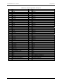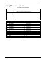
1
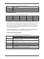
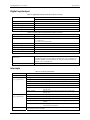
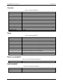
PCI-DAS6402/16 PCI Bus-Compatible Data Acquisition Board User's Guide Document Revision 7, June, 2006 © Copyright 2006, Measurement Computing Corporation Your new Measurement Computing product comes with a fantastic extra — Management committed to your satisfaction! Refer to www.mccdaq.com/execteam.html for the names, titles, and contact information of each key executive at Measurement Computing. Thank you for choosing a Measurement Computing product—and congratulations! You own the finest, and you can now enjoy the protection of the most comprehensive warranties and unmatched phone tech support. It’s the embodiment of our two missions: ! To offer the highest-quality, computer-based data acquisition, control, and GPIB hardware and software available—at the best possible price. ! To offer our customers superior post-sale support—FREE. Whether providing unrivaled telephone technical and sales support on our latest product offerings, or continuing that same first-rate support on older products and operating systems, we’re committed to you! Lifetime warranty: Every hardware product manufactured by Measurement Computing Corporation is warranted against defects in materials or workmanship for the life of the product. Products found defective are repaired or replaced promptly. Lifetime Harsh Environment Warranty®: We will replace any product manufactured by Measurement Computing Corporation that is damaged (even due to misuse) for only 50% of the current list price. I/O boards face some tough operating conditionssome more severe than the boards are designed to withstand. When a board becomes damaged, just return the unit with an order for its replacement at only 50% of the current list price. We don’t need to profit from your misfortune. By the way, we honor this warranty for any manufacturer’s board that we have a replacement for. 30 Day Money Back Guarantee: You may return any Measurement Computing Corporation product within 30 days of purchase for a full refund of the price paid for the product being returned. If you are not satisfied, or chose the wrong product by mistake, you do not have to keep it. Please call for an RMA number first. No credits or returns accepted without a copy of the original invoice. Some software products are subject to a repackaging fee. These warranties are in lieu of all other warranties, expressed or implied, including any implied warranty of merchantability or fitness for a particular application. The remedies provided herein are the buyer’s sole and exclusive remedies. Neither Measurement Computing Corporation, nor its employees shall be liable for any direct or indirect, special, incidental or consequential damage arising from the use of its products, even if Measurement Computing Corporation has been notified in advance of the possibility of such damages. HM PCI-DAS6402_16.doc ii Trademark and Copyright Information TracerDAQ, Universal Library, Harsh Environment Warranty, Measurement Computing Corporation, and the Measurement Computing logo are either trademarks or registered trademarks of Measurement Computing Corporation. Windows, Microsoft, and Visual Studio are either trademarks or registered trademarks of Microsoft Corporation LabVIEW is a trademark of National Instruments. CompactFlash is a registered trademark of SanDisk Corporation. All other trademarks are the property of their respective owners. Information furnished by Measurement Computing Corporation is believed to be accurate and reliable. However, no responsibility is assumed by Measurement Computing Corporation neither for its use; nor for any infringements of patents or other rights of third parties, which may result from its use. No license is granted by implication or otherwise under any patent or copyrights of Measurement Computing Corporation. All rights reserved. No part of this publication may be reproduced, stored in a retrieval system, or transmitted, in any form by any means, electronic, mechanical, by photocopying, recording, or otherwise without the prior written permission of Measurement Computing Corporation. Notice Measurement Computing Corporation does not authorize any Measurement Computing Corporation product for use in life support systems and/or devices without prior written consent from Measurement Computing Corporation. Life support devices/systems are devices or systems which, a) are intended for surgical implantation into the body, or b) support or sustain life and whose failure to perform can be reasonably expected to result in injury. Measurement Computing Corporation products are not designed with the components required, and are not subject to the testing required to ensure a level of reliability suitable for the treatment and diagnosis of people. iii Table of Contents Preface About this User's Guide ......................................................................................................................vi What you will learn from this user's guide ........................................................................................................vi Conventions in this user's guide ........................................................................................................................vi Where to find more information ........................................................................................................................vi Chapter 1 Introducing the PCI-DAS6402/16 ..................................................................................................... 1-1 Overview: PCI-DAS6402/16 features ............................................................................................................ 1-1 Software features ............................................................................................................................................ 1-1 PCI-DAS6402/16 block diagram.................................................................................................................... 1-2 Chapter 2 Installing the PCI-DAS6402/16 ......................................................................................................... 2-1 What comes with your PCI-DAS6402/16 shipment? ..................................................................................... 2-1 Hardware ....................................................................................................................................................................... 2-1 Additional documentation.............................................................................................................................................. 2-1 Optional components ..................................................................................................................................................... 2-1 Unpacking the PCI-DAS6402/16 ................................................................................................................... 2-2 Installing the software .................................................................................................................................... 2-2 Installing the PCI-DAS6402/16...................................................................................................................... 2-2 Configuring the PCI-DAS6402/16 ................................................................................................................. 2-2 Differential input mode.................................................................................................................................................. 2-3 Single-ended input mode ............................................................................................................................................... 2-3 Connecting the board for I/O operations ........................................................................................................ 2-3 Connectors, cables – main I/O connector....................................................................................................................... 2-3 Pinout – main I/O connector .......................................................................................................................................... 2-4 Cabling........................................................................................................................................................................... 2-6 Field wiring, signal termination and conditioning ......................................................................................................... 2-9 Chapter 3 Programming and Developing Applications .................................................................................. 3-1 Programming languages ................................................................................................................................. 3-1 Packaged applications programs..................................................................................................................... 3-1 Register-level programming ........................................................................................................................... 3-1 Chapter 4 Calibrating the PCI-DAS6402/16 ...................................................................................................... 4-1 Overview ........................................................................................................................................................ 4-1 Calibration theory ........................................................................................................................................... 4-1 Chapter 5 Specifications.................................................................................................................................... 5-1 Analog input ................................................................................................................................................... 5-1 Accuracy ........................................................................................................................................................................ 5-2 System throughput ......................................................................................................................................................... 5-3 Crosstalk ........................................................................................................................................................................ 5-3 Analog input drift........................................................................................................................................................... 5-3 Noise performance......................................................................................................................................................... 5-4 Analog output ................................................................................................................................................. 5-4 Accuracy ........................................................................................................................................................................ 5-4 Accuracy components.................................................................................................................................................... 5-5 Analog output pacing and triggering.............................................................................................................................. 5-5 Digital input/output......................................................................................................................................... 5-6 iv PCI-DAS6402/16 User's Guide Interrupts......................................................................................................................................................... 5-6 Counters.......................................................................................................................................................... 5-7 Pacer ............................................................................................................................................................... 5-7 Power consumption ........................................................................................................................................ 5-7 Environmental ................................................................................................................................................ 5-7 Mechanical ..................................................................................................................................................... 5-8 Main connector and pin out ............................................................................................................................ 5-8 Auxiliary DIO connector and pin out ........................................................................................................... 5-11 v Preface About this User's Guide What you will learn from this user's guide This user's guide explains how to install, configure, and use the PCI-DAS6402/16 so that you get the most out of its analog and digital I/O features. This user's guide also refers you to related documents available on our web site, and to technical support resources. Conventions in this user's guide For more information on … Text presented in a box signifies additional information and helpful hints related to the subject matter you are reading. Caution! Shaded caution statements present information to help you avoid injuring yourself and others, damaging your hardware, or losing your data. <#:#> Angle brackets that enclose numbers separated by a colon signify a range of numbers, such as those assigned to registers, bit settings, etc. bold text Bold text is used for the names of objects on the screen, such as buttons, text boxes, and check boxes. For example: 1. Insert the disk or CD and click the OK button. italic text Italic text is used for the names of manuals and help topic titles, and to emphasize a word or phrase. For example: The InstaCal installation procedure is explained in the Quick Start Guide. Never touch the exposed pins or circuit connections on the board. Where to find more information The following electronic documents provide helpful information relevant to the operation of the PCIDAS6402/16. ! ! ! ! ! ! MCC's Specifications: PCI-DAS6402/16 (the PDF version of the Specifications chapter in this guide) is available on our web site at www.mccdaq.com/pdfs/PCI-DAS6402-16.pdf. MCC's Quick Start Guide is available on our web site at www.mccdaq.com/PDFmanuals/DAQ-Software-Quick-Start.pdf. MCC's Guide to Signal Connections is available on our web site at www.mccdaq.com/signals/signals.pdf. MCC's Universal Library User's Guide is available on our web site at www.mccdaq.com/PDFmanuals/sm-ul-user-guide.pdf. MCC's Universal Library Function Reference is available on our web site at www.mccdaq.com/PDFmanuals/sm-ul-functions.pdf. MCC's Universal Library for LabVIEW™ User’s Guide is available on our web site at www.mccdaq.com/PDFmanuals/SM-UL-LabVIEW.pdf. PCI-DAS6402/16 User's Guide (this document) is also available on our web site at www.mccdaq.com/PDFmanuals/PCI-DAS6402-16.pdf. vi Chapter 1 Introducing the PCI-DAS6402/16 Overview: PCI-DAS6402/16 features This manual explains how to install and use the PCI-DAS6402/16. The PCI-DAS6402/16 is a multifunction measurement and control board designed to operate in computers with PCI bus accessory slots. The architecture of the board is loosely based on the original CIO-DAS16, the standard of ISA bus data acquisition. The PCI-DAS6402/16 provides the following features: ! ! ! ! ! ! ! 32 differential or 64 single-ended 16-bit analog inputs 100-pin high density I/O connector and a 40-pin auxiliary connector 200 kHz sample rate Two 16-bit analog outputs with update rates of up to 100 kHz One 16-bit counter 24 DIO bits on the auxiliary connector; four DI bits and 4 DO bits on the 100-pin connector Provides arbitrary waveform generation Analog input ranges are selectable via software as bipolar or unipolar. Bipolar input ranges are ±10 V, ±5 V, ±2.5 V and ±1.25 V. Unipolar input ranges are 0 to 10 V, 0 to 5 V, 0 to 2.5 V and 0 to 1.25 V. The PCIDAS6402/16 has an analog trigger input. The trigger level and direction are software configurable. The PCI-DAS6402/16 board is completely plug and play, with no switches, jumpers or potentiometers to set. All board addresses and interrupt sources are set with software. Software features For information on the features of InstaCal and the other software included with your PCI-DAS6402/16, refer to the Quick Start Guide that shipped with your device. The Quick Start Guide is also available in PDF at www.mccdaq.com/PDFmanuals/DAQ-Software-Quick-Start.pdf. Check www.mccdaq.com/download.htm for the latest software version or versions of the software supported under less commonly used operating systems. 1-1 PCI-DAS6402/16 User's Guide Introducing the PCI-DAS6402/16 PCI-DAS6402/16 block diagram PCI-DAS6402/16 functions are illustrated in the block diagram shown here. Gain and Offset Autocal HOLDING REG Queue Buffer (8K) DAC 0/1 Buffer (16K) ADC Buffer (8K) 32K x 16 SRAM Gain and Offset Autocal DAC0 16 Bit, 100KHz Mux & Gain Analog In 64-ch s.e. 32-ch diff. 16-Bit ADC 16 D 200 kHz Q Memory BUS EOC DAC1 16 Bit, 100KHz 16 TRIG_HI STC ADC Pacer A/D PACER GATE A/D EXTERNAL PACER A/D INTERNAL PACER OUT 40 MHz FIRSTPORTB(7:0) PORTB FIRSTPORTC (7:0) DIN(3:0) DOUT(3:0) Control 24-bits DIO D/A EXTERNAL PACER IN QUEUE CNTL DAC RT CNTL Decoder DMA IRQ CNTL CNTL INTERRUPT IN Local BUS 16 8 Inputs Control/ Status Regs EXTERNAL D/A TRIGGER/PACER GATE DAC Pacer Sample CNTL SSH OUT PORTA DAC CNTL Trigger CNTL A/D START/STOP TRIGGER FIRSTPORTA (7:0) Memory CNTL Boot EEPROM PCI BRIDGE W/BUS MASTER DMA CH0 DMA CH1 Outputs PCI BUS (5V, 32-bit, 33 MHZ) Figure 1-1. PCI-DAS6402/16 functional block diagram 1-2 Control ADC CNTL ANALOG TRIGGER TRIG_LO USER CNTR 0 CTR1 CLK CTR1 OUT Chapter 2 Installing the PCI-DAS6402/16 What comes with your PCI-DAS6402/16 shipment? The following items are shipped with the PCI-DAS6402/16. Hardware ! PCI-DAS6402/16 Additional documentation In addition to this hardware user's guide, you should also receive the Quick Start Guide (available in PDF at www.mccdaq.com/PDFmanuals/DAQ-Software-Quick-Start.pdf). This booklet supplies a brief description of the software you received with your PCI-DAS6402/16 and information regarding installation of that software. Please read this booklet completely before installing any software or hardware. Optional components If you ordered any of the following products with your board, they should be included with your shipment. ! Cables C100FF-x ! BP40-37-x C40FF-x Signal conditioning accessories MCC provides signal termination products for use with the PCI-DAS6402/16. Refer to the "Field wiring, signal termination and conditioning" section on page 2-9 for a complete list of compatible accessory products. 2-1 PCI-DAS6402/16 User's Guide Installing the PCI-DAS6402/16 Unpacking the PCI-DAS6402/16 As with any electronic device, you should take care while handling to avoid damage from static electricity. Before removing the PCI-DAS6402/16 from its packaging, ground yourself using a wrist strap or by simply touching the computer chassis or other grounded object to eliminate any stored static charge. If any components are missing or damaged, notify Measurement Computing Corporation immediately by phone, fax, or e-mail: ! ! ! Phone: 508-946-5100 and follow the instructions for reaching Tech Support. Fax: 508-946-9500 to the attention of Tech Support Email: [email protected] Installing the software Refer to the Quick Start Guide for instructions on installing the software on the Measurement Computing Data Acquisition Software CD. This booklet is available in PDF at www.mccdaq.com/PDFmanuals/DAQ-SoftwareQuick-Start.pdf. Installing the PCI-DAS6402/16 The PCI-DAS6402/16 board is completely plug-and-play. There are no switches or jumpers to set on the board. Configuration is controlled by your system's BIOS. To install your board, follow the steps below. Install the MCC DAQ software before you install your board The driver needed to run your board is installed with the MCC DAQ software. Therefore, you need to install the MCC DAQ software before you install your board. Refer to the Quick Start Guide for instructions on installing the software. 1. Turn your computer off, open it up, and insert your board into an available PCI slot. 2. Close your computer and turn it on. If you are using an operating system with support for plug-and-play (such as Windows 2000 or Windows XP), a dialog box opens as the system loads, indicating that new hardware has been detected. If the information file for this board is not already loaded onto your PC, you are prompted for the disk containing this file. The Measurement Computing Data Acquisition Software CD supplied with your board contains this file. If required, insert the disk or CD and click OK. 3. To test your installation and configure your board, run the InstaCal utility you installed in the previous section. Refer to the Quick Start Guide that came with your board www.mccdaq.com/PDFmanuals/sminstallation.pdf for information on how to initially set up and load InstaCal. If your board has been powered-off for more than 10 minutes, allow your computer to warm up for at least 15 minutes before acquiring data. This warm-up period is required in order for the board to achieve its rated accuracy. The high speed components used on the board generate heat, and it takes this amount of time for a board to reach steady state if it has been powered off for a significant amount of time. Configuring the PCI-DAS6402/16 All of the hardware configuration options on the PCI-DAS6402/16 are software controlled. You can select some of the configuration options using InstaCal, such as the analog input configuration (16 single-ended or eight differential channels), the edge used for triggering when using an external pacer and the source for the two independent counters. Once selected, any program that uses the Universal Library will initialize the hardware according to these selections. 2-2 PCI-DAS6402/16 User's Guide Installing the PCI-DAS6402/16 Information on signal connections General information regarding signal connection and configuration is available in the Guide to Signal Connections. This document is available on our web site at www.mccdaq.com/signals/signals.pdf). Differential input mode When all channels are configured for differential input mode, 32 analog input channels are available. In this mode, the input signal is measured with respect to the low input. The input signal is typically delivered through three wires: ! ! ! The wire carrying the signal to be measured connects to CH# HI. The wire carrying the reference signal connects to CH# LO. The third wire, typically a system ground, is connected to LLGND. Differential input mode is the preferred configuration for applications in noisy environments or when the signal source is referenced to a potential other than PC ground. Single-ended input mode When all channels are configured for single-ended input mode, 64 analog input channels are available. In this mode, the input signal is referenced to the board’s signal ground (LLGND). The input signal is delivered through two wires: ! ! The wire carrying the signal to be measured connects to CH# IN HI. The second wire is connected to LLGND. Connecting the board for I/O operations The PCI-DAS6402/16 uses a 100-pin I/O connector (refer to Table 2-2 on page 2-4 and Table 2-3 on page 2-5). The 100-pin connector provides a much greater signal density than the traditional 37-pin connector. Make accurate notes and pay careful attention to wire connections. In a large system, a misplaced wire can create hours of unnecessary troubleshooting. Connectors, cables – main I/O connector Table 2-1 lists the board connectors, applicable cables, and compatible accessory products for the PCIDAS6402/16. Table 2-1. Board connectors, cables, and compatible hardware Connector type Compatible cable with the main connector Compatible cables with the 40-pin auxiliary connector Compatible accessory products with the C100FF-x Compatible accessory products with the C40FF-x Compatible accessory products with the C40-37F-x cable or with the BP40-37-x and the C37FF-x or C37FFS-x cable ! Main connector: 100-pin high-density Robinson-Nugent ! Auxiliary digital connector: 40-pin header connector C100FF-x ribbon cable. x = length in feet C40FF-x cable (x = length in feet) C40-37F-x cable (x = length in feet) BP40-37 (Translates to a standard CIO-DIO24 type) ! BNC-16SE ! BNC-16DI ! CIO-MINI50 ! CIO-TERM100 ! SCB-50 CIO-MINI40 ! ! ! ! ! ! CIO-MINI37 SCB-37 CIO-ERB24 CIO-ERB08 SSR-RACK24 SSR-RACK08 2-3 PCI-DAS6402/16 User's Guide Installing the PCI-DAS6402/16 Caution! When connecting a cable to the board's I/O connector, make sure that the arrow indicating pin 1 on the board connector lines up with the arrow indicating pin 1 on the cable connector. Incorrectly connected cables can damage the board and the I/O controller. Pinout – main I/O connector Table 2-2. . 32-channel differential mode pin out Signal Name Pin GND EXTERNAL INTERRUPT A/D PACER GATE EXTERNAL D/A TRIGGER/PACER GATE D/A EXTERNAL PACER INPUT A/D INTERNAL PACER OUTPUT DIN3 DIN2 -12 V GND +12 V GND DOUT3 DOUT2 DOUT1 DOUT0 CH31 LO CH31 HI CH30 LO CH30 HI CH29 LO CH29 HI CH28 LO CH28 HI CH27 LO CH27 HI CH26 LO CH26 HI CH25 LO CH25 HI CH24 LO CH24 HI LLGND CH23 LO CH23 HI CH22 LO CH22 HI CH21 LO CH21 HI CH20 LO CH20 HI CH19 LO CH19 HI CH18 LO CH18 HI CH17 LO CH17 HI CH16 LO CH16 HI LLGND 100 99 98 97 96 95 94 93 92 91 90 89 88 87 86 85 84 83 82 81 80 79 78 77 76 75 74 73 72 71 70 69 68 67 66 65 64 63 62 61 60 59 58 57 56 55 54 53 52 51 PCI slot ↓ 2-4 •• •• •• •• •• •• •• •• •• •• •• •• •• •• •• •• •• •• •• •• •• •• •• •• •• •• •• •• •• •• •• •• •• •• •• •• •• •• •• •• •• •• •• •• •• •• •• •• •• •• Pin Signal Name 50 49 48 47 46 45 44 43 42 41 40 39 38 37 36 35 34 33 32 31 30 29 28 27 26 25 24 23 22 21 20 19 18 17 16 15 14 13 12 11 10 9 8 7 6 5 4 3 2 1 GND SSH OUT/DAC PACER OUT PC +5 V A/D STOP TRIGGER IN DIN1 A/D START TRIGGER IN DIN0 ANALOG TRIGGER IN A/D EXTERNAL PACER CTR1 OUT CTR1 GATE CTR1 CLK D/A OUT 1 D/A GND 1 D/A OUT 0 D/A GND 0 CH15 LO CH15 HI CH14 LO CH14 HI CH13 LO CH13 HI CH12 LO CH12 HI CH11 LO CH11 HI CH10 LO CH10 HI CH9 LO CH9 HI CH8 LO CH8 HI LLGND CH7 LO CH7 HI CH6 LO CH6 HI CH5 LO CH5 HI CH4 LO CH4 HI CH3 LO CH3 HI CH2 LO CH2 HI CH1 LO CH1 HI CH0 LO CH0 HI LLGND PCI-DAS6402/16 User's Guide Installing the PCI-DAS6402/16 Table 2-3. 64-channel single-ended mode pin out Signal Name Pin GND EXTERNAL INTERRUPT A/D PACER GATE EXTERNAL D/A TRIGGER/PACER GATE D/A EXTERNAL PACER INPUT A/D INTERNAL PACER OUTPUT DIN3 DIN2 -12 V GND +12 V GND DOUT3 DOUT2 DOUT1 DOUT0 CH63 IN CH31 IN CH62 IN CH30 IN CH61 IN CH29 IN CH60 IN CH28 IN CH59 IN CH27 IN CH58 IN CH26 IN CH57 IN CH25 IN CH56 IN CH24 IN LLGND CH55 IN CH23 IN CH54 IN CH22 IN CH53 IN CH21 IN CH52 IN CH20 IN CH51 IN CH19 IN CH50 IN CH18 IN CH49 IN CH17 IN CH48 IN CH16 IN LLGND 100 99 98 97 96 95 94 93 92 91 90 89 88 87 86 85 84 83 82 81 80 79 78 77 76 75 74 73 72 71 70 69 68 67 66 65 64 63 62 61 60 59 58 57 56 55 54 53 52 51 PCI slot ↓ 2-5 •• •• •• •• •• •• •• •• •• •• •• •• •• •• •• •• •• •• •• •• •• •• •• •• •• •• •• •• •• •• •• •• •• •• •• •• •• •• •• •• •• •• •• •• •• •• •• •• •• •• Pin Signal Name 50 49 48 47 46 45 44 43 42 41 40 39 38 37 36 35 34 33 32 31 30 29 28 27 26 25 24 23 22 21 20 19 18 17 16 15 14 13 12 11 10 9 8 7 6 5 4 3 2 1 GND SSH OUT/DAC PACER OUT PC +5 V A/D STOP TRIGGER IN DIN1 A/D START TRIGGER IN DIN0 ANALOG TRIGGER IN A/D EXTERNAL PACER CTR1 OUT CTR1 GATE CTR1 CLK D/A OUT 1 D/A GND 1 D/A OUT 0 D/A GND 0 CH47 IN CH15 IN CH46 IN CH14 IN CH45 IN CH13 IN CH44 IN CH12 IN CH43 IN CH11 IN CH42 IN CH10 IN CH41 IN CH9 IN CH40 IN CH8 IN LLGND CH39 IN CH7 IN CH38 IN CH6 IN CH37 IN CH5 IN CH36 IN CH4 IN CH35 IN CH3 IN CH34 IN CH2 IN CH33 IN CH1 IN CH32 IN CH0 IN LLGND PCI-DAS6402/16 User's Guide Installing the PCI-DAS6402/16 Table 2-4. Auxiliary/digital connector pin out Signal Name NC NC FIRSTPORTA Bit 0 FIRSTPORTA Bit 1 FIRSTPORTA Bit 2 FIRSTPORTA Bit 3 FIRSTPORTA Bit 4 FIRSTPORTA Bit 5 FIRSTPORTA Bit 6 FIRSTPORTA Bit 7 FIRSTPORTC Bit 0 FIRSTPORTC Bit 1 FIRSTPORTC Bit 2 FIRSTPORTC Bit 3 FIRSTPORTC Bit 4 FIRSTPORTC Bit 5 FIRSTPORTC Bit 6 FIRSTPORTC Bit 7 DGND PC +5V Pin •• •• 40 38 36 34 32 30 28 26 24 22 20 18 16 14 12 10 8 6 4 2 Bottom of board •• •• •• •• •• •• •• •• •• •• •• •• •• •• •• •• •• •• Pin Signal Name 39 37 35 33 31 29 27 25 23 21 19 17 15 13 11 9 7 5 3 1 NC DGND PC +5V DGND NC DGND NC DGND NC DGND FIRSTPORTB Bit 0 FIRSTPORTB Bit 1 FIRSTPORTB Bit 2 FIRSTPORTB Bit 3 FIRSTPORTB Bit 4 FIRSTPORTB Bit 5 FIRSTPORTB Bit 6 FIRSTPORTB Bit 7 NC NC ↓ Cabling Use a C100FF-x 100-pin cable to connect signals to the PCI-DAS6402/16 board. This cable consists of two 50-pin ribbon cables that are joined together at a 100-pin high density header connector (Figure 2-1.) Cable is labeled “Pins 1-50” 49 50 Field Wiring connections: CIO-MINI50 CIO-MINI50/DST CIO-TERM100 CIO-TERM100/DST CIO-SPADE50 SCB-50 Key 50 100 2 1 The red stripe identifies pin # 1 99 100 1 51 Field Wiring connections: CIO-MINI50 CIO-MINI50/DST CIO-TERM100 CIO-TERM100/DST CIO-SPADE50 SCB-50 Key Cable is labeled “Pins 51-100” 51 52 The red stripe identifies pin # 51 Figure 2-1. C100FF-x cable 2-6 PCI-DAS6402/16 User's Guide Installing the PCI-DAS6402/16 For signal connections and termination, you can use the CIO-MINI40 screw terminal board and C40FF-x cable. For connections to 37-pin screw terminal boards, you can use the C40-37F-x cable. 2 The red stripe identifies pin # 1 1 40 2 1 40 39 40-pin Female IDC Connector 39 40-pin Female IDC Connector Figure 2-2. C40FF-x cable 2 The red stripe identifies pin # 1 1 1 20 37 40 19 39 40-pin Female IDC Connector 37-pin Female Dsub Connector Figure 2-3. C40-37F-x cable For digital signal conditioning, you can connect the BP40-37 cable to a C37FF-x or C37FFS-x cable, and then connect one of these cables to the 37-pin connector on MCC’s digital signal conditioning boards. Refer to page 2-9 for a list of compatible accessories. 19 39 40 1 2 37 Key 20 1 The red stripe and arrow identify pin # 1 37-pin Male D Connector with Backplate Assembly 40-pin Female IDC Connector Figure 2-4. BP40-37 cable 2-7 PCI-DAS6402/16 User's Guide Installing the PCI-DAS6402/16 GND FIRSTPORTA BIT 0 FIRSTPORTA BIT 1 FIRSTPORTA BIT 2 FIRSTPORTA BIT 3 FIRSTPORTA BIT 4 FIRSTPORTA BIT 5 FIRSTPORTA BIT 6 FIRSTPORTA BIT 7 FIRSTPORTC BIT 0 FIRSTPORTC BIT 1 FIRSTPORTC BIT 2 FIRSTPORTC BIT 3 FIRSTPORTC BIT 4 FIRSTPORTC BIT 5 FIRSTPORTC BIT 6 FIRSTPORTC BIT 7 GND +5V +5V GND NC GND NC GND NC GND FIRSTPORTB BIT 1 FIRSTPORTB BIT 2 FIRSTPORTB BIT 3 FIRSTPORTB BIT 4 FIRSTPORTB BIT 5 FIRSTPORTB BIT 6 FIRSTPORTB BIT 7 NC Figure 2-5. BP40-37 cable pin out The red stripe identifies pin # 1 1 1 20 20 37 37 19 19 Figure 2-6. C37FF-x cable 1 19 1 20 37 19 Figure 2-7. C37FFS-x cable 2-8 20 37 PCI-DAS6402/16 User's Guide Installing the PCI-DAS6402/16 40-pin to 37-pin signal mapping Signal mapping on the C40-37F-x and the BP40-37-x cables is not 1:1. Table 2-5 lists the pin numbers of the signals on the 40-pin end and the pin numbers of the associated signals on the 37-pin end. Table 2-5. Signal mapping on the C40-37F-x and BP40-37F cables Pin 1 2 3 4 5 6 7 8 9 10 11 12 13 14 15 16 17 18 19 20 21 22 23 24 25 26 27 28 29 30 31 32 33 34 35 36 37 38 39 40 40-pin cable end Signal Name INTERRUPT IN +5V INTERRUPT ENABLE GND Port B 7 Port C 7 Port B 6 Port C 6 Port B 5 Port C 5 Port B 4 Port C 4 Port B 3 Port C 3 Port B 2 Port C 2 Port B 1 Port C 1 Port B 0 Port C 0 GND Port A 7 N/C Port A 6 GND Port A 5 N/C Port A 4 GND Port A 3 N/C Port A 2 GND Port A 1 +5V Port A 0 GND N/C N/C N/C Pin 1 20 2 21 3 22 4 23 5 24 6 25 7 26 8 27 9 28 10 29 11 30 12 31 13 32 14 33 15 34 16 35 17 36 18 37 19 37-pin cable end Signal Name INTERRUPT IN +5V INTERRUPT ENABLE GND Port B 7 Port C 7 Port B 6 Port C 6 Port B 5 Port C 5 Port B 4 Port C 4 Port B 3 Port C 3 Port B 2 Port C 2 Port B 1 Port C 1 Port B 0 Port C 0 GND Port A 7 N/C Port A 6 GND Port A 5 N/C Port A 4 GND Port A 3 N/C Port A 2 GND Port A 1 +5V Port A 0 GND Field wiring, signal termination and conditioning You can use the following MCC screw terminal boards to terminate field signals and route them into the PCIDAS6402/16 board using the C100FF-x cable: ! BNC-16SE – 16-channel single-ended BNC connector box. Details on this product are available on our web ! BNC-16DI – Eight-channel differential BNC connector box. Details on this product are available on our ! CIO-MINI50 – 50-pin screw terminal board. Details on this product are available on our web site at ! CIO-TERM100 – 100 pin, 16 x 4 screw terminal board. Details on this product are available on our web site ! SCB-50 – 50-conductor, shielded signal connection box. Details on this product are available on our web site at www.mccdaq.com/cbicatalog/cbiproduct.asp?dept_id=101&pf_id=713. web site at www.mccdaq.com/cbicatalog/cbiproduct.asp?dept_id=101&pf_id=714. www.mccdaq.com/cbicatalog/cbiproduct.asp?dept_id=102&pf_id=258. at www.mccdaq.com/cbicatalog/cbiproduct.asp?dept_id=102&pf_id=281. site at www.mccdaq.com/cbicatalog/cbiproduct.asp?dept_id=196&pf_id=1168. 2-9 PCI-DAS6402/16 User's Guide Installing the PCI-DAS6402/16 You can use the following MCC screw terminal board to terminate field signals and route them into the PCIDAS6402/16 board using the C40FF-x cable. ! CIO-MINI40 – 50-pin screw terminal board. Details on this product are available on our web site at www.mccdaq.com/cbicatalog/cbiproduct.asp?dept_id=102&pf_id=257. For digital signal conditioning, you can connect the PCI-DAS6402/16 to the following boards using the C4037F-x cable, or the BP40-37 cable with either the C37FF-x or C37FFS-x cable. ! SCB-37 – 37-conductor, shielded signal connection/screw terminal box. Details on this product are ! CIO-MINI37 – 37-pin screw terminal board. Details on this product are available on our web site at ! CIO-ERB24 – 24 Form C relays, 6 Amp relay accessory board for digital signal conditioning. Details on available on our web site at www.mccdaq.com/cbicatalog/cbiproduct.asp?dept_id=196&pf_id=1166. www.mccdaq.com/cbicatalog/cbiproduct.asp?dept_id=102&pf_id=1543. ! ! ! this product are available on our web site at www.mccdaq.com/cbicatalog/cbiproduct.asp?dept_id=123&pf_id=241. CIO-ERB08 – Eight Form C relays, 6 Amp relay accessory board for digital signal conditioning. Details on this product are available on our web site at http://www.mccdaq.com/cbicatalog/cbiproduct.asp?dept_id=123&pf_id=240. SSR-RACK24 – 24-position solid state relay rack. Details on this product are available on our web site at www.mccdaq.com/cbicatalog/cbiproduct.asp?dept_id=122&pf_id=1193. SSR-RACK08 – Eight-channel solid state relay rack. Details on this product are available on our web site at www.mccdaq.com/cbicatalog/cbiproduct.asp?dept_id=122&pf_id=620. 2-10 Chapter 3 Programming and Developing Applications After following the installation instructions in Chapter 2, your board should now be installed and ready for use. Although the board is part of the larger DAS family, in general there may be no correspondence among registers for different boards. Software written at the register level for other DAS models will not function correctly with your board. Programming languages Measurement Computing’s Universal Library™ provides access to board functions from a variety of Windows programming languages. If you are planning to write programs, or would like to run the example programs for Visual Basic or any other language, please refer to the Universal Library User's Guide (available on our web site at www.mccdaq.com/PDFmanuals/sm-ul-user-guide.pdf). Packaged applications programs Many packaged application programs, such as SoftWIREand HP-VEE™, now have drivers for your board. If the package you own does not have drivers for the board, please fax or e-mail the package name and the revision number from the install disks. We will research the package for you and advise how to obtain drivers. Some application drivers are included with the Universal Library package, but not with the application package. If you have purchased an application package directly from the software vendor, you may need to purchase our Universal Library and drivers. Please contact us by phone, fax or e-mail: ! ! ! Phone: 508-946-5100 and follow the instructions for reaching Tech Support. Fax: 508-946-9500 to the attention of Tech Support Email: [email protected] Register-level programming You should use the Universal Library or one of the packaged application programs mentioned above to control your board. Only experienced programmers should try register-level programming. If you need to program at the register level in your application, you can find more information in the Register Map for the PCIDAS6402/16 Series (available at www.mccdaq.com/registermaps/RegMapPCI-DAS6402-16.pdf). 3-1 Chapter 4 Calibrating the PCI-DAS6402/16 Overview The PCI-DAS6402/16 provides self-calibration of the analog inputs and outputs, eliminating the need for external equipment and user adjustments. All adjustments are made via 8-bit calibration DACs and digital potentiometers that are referenced to an on-board factory-calibrated standard. The board is fully calibrated at the factory with calibration coefficients stored in nvRAM. At run time, these calibration factors are loaded into system memory and are automatically retrieved each time a different DAC/ADC range is specified. You can recalibrate any time using factory voltage standards by selecting the Calibrate option in InstaCal. A full calibration typically requires less than two minutes. We strongly recommend that you turn your computer on, and allow at least 60 minutes for the internal computer case temperature to stabilize prior to calibrating the board. Calibration theory Offset calibration for the analog front end is performed via adjustments of the ADC itself. Front-end gain adjustment is performed only via the ADC reference. This strategy was chosen since the gain tolerance of the in-amp circuit is quite good and there is adequate gain tuning range using only the ADC. Analog input calibration is shown in Figure 4-1. Analog In ADC Calibration Reference Offset Adjust Offset Adjust Ref. Unipolar/ Bipolar Digital offset potential Figure 4-1. Analog input calibration 4-1 Digital gain potential PCI-DAS6402/16 User's Guide Calibrating the PCI-DAS6402/16 The analog output circuits are calibrated for gain and offset. Gain calibration of the analog outputs is performed via DAC reference front-end calibration system. Analog output calibration is shown in Figure 4-2. This circuit is duplicated for both DAC0 and DAC1. DAC Analog Out Ref Trim DAC Coarse Trim DAC Fine Gain Adjust Trim DAC Coarse Offset Adjust Trim DAC Fine Figure 4-2. Analog output calibration 4-2 Chapter 5 Specifications Typical for 25 °C unless otherwise specified. Specifications in italic text are guaranteed by design. Analog input Table 1. Analog input specifications A/D converter type Resolution Number of channels Input ranges (SW programmable) Polarity A/D pacing (SW programmable) Burst mode A/D gate sources A/D gating modes A/D trigger sources A/D triggering modes Data transfer Configuration memory Channel/gain queue A/D conversion time Calibration AD976A, successive approximation ADC 16 bits 64 single ended; 32 differential Bipolar: ±10 V, ±5 V, ±2.5 V, ±1.25 V Unipolar: 0 to 10 V, 0 to 5 V, 0 to 2.5 V, 0 to 1.25 V Unipolar/Bipolar, software selectable Internal counter – ASIC External source (A/D external pacer) Software polled Software selectable option, burst rate = 5 µS. Valid for a fixed input range only. External digital (A/D Pacer Gate) External analog (Analog Trigger In) External digital: Programmable, active high or active low, level, or edge External analog: Software-configurable for: ! Above or below reference ! Positive or negative hysteresis ! In or out of window Trigger levels set by D/A OUT 0 and/or D/A OUT 1. External digital (A/D start trigger in and A/D stop trigger in) External analog (analog trigger in) External digital: Software-configurable for rising or falling edge. External analog: Software-configurable for positive or negative slope. Trigger levels set by D/A OUT 0 and/or D/A OUT 1. Pre-/post-trigger: Unlimited number of pre-trigger samples, 16 Meg post-trigger samples. Compatible with both digital and analog trigger options. From 8k RAM buffer via DMA (demand or non-demand mode) using scatter gather. Programmed I/O 8K words Up to 8K elements. Programmable channel, gain, and offset. 5 µS Auto-calibration, calibration factors for each range stored on board in non-volatile RAM. 5-1 PCI-DAS6402/16 User's Guide Specifications Accuracy 200 kHz sampling rate, single channel operation and a 60 minute warm-up. Accuracies are listed for operational temperatures within ±2 ºC of internal calibration temperature. Calibrator test source high side tied to Channel 0 High and low side tied to Channel 0 Low. Low-level ground is tied to Channel 0 Low at the user connector. Table 2. Absolute accuracy Range ±10.000 V ±5.000 V ±2.500 V ±1.250 V 0 V to +10.000 V 0 V to +5.000 V 0 V to +2.500 V 0 V to +1.250 V Absolute accuracy ±3.0 LSB ±3.0 LSB ±4.5 LSB ±4.5 LSB ±3.0 LSB ±3.0 LSB ±4.5 LSB ±4.5 LSB Table 3. Accuracy components Range Gain error Offset error DLE ILE ±10.00 V ±5.000 V ±2.500 V ±1.250 V 0 to +10.00 V 0 to +5.000 V 0 to +2.500 V 0 to +1.250 V ±1.5 max ±1.5 max ±2.0 max ±2.0 max ±1.5 max ±1.5 max ±1.5 max ±1.5 max ±1.5 max ±1.5 max ±2.5 max ±2.5 max ±1.5 max ±1.5 max ±3.0 max ±3.0 max ±1.75 max ±1.75 max ±1.75 max ±1.75 max ±1.75 max ±1.75 max ±1.75 max ±1.75 max ±2 max ±2 max ±2 max ±2 max ±2 max ±2 max ±2 max ±2 max Each PCI-DAS6402/16 is tested at the factory to assure the board’s overall error does not exceed accuracy limits described in Table 2 above. As shown in Table 3, total analog input error is a combination of gain, offset, differential linearity and integral linearity error. The theoretical worst-case error of the board may be calculated by summing these component errors. Worst case errors are realized only in the unlikely event that each of the component errors are at their maximum level, and causing error in the same direction. 5-2 PCI-DAS6402/16 User's Guide Specifications System throughput Table 4. System throughput specifications Condition Calibration coefficients ADC rate (max) 1. Single channel, single input range. 2. Multiple channel, single input range 3. Single channel, multiple input ranges. All samples in unipolar OR bipolar mode. 4. Multiple channels, multiple input ranges. All samples in unipolar OR bipolar mode. 5. Multiple channels, multiple input ranges, switching Unipolar/bipolar mode 6. Multiple channel, single input range, switching Unipolar/bipolar mode. Per specified range Per specified range Default to value for cbAInScan() range 200 kHz 200 kHz 200 kHz Default to value for cbAInScan() range 200 kHz Default to value for cbAInScan() range 200 kHz Default to value for cbAInScan() range 200 kHz Note 1: For conditions 1-2 above, specified accuracy is maintained at rated throughput. Conditions 3-6 apply calibration coefficients which correspond to the range value selected in cbAInScan(). These coefficients remain unchanged throughout the scan. Errors of up to 25 counts may be incurred when switching gains while in bipolar or unipolar mode only (conditions 3 and 4). Errors of up to 100 counts may be incurred when mixing unipolar/bipolar modes (conditions 5 and 6). Crosstalk Crosstalk is defined here as the influence of one channel upon another when scanning two channels at the maximum rate. A full scale 100 Hz triangle wave is input on Channel 1; Channel 0 is tied to Analog Ground at the 100 pin user connector. The table below summarizes the influence of Channel 1 on Channel 0 with the effects of noise removed. The residue on Channel zero is described in LSBs. Table 5. Crosstalk specifications Condition Crosstalk Per channel rate ADC rate Same range to same range Any range to any range 3 LSB pk-pk 6 LSB pk-pk 100 kHz 100 kHz 200 kHz 200 kHz Analog input drift Table 6. Analog input drift specifications Analog input full-scale gain drift Analog input zero drift Overall analog input drift Common mode range CMRR @ 60 Hz Input impedance Absolute maximum input voltage 0.25 LSB/°C max 0.21 LSB/°C max 0.46 LSB/°C max ±10 V -80 dB min 10 MegOhm min ! Channel 0: ±15 V, power on or off ! Channels 1-63: –40 V to +55 V, power on or off 60 minutes Warm-up time 5-3 PCI-DAS6402/16 User's Guide Specifications Noise performance Table 7 below summarizes the noise performance for the PCI-DAS6402/16. Noise distribution is determined by gathering 50K samples with inputs tied to ground at the user connector. Table 7. Board noise performance Range Standard Deviation % within ±2 counts % within ±1 count MaxCounts LSBrms* ±10.00 V ±5.000 V ±2.500 V ±1.250 V 0 to +10.00 V 0 to +5.000 V 0 to +2.500 V 0 to +1.250 V 0.8 0.8 0.8 0.9 0.9 0.9 0.9 1.0 98% 98% 98% 97% 97% 97% 97% 95% 78% 78% 78% 73% 73% 73% 73% 68% 9 9 9 10 10 10 10 11 1.4 1.4 1.4 1.5 1.5 1.5 1.5 1.7 * RMS noise is defined as the peak-to-peak bin spread divided by 6.6 Analog output Table 8. Analog output specifications A/D converter type Resolution Number of Channels Voltage ranges Monotonicity Analog output full-scale gain drift Analog output zero drift Overall analog output drift Slew rate Settling time Current drive Output short-circuit duration Output coupling Output impedance Power up and reset AD669BR 16-bits 2 ±10 V, ±5 V, 0 to 10 V, 0 to 5 V. Each channel independently programmable. Guaranteed monotonic over temperature ±0.55 LSB/°C 10 V ranges: ±0.25 LSB/°C; 5 V ranges: ±0.45 LSB/°C 10 V ranges: ±0.8 LSB/°C; 5 V ranges: ±1.0 LSB/°C 10 V Ranges: 5 V/µs; 5 V ranges: 2.5 V/µs; 20 V step to .0008%:13 µs max; 10 V step to .0008%:6 µs typ ±15 mA Indefinite @ 25 mA DC 0.1 ohms DACs cleared to 0 volts ±75 mV max Accuracy Table 9. Absolute accuracy specifications Range Absolute accuracy ±10.000 V ±5.000 V 0 to +10.000 V 0 to +5.000 V ±4.0 LSB ±4.0 LSB ±4.0 LSB ±4.0 LSB 5-4 PCI-DAS6402/16 User's Guide Specifications Table 10. Typical accuracy specifications Range Typical accuracy ±10.000 V ±5.000 V 0 to +10.00 V 0 to +5.000 V ±3.5 LSB ±3.5 LSB ±3.5 LSB ±3.5 LSB Accuracy components Table 11. Accuracy component specifications Range Gain error (LSB) Offset error (LSB) DLE (LSB) ILE (LSB) ±10.000 V ±5.000 V 0 to +10.00 V 0 to +5.000 V ±2.0 max, ±1.5 typ ±2.0 max, ±1.5 typ ±2.0 max, ±1.5 typ ±2.0 max, ±1.5 typ ±2.0 max, ±1.0 typ ±2.0 max, ±1.0 typ ±2.0 max, ±1.0 typ ±2.0 max, ±1.0 typ ±1.0 max, ±0.5 typ ±1.0 max, ±0.5 typ ±1.0 max, ±0.5 typ ±1.0 max, ±0.5 typ ±1.0 max, ±0.5 typ ±1.0 max, ±0.5 typ ±1.0 max, ±0.5 typ ±1.0 max, ±0.5 typ Each PCI-DAS6402/16 is tested at the factory to assure the board’s overall error does not exceed ±4.0 LSB. Total analog output error is a combination of gain, offset, integral linearity, and differential linearity error. The theoretical worst-case error of the board may be calculated by summing these component errors. Worst case error is realized only in the unlikely event that each of the component errors are at their maximum level, and causing error in the same direction. Although an examination of the chart and a summation of the maximum theoretical errors shows that the board could theoretically exhibit a ±6.0 LSB error, our testing assures this error is never realized in a board that we ship. Typical accuracy is derived directly from the various component typical errors. This typical, maximum error calculation for the PCI-DAS6402/16 yields ±3.5 LSB. However, this again assumes that each of the errors contributes in the same direction and the ±3.5 LSB specification is quite conservative. Analog output pacing and triggering Table 12. Analog output pacing and triggering specifications D/A pacing (SW programmable) D/A gate sources (SW programmable) D/A gating modes D/A trigger sources D/A triggering modes Data transfer Throughput Internal counter – ASIC External source (D/A external pacer) Software paced ! External digital (external D/A trigger/pacer gate) ! External analog (analog trigger in) ! External digital: Programmable, active high or active low, level or edge ! External analog: Software-configurable for above or below reference. Gating levels set by DAC0 or DAC1 External digital (external D/A trigger/pacer gate) Software triggered External digital: Software-configurable for rising or falling edge. ! From 16k RAM buffer via DMA (demand or non-demand mode) using scatter gather. ! Programmed I/O ! Update DACs individually or simultaneously (SW selectable) 100 kHz max per channel, 2 channels simultaneous 5-5 PCI-DAS6402/16 User's Guide Specifications Digital input/output Table 13. Digital input/output specifications (main connector) Digital type (main connector) Configuration Output high voltage (IOH = -0.4 mA) Output low voltage (IOL = 8 mA) Input high voltage Input low voltage Output: 74LS175 Input: 74LS244 4 inputs, 4 outputs (DIN0 through DIN3; DOUT0 to DOUT3) 2.7 V min 0.5 V max 2.0 V min, 7 volts absolute max 0.8 V max, –0.5 volts absolute min Table 14. Digital input/output specifications (DIO connector) Digital type (digital I/O connector) Number of I/O Configuration Input high voltage Input low voltage Output high voltage (IOH = -2.5 mA) Output low voltage (IOL = 2.5 mA) Power-up / reset state 82C55 24 (FIRSTPORTA Bit 0 through FIRSTPORTC Bit 7) ! 2 banks of 8 and 2 banks of 4 or ! 3 banks of 8 or ! 2 banks of 8 with handshake 2.0 V min, 5.5 V absolute max 0.8 V max, –0.5 V absolute min 3.0 V min 0.4 V max Input mode (high impedance) Table 15. Simultaneous sample and hold specifications SSH output SSH polarity TTL-compatible output, HOLD is asserted from start of the conversion for Channel 0 through conversion of the last channel in the scan. Available at user connector (SSH OUT / D/A PACER OUT). This pin is software selectable as SSH OUT or D/A PACER OUT. HOLD high (default) or HOLD low, software selectable Interrupts Table 16. Interrupt specifications Interrupts Interrupt enable ADC interrupt sources (sw programmable) DAC interrupt sources (sw programmable) External interrupt PCI INTA# - mapped to IRQn via PCI BIOS at boot-time Programmable through PLX9080 DAQ_ACTIVE: Interrupt is generated when a DAQ sequence is active. DAQ_STOP: Interrupt is generated when A/D Stop Trigger In is detected. DAQ_DONE: Interrupt is generated when a DAQ sequence completes. DAQ_FIFO_1/4_FULL: Interrupt is generated when ADC FIFO is ¼ full. DAQ_SINGLE: Interrupt is generated after each conversion completes. DAQ_EOSCAN: Interrupt is generated after the last channel is converted in multichannel scans. DAQ_EOSEQ: Interrupt is generated after each interval delay during multichannel scans. DAC_ACTIVE: Interrupt is generated when DAC waveform circuitry is active. DAC_DONE: Interrupt is generated when a DAC sequence completes. DAC_FIFO_1/4_EMPTY: Interrupt is generated DAC FIFO is ¼ empty. DAC_HIGH_CHANNEL: Interrupt is generated when the DAC high channel output is updated. DAC_RETRANSMIT: Interrupt is generated when the end of a waveform sequence has occurred in retransmit mode. Interrupt is generated via edge-sensitive transition on the External Interrupt pin. Rising/falling edge polarity software selectable. 5-6 PCI-DAS6402/16 User's Guide Specifications Counters Table 17. Counter specifications User counter type Configuration Counter 1 source Counter 1 gate Counter 1 output Clock input frequency High pulse width (clock input) Low pulse width (clock input) Gate width high Gate width low Input low voltage Input high voltage Output low voltage Output high voltage 82C54 One down counter, 16 bits. Counters 2 and 3 not used. External from connector (CTR1 CLK) Available at connector (CTR1 GATE). Available at connector (CTR1 OUT). 10 MHz max 30 nS min 50 nS min 50 nS min 50 nS min 0.8 V max 2.0 V min 0.4 V max 3.0 V min Pacer Table 18. Pacer specifications ADC pacer type Configuration ADC pacer Source ADC pacer Gate ADC pacer Out DAC Pacer type Configuration DAC pacer source DAC pacer gate DAC pacer out Internal pacer crystal oscillator Frequency accuracy ASIC 1 down counter, 24 bits (1 scan interval, 1 sample interval) 40 MHz Internally controlled by software/hardware trigger. ADC pacer clock, available at user connector (A/D pacer out) ASIC 1 down counter, 24 bits (1 scan interval, 1 sample interval) 40 MHz or 100 kHz internal source. Software selectable Internally controlled by software/hardware trigger. DAC pacer clock. Available at connector. (SSH OUT / D/A PACER OUT). This pin is software selectable as SSH OUT or D/A PACER OUT. 40 MHz 50 ppm Power consumption Table 19. Power consumption specifications +5 V 2.9A typical, 3.3 max Environmental Table 20. Environmental specifications Operating temperature range Storage temperature range Humidity 0 to 70 °C -40 to 100 °C 0 to 95% non-condensing 5-7 PCI-DAS6402/16 User's Guide Specifications Mechanical Table 21. Mechanical specifications Card dimensions 312 mm (L) x 100.6 mm (W) x 16 mm (H) Main connector and pin out Table 22. Main connector specifications Connector type Compatible cables Compatible accessory products 100-pin high-density unshielded Robinson Nugent C100FF-x cable (x = length in feet) BNC-16SE BNC-16DI CIO-MINI50 CIO-TERM100 SCB-50 5-8 PCI-DAS6402/16 User's Guide Specifications Table 23. 32-channel differential mode pin out Pin 1 2 3 4 5 6 7 8 9 10 11 12 13 14 15 16 17 18 19 20 21 22 23 24 25 26 27 28 29 30 31 32 33 34 35 36 37 38 39 40 41 42 43 44 45 46 47 48 49 50 Signal name LLGND CH0 HI CH0 LO CH1 HI CH1 LO CH2 HI CH2 LO CH3HI CH3 LO CH4 HI CH4 LO CH5 HI CH5 LO CH6 HI CH6 LO CH7 HI CH7 LO LLGND CH8 HI CH8 LO CH9 HI CH9 LO CH10 HI CH10 LO CH11 HI CH11 LO CH12 HI CH12 LO CH13 HI CH13 LO CH14 HI CH14 LO CH15 HI CH15 LO D/A GND 0 D/A OUT 0 D/A GND 1 D/A OUT 1 CTR1 CLK CTR1 GATE CTR1 OUT A/D EXTERNAL PACER ANALOG TRIGGER IN DIN0 A/D START TRIGGER IN DIN1 A/D STOP TRIGGER IN PC +5V SSH OUT / D/A PACER OUT GND Pin 51 52 53 54 55 56 57 58 59 60 61 62 63 64 65 66 67 68 69 70 71 72 73 74 75 76 77 78 79 80 81 82 83 84 85 86 87 88 89 90 91 92 93 94 95 96 97 98 99 100 Signal name LLGND CH16 HI CH16 LO CH17 HI CH17 LO CH18 HI CH18 LO CH19 HI CH19 LO CH20 HI CH20 LO CH21 HI CH21 LO CH22 HI CH22 LO CH23 HI CH23 LO LLGND CH24 HI CH24 LO CH25 HI CH25 LO CH26 HI CH26 LO CH27 HI CH27 LO CH28 HI CH28 LO CH29 HI CH29 LO CH30 HI CH30 LO CH31 HI CH31 LO DOUT0 DOUT1 DOUT2 DOUT3 GND +12V GND -12V DIN2 DIN3 A/D INTERNALPACER OUTPUT D/A EXTERNAL PACER INPUT EXTERNAL D/A TRIGGER/PACER GATE A/D PACER GATE EXTERNAL INTERRUPT GND 5-9 PCI-DAS6402/16 User's Guide Specifications Table 24. 64-channel single-ended mode pin out Pin 1 2 3 4 5 6 7 8 9 10 11 12 13 14 15 16 17 18 19 20 21 22 23 24 25 26 27 28 29 30 31 32 33 34 35 36 37 38 39 40 41 42 43 44 45 46 47 48 49 50 Signal name LLGND CH0 IN CH32 IN CH1 IN CH33 IN CH2 IN CH34 IN CH3 IN CH35 IN CH4 IN CH36 IN CH5 IN CH37 IN CH6 IN CH38 IN CH7 IN CH39 IN LLGND CH8 IN CH40 IN CH9 IN CH41 IN CH10 IN CH42 IN CH11 IN CH43 IN CH12 IN CH44 IN CH13 IN CH45 IN CH14 IN CH46 IN CH15 IN CH47 IN D/A GND 0 D/A OUT 0 D/A GND 1 D/A OUT 1 CTR1 CLK CTR1 GATE CTR1 OUT A/D EXTERNAL PACER ANALOG TRIGGER IN DIN0 A/D START TRIGGER IN DIN1 A/D STOP TRIGGER IN PC +5V SSH OUT / D/A PACER OUT GND Pin 51 52 53 54 55 56 57 58 59 60 61 62 63 64 65 66 67 68 69 70 71 72 73 74 75 76 77 78 79 80 81 82 83 84 85 86 87 88 89 90 91 92 93 94 95 96 97 98 99 100 5-10 Signal name LLGND CH16 IN CH48 IN CH17 IN CH49 IN CH18 IN CH50 IN CH19 IN CH51 IN CH20 IN CH52 IN CH21 IN CH53 IN CH22 IN CH54 IN CH23 IN CH55 IN LLGND CH24 IN CH56 IN CH25 IN CH57 IN CH26 IN CH58 IN CH27 IN CH59 IN CH28 IN CH60 IN CH29 IN CH61 IN CH30 IN CH62 IN CH31 IN CH63 IN DOUT0 DOUT1 DOUT2 DOUT3 GND +12V GND -12V DIN2 DIN3 A/D INTERNALPACER OUTPUT D/A EXTERNAL PACER INPUT EXTERNAL D/A TRIGGER/PACER GATE A/D PACER GATE EXTERNAL INTERRUPT GND PCI-DAS6402/16 User's Guide Specifications Auxiliary DIO connector and pin out Table 25. DIO connector specifications Connector type Compatible cables Compatible accessory products with the C40FF-x cable Compatible accessory products with the C40-37F-x cable or with the BP40-37 and the C37FF-x or C37FFS-x cable 40-pin header connector ! C40FF-x (x = length in feet) ! C40-37F-x (x = length in feet) ! BP40-37 (translates to a standard CIO-DIO24 type) CIO-MINI40 CIO-MINI37 SCB-37 CIO-ERB24 CIO-ERB08 SSR-RACK24 SSR-RACK08 Table 26. Digital I/O connector pin out Pin 1 3 5 7 9 11 13 15 17 19 21 23 25 27 29 31 33 35 37 39 Signal name NC NC FIRSTPORTB Bit 7 FIRSTPORTB Bit 6 FIRSTPORTB Bit 5 FIRSTPORTB Bit 4 FIRSTPORTB Bit 3 FIRSTPORTB Bit 2 FIRSTPORTB Bit 1 FIRSTPORTB Bit 0 DGND NC DGND NC DGND NC DGND PC +5V DGND NC Pin 2 4 6 8 10 12 14 16 18 20 22 24 26 28 30 32 34 36 38 40 5-11 Signal name PC +5V DGND FIRSTPORTC Bit 7 FIRSTPORTC Bit 6 FIRSTPORTC Bit 5 FIRSTPORTC Bit 4 FIRSTPORTC Bit 3 FIRSTPORTC Bit 2 FIRSTPORTC Bit 1 FIRSTPORTC Bit 0 FIRSTPORTA Bit 7 FIRSTPORTA Bit 6 FIRSTPORTA Bit 5 FIRSTPORTA Bit 4 FIRSTPORTA Bit 3 FIRSTPORTA Bit 2 FIRSTPORTA Bit 1 FIRSTPORTA Bit 0 NC NC Declaration of Conformity Manufacturer: Address: Category: Measurement Computing Corporation 10 Commerce Way Suite 1008 Norton, MA 02766 USA Electrical equipment for measurement, control and laboratory use. Measurement Computing Corporation declares under sole responsibility that the product PCI-DAS6402/16 to which this declaration relates is in conformity with the relevant provisions of the following standards or other documents: EU EMC Directive 89/336/EEC: Electromagnetic Compatibility, EN55022 (1995), EN55024 (1998) Emissions: Group 1, Class B ! EN55022 (1995): Radiated and Conducted emissions. Immunity: EN55024 ! ! ! ! ! ! ! EN61000-4-2 (1995): Electrostatic Discharge immunity, Criteria A. EN61000-4-3 (1997): Radiated Electromagnetic Field immunity Criteria A. EN61000-4-4 (1995): Electric Fast Transient Burst immunity Criteria A. EN61000-4-5 (1995): Surge immunity Criteria A. EN61000-4-6 (1996): Radio Frequency Common Mode immunity Criteria A. EN61000-4-8 (1994): Power Frequency Magnetic Field immunity Criteria A. EN61000-4-11 (1994): Voltage Dip and Interrupt immunity Criteria A. Declaration of Conformity based on tests conducted by Chomerics Test Services, Woburn, MA 01801, USA in September, 2001. Test records are outlined in Chomerics Test Report #EMI3053.01. We hereby declare that the equipment specified conforms to the above Directives and Standards. Carl Haapaoja, Director of Quality Assurance Measurement Computing Corporation 10 Commerce Way Suite 1008 Norton, Massachusetts 02766 (508) 946-5100 Fax: (508) 946-9500 E-mail: [email protected] www.mccdaq.com