1
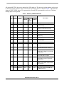
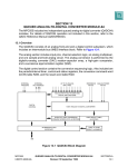
Freescale Semiconductor Device Errata Document Number: MCF5282DE Rev. 4, 9/2008 MCF5282 Device Errata Supports: MCF5281 and MCF5282 By: Microcontroller Solutions Group This document identifies implementation differences between the MCF5282 processor and the description contained in the MCF5282 ColdFire® Microcontroller User’s Manual. Refer to http://freescale.com/coldfire for the latest updates. The errata items listed in this document (summarized in Table 1) describe differences from the following documents: • MCF5282 ColdFire Microcontroller User’s Manual • ColdFire Microprocessor Family Programmer’s Reference Manual 1 2 3 4 5 6 7 8 9 10 11 12 13 14 15 16 17 18 © Freescale Semiconductor, Inc., 2008. All rights reserved. Leakage Current on VDDPLL pin . . . . . . . . . . . . . . . . . . . 3 BDM Load of SR Does Not Enable Stack Pointer . . . . . . 3 Unexpected Pipeline Stall on EMAC Load/Store Accumulator Instruction . . . . . . . . . . . . . . . . . . . . . . . . . . . . . . . . . 3 Incorrect Cache Size . . . . . . . . . . . . . . . . . . . . . . . . . . . . 4 Corrupted Fetches from Flash. . . . . . . . . . . . . . . . . . . . . 4 Possible Cache Corruption After Setting CACR[CINV] . 5 Incorrect Operation of CACR[CFRZ] . . . . . . . . . . . . . . . 5 Incorrect 32-bit Accesses to FlexCAN Registers. . . . . . . 6 FEC Receive Buffer Overrun in 10BaseT Mode . . . . . . . 6 Concantenation of Received Frames in 10BaseT Mode . 7 PLL Does Not Lock in Normal PLL Mode with External Clock Reference . . . . . . . . . . . . . . . . . . . . . . . . . . . . . . . 8 Interrupts Do Not Trigger on Consecutive Transmit . . . . 8 Possible QADC Command Conversion Word (CCW) Table Corruption . . . . . . . . . . . . . . . . . . . . . . . . . . . . . . . . . . . . 9 GPIO Inputs Behave Inappropriately. . . . . . . . . . . . . . . 10 Phase Relationship Between CLKOUT and CLKIN Not Preserved When Using PLL . . . . . . . . . . . . . . . . . . . . . . . . 10 FEC Duplicate Transmission Bug . . . . . . . . . . . . . . . . . 10 FlexCAN Writing to an Active Receive MB May Corrupt MB Contents . . . . . . . . . . . . . . . . . . . . . . . . . . . . . . . . . . . . 11 Revision History. . . . . . . . . . . . . . . . . . . . . . . . . . . . . . . 12 All current MCF5282 devices are marked as L95M mask set. The date code on the marking can be used to determine which errata have been corrected on a particular device as shown in Table 1. The datecode format is XXXYYWW, where YY represents the year and WW represents the work week. The three leading digits can be ignored. Table 1. Summary of MCF5282 Errata Date Code Affected Errata Module Date Errata ID Affected Added <XXX0324 XXX0324 to XXX0327 XXX0326 Errata Title 1 PLL 03/18/03 Yes No No Leakage current on VDDPLL pin 2 BDM 03/28/03 Yes Yes Yes BDM load of SR does not enable stack pointer exchange 3 EMAC 03/28/03 Yes Yes No Unexpected pipeline stall on EMAC load/store accumulator instruction 4 Cache 03/31/03 Yes Yes No Incorrect cache size 5 Flash 04/09/03 Yes Yes No Corrupted fetches from Flash 6 Cache 07/21/03 Yes Yes Yes Possible cache corruption after setting CACR[CINV] 7 Cache 07/21/03 Yes Yes Yes Incorrect operation of CACR[CFRZ] 8 FlexCAN 07/23/03 Yes Yes Yes 32-bit accesses to FlexCAN registers do not work properly 9 FEC 04/22/04 Yes Yes Yes FEC receive buffer overrun in 10baseT 10 FEC 04/22/04 Yes Yes Yes Concantenation of received frames in 10baseT 11 PLL 08/23/04 Yes Yes Yes PLL does not lock when in normal PLL mode with external clock reference 12 FEC 09/14/04 Yes Yes Yes Late collision, retry limit, and underrun interrupts do not trigger on consecutive transmit frames 13 QADC 03/15/05 Yes Yes Yes Possible QADC Command Conversion Word (CCW) table corruption 14 GPIO 01/06/06 Yes Yes Yes GPIO inputs behave inappropriately when pull-down resistors larger than 10k are used 15 PLL 06/12/06 Yes Yes Yes The phase relationship between CLKOUT and CLKIN is not preserved when using PLL 16 FEC 05/31/07 Yes Yes Yes FEC duplicate transmission bug FlexCAN 08/28/08 Yes Yes Yes Writing to an active receive MB may corrupt MB contents MCF5282 Device Errata, Rev. 4 2 Freescale Semiconductor Leakage Current on VDDPLL pin 1 Leakage Current on VDDPLL pin 1.1 Description The MCF5282 exhibits a 65mA leakage current on the VDDPLL supply, regardless of chip configuration. 1.2 Workaround No workaround. XXX0323 and earlier datecodes are affected. 2 BDM Load of SR Does Not Enable Stack Pointer Exchange 2.1 Description The V2 core used in the MCF5282 adds support for separate user and supervisor stack pointers. The hardware implements an active stack pointer and an “other_stack_pointer. Whenever the operating mode of the processor changes (supervisor user, user supervisor), the processor hardware exchanges the active SP and the other SP. This exchange operation does not work when the processor mode is changed by a write to the SR from the BDM port. The hardware in the processor core required to process the BDM load_SR operation and enable the stack pointer exchange is missing. The exchange works properly when the SR is changed through software. 2.2 Workaround Use software for any operations that require exchanging the stack pointers. All datecodes are affected. 3 Unexpected Pipeline Stall on EMAC Load/Store Accumulator Instruction 3.1 Description An unexpected pipeline stall occurs for accumulator load and accumulator store instructions that immediately follow a load accumulator or MAC instruction. MCF5282 Device Errata, Rev. 4 Freescale Semiconductor 3 Incorrect Cache Size Specifically, the operand execution pipeline (OEP) experiences a 2T pipeline stall when a load/store accumulator instruction enters the pipeline immediately after any load accumulator or MAC instruction. The pipeline is supposed to stall only if there is a store accumulator instruction immediately following a load or MAC instruction that updated the specified accumulator. A simple example can be created to expose this problem: mac.l ra,rb,acc0 mac.l rc,rd,acc0 mov.l acc1,rx In the above example, the store of acc1 (mov.l acc1,rx) should not experience any stall because that accumulator is not being updated. In the current V2 + EMAC implementation, it incorrectly stalls for two cycles. NOTE The operation of the instructions is correct. The problem is that the expected timing is not met. 3.2 Workaround No workaround. XXX0326 and earlier datecodes are affected. 4 Incorrect Cache Size 4.1 Description The MCF5282 operates as if it were connected to an 8KB cache; however, the cache size is in fact 2KB. After the 2KB cache is full, the cache controller can have erroneous hits in the cache space resulting in data and/or instruction corruption. 4.2 Workaround Do not enable the cache. XXX0326 and earlier datecodes are affected. 5 Corrupted Fetches from Flash 5.1 Description Leaving bit 6 in the FLASHBAR register cleared can cause corrupted fetches from the MCF5282’s internal Flash. For datecodes after XXX0327, the bit is hardwired high to prevent the corrupted accesses. MCF5282 Device Errata, Rev. 4 4 Freescale Semiconductor Possible Cache Corruption After Setting CACR[CINV] 5.2 Workaround Set bit 6 in the FLASHBAR. This prevents the corrupted fetches. XXX0326 and earlier datecodes are affected. 6 Possible Cache Corruption After Setting CACR[CINV] 6.1 Description The cache on the MCF5282 was enhanced to function as a unified data and instruction cache, an instruction cache, or an operand cache. The cache function and organization is controlled by the cache control register (CACR). The CINV (Bit 24 = cache invalidate) bit in the CACR causes a cache clear. If the cache is configured as a unified cache and the CINV bit is set, the scope of the cache clear is controlled by two other bits in the CACR, INVI (BIT 21 = CINV instruction cache only) and INVD (BIT 20 = CINV data cache only). These bits allow the entire cache, the instruction portion of the cache, or the data portion of the cache to be cleared. If a write to the CACR is performed to clear the cache (CINV = BIT 24 set) and only a partial clear is done (INVI = BIT 21 or INVD = BIT20 set), cache corruption may occur. 6.2 Workaround All loads of the CACR that perform a cache clear operation (CINV = BIT 24) should be followed immediately by a NOP instruction. This avoids the cache corruption problem. All datecodes are affected. 7 Incorrect Operation of CACR[CFRZ] 7.1 Description The cache on the ColdFire V2 is controlled by the cache control register (CACR). When CACR[CFRZ] is set, the cache freeze function is enabled and no valid cache array entry is displaced. However, this feature does not work as specified, sometimes allowing valid lines to be displaced when CACR[CFRZ] is enabled. This does not cause any corrupted accesses. However, there could be cache misses for data that was originally loaded into the cache but was subsequently deallocated even though the CACR[CFRZ] bit was set. Also, incoherent cache states are possible when a frozen cache is cleared via the CINV (bit 24 = cache invalidate) bit in the CACR. MCF5282 Device Errata, Rev. 4 Freescale Semiconductor 5 Incorrect 32-bit Accesses to FlexCAN Registers 7.2 • • Workaround Unfreeze the cache by clearing CACR[CFRZ] when invalidating the cache using the CACR[CINV] bit. Use the internal SRAM to store critical code/data if the system cannot handle a potential cache miss. All datecodes are affected. 8 Incorrect 32-bit Accesses to FlexCAN Registers 8.1 Description Because the FlexCAN was originally designed for 16-bit architectures, all 32-bit register accesses are broken down into two back-to-back 16-bit accesses. However, the timing for the back-to-back accesses is incorrect and leads to corruption of the second 16-bit read or write. 8.2 Workaround When reading or writing to the 32-bit RxMASK registers, use two 16-bit accesses instead of a single 32-bit access. All datecodes are affected. 9 FEC Receive Buffer Overrun in 10BaseT Mode 9.1 Description When the FEC is connected to a 10BaseT network, if length of the data stored in a descriptor is not evenly divisible by 16 (not line-aligned), the FEC writes extra lines at the end of the buffer. The entire line that contains the last valid data is written and at least one extra line, but up to four lines after the end of the valid data can also be written. In most cases, this is not a problem because the extra lines of data continue falling within the limits of the buffer. However, if the valid data ends near the end of the buffer, the extra lines written by the FEC might be outside of the data buffer. This leads to corruption of the next buffer, descriptor, data, or code stored in the adjacent memory. For example, as shown in Figure 1, if the max buffer size is programmed to 0x600 and a frame that is 0x5F8 bytes long is received, a line is written starting at buffer start + 0x5F0. The first half of the line at buffer start + 0x5F0 is valid frame data that should be processed by the FEC driver; the second half of the line is additional data that is written because the FEC only writes complete lines. This data should be ignored by the FEC driver. So far, this is correct FEC behavior as originally specified. However, the FEC repeats the last line of valid data a number of times. The line at buffer start + 0x600 is written, and as many as three additional lines beyond the end of the data buffer could be written. MCF5282 Device Errata, Rev. 4 6 Freescale Semiconductor Concantenation of Received Frames in 10BaseT Mode buffer start + 0x5E0 buffer start + 0x5F0 End of data buffer buffer start + 0x600 buffer start + 0x610 Valid frame data buffer start + 0x620 Expected extra data buffer start + 0x630 Unexpected data/ overflows the data buffer Figure 1. Buffer Overrun Example 9.2 Workaround There are three independent workarounds: 1. Only use 100BaseT. 2. Allocate extra lines for the receive data buffers. The actual allocated memory for each buffer should be equal to the receive buffer size programmed in the FEC’s EMRBR register plus four lines (16 byte-sized lines). 3. Program the data buffer size one line larger than the max packet size (data buffer size = EMRBR + 0x40). All datecodes are affected. 10 Concantenation of Received Frames in 10BaseT Mode 10.1 Description When the FEC is connected to a 10BaseT network, sometimes the FEC combines the data from multiple frames to generate a single frame. The data from the frames is received correctly, but the frame boundary is not reported correctly. This causes the descriptor to report the length as the data length for all of the concantenated frames added together. The incorrect data length might exceed the max frame length programmed in the RCR[MAX_FL] field. When TCP is used as a transport mechanism, this errata manifests itself as lost packets and reduced throughput. Data continues to be received correctly because TCP requests retransmission of bad packets. However, UDP does not include any mechanism for packet retransmission, as it is a send and forget protocol. Consequently, while UDP should be able to identify an incorrectly received packet (because its checksum will fail), higher level software in the protocol stack must be capable of requesting retransmission to work around this errata. MCF5282 Device Errata, Rev. 4 Freescale Semiconductor 7 PLL Does Not Lock in Normal PLL Mode with External Clock Reference 10.2 Workaround Higher level Ethernet layer code should compare the length reported by the descriptor to the length included in its header. If the lengths do not match, the packet should be truncated or discarded as needed. The protocol stack must be responsible for requesting retransmission of any frames that are discarded due to the data length mismatch. All datecodes are affected. 11 PLL Does Not Lock in Normal PLL Mode with External Clock Reference 11.1 Description During a power on reset, if the CLKMOD[1:0] equals 10 setting is used (normal PLL mode with external clock reference), the MCF5282 PLL does not lock and the device never comes out of reset. 11.2 Workaround When configuring the PLL for normal PLL mode with external clock reference, tie CLKMOD1 to RSTI and not straight to 3.3V. This allows the PLL to correctly detect the desired operating mode and lock. All datecodes are affected. 12 Interrupts Do Not Trigger on Consecutive Transmit Frames 12.1 Description The late collision (LC), retry limit (RL), and underrun (UN) interrupts do not trigger on consecutive transmit frames. For example, if back-to-back frames cause a transmit underrun, only the first frame generates an underrun interrupt. No other underrun interrupts are generated until a frame is transmitted that does not underrun or the FEC is reset. 12.2 Workaround Because late collision, retry limit, and underrun errors are not directly correlated to a specific transmit frame, in most cases a workaround for this problem is not needed. If a workaround is required, there are two independent workarounds: • Ensure that a correct frame is transmitted after a late collision, retry limit, or underrun errors are detected. MCF5282 Device Errata, Rev. 4 8 Freescale Semiconductor Possible QADC Command Conversion Word (CCW) Table Corruption • Perform a soft reset of the FEC by setting ECR[RESET] when a late collision, retry limit, or underrun errors are detected. DATECODES AFFECTED: All 13 Possible QADC Command Conversion Word (CCW) Table Corruption 13.1 Description A CCW Table location may be corrupted by writing any other CCW or Results table location while any Queue is active. If a CCW table or result table write occurs while either queue is active, it is possible for another CCW location to be corrupted. This bug only occurs if the write cycle is simultaneous with the queue state machine reading the next CCW location. The odds of this happening are 1 in the number of clocks in a conversion. 13.2 Workaround There are three possible workarounds: 1. Make sure that both queues have completed or are paused before updating a CCW table or result table location. 2. If workaround one is not possible, the application code can monitor the CWP bits in the QASR0. After it changes, it is safe to write a CCW Table or Result Register location. The safe time is equal to the input sample time of the next conversion (4-18 QCLKs). 3. If workarounds one and two are not possible, it is possible to update a CCW or Result Register location while a queue is active by going through the following sequence: — Read Status Register 0 and save the CWP value — Perform the write — Read CCW locations pointed to by CWP and CWP+1 to check if they are corrupted — Fix any of the possibly corrupted locations The above sequence should be safe. If a CCW location is corrupted, it is not used until a queue wraps around back to this CCW. The user has one conversion time to perform the corruption checks and fixes. There should be plenty of time to do this without worrying about another CCW corruption. MCF5282 Device Errata, Rev. 4 Freescale Semiconductor 9 GPIO Inputs Behave Inappropriately 14 GPIO Inputs Behave Inappropriately 14.1 Description GPIO inputs that shouldn't have internal pull-ups, behave as if internal pull-ups are enabled when pull-down resistors larger than 10k are used To achieve 5V tolerance for the I/O pads, a pull-up device is used to latch the input value of the pads while protecting internal circuitry to direct exposure to potentials above 3.6V. These pull-up devices are not disabled after stimulus is removed and a pull-down resistor value larger than 10k is used. 14.2 Workaround To disable the pull-up, a pull-down resistor value of 10k or less is needed. DATECODES AFFECTED: All 15 Phase Relationship Between CLKOUT and CLKIN Not Preserved When Using PLL 15.1 Description In all PLL modes, the CLKOUT phase relationship to the input clock drifts by 25-33%. 15.2 Workaround Use bypass mode; set CLKMOD[1:0] bits to 00. The CLKOUT to CLKIN phase relationship is maintained. DATECODES AFFECTED: All 16 FEC Duplicate Transmission Bug 16.1 Description In some cases, the FEC transmits single frames more than once. The FEC fetches transmit buffer descriptors (TxBDs) and the corresponding Tx data continuously until the Tx FIFO is full. It does not determine whether the TxBD to be fetched is already being processed internally (as a result of a wrap). As the FEC nears the end of the transmission of one frame, it begins to DMA the data for the next frame. To remain one BD ahead of the DMA, it also fetches the TxBD for the next frame. It is possible that the FEC fetches from memory a BD that has already been processed but not yet written back (it is read a second time with the R bit set). In this case, the data is fetched and transmitted again. MCF5282 Device Errata, Rev. 4 10 Freescale Semiconductor FlexCAN Writing to an Active Receive MB May Corrupt MB Contents 16.2 Workaround Using at least three TxBDs fixes this problem for large frames, but not for small frames. To ensure correct operation for large or small frames, one of the following must be true: • The FEC software driver ensures that there is always at least one TxBD with the Ready bit cleared. • Every frame uses more than one TxBD and every TxBD, but the last is written back immediately after the data is fetched. The FEC software driver ensures a minimum frame size, n. The minimum number of TxBDs is then rounded up to the nearest integer (though the result cannot be less than 3). The default Tx FIFO size is 192 Bytes; this size is programmable. 17 FlexCAN Writing to an Active Receive MB May Corrupt MB Contents 17.1 Description Deactivating a FlexCAN receive message buffer (MB) may cause corruption of another active receive MB, including the ID field, if the following sequence occurs. 1. A receive MB is locked via reading the control/status word, and has a pending frame in the temporary receive serial message buffer (SMB). 2. A second frame is received that matches a second receive MB, and is queued in the second SMB. 3. The first MB is unlocked during the time between receiving the CRC field and the sixth bit of end of frame (EOF) of the second frame. 4. The second MB is deactivated within nine bus clock cycles of the sixth bit of EOF, resulting in corruption of the first MB. During standard use of the FlexCAN hardware, the errata can appear during heavy communications with several Rx MBs at a low baudrate and while using Rx extended MB’s IDs. This can be easily observed by checking ID value overwrite. In all cases, CAN transmissions from the processor are not affected at any moment. 17.2 Workaround 1. Do not write to the control/status word after initializing a receive MB. If a write (deactivation) is required to the control/status field of an active receive MB, either freeze the FlexCAN module or insert a delay of at least 27 CAN bit times plus 10 bus clock cycles between unlocking one MB and deactivating another MB. This avoids MB corruption; however, frames may still be lost. 2. The FlexCAN software driver ensures IDs are not changed during each reception. As soon as it has changed, return to original value. DATECODES AFFECTED: All MCF5282 Device Errata, Rev. 4 Freescale Semiconductor 11 Revision History 18 Revision History Table 2 provides a revision history for this document. Table 2. MCF5282DE Document Revision History Rev. No. Substantive Change(s) 3 Added errata: • Section 15, “Phase Relationship Between CLKOUT and CLKIN Not Preserved When Using PLL” • Section 16, “FEC Duplicate Transmission Bug” 4 Added errata: • Section 15, “Phase Relationship Between CLKOUT and CLKIN Not Preserved When Using PLL MCF5282 Device Errata, Rev. 4 12 Freescale Semiconductor How to Reach Us: Home Page: www.freescale.com E-mail: [email protected] USA/Europe or Locations Not Listed: Freescale Semiconductor Technical Information Center, CH370 1300 N. Alma School Road Chandler, Arizona 85224 +1-800-521-6274 or +1-480-768-2130 [email protected] Europe, Middle East, and Africa: Freescale Halbleiter Deutschland GmbH Technical Information Center Schatzbogen 7 81829 Muenchen, Germany +44 1296 380 456 (English) +46 8 52200080 (English) +49 89 92103 559 (German) +33 1 69 35 48 48 (French) [email protected] Japan: Freescale Semiconductor Japan Ltd. Headquarters ARCO Tower 15F 1-8-1, Shimo-Meguro, Meguro-ku, Tokyo 153-0064, Japan 0120 191014 or +81 3 5437 9125 [email protected] Asia/Pacific: Freescale Semiconductor Hong Kong Ltd. Technical Information Center 2 Dai King Street Tai Po Industrial Estate Tai Po, N.T., Hong Kong +800 2666 8080 [email protected] For Literature Requests Only: Freescale Semiconductor Literature Distribution Center P.O. Box 5405 Denver, Colorado 80217 1-800-441-2447 or 303-675-2140 Fax: 303-675-2150 [email protected] Information in this document is provided solely to enable system and software implementers to use Freescale Semiconductor products. There are no express or implied copyright licenses granted hereunder to design or fabricate any integrated circuits or integrated circuits based on the information in this document. Freescale Semiconductor reserves the right to make changes without further notice to any products herein. Freescale Semiconductor makes no warranty, representation or guarantee regarding the suitability of its products for any particular purpose, nor does Freescale Semiconductor assume any liability arising out of the application or use of any product or circuit, and specifically disclaims any and all liability, including without limitation consequential or incidental damages. “Typical” parameters that may be provided in Freescale Semiconductor data sheets and/or specifications can and do vary in different applications and actual performance may vary over time. All operating parameters, including “Typicals”, must be validated for each customer application by customer’s technical experts. Freescale Semiconductor does not convey any license under its patent rights nor the rights of others. Freescale Semiconductor products are not designed, intended, or authorized for use as components in systems intended for surgical implant into the body, or other applications intended to support or sustain life, or for any other application in which the failure of the Freescale Semiconductor product could create a situation where personal injury or death may occur. Should Buyer purchase or use Freescale Semiconductor products for any such unintended or unauthorized application, Buyer shall indemnify and hold Freescale Semiconductor and its officers, employees, subsidiaries, affiliates, and distributors harmless against all claims, costs, damages, and expenses, and reasonable attorney fees arising out of, directly or indirectly, any claim of personal injury or death associated with such unintended or unauthorized use, even if such claim alleges that Freescale Semiconductor was negligent regarding the design or manufacture of the part. Freescale™ and the Freescale logo are trademarks of Freescale Semiconductor, Inc. All other product or service names are the property of their respective owners.© Freescale Semiconductor, Inc. 2008. All rights reserved. MCF5282DE Rev. 4 9/2008