1
KIT-V850E/GP1-NBD
USER'S MANUAL (REV. 1.00)
Midas lab.
KIT-V850E/GP1-NBD
USER'S MANUAL (REV. 1.00)
♦ Upgrading version of software
• The newest version of RTE for Win32 (Rte4win32) can be downloaded from the following site:
http://www.midas.co.jp/products/download/program/rte4win_32.htm
♦ Cautions
• Midas lab Inc. possesses all copyrights of KIT-V850E/GP1-NBD (programs and manuals).
• These programs and manuals are protected by the Copyright Act and must not be copied, transcribed, or
revised without written permission from Midas lab Inc.
• You will be given a permission to use only one system per license. Two or more systems cannot be used
with one license.
• All precautions are taken in producing this product. Midas lab Inc. and its distributors do not assume any
responsibility for the result of using this product.
• The contents of this program and manual are subject to change without notice.
♦ Trademarks
• MS-Windows, Windows, MS, and MS-DOS are trademarks of Microsoft Corporation.
The names of the other programs, systems, and CPUs mentioned in this document are the trademarks of
the respective manufacturers.
1
KIT-V850E/GP1-NBD
USER'S MANUAL (REV. 1.00)
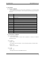
REVISION HISTORY
Date of application
July 21, 2002
Revision
1.00
Chapter
Description
Official first edition
2
KIT-V850E/GP1-NBD
USER'S MANUAL (REV. 1.00)
CONTENTS
1. OVERVIEW .................................................................................................................................... 5
2. MAIN FEATURES .......................................................................................................................... 5
3. UNPACKING AND CHECKING THE CONTENTS........................................................................ 6
4. ABOUT THE NBD.......................................................................................................................... 7
4.1.
OUTLINE ................................................................................................................................................7
4.2.
NBD FUNCTIONS ..................................................................................................................................7
5. HARDWARE SPECIFICATIONS ................................................................................................... 7
6. SYSTEM CONFIGURATION ......................................................................................................... 8
7. COMPONENT NAMES AND FUNCTIONS ................................................................................... 9
8. INSTALLATION PROCEDURE ................................................................................................... 10
9. CONNECTION TO THE USER SYSTEM .................................................................................... 11
9.1.
POWERING ON AND OFF...................................................................................................................11
10.
RTE for WIN32 ......................................................................................................................... 12
10.1.
11.
SELECTING RTE..............................................................................................................................12
PRECAUTIONS ........................................................................................................................ 14
11.1.
PRECAUTIONS RELATED TO OPERATION ...................................................................................14
11.2.
PRECAUTIONS RELATING TO THE USE OF THE NBD.................................................................14
12.
CONNECTOR SPECIFICATIONS ............................................................................................ 15
12.1.
POWER JACK ..................................................................................................................................15
12.2.
EXT CONNECTOR ...........................................................................................................................15
12.3.
NBD CONNECTOR...........................................................................................................................16
13.
DATA OUT CONNECTOR........................................................................................................ 17
14.
SOFTWARE CONFIGURATION .............................................................................................. 19
15.
LINE COMMAND ...................................................................................................................... 20
15.1.
AVAILABLE COMMANDS.................................................................................................................20
15.2.
DESCRIPTION OF COMMANDS......................................................................................................20
15.2.1.
Numeric Representation ............................................................................................................20
15.2.2.
HELP (?) ....................................................................................................................................20
15.2.3.
VER............................................................................................................................................20
3
KIT-V850E/GP1-NBD
USER'S MANUAL (REV. 1.00)
15.2.4.
NBDENV ....................................................................................................................................21
15.2.5.
ACC ...........................................................................................................................................21
15.2.6.
SYMFILE....................................................................................................................................21
15.2.7.
SYM ...........................................................................................................................................21
15.2.8.
ntp ..............................................................................................................................................21
15.2.9.
FREAD/TREAD..........................................................................................................................22
15.2.10.
FWRITE/TWRITE ......................................................................................................................22
15.2.11.
FDASM/TDASM .........................................................................................................................23
15.2.12.
FFILL..........................................................................................................................................23
15.2.13.
FSAVE/TSAVE ..........................................................................................................................23
15.2.14.
FLOAD/TLOAD ..........................................................................................................................24
15.2.15.
TMAP .........................................................................................................................................24
15.2.16.
TCOPY.......................................................................................................................................24
15.3.
BATCH FILE .....................................................................................................................................25
15.4.
NOTES..............................................................................................................................................25
4
KIT-V850E/GP1-NBD
1.
USER'S MANUAL (REV. 1.00)
OVERVIEW
KIT-V850E/GP1-NBD is a kit packaging software that controls the NBD functions of the
V850E/GP1, and a dedicated cable.
To use this kit, the RTE-NBD2 optionally available is
necessary.
This document explains the functions and handling of the RTE-NBD2 when the RTE-NBD2 is
connected to the V850E/GP1.
2.
MAIN FEATURES
RAM monitoring
Data from multiple built-in RAM areas can be recorded without halting the execution of a running
program.
Data tuning for flash ROM
Tuning RAM replaces the data area of the flash ROM, thus allowing data tuning without rewriting
the flash ROM.
Event detection
An event detection function that allows the user to freely use the trigger of RAM monitor is
provided.
5
KIT-V850E/GP1-NBD
3.
USER'S MANUAL (REV. 1.00)
UNPACKING AND CHECKING THE CONTENTS
Unpack the delivered packages and make sure that none of the following components are
missing. If any of the components is missing or damaged, contact the retailer from whom you
purchased the product.
• 40-pin-16-pin flat cable
• 10-pin-10-pin flat cable
• RTE for WIN32 Setup Disk (CD-ROM)
• NBD Manager Setup Disk
• User's Manuals (one set for each)
• License setting sheet
The following are general-purpose products that are required to use the KIT-V850E/GP1-NBD,
although they are not supplied with the product.
• RTE-NBD2 set
• Interface kit (interface card and cable)
One of the following interface kits is needed:
• PC Card interface kit
• PC98 Series Host Card (C bus) interface kit
• PC/AT compatible Host Card (ISA bus) interface kit
• PC/AT compatible Host Card (PCI bus) interface kit
6
KIT-V850E/GP1-NBD
4.
USER'S MANUAL (REV. 1.00)
ABOUT THE NBD
4.1.
OUTLINE
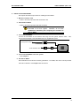
NBD stands for "Non-Break Debug" and supplies a function to access the internal resources of
the CPU while the CPU is under execution. The NBD is connected to an external CPU with 10 or so
signal lines.
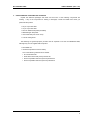
The following figure illustrates how the NBD is used.
CPU
RTE-NBD2
NBD
NBD- bus
4.2.
NBD FUNCTIONS
The V850E/GP1 provides the following NBD functions.
* RAM monitoring
* Flash ROM reading (evaluation chip only)
* Event detection (disabled when ICE is connected)
* Tuning RAM (evaluation chip only)
* Peripheral I/O register reading (disabled when ICE is connected)
5.
HARDWARE SPECIFICATIONS
The following table gives the specifications of the RTE-NBD2 when it is connected to the
V850E/GP1.
CPU to be debugged
V850E/GP1
RAM monitoring functions
Memory area that can be monitored
Number of channels
Memory monitoring unit
Maximum number of channels that can be recorded
Specifiable triggers
Other
RAM area built in the CPU
64 channels
Byte, half-word, or word
16 K channels
Interval time, event, and external signal
Real-time data output
Tuning RAM functions
Replaceable memory area
RAM size
ROM area built into the CPU
4 KB * 8 areas
Event functions
Number of events
Status
Address conditions
External output
Operating voltage
1
Write, execute
26 bits
Supported
+3 to +5 V
7
KIT-V850E/GP1-NBD
6.
USER'S MANUAL (REV. 1.00)
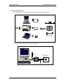
SYSTEM CONFIGURATION
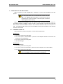
The following figure shows the system configuration in which the RTE-NBD2 is used.
Windows 95 or Windows NT
PC98 Series PC interface card
PC98 Series PC
NBD Manager
AC adapter (power)
PC/AT interface card
(ISA & PCI)
PC/AT compatible PC
Host system interface cable
(supplied with the interface
card)
RTE-NBD2
40-pin-16-pin flat cable
(for user system connection)
PC Card interface
Note-type PC with a PC Card slot
The following figure shows how the devices are connected.
PC
AC adapter
NBD connector
RTE-NBD2
V850E/GP1
V850
User system
User system connection cable
8
KIT-V850E/GP1-NBD
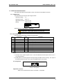
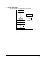
COMPONENT NAMES AND FUNCTIONS
This chapter shows the appearance of the RTE-NBD2, as well as the names and functions of its
components.
PC (host system) connector
User system connector
RAM monitor output connector
Pow er jack
5V
GND
HOST
DATA OUT
EXT
NBD IF
TOOL
NBD
7.
USER'S MANUAL (REV. 1.00)
EXT connector
TOOL/NBD user system pow er LED
Power jack
This is a connector for power supply. For the power specifications, see Section 12.1.
Do not connect any device other than the supplied AC
adapter (RTE-PS03) to the power jack.
PC (host system) connector (HOST)
This connector is used for connecting the RTE-NBD2 to the PC (host system). The host
system interface cable is connected to this connector.
EXT connector (EXT)
This connector is used for external signal input and internal signal output. For details, see
Section 12.2.
User system connector (NBD IF)
This connector is used for connecting the RTE-NBD2 to the user system. The RTE-NBD2
connector is a 40-pin connector that used only 16 pins. For details, see Section 12.3.
RAM monitor output connector (DATA OUT)
This connector provides a real-time output for the RAM monitor data. It is used for storing the
data in an external device. For details, see Chapter 13.
Power LED (POWER)
This LED lights steadily while the power to the RTE-NBD2 is on.
NBD user system power LED (NBD)
This LED lights steadily while the NBD is connected to the user system and the power to the
user system is on.
9
KIT-V850E/GP1-NBD
8.
USER'S MANUAL (REV. 1.00)
INSTALLATION PROCEDURE
This chapter describes the procedure for installing the RTE-NBD2.
1. Mount the interface card.
→ Refer to the manual provided with the interface card.
2. Install RTE for WIN32.
→ Refer to the manual provided with RTE for WIN32.
Unlike ICEs, the RTE-NBD2 does not operate until it is
connected to the user system. Therefore, do not start
ChkRTE2.exe immediately after completing the installation of
RTE for WIN32.
3. Connect the RTE-NBD2.
Connect the RTE-NBD2 to the interface card using the host system interface cable.
Also,
connect the AD adapter to the RTE-NBD2 when it is supplied with power.
To AC power source
To the interface card
4. Connect the RTE-NBD2 to the user system.
→ See Chapter 9.
5. Set RTE for WIN32.
Start ChkRTE2.exe and set the necessary parameters. For details, refer to the manual provided
with RTE for WIN32 or see Chapter 10 of this manual.
10
KIT-V850E/GP1-NBD
9.
USER'S MANUAL (REV. 1.00)
CONNECTION TO THE USER SYSTEM
Use the 40-pin-16-pin cable supplied as an accessory to connect the RTE-NBD2 to the user
system.
The user system must have a connector that connects the RTENBD.
See Section 12.3 and prepare a connector that can be
connected to the 16-pin connector of the user system connection
cable supplied as an accessory.
When connecting the RTE-NBD2 to the user system to which an ICE is connected, a 10-pin-10pin cable is necessary in addition to the above cable. Connect the EXT connector of the ICE to the
EXT connector of the RTE-NBD2. Check if 7 of the switch of the ICE is OFF; if it is ON, set it to
OFF. This arbitrates NBD access by the ICE and NBD access by the RTE-NBD2, so that both the
accesses can be used.
9.1.
POWERING ON AND OFF
The procedures for powering the system on and off are described below.
Powering on
1. Turn on the power to the host system.
2. Turn on the power to the RTE-NBD2. (Connect the AC adapter dedicated to the RTE to the
power jack of the RTE-NBD2.)
3. Turn on the power to the user system.
4. Start NBD Manager.
Powering off
1. Quit NBD Manager.
2. Turn off the power to the user system.
3. Turn off the power to the RTE-NBD2. (Disconnect the AC adapter from the RTE-NBD2.)
4. Turn off the power to the host system.
Do not turn on the power to the user system before powering
on the RTE-NBD2. Doing so may cause a malfunction.
11
KIT-V850E/GP1-NBD
10.
USER'S MANUAL (REV. 1.00)
RTE for WIN32
This chapter describes the setting and operation of RTE for WIN32, with the focus on the aspects
specific to the RTE-NBD2. ChkRTE2.exe is used to check the RTE for WIN32 setting and the RTENBD2 connection.
The function test of ChkRTE2.exe cannot be used unless the
RTE-NBD2 and the user system are properly connected and
the power to the user system is on.
10.1.
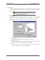
SELECTING RTE
After completing connection with the user system and turning on power to all the units, start
ChkRTE2.exe and perform environment setting of "RTE for WIN32".
Be sure to perform
environment setting of "RTE for WIN32" at least once when new hardware has been installed.
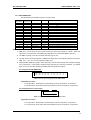
<Setting RTE>
<Selecting RTE>
Select V850E/GP1-NBD at the lower layer of NBD, from the product list.
<Selecting I/F-1 or I/F-2>
Select an interface suitable to the host interface to be used, from the pull-down menu (the
above screen shows, as an example, that ISA I/F card is specified).
<License>
Click this button, see the license setting sheet supplied with the kit, and perform license
setting. For details, refer to the manual of RTE for WIN32.
12
KIT-V850E/GP1-NBD
USER'S MANUAL (REV. 1.00)
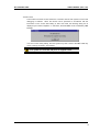
<Function test>
The function test cannot be done unless the connection with the user system is correct and
debugging is enabled.
When the function test is performed in accordance with the
instructions on the screen after setting of RTE was made, the following dialog box is
displayed upon normal completion. In this status, the RTE-NBD2 can be controlled by NBD
Manager.
If an error occurs during testing, the user system may have a fault or the NBD cable may
not be correctly connected. Check these.
Execute the function test of ChkRTE2.exe while the RTE-NBD2 and
user system are connected, and power is supplied to both.
13
KIT-V850E/GP1-NBD
USER'S MANUAL (REV. 1.00)
11. PRECAUTIONS
This chapter provides precautionary information about the use of the RTE-NBD2.
11.1. PRECAUTIONS RELATED TO OPERATION
1) Do not turn on the power to the user system when the power to the RTE-NBD2 is off. Doing so
may cause a malfunction.
2) Do not allow conductive material to fall through the vents of the RTE-NBD2 cabinet. Doing so
may cause a malfunction.
11.2. PRECAUTIONS RELATING TO THE USE OF THE NBD
1) When the CPU of the user system is connected to the ICE, functions other than the one to access
the internal RAM cannot be used.
2) If reset or power failure is effected from the user system, all the contents, including the setting of
events and tuning RAM, will be lost and must be set again.
14
KIT-V850E/GP1-NBD
USER'S MANUAL (REV. 1.00)
12. CONNECTOR SPECIFICATIONS
This chapter describes the specifications of the connectors for RTE-NBD2 connection.
12.1. POWER JACK
The specifications of the power jack are given below.
Operating voltage:
5V
Operating current:
Max. 2 A
Applicable connector: Type A (Φ 5.5)
Polarity:
Center ground
+5 V
GND
GND
+5 V
Applicable power supply device:
RTE-PS03
Do not connect any power supply device other than the
supplied AC adapter (RTE-PS03) to the power jack.
12.2. EXT CONNECTOR
The specifications of the EXT connector are given below.
Pin
number
Signal name
Input/
output
1
Reserved
--
2
SCAN_END
Output
Description
Leave this pin unconnected
Signal that goes high at the end of each RAM monitor scanNote 2
3
Reserved
--
4
NBD_TRG-
Output
Leave this pin unconnected
5
Reserved
--
6
no use
Leave this pin unconnected
7
no use
Leave this pin unconnected
8
no use
9
GND
--
10
RAMMON_EXT
Input
Low pulse signal output in response to an NBD event
Leave this pin unconnected
Leave this pin unconnected
Ground signal
External input signal for RAM monitor
Notes
1. The input circuit of these signals is of a 5 V-TTL level element and the output circuit is of OC. +
1-kΩ pull-up resistor.
2. SCAN_END is a low-level signal that is output during the RAM monitor scanning. The output of
this signal indicates the end of one cycle of the RAM monitor scan process.
Pin arrangement:
9
7
5
3
1
10
8
6
4
2
JEXT pin arrangement
Applicable connector:
XG4M-1031 manufactured by Omron Corporation, or equivalent
15
KIT-V850E/GP1-NBD
USER'S MANUAL (REV. 1.00)
12.3. NBD CONNECTOR
The specifications of the NBD connector are given below.
Pin number
(RTE-NBD2)
Pin number
(User system)
Signal name
Input/output
1
1
NBD_TRG-
Input
Connected to the TRIG_DBG terminal of the CPU.
2
2
NBD_VCC
Input
Connected to the power (3.3 V) of the user system.
3
NBD_OUT-
4
4
GND
5
5
NBD_CLK
6
6
GND
7
7
NBD_SYNC-
8
8
GND
9
9
NBD_DATA0
10
10
GND
11
11
NBD_DATA1
12
12
GND
13
13
NBD_DATA2
Input/output
Connected to the AD2_DBG terminal of the CPU.
14
14
NBD_DATA3
Input/output
Connected to the AD3_DBG terminal of the CPU.
15
15
MODE_DBG
Output
16
16
NBD_RESETO-
-Output
Usually not used.
Connected to the ground of the user system.
Connected to the CLK_DBG terminal of the CPU.
--
Connected to the ground of the user system.
Output
Connected to the SYNC terminal of the CPU.
-Input/output
-Input/output
--
Input
Reserved
Note 3
Note 1
3
17 to 40
Output
Description
Connected to the ground of the user system.
Connected to the AD0_DBG terminal of the CPU.
Connected to the ground of the user system.
Connected to the AD1_DBG terminal of the CPU.
Connected to the ground of the user system.
Connected to the MODE_NBD terminal of the CPU.
Connected to the RESETO_DBG terminal of the CPU. Note 4
Not used
Notes
1. NBD_OUT- is used when the user system stores input and output signals in a buffer. When the
signal is low, the signal flow of the bidirectional signal bus is from the RTE-NBD2 to the CPU.
2. The NBD connector is a 40-pin connector that used only 16 pins.
3. The high level of the output signal is a CMOS-level signal that is automatically limited to the level of
NBD_VCC. +3 to +5 V can be connected to NBD_VCC.
4. While the NBD_RESETO- signal is active (low level), monitor scanning and start condition sampling
are not performed. If this signal is asserted during scanning, the scanning is aborted. It is started
again as soon as the start condition is satisfied after the signal was cleared.
Pin arrangement (RTE-NBD2 side):
39 37 35 33 31
29 27 25 23 21 19 17 15 13 11
40 38 36 34 32 30
9
28 26 24 22 20 18 16 14 12 10
7
5
3
1
8
6
4
2
NBD connector pin arrangement (RTE-NBD2 side)
Applicable connector:
For 40-pin cable: XG4M-4030-T manufactured by Omron Corporation, or equivalent
For 40-pin board: XG4C-4031/4034 manufactured by Omron Corporation, or equivalent
Pin arrangement (user system side):
15 13 11
9
16 14 12 10
7
5
3
1
8
6
4
2
NBD connector pin arrangement (user system side)
Applicable connector:
For 16-pin cable: XG4M-1630-T manufactured by Omron Corporation, or equivalent
For 16-pin board: XG4C-1631/1634 manufactured by Omron Corporation, or equivalent
16
KIT-V850E/GP1-NBD
USER'S MANUAL (REV. 1.00)
13. DATA OUT CONNECTOR
The DATA OUT connector outputs the results of the RAM monitor scan in real time. The output
level of this signal is 5 V TTL. The specifications of the DATA OUT connector are given below.
Pin
number
Signal
name
1
GND
2
DLWP-
3
GND
4
DLDSTS
5
GND
6
Input/
output
Pin
number
Signal
name
Input/
output
--
21
GND
--
Output
22
DLD8
Output
--
23
DLD9
Output
Output
24
DLD10
Output
--
25
DLD11
Output
DLCH0
Output
26
DLD12
Output
7
DLCH1
Output
27
DLD13
Output
8
DLCH2
Output
28
DLD14
Output
9
DLCH3
Output
29
DLD15
Output
10
DLCH4
Output
30
GND
--
11
DLCH5
Output
31
NC
--
12
GND
--
32
NC
--
13
DLD0
Output
33
NC
--
14
DLD1
Output
34
NC
--
15
DLD2
Output
35
NC
--
16
DLD3
Output
36
NC
--
17
DLD4
Output
37
NC
--
18
DLD5
Output
38
NC
--
19
DLD6
Output
39
NC
--
20
DLD7
Output
40
NC
--
Signal name
Function
DLWP-
This signal is for data latch timing. When the channel size is set to Byte (8 bits) or
Half-word (16 bits), one DLWP- signal is output per channel. When the channel size
is set to Word (32 bits), two DLWP- signals are output per channel.
DLDSTS
This signal goes low when the output data of the DLD[15:0] signal is the low-order
16 bits. It goes high when the output data of the DLD[15:0] signal is the high-order
16 bits.
DLCH[5:0]
This signal indicates the channel number that is output to the DLD[15:0] signal.
DLD[15:0]
This signal contains the data that is read and output as a result of the scan. When
the channel size is set to Byte (8 bits), "0" is output to this signal. When the channel
size is set to Word (32 bits), two signals are output, one containing the low-order 16
bits and the other containing the high-order 16 bits.
t1
t2
DLWPDLDST
DLCH
DLD[15:0]
VALID
t3
Symbol
VALID
t4
Content
Interval
t1
Low pulse width of the DLWP- signal
Min. 30 ns
t2
High pulse width of the DLWP- signal
Min. 110 ns
t3
Setup time of the DLWP- signal
Min. 20 ns
t4
Hold time of the DLWP- signal
Min. 20 ns
17
KIT-V850E/GP1-NBD
USER'S MANUAL (REV. 1.00)
Pin arrangement:
39 37 35 33 31
29 27 25 23 21 19 17 15 13 11
40 38 36 34 32 30
9
28 26 24 22 20 18 16 14 12 10
7
5
3
1
8
6
4
2
DATA OUT connector pin arrangement
Applicable connector:
XG4M-4030-T manufactured by Omron Corporation, or equivalent
18
KIT-V850E/GP1-NBD
USER'S MANUAL (REV. 1.00)
14. SOFTWARE CONFIGURATION
The overall configuration of the software of this tool is as shown below.
NBD Manager
ChkRTE2.EXE
RTE for WIN32
RTE4W32.INI
NBD section
RTE-NBD2
NBD section
CPU
• RTE for WIN32 identifies the types of the connected hardware and I/O addresses from the
RTE4W32.INI file, which is created in the Windows directory.
• RTE4W32.INI is set by ChkRTE2.exe.
19
KIT-V850E/GP1-NBD
USER'S MANUAL (REV. 1.00)
15. LINE COMMAND
15.1. AVAILABLE COMMANDS
The line command is used on the command window of NBD Manager. The commands available
in the command window are listed below. All the commands are processed fly-by (non-break) vis-àvis the CPU.
Command name
Description
<
Executes a batch file.
HELP
Displays a list of commands.
?
VER
Displays the version.
NBDENV
Sets the environment (sets the cycle of NBD_CLK)
ACC
Allows the user to specify the access size.
SYMFILE
Reads a symbol file.
SYM
Displays symbol information.
ntp
Sets the trigger point
FREAD
Fly-by read
FWRITE
Fly-by write
FDASM
Disassembles the memory contents by means of fly-by read.
FFILL
Fills up the memory space by means of fly-by write.
FSAVE
Reads the memory contents by means of fly-by read and writes them into a file.
FLOAD
Reads the contents of a file and writes them into the memory space by means of fly-by write.
TREAD
Tuning RAM read
TWRITE
Tuning RAM write
TDASM
Disassembles the memory contents by means of tuning RAM read.
TSAVE
Reads the memory contents by means of tuning RAM read and writes them into a file.
TLOAD
Reads the contents of a file and writes them into the memory space by means of tuning RAM write.
TMAP
Specifies the tuning RAM allocation.
TCOPY
Copies the contents of flash-ROM to the tuning RAM.
15.2. DESCRIPTION OF COMMANDS
15.2.1. Numeric Representation
Unless otherwise specified, all numeric values of parameters of commands are handled as
hexadecimal numbers.
15.2.2. HELP (?)
<Format>
HELP
HELP displays a list of the commands. You may view this list by entering "?" instead of "HELP".
<Example> HELP
Displays a list of commands.
15.2.3. VER
<Format>
VER
VER displays the version of the RTE-NBD2 environment.
20
KIT-V850E/GP1-NBD
USER'S MANUAL (REV. 1.00)
15.2.4. NBDENV
<Format>
NBDENV [x1|x2|..x16]
NBDENV specifies the period of NBD_CLK.
On starting, a period in which CPU-ID can be correctly read is automatically set, with 80 ns (12.5
MHz) as the maximum frequency. x1..x16 specify a value of an integer multiple of period 40 ns.
<Example> x1 = 40 ns (25 MHz), x2 = 80 ns (12.5 MHz), x3 = 120 ns (8.333 MHz)…x16 = 640 ns
(1.5625 MHz)
15.2.5. ACC
<Format>
ACC [BYTE | HWORD | WORD]
ACC allows the user to specify the data size for access to memory. The FWRITE, TWRITE, and
FFILL commands observe the data size specified by the ACC command. If you omit the parameter
setting, the current setting is displayed.
<Example> ACC WORD
The memory access size is set to WORD (32 bits).
15.2.6. SYMFILE
<Format>
SYMFILE file_name
SYMFILE reads symbol information from a file that must be assigned for file_name. The file
format shall be ELF format in which GHS tool output is made. Symbols to be read shall be limited to
global symbols.
<Example> SYMFILE C:\TEST\TEST_PRO.ELF
15.2.7. SYM
<Format>
SYM string
SYM displays a symbol that corresponds to a character string that must be assigned for string.
<Example> SYM main
15.2.8. ntp
<Format>
NTP [address] [exec|write]
NTP sets a trigger points. exec specifies an executable address, and write specifies a write cycle
of a specified address.
<Example> NTP 3ff4000 write
21
KIT-V850E/GP1-NBD
USER'S MANUAL (REV. 1.00)
15.2.9. FREAD/TREAD
<Format>
FREAD [address [length]]
TREAD [address [length]]
FREAD/TREAD reads and displays the contents in a region whose range must be specified by
length, starting at an address that must be assigned for address.
The maximum value to be
assigned to length is 100 (0x100). By pressing Return in response to the prompt, however, the
display of the memory contents can be continued. If you omit the parameter setting, the most
recently set parameters are applied.
FREAD is a command that is used to access a space that can be viewed from the CPU. Only the
space permitted by the specifications of the CPU can be accessed.
TREAD is a command that is used to access only the tuning RAM. The tuning RAM in the area
allocated by TMAP as tram or hidden can be accessed.
<Example> FREAD 0 100
15.2.10. FWRITE/TWRITE
<Format>
FWRITE address data0[ data1[ data2[ data3...]]]]
TWRITE address data0[ data1[ data2[ data3...]]]]
FWRITE/TWRITE writes data0, data1, data2 ... begins at an address that must be assigned for
address. The data size for write shall be as set by the ACC command. Therefore, if the ACC
command setting is "WORD", an input of "FWRITE FF8000 1", for example, is evaluated with "1"
being "0x00000001".
FWRITE is a command that is used to access a space that can be viewed from the CPU. Only
the space permitted by the specifications of the CPU can be accessed.
TWRITE is a command that is used to access only the tuning RAM. The tuning RAM in the area
allocated by TMAP as tram or hidden can be accessed.
<Example> FWRITE ff8000 11 22 33 44
22
KIT-V850E/GP1-NBD
USER'S MANUAL (REV. 1.00)
15.2.11. FDASM/TDASM
<Format>
FDASM [address [length]]
TDASM [address [length]]
FDASM/TDASM displays the contents in a region whose range must be specified by length,
starting at an address that must be assigned for address. Regardless of the value assigned for
length, the display is terminated once twenty lines have been displayed. By pressing Return in
response to the prompt, however, display can be continued. If you omit the parameter setting, the
most recently set parameters are applied.
FDASM is a command that is used to access a space that can be viewed from the CPU. Only the
space permitted by the specifications of the CPU can be accessed.
TDASM is a command that is used to access only the tuning RAM. The tuning RAM in the area
allocated by TMAP as tram or hidden can be accessed.
<Example> FDASM 0 10
15.2.12. FFILL
<Format>
FFILL address length data
FFILL writes data into a whole region whose range must be specified by length, starting at an
address that must be assigned for address. The data size for write shall be as set by the ACC
command. Therefore, if the ACC command setting is "WORD", an input of "FFILL FF8000 10 1", for
example, is evaluated with "1" being "0x00000001".
FFILL is a command that is used to access a space that can be viewed from the CPU. Only the
space permitted by the specifications of the CPU can be accessed.
<Example> FFILL ff8000 10 55aa
15.2.13. FSAVE/TSAVE
<Format>
FSAVE address length file_name
TSAVE address length file_name
FSAVE/TSAVE reads a region whose range must be specified by length, starting at an address
that must be assigned for address, and writes the contents into a file that must be specified for
file_name.
FSAVE is a command that is used to access a space that can be viewed from the CPU. Only the
space permitted by the specifications of the CPU can be accessed.
TSAVE is a command that is used to access only the tuning RAM. The tuning RAM in the area
allocated by TMAP as tram or hidden can be accessed.
<Example> FSAVE ff8000 1000 c:\data1.bin
23
KIT-V850E/GP1-NBD
USER'S MANUAL (REV. 1.00)
15.2.14. FLOAD/TLOAD
<Format>
FLOAD address file_name
TLOAD address file_name
FLOAD/TLOAD downloads the contents of a file that must be specified for file_name to an
address that must be assigned for address.
FLOAD is a command that is used to access a space that can be viewed from the CPU. The
space permitted by the specifications of the CPU can be accessed.
TLOAD is a command that is used to access only the tuning RAM. The tuning RAM in the area
allocated by TMAP as tram or hidden can be accessed.
<Example> FLOAD ff8000 c:\data1.bin
15.2.15. TMAP
<Format>
TMAP [address length {flash|tram|hidden}]
TMAP allows the user to specify the tuning RAM allocation. The user may specify an address
length to which the tuning RAM is allocated. Up to eight blocks can be allocated as the tuning RAM
in 4-KB units.
An area of the tuning RAM allocated as tram can be accessed by fly-by access commands such
as FREAD and FWRITE, as well as by the CPU.
An area of the tuning RAM allocated as hidden can be accessed only by a command to the tuning
RAM (TREAD, TWRITE, …) while the executing CPU can view flash.
flash clears allocation of the tuning RAM and allocates flash ROM. This area of the tuning RAM
cannot be accessed by neither the CPU nor tool.
<Example> tmap 0 8000 tram
15.2.16. TCOPY
<Format>
TCOPY [address length|/all]
TCOPY copies the contents of the flash ROM within the address range in which the tuning RAM is
allocated and in the range specified by address length, to the tuning RAM. If /all is specified in the
place of address length, all the blocks allocated as tram and hidden are transferred.
<Example> tcopy 0 100
24
KIT-V850E/GP1-NBD
USER'S MANUAL (REV. 1.00)
15.3. BATCH FILE
The use of "<filename" format commands in a batch file is supported. Because a batch file is a text
format file, describe one command on one line.
A batch file is useful when commands are used repeatedly or when a series of commands shall be
executed, for instance, for initialization.
<Example> < RAMCHECK1.BAT
15.4. NOTES
• Entry shall be made from the prompt line, regardless of the cursor position.
• When the command window becomes active, the contents of the clipboard are cleared.
• Copy and paste are the only edit functions.
25
Memo
KIT-V850E/GP1-NBD USER'S MANUAL
M052MNL02
Midas lab
26