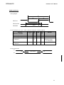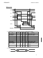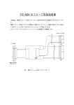
1
RTE-2000-TP
Hardware User's Manual
RealTimeEvaluator
RTE-2000-TP
Hardware User’s Manual
Notice
* The copyright associated with this document is proprietary to Midas Lab. Co., Ltd.
* This document is protected under applicable copyright laws, and may not be copied, redistributed or
modified in whole or in part, in any way without explicit prior written permission from Midas Lab. Co., Ltd.
* While this product was manufactured with all possible care, Midas Lab. Co., Ltd. and its distributor
assume no responsibility whatsoever for any result of using the product.
* The contents and specifications described in this document are subject to change without notice.
Trademarks
* MS-Windows, Windows, MS and MS-DOS are the trademarks of Microsoft Corporation, U.S.A.
* The names of the programs, systems, CPUs, and other products that appear in this document are
usually trademarks of the manufacturer of the corresponding product.
1
RTE-2000-TP
Hardware User’s Manual
REVISION HISTORY
Rev.1.00
2000-3-6
Initial Revision
Rev.1.01
2001-12-27
Changing as follows:
*Changing specification method of enabling write to
E.MEM
*Changing 8 -bit ROM cable
Rev.1.02
2002-2-8
Improving specification of external bus trace board
Rev.1.10
2002-7-5
The electric conditions of the following cables are
corrected with change.
* RTE-NEC/MICTOR38-2K
* RTE-ARM/MICTOR38-2K
* CBL-ROM16-2K
2
RTE-2000-TP
Hardware User’s Manual
CONTENTS
1. OVERVIEW ................................................................................................................................................................5
2. MAIN FEATURES ......................................................................................................................................................6
3. HARDWARE SPECIFICATIONS ..............................................................................................................................7
JTAG-N-Wire board modules ...............................................................................................................................7
EMEM board modules............................................................................................................................................8
External bus trace board modules ......................................................................................................................8
4. SYSTEM CONFIGURATION.....................................................................................................................................9
5. COMPONENT NAMES AND FUNCTIONS............................................................................................................10
6. SETTING OF SW1 AND SW2................................................................................................................................12
7. EXT CONNECTOR ..................................................................................................................................................13
8. INSTALLATION PROCEDURE ..............................................................................................................................14
9. CONNECTION TO THE USER SYSTEM ...............................................................................................................15
Connecting JTAG-IF cable...................................................................................................................................15
Connecting ROM cable........................................................................................................................................16
10. POWERING ON AND OFF....................................................................................................................................17
Powering on ...........................................................................................................................................................17
Powering off ...........................................................................................................................................................17
11. JTAG-IF CABLE: RTE-NEC/MICTOR32-2K......................................................................................................18
Conventional type (KEL type)..............................................................................................................................18
<Pin arrangement table>.....................................................................................................................................18
<Connectors>........................................................................................................................................................19
<Wiring and wire length>.....................................................................................................................................19
<Layout of the connectors on the board>.........................................................................................................19
High-speed type (MICTOR type).........................................................................................................................20
<Pin arrangement table>.....................................................................................................................................20
<Connector> ..........................................................................................................................................................21
<Layout of the connector on the board> ...........................................................................................................21
Electrical condition................................................................................................................................................22
JTAG signal timing................................................................................................................................................23
TRACE signal timing ............................................................................................................................................24
12. JTAG-IF CABLE: RTE-ARM/MICTOR38-2K.....................................................................................................25
<Pin arrangement table>.....................................................................................................................................25
<Connector> ..........................................................................................................................................................26
<Board layout>.......................................................................................................................................................26
Electrical condition................................................................................................................................................26
13. STANDARD ROM CABLE: CBL-ROM16-2K....................................................................................................27
Type of signal line .................................................................................................................................................27
Pin arrangement table .........................................................................................................................................27
Connectors.............................................................................................................................................................28
Layout of the connectors (on the board)...........................................................................................................28
3
RTE-2000-TP
Hardware User’s Manual
Reference of the schematic ................................................................................................................................29
JINH1-JP.................................................................................................................................................................29
Electrical condition................................................................................................................................................30
READ cycle timing.................................................................................................................................................31
WRITE cycle timing...............................................................................................................................................32
14. DIP32-ROM ADAPTER (ADP-STD16-DIP32) ..................................................................................................33
15. DIP40/42-ROM ADAPTER ..................................................................................................................................34
DIP40-ROM adapter: ADP-STD16-DIP40........................................................................................................34
DIP42-ROM adapter: ADP-STD16-DIP42........................................................................................................34
APPENDIX-A MOUNTING BOARD MODULE..........................................................................................................35
APPENDIX-B MOUNTING MEM MODULE...............................................................................................................36
APPENDIX-C APPEARANCE OF CABLE.................................................................................................................38
RTE-NEC/MICTOR38-2K.....................................................................................................................................38
RTE-ARM/MICTOR38-2K.....................................................................................................................................38
Standard ROM cable (RTE-STD16-2K) ............................................................................................................39
DIP-40/42-ROM adapter (ADP-STD16-DIP32/40/42).....................................................................................39
APPENDIX-D PRODUCT LIST (AS OF JANUARY 2002) ......................................................................................40
4
RTE-2000-TP
Hardware User’s Manual
1. OVERVIEW
RTE-2000-TP is a general-purpose in-circuit emulator that is connected to JTAG. Because it can debug
a real processor on-board, this in-circuit emulator supplies highly stable and transparent emulation
functions. Its hardware consists of a main enclosure to which up to six boards can be mounted and boards
that are modularized in function units. These boards can be used in any combination. Each board
consists of re-programmable devices so that it supports future function expansion and eliminates
differences between different processors.
KIT (KIT-xxxx-TP) is a package of information on the above hardware and control software and is
available for each model of processor.
This product consists of one of several types of main enclosures of different configurations and
optional products. First check the contents of the carton box by referring to the product list attached, to see
if any component is missing.
The configuration of this product is as follows:
RTE-2000-TP-A-X:
Items 1 to 5 are included.
RTE-2000-TP-B-X: Items 1 to 8 are included.
RTE-2000-TP-C-X: Two each of items 1 to 5 and 6 to 8 are included.
1. RTE-2000-TP
1
2. User's manual (This d ocument)
1
3. JTAG-IF cable
1
4. Power supply (RTE-PS04: +5 V, 4.5 A)
1
5. KIT-XXXX-TP
This package depends on the target processor, and includes the following.
• RTE for Win32 Setup CD-ROM
• User's manual
• License sheet
6. Emulation memory board
1 (2)
7. Standard ROM cable
1 (2)
8. DIP40, DIP42 adapter
1 each (2 each)
The following are required to use RTE-2000-TP, but they are not supplied with the product. Please
purchase them separately.
9. Host interface
<One of the following is required.>
• PC card interface kit
• DOS/V DeskTop PC ISA-bus interface kit
• DOS/V DeskTop PC PCI-bus interface kit
10. Debugger
<Either is required.>
• GHS Multi
• PARTNER/Win
The following options are available upon request.
11. Emulation memory module (additional module having only memory: 8M-byte units)
12. Emulation memory board (8-/16-bit bus units)
13. External bus trace board (customized product)
14. Others
5
RTE-2000-TP
Hardware User’s Manual
2. MAIN FEATURES
High-level language debuggers
Both Multi and PARTNER are high-performance, high-level language debuggers that enable program
execution, break point setting, variable inspection, and other operations to be performed at the source
level.
Easy connection
RTE-2000-TP provides debugging capabilities equivalent to those of conventional in-circuit emulators,
with the user system connected to the designated connector and the processor mounted on the board.
Highly transparent emulation function
By controlling the debugging control circuit (DCU) incorporated into the CPU from the outside,
RTE-2000-TP provides highly transparent emulation, eliminating the problems associated with electrical
interfaces.
ROM emulation function
ROM of up to 128M bytes and with a 64-bit bus can be emulated. Available are DIP ROMs with 32 to 42
pins and cables and adapters supporting the expansion STD-16BIT-ROM connector (32M bytes max.) to
emulate ROM mounted on a board. The access time is as short as 35 ns or less.
Real-time trace function
RTE-2000-TP enables real-time trace, which is useful for debugging built-in systems. This function is
to trace and display program execution in the cache by using a technique to load the trace information that
satisfies the specifications of N -Wire-Trace. In addition, the trace function of the external bus can also be
added by option (customization).
High degree of freedom of product configuration and expandability
Configuration that meets your needs can be made by using function module units. In addition, units
can be added later with ease. Each unit supports future function expansion by downloading hardware
information on starting.
6
RTE-2000-TP
Hardware User’s Manual
3. HARDWARE SPECIFICATIONS
JTAG-N-Wire board modules
Target CPU
*1
V831/2
NB85E/NU85E
VR5432, VR5500
VR4122, VR4131, VR4181A
MIPS32/4Kc
ARM946E-S, …more
Emulation functions
CPU operating frequency
*2
Depends on the target processor
Interface
Supports JTAG/EJTAG/N-Wire
JTAG clk
100 kHz-50 MHz (Depends on the target processor)
Operation voltage
Electrical condition
1.8-5 V
LV-TTL
Break functions
Hardware break points (execution addresses)
Software break points
Breaks that can be set using access events
Depends on the target processor
100
Depends on the target processor
Step breaks
Supported
Manual breaks
Supported
External breaks
Depends on the target processor
Trace functions
Trace data bus width
4-24 bits
Trace memory capacity
256k words
Trace clock frequency
100-133 MHz (Depends on the target processor)
Trace delay cycle
Time tag (time measurement)
0-3FFFF
100 ns-30 h
Trigger that can be set using an execution address
Depends on the target processor
Trigger setting by data access
Depends on the target processor
Trigger setting by external signal load
Supported
Start/stop by execution address
Depends on the target processor
Data trace conditions
Depends on the target processor
Disassembled trace data display
Pin mask functions
Supported
Depends on the target processor
Remarks: *1: New products will be added in the future.
*2: The DC characteristics of the JTAG-IF cable may not electrically match if the operating
voltage is 2.3 V or less.
7
RTE-2000-TP
Hardware User’s Manual
EMEM board modules
ROM emulation functions
*1
Memory capacity
8M-32M bytes
Address access time
*2
Max. 35 ns (burst cycle: 30 ns)
Operation voltage
1.8-5 V
Electrical condition
LV-TTL, 5-V tolerant
Unit of map function in block (USER/EMEM)
64k words
Used as RAM
Capacity of ROMs that can be emulated (bits)
Supported
*3
DIP-32pin-ROM (8-bit bus)
1M, 2M, 4M, 8M (27C010/020/040/080)
*3
DIP-40pin-ROM (16-bit bus)
1M, 2M, 4M (27C1028/2048/4096)
*3
DIP-42pin-ROM (16-bit bus)
8M, 16M (27C8000/16000)
STD-16BIT-ROM (16-bit bus)
1M, 2M, 4M, 8M, 16M, 32M, 64M, 128M, 256M (max. 32M
bytes)
Bus width specification (bits)
8/16/32/64
Remarks: *1: Up to four boards can be mounted in this module w hose maximum capacity is 128M bytes.
Two boards are necessary for the 32-bit width, and four boards are necessary for the 64-bit
width. One board is necessary for one ROM with an 8-bit bus width.
*2: The DC characteristics of the ROM cable may not electrically match if the operating voltage
is 2.3 V or less.
*3: An adapter is available for the DIP type socket.
Use the cable for RTE-2000-TP (CBL-xxxx-2K) as the ROM
cable. The operation is not guaranteed if the cable for the
existing model is used.
External bus trace board modules
External bus trace
Total number of channels
80 ch (max.)
*3
ADDR
32 (64)
*3
Data
32 (64)
etc (number of CLK sources)
16 (8)
*4
Sampling cycle frequency (max.)
100-133 MHz
Remarks: In principle, the user IF is for a specific user only and must be customizable.
*3: ( ) indicates the number of channels when addresses and data are separately loaded.
*4: The upper limit of the sampling frequency depends on the user IF board.
8
RTE-2000-TP
Hardware User’s Manual
4. SYSTEM CONFIGURATION
The following figure shows the main configuration of a system in which RTE-2000-TP is used.
AC adapter (power)
GHS Multi
PC-AT compatibles
PC-AT
interface card
(ISA, PCI)
PARTNER/Win
RTE-2000-TP
Host system
interface cable
(supplied with the
interface card)
KIT-xxxx-TP
PC card interface
JTAG-IF cable
(for user system connection)
Note PC
with a PC card slot
ROM cable
(for user system connection)
GHS Multi, PARTNER/Win:
High-level language debuggers
KIT-xxxx-TP:
Control software for each processor and hardware
information
PC:
PC capable of running Windows
PC-AT interface card:
Card supporting the PC-AT ISA bus or PCI bus
PC card interface:
Type II card (version 2.1 of the PCMCIA specifications/
version 4.2 of the JEIDA specification or later)
Host system interface cable:
Cable for connecting RTE-2000-TP to the host card
AC adapter:
Dedicated power supply (RTE-PS04)
RTE-2000-TP:
Main emulation box (including each board module)
JTAG-IF cable:
Cable for connecting to the user system used for
debugging
ROM cable:
Cable for ROM emulation
9
RTE-2000-TP
Hardware User’s Manual
5. COMPONENT NAMES AND FUNCTIONS
This chapter shows the appearance of RTE-2000-TP, as well as the names and functions of its
components.
(The photographs below show the external bus trace board mounted to RTE-2000-TP-C-x.)
Slot #6
Slot #5
Slot #4
Slot #3
Slot #2
Slot #1
<Front view>
<Rear view>
• Slots #1-#6
Slot #1
JTAG/N-Wire-IF board is mounted in this slot (factory-set condition for shipment).
Slot #2
This slot is used to mount an option module. Mount an external bus trace board to this slot.
Slots #3-#6
These slots are used to mount emulation memory boards. Sequentially mount the boards to
these slots, starting from the lowest slot, #3.
• JTAG/N-Wire-IF board module (slot #1)
POWER (LED)
Lights when power is supplied to the in-circuit emulator.
USER POWER (LED)
Lights when power is supplied to the user system that is connected to the in-circuit emulator via
JTAG-IF cable.
CPU-IF
Connector to connect the JTAG-IF cable
EXT
Connector to input/output signals from/to an external device
• External bus trace board module (slot #2)
EXT. BUS TRACE IF
Connector to connect the cable for external bus trace.
• EMEM board module (slots #3-#6)
E.ROM IF
Connector to connect the ROM cable
10
RTE-2000-TP
Hardware User’s Manual
D0-D7 (LED)
Lights when power is supplied to the user system connected to the in-circuit emulator via the ROM
cable.
D8-D15 (LED)
Lights when power is supplied to the user system connected to the in-circuit emulator via the ROM
cable.
These two LEDs light at the same time when a 16-bit cable is
connected and when ADP-STD16-DIP32 is used.
Mount EMEM board modules upward starting from slot #3. The
correspondence between the numbers of the ROMx commands and
modules is as follows:
ROM1 command … EMEM board module mounted into slot #3
ROM2 command … EMEM board module mounted into slot #4
ROM3 command … EMEM board module mounted into slot #5
ROM4 command … EMEM board module mounted into slot #6
• Power jack
This is a connector for the power supply. Power is supplied by inserting the supplied power supply
plug into this jack.
Do not connect any device other than the supplied AC adapter
(RTE-PS04: +5 V, 4.5 A) to the power jack.
• PC (host) connector (HOST)
This connector is used for connecting RTE-2000-TP to the PC (host system). The host system
interface cable is connected to this connector.
• Switch for setting mode
SW1, SW2
These switches are used to set modes of the ICE and emulation function. By referring to the
manual of KIT-xxxx-TP, set these switches to "OFF" unless otherwise specified.
11
RTE-2000-TP
Hardware User’s Manual
6. SETTING OF SW1 AND SW2
Assignment of SW1 and SW2 common to each KIT is shown below.
At present, no special function is assigned. Refer to the manual of KIT.
SW1
Symbol
Function
1
Reserved
OFF
2
Reserved
OFF
3
Reserved
OFF
4
Reserved
OFF
5
Reserved
OFF
6
Reserved
OFF
7
Reserved
OFF
8
Reserved
OFF
SW2
Symbol
1
Reserved
OFF
2
Reserved
OFF
3
Reserved
OFF
4
Reserved
OFF
5
Reserved
OFF
6
Reserved
OFF
7
Reserved
OFF
8
Reserved
OFF
Function
Default value
Default value
Remark: SW1 and SW2 are on the rear panel of the in-circuit emulator.
12
RTE-2000-TP
Hardware User’s Manual
7. EXT CONNECTOR
The specifications of the EXT connector are shown below.
Pin No. (top) Signal name
I/O
Description
A1
RSV-IN0
Input
Depends on KIT (pulled up with 1 kΩ)
A2
RSV-IN1
Input
Depends on KIT (pulled up with 1 kΩ)
A3
RSV-OUT
Output
Depends on KIT (pulled up with 1 kΩ)
A4
RESETOUT-
Output
Reset output. Outputs a low pulse of about 50 ms in response to
the RESET command (open-collector output, pulled up with 1 kΩ).
A5
GND
--
Pin No.
(bottom)
Signal name
I/O
B1
EXI0
Input
External input signal #0 (pulled up with 1 kΩ), edge-detectable
B2
EXI1
Input
External input signal #1 (pulled up with 1 kΩ)
B3
EXI2
Input
External input signal #2 (pulled up with 1 kΩ)
B4
EXI3
Input
External input signal #3 (pulled up with 1 kΩ)
B5
TRG-
Output
Signal ground
Description
Trigger output. Goes low when a trace trigger is detected
(open-collector output, pulled up with 1 kΩ).
Supplement:
1. Input of EXI0 to EXI3 is LV-TTL level.
2. EXI0 can be detected at the edge as a trace trigger.
3. EXI0 to EXI3 are loaded to memory as trigger information.
4. The signals are pulled up to the same voltage as -VCCIO of JTAG-IF.
Pin arrangement:
5
4
3
2
1
String A
5
4
3
2
1
String B
JEXT pin arrangement
Applicable connector:
10-pin connector:
OMRON XG4M-1031 (or equivalent)
1-pin jumper cable: ITT Pomona Electronics 4741-12-0 (or equivalent)
13
RTE-2000-TP
Hardware User’s Manual
8. INSTALLATION PROCEDURE
This chapter describes the procedure for installing RTE-2000-TP.
1. Mount the interface card.
→ For information, refer to the manual provided with the interface card.
2. Install RTE for WIN32.
→ For information, refer to the manual provided with RTE for WIN32.
At this point, do not start ChkRTE2.EXE.
3. Installing RTE-2000-TP
→ Usually, the option module is mounted as a factory-set condition for shipment. If an
additional module is necessary, mount it by referring to Appendix A.
4. Connect RTE-2000-TP.
Connect RTE-2000-TP to the host interface cable using the host system interface cable. Make
the AC adapter ready for connection.
5. Connect RTE-2000-TP to the user system.
→ For details, see Chapter 9.
6. Turn on the power.
→ For details, see Chapter 10.
7. Set RTE for WIN32.
Start ChkRTE2.EXE and set the necessary parameters.
→ For details, refer to the manual provided with RTE for WIN32 or each KIT-xxxx-TP manual.
8. Run the debugger.
→ Refer to the manual provided with the debugger.
The following figure shows an example of how the devices are connected.
PC
JTAG connector
AC adapter
ROM socket or connector
RTE-2000-TP
CPU
Vxxx
User system
User system connection cable (JTAG-IF and ROM cable)
14
RTE-2000-TP
Hardware User’s Manual
9. CONNECTION TO THE USER SYSTEM
The procedure for connecting RTE-2000-TP to the user sys tem is described below.
Connecting JTAG-IF cable
Connect the in-circuit emulator to the user system with the JTAG-IF cable.
• Connect the cable to CPU-IF of the JTAG/N-Wire board module of RTE-2000-TP.
• Connect the cable to the user system as follows:
The end of RTE-NEC/MICTOR38-2K is shown below.
The attached cable is used to connect a user system using the connector of KEL.
Connect the cable to the connector at the upper part of the end. When the MICTOR connector is used,
directly connect the end to the connector of the user system.
KEL-26-pin connector
RTE-2000-TP
Pin 1 (front side)
MICTOR-38-pin connector
User system
Pin 1 (front side)
User system
End of RTE-NEC/MICTOR38-2K
The end of RTE-ARM/MICTOR38-2K is shown below.
Directly connect the end to the connector of the user system.
RTE-2000-TP
MICTOR-38-pin connector
Pin 1 (front side)
User system
End of RTE-ARM/MICTOR38-2K
15
RTE-2000-TP
Hardware User’s Manual
Connecting ROM cable
Connect the in-circuit emulator and the user system with the ROM cable. (Use the adapter as
necessary.)
• Connect the cable to ROM-IF of the EMEM board module of RTE-2000-TP.
• Connect the cable to the user system as follows:
<CBL-STD16-2K (same when DIP40 or DIP42 adapter is used)>
The cable is a 16-bit ROM cable. As many cables as the number of EMEM board modules can be
used.
If the system uses two or more cables to configure a bus width of 32 bits or more, connect the cables
as follows:
32-bit bus
D0-D15:
Connect to EMEM board in slot #3.
D16-D31: Connect to EMEM board in slot #4.
Or,
D0-D15:
Connect to EMEM board in slot #5.
D16-D31: Connect to EMEM board in slot #6.
64-bit bus
D0-D15:
Connect to EMEM board in slot #3.
D16-D31: Connect to EMEM board in slot #4.
D32-D47: Connect to EMEM board in slot #5.
D48-D63: Connect to EMEM board in slot #6.
<ADP-STD-DIP32>
Attach the adapter for 8 -bit, DIP-32-pin ROM to an end of CBL-STD16-2K. As many adapters as the
number of EMEM board modules can be used.
If the system uses two or more cables to configure a bus width of 16 bits or more, connect the
adapter as follows:
16-bit bus
D0-D7:
Connect to EMEM board in slot #3.
D8-D15:
Connect to EMEM board in slot #4.
Or,
D0-D7:
Connect to EMEM board in slot #5.
D8-D15:
Connect to EMEM board in slot #6.
32-bit bus
D0-D7:
Connect to EMEM board in slot #3.
D8-D16:
Connect to EMEM board in slot #4.
D16-D23: Connect to EMEM board in slot #5.
D24-D31: Connect to EMEM board in slot #6.
Two types of pin assignments are used for a 32-pin ROM of 1M
bit or more. Set the jumper on the adapter board in accordance
with the ROM to be used.
(See Chapter 14, "DIP32-ROM Adapter (ADP-STD16-DIP32)".)
16
RTE-2000-TP
Hardware User’s Manual
10. POWERING ON AND OFF
The procedures for powering the system on and off are described below. Complete all the steps in the
installation procedure (such as cable connection) before powering the system on.
Powering on
1. Turn on the power to the host system.
2. Turn on the power to RTE-2000-TP. (Connect the dedicated AC adapter to the power jack of
RTE-2000-TP.)
3. Turn on the power to the user system.
4. Start the debugger.
Powering off
1. Quit the debugger.
2. Turn off the power to the user system.
3. Turn off the power to RTE-2000-TP. (Disconnect the AC adapter from RTE-2000-TP.)
4. Turn off the power to the host system.
Do not turn on the power to the user system before powering
on RTE-2000-TP. Doing so may cause a malfunction.
17
RTE-2000-TP
Hardware User’s Manual
11. JTAG-IF CABLE: RTE-NEC/MICTOR32-2K
RTE-NEC/MICTOR38-2K is a JTAG-IF cable that is used to emulate NEC's CPU. The common
specifications of this cable are shown below. Some signals are defined for an individual processor. When
using the connectors, therefore, be sure to refer to the documents of the kit.
Conventional type (KEL type)
The specifications of the interface using the conventional KEL type connector are shown below. Use of
a high-speed type connector is recommended if the specifications of a high-speed type are shown in
KIT-xxxx-TP.
<Pin arrangement table>
Pin number
Connected
signal name
Input/output (user side)
Standard treatment (user side)
A1
TRCCLK
Output
22-33 Ω series resistor (recommended)
A2
TRCDATA0
Output
22-33 Ω series resistor (recommended)
A3
TRCDATA1
Output
22-33 Ω series resistor (recommended)
A4
TRCDATA2
Output
22-33 Ω series resistor (recommended)
A5
TRCDATA3
Output
22-33 Ω series resistor (recommended)
A6
TRCEND
Output
22-33 Ω series resistor (recommended)
A7
DDI
Input
4.7-10 kΩ pull-up or pull-down
A8
DCK
Input
4.7-10 kΩ pull-up or pull-down
A9
DMS
Input
4.7-10 kΩ pull-up or pull-down
A10
DDO
Output
A11
DRST-
Input
4.7-50 kΩ pull-down
A12
Reserved
------
(Depends on KIT)
A13
Reserved
------
(Depends on KIT)
Pin number
Connected
signal name
Input/output (user side)
B1-B10
GND
------
Connection to GND
B11
Reserved
------
(Depends on KIT)
B12
Reserved
------
(Depends on KIT)
B13
VCCIO
------
Connect to the power supply for the CPU
external bus.
22-33 Ω series resistor (recommended)
Treatment (user side)
Remark: I/O (user side) is the signal flow viewed at the user board side.
18
RTE-2000-TP
Hardware User’s Manual
<Connectors>
Manufacturer: KEL
Models:
8830E-026-170S (straight)
8830E-026-170L (right angle)
8831E-026-170L (right angle, fixing hardware attached)
<Wiring and wire length>
1. Keep the wire from the buffer or CPU to the connector as short as possible.
100 mm or shorter is recommended.
2. Output signals from the CPU are recommended to be connected to connectors, via high-speed
CMOS buffers of which power supply is the same as for CPU I/O buffers.
<Layout of the connectors on the board>
The figure below shows the physical layout of the connectors on the board.
B13 A13
B12 A12
Polarity indication
B2 A2
B1 A1
Board end
[Top view]
Caution: When actually arranging the pins, design them according to the connector dimensional
information.
19
RTE-2000-TP
Hardware User’s Manual
High-speed type (MICTOR type)
The specifications of the interface using the high-speed type MICTOR connector are shown below. Use
of a high-speed type connector is recommended if the specifications of a high-speed type are shown in
KIT-xxxx-TP.
<Pin arrangement table>
Pin number
Connected
signal name
Input/output (user side)
Treatment (user side)
1
GND
---
3 (A8)
DCK
Input
Connection to GND
4.7-10 kΩ pull-up or pull-down
5 (A9)
DMS
Input
4.7-10 kΩ pull-up or pull-down
7 (A7)
DDI
Input
4.7-10 kΩ pull-up or pull-down
9 (A10)
DDO
Output
11
Reserved 1
Open
13
Reserved 2
Open
22-33 Ω series resistor (recommended)
15
Reserved 3
17 (A1)
TRCCLK
Output
Open
22-33 Ω series resistor (recommended)
19 (A6)
TRCEND
Output
22-33 Ω series resistor (recommended)
21 (A2)
TRCDATA0
Output
22-33 Ω series resistor (recommended)
23 (A3)
TRCDATA1
Output
22-33 Ω series resistor (recommended)
25 (A4)
TRCDATA2
Output
22-33 Ω series resistor (recommended)
27 (A5)
TRCDATA3
Output
22-33 Ω series resistor (recommended)
29
TRCDATA4
Output
(Depends on KIT)
31
TRCDATA5
Output
(Depends on KIT)
33
TRCDATA6
Output
(Depends on KIT)
35
TRCDATA7
Output
(Depends on KIT)
37
GND
---
Pin number
Connected
signal name
Input/output (user side)
2
GND
---
Connection to GND
4 (B13)
VCCIO
---
Connect this signal to I/O power supply of
CPU (for monitoring power).
6 (A11)
DRST-
Input
4.7-50 kΩ pull-down
8 (A12)
PORT1_OUT
Input
(Depends on KIT)
10 (A13)
PORT2_OUT
Input
(Depends on KIT)
Connection to GND
Treatment (user side)
12
PORT3_OUT
Input
(Depends on KIT)
14 (B11)
PORT1_IN
Output
(Depends on KIT)
16 (B12)
PORT2_IN
Output
(Depends on KIT)
18
PORT3_IN
Output
(Depends on KIT)
20
TRCCE
Input
(Depends on KIT)
22
TRCDATA8
Output
(Depends on KIT)
24
TRCDATA9
Output
(Depends on KIT)
26
TRCDATA10
Output
(Depends on KIT)
28
TRCDATA11
Output
(Depends on KIT)
30
TRCDATA12
Output
(Depends on KIT)
32
TRCDATA13
Output
(Depends on KIT)
34
TRCDATA14
Output
(Depends on KIT)
20
RTE-2000-TP
Hardware User’s Manual
36
TRCDATA15
Output
38
GND
---
(Depends on KIT)
Connection to GND
Remark: ( ) indicates the equivalent pin of the KEL type connector.
I/O (user side) is the signal flow viewed at the user board side.
<Connector>
Manufacturer: AMP
Model:
2-767004-2 (receptacle)
<Layout of the connector on the board>
The figure below shows the physical layout of the connector on the board.
• Lay out the connector so that the odd-numbered pins are at the device side.
• Keep the length of the connector to 50 mm or less.
• Shield the clock signal.
• The even-numbered pins of the connector are connected to the board at the end of the cable. Do not
place components measuring 10 mm or more in height below this cable.
CPU
MICTOR connector
1
37
2
38
Caution: When actually arranging the pins, design them according to the connector dimensional
information.
21
RTE-2000-TP
Hardware User’s Manual
Electrical condition
Absolute Maximum Ratings
Parameter
Symbol
Rating
Unit
Supply voltage
VDD
-0.5~+5.5
V
Output voltage
VO
-0.5~VDD+0.3V
V
Input voltage
VI
-0.5~+5.5
V
TA
+5~+35
°C
Operating
temperature
Note: The VDD is power voltage on target( = VCCIO of JTAG-IF)
Capacitance (TA=25°C)
Parameter
Symbol MIN TYP MAX
Input capacitance
Output
capacitance
Unit
CI
50
ρF
Co
50
ρF
DC Characteristics (TA=+5°C~+35°C, 1.8V<VDD<=5.0V) :VDD = VCCIO of JTAG-IF
Parameter
Input Voltage high
Input Voltage low
Condition
VDD(V)
Symbol
VIH
VIL
1.7
IOH = -100µA
Output Voltage high
VOH
VOL
TYP
MAX
Unit
5.5
0.7
V
V
VDD-0.2
V
IOH = -4mA
1.8
1.2
V
IOH = -8mA
2.3
1.75
V
IOH = -12mA
3
2.3
V
IOL = 100µA
Output Voltage low
MIN
0.2
V
IOL = 4mA
1.65
0.45
V
IOL = 8mA
2.3
0.55
V
IOL = 12mA
3.0
0.7
V
ILIH
VI =3.6
3.6
2.5
µA
Input leakage current low
ILIL
VI =0V
3.6
-15
µA
Output leakage current high
ILOH
VO=VDD
3.6
10
µA
Output leakage current low
ILOL
VO=0V
3.6
-10
µA
1.8-1.95
-4
mA
Output current high
IOH
2.3-2.7
-8
mA
3.0-3.6
-12
mA
1.8-1.95
4
mA
2.3-2.7
8
mA
3.0-3.6
12
mA
5.0
2.5
mA
Input leakage current high
Output current low
VDD current
IOL
IVDD
22
RTE-2000-TP
Hardware User’s Manual
JTAG signal timing
Timing diagram
t1
t2
t3
DCK
t4
DMS, DDI
Valid
t5
DDO
t6
Valid
t7
DRST
AC Characteristics (TA= +5°C ~+35°C, 1.8V<VDD<=5.0V):VDD = VCCIO of JTAG-IF
Parameter
Symbol
Min
Max
Unit
DCK Cycle Width
t1
40
DCK Cycle Low Width
t2
17
DCK Cycle Low Width
t3
17
Tdly:DCK->DDI,DMS
t4
Tsu:DDO/DCK ↓
t5
13.5
nS
Thold:DDO/DCK ↓
t6
0
nS
DRST Low Width
t7
1000
nS
Remarks
nS
23
nS
23
nS
8.5
nS
AC input/output waveforms
VCC
1.5V
TEST POINT
1.5V
VSS
Load condition
ICE
C=15pF
23
RTE-2000-TP
Hardware User’s Manual
TRACE signal timing
Timing diagram
t1
t2
t3
TRC TL K
t4
t5
TRCDATAx
Valid
TRC END
AC Characteristics (TA= +5°C ~+35°C, 1.8V<VDD<=5.0V):VDD = VCCIO of JTAG-IF
Parameter
Symbol
Min
TRCCLK Cycle Width
t1
7.5
nS
TRCCLK Cycle Low Width
t2
3
nS
TRCCLK Cycle High Width
Tsu:TRCDATA,../
t3
t4
3
3/5/7/
nS
nS
TRCCLK ↑
Max
Unit
9
Remarks
typical value is 7nS.
Adjustment range:
-> 3 - 9nS(Option)
Thold:TRCDATA,../
t5
0
nS
TRCCLK ↑
AC input waveforms
VCC
1.5V
TEST POINT
1.5V
VSS
24
RTE-2000-TP
Hardware User’s Manual
12. JTAG-IF CABLE: RTE-ARM/MICTOR38-2K
RTE-ARM/MICTOR38-2K is a JTAG-IF cable that is used to emulate ARM. The common specifications
are shown below.
Some signals are defined for an individual processor. When using the connectors, therefore, be sure
to refer to the documents of the kit.
<Pin arrangement table>
Pin number
Connected
signal name
Input/output (user side)
Treatment (user side)
1
NC.
---
Not used
3
NC.
---
Not used
5
Reserved
---
Not used
7
DGBRQ
Input
4.7-10 kΩ pull-down
4.7-10 kΩ pull-up
9
nSRST
Input
11
TDO
Output
22-33 Ω series resistor (recommended)
13
RTCLK
Output
22-33 Ω series resistor (recommended)
15
TCK
Input
4.7-10 kΩ pull-up or pull-down
17
TMS
Input
4.7-10 kΩ pull-up or pull-down
19
TDI
Input
4.7-10 kΩ pull-up or pull-down
21
nTRST
Input
4.7-50 kΩ pull-down
23
TRACEPKT[15]
Output
22-33 Ω series resistor (recommended)
25
TRACEPKT[14]
Output
22-33 Ω series resistor (recommended)
27
TRACEPKT[13]
Output
22-33 Ω series resistor (recommended)
29
TRACEPKT[12]
Output
22-33 Ω series resistor (recommended)
31
TRACEPKT[11]
Output
22-33 Ω series resistor (recommended)
33
TRACEPKT[10]
Output
22-33 Ω series resistor (recommended)
35
TRACEPKT[9]
Output
22-33 Ω series resistor (recommended)
37
TRACEPKT[8]
Output
22-33 Ω series resistor (recommended)
Pin number
Connected
signal name
Input/output (user side)
2
NC.
---
Not used
Not used
Treatment (user side)
4
NC.
---
6
TRACECLK
Output
22-33 Ω series resistor (recommended)
8
DBGACK
Output
22-33 Ω series resistor (recommended)
10
EXTTRIG
Input
Connecting this signal to unused interrupt
input is recommended (option).
12
VTRef
Output
Connect this signal to I/O power supply of
CPU (for monitoring power).
14
Vsuuply
Output
Connect this signal to I/O power supply of
CPU (not used by ICE).
16
TRACEPKT[7]
Output
22-33 Ω series resistor (recommended)
18
TRACEPKT[6]
Output
22-33 Ω series resistor (recommended)
20
TRACEPKT[5]
Output
22-33 Ω series resistor (recommended)
22
TRACEPKT[4]
Output
22-33 Ω series resistor (recommended)
24
TRACEPKT[3]
Output
22-33 Ω series resistor (recommended)
26
TRACEPKT[2]
Output
22-33 Ω series resistor (recommended)
28
TRACEPKT[1]
Output
22-33 Ω series resistor (recommended)
25
RTE-2000-TP
Hardware User’s Manual
30
TRACEPKT[0]
Output
22-33 Ω series resistor (recommended)
32
TRACESYNC
Output
22-33 Ω series resistor (recommended)
34
PIPSTAT[2]
Output
22-33 Ω series resistor (recommended)
36
PIPSTAT[1]
Output
22-33 Ω series resistor (recommended)
38
PIPSTAT[0]
Output
22-33 Ω series resistor (recommended)
<Connector>
Manufacturer: AMP
Model:
2-767004-2 (receptacle)
<Board layout>
The figure below shows the physical layout of the connector on the board.
• Lay out the connector so that the odd-numbered pins are at the device side.
• Keep the wiring length to the connector as short as possible. The recommended length is 50 mm or
less.
• Shield the clock signal.
• The even-numbered pins of the connector are connected to the board at the end of the cable. Do not
place components measuring 10 mm or more in height below this cable.
CPU
MICTOR connector
1
37
2
38
Caution: When actually arranging the pins, design them according to the connector dimensional
information.
Electrical condition
It applies to RTE-NEC/MICTOR38-2K correspondingly.
26
RTE-2000-TP
Hardware User’s Manual
13. STANDARD ROM CABLE: CBL-ROM16-2K
This cable supports the STD-16BIT-ROM connector recommended by NEC. Usually, ROM can be
emulated while mounted on a board by preparing this connector on the board. Adapters to be attached to
the ends of this cable are available for ROM of DIP-40 and DIP-42.
Type of signal line
Signal
IN/OUT
Name
Description
A0-A23
IN
ADDRESS BUS
Connect address signals equivalent to those of ROM to these
signals.
• Connect the higher address signals that are not used to GND.
• Connect the A1 signal of the CPU to A0 of the 16-bit bus.
• Connect the A2 signal of the CPU to A0 of the 32-bit bus.
D0-D15
OUT
DATA BUS
Connect data signals equivalent to those of ROM to these
signals.
CE-
IN
CHIP ENABLE
OE-
IN
OUTPUT ENABLE
If CE- is LOW and this signal is LOW, ROM emulator will output
the data bus signals.
WRLWRH-
IN
Write low -byte
Write High-byte
Connect a low -active write signal to this signal to write data to
the emulation memory.
Connecting a write signal is not essential, however.
When this signal is not used, fix it to the high level.
PSENSE
IN
POWER SENSE
Connect this signal to VDD on the ROM power supply (for
monitoring power).
INH-
OUT
INHBIT-
GND
-----
GND
ROM emulator is selected at LOW level.
Use this signal to disable ROM on the board. The following two
signals can be selected by selection of JINH1 .
Side 1: Select GND. Always drive this signal low.
Side 3: Select EMEMEN-. This signal outputs a low level only
when the emulation memory is selected.
Connect to GND on a board.
Pin arrangement table
A side
A1
A2
A3
A4
A5
A6
A7
A8
A9
A10
A11
A12
A13
A14
A15
A16
A17
A18
A19
A20
A21
Signal
GND
A1
A3
A5
A7
A9
A11
A13
A15
A17
A19
A21
(WRH-)
(WRL-)
CEOED0
D2
D4
D6
D8
B side
B1
B2
B3
B4
B5
B6
B7
B8
B9
B10
B11
B12
B13
B14
B15
B16
B17
B18
B19
B20
B21
Signal
A0
A2
A4
A6
A8
A10
A12
A14
A16
A18
A20
A22
INH- (GND/EMEMEN-)
A23
GND
PSENSE (VDD IN)
D1
D3
D5
D7
D9
27
RTE-2000-TP
Hardware User’s Manual
A22
A23
A24
A25
D10
D12
D14
GND
B22
B23
B24
B25
D11
D13
D15
GND
Connectors
Manufacturer: KEL
Models:
8931E-050-178S (straight)
8931E-050-178L (right angle)
8930E-050-178MS (SMT straight)
Layout of the connectors (on the board)
A25
B25
1-pin mark
A1
B1
Edge of board
28
RTE-2000-TP
Hardware User’s Manual
Reference of the schematic
The following shows the circuit of the connector provided for the 16-bit ROM, for your reference.
A[1..23]
D[0..15]
CN1
U1
A1
A2
A3
A4
A5
A6
A7
A8
A9
A10
A11
A12
A13
A14
A15
A16
A17
A18
A19
A20
10
9
8
7
6
5
4
3
41
40
39
38
37
36
35
34
33
2
1
42
VCC
32
11
13
A0
A1
A2
A3
A4
A5
A6
A7
A8
A9
A10
A11
A12
A13
A14
A15
A16
A17
A18
A19
DO0
DO1
DO2
DO3
DO4
DO5
DO6
DO7
DO8
DO9
DO10
DO11
DO12
DO13
DO14
DO15/A-1
14
16
18
20
23
25
27
29
15
17
19
21
24
26
28
30
D0
D1
D2
D3
D4
D5
D6
D7
D8
D9
D10
D11
D12
D13
D14
D15
A2
A4
A6
A8
A10
A12
A14
A16
A18
A20
A22
WRHWRLD0
D2
D4
D6
D8
D10
D12
D14
VCC
VCC
BYTE-/VPP
CEOE-
VSS1
VSS2
27C16000
A1
A2
A3
A4
A5
A6
A7
A8
A9
A10
A11
A12
A13
A14
A15
A16
A17
A18
A19
A20
A21
A22
A23
A24
A25
22
12
31
GND
GND
A1
A3
A5
A7
A9
A11
A13
A15
A17
A19
A21
WRHWRLCEOED0
D2
D4
D6
D8
D10
D12
D14
GND
A0
A2
A4
A6
A8
A10
A12
A14
A16
A18
A20
A22
INHA23
GND
PSENSE
D1
D3
D5
D7
D9
D11
D13
D15
GND
B1
B2
B3
B4
B5
B6
B7
B8
B9
B10
B11
B12
B13
B14
B15
B16
B17
B18
B19
B20
B21
B22
B23
B24
B25
A1
A3
A5
A7
A9
A11
A13
A15
A17
A19
A21
A23
A24
VCC
D1
D3
D5
D7
D9
D11
D13
D15
JROMEMLT
GND
MRD-
GND
VCC
U2A
U3A
1
2
1
R1
3
2
10K
INV
NAND
U3B
4
6
ROMCS-
5
NAND
JINH1-JP
When using ADP-STD16-DIP40 or ADP-STD16-DIP42, be sure to
set JP of JINH1 to side 1. If it is set to side 3, malfunctioning
may occur.
29
RTE-2000-TP
Hardware User’s Manual
Electrical condition
Absolute Maximum Ratings
Parameter
Symbol
Rating
Unit
Supply voltage
VDD
-0.5~+5.5
V
Output voltage
VO
-0.5~VDD+0.3V
V
Input voltage
VI
-0.5~+5.5
V
TA
+5~+35
°C
Operating
temperature
Note: The VDD is power voltage on target( = PSENSE(VDD IN) of ROM-IF)
Capacitance (TA=25°C)
Parameter
Symbol MIN TYP MAX
Input capacitance
Output
capacitance
Unit
CI
50
ρF
Co
50
ρF
DC Characteristics (TA=+5°C~+35°C, 1.8V<VDD<=5.0V) :VDD = PSENSE(VDD IN) of ROM-IF
Parameter
Input Voltage high
Input Voltage low
Condition
VDD(V)
Symbol
VIH
VIL
1.7
IOH = -100µA
Output Voltage high
VOH
VOL
TYP
MAX
Unit
5.5
0.7
V
V
VDD-0.2
V
IOH = -4mA
1.8
1.2
V
IOH = -8mA
2.3
1.75
V
IOH = -12mA
3
2.3
V
IOL = 100µA
Output Voltage low
MIN
0.2
V
IOL = 4mA
1.65
0.45
V
IOL = 8mA
2.3
0.55
V
IOL = 12mA
3.0
0.7
V
ILIH
VI =3.6
3.6
2.5
µA
Input leakage current low
ILIL
VI =0V
3.6
-15
µA
Output leakage current high
ILOH
VO=VDD
3.6
10
µA
Output leakage current low
ILOL
VO=0V
3.6
-10
µA
1.8-1.95
-4
mA
Output current high
IOH
2.3-2.7
-8
mA
3.0-3.6
-12
mA
1.8-1.95
4
mA
2.3-2.7
8
mA
3.0-3.6
12
mA
5.0
2.5
mA
Input leakage current high
Output current low
VDD current
IOL
IVDD
30
RTE-2000-TP
Hardware User’s Manual
READ cycle timing
ADDR
A1
A2
t1
t1
CSt2
t4
OEt3
t3
t4
D1
DATA
D2
t6
t5
t6
EMEMEN-
AC Characteristics (TA= +5°C ~+35°C, 1.8V<VDD<=5.0V):VDD = PSENSE(VDD IN) of ROM-IF
Item
Symbol
ADDR -> DATA
t1
Min.
Max.
Unit
Remarks
30
nS
Access time from the address
A0..A15
35
nS
Access time from the address higher
than or equal to A16
CS- -> DATA
t2
35
nS
Access time from the CS- active
CS-/OE- -> DATA
t3
19
nS
DATA output delay from CS- and OEactive
CS-/OE- -> DATA
t4
19
nS
DATA-Hiz delay from CS- or OEinactive
ADDR -> EMEMEN-
t5
22
nS
Determination time from ADDR to
EMEMEN-
CS- -> EMEMEN-
t6
15
nS
Determination time from CS- to
EMEMENLoad condition: 15pF
AC input/output waveforms
VCC
1.5V
TEST POINT
1.5V
VSS
31
RTE-2000-TP
Hardware User’s Manual
WRITE cycle timing
ADDR
t1
t4
CSt2
t5
OEt3
t7
t6
WRxt9
t8
DATA
t10
t11
t10
t11
EMEMEN-
AC Characteristics (TA= +5°C ~+35°C, 1.8V<VDD<=5.0V):VDD = PSENSE(VDD IN) of ROM-IF
Item
Symbol
Min.
Max.
Tsu:ADDR/WRx- ↓
t1
10
nS
Setup of ADDR vs. WRx- ↓
Tsu:CS-/WRx- ↓
t2
10
nS
Setup of CS- vs. WRx- ↓
Tsu:OE-/-WRx- ↓
t3
10
nS
Setup of OE- vs. WRx- ↓
Thold:ADDR/WRx- ↑
t4
10
nS
Hold of ADDR vs. WRx- ↑
Thold:CS-/WRx- ↑
t5
10
nS
WHold of CS- vs. WRx- ↑
Thold:OE-/WRx- ↑
t6
10
nS
Hold of OE- vs. WRx- ↑
Twide:WRx-
t7
20
nS
Active time of WRx-
Tsu:DATA/WRx- ↓
t8
18
nS
WSetup of DATA vs. WRx- ↓
Thold:DATA/WRx- ↑
t9
8
nS
Hold of DATA vs. WRx- ↑
ADDR -> EMEMEN-
t10
nS
Determination time from ADDR to
22
Unit
Remarks
EMEMENCS- -> EMEMEN-
t11
15
nS
CDetermination time from CS- to
EMEMENLoad condition: 15pF
AC input/output waveforms
VCC
1.5V
TEST POINT
1.5V
VSS
32
RTE-2000-TP
Hardware User’s Manual
14. DIP32-ROM ADAPTER (ADP-STD16-DIP32)
Attach the adapter for DIP 32-pin ROM to an end of the standard ROM cable. The pin arrangement of the
adapter is shown below. The DIP 32-pin ROM probe supports the following two types of pin arrangements.
Selection can be made by using jumpers J1 and J2.
J1 and J2: Shorted to OE:24Pin side (factory-set condition for shipment)
A19
A16
A15
A12
A7
A6
A5
A4
A3
A2
A1
A0
D0
D1
D2
GND
1
2
3
4
5
6
7
8
9
10
11
12
13
14
15
16
32
31
30
29
28
27
26
25
24
23
22
21
20
19
18
17
Vdd
A18
A17
A14
A13
A8
A9
A11
OEA10
CED7
D6
D5
D4
D3
32
31
30
29
28
27
26
25
24
23
22
21
20
19
18
17
Vdd
A18
A17
A14
A13
A8
A9
A11
A16
A10
CED7
D6
D5
D4
D3
J1 and J2: Shorted to OE:2Pin side
A19
OEA15
A12
A7
A6
A5
A4
A3
A2
A1
A0
D0
D1
D2
GND
1
2
3
4
5
6
7
8
9
10
11
12
13
14
15
16
Be sure to set J1 and J2 in the same manner.
Shorting to OE:24Pin side
OE:24PIN←
J1
J2
→ OE:2PIN
J2
→OE:2PIN
Shorting to OE:2Pin side
OE:24PIN ←
J1
Use RT4WIN32 Ver.5.06 or later of ADP-STD16-DIP32.
33
RTE-2000-TP
Hardware User’s Manual
15. DIP40/42-ROM ADAPTER
The adapter for DIP 40-pin or DIP 42-pin ROM is attached to an end of the standard ROM cable.
DIP40-ROM adapter: ADP-STD16-DIP40
The DIP 40-pin ROM adapter supports the following pin arrangement.
(A18)
CSD15
D14
D13
D12
D11
D10
D9
D8
GND
D7
D6
D5
D4
D3
D2
D1
D0
OE-
1
2
3
4
5
6
7
8
9
10
11
12
13
14
15
16
17
18
19
20
40
39
38
37
36
35
34
33
32
31
30
29
28
27
26
25
24
23
22
21
Vdd
A17
A16
A15
A14
A13
A12
A11
A10
A9
GND
A8
A7
A6
A5
A4
A3
A2
A1
A0
DIP42-ROM adapter: ADP-STD16-DIP42
The DIP 42-pin ROM adapter supports the following pin arrangement.
A18
A17
A7
A6
A5
A4
A3
A2
A1
A0
CEGND
OED0
D8
D1
D9
D2
D10
D3
D11
1
2
3
4
5
6
7
8
9
10
11
12
13
14
15
16
17
18
19
20
21
42
41
40
39
38
37
36
35
34
33
32
31
30
29
28
27
26
25
24
23
22
A19
A8
A9
A10
A11
A12
A13
A14
A15
A16
NC.
GND
D15
D7
D14
D6
D13
D5
D12
D4
Vdd
When using ADP-STD16-DIP40 or ADP-STD16-DIP42 with
CBL-STD16-2K, be sure to set JP of JINH1 of CBL-STD16-2K to
side 1. If it is set to side 3, malfunctioning may occur.
34
RTE-2000-TP
Hardware User’s Manual
APPENDIX-A MOUNTING BOARD MODULE
Mount board modules as follows:
<Preparation>
Determine the position (slot) to which the board module is to be mounted and remove the plate of
the slot by pushing it inward. At this time, do not touch the plate of the slot to which no module is
mounted. If the removed plate drops inside the in-circuit emulator, take it out from a gap.
The mounting positions of the board modules are determined.
Mount the modules to the correct positions by referring to
Chapter 5.
<Mounting>
<1> Remove the pillars at both sides of the in-circuit emulator by moving them to the left and the
right, respectively.
<2> Insert a board module into a slot as far as it goes, until the connector of the module is securely
connected to the connector in the slot. At this time, confirm that the projection for fixing the
board is inserted into the hole on the panel of the module.
<3> Attach the pillars removed in <1> to the original positions.
This completes mounting.
<3>
<1>
<3>
<1>
<2>
35
RTE-2000-TP
Hardware User’s Manual
APPENDIX-B MOUNTING MEM MODULE
Mount the MEM module as follows:
<Removing E.MEM base board>
<1> Remove the pillars at both sides of the in-circuit emulator by moving them to the left and the
right, respectively.
<2> Take out the board module. To do this, insert a coin or similar object in the gap (several mm)
between the panel mounted on the board and the in-circuit emulator, and push the board
forward. (Remove the board from the left side first when viewed from the front of the in-circuit
emulator for smooth removal.)
Do not touch a corner of the panel while removing the board
module because it is sharp and may hurt you.
<Mounting E.MEM module>
<3> Up to three MEM modules can be mounted on one E.MEM base board. Mount the boards in the
following procedure. If some board is skipped, the memory does not correctly recognize the
boards.
First board:
JERAM2-1
Second board:
JERAM2-2
Third board:
JERAM2-3
The MEM module must be mounted in the correct direction.
Match the ∇ marks on the E.MEM base board and MEM module.
36
RTE-2000-TP
Hardware User’s Manual
<Mounting E.MEM base board>
<4> Insert a board module into a slot as far as it goes, until the connector of the module is securely
connected to the connector in the slot. At this time, confirm that the projection for fixing the
board is inserted into the hole on the panel of the m odule.
<5> Attach the pillars removed in <1> to the original positions.
For how to remove and mount the E.MEM base board, see the
figure in Appendix A.
This completes mounting.
E.MEM base board
MEM modules
<1>
<2>
<3>
37
RTE-2000-TP
Hardware User’s Manual
APPENDIX-C APPEARANCE OF CABLE
RTE-NEC/MICTOR38-2K
280-300 mm
27 mm
15 mm
26 mm
56 mm
38 mm
12 mm
50-60 mm
14 mm
47 mm
8.5 mm
10 mm
11 mm
41 mm
RTE-ARM/MICTOR38-2K
280-300 mm
27 mm
11 mm
28 mm
16 mm
10 mm
11 mm
56 mm
43 mm
38
RTE-2000-TP
Hardware User’s Manual
Standard ROM cable (RTE-STD16-2K)
280-300 mm
55 mm
69 mm
20 mm
49 mm
36 mm
Pin 1
1-pin mark
11 mm
14 mm
DIP-40/42-ROM adapter (ADP-STD16-DIP32/40/42)
19 mm
Pin 1
DIP-32 = 44.5 mm
DIP-40 = 51.0 mm
DIP-42 = 53.5 mm
Standard ROM cable
25 mm
10 mm
15.24 mm
39
RTE-2000-TP
Hardware User’s Manual
APPENDIX-D PRODUCT LIST (AS OF JANUARY 2002)
<RTE-2000-TP-related>
Part number
Description
RTE-2000-TP-A-x
Minimum basic configuration
Main enclosure + power supply + JTAG/N-WIRE module + JTAG-IF cable +
KIT-XXXX-TP
RTE-2000-TP-B-x
16-bit bus standard configuration
RTE-2000-TP-A
+ RTE-EMEM-B8 + CBL-STD16-2K
+ ADP-STD16-DIP40 + ADP-STD16-DIP42 (1 unit each)
RTE-2000-TP-C-x
32-bit bus standard configuration
RTE-2000-TP-A
+ RTE-EMEM-B8 + CBL-STD16-2K (2 sets each)
+ ADP-STD16-DIP40 + ADP-STD16-DIP42 (2 units each)
Suffix -x indicates the type of the JTAG-IF cable.
-N: RTE-NEC/MICTOR38-2K, -A: RTE-ARM/MICTOR38-2K
<JTAG-IF cable-related>
Part number
Description
RTE-NEC/MICTOR38-2K
NEC specification IF cable, both of MICTOR38 and KEL are supported
RTE-ARM/MICTOR38-2K
ARM specification IF cable, ETM supporting type MICTOR38 is supported
<Emulation memory-related>
Part number
Description
RTE-EMEM-B8
Base module of emulation memory (for mounting 8M bytes) … 4 units max.
RTE-MM-8M
Additional memory module for base module (8M bytes) … 3 units max.
CBL-STD16-2K
Standard ROM cable for RTE-2000-TP
ADP-STD16-DIP32
Adapter for DIP 32-pin (attached to tip of CBL-STD16-2K)
ADP-STD16-DIP40
Adapter for DIP 40-pin (attached to tip of CBL-STD16-2K)
ADP-STD16-DIP42
Adapter for DIP 42-pin (attached to tip of CBL-STD16-2K)
<External bus trace-related>
Part number
Description
RTE-BTRC-A
Base module for external bus trace
RTE-BTRC-xxxx (custom)
Set of RTE-BTRC-A, attachment for xxxx, and other components
40
RTE-2000-TP
Hardware User’s Manual
<KIT list>
Part number
Description
KIT-V831/2-TP
Kit supporting V831/V832 (manual, rte4win32, license)
KIT-NB85E-TP
Kit supporting Nx85E (manual, rte4win32, license)
KIT-VR4120-TP
Kit supporting VR4122 (manual, rte4win32, license)
KIT-VR4131-TP
Kit supporting VR4131 (manual, rte4win32, license)
KIT-VR4181A-TP
Kit supporting VR4181A (manual, rte4win32, license)
KIT-VR5400-TP
Kit supporting VR5432 (manual, rte4win32, license)
KIT-VR5500-TP
Kit supporting VR5500 (manual, rte4win32, license)
KIT-MIPS32/4Kc-TP
Kit supporting MIPS32/4Kc (manual, rte4win32, license)
KIT-ARM946ES-TP
Kit supporting ARM946ES (manual, rte4win32, license)
<Partner list>
Part number
Description
PT-V831/2-TP
Partner supporting KIT-V831/2-TP
PT-NB85E-TP
Partner supporting KIT-NB85E-TP
PT-VR4120-TP
Partner supporting KIT-VR4120-TP
PT-VR4131-TP
Partner supporting KIT-VR4131-TP
PT-VR4181A-TP
Partner supporting KIT-VR4181A-TP
PT-VR5400-TP
Partner supporting KIT-VR5400-TP
PT-VR5500-TP
Partner supporting KIT-VR5500-TP
PT-MIPS32/4Kc-TP
Partner supporting KIT-MIPS32/4Kc-TP
PT-ARM9-TP
Partner supporting KIT-ARM946ES-TP
Remark: This list includes those still under development.
Consult the nearest distributor for
availability.
41