1
RTE-V831-TP
Hardware User's Manual
RealTimeEvaluator
RTE-V831-TP
Hardware User’s Manual
CONTENTS
1. OVERVIEW....................................................................................................................................... 2
2. MAIN FEATURES ............................................................................................................................. 3
3. HARDWARE SPECIFICATIONS ....................................................................................................... 4
Emulation........................................................................................................................................... 4
Host system and interface .................................................................................................................. 4
4. SYSTEM CONFIGURATION ............................................................................................................. 5
5. COMPONENT NAMES AND FUNCTIONS ........................................................................................ 6
6. INSTALLATION PROCEDURE ......................................................................................................... 8
7. CONNECTION TO THE USER SYSTEM ........................................................................................... 9
Connection with the N-Wire cable....................................................................................................... 9
Connection with a ROM probe ............................................................................................................ 9
Note on the DIP-32-ROM probe .......................................................................................................... 9
8. POWERING ON AND OFF.............................................................................................................. 10
Powering on ..................................................................................................................................... 10
Powering off ..................................................................................................................................... 10
9. RTE FOR WIN32............................................................................................................................. 11
Starting ChkRTE32.exe .................................................................................................................... 11
10. INITIALIZATION COMMANDS...................................................................................................... 12
env command................................................................................................................................... 12
rom command .................................................................................................................................. 13
11. INTERFACE SPECIFICATIONS .................................................................................................... 14
Pin arrangement table ...................................................................................................................... 14
Connectors....................................................................................................................................... 14
Wire length....................................................................................................................................... 14
Layout of the connectors on the board .............................................................................................. 15
12. EXT CONNECTOR........................................................................................................................ 16
13. ROM PROBE SPECIFICATIONS .................................................................................................. 17
DIP-32-ROM probe........................................................................................................................... 17
DIP-40-ROM probe........................................................................................................................... 18
DIP-42-ROM probe........................................................................................................................... 18
14. PRECAUTIONS ............................................................................................................................ 19
Precautions related to operation ....................................................................................................... 19
Precautions related to functions ........................................................................................................ 19
1
RTE-V831-TP
Hardware User’s Manual
1. OVERVIEW
RealTimeEvaluator-V831-TP (hereinafter referred to as RTE-V831-TP) is an in-circuit emulator for
NEC's RISC processor, V831/2. By controlling the debugging control circuit (DCU) incorporated into the
processor from the outside, RTE-V831-TP enables highly transparent emulation on the board.
The debugger may be Multi developed by GHS or PARTNER, developed by Naito Densei Machida Mfg.
Co., Ltd., both of which operate under Windows 95. The host system may be either a PC-9800 series or
DOS/V machine.
The PC and RTE-V831-TP can be connected using a dedicated PCMCIA card, host card designed for a
bus, LAN-BOX, etc., depending on the environment.
This product comes with the following components. First check that none of the components are
missing.
1. RTE-V831-TP
1
2. RTE for Win32 Setup Disk
1
3. User's manual
1
4. N-Wire cable
1
5. Power supply (RTE-PS01: +5V, 2A)
1
The following are required to use RTE-V831-TP, although they are not supplied with the product.
6. ROM emulator probes
<Must be obtained as required.>
Three types of probe are available:
• DIP-32-ROM probe
• DIP-40-ROM probe
• DIP-42-ROM probe
7. Host interface
<One of the following is required.>
One of the following is required:
• PC card interface kit
• PC 9800 Series DeskTop PC interface kit
• DOS/V DeskTop PC interface kit
• LAN-BOX
8. Debugger
<Either is required.>
• GHS Multi
• PARTNER/Win
2
RTE-V831-TP
Hardware User’s Manual
2. MAIN FEATURES
High-level language debuggers
Both Multi and PARTNER are high-performance, high-level language debuggers that enable program
execution, break point setting, variable inspection, and other operations to be performed at the source level.
Easy connection
RTE-V831-TP provides debugging capabilities equivalent to those of conventional in-circuit emulators,
with the user system connected to the designated connector and the processor mounted on the board.
Highly transparent emulation
By controlling the debugging control circuit (DCU) incorporated into V831/2 from the outside, RTEV831-TP provides highly transparent emulation, eliminating the problems associated with electrical
interfaces.
ROM emulation
RTE-V831-TP incorporates up to 4MB of emulation memory for emulating ROMs. ROM probes for
packages with 32 to 42 pins are available. (All probes are options.)
Real-time trace
RTE-V831-TP enables real-time trace, which is useful for debugging built-in systems. This capability
uses a technique in which trace information conforming to the N-Wire specifications is recorded into
memory, and supports trace clocks with frequencies of up to 66 MHz.
Communication with the host system via a dedicated card or LAN-BOX
Three types of cards and LAN-BOX are available.
• The PC card is of Type II, as defined in version 2.1 of the PCMCIA specifications (version 4.2 of the
JEIDA specification), and is for note-type PCs.
• The host card is for desktop PCs equipped with the PC 9800 C bus or DOS/V ISA bus.
• LAN-BOX is connected via a LAN, and is a 10Base-T interface.
3
RTE-V831-TP
Hardware User’s Manual
3. HARDWARE SPECIFICATIONS
Emulation
Target device
V831/2
Emulation functions
Operating frequency
V831:100 MHz (max.),V832:143MHz(max.)
Interface
JTAG/N-Wire
Break functions
H/W break points (execution addresses)
2
S/W break points
100
Breaks that can be set using access events
4
Step breaks
Supported
Manual breaks
Supported
Trace functions
Trace data bus
4 bits
Trace memory
4 bits x 128K words
Trigger that can be set using an execution address
1
Start that can be set using an execution address
1
Stop that can be set using an execution address
1(only V832)
Trace delay
0 - 1FFFFh
Trace clock
66 MHz (max.)
Data trace conditions
2
Disassembled trace data display function
Provided
ROM emulation functions
Memory capacity
4 MB
Access time
50 ns
Number of ROMs that can be emulated
DIP-32pin-ROM (8-bit ROM)
4 (max.)
DIP-40/42pin-ROM (16-bit ROM)
2 (max.)
Types of ROMs that can be emulated
DIP-32-ROM probe
1M, 2M, 4M, 8M (27C010/020/040/080)
DIP-40-ROM probe
1M, 2M, 4M (27C1028/2048/4096)
DIP-42-ROM probe
8M, 16M (27C8000/16000)
Bus width specification (bits)
8/16/32
Target ROM capacity (bits)
512K, 1M, 2M, 4M, 8M, 16M(*1)
Pin mask functions(*2)
INT00-03/10-13, NMI, RESET, HLDRQ
*1 An 8-bit ROM probe supports ROMs of up to 8M bits.
*2 Depends on the CPU specifications.
Host system and interface
Item
Description
Target host machine
PC 9800 Series and DOS/V PCs
Debugger
GHS-Multi (Windows 95), Partner/Win
Interface
PC card Type II (version 2.1 of the PCMCIA specifications/version 4.2 of the JEIDA
specification or later)
PC 9800 (C bus), PC/AT (ISA bus and PCI bus), or LAN-BOX
Power supply
AC adapter (in: 100 V out: +5 V, 2A)
4
RTE-V831-TP
Hardware User’s Manual
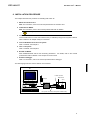
4. SYSTEM CONFIGURATION
The following figure shows the configuration of a system in which RTE-V831-TP is used.
Windows95, Windows NT
PC 9800 Series
PC interface card
PC 9800 Series PC
AC adapter (power)
GHS Multi
PC/AT
interface card
PARTNER/Win
PC/AT PC
Host system
interface cable
(supplied with the
interface card)
RTE-xxxx-TP
N-Wire cable
(for user system connection)
PC Card interface
Note-type PC
with a PC Card slot
ROM probe
(for user system connection)
GHS-multi,PARTNER/Win:
High-level language debuggers for RTE-V831-TP
PC:
PC capable of running Windows 95
PC 9800 Series PC interface card: Card supporting the PC 9800 C bus
PC/AT interface card:
Card supporting the PC/AT ISA bus
PC Card interface:
Type II card (version 2.1 of the PCMCIA specifications/
version 4.2 of the JEIDA specification or later)
Host system interface cable:
Cable for connecting RTE-V831-TP to the host card
AC adapter:
Dedicated power supply
RTE-xxxx-TP:
RTE-V831-TP
N-Wire cable:
Cable for connecting to the user system used for
debugging
ROM probe:
Probe for ROM emulation
5
RTE-V831-TP
Hardware User’s Manual
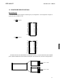
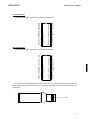
5. COMPONENT NAMES AND FUNCTIONS
This chapter shows the appearance of RTE-V831-TP, as well as the names and functions of its
components.
ROM USER POWER LED
N-Wire connector
ROM#1 connector
PC (host system) connector
3
1
5V
2
Power jack
4
ROM#2 connector
GN
D
EXT
POWER
HOS
T
Power LED
EXT connector
DCU USER POWER LED
Power jack
This is a connector for the power supply. Power is supplied by inserting the plug of the supplied
power supply into the jack.
Do not connect any device other than the supplied AC adapter
(RTE-PS01) to the power jack.
PC (host) connector (HOST)
This connector is used for connecting RTE-V831-TP to the PC (host system). The host system
interface cable is connected to this connector.
EXT connector (EXT)
This connector is used for external signal input and internal signal output.
N-Wire connector (N-Wire connector: JDCU1)
This connector is used for connecting RTE-V831-TP to the user system via N-Wire.
ROM emulator connector #1 (ROM#1 connector: JROM1)
This is connector No. 1 for connecting RTE-V831-TP to the user system to emulate ROMs.
ROM emulator connector #2 (ROM#2 connector: JROM2)
This is connector No. 2 for connecting RTE-V831-TP to the user system to emulate ROMs.
Power LED (POWER)
This LED lights steadily while the power to RTE-V831-TP is on.
DCU user system power LED (DCU USER POWER LED: DCU POWER)
This LED lights steadily while the power to the user system connected with the N-Wire connector is
on.
6
RTE-V831-TP
Hardware User’s Manual
ROM user system power LEDs (ROM USER POWER LEDs: ROM POWER 1/2/3/4)
These LEDs light steadily while the power to the power pins of the ROM sockets connected with the
ROM emulator connectors is on. The four LEDs have the following meanings:
If an 8-bit ROM probe is used:
LED1 to LED4 correspond to sockets ROM1 to ROM4 at the end of ROM probes, and light
steadily when the power to the power pins of the sockets is on.
If a 16-bit ROM probe is used:
LED1 and LED2 light steadily at the same time while:
The power to ROM socket #1 connected with connector ROM#1 is on.
LED3 and LED4 light steadily at the same time while:
The power to ROM socket #2 connected with connector ROM#2 is on.
7
RTE-V831-TP
Hardware User’s Manual
6. INSTALLATION PROCEDURE
This chapter describes the procedure for installing RTE-V831-TP.
1. Mount the interface card.
Note For information, refer to the manual provided with the interface card.
2. Install RTE for WIN32.
Note For information, refer to the manual provided with RTE for WIN32.
At this point, do not start CHKRTE32.EXE.
3. Connect RTE-V831-TP.
Connect RTE-V831-TP to the host interface card (or LAN-BOX) using the host system interface
cable. Make the AC adapter ready for connection.
4. Connect RTE-V831-TP to the user system.
Note For details, see Chapter 7.
5. Turn on the power.
Note For details, see Chapter 8.
6. Set RTE for WIN32.
Start CHKRTE32.EXE and set the necessary parameters. For details, refer to the manual
provided with RTE for WIN32 or see Chapter 9 of this manual.
7. Install the debugger.
Note For information, refer to the manual provided with the debugger.
The following figure shows how the devices are connected.
PC
N-Wire connector
ROM socket
AC adapter
V831
RTE-xxxx-TP
User system
User system connection cable (N-Wire & ROM cable)
8
RTE-V831-TP
Hardware User’s Manual
7. CONNECTION TO THE USER SYSTEM
The procedure for connecting RTE-V831-TP to the user system is described below.
Connection with the N-Wire cable
Connect the JDCU1 connector of RTE-V831-TP to the user system using the N-Wire cable supplied with
RTE-V831-TP.
Connection with a ROM probe
Connect the JROM1 or JROM2 connector of RTE-V831-TP to the ROM socket of the user system, using
a ROM probe of a type appropriate for the ROM of the user system. (ROM probes are options.)
Three types of ROM probe are available:
<DIP-32-ROM probe>
This probe allows emulation of up to four 8-bit ROMs.
On the RTE-V831-TP side, connect a probe labeled ROM1 and ROM2 to JROM1 and a probe
labeled ROM3 and ROM4 to JROM2.
On the user system side, connect ROM1, ROM2, ROM3, and ROM4 to the ROM sockets with the
lowest, second lowest, second highest, and highest addresses, respectively, if an 8-bit bus is used.
If a 16-bit bus is used, connect ROM1/ROM2 to the ROM sockets corresponding to D0-D7/D8-D15
of the lower addresses and ROM3/ROM4 to the ROM sockets corresponding to D0-D7/D8-15 of
the higher addresses.
<DIP-40-ROM and DIP-42-ROM probes>
These probes enable the emulation of up to two 16-bit ROMs.
On the RTE-V831-TP side, connect a probe labeled ROM1 to JROM1 and a probe labeled ROM2
to JROM2.
On the user system side, connect a probe labeled ROM1 to the ROM socket with the lower address
and a probe labeled ROM2 to the ROM socket with the higher address, if a 16-bit bus is used.
When connecting probes to ROM sockets, pay careful attention
to the ROM orientation. The dot mark indicates pin 1.
Note on the DIP-32-ROM probe
For 32-pin ROMs of 1MB or greater, there are two possible pin assignment schemes. Set the jumper on
the board for the ROM cable according to the ROM being used.
OE-:24-pin,A16:2-pin : 1-2 Jumpered
(factory setting)
OE-:2pin,A16:24-pin : 2-3 Jumpered
9
RTE-V831-TP
Hardware User’s Manual
8. POWERING ON AND OFF
The procedures for powering the system on and off are described below. Complete all the steps in the
installation procedure (such as cable connection) before powering the system on.
Powering on
1. Turn on the power to the host system.
2. Turn on the power to RTE-V831-TP. (Connect the dedicated AC adapter to the power jack of
RTE-V831-TP.)
3. Turn on the power to the user system.
4. Start the debugger.
Powering off
1. Quit the debugger.
2. Turn off the power to the user system.
3. Turn off the power to RTE-V831-TP. (Disconnect the AC adapter from RTE-V831-TP.)
4. Turn off the power to the host system.
Do not turn on the power to the user system before powering
on RTE-V831-TP. Doing so may cause a malfunction.
10
RTE-V831-TP
Hardware User’s Manual
9. RTE FOR WIN32
This chapter describes the setting of RTE for WIN32, with the focus on the aspects specific to RTEV831-TP.
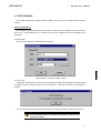
Starting ChkRTE32.exe
Start ChkRTE32.exe after RTE-V831-TP has been connected to the user system and the power to all the
devices is on. When RTE-V831-TP is installed for the first time, ChkRTE32.exe must be started once to
select RTE.
<Selecting RTE>
Set the Setup dialog box of ChkRTE32.exe, as follows.
*Select V831-TP or V832-TP in RTE: section .
<Function test>
If RTE-V831-TP is properly connected to the user system and capable of debugging, the following dialog
box appears upon the normal completion of the function test. In this state, control from the debugger is
possible.
If an error occurs during the test, the N-Wire cable is not properly connected. Check its connection.
Perform the ChkRTE32.exe function test after the RTE-V831-TP has
been connected to the user system and the power to all the devices
has been turned on.
11
RTE-V831-TP
Hardware User’s Manual
10. INITIALIZATION COMMANDS
Before debugging can be started, initialization is required. The following explains initialization using the
appropriate internal commands. If the debugger offers a means of initialization, they may be used instead.
(See Appendix A for an explanation of starting the internal commands and an explanation of the other
internal commands.)
env command
<Format>
env [[!]auto] [[!]reset] [[!]nmi] [[!]hldrq] [[!]int{00|01|02|03}] [[!]int{10|11|12|13}] [jtag{25|12}]
<Parameters>
[!]auto
If a break point is encountered during execution, the break point causes a temporary break.
Choose [Auto] to automatically perform the subsequent execution. Choose [!auto] to suppress it.
[!]reset
This parameter specifies whether the RESET pin is to be masked. Enter ! if it is not to be masked.
[!]nmi
This parameter specifies whether the NMI pin is to be masked. Enter ! if it is not to be masked.
[!]hldrq
This parameter specifies whether the HLDRQ pin is to be masked. Enter ! if it is not to be masked.
[!]int{00|01|02|03}
This parameter specifies that pins INT00 to INT03 are to be masked. Enter ! if they are not to be
masked.
[!]int{10|11|12|13}
This parameter specifies that pins int10 to int13 are to be masked. Enter ! if they are not to be
masked.
jtag[12|25]
This parameter specifies the JTAG clock for N-Wire. Usually, use jtag25.
<Function>
The env command sets the emulation environment. Enter only the parameters that need to be
changed. Parameters may be entered in any order. If the same parameter is entered twice, the last
entry of the parameter is valid. The initial values are as follows:
CPU Settings:
Auto Run
JTAGCLOCK
Signals Mask:
INT00
INT01
INT02
INT03
INT10
INT11
INT12
INT13
NMI
RESET
HLDRQ
= ON (auto)
= 25 MHz (jtag25)
= NO MASK (!int00)
= NO MASK (!int01)
= NO MASK (!int02)
= NO MASK (!int03)
= NO MASK (!int10)
= NO MASK (!int11)
= NO MASK (!int12)
= NO MASK (!int13)
= NO MASK (!nmi)
= NO MASK (!reset)
= NO MASK (!hldrq)
<Example>
env reset !nmi
RESET is masked while NMI is not.
12
RTE-V831-TP
Hardware User’s Manual
rom command
<Format>
rom [ADDRESS [LENGTH]] [512k|1m|2m|4m|8m|16m] [rom8|rom16] [bus8|bus16]
<Parameters>
ADDRESS [LENGTH]
ADDRESS:
Lowest address of the ROM to be emulated. (An error occurs if it does
not match a ROM boundary.)
LENGTH:
Number of bytes of the ROM to be emulated. (Must be specified in
boundary units of 16 bytes.)
512k|1m|2m|4m|8m|16m
Specify the bit size of the ROM to be emulated. Sizes from 512K bits to 16M bits can be
specified. For the 27C1028, for example, specify 1M bits.
rom8|rom16
Specify the number of data bits of the ROM to be emulated. Either 8 bits or 16 bits can
be specified. If a DIP-32-ROM probe is used, choose rom8; if a DIP-40/42-ROM probe
is used, choose rom16.
bus8|bus16|bus32
Specify the ROM bus size in the system to be emulated. 8 bits, 16 bits, or 32 bits can be
specified.
<Function>
The rom command sets the ROM emulation environment. Enter only the parameters that need to be
changed. Parameters may be entered in any order. If the same parameter is entered twice, only the
last entry is valid. The initial value of LENGTH is 0 (not used).
<Examples>
rom C0000 40000 1m rom16 bus16
The 256K bytes (40000) of the 27C1048 (16-bit ROM with a size of 1M bits), starting at
0xc0000, are emulated. Consequently, two 16-bit ROMs are emulated.
rom fff80000 80000 2m rom rom16 bus32
The 512K bytes (80000) of the 27c2048 (16-bit ROM with a size of 2M bits), starting at
0xfff80000, are emulated. Consequently, two 16-bit ROMs are emulated.
<Note>
Access to the range specified by the rom command results in direct access to internal emulation
memory. Access to addresses outside the range is performed via the processor bus.
13
RTE-V831-TP
Hardware User’s Manual
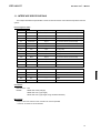
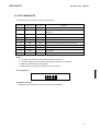
11. INTERFACE SPECIFICATIONS
This chapter describes the specifications of the connectors used for control that are required for the user
system.
Pin arrangement table
Pin number
Signal name
Input/output (user side)
Treatment (user side)
A1
TRCCLK
Output
33-Ω series resistor (recommended)
A2
TRCDATA0
Output
33-Ω series resistor (recommended)
A3
TRCDATA1
Output
33-Ω series resistor (recommended)
A4
TRCDATA2
Output
33-Ω series resistor (recommended)
A5
TRCDATA3
Output
33-Ω series resistor (recommended)
A6
TRCEND
Output
Open
A7
DDI
Input
10-kΩ pullup
A8
DCK
Input
10-kΩ pulldown
A9
DMS
Input
10-kΩ pulldown
A10
DDO
Output
A11
DRST-
Input
10-kΩ pulldown
A12
NC.
------
Open
A13
NC.
------
Open
Pin number
Signal name
Input/output (user side)
B1-B10
GND
------
Connection to the power GND
B11
NC.
------
Open
B12
NC.
------
Open
B13
+3.3V
------
Connection to the power
33-Ω series resistor (recommended)
Treatment (user side)
Connectors
Manufacturer: KEL
Models:
8830E-026-170S (straight)
8830E-026-170L (right angle)
8831E-026-170L (right angle, fixing hardware attached)
Wire length
Keep the wire from V831/2 to the connector as short as possible.
>>100 mm or shorter is recommended.
14
RTE-V831-TP
Hardware User’s Manual
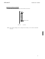
Layout of the connectors on the board
The figure below shows the physical layout of the connectors on the board.
B13 A13
B12 A12
Polarity indication
B2 A2
B1 A1
Board end
[Top View]
Note: When actually arranging the pins, design them according to the connector dimensional
information.
15
RTE-V831-TP
Hardware User’s Manual
12. EXT CONNECTOR
The specifications of the EXT connector are given below.
Pin number
Signal name
Input/output
1
Factory Use
Output
2
EXI0
Input
Description
Must be left unconnected.
External input signal #0 (pulled up with a 1-kΩ resistor). Edge
detectable.
3
Factory Use
Output
4
EXI1
Input
5
Factory Use
Output
6
EXI2
Input
7
Factory Use
Output
8
EXI3
Input
9
GND
--
10
TRG-
Output
Must be left unconnected.
External input signal #1 (pulled up with a 1-kΩ resistor)
Must be left unconnected.
External input signal #2 (pulled up with a 1-kΩ resistor)
Must be left unconnected.
External input signal #3 (pulled up with a 1-kΩ resistor)
Ground signal
Trigger output (goes low upon detection of a trace trigger)
Notes:
1. The inputs to EXI0, EXI1, EXI2, and EXI3 are at 5V-TTL level.
2. The TRG- signal is an open-collector signal (pulled up with a 1-kΩ resistor).
3. EXI0 can be specified as a trace trigger.
4. EXI0 to EXI3 are recorded in memory as trace information.
Pin arrangement:
9
7
5
3
1
10
8
6
4
2
JEXT pin arrangement
Applicable connector:
XG4M-1031 manufactured by Omron Corporation (or equivalent)
16
RTE-V831-TP
Hardware User’s Manual
13. ROM PROBE SPECIFICATIONS
DIP-32-ROM probe
The DIP-32-ROM probe supports the following two pin arrangements. The arrangement to support is
determined with the jumper on JP1.
JP1 1-2 jumpered
A19
A16
A15
A12
A7
A6
A5
A4
A3
A2
A1
A0
D0
D1
D2
GND
1
2
3
4
5
6
7
8
9
10
11
12
13
14
15
16
32
31
30
29
28
27
26
25
24
23
22
21
20
19
18
17
Vdd
A18
A17
A14
A13
A8
A9
A11
OEA10
CED7
D6
D5
D4
D3
A19
OEA15
A12
A7
A6
A5
A4
A3
A2
A1
A0
D0
D1
D2
GND
1
2
3
4
5
6
7
8
9
10
11
12
13
14
15
16
32
31
30
29
28
27
26
25
24
23
22
21
20
19
18
17
Vdd
A18
A17
A14
A13
A8
A9
A11
A16
A10
CED7
D6
D5
D4
D3
JP1 2-3 jumpered
The labels at the end are marked ROM1 and ROM2 at the factory. If you purchase another DIP-32-ROM
probe, replace the labels with those supplied to distinguish it from the first one, as shown in the figure below.
ROM1 -> ROM3
ROM2 -> ROM4
17
RTE-V831-TP
Hardware User’s Manual
DIP-40-ROM probe
The DIP-40-ROM probe supports the following pin arrangement.
(A18)
CSD15
D14
D13
D12
D11
D10
D9
D8
GND
D7
D6
D5
D4
D3
D2
D1
D0
OE-
1
2
3
4
5
6
7
8
9
10
11
12
13
14
15
16
17
18
19
20
40
39
38
37
36
35
34
33
32
31
30
29
28
27
26
25
24
23
22
21
Vdd
A17
A16
A15
A14
A13
A12
A11
A10
A9
GND
A8
A7
A6
A5
A4
A3
A2
A1
A0
DIP-42-ROM probe
The DIP-42-ROM probe supports the following pin arrangement.
A18
A17
A7
A6
A5
A4
A3
A2
A1
A0
CEGND
OED0
D8
D1
D9
D2
D10
D3
D11
1
2
3
4
5
6
7
8
9
10
11
12
13
14
15
16
17
18
19
20
21
42
41
40
39
38
37
36
35
34
33
32
31
30
29
28
27
26
25
24
23
22
A19
A8
A9
A10
A11
A12
A13
A14
A15
A16
BYTEGND
D15/A-1
D7
D14
D6
D13
D5
D12
D4
Vdd
The label at the end is labeled ROM1 or ROM2 at the factory. If you purchase another DIP-40-ROM or
DIP-42-ROM probe, replace the label with that supplied to distinguish it from the first one, as shown in the
figure below.
ROM1 -> ROM2
18
RTE-V831-TP
Hardware User’s Manual
14. PRECAUTIONS
This chapter provides precautionary information on the use of RTE-V831-TP.
Precautions related to operation
1) Do not turn on the power to the user system while the power to RTE-V831-TP is off. Doing so can
cause a malfunction.
2) RTE-V831-TP externally controls the debugging control circuit built into V831/2. Consequently,
RTE-V831-TP does not operate correctly unless the following conditions are satisfied:
* RTE-V831-TP is properly connected to the user system using the N-Wire cable.
* The power to the user system is on so that V831/2 can run correctly.
Precautions related to functions
1) The disassembly and display of real-time trace data is performed by reading the contents of memory
at the point the trace display command is issued, according to the branching information received
from V831/2. Consequently, the disassembly and display of the program located in RAM of the user
system is not correct if changes (including erroneous writing due to a runaway CPU) are made after
program execution. In addition, branching information may not be analyzed correctly because not
all branching information may be output.
19
RTE-V831-TP
Hardware User’s Manual
Revision History
Rev.1.0
December 9,1997
1st edition
Rev.2.0
Jun 15,1998
Added V832 information
RTE-V831-TP Hardware User's Manual
M781MNL02
Date of preparation: Jun 15, 1998 Rev2.0
20