1
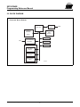
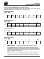
Programming User’s Manual
Remote Controller
SST65P542R
©2003 Silicon Storage Technology, Inc.
S74004-00-000
4/03
1
The SST logo and SuperFlash are registered trademarks of Silicon Storage Technology, Inc.
SoftPartition is a trademark of Silicon Storage Technology, Inc.
These specifications are subject to change without notice.
SST65P542R
Programming Reference Manual
TABLE OF CONTENTS
1.0 INTRODUCTION . . . . . . . . . . . . . . . . . . . . . . . . . . . . . . . . . . . . . . . . . . . . . . . . . . . . . . . . . . . . . . . . . . . . . . 4
2.0 BLOCK DIAGRAM . . . . . . . . . . . . . . . . . . . . . . . . . . . . . . . . . . . . . . . . . . . . . . . . . . . . . . . . . . . . . . . . . . . . . 5
3.0 PIN ASSIGNMENTS. . . . . . . . . . . . . . . . . . . . . . . . . . . . . . . . . . . . . . . . . . . . . . . . . . . . . . . . . . . . . . . . . . . . 6
4.0 MEMORY ORGANIZATION . . . . . . . . . . . . . . . . . . . . . . . . . . . . . . . . . . . . . . . . . . . . . . . . . . . . . . . . . . . . . . 7
5.0 MCU CORE AND INSTRUCTION SET . . . . . . . . . . . . . . . . . . . . . . . . . . . . . . . . . . . . . . . . . . . . . . . . . . . . . 8
5.1 Registers and Control Bit Assignments . . . . . . . . . . . . . . . . . . . . . . . . . . . . . . . . . . . . . . . . . . . . . . . . . . 8
5.1.1
5.1.2
5.1.3
5.1.4
5.1.5
Accumulator (A) . . . . . . . . . . . . . . . . . . . . . . . . . . . . . . . . . . . . . . . . . . . . . . . . . . . . . . . . . . . . . . . 9
Index Register (X) . . . . . . . . . . . . . . . . . . . . . . . . . . . . . . . . . . . . . . . . . . . . . . . . . . . . . . . . . . . . . 9
Program Counter (PC) . . . . . . . . . . . . . . . . . . . . . . . . . . . . . . . . . . . . . . . . . . . . . . . . . . . . . . . . . . 9
Stack Pointer (SP) . . . . . . . . . . . . . . . . . . . . . . . . . . . . . . . . . . . . . . . . . . . . . . . . . . . . . . . . . . . . . 9
Processor Status Word (PSW). . . . . . . . . . . . . . . . . . . . . . . . . . . . . . . . . . . . . . . . . . . . . . . . . . . 10
5.2 Addressing Modes . . . . . . . . . . . . . . . . . . . . . . . . . . . . . . . . . . . . . . . . . . . . . . . . . . . . . . . . . . . . . . . . . 10
5.2.1 Inherent (INH). . . . . . . . . . . . . . . . . . . . . . . . . . . . . . . . . . . . . . . . . . . . . . . . . . . . . . . . . . . . . . . .
5.2.2 Immediate (IMM) . . . . . . . . . . . . . . . . . . . . . . . . . . . . . . . . . . . . . . . . . . . . . . . . . . . . . . . . . . . . .
5.2.3 Direct (DIR) . . . . . . . . . . . . . . . . . . . . . . . . . . . . . . . . . . . . . . . . . . . . . . . . . . . . . . . . . . . . . . . . .
5.2.4 Extended (EXT) . . . . . . . . . . . . . . . . . . . . . . . . . . . . . . . . . . . . . . . . . . . . . . . . . . . . . . . . . . . . . .
5.2.5 Indexed, No Offset (IX). . . . . . . . . . . . . . . . . . . . . . . . . . . . . . . . . . . . . . . . . . . . . . . . . . . . . . . . .
5.2.6 Indexed, 8-bit Offset (IX1) . . . . . . . . . . . . . . . . . . . . . . . . . . . . . . . . . . . . . . . . . . . . . . . . . . . . . .
5.2.7 Indexed, 16-bit Offset (IX2) . . . . . . . . . . . . . . . . . . . . . . . . . . . . . . . . . . . . . . . . . . . . . . . . . . . . .
5.2.8 Relative (REL) . . . . . . . . . . . . . . . . . . . . . . . . . . . . . . . . . . . . . . . . . . . . . . . . . . . . . . . . . . . . . . .
5.2.9 Bit Set/Clear (BSC) . . . . . . . . . . . . . . . . . . . . . . . . . . . . . . . . . . . . . . . . . . . . . . . . . . . . . . . . . . .
5.2.10 Bit test and branch (BTB) . . . . . . . . . . . . . . . . . . . . . . . . . . . . . . . . . . . . . . . . . . . . . . . . . . . . . .
10
10
11
11
11
11
11
12
12
12
5.3 Instruction Set . . . . . . . . . . . . . . . . . . . . . . . . . . . . . . . . . . . . . . . . . . . . . . . . . . . . . . . . . . . . . . . . . . . . 13
6.0 I/O REGISTERS DEFINITION . . . . . . . . . . . . . . . . . . . . . . . . . . . . . . . . . . . . . . . . . . . . . . . . . . . . . . . . . . . 19
7.0 INTERRUPTS . . . . . . . . . . . . . . . . . . . . . . . . . . . . . . . . . . . . . . . . . . . . . . . . . . . . . . . . . . . . . . . . . . . . . . . . 22
8.0 RESETS AND CLOCKS . . . . . . . . . . . . . . . . . . . . . . . . . . . . . . . . . . . . . . . . . . . . . . . . . . . . . . . . . . . . . . . . 23
9.0 POWER-DOWN MODES . . . . . . . . . . . . . . . . . . . . . . . . . . . . . . . . . . . . . . . . . . . . . . . . . . . . . . . . . . . . . . . 24
9.1 STOP Mode . . . . . . . . . . . . . . . . . . . . . . . . . . . . . . . . . . . . . . . . . . . . . . . . . . . . . . . . . . . . . . . . . . . . . . 24
9.2 IDLE Mode . . . . . . . . . . . . . . . . . . . . . . . . . . . . . . . . . . . . . . . . . . . . . . . . . . . . . . . . . . . . . . . . . . . . . . . 24
©2003 Silicon Storage Technology, Inc.
S74004-00-000
2
4/03
SST65P542R
Programming Reference Manual
10.0 THE CORE TIMER . . . . . . . . . . . . . . . . . . . . . . . . . . . . . . . . . . . . . . . . . . . . . . . . . . . . . . . . . . . . . . . . . . . . 25
10.1 Computer Operating Properly Watchdog Timer Control Register (CWTC) . . . . . . . . . . . . . . . . . . . . . 26
10.2 Timer Control and Status Register (TCSR) . . . . . . . . . . . . . . . . . . . . . . . . . . . . . . . . . . . . . . . . . . . . . 26
10.2.1
10.2.2
10.2.3
10.2.4
10.2.5
10.2.6
10.2.7
Core Timer Overflow (CTOF) . . . . . . . . . . . . . . . . . . . . . . . . . . . . . . . . . . . . . . . . . . . . . . . . . . .
Real-Time Interrupt Flag (RTIF) . . . . . . . . . . . . . . . . . . . . . . . . . . . . . . . . . . . . . . . . . . . . . . . . .
Timer Overflow Enable (TOFE) . . . . . . . . . . . . . . . . . . . . . . . . . . . . . . . . . . . . . . . . . . . . . . . . .
Real-Time Interrupt Enable (RTIE). . . . . . . . . . . . . . . . . . . . . . . . . . . . . . . . . . . . . . . . . . . . . . .
Timer Overflow Flag Clear (TOFC) . . . . . . . . . . . . . . . . . . . . . . . . . . . . . . . . . . . . . . . . . . . . . .
Real-Time Interrupt Flag Clear (RTFC) . . . . . . . . . . . . . . . . . . . . . . . . . . . . . . . . . . . . . . . . . . .
Real-Time Interrupt Rate Select (RT1-RT0). . . . . . . . . . . . . . . . . . . . . . . . . . . . . . . . . . . . . . . .
26
26
26
26
26
26
27
10.3 Core Timer Counter Register (CTCR) . . . . . . . . . . . . . . . . . . . . . . . . . . . . . . . . . . . . . . . . . . . . . . . . . 27
10.4 COP Watchdog Timer (CWT) Reset . . . . . . . . . . . . . . . . . . . . . . . . . . . . . . . . . . . . . . . . . . . . . . . . . . 27
10.5 Timer During IDLE Mode . . . . . . . . . . . . . . . . . . . . . . . . . . . . . . . . . . . . . . . . . . . . . . . . . . . . . . . . . . . 27
11.0 CARRIER MODULATOR TRANSMITTER (CMT) . . . . . . . . . . . . . . . . . . . . . . . . . . . . . . . . . . . . . . . . . . . . 28
11.1 Carrier Generator . . . . . . . . . . . . . . . . . . . . . . . . . . . . . . . . . . . . . . . . . . . . . . . . . . . . . . . . . . . . . . . . . 28
11.1.1 Time Counter . . . . . . . . . . . . . . . . . . . . . . . . . . . . . . . . . . . . . . . . . . . . . . . . . . . . . . . . . . . . . . . 29
11.1.2 Carrier Generator Data Registers (CHR1, CLR1, CHR2, and CLR2) . . . . . . . . . . . . . . . . . . . . 30
11.2 Modulator . . . . . . . . . . . . . . . . . . . . . . . . . . . . . . . . . . . . . . . . . . . . . . . . . . . . . . . . . . . . . . . . . . . . . . . 31
11.2.1
11.2.2
11.2.3
11.2.4
11.2.5
Time mode . . . . . . . . . . . . . . . . . . . . . . . . . . . . . . . . . . . . . . . . . . . . . . . . . . . . . . . . . . . . . . . . .
FSK Mode . . . . . . . . . . . . . . . . . . . . . . . . . . . . . . . . . . . . . . . . . . . . . . . . . . . . . . . . . . . . . . . . .
Extended Space Operation . . . . . . . . . . . . . . . . . . . . . . . . . . . . . . . . . . . . . . . . . . . . . . . . . . . .
End Of Cycle (EOC) Interrupt. . . . . . . . . . . . . . . . . . . . . . . . . . . . . . . . . . . . . . . . . . . . . . . . . . .
Modulator Period Data Register (MDR1, MDR2, and MDR3) . . . . . . . . . . . . . . . . . . . . . . . . . .
31
32
33
33
35
12.0 PROGRAMMING FLOW DIAGRAM. . . . . . . . . . . . . . . . . . . . . . . . . . . . . . . . . . . . . . . . . . . . . . . . . . . . . . . 36
13.0 PACKAGING DIAGRAMS . . . . . . . . . . . . . . . . . . . . . . . . . . . . . . . . . . . . . . . . . . . . . . . . . . . . . . . . . . . . . . 39
©2003 Silicon Storage Technology, Inc.
S74004-00-000
3
4/03
SST65P542R
Programming Reference Manual
1.0 INTRODUCTION
The SST65P542R is a member of SST’s 8-bit, application-specific microcontroller family targeting IR remote controller applications.
The SST65P542R microcontroller provides high-functionality to infrared remote controller products. The device
offers flexibility to store different remote control configurations for controlling multiple appliances. The configurations are either programmed at the factory during the manufacturing process or updated through a web download
procedure using the serial interface.
Using the SuperFlash nonvolatile memory technology, the SST65P542R enhances the functionality of the conventional universal remote controller devices by integrating multiple functions of a remote controller system in a single
chip solution. The built-in LED I/O ports can directly drive LED indicators. The IR transmitter port drives signals to
the infrared transmitter, which, in turn, remotely controls appliances.
The SoftPartition flash memory architecture allows seamless partition of the program code, protocol tables, and
user data in the small granularity of 128 Byte sectors. The small sector size and fast Erase/Write time greatly
increase the time and power efficiency when altering the contents of the flash memory.
The embedded controller is designed and manufactured using SST’s patented and proprietary SuperFlash EEPROM
technology.
SST’s highly reliable SuperFlash technology provides significant advantages over conventional flash memory technology. These advantages translate into significant overall cost savings and reliability benefits for customers.
PRODUCT FEATURES
• 8-bit MCU Core
– Enhanced 6502 Microprocessor Megacell
• 4 MHz Typical Oscillator Clock Frequency
• 8 MHz maximum clock frequency
• 16 KByte of user programmable flash memory
• 352 Bytes SRAM
• IR Input Pin for Learning Mode
• Power-down Modes
• Carrier Modulator Transmitter
– Supports Baseband, Pulse Length Modulator (PLM), and Frequency Shift Keying (FSK)
• Core Timer / Counter
– 14-stage multifunctional ripple counter
– Includes timer overflow, POR, RTI, and CWT
• General Registers:
– Accumulator (8-bit)
– Index Register (8-bit)
• Control registers:
– Program Counter (16-bit)
– Stack Pointer (16-bit / 6 addressable bits)
– Condition code register (8-bit)
• Addressing modes supported:
1. Immediate 3. Extended
5. Indexed, no offset
7. Indexed, 16-bit offset 9. Bit test and branch
2. Direct
4. Relative
6. Indexed, 8-bit offset 8. Bit set/clear
10. Inherent
• Data types supported:
1. Bit data (manipulation instructions)
2. Byte data
©2003 Silicon Storage Technology, Inc.
S74004-00-000
4
4/03
SST65P542R
Programming Reference Manual
2.0 BLOCK DIAGRAM
FUNCTIONAL BLOCK DIAGRAM
Interrupt
Control
MCU Core
SuperFlash
EEPROM
IRQ#
RAM
352K x8
16K x8
Port A
IRO
Carrier Modulator
Transmitter
Port B
Port C
Timer/Counter Interrupt
Real-Time
Counter
Core Timer
/ Counter
COP Watchdog
Timer
4004 B2.5
©2003 Silicon Storage Technology, Inc.
S74004-00-000
5
4/03
SST65P542R
Programming Reference Manual
3.0 PIN ASSIGNMENTS
PB0
PB1
PB2
PB3
PB4
PB5
PB6
PB7
PA0
PA1
PA2
PA3
PA4
PA5
1
2
3
4
5
6
7
8
9
10
11
12
13
14
28-pin SOIC
28
27
26
25
24
23
22
21
20
19
18
17
16
15
OSC1
OSC2
VDD
IRQ#
RESET#
IRO
VSS
LPRST#
PC3
PC2
PC1
PC0
PA7
PA6
4004 F10.1
FIGURE
TABLE
3-1: PIN ASSIGNMENTS FOR 28-PIN SOIC
3-1: PIN DESCRIPTIONS
Symbol
Type1
16-9
PA[7:0]
I/O1
Port A: The state of any pin in Port A is software programmable and every line is configured as
an input during any external reset.
8-1
PB[7:0]
I/O with
internal
pull-ups
Port B: The state of any pin in Port B is software programmable and every line is configured as
an input during any external reset. Each I/O line contains a programmable interrupt/pull-up for
keyscan. PB[7] is used as a serial interface data line when the serial interface is enabled.
20-17
PC[3:0]
I/O
Port C: Every pin in Port C is a high-current pin and its state is software programmable. All lines
are configured as inputs during any external reset.
23
IRO
O
IRO: Suitable for driving IR LED biasing logic, the IRO pin is the high-current source and sink
output of the carrier modulator transmitter subsystem. Default state is low after any external
reset.
21
LPRST#
I
Low-Power Reset: An active-low pin, LPRST# function sets MCU to low-power reset mode.
The MCU, once in low-power reset mode, is held in reset with all processor clocks and crystal
oscillator halted. An internal Schmitt trigger is included in the LPRST# pin to improve noise
immunity.
24
RESET#
I
Reset: By setting the RESET# pin low the MCU is reset to a default state. An internal Schmitt
trigger is included in the RESET# pin to improve noise immunity.
28
OSC1
I
27
OSC2
O
Oscillator 1,2: These 2 pins interface with external oscillator circuits.
A crystal resonator, a ceramic resonator, or an external clock signal can be used.
25
IRQ#
I
Interrupt Request: The IRQ# is negative edge-sensitive triggered. An internal Schmitt trigger
is included in the IRQ# pin to improve noise immunity.
26
VDD
I
Power Supply: Supply Voltage
22
VSS
I
Ground: Circuit ground. (0V reference)
Pins
Name and Functions
T3-1.5 4004
1. I = Input
O = Output
©2003 Silicon Storage Technology, Inc.
S74004-00-000
6
4/03
SST65P542R
Programming Reference Manual
4.0 MEMORY ORGANIZATION
The SST65P542R has a total of 64 KByte of addressable memory. A memory map is shown in Figure 4-1. The
memory consists of 32 Bytes of I/O registers, 352 Bytes of SRAM, 16 KByte of user flash memory, and 128 Bytes
of user vectors.
0180H
I/O
Registers
Reserved
CWT
Reset
0000H
001FH
0020H
352 Bytes
SRAM
3FF0H
017FH
0180H
Reserved
BFFFH
BFFFH
C000H
User
Memory
Flash Memory
(128 sectors)
127 Sectors
(128 Bytes per sector)
16,256
Bytes
Flash Memory
FF80H
Read Protection
FF7FH
FF80H
Reserved
User
Vector
FFF4H
Reset and
Interrupt
Vectors
FFFFH
4004 F11.3
FFFFH
FIGURE
4-1: MEMORY MAP
©2003 Silicon Storage Technology, Inc.
S74004-00-000
7
4/03
SST65P542R
Programming Reference Manual
5.0 MCU CORE AND INSTRUCTION SET
This section provides a description of the MCU core registers, the instruction set and the addressing modes.
5.1 Registers and Control Bit Assignments
The MCU contains five registers, as shown in the programming model of Figure 5-1. The interrupt stacking order is
shown in Figure 5-2.
PROGRAM COUNTER
STACK POINTER
PCL
PCH
0 0 0 0 0 0 0 0
SP
1 1
ACCUMULATOR
INDEX REGISTER
PSW REGISTER
1
1
1
H
I
N
Z
C
Unused
Unused
Unused
Half Carry
Interrupt Disable
Negative
Zero
Carry
4004 F01.4
FIGURE
5-1: PROGRAMMING MODEL
©2003 Silicon Storage Technology, Inc.
S74004-00-000
8
4/03
SST65P542R
Programming Reference Manual
Unstacking increasing address
PSW
ACCUMULATOR (A)
INDEX REGISTER (X)
PCH
PCL
Stacking decreasing address
FIGURE
4004 F02.3
5-2: STACKING ORDER
Stacking decreases memory address and unstacking (Return) increases memory address.
5.1.1 Accumulator (A)
The accumulator is a general purpose 8-bit register used to hold operands and results of an arithmetic calculation
or data manipulations.
5.1.2 Index Register (X)
The index register is an 8-bit register, which can contain the indexed addressing value used to create an effective
address. The index register may also be used as a temporary storage area.
5.1.3 Program Counter (PC)
The program counter is a 16-bit register, which contains the address of the next byte to be fetched.
5.1.4 Stack Pointer (SP)
The stack pointer is a 16-bit register, which contains the address of the next free location on the stack. During an
MCU reset or the reset stack pointer (RSP) instruction, the stack pointer is set to location 00FFH. The stack pointer
is then decremented as data is pushed onto the stack and incremented as data is pulled from the stack. When
accessing memory, the 8 most significant bits are permanently set to 00H. These eight bits are appended to the
lower 8 significant register bits to produce an address within the range of 00C0H to 00FFH. Subroutines and interrupts may use up to 256 (decimal) locations. If 64 locations are exceeded, i.e. if stack pointer is pointing to 00C0H
and stacking operation carried out, the stack pointer wraps around to 00FFH and overwrites the previously stored
information. A subroutine call occupies two locations on the stack; an interrupt uses five locations.
©2003 Silicon Storage Technology, Inc.
S74004-00-000
9
4/03
SST65P542R
Programming Reference Manual
5.1.5 Processor Status Word (PSW)
The PSW is a 5-bit register. These bits can be individually tested by a program, and specific actions can be taken
as a result of their state. Each bit is explained in the following paragraphs.
5.1.5.1 Half Carry (H)
This bit is set during ADD and ADC operations to indicate that a carry has occurred between bits 3 and 4 of the
accumulator during an ADD or ADC operation.
5.1.5.2 Interrupt (I)
When this bit is set all maskable interrupts are masked. If an interrupt occurs while this bit is set, the interrupt is
latched and remains pending until the interrupt bit is cleared. After any reset, the interrupt mask is set and can be
cleared by software instruction (CLI).
5.1.5.3 Negative (N)
When set, this bit indicates that the result of the last arithmetic, logical, or data manipulation was negative.
5.1.5.4 Zero (Z)
When set, this bit indicates that the result of the last arithmetic, logical, or data manipulation was zero.
5.1.5.5 Carry/Borrow (C)
When set, this bit indicates that a carry or borrow out of the arithmetic logical unit (ALU) occurred during the last
arithmetic operation. This bit is also affected during bit test and branch instructions and during shifts and rotates.
5.2 Addressing Modes
Ten different addressing modes provide programmers with the flexibility to optimize their code for all situations. The
various indexed addressing modes make it possible to locate data tables, code conversion tables and scaling
tables anywhere in the memory space. Short indexed accesses are single byte instructions; the longest instructions (three bytes) enable access to tables throughout memory. Short absolute (direct) and long absolute
(extended) addressing are also included. One or two byte direct addressing instructions access all data bytes in
most applications.
Extended addressing permits jump instructions to reach all memory locations. The term ‘effective address’ (EA) is
used in describing the various addressing modes. The effective address is defined as the address from which the
argument for an instruction is fetched or stored. The ten addressing modes of the processor are described below.
Parentheses are used to indicate ‘contents of’ the location or register referred to. For example, (PC) indicates the
contents of the location pointed to by the PC (program counter). An arrow indicates ‘is replaced by’ and a colon
indicates concatenation of two bytes.
5.2.1 Inherent (INH)
In the inherent addressing mode, all the information necessary to execute the instruction is contained in the
opcode. Operations specifying only the index register or accumulator, as well as the control instruction, with no
other arguments are included in this mode. These instructions are one byte long.
5.2.2 Immediate (IMM)
In the immediate addressing mode, the operand is contained in the byte immediately following the opcode.
EA = PC+1; PC ←PC+2
©2003 Silicon Storage Technology, Inc.
S74004-00-000
10
4/03
SST65P542R
Programming Reference Manual
5.2.3 Direct (DIR)
In the direct addressing mode, the effective address of the argument is contained in a single byte following the
opcode byte. Direct addressing allows the user to directly address the lowest 256 bytes in memory with a single
two-byte instruction.
EA = (PC+1); PC ←PC+2
Address bus high byte ←0, Address bus low byte ←(PC+1)
5.2.4 Extended (EXT)
In the extended addressing mode, the effective address of the argument is contained in the two bytes following the
opcode byte. Instructions with extended addressing mode are capable of referencing arguments anywhere in memory with a single three-byte instruction.
EA = (PC+1):(PC+2); PC ←PC+3
Address bus high byte ←(PC+1); Address bus low byte ←(PC+2)
5.2.5 Indexed, No Offset (IX)
In the indexed, no offset addressing mode, the effective address of the argument is contained in the 8-bit index register. This addressing mode can access the first 256 memory locations. These instructions are only one byte long.
This mode is often used to move a pointer through a table or to hold the address of a frequently referenced RAM or
I/O location.
EA = (X); PC ←PC+1
Address bus high byte ←0; Address bus low byte ←(X)
5.2.6 Indexed, 8-bit Offset (IX1)
In the indexed, 8-bit offset addressing mode, the effective address is the sum of the contents of the unsigned 8-bit
index register and the unsigned byte following the opcode. Therefore the operand can be located anywhere within the
lowest 511 memory locations. This addressing mode is useful for selecting the mth element in an n element table.
EA = (X)+(PC+1); PC ←PC+2
Address bus high byte ←K; Address bus low byte ←(X)+(PC+1)
where K = the carry from the addition of (X) and (PC+1)
5.2.7 Indexed, 16-bit Offset (IX2)
In the indexed, 16-bit offset addressing mode, the effective address is the sum of the contents of the unsigned 8-bit
index register and the two unsigned bytes following the opcode. This address mode can be used in a manner similar to indexed, 8-bit offset except that this three-byte instruction allows tables to be anywhere in memory. As with
direct and extended addressing, the assembler determines the shortest form of indexed addressing.
EA = (X)+[(PC+1):(PC+2)]; PC ←PC+3
Address bus high byte ←(PC+1)+K; Address bus low byte ←(X)+(PC+2)
where K = the carry from the addition of (X) and (PC+2)
©2003 Silicon Storage Technology, Inc.
S74004-00-000
11
4/03
SST65P542R
Programming Reference Manual
5.2.8 Relative (REL)
The relative addressing mode is only used in branch instructions. In relative addressing, the contents of the 8-bit
signed byte (the offset) following the opcode is sign-extended and added to the PC if, and only if, the branch conditions are true. Otherwise, control proceeds to the next instruction. The span of relative addressing is from -126 to
+129 from the opcode address. The programmer need not calculate the offset when using the assembler, since it
calculates the proper offset and checks to see that it is within the span of the branch.
EA = PC+2+(PC+1); PC ←EA if branch taken;
otherwise PC ←PC+2
5.2.9 Bit Set/Clear (BSC)
In the bit set/clear addressing mode, the bit to be set or cleared is part of the opcode. The byte following the
opcode specifies the address of the byte in which the specified bit is to be set or cleared. Any read/write bit in the
first 256 locations of memory can be selectively set or cleared with a single two-byte instruction.
EA = (PC+1); PC ←PC+2
Address bus high byte ←0; Address bus low byte ←(PC+1)
5.2.10 Bit test and branch (BTB)
The bit test and branch addressing mode is a combination of direct addressing and relative addressing mode. The
bit to be tested and its condition (set or clear) is included in the opcode. The address of the byte to be tested is in
the single byte immediately following the opcode byte (EA1). The signed relative 8-bit offset in the third byte is signextended and added to the PC if the specified bit is set or cleared in the specified memory location. This single
three-byte instruction allows the program to branch based on the condition of any readable bit in the first 256 locations of memory. The span of branch is from -125 to +130 from the opcode address. The state of the tested bit is
also transferred to the carry bit of the condition code register.
EA1 = (PC+1); PC ←PC+2
Address bus high byte →0; Address bus low byte →(PC+1)
EA2 = PC+3+(PC+2); PC ←EA2 if branch taken;
otherwise PC ←PC+3
©2003 Silicon Storage Technology, Inc.
S74004-00-000
12
4/03
SST65P542R
Programming Reference Manual
5.3 Instruction Set
Table 5-1 summarizes the MCU instruction set. A description of the instructions and an explanation of abbreviations follows the table on page 18.
TABLE
5-1: MCU INSTRUCTION TABLE (1
OF
5)
Address
Mode (n)
Hex
Opcode
Number of
Machine Cycles
Number of
Bytes
Flags
Affected
Add memory to accumulator
with carry A+M+C →A
IMM
DIR
EXT
IX
IX1
IX2
A9
B9
C9
F9
E9
D9
2
3
4
3
4
5
2
2
3
1
2
3
H–NZC
ADD
Add memory to accumulator
A+M →A
IMM
DIR
EXT
IX
IX1
IX2
AB
BB
CB
FB
EB
DB
2
3
4
3
4
5
2
2
3
1
2
3
H–NZC
AND
“AND” memory with
accumulator
A&M →A
IMM
DIR
EXT
IX
IX1
IX2
A4
B4
C4
F4
E4
D4
2
3
4
3
4
5
2
2
3
1
2
3
––NZ–
ASR
Shift right one bit
(accumulator or memory)
b0 →C
b7 held constant
INH (A)
INH (X)
DIR
IX
IX1
47
57
37
77
67
3
3
5
5
6
1
1
2
1
2
––NZC
ASL
(same as LSL)
Shift left one bit
(accumulator or memory)
b7 →C
0 →b0
INH (A)
INH (X)
DIR
IX
IX1
48
58
38
78
68
3
3
5
5
6
1
1
2
1
2
––NZC
BCC
Branch on carry clear
Branch on C = 0
REL
24
3
2
–––––
BCLR
Clear bit n
BSC
11 + 2n
5
2
–––––
BCS
Branch on carry set
Branch on C = 1
REL
25
3
2
–––––
BEQ
Branch on result zero
Branch on Z = 1
REL
27
3
2
–––––
BHCC
Branch if half carry clear
Branch on H = 0
REL
28
3
2
–––––
BHCS
Branch if half carry set
Branch on H = 1
REL
29
3
2
–––––
BHI
Branch if higher
Branch if accumulator
is higher than memory
(unsigned)
REL
22
3
2
–––––
Mnemonic
Explanation
ADC
©2003 Silicon Storage Technology, Inc.
S74004-00-000
13
4/03
SST65P542R
Programming Reference Manual
TABLE
5-1: MCU INSTRUCTION TABLE (CONTINUED) (2 OF 5)
Address
Mode (n)
Hex
Opcode
Number of
Machine Cycles
Number of
Bytes
Flags
Affected
REL
24
3
2
–––––
Mnemonic
Explanation
BHS
Branch if higher or same
Branch if accumulator
is higher or same
as memory (C = 0)
BIH
Branch if interrupt line is high
REL
2F
3
2
–––––
BIL
Branch if interrupt line is low
REL
2E
3
2
–––––
BIT
Tests bits in memory: A^M
(logical compare)
IMM
DIR
EXT
IX
IX1
IX2
A5
B5
C5
F5
E5
D5
2
3
4
3
4
5
2
2
3
1
2
3
––NZ–
BLO
Branch if lower
Branch if accumulator is lower
Branch on
REL
25
3
2
–––––
BLS
Branch if low or same
Branch if accumulator is lower
than or equal
to memory
REL
23
3
2
–––––
BMC
Branch if interrupt
mask bit is clear
REL
2C
3
2
–––––
BMI
Branch if minus branch
on N = 1
REL
2B
3
2
–––––
BMS
Branch if interrupt
mask bit is set
Branch on I = 1
REL
2D
3
2
–––––
BNE
Branch if not equal
Branch on Z = 0
REL
26
3
2
–––––
BPL
Branch if plus
Branch on N = 0
REL
2A
3
2
–––––
BRA
Branch always
REL
20
3
2
–––––
BRN
Branch never
REL
21
3
2
–––––
BRCLR
Branch if bit n is clear
BTB
1 + 2n
5
3
––––C
BRSET
Branch if bit n is set
BTB
2n
5
3
––––C
BSET
Set bit n
BSC
10 + 2n
5
2
–––––
BSR
Branch to subroutine
REL
AD
6
2
–––––
CLC
Clear carry flag
0 →C
INH
98
2
1
––––0
CLI
Clear interrupt mask
bit 0 →I
INH
9A
2
1
–0–––
CLR
Clear
INH (A)
INH (X)
DIR
IX
IX1
4F
5F
3F
7F
6F
3
3
5
5
6
1
1
2
1
2
––01–
©2003 Silicon Storage Technology, Inc.
S74004-00-000
14
4/03
SST65P542R
Programming Reference Manual
TABLE
5-1: MCU INSTRUCTION TABLE (CONTINUED) (3 OF 5)
Address
Mode (n)
Hex
Opcode
Number of
Machine Cycles
Number of
Bytes
Flags
Affected
Arithmetic compare
memory and accumulator
(unsigned)
A-M
IMM
DIR
EXT
IX
IX1
IX2
A1
B1
C1
F1
E1
D1
2
3
4
3
4
5
2
2
3
1
2
3
––NZC
COM
Component
(one’s complement)
INH (A)
INH (X)
DIR
IX
IX1
43
53
33
73
63
3
3
5
5
6
1
1
2
1
2
––NZ1
CPX
Arithmetic compare
memory and index X
(unsigned)
X-M
IMM
DIR
EXT
IX
IX1
IX2
A3
B3
C3
F3
E3
D3
2
3
4
3
4
5
2
2
3
1
2
3
––NZC
DEC
Decrement by one
INH (A)
INH (X)
DIR
IX
IX1
4A
5A
3A
7A
6A
3
3
5
5
6
1
1
2
1
2
––NZ–
EOR
“Exclusive or” memory
with accumulator
A ^ M →A
IMM
DIR
EXT
IX
IX1
IX2
A8
B8
C8
F8
E8
D8
2
3
4
3
4
5
2
2
3
1
2
3
––NZ–
INC
Increment by one
INH (A)
INH (X)
DIR
IX
IX1
4C
5C
3C
7C
6C
3
3
5
5
6
1
1
2
1
2
––NZ–
JMP
Jump to new location
(PC + 1) →PCL
(PC + 2) →PCH
DIR
EXT
IX
IX1
IX2
BC
CC
FC
EC
DC
2
3
2
3
4
2
3
1
2
3
–––––
JSR
Jump to new location
saving return address
PC + 2↓
(PC + 1) →PCL
(PC + 2) →PCH
DIR
EXT
IX
IX1
IX2
BD
CD
FD
ED
DD
5
6
5
6
7
2
3
1
2
3
–––––
Mnemonic
Explanation
CMP
©2003 Silicon Storage Technology, Inc.
S74004-00-000
15
4/03
SST65P542R
Programming Reference Manual
TABLE
5-1: MCU INSTRUCTION TABLE (CONTINUED) (4 OF 5)
Address
Mode (n)
Hex
Opcode
Number of
Machine Cycles
Number of
Bytes
Flags
Affected
Load accumulator
with memory
M →A
IMM
DIR
EXT
IX
IX1
IX2
A6
B6
C6
F6
E6
D6
2
3
4
3
4
5
2
2
3
1
2
3
––NZ–
LDX
Load index X with memory
M →X
IMM
DIR
EXT
IX
IX1
IX2
AE
BE
CE
FE
EE
DE
2
3
4
3
4
5
2
2
3
1
2
3
––NZ–
LSL
(same as ASL)
Shift left one bit
(accumulator or memory)
b7 →C
0 →b0
INH (A)
INH (X)
DIR
IX
IX1
48
58
38
78
68
3
3
5
5
6
1
1
2
1
2
––NZC
LSR
Shift right one bit
(memory or accumulator)
b0 →C
0 →b7
INH (A)
INH (X)
DIR
IX
IX1
44
54
34
74
64
3
3
5
5
6
1
1
2
1
2
––0ZC
MUL
Multiplication
X * A →X: A
INH (A)
42
11
1
0–––0
NEG
Negate
(Two’s complement)
INH (A)
INH (X)
DIR
IX
IX1
40
50
30
70
60
3
3
5
5
6
1
1
2
1
2
––NZC
NOP
No operation
INH
9D
2
1
–––––
ORA
“OR” memory with
accumulator
A | M →A
IMM
DIR
EXT
IX
IX1
IX2
AA
BA
CA
FA
EA
DA
2
3
4
3
4
5
2
2
3
1
2
3
––NZ–
ROL
Rotate one bit left
through carry (memory
or accumulator)
INH (A)
INH (X)
DIR
IX
IX1
49
59
39
79
69
3
3
5
5
6
1
1
2
1
2
––NZC
ROR
Rotate one bit right
through carry (memory
or accumulator)
INH (A)
INH (X)
DIR
IX
IX1
46
56
36
76
66
3
3
5
5
6
1
1
2
1
2
––NZC
RSP
Reset stack pointer
INH
9C
2
1
–––––
RTI
Return from interrupt PC; P
INH
80
9
1
?????
Mnemonic
Explanation
LDA
©2003 Silicon Storage Technology, Inc.
S74004-00-000
16
4/03
SST65P542R
Programming Reference Manual
TABLE
5-1: MCU INSTRUCTION TABLE (CONTINUED) (5 OF 5)
Address
Mode (n)
Hex
Opcode
Number of
Machine Cycles
Number of
Bytes
Flags
Affected
Return from subroutine
PC ↑ ; PC + 1 →PC
INH
81
6
1
–––––
SBC
Subtract memory
from accumulator
with borrow
A-M-C →A
IMM
DIR
EXT
IX
IX1
IX2
A2
B2
C2
F2
E2
D2
2
3
4
3
4
5
2
2
3
1
2
3
––NZC
SEC
Set carry flag
1 →C
INH
99
2
1
––––1
SEI
Set interrupt mask bit
I →1
INH
9B
2
1
–1–––
STA
Store accumulator in memory
A →M
DIR
EXT
IX
IX1
IX2
B7
C7
F7
E7
D7
4
5
4
5
6
2
3
1
2
3
––NZ–
STX
Store index X in memory
X →M
DIR
EXT
IX
IX1
IX2
BF
CF
FF
EF
DF
4
5
4
5
6
2
3
1
2
3
––NZ–
SUB
Subtract memory
IMM
DIR
EXT
IX
IX1
IX2
A0
B0
C0
F0
E0
D0
2
3
4
3
4
5
2
2
3
1
2
3
––NZC
Mnemonic
Explanation
RTS
SWI
Software interrupt
INH
83
10
1
–1–––
TAX
Transfer accumulator
to index X
A →X
INH
97
2
1
–––––
TST
Test for negative or
zero
INH (A)
INH (X)
DIR
IX
IX1
4D
5D
3D
7D
6D
3
3
4
4
5
1
1
2
1
2
––NZ–
TXA
Transfer index X to
accumulator
X →A
INH
9F
2
1
–––––
T5-1.5
©2003 Silicon Storage Technology, Inc.
S74004-00-000
17
4004
4/03
SST65P542R
Programming Reference Manual
Description
The following is the description of each instruction and the operation during the execution of each instruction.
The key for MCU instructions is as follows:
The first three letters are the opcode the actual mnemonic of the instruction. The possible addressing modes are
indicated by the letters following the opcode and they are as follows:
IMM:
immediate addressing
INH (A):
inherent addressing with respect to Accumulator
INH (X):
inherent addressing with respect to Index Register
DIR:
direct addressing
EXT:
extended addressing
IX:
indexed addressing (no offset)
IX1:
indexed addressing with one byte offset
IX2:
indexed addressing with two byte offset
BSC:
bit set / clear
BTB:
bit test and branch
REL:
relative addressing
The following abbreviations are used besides the ones used for addressing mode:
A
accumulator
C
carry flag
H
half carry flag
I
interrupt flag
M
memory
N
negative flag
PC
program counter
PCL
program counter lower byte
PCH
program counter higher byte
SP
stack pointer
X
index register
Z
zero flag
|
OR function
&
AND function
^
Exclusive OR function
???
load PSW from stack
-
not affected
Machine cycle is two oscillator clock cycles.
©2003 Silicon Storage Technology, Inc.
S74004-00-000
18
4/03
SST65P542R
Programming Reference Manual
6.0 I/O REGISTERS DEFINITION
The 32 Bytes of I/O registers occupy address locations from 0000H to 001FH and include general purpose I/O pin
registers, on-chip peripheral control registers, and SuperFlash Function Registers.
TABLE
6-1: I/O REGISTER DESCRIPTIONS
Address
Location
Register Description
0000H
Port A Data Register
0001H
Port B Data Register
0002H
Port C Data Register
0003H
Reserved
0004H
Port A Data Direction Register
0005H
Port B Data Direction Register
0006H
Port C Data Direction Register
0007H
Reserved
0008H
Core Timer Control Status Register
0009H
Core Timer Counter Register
000AH
Port B Interrupt Control Register
000BH
SuperFlash Function Register (SFFR)
000CH
Port B Pull-up Control Register
000DH
COP Watchdog Timer Control Register (CWTC)
000EH
Serial Interface Control Register (SICON_TR)
000FH
Serial Interface Control Register (SICON_LSBF)
0010H
Carrier Generator High Data Register1 (CHR1)
0011H
Carrier Generator Low Data Register1 (CLR1)
0012H
Carrier Generator High Data Register2 (CHR2)
0013H
Carrier Generator Low Data Register2 (CLR2)
0014H
Modulator Control and Status Register (MCSR)
0015H
Modulator Data Register1 (MDR1)
0016H
Modulator Data Register2 (MDR2)
0017H
Modulator Data Register3 (MDR3)
0018H
Power Save Control Register (PSCR)
0019H
Serial Interface Control Register (SICON_SI)
001AH
Serial Interface Data Register (SIDAT)
001BH
Serial Interface Status Register (SISTA)
001CH
Serial Interface Baud-Rate Register (SIBDR)
001DH
Serial Interface Control Register (SICON_AP)
001EH
Serial Interface Control Register (SICON_ENSI)
001FH
IR Input Control Register
T6-1.3
©2003 Silicon Storage Technology, Inc.
4004
S74004-00-000
19
4/03
SST65P542R
Programming Reference Manual
TABLE
6-2: BIT DEFINITIONS
OF
I/O REGISTERS (1
OF
2)
Addr
Register Name
Bit7
Bit6
Bit5
Bit4
Bit3
Bit2
Bit1
Bit0
0000H
Port A Data Register
PA7
PA6
PA5
PA4
PA3
PA2
PA1
PA0
0001H
Port B Data Register
PB7
PB6
PB5
PB4
PB3
PB2
PB1
PB0
0002H
Port C Data Register
X
X
X
X
PC3
PC2
PC1
PC0
0003H
Reserved
X
X
X
X
X
X
X
X
0004H
Port A Data
Direction Register
DDRA7
DDRA6
DDRA5
DDRA4
DDRA3
DDRA2
DDRA1
DDRA0
0005H
Port B Data
Direction Register
DDRB7
DDRB6
DDRB5
DDRB4
DDRB3
DDRB2
DDRB1
DDRB0
0006H
Port C Data
Direction Register
X
X
X
X
DDRC3
DDRC2
DDRC1
DDRC0
0007H
Reserved
0008H
Core Timer Control Status Register
X
X
X
X
X
X
X
X
CTOF
RTIF
TOFE
RTIE
TOFC
TRFC
RT1
RT0
0009H
Core Timer Counter
Register
X
X
X
X
X
X
X
X
000AH
Port B Interrupt
Control Register
INPRB7
INPRB6
INPRB5
INPRB4
INPRB3
INPRB2
INPRB1
INPRB0
000BH
SuperFlash
Function Register
PREN
MEREN
SEREN
X
PROG
MERA
SERA
X
000CH
Port B Pull-up
Control Register
X
X
X
X
X
X
PU1
PU0
000DH
CWT Control Register
X
X
X
X
X
X
X
CWT_EN
000EH
Serial Interface
Control Register
X
X
X
X
X
X
TR
X
000FH
Serial Interface
Control Register
X
X
X
X
X
LSBF
X
X
0010H
Carrier Generator High
Data Register (CHR1)
IROLN
CMTPOL
PH5
PH4
PH3
PH2
PH1
PH0
0011H
Carrier Generator Low
Data Register (CLR1)
IROLP
X
PL5
PL4
PL3
PL2
PL1
PL0
0012H
Carrier Generator High
Data Register 2(CHR2)
X
X
SH5
SH4
SH3
SH2
SH1
SH0
0013H
Carrier Generator Low
Data Register 2(CLR2)
X
X
SL5
SL4
SL3
SL2
SL1
SL0
0014H
Modulator Control and
Status Register (MCSR)
EOC
DIV2
EIMSK
EXSPC
BASE
MODE
EOCIE
MCGEN
0015H
Modulator Data
Register 1(MDR1)
MB11
MB10
MB9
MB8
SB11
SB10
SB9
SB8
0016H
Modulator Data
Register 2(MDR2)
MB7
MB6
MB5
MB4
MB3
MB2
MB1
MB0
0017H
Modulator Data
Register 3(MDR3)
SB7
SB6
SB5
SB4
SB3
SB2
SB1
SB0
0018H
Power Saving
Control Register (PSCR)
EN
X
X
X
X
X
STOP
IDL
0019H
Serial Interface
Control Register
X
X
X
X
X
X
X
SI
X = Reserved (Recommended to write “0” to reserved bits for future compatibility)
©2003 Silicon Storage Technology, Inc.
T6-2.5
S74004-00-000
20
4004
4/03
SST65P542R
Programming Reference Manual
TABLE
6-2: BIT DEFINITIONS
OF
I/O REGISTERS (CONTINUED) (2
OF
2)
Addr
Register Name
Bit7
Bit6
Bit5
Bit4
Bit3
Bit2
Bit1
Bit0
001AH
Serial Interface
Data Register
D7
D6
D5
D4
D3
D2
D1
D0
001BH
Serial Interface
Status Register
X
X
S5
S4
S3
X
X
X
001CH
Serial Interface
Baud-Rate Register
X
X
X
X
F3
F2
F1
F0
001DH
Serial Interface
Control Register
X
X
X
X
AP
X
X
X
001EH
Serial Interface
Control register
X
X
X
ENSI
X
X
X
X
001FH
IR Input Control
Register
X
X
X
X
X
X
IREN
IRIN
X = Reserved (Recommended to write “0” to reserved bits for future compatibility)
T6-2.5
4004
Please see Section 10.0 for Core Timer and Section 11.0 for CMT register definitions. All other register definitions
are described in detail in the SST65P542R data sheet.
©2003 Silicon Storage Technology, Inc.
S74004-00-000
21
4/03
SST65P542R
Programming Reference Manual
7.0 INTERRUPTS
The MCU has 6 sources of interrupts including reset, a software interrupt and 4 hardware interrupt lines. If more
than one interrupt line is active, the one with highest priority will be serviced first. The interrupt priority from high to
low is hardware reset, software interrupt, external interrupt, CMT interrupt, Core Timer interrupt, and Serial Interface interrupt. See Table 7-1 for Interrupt Address Vectors.
TABLE
7-1: MCU INTERRUPT ADDRESS VECTORS
Description
Interrupt
Address
Reset
FFFEH-FFFFH
SWI
FFFCH-FFFDH
Software interrupt vector FFFCH higher byte, FFFDH lower byte
External/Port B
FFFAH-FFFBH
External/Port B interrupt vector FFFAH higher byte, FFFBH lower byte
Restart vector FFFEH higher byte, FFFFH lower byte
CMT
FFF8H-FFF9H
CMT interrupt vector FFF8H higher byte, FFF9H lower byte
Core Timer
FFF6H-FFF7H
Core Timer interrupt vector FFF6H higher byte, FFF7H lower byte
Serial Interface
FFF4H-FFF5H
Serial Interface interrupt vector FFF4H higher byte, FFF5H lower byte
T7-1.3
4004
All four interrupt lines are masked by the interrupt mask bit (I bit of the Process Status Word Register). The software interrupt is generated by SWI instruction similar to that of any hardware instruction except that it is not
maskable (the execution of the SWI instruction is independent of the state of the mask bit).
All external interrupt lines are falling edge triggered and interrupts are always checked before fetching the next
instruction.
If interrupt is recognized, before the Program counter jumps to one of the address vectors, the Program Counter,
Index Register, Accumulator, and the Process Status Word Register are pushed on to the stack (see Figure 5-2).
©2003 Silicon Storage Technology, Inc.
S74004-00-000
22
4/03
SST65P542R
Programming Reference Manual
8.0 RESETS AND CLOCKS
SST65P542R has two sources for external reset: LPRST# and RESET#.
After LPRSET# switches from low to high, 4064 clock cycles are counted before the reset vector address appears
on the internal address bus. RESET# immediately resets the MCU without counting the 4064 clock cycles.
Crystal oscillator clock is divided by two to arrive at internal processor and peripheral clock. Figure 8-1 shows
RESET# and LPRST# timing diagram.
LPRST#4
OSC12
4064tCYC
tCYC
INTERNAL
PROCESSOR
CLOCK1
INTERNAL
ADDRESS
BUS1
FFFE
INTERNAL
DATA
BUS1
NEW
PCH
FFFF
NEW
PCL
NEW PC
NEW PC
FFFE
OP
CODE
FFFE
FFFE
FFFE
3FFF
PCH
PCL
NEW PC
NEW PC
OP
CODE
tRL3
RESET#
4004 F18.2
Notes:
1. Internal timing signal and bus information are not available externally.
Internal Processor Clock is half the frequency of OSC1.
2. OSC1 line is not meant to represent frequency. It is only used to represent time.
3. The next rising edge of the internal processor clock following the rising edge of RESET#
initiates the reset sequence. tRL is 1.5tCYC minimum.
4. The LPRST# pin resets the CPU like RESET#. However, 4064 clock cycles are
counted before the reset vector address appears on the internal address bus.
FIGURE
8-1: RESET#
AND
LPRST# TIMING DIAGRAM
©2003 Silicon Storage Technology, Inc.
S74004-00-000
23
4/03
SST65P542R
Programming Reference Manual
9.0 POWER-DOWN MODES
SST65P542R offers two modes to reduce system power consumption.
9.1 STOP Mode
To enter the STOP Mode, write 01H to the Power Saving Control Register (PSCR - 0018H). Upon completion of the
Write operation to the PSCR, the internal oscillator is turned off, halting all internal processing, including CMT and
timer operations.
The microcontroller can be brought out of the STOP Mode by external/Port B interrupts, LPRST# or RESET#.
When external interrupt is asserted (either on IRQ# or Port B pins (when Port B interrupt is enabled)), interrupt will
be serviced if mask bit (I bit) is clear, otherwise interrupt will not be serviced. MCU will resume operation to the next
instruction byte following the STOP mode enabling Write operation.
The STOP bit will be set to 1 when the device has ben brought out of STOP mode. The I bit will not be affected.
9.2 IDLE Mode
To enter IDLE Mode, write 02H to Power Saving Control Register (0018H). The IDLE Mode consumes more power
than the STOP Mode. Upon completion of the Write operation to the PSCR, all modules remain active except MCU
clock processing is suspended. Any interrupt or reset will cause the MCU to exit IDLE mode.
When an interrupt is asserted, interrupt will be serviced if mask bit (I bit) is clear, otherwise interrupt will not be serviced. MCU will resume operation to the next instruction byte following the IDLE mode enabling Write operation.
The IDLE bit will be set to 1 when the device has been brought out of IDLE mode. The I bit will not be affected.
©2003 Silicon Storage Technology, Inc.
S74004-00-000
24
4/03
SST65P542R
Programming Reference Manual
10.0 THE CORE TIMER
The core timer is a 14-stage, multifunctional ripple counter. Its features include Timer Overflow (TO), Power-On
Reset (POR), Real-Time Interrupt (RTI), and COP Watchdog Timer (CWT).
The core timer operates as follows:
1. The internal peripheral clock is divided by four, driving an 8-bit ripple counter. At any time, the counter value
can be read by accessing the Timer Counter Register (TCR) address 0009H.
2. At the last stage of the counter, a timer overflow is implemented. This gives a possible interrupt rate of the
internal peripheral clock, E/1024.
3. After three more stages, the clock, RTIOUT, now E/4096, drives the real-time interrupt circuit (RTI).
4. The RTI circuit has three divider stages with a 4:1 selector.
5. The output of the RTI circuit is divided by eight. This drives the CWT circuit.
6. The Timer Control and Status register at location 0008H contains the RTI rate selector bits and the RTI and
CTOF enable bits and flags.
Internal Bus
8
Internal Peripheral Clock (E)1
8
COP
Clear
E÷4
Timer Counter Register (TCR)
0009h
E ÷ 210
÷4
E ÷ 212
POR
5-Bit Counter
C ÷ 215 C ÷ 214 C ÷ 213 C ÷ 212
RTI Select Circuit 1
Overflow
Detect
Circuit
TCSR
CTOF
RTIF
RTIOUT
TOFE
RTIE
TOFC
RTFC
0008h
RT1
RT0
Timer Control &
Status Register
COP Watchdog
Timer (÷8)
Interrupt Circuit
To Reset
Logic
To Interrupt
Logic
4004 F12.5
Note:
1. Internal Peripheral Clock is oscillator clock divided by two.
FIGURE 10-1: CORE TIMER BLOCK DIAGRAM
©2003 Silicon Storage Technology, Inc.
S74004-00-000
25
4/03
SST65P542R
Programming Reference Manual
10.1 Computer Operating Properly Watchdog Timer Control Register (CWTC)
Writing to CWT Control register (000DH) can enable/disable core timer.
CWT Control Register
Address:
Bit 7
R
Default
000DH
6
X
5
X
4
X
3
X
2
X
1
X
Bit 0
CWT_EN
1
CWT_EN: ‘1’ CWT disabled;‘0’ CWT enabled
10.2 Timer Control and Status Register (TCSR)
The TCSR includes the timer interrupt flag, the timer interrupt enable bits, and the real-time interrupt rate select
bits. The table below shows the default value of each bit in the TCSR immediately after reset.
Timer Control and Status Register
Address:
Read:
Write:
Reset
0008H
Bit 7
CTOF
X
0
6
RTIF
X
0
5
4
TOFE
RTIE
0
0
3
0
TOFC
0
2
0
RTFC
0
1
Bit 0
RT1
RT0
1
1
10.2.1 Core Timer Overflow (CTOF)
CTOF is a read-only status bit set when the 8-bit ripple counter rolls over from FFH to 00H. Writing a logical “1” to
TOFC bit clears the CTOF. Writing to CTOF has no affect. Reset clears CTOF.
10.2.2 Real-Time Interrupt Flag (RTIF)
The Real Time Interrupt circuit contains a 3-stage divider and a one-of-four choice selector. The input frequency to
the RTI is (E/4096) and after three other divider stages allows a maximum interrupt period of 16 milliseconds at an
internal peripheral clock rate of 2.048MHz. RTIF is a read-only status bit which is set when the output of the
selected (one-of-four) divider stage goes active. Clearing the RTIF is done by writing a logical “1” to RTFC. Writing
to RTIF has no affect. Reset clears the RTIF bit.
10.2.3 Timer Overflow Enable (TOFE)
When the TOFE bit is set, a MCU interrupt request is generated only if CTOF bit is set. Reset clears this bit.
10.2.4 Real-Time Interrupt Enable (RTIE)
When the RTIE bit is a set, a MCU interrupt request is generated only if RTIF bit is set. Reset clears this bit.
10.2.5 Timer Overflow Flag Clear (TOFC)
CTOF is cleared when logical “1” is written to TOFC. Writing a “0” to TOFC has no effect on CTOF. TOFC has a “0”
as default.
10.2.6 Real-Time Interrupt Flag Clear (RTFC)
RTIF is cleared when RTFC bit is written to as “1”. Writing a “0” to RTFC has no effect on RTIF. RTFC has “0” as
default.
©2003 Silicon Storage Technology, Inc.
S74004-00-000
26
4/03
SST65P542R
Programming Reference Manual
10.2.7 Real-Time Interrupt Rate Select (RT1-RT0)
These two bits select any one-of-four taps from the real-time interrupt circuit stages. Please reference Table 10-1.
Reset sets these two bits to 11, selecting the lowest periodic rate, and gives the maximum time to alter these bits if
necessary. CWT should be cleared before changing RTI taps. If the selected tap is modified during a cycle in which
the counter is switching, a RTIF could be missed or an additional RTIF could be generated.
TABLE 10-1: RTI
AND
CWT RATES
RTI Rate
E = 2.048-MHz
AT
4.096 MHZ OSCILLATOR
Minimum CWT Rates
E = 2.048-MHz
RT1-RT0
2 ms
212 ÷ E
4 ms
213
8 ms
16 ms
215
Maximum CWT Rates
E = 2.048-MHz
00
(215-212)/E
14 ms
(215)/E
16 ms
÷E
01
(216-213)/E
28 ms
(216)/E
32 ms
214 ÷ E
10
(217-214)/E
56 ms
(217)/E
64 ms
11
(218-215)/E
112 ms
(218)/E
128 ms
÷E
T10-1.2
4004
10.3 Core Timer Counter Register (CTCR)
The TCR is a read-only register that contains the current value of the 8-bit ripple counter. This counter is clocked by
divided-by-four peripheral clock (E/4) and can be used for various timing related functions, including a softwareinput capture. Extended time periods can be achieved using the Timer Overflow function to increment a temporary
RAM storage location, there by simulating a 16-bit or larger counter.
Core Timer Counter Register (CTCR)
Address:
0009H
Bit 7
6
5
4
3
2
1
Bit 0
Read:
D7
D6
D5
D4
D3
D2
D1
D0
Write:
X
X
X
X
X
X
X
X
Reset
0
0
0
0
0
0
1
1
10.4 COP Watchdog Timer (CWT) Reset
The CWT objective is to prevent the device to become stuck or locked-up.
The COP Watchdog Timer (CWT) function is achieved by using the output of the RTI circuit and further dividing by
8. The minimum reset rates are listed in Table 10-1.
If the CWT circuit times out, an internal reset is generated. This internal reset is equivalent to RESET# pin reset.
To clear the CWT, write 00H to address 3FF0H. When CWT is cleared, only the final divide-by-eight output of the
RTI is cleared.
10.5 Timer During IDLE Mode
The MCU clock is stopped during IDLE mode, but the timer remains active. If interrupts are enabled, a timer interrupt will cause the processor to exit IDLE mode.
©2003 Silicon Storage Technology, Inc.
S74004-00-000
27
4/03
SST65P542R
Programming Reference Manual
11.0 CARRIER MODULATOR TRANSMITTER (CMT)
The carrier modulator transmitter (CMT) module is tailored for the IR remote controller applications. This module is
built by hardware with programmable ability for a wide variety of encoding schemes. The incorporated hardware
can off-load MCU to perform lengthy time-consuming tasks associated with code generation. It’s designed to handle most of the protocols. When a special protocol is needed, the CMT modulator can be disabled. A CMT register
can be used to change the state of the infrared out pin (IRO) directly.
The CMT module consists of three blocks: carrier generator, modulator, and transmitter output. The block diagram
is shown in Figure 11-1.
Carrier
Output
fosc
Modulator
Output
Primary/
Secondary
Select
Carrier
Generator
Mode
Polarity
Transmitter
IRO
Pin
Modulator
Base
Divide-by-two
4004 F20.0
FIGURE 11-1: CARRIER MODULATOR TRANSMITTER MODULE BLOCK DIAGRAM
11.1 Carrier Generator
The carrier generator has a resolution of 500ns time steps with a 2MHz fosc. The high and low times of the carrier
signal can be programmed by user independently to determine both period and duty cycle of carrier signal. The
period of carrier signal can be from 1 us (1MHz) to 64 us (15.6KHz) in 500ns increments. The duty cycle resolution
is depend on the number of counts required to complete the carrier period. These counts are split between high
and low times of the carrier signal. The longer the carrier signal period (the lower carrier signal frequency) the
higher the resolution (as a percentage of the total period) of carrier signal duty cycle.
In carrier generator block, there are two sets of high and low times, i.e., two set of carrier signal period (frequency)
can be selected. In normal mode (subsequently referred to as time mode), just one set will be used. In FSK (frequency shift key) mode, the modulator selects the two sets of carrier frequency base on the data to be modulated
to generate dual frequency FSK protocols without MCU intervention. When the BASE bit in the modulator control
and status register (MCSR) is set, the carrier output to the modulator is held high continuously to allow for the generation of baseband protocols.
©2003 Silicon Storage Technology, Inc.
S74004-00-000
28
4/03
SST65P542R
Programming Reference Manual
To enable carrier generator clocks, the MCGEN bit in the MCSR must be set and the BASE bit in the MCSR must
be cleared. The block diagram is shown below:
Primary High Count Register
High Time Counter
Secondary High Count Register
Carrier
Output
Primary/Secondary Select
Primary Low Count Register
Low Time Counter
Secondary Low Count Register
4004 F21.0
FIGURE 11-2: CARRIER GENERATOR BLOCK DIAGRAM
11.1.1 Time Counter
The high or low time counter is a 6-bit up counter. Only one counter is counting at a certain time. After each increment, the contents of the counter are compared with the appropriate high or low count value register. When the
value is reached, the counter is reset and stopped. Meanwhile the other counter is enabled for counting. Assuming
that the high time counter is currently active. The carrier output will be high and remand high until it reaches the
high time register value. Then, the carrier will be driven low and the low time counter is activated. The carrier output
will be low and remand low until it reaches the low time register value. Then, the carrier will be driven high and the
high time counter is activated. The cycle repeats automatically generating a periodic carrier signal that is feed into
the modulator block. The lowest frequency (maximum period) and highest frequency (minimum period) which can
be generated are defined as:
fmax = fosc ÷ (2×1) Hz
fmin = fosc ÷ (2×(26 -1)) Hz
In the general case, the carrier generator output frequency is:
fout = fosc ÷ (Highcount + Lowcount) Hz
where: 0< Highcount < 64 and 0< Lowcount < 64
The duty cycle of the carrier signal is:
Highcount
Duty cycle = ----------------------------------------------------------Highcount + Lowcount
©2003 Silicon Storage Technology, Inc.
S74004-00-000
29
4/03
SST65P542R
Programming Reference Manual
11.1.2 Carrier Generator Data Registers (CHR1, CLR1, CHR2, and CLR2)
There are two sets of Carrier Generator Data Registers: Primary and secondary. Each set contains one high time
register (CHR1, CHR2) and one low time register (CLR1, CLR2) as shown below.
Carrier Data Register (CHR1)
Address:
Read:
Write:
Reset
0010H
Bit 7
6
5
4
3
2
1
Bit 0
IROLN
CMTPOL
PH5
PH4
PH3
PH2
PH1
PH0
0
0
U
U
U
U
U
U
U = Unaffected
Carrier Data Register (CLR1)
Address:
Read:
Write:
Reset
0011H
Bit 7
6
5
4
3
2
1
Bit 0
IROLP
0
PL5
PL4
PL3
PL2
PL1
PL0
0
0
U
U
U
U
U
U
U = Unaffected
Carrier Data Register (CHR2)
Address:
Read:
Write:
Reset
0012H
Bit 7
6
5
4
3
2
1
Bit 0
0
0
SH5
SH4
SH3
SH2
SH1
SH0
0
0
U
U
U
U
U
U
U = Unaffected
Carrier Data Register (CHR2)
Address:
Read:
Write:
Reset
0013H
Bit 7
6
5
4
3
2
1
Bit 0
0
0
SL5
SL4
SL3
SL2
SL1
SL0
0
0
U
U
U
U
U
U
U = Unaffected
PH0-PH5 and PL0-PL5
Primary Carrier High (PH0-PH5) and Low (PL0-PL5) Time value
These bits contain the number of input clocks for the carrier high and low time periods. When operating
in timer mode, this register pair is always selected. When operating in FSK mode, the modulator
alternately selects this register pair and the secondary register pair. The primary carrier high and low
time values are undefined out of reset. These bits must be written to nonzero values before the carrier
generator is enabled to avoid spurious results.
SH0-SH5 and SL0-SL5
Secondary Carrier High (SH0-SH5) and Low (SL0-SL5) Time Value
These bits contain the number of input clocks for the carrier high and low time periods. When operating
in time mode, this register pair is never selected. When operating in FSK mode, the modulator
alternately selects this register pair and the primary register pair. The secondary carrier high and low
©2003 Silicon Storage Technology, Inc.
S74004-00-000
30
4/03
SST65P542R
Programming Reference Manual
time values are undefined out of reset. These bits must be written to nonzero values before the carrier
generator is enabled to avoid spurious results.
CMTPOL
CMT Output Polarity
This bit controls the polarity of the CMT output (IRO). When this bit is set to zero, the CMT output is
active high. When this bit is set to one, the CMT output is active low. The reset state of this bit is zero.
IROLN and IROLP
IRO Latch Control
The IRO latch state can be read from either IROLN or IROLP bits. The IRO latch state can be updated
with being written on either negative or positive edge of the internal processor clock (fosc/2). By writing
to IROLN updates the IRO latch on the negative edge. By writing to IROLP updates the IRO latch on
the positive edge. The IRO latch is cleared out of reset.
11.2 Modulator
The modulator can operate in two modes (Time and FSK) with a resolution of 4 us (2MHz external oscillator). It can
count either system clocks to provide real-time control or it can count carrier clocks for self-clocked protocols. In
time mode, the modulator counts clocks derived from the system oscillator and modulates a single-carrier frequency (TIME) or no carrier (baseband). In FSK mode, the modulator counts carrier periods and providing a signal
to switch the carrier generator between high/low time register buffers to alternate between two carrier frequencies
whenever a modulation period (mark+space counts) expires.
When the modulator is enabled (MCGEN=1), the space period register (SREG) is loaded with the contents of its
buffer (SBUFF), the mark buffer register (MBUFF) is loaded into a 12-bit down counter, and the modulator gate is
opened for carry signal to pass through. When this counter underflows, the modulator gate is closed and the modulator output is forced to low. The counter is continuously counting down and the logical complement of the contents of the decrementing counter is compared with the SREG. When a match is obtained, the modulator control
gate is opened, the MBUFF is re-loaded into the down counter, and SREG is reloaded with the contents of SBUFF.
These cycles keep repeating until the modulator is disabled. The current modulator cycle will be allowed to be completed and the modulator output will be forced to low. When SREG=0, the match will happen immediately and no
space period will be generated. Some of FSK protocols that require successive bursts of different frequencies need
to set SBUFF to 0. The 12-bit MBUFF and SBUFF registers are accessed through three 8-bit modulator period registers MDR1, MDR2, and MDR3. Bit 7 to bit 0 of the down counter can be read from 3FF2. Bit 11 to bit 8 of the
down counter can be read from 3FF2 lower 4 bits (upper 4 bits will be 0).
11.2.1 Time mode
When the modulator operates in time mode, the modulation mark and space periods are counted in multiple of
(fosc÷8) clocks (=250kHZ @ 2MHz osc). This provides a modulator resolution of 4 us. The maximum mark and the
maximum space period are 16.384 ms (212 x 4 us). These periods can be doubled by setting the DIV2 bit in the
BCSR that will also decrease the resolution to 8us. The modulator control gate and carrier clock are synchronized
to prevent modulator output glitches. When the modulator gate is opened (mark), the carrier signal passes through.
When modulator gate is closed (space), the modulator output is force to low. If the carrier generator is in the baseband mode (BASE bit in MCSR is set to 1), the modulator output will be force to 1 for the duration of the mark
period and force to 0 for the duration of a space period.
©2003 Silicon Storage Technology, Inc.
S74004-00-000
31
4/03
SST65P542R
Programming Reference Manual
Here are the equations to calculate mark and space period for time mode:
( MBUFF + 1 ) × 8
Tmark = ----------------------------------------------- sec
f osc
SBUFF × 8
Tspace = ------------------------------- sec
fosc
Setting the DIV2 bit in the BCSR will double mark and space times.
fosc ÷ 8
CARRIER FREQUENCY
MODULATOR GATE
MARK
SPACE
MARK
SPACE
MARK
TIME MODE OUTPUT
BASEBAND OUTPUT
4004 F19.0
FIGURE 11-3: CMT OPERATION
IN
TIME MODE
11.2.2 FSK Mode
When the modulator operates in FSK mode, the modulation mark and space periods are counted in multiple of carrier clocks (space period can be zero). The modulator provides a signal to the carrier generator to toggle between
primary and secondary data register values whenever the modulator mark period expires. The space period provides an interpulse gap (no carrier), but if SBUFF=0, then the modulator and carrier generator will switch between
carrier frequencies without a gap or any carrier glitches (zero space).
Here are equations to calculate mark and space period for FSK mode:
MBUFF + 1
Tmark = ------------------------------- sec
f cg
SBUFF
Tspace = --------------------- sec
f cg
Where fcg is the frequency output from the carrier generator. Setting the DIV2 bit in the MCSR will double mark
and space times.
©2003 Silicon Storage Technology, Inc.
S74004-00-000
32
4/03
SST65P542R
Programming Reference Manual
11.2.3 Extended Space Operation
In either time or FSK mode, the space period can be made longer than the maximum possible value of SBUFF. Setting the EXSPC bit in the MCSR will force the modulator to convert the subsequent modulation periods consisting
of entirely the space periods with no mark periods. Clearing EXSPC will return the modulator to standard operation
at the beginning of the next modulation period.
Here is the equation to calculate the length of an extended space in time mode:
( ( SBUFF1 ) + ( MBUFF2 + 1 + SBUFF2 ) + …+ ( MBUFFn + 1 + SBUFFn ) ) × 8
Texspace = ------------------------------------------------------------------------------------------------------------------------------------------------------------------------------------------------------------------- sec
fosc
Where the subscripts 1,2,...n refer to the modulation periods that elapsed while the EXSPC bit was set.
Here is the equation to calculate the length of an extended space in FSK mode:
( ( SBUFF1 ) + ( MBUFF2 + 1 + SBUFF2 ) + …+ ( MBUFFn + 1 + SBUFFn ) )
Texspace = -------------------------------------------------------------------------------------------------------------------------------------------------------------------------------------------------------- sec
f cg
Where fcg is the carrier frequency output from the carrier generator.
Please note that it is an invalid operation to use extended space (EXSPC=1) at the beginning of a transmission,
i.e., do not set extended space (EXSPC) to 1 and change MCGEN from 0 to 1.
11.2.4 End Of Cycle (EOC) Interrupt
At the end of each modulation cycle (when a match of SREG occurs), the end of cycle (EOC) flag is set and an
interrupt will be issued to the CPU if the interrupt is enabled (IE=1). Meanwhile, the counter is reloaded from
MBUFF. The EOC interrupt provides a means for the user to reload new mark/space values into the MBUFF and
SBUFF registers. As the EOC interrupt is coincident with reloading of the counter and SREG, the previous MUBFF
and SBUFF contents has been loaded into the counter and SREG respectively. The EOC interrupt service routine
(ISR) can update both mark (MBUFF) and space (SBUFF) period values with a new value for the next modulation
period. The EOC flag must be cleared within the ISR to prevent anther interrupt being generated after exiting the
ISR. This EOC flag is cleared by a read of the MCSR follow by an access of MDR2 or MDR3. If the EOC interrupt
is not being used (IE=0), the EOC flag need not be cleared.
Modulator Control and Status Register (MCSR)
Address:
0014H
Read:
EOC
Write:
*
Bit 7
Reset
0
6
5
4
3
2
1
Bit 0
DIV
EIMSK
EXSPC
BASE
MODE
IE
MCGEN
0
0
0
0
0
0
0
* = Unimplemented
Symbol
Function
EOC
End Of Cycle status flag
EOC is set when a match occurs between the logical complement of the counter
contents and the SBUFF, i.e., the end of the modulator cycle. This flag is cleared by a
read of the MCSR follow by an access of MDR2 or MDR3. The EOC flag is cleared by
reset.
0: Current modulation cycle in progress
1: End of modulator cycle
©2003 Silicon Storage Technology, Inc.
S74004-00-000
33
4/03
SST65P542R
Programming Reference Manual
DIV2
Divide-by-two prescaler
Setting this bit to 1 causes the modulator output to be timed at a twice-slower clock, i.e.,
doubled the mark and space time. This bit should not be written to during a transmission.
This bit is cleared by reset.
0: Divide-by-two prescaler disabled
1: Divide-by-two prescaler enabled
EIMSK
External Interrupt Mask
The external interrupt mask bit is used to mask IRQ and port B interrupts. This bit is
cleared by reset.
0: IRQ and port B interrupt enabled
1: IRQ and port B interrupt masked
EXSPC
Extended Space Enable
For a description of the extended space enable bit, see Extended Space Operation. This
bit is cleared by reset.
0: Extended space disabled
1: Extended space enabled
BASE
Baseband Enable
Setting this bit to 1 disables the carrier generator and forces the carrier output to high.
The modulator output will be force to 1 for the duration of the mark period and force to 0
for the duration of a space period. This bit should not be written to during a transmission.
This bit is cleared by reset.
0: Baseband disabled
1: Baseband enabled
MODE
Mode Select
This bit should not be changed during a transmission operation. This bit is cleared by
reset, i.e., default Time mode.
0: CMT operates in Time mode.
1: CMT operates in FSK mode.
IE
Interrupt Enabled
Setting this bit to 1 will enable interrupt request send to MCU when EOC is set.
0: CPU interrupt disabled
1: CPU interrupt enabled
MCGEN
Modulator and Carrier Generator Enable
Setting this bit to 1 will enable the carrier generator and modulator. Once enabled, the
carrier generator and modulator will function continuously. To prevent spurious
operation, the user should initialize all data and control registers before enabling the
carrier generator and modulator. When this is set to 0, the current modulator cycle will be
allowed to be completed and the modulator output will be forced to low. This bit is
cleared by reset.
0: Modulator and carrier generator disabled
1: Modulator and carrier generator enabled
©2003 Silicon Storage Technology, Inc.
S74004-00-000
34
4/03
SST65P542R
Programming Reference Manual
11.2.5 Modulator Period Data Register (MDR1, MDR2, and MDR3)
The MBUFF and SBUFF are 12-bit registers and can be accessed through three 8-bit registers, MDR1, MDR2, and
MDR3. MDR2 contains the least significant eight bits of MBUFF (MB7-MB0). MDR3 contains the least significant
eight bits of SBUFF SB7-SB0). MDR1 contains the two most significant nibbles of MBUFF (MB11-MB8) and
SBUFF (SB11-SB8).
Modulator Data Register (MDR1)
Address:
Read:
Write:
0015H
Bit 7
6
5
4
3
2
1
Bit 0
MB11
MB10
MB9
MB8
SB11
SB10
SB9
SB8
Reset
Unaffected by Reset
Modulator Data Register (MDR2)
Address:
Read:
Write:
0016H
Bit 7
6
5
4
3
2
1
Bit 0
MB7
MB6
MB5
MB4
MB3
MB2
MB1
MB0
Reset
Unaffected by Reset
Modulator Data Register (MDR3)
Address:
Read:
Write:
0017H
Bit 7
6
5
4
3
2
1
Bit 0
SB7
SB6
SB5
SB4
SB3
SB2
SB1
SB0
Reset
Unaffected by Reset
11.2.5.1 Transmitter Block
The state of infrared output pin IRO is controlled by the transmitter output block.
When the modulator/carrier generator is enabled, the IRO pin state is gated by the modulator output. Otherwise,
the IRO pin is controlled by the state of the IRO latch, which is described in CHR1 and CLR1 bit 7.
11.2.5.2 Idle Mode Operation
During idle mode, if the CMT was enabled, it continues to operate normally. The CMT will not be able to be updated
because the MCU is in idle mode and not operating. If there has one pending CMT interrupt when idle mode is
entered, the pending interrupt will be served and pull the chip out of idle mode. Pending or new CMT interrupt will
bring the chip out of idle mode.
11.2.5.3 Stop Mode Operation
During stop mode, the CMT halts all operation and no registers are affected.
©2003 Silicon Storage Technology, Inc.
S74004-00-000
35
4/03
SST65P542R
Programming Reference Manual
12.0 PROGRAMMING FLOW DIAGRAM
Write 88H to address 0BH
Write data to the flash memory
address to be programmed
MCU halt for program complete
done
Next instruction
4004 F16.2
FIGURE 12-1: IN-APPLICATION PROGRAMMING
Chip-Erase*
Sector-Erase
Write 44H to address 0BH
Write 22H to address 0BH
Write FFH to address C000H
Write FFH to sector address
to be erased
MCU halt for Erase complete
MCU halt for Erase complete
done
done
Next instruction
Next instruction
*After Chip-Erase all flash memory contents will be erased.
MCU should execute Chip-Erase program in SRAM only.
4004 F17.3
FIGURE 12-2: IN-APPLICATION ERASE
©2003 Silicon Storage Technology, Inc.
S74004-00-000
36
4/03
SST65P542R
Programming Reference Manual
Start
Write data: AAH
Address: 1555H
Write data: 55H
Address: 2AAAH
Write data: A0H
Address: 1555H
Write Byte Address/Byte Data
Wait for end of
Program
(TBP, RY/BY#)
Program
Completed
4004 F13.4
FIGURE 12-3: EXTERNAL FLASH BYTE-PROGRAM ALGORITHM
FOR
EXTERNAL FLASH PROGRAMMING MODE
Note: Please refer to the SST65P542R data sheet for more information.
©2003 Silicon Storage Technology, Inc.
S74004-00-000
37
4/03
SST65P542R
Programming Reference Manual
Chip-Erase
Command Sequence
Sector-Erase
Command Sequence
Load data: AAH
Address: 1555H
Load data: AAH
Address: 1555H
Load data: 55H
Address: 2AAAH
Load data: 55H
Address: 2AAAH
Load data: 80H
Address: 1555H
Load data: 80H
Address: 1555H
Load data: AAH
Address: 1555H
Load data: AAH
Address: 1555H
Load data: 55H
Address: 2AAAH
Load data: 55H
Address: 2AAAH
Load data: 10H
Address: 1555H
Load data: 30H
Address: SAX
Wait for
End-of-Erase
(TSCE, RY/BY#)
Wait for
End-of-Erase
(TSE, RY/BY#)
Chip erased
to FFFFH
Sector erased
to FFFFH
4004 F15.3
FIGURE 12-4: CHIP-/SECTOR-ERASE COMMAND SEQUENCE
FOR
EXTERNAL FLASH PROGRAMMING MODE
Note: Please refer to the SST65P542R data sheet for more information.
©2003 Silicon Storage Technology, Inc.
S74004-00-000
38
4/03
SST65P542R
Programming Reference Manual
13.0 PACKAGING DIAGRAMS
7.40
7.60
10.01
10.64
Pin #1
Identifier
17.70
18.10
2.36
2.64
.33
.51
Note:
1.27 BSC
.10
.30
.23
.30
1. Complies with JEDEC publication 95 MS-013 AE dimensions, although some dimensions may be more stringent.
2. All linear dimensions are in millimeters (min/max).
3. Coplanarity: 0.1 (±.05) mm.
4. Maximum allowable mold flash is 0.15mm at the package ends, and 0.25mm between leads.
0.4
1.27
28-soic-SG-5
28-PIN SMALL OUTLINE INTEGRATED CIRCUIT (SOIC)
SST PACKAGE CODE: SG
Silicon Storage Technology, Inc. • 1171 Sonora Court • Sunnyvale, CA 94086 • Telephone 408-735-9110 • Fax 408-735-9036
www.SuperFlash.com or www.sst.com
©2003 Silicon Storage Technology, Inc.
S74004-00-000
39
4/03