1
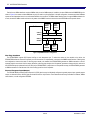
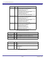
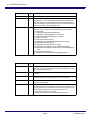
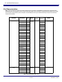
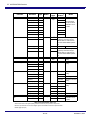
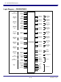
32-Lane 8-Port PCIe® Gen2 System Interconnect Switch 89HPES32NT8BG2 Datasheet ® Device Overview • All BARs support 32/64-bit base and limit address translation • Two BARs (BAR2 and BAR4) support look-up table based address translation – 32 inbound and outbound doorbell registers – 4 inbound and outbound message registers – Supports up to 64 masters – Unlimited number of outstanding transactions Multicast – Compliant with the PCI-SIG multicast – Supports 64 multicast groups – Supports multicast across non-transparent port – Multicast overlay mechanism support – ECRC regeneration support Integrated Direct Memory Access (DMA) Controllers – Supports up to 2 DMA upstream ports, each with 2 DMA channels – Supports 32-bit and 64-bit memory-to-memory transfers • Fly-by translation provides reduced latency and increased performance over buffered approach • Supports arbitrary source and destination address alignment • Supports intra- as well as inter-partition data transfers using the non-transparent endpoint – Supports DMA transfers to multicast groups – Linked list descriptor-based operation – Flexible addressing modes • Linear addressing • Constant addressing Quality of Service (QoS) – Port arbitration • Round robin – Request metering • IDT proprietary feature that balances bandwidth among switch ports for maximum system throughput – High performance switch core architecture • Combined Input Output Queued (CIOQ) switch architecture with large buffers Clocking – Supports 100 MHz and 125 MHz reference clock frequencies – Flexible port clocking modes • Common clock • Non-common clock • Local port clock with SSC (spread spectrum setting) and port reference clock input The 89HPES32NT8BG2 is a member of the IDT family of PCI Express® switching solutions. The PES32NT8BG2 is a 32-lane, 8-port system interconnect switch optimized for PCI Express Gen2 packet switching in high-performance applications, supporting multiple simultaneous peer-to-peer traffic flows. Target applications include multi-host or intelligent I/O based systems where inter-domain communication is required, such as servers, storage, communications, and embedded systems. Features High Performance Non-Blocking Switch Architecture – 32-lane, 8-port PCIe switch with flexible port configuration – Integrated SerDes supports 5.0 GT/s Gen2 and 2.5 GT/s Gen1 operation – Delivers up to 32 GBps (256 Gbps) of switching capacity – Supports 128 Bytes to 2 KB maximum payload size – Low latency cut-through architecture – Supports one virtual channel and eight traffic classes Port Configurability – Eight x4 switch ports • Adjacent x4 ports can be merged to achieve x8 port widths – Automatic per port link width negotiation (x8 --> x4 --> x2 --> x1) – Crosslink support – Automatic lane reversal – Per lane SerDes configuration • De-emphasis • Receive equalization • Drive strength Innovative Switch Partitioning Feature – Supports up to 8 fully independent switch partitions – Logically independent switches in the same device – Configurable downstream port device numbering – Supports dynamic reconfiguration of switch partitions • Dynamic port reconfiguration — downstream, upstream, non-transparent bridge • Dynamic migration of ports between partitions • Movable upstream port within and between switch partitions Non-Transparent Bridging (NTB) Support – Supports up to 8 NT endpoints per switch, each endpoint can communicate with other switch partitions or external PCIe domains or CPUs – 6 BARs per NT Endpoint • Bar address translation IDT and the IDT logo are registered trademarks of Integrated Device Technology, Inc. 1 of 35 2013 Integrated Device Technology, Inc December 17, 2013 IDT 89HPES32NT8BG2 Datasheet Hot-Plug and Hot Swap – Hot-plug controller on all ports • Hot-plug supported on all downstream switch ports – All ports support hot-plug using low-cost external I2C I/O expanders – Configurable presence-detect supports card and cable applications – GPE output pin for hot-plug event notification • Enables SCI/SMI generation for legacy operating system support – Hot-swap capable I/O Power Management – Supports D0, D3hot and D3 power management states – Active State Power Management (ASPM) • Supports L0, L0s, L1, L2/L3 Ready, and L3 link states • Configurable L0s and L1 entry timers allow performance/ power-savings tuning – SerDes power savings • Supports low swing / half-swing SerDes operation • SerDes associated with unused ports are turned off • SerDes associated with unused lanes are placed in a low power state Reliability, Availability, and Serviceability (RAS) – ECRC support – AER on all ports – SECDED ECC protection on all internal RAMs – End-to-end data path parity protection – Checksum Serial EEPROM content protected – Ability to generate an interrupt (INTx or MSI) on link up/down transitions Initialization / Configuration – Supports Root (BIOS, OS, or driver), Serial EEPROM, or SMBus switch initialization – Common switch configurations are supported with pin strapping (no external components) – Supports in-system Serial EEPROM initialization/programming On-Die Temperature Sensor – Range of 0 to 127.5 degrees Celsius – Three programmable temperature thresholds with over and under temperature threshold alarms – Automatic recording of maximum high or minimum low temperature 9 General Purpose I/O Test and Debug – Ability to inject AER errors simplifies in system error handling software validation – On-chip link activity and status outputs available for several ports – Per port link activity and status outputs available using external I2C I/O expander for all remaining ports – Supports IEEE 1149.6 AC JTAG and IEEE 1149.1 JTAG Standards and Compatibility – PCI Express Base Specification 2.1 compliant – Implements the following optional PCI Express features • Advanced Error Reporting (AER) on all ports • End-to-End CRC (ECRC) • Access Control Services (ACS) • Device Serial Number Enhanced Capability • Sub-System ID and Sub-System Vendor ID Capability • Internal Error Reporting • Multicast • VGA and ISA enable • L0s and L1 ASPM • ARI Power Supplies – Requires three power supply voltages (1.0V, 2.5V, and 3.3V) Packaged in a 23mm x 23mm 484-ball Flip Chip BGA with 1mm ball spacing Product Description With Non-Transparent Bridging functionality and innovative Switch Partitioning feature, the PES32NT8BG2 allows true multi-host or multiprocessor communications in a single device. Integrated DMA controllers enable high-performance system design by off-loading data transfer operations across memories from the processors. Each lane is capable of 5 GT/s link speed in both directions and is fully compliant with PCI Express Base Specification 2.1. A non-transparent bridge (NTB) is required when two PCI Express domains need to communicate to each other. The main function of the NTB block is to initialize and translate addresses and device IDs to allow data exchange across PCI Express domains. The major functionalities of the NTB block are summarized in Table 1. 2 of 35 December 17, 2013 IDT 89HPES32NT8BG2 Datasheet Block Diagram 8-Port Switch Core / 32 Gen2 PCI Express Lanes Frame Buffer Port Arbitration Route Table Scheduler Transaction Layer Transaction Layer Transaction Layer Data Link Layer Data Link Layer Data Link Layer Multiplexer / Demultiplexer Multiplexer / Demultiplexer Multiplexer / Demultiplexer Phy Logical Layer Phy Logical Layer Phy Logical Layer Phy Logical Layer Phy Logical Layer Phy Logical Layer Phy Logical Layer Phy Logical Layer Phy Logical Layer Phy Logical Layer Phy Logical Layer SerDes SerDes SerDes SerDes SerDes SerDes SerDes SerDes SerDes SerDes SerDes SerDes (Port 2) (Port 0) (Ports 4, 6, 8, 12, 16) Phy Logical Layer (Port 20) Figure 1 PES32NT8BG2 Block Diagram Function Number Description NTB ports Up to 8 Each device can be configured to have up to 8 NTB functions and can support up to 8 CPUs/roots. Mapping table entries Up to 64 for entire device Each device can have up to 64 masters ID for address and ID translations. Mapping windows Six 32-bits or three 64-bits Each NT port has six BARs, where each BAR opening an NT window to another domain. Address translation Direct-address and lookup table translations Lookup-table translation divides the BAR aperture into up to 24 segments, where each segment has independent translation programming and is associated with an entry in a look-up table. Doorbell registers 32 bits Doorbell register is used for event signaling between domains, where an outbound doorbell bit sets a corresponding bit at the inbound doorbell in the other domain. Message registers 4 inbound and outbound registers of 32-bits Message registers allow mailbox message passing between domains -- message placed in the inbound register will be seen at the outbound register at the other domain. Table 1 Non-Transparent Bridge Function Summary SMBus Interface The PES32NT8BG2 contains two SMBus interfaces. The slave interface provides full access to the configuration registers in the PES32NT8BG2, allowing every configuration register in the device to be read or written by an external agent. The master interface allows the default configuration register values of the PES32NT8BG2 to be overridden following a reset with values programmed in an external serial EEPROM. The master interface is also used by an external Hot-Plug I/O expander. 3 of 35 December 17, 2013 IDT 89HPES32NT8BG2 Datasheet Each of the two SMBus interfaces contain an SMBus clock pin and an SMBus data pin. In addition, the slave SMBus has the SSMBADDR2 pin. As shown in Figure 2, the master and slave SMBuses may only be used in a split configuration. In the split configuration, the master and slave SMBuses operate as two independent buses; thus, multi-master arbitration is not required. The SMBus master interface does not support SMBus arbitration. As a result, the switch’s SMBus master must be the only master in the SMBus lines that connect to the serial EEPROM and I/O expander slaves. Switch Processor SMBus Master ... Other SMBus Devices SSMBCLK SSMBDAT MSMBCLK MSMBDAT Serial EEPROM Hot-Plug I/O Expander Figure 2 Split SMBus Interface Configuration Hot-Plug Interface The PES32NT8BG2 supports PCI Express Hot-Plug on each downstream port. To reduce the number of pins required on the device, the PES32NT8BG2 utilizes an external I/O expander, such as that used on PC motherboards, connected to the SMBus master interface. Following reset and configuration, whenever the state of a Hot-Plug output needs to be modified, the PES32NT8BG2 generates an SMBus transaction to the I/O expander with the new value of all of the outputs. Whenever a Hot-Plug input changes, the I/O expander generates an interrupt which is received on the IOEXPINTN input pin (alternate function of GPIO) of the PES32NT8BG2. In response to an I/O expander interrupt, the PES32NT8BG2 generates an SMBus transaction to read the state of all of the Hot-Plug inputs from the I/O expander. General Purpose Input/Output The PES32NT8BG2 provides 9 General Purpose I/O (GPIO) pins that may be individually configured as general purpose inputs, general purpose outputs, or alternate functions. All GPIO pins are shared with other on-chip functions. These alternate functions may be enabled via software, SMBus slave interface, or serial configuration EEPROM. 4 of 35 December 17, 2013 IDT 89HPES32NT8BG2 Datasheet Pin Description The following tables list the functions of the pins provided on the PES32NT8BG2. Some of the functions listed may be multiplexed onto the same pin. The active polarity of a signal is defined using a suffix. Signals ending with an “N” are defined as being active, or asserted, when at a logic zero (low) level. All other signals (including clocks, buses, and select lines) will be interpreted as being active, or asserted, when at a logic one (high) level. Differential signals end with a suffix “N” or “P.” The differential signal ending in “P” is the positive portion of the differential pair and the differential signal ending in “N” is the negative portion of the differential pair. Note: Pin [x] of a port refers to a lane. For port 0, PE00RN[0] refers to lane 0, PE00RN[1] refers to lane 1, etc. Signal Type Name/Description PE00RN[3:0] PE00RP[3:0] I PCI Express Port 0 Serial Data Receive. Differential PCI Express receive pairs for port 0. PE00TN[3:0] PE00TP[3:0] O PCI Express Port 0 Serial Data Transmit. Differential PCI Express transmit pairs for port 0. PE02RN[3:0] PE02RP[3:0] I PCI Express Port 2 Serial Data Receive. Differential PCI Express receive pairs for port 2. PE02TN[3:0] PE02TP[3:0] O PCI Express Port 2 Serial Data Transmit. Differential PCI Express transmit pairs for port 2. PE04RN[3:0] PE04RP[3:0] I PCI Express Port 4 Serial Data Receive. Differential PCI Express receive pairs for port 4. PE04TN[3:0] PE04TP[3:0] O PCI Express Port 4 Serial Data Transmit. Differential PCI Express transmit pairs for port 4. PE06RN[3:0] PE06RP[3:0] I PCI Express Port 6 Serial Data Receive. Differential PCI Express receive pairs for port 6. PE06TN[3:0] PE06TP[3:0] O PCI Express Port 6 Serial Data Transmit. Differential PCI Express transmit pairs for port 6. PE08RN[3:0] PE08RP[3:0] I PCI Express Port 8 Serial Data Receive. Differential PCI Express receive pairs for port 8. PE08TN[3:0] PE08TP[3:0] O PCI Express Port 8 Serial Data Transmit. Differential PCI Express transmit pairs for port 8. PE12RN[3:0] PE12RP[3:0] I PCI Express Port 12 Serial Data Receive. Differential PCI Express receive pairs for port 12. PE12TN[3:0] PE12TP[3:0] O PCI Express Port 12 Serial Data Transmit. Differential PCI Express transmit pairs for port 12. PE16RN[3:0] PE16RP[3:0] I PCI Express Port 16 Serial Data Receive. Differential PCI Express receive pairs for port 16. PE16TN[3:0] PE16TP[3:0] O PCI Express Port 16 Serial Data Transmit. Differential PCI Express transmit pairs for port 16. PE20RN[3:0] PE20RP[3:0] I PCI Express Port 20 Serial Data Receive. Differential PCI Express receive pairs for port 20. PE20TN[3:0] PE20TP[3:0] O PCI Express Port 20 Serial Data Transmit. Differential PCI Express transmit pairs for port 20. Table 2 PCI Express Interface Pins 5 of 35 December 17, 2013 IDT 89HPES32NT8BG2 Datasheet Signal Type Name/Description GCLKN[1:0] GCLKP[1:0] I Global Reference Clock. Differential reference clock input pairs. This clock is used as the reference clock by on-chip PLLs to generate the clocks required for the system logic. The frequency of the differential reference clock is determined by the GCLKFSEL signal. Note: Both pairs of the Global Reference Clocks must be connected to and derived from the same clock source. Refer to the Overview section of Chapter 2 in the PES32NT8xG2 User Manual for additional details. P00CLKN P00CLKP I Port Reference Clock. Differential reference clock pair associated with port 0. P02CLKN P02CLKP I Port Reference Clock. Differential reference clock pair associated with port 2. P04CLKN P04CLKP I Port Reference Clock. Differential reference clock pair associated with port 4. Table 3 Reference Clock Pins Signal Type Name/Description MSMBCLK I/O Master SMBus Clock. This bidirectional signal is used to synchronize transfers on the master SMBus. It is active and generating the clock only when the EEPROM or I/O Expanders are being accessed. MSMBDAT I/O Master SMBus Data. This bidirectional signal is used for data on the master SMBus. SSMBADDR[2] I Slave SMBus Address. This pin determines the SMBus address to which the slave SMBus interface responds. SSMBCLK I/O Slave SMBus Clock. This bidirectional signal is used to synchronize transfers on the slave SMBus. SSMBDAT I/O Slave SMBus Data. This bidirectional signal is used for data on the slave SMBus. Table 4 SMBus Interface Pins 6 of 35 December 17, 2013 IDT 89HPES32NT8BG2 Datasheet Signal Type Name/Description GPIO[0] I/O General Purpose I/O. This pin can be configured as a general purpose I/O pin. 1st Alternate function pin name: PART0PERSTN 1st Alternate function pin type: Input/Output 1st Alternate function: Assertion of this signal initiated a partition fundamental reset in the corresponding partition. 2nd Alternate function pin name: P16LINKUPN 2nd Alternate function pin type: Output 2nd Alternate function: Port 16 Link Up Status output. GPIO[1] I/O General Purpose I/O. This pin can be configured as a general purpose I/O pin. 1st Alternate function pin name: PART1PERSTN 1st Alternate function pin type: Input/Output 1st Alternate function: Assertion of this signal initiated a partition fundamental reset in the corresponding partition. 2nd Alternate function pin name: P16ACTIVEN 2nd Alternate function pin type: Output 2nd Alternate function: Port 16 Link Active Status Output. GPIO[2] I/O General Purpose I/O. This pin can be configured as a general purpose I/O pin. 1st Alternate function pin name: PART2PERSTN 1st Alternate function pin type: Input/Output 1st Alternate function: Assertion of this signal initiated a partition fundamental reset in the corresponding partition. 2nd Alternate function pin name: P4LINKUPN 2nd Alternate function pin type: Output 2nd Alternate function: Port 4 Link Up Status output. GPIO[3] I/O General Purpose I/O. This pin can be configured as a general purpose I/O pin. 1st Alternate function pin name: PART3PERSTN 1st Alternate function pin type: Input/Output 1st Alternate function: Assertion of this signal initiated a partition fundamental reset in the corresponding partition. 2nd Alternate function pin name: P4ACTIVEN 2nd Alternate function pin type: Output 2nd Alternate function: Port 4 Link Active Status Output. GPIO[4] I/O General Purpose I/O. This pin can be configured as a general purpose I/O pin. 1st Alternate function pin name: FAILOVER0 1st Alternate function pin type: Input 1st Alternate function: When this signal changes state and the corresponding failover capability is enabled, a failover event is signaled. 2nd Alternate function pin name: P0LINKUPN 2nd Alternate function pin type: Output 2nd Alternate function: Port 0 Link Up Status output. GPIO[5] I/O General Purpose I/O. This pin can be configured as a general purpose I/O pin. 1st Alternate function pin name: GPEN 1st Alternate function pin type: Output 1st Alternate function: Hot-plug general purpose even output. 2nd Alternate function pin name: P0ACTIVEN 2nd Alternate function pin type: Output 2nd Alternate function: Port 0 Link Active Status Output. Table 5 General Purpose I/O Pins (Part 1 of 2) 7 of 35 December 17, 2013 IDT 89HPES32NT8BG2 Datasheet Signal Type Name/Description GPIO[6] I/O General Purpose I/O. This pin can be configured as a general purpose I/O pin. 1st Alternate function pin name: FAILOVER1 1st Alternate function pin type: Input 1st Alternate function: When this signal changes state and the corresponding failover capability is enabled, a failover event is signaled. 2nd Alternate function pin name: FAILOVER3 2nd Alternate function pin type: Input 2nd Alternate function: When this signal changes state and the corresponding failover capability is enabled, a failover event is signaled. GPIO[7] I/O General Purpose I/O. This pin can be configured as a general purpose I/O pin. 1st Alternate function pin name: FAILOVER2 1st Alternate function pin type: Input 1st Alternate function: When this signal changes state and the corresponding failover capability is enabled, a failover event is signaled. 2nd Alternate function pin name: P8LINKUPN 2nd Alternate function pin type: Output 2nd Alternate function: Port 8 Link Up Status output. GPIO[8] I/O General Purpose I/O. This pin can be configured as a general purpose I/O pin. 1st Alternate function pin name: IOEXPINTN 1st Alternate function pin type: Input 1st Alternate function: IO expander interrupt. 2nd Alternate function pin name: P8ACTIVEN 2nd Alternate function pin type: Output 2nd Alternate function: Port 8 Link Active Status Output. Table 5 General Purpose I/O Pins (Part 2 of 2) Signal Type Name/Description STK0CFG0 I Stack 0 Configuration. This pin selects the configuration of stack 0. STK1CFG0 I Stack 1 Configuration. This pin selects the configuration of stack 1. STK2CFG0 I Stack 2 Configuration. This pin selects the configuration of stack 2. STK3CFG0 I Stack 3 Configuration. This pin selects the configuration of stack 3. Table 6 Stack Configuration Pins Signal Type Name/Description CLKMODE[1:0] I Clock Mode. These signals determine the port clocking mode used by ports of the device. GCLKFSEL I Global Clock Frequency Select. These signals select the frequency of the GCLKP and GCLKN signals. 0x0 100 MHz 0x1 125 MHz Table 7 System Pins (Part 1 of 2) 8 of 35 December 17, 2013 IDT 89HPES32NT8BG2 Datasheet Signal Type Name/Description PERSTN I Fundamental Reset. Assertion of this signal resets all logic inside the device. RSTHALT I Reset Halt. When this signal is asserted during a switch fundamental reset sequence, the switch remains in a quasi-reset state with the Master and Slave SMBuses active. This allows software to read and write registers internal to the device before normal device operation begins. The device exits the quasi-reset state when the RSTHALT bit is cleared in the SWCTL register by an SMBus master. SWMODE[3:0] I Switch Mode. These configuration pins determine the switch operating mode. These pins should be static and not change following the negation of PERSTN. 0x0 - Single partition 0x1 - Single partition with Serial EEPROM initialization 0x2 - Single partition with Serial EEPROM Jump 0 initialization 0x3 - Single partition with Serial EEPROM Jump 1 initialization 0x4 through 0x7 - Reserved 0x8 - Single partition with reduced latency 0x9 - Single partition with Serial EEPROM initialization and reduced latency 0xA - Multi-partition with Unattached ports 0xB - Multi-partition with Unattached ports and I2C Reset 0xC - Multi-partition with Unattached ports and Serial EEPROM initialization 0xD - Multi-partition with Unattached ports with I2C Reset and Serial EEPROM initialization 0xE - Multi-partition with Disabled ports 0xF - Multi-partition with Disabled ports and Serial EEPROM initialization Table 7 System Pins (Part 2 of 2) Signal Type Name/Description JTAG_TCK I JTAG Clock. This is an input test clock used to clock the shifting of data into or out of the boundary scan logic or JTAG Controller. JTAG_TCK is independent of the system clock with a nominal 50% duty cycle. JTAG_TDI I JTAG Data Input. This is the serial data input to the boundary scan logic or JTAG Controller. JTAG_TDO O JTAG Data Output. This is the serial data shifted out from the boundary scan logic or JTAG Controller. When no data is being shifted out, this signal is tri-stated. JTAG_TMS I JTAG Mode. The value on this signal controls the test mode select of the boundary scan logic or JTAG Controller. JTAG_TRST_N I JTAG Reset. This active low signal asynchronously resets the boundary scan logic and JTAG TAP Controller. An external pull-up on the board is recommended to meet the JTAG specification in cases where the tester can access this signal. However, for systems running in functional mode, one of the following should occur: 1) actively drive this signal low with control logic 2) statically drive this signal low with an external pull-down on the board Table 8 Test Pins 9 of 35 December 17, 2013 IDT 89HPES32NT8BG2 Datasheet Signal Type Name/Description REFRES[7:0] — External Reference Resistor. Reference for the corresponding SerDes bias currents and PLL calibration circuitry. A 3K Ohm +/- 1% resistor should be connected from this pin to ground and isolated from any source of noise injection. Each bit of this signal corresponds to a SerDes quad, e.g., REFRES[5] is the reference resistor for SerDes quad 5. REFRESPLL — PLL External Reference Resistor. Provides a reference for the PLL bias currents and PLL calibration circuitry. A 3K Ohm +/- 1% resistor should be connected from this pin to ground and isolated from any source of noise injection. VDDCORE — Core VDD. Power supply for core logic (1.0V). VDDI/O — I/O VDD. LVTTL I/O buffer power supply (3.3V). VDDPEA — PCI Express Analog Power. Serdes analog power supply (1.0V). VDDPEHA — PCI Express Analog High Power. Serdes analog power supply (2.5V). VDDPETA — PCI Express Transmitter Analog Voltage. Serdes transmitter analog power supply (1.0V). VSS — Ground. Table 9 Power, Ground, and SerDes Resistor Pins 10 of 35 December 17, 2013 IDT 89HPES32NT8BG2 Datasheet Pin Characteristics Note: Some input pads of the switch do not contain internal pull-ups or pull-downs. Unused SMBus and System inputs should be tied off to appropriate levels. This is especially critical for unused control signal inputs which, if left floating, could adversely affect operation. Also, floating pins can cause a slight increase in power consumption. Unused Serdes (Rx and Tx) pins should be left floating. Finally, No Connection pins should not be connected. Function PCI Express Interface PCI Express Interface (cont.) Pin Name I/O Type Type Buffer PE00RN[3:0] I Serial Link PE00RP[3:0] I PCIe differential2 PE00TN[3:0] O PE00TP[3:0] O PE02RN[3:0] I PE02RP[3:0] I PE02TN[3:0] O PE02TP[3:0] O PE04RN[3:0] I PE04RP[3:0] I PE04TN[3:0] O PE04TP[3:0] O PE06RN[3:0] I PE06RP[3:0] I PE06TN[3:0] O PE06TP[3:0] O PE08RN[3:0] I PE08RP[3:0] I PE08TN[3:0] O PE08TP[3:0] O PE12RN[3:0] I PE12RP[3:0] I PE12TN[3:0] O PE12TP[3:0] O PE16RN[3:0] I PE16RP[3:0] I PE16TN[3:0] O PE16TP[3:0] O PE20RN[3:0] I Serial Link PE20RP[3:0] I PCIe differential PE20TN[3:0] O PE20TP[3:0] O Internal Resistor1 Notes Note: Unused SerDes pins can be left floating Table 10 Pin Characteristics (Part 1 of 2) 11 of 35 December 17, 2013 IDT 89HPES32NT8BG2 Datasheet Function Reference Clocks SMBus Pin Name Type Buffer GCLKN[1:0] I HCSL GCLKP[1:0] I P00CLKN I P00CLKP I P02CLKN I P02CLKP I P04CLKN I P04CLKP I MSMBCLK I/O MSMBDAT I/O SSMBADDR[2] I/O Type Internal Resistor1 Diff. Clock Input Notes Refer to Table 11 Note: Unused port clock pins should be connected to Vss on the board. LVTTL STI3 STI I Note: When unused, these signals must be pulled up on the board using an external resistor or current source in accordance with the SMBus specification. pull-up SSMBCLK I/O STI SSMBDAT I/O STI General Purpose I/O GPIO[8:0] I/O LVTTL STI, High Drive pull-up Unused pins can be left floating. Stack Configuration STK0CFG0 I LVTTL Input pull-down STK1CFG0 I Unused pins can be left floating. STK2CFG0 I STK3CFG0 I CLKMODE[1:0] I LVTTL Input pull-up GCLKFSEL I Unused pins can be left floating. PERSTN I RSTHALT I pull-down SWMODE[3:0] I pull-down JTAG_TCK I JTAG_TDI I JTAG_TDO O JTAG_TMS System Pins EJTAG / JTAG SerDes Reference Resistors Note: When unused, these signals must be pulled up on the board using an external resistor or current source in accordance with the SMBus specification. pull-down Schmitt trigger LVTTL STI pull-up STI pull-up I STI pull-up JTAG_TRST_N I STI pull-up REFRES[7:0] — REFRESPLL — Analog Unused pins can be left floating. Unused pins can be left floating. Unused pins should be connected to Vss on the board. Table 10 Pin Characteristics (Part 2 of 2) 1. Internal resistor values under typical operating conditions are 92K for pull-up and 91K for pull-down. 2. All receiver pins set the DC common mode voltage to ground. All transmitters must be AC coupled to the media. 3. Schmitt Trigger Input (STI). 12 of 35 December 17, 2013 IDT 89HPES32NT8BG2 Datasheet Logic Diagram — PES32NT8BG2 Global Reference Clocks GCLKN[1:0] GCLKP[1:0] GCLKFSEL PE00TP[3;0] PE00TN[3:0] PCIe Switch SerDes Output Port 0 PE02TP[3:0] PE02TN[3:0] PCIe Switch SerDes Output Port 2 PE04TP[3:0] PE04TN[3:0] PCIe Switch SerDes Output Port 4 PE04RP[3:0] PE04RN[3:0] PE06TP[3:0] PE06TN[3:0] PCIe Switch SerDes Output Port 6 PCIe Switch SerDes Input Port 6 PE06RP[3:0] PE06RN[3:0] PE08TP[3:0] PE08TN[3:0] PCIe Switch SerDes Output Port 8 PCIe Switch SerDes Input Port 8 PE08RP[3:0] PE08RN[3:0] PE12TP[3:0] PE12TN[3:0] PCIe Switch SerDes Output Port 12 PCIe Switch SerDes Input Port 12 PE12RP[3:0] PE12RN[3:0] PE16TP[3:0] PE16TN[3:0] PCIe Switch SerDes Output Port 16 PE20TP[3:0] PE20TN[3:0] PCIe Switch SerDes Output Port 20 PCIe Switch SerDes Input Port 0 PCIe Switch SerDes Input Port 2 PCIe Switch SerDes Input Port 4 PCIe Switch SerDes Input Port 16 P00CLKN P00CLKP PE00RP[3:0] PE00RN[3:0] P02CLKN P02CLKP PE02RP[3:0] PE02RN[3:0] P04CLKN P04CLKP PES32NT8BG2 PE16RP[3:0] PE16RN[3:0] 8 PCIe Switch SerDes Input Port 20 PE20RP[3:0] PE20RN[3:0] 9 Slave SMBus Interface Master SMBus Interface SSMBADDR[2] SSMBCLK SSMBDAT System Pins CLKMODE[1:0] RSTHALT PERSTN SWMODE[3:0] GPIO[8:0] JTAG_TCK JTAG_TDI JTAG_TDO JTAG_TMS JTAG_TRST_N MSMBCLK MSMBDAT STK[3:0]CFG0 REFRES[7:0] REFRESPLL SerDes Reference Resistors General Purpose I/O JTAG Pins 4 2 VDDCORE VDDI/O VDDPEA 4 Power/Ground VDDPEHA VDDPETA VSS Figure 3 PES32NT8BG2 Logic Diagram 13 of 35 December 17, 2013 IDT 89HPES32NT8BG2 Datasheet System Clock Parameters Values based on systems running at recommended supply voltages and operating temperatures, as shown in Tables 16 and 15. Parameter Description Condition Min Typical Max Unit 100 1251 MHz RefclkFREQ Input reference clock frequency range TC-RISE Rising edge rate Differential 0.6 4 V/ns TC-FALL Falling edge rate Differential 0.6 4 V/ns VIH Differential input high voltage Differential +150 VIL Differential input low voltage Differential VCROSS Absolute single-ended crossing point voltage Single-ended VCROSS-DELTA Variation of VCROSS over all rising clock edges Single-ended VRB Ring back voltage margin Differential -100 TSTABLE Time before VRB is allowed Differential 500 TPERIOD-AVG Average clock period accuracy -300 2800 ppm TPERIOD-ABS Absolute period, including spread-spectrum and jitter 9.847 10.203 ns TCC-JITTER Cycle to cycle jitter 150 ps VMAX Absolute maximum input voltage +1.15 V VMIN Absolute minimum input voltage -0.3 Duty Cycle Duty cycle 40 Rise/Fall Matching Single ended rising Refclk edge rate versus falling Refclk edge rate ZC-DC Clock source output DC impedance mV +250 -150 mV +550 mV +140 mV +100 mV ps V 60 % 20 % 40 60 Table 11 Input Clock Requirements 1. The input clock frequency will be either 100 or 125 MHz depending on signal GCLKFSEL. Note: Refclk jitter compliant to PCIe Gen2 Common Clock architecture is adequate for the GCLKN/P[x] and PE[x]CLKN/P pins of this IDT PCIe switch. This same jitter specification is applicable when interfacing the switch to another IDT switch in a Separate (Non-Common) Clock architecture. AC Timing Characteristics Parameter Gen 1 Description 1 Gen 2 Min Typ1 Max1 Min1 Typ1 Max1 399.88 400 400.12 199.94 200 200.06 Units PCIe Transmit UI Unit Interval TTX-EYE Minimum Tx Eye Width TTX-EYE-MEDIAN-to- Maximum time between the jitter median and maximum deviation from the median MAX-JITTER 0.75 0.75 0.125 ps UI UI Table 12 PCIe AC Timing Characteristics (Part 1 of 2) 14 of 35 December 17, 2013 IDT 89HPES32NT8BG2 Datasheet Parameter Gen 1 Description Min1 Typ1 Gen 2 Max1 Min1 Typ1 Max1 Units TTX-RISE, TTX-FALL TX Rise/Fall Time: 20% - 80% 0.125 0.15 UI TTX- IDLE-MIN Minimum time in idle 20 20 UI TTX-IDLE-SET-TO- Maximum time to transition to a valid Idle after sending an Idle ordered set 8 8 ns IDLE TTX-IDLE-TO-DIFF- Maximum time to transition from valid idle to diff data 8 8 ns 1.3 1.3 ns DATA TTX-SKEW Transmitter data skew between any 2 lanes TMIN-PULSED Minimum Instantaneous Lone Pulse Width NA TTX-HF-DJ-DD Transmitter Deterministic Jitter > 1.5MHz Bandwidth NA 0.15 UI TRF-MISMATCH Rise/Fall Time Differential Mismatch NA 0.1 UI 200.06 ps 0.9 UI PCIe Receive UI Unit Interval 399.88 400 400.12 TRX-EYE (with jitter) Minimum Receiver Eye Width (jitter tolerance) TRX-EYE-MEDIUM TO Max time between jitter median & max deviation 0.3 TRX-SKEW Lane to lane input skew 20 TRX-HF-RMS 1.5 — 100 MHz RMS jitter (common clock) TRX-HF-DJ-DD 0.4 199.94 0.4 UI UI MAX JITTER 8 ns NA 3.4 ps Maximum tolerable DJ by the receiver (common clock) NA 88 ps TRX-LF-RMS 10 KHz to 1.5 MHz RMS jitter (common clock) NA 4.2 ps TRX-MIN-PULSE Minimum receiver instantaneous eye width NA 0.6 UI Table 12 PCIe AC Timing Characteristics (Part 2 of 2) 1. Minimum, Typical, and Maximum values meet the requirements under PCI Express Base Specification 2.1. Signal Symbol Reference Edge Min Max Unit Timing Diagram Reference Tpw_13b2 None 50 — ns See Figure 4. GPIO GPIO[8:0]1 Table 13 GPIO AC Timing Characteristics 1. GPIO signals must meet the setup and hold times if they are synchronous or the minimum pulse width if they are asynchronous. 2. The values for this symbol were determined by calculation, not by testing. EXTCLK Tpw_13b GPIO (asynchronous input) Figure 4 GPIO AC Timing Waveform 15 of 35 December 17, 2013 IDT 89HPES32NT8BG2 Datasheet Signal Symbol Reference Edge Min Max Unit Timing Diagram Reference Tper_16a none 50.0 — ns See Figure 5. 10.0 25.0 ns 2.4 — ns 1.0 — ns — 20 ns — 20 ns 25.0 — ns JTAG JTAG_TCK Thigh_16a, Tlow_16a JTAG_TMS1, JTAG_TDI Tsu_16b JTAG_TCK rising Thld_16b JTAG_TDO Tdo_16c JTAG_TCK falling Tdz_16c2 JTAG_TRST_N Tpw_16d2 none Table 14 JTAG AC Timing Characteristics 1. The JTAG specification, IEEE 1149.1, recommends that JTAG_TMS should be held at 1 while the signal applied at JTAG_TRST_N changes from 0 to 1. Otherwise, a race may occur if JTAG_TRST_N is deasserted (going from low to high) on a rising edge of JTAG_TCK when JTAG_TMS is low, because the TAP controller might go to either the Run-Test/Idle state or stay in the Test-Logic-Reset state. 2. The values for this symbol were determined by calculation, not by testing. Tlow_16a Tper_16a Thigh_16a JTAG_TCK Thld_16b Tsu_16b JTAG_TDI Thld_16b Tsu_16b JTAG_TMS Tdo_16c Tdz_16c JTAG_TDO Tpw_16d JTAG_TRST_N Figure 5 JTAG AC Timing Waveform 16 of 35 December 17, 2013 IDT 89HPES32NT8BG2 Datasheet Recommended Operating Temperature Grade Temperature Commercial 0C to +70C Ambient Industrial -40C to +85C Ambient Table 15 PES32NT8BG2 Operating Temperatures Recommended Operating Supply Voltages — Commercial Temperature Symbol Parameter Minimum Typical Maximum Unit 0.9 1.0 1.1 V VDDCORE Internal logic supply VDDI/O I/O supply except for SerDes 3.125 3.3 3.465 V VDDPEA1 PCI Express Analog Power 0.95 1.0 1.1 V VDDPEHA2 VDDPETA1 PCI Express Analog High Power 2.25 2.5 2.75 V PCI Express Transmitter Analog Voltage 0.95 1.0 1.1 V VSS Common ground 0 0 0 V Table 16 PES32NT8BG2 Operating Voltages — Commercial Temperature VDDPEA and VDDPETA should have no more than 25mVpeak-peak AC power supply noise superimposed on the 1.0V nominal DC value. 1. 2. VDDPEHA should have no more than 50mVpeak-peak AC power supply noise superimposed on the 2.5V nominal DC value. Recommended Operating Supply Voltages — Industrial Temperature Symbol Parameter Minimum Typical Maximum Unit 0.9 1.0 1.1 V VDDCORE Internal logic supply VDDI/O I/O supply except for SerDes 3.125 3.3 3.465 V VDDPEA PCI Express Analog Power 0.95 1.0 1.05 V VDDPEHA2 VDDPETA1 PCI Express Analog High Power 2.25 2.5 2.75 V PCI Express Transmitter Analog Voltage 0.95 1.0 1.1 V VSS Common ground 0 0 0 V 1 Table 17 PES32NT8BG2 Operating Voltages — Industrial Temperature VDDPEA and VDDPETA should have no more than 25mVpeak-peak AC power supply noise superimposed on the 1.0V nominal DC value. 1. 2. VDDPEHA should have no more than 50mVpeak-peak AC power supply noise superimposed on the 2.5V nominal DC value. Power-Up/Power-Down Sequence During power supply ramp-up, VDDCORE must remain at least 1.0V below VDDI/O at all times. There are no other power-up sequence requirements for the various operating supply voltages. The power-down sequence can occur in any order. 17 of 35 December 17, 2013 IDT 89HPES32NT8BG2 Datasheet Power Consumption Typical power is measured under the following conditions: 25°C Ambient, 35% total link usage on all ports, typical voltages defined in Table 16 (and also listed below). Maximum power is measured under the following conditions: 70°C Ambient, 85% total link usage on all ports, maximum voltages defined in Table 16 (and also listed below). PCIe Analog Supply PCIe Analog High Supply Typ 1.0V Max 1.1V Typ 1.0V Max 1.1V Typ 2.5V Max 2.75V Typ 1.0V Max 1.1V Typ 3.3V Max 3.465 mA 2486 3400 1623 1806 230 234 679 729 3 5 Watts 2.49 3.74 1.62 1.99 0.58 0.64 0.68 0.80 0.01 0.02 mA 2486 3400 1396 1553 230 234 353 379 3 5 Watts 2.49 3.74 1.40 1.71 0.58 0.64 0.35 0.42 0.01 .02 Number of Active Lanes per Port x8/x8/x8/x4/x4 (Full Swing) x8/x8/x8/x4/x4 (Half Swing) PCIe Transmitter Supply Core Supply I/O Supply Total Typ Power Max Power 5.38 7.19 4.83 6.53 Table 18 PES32NT8BG2 Power Consumption Note 1: The above power consumption assumes that all ports are functioning at Gen2 (5.0 GT/S) speeds. Power consumption can be reduced by turning off unused ports through software or through boot EEPROM. Power savings will occur in VDDPEA, VDDPEHA, and VDDPETA. Power savings can be estimated as directly proportional to the number of unused ports, since the power consumption of a turnedoff port is close to zero. For example, if 3 ports out of 16 are turned off, then the power savings for each of the above three power rails can be calculated quite simply as 3/16 multiplied by the power consumption indicated in the above table. Note 2: Using a port in Gen1 mode (2.5GT/S) results in approximately 18% power savings for each power rail: VDDPEA, VDDPEHA, and VDDPETA. 18 of 35 December 17, 2013 IDT 89HPES32NT8BG2 Datasheet Thermal Considerations This section describes thermal considerations for the PES32NT8BG2 (23mm2 FCBGA484 package). The data in Table 19 below contains information that is relevant to the thermal performance of the PES32NT8BG2 switch. Symbol TJ(max) TA(max) JA(effective) JB Parameter Value Junction Temperature Ambient Temperature Effective Thermal Resistance, Junction-to-Ambient Thermal Resistance, Junction-to-Board Units Conditions 125 o Maximum 70 o Maximum for commercial-rated products 85 o C C C Maximum for industrial-rated products 15.2 o C/W Zero air flow 8.5 oC/W 1 m/S air flow 7.1 oC/W 2 m/S air flow 3.1 o C/W JC Thermal Resistance, Junction-to-Case 0.15 oC/W P Power Dissipation of the Device 7.19 Watts Maximum Table 19 Thermal Specifications for PES32NT8BG2, 23x23 mm FCBGA484 Package Note: It is important for the reliability of this device in any user environment that the junction temperature not exceed the TJ(max) value specified in Table 19. Consequently, the effective junction to ambient thermal resistance (JA) for the worst case scenario must be maintained below the value determined by the formula: JA = (TJ(max) - TA(max))/P Given that the values of TJ(max), TA(max), and P are known, the value of desired JA becomes a known entity to the system designer. How to achieve the desired JA is left up to the board or system designer, but in general, it can be achieved by adding the effects of JC (value provided in Table 19), thermal resistance of the chosen adhesive (CS), that of the heat sink (SA), amount of airflow, and properties of the circuit board (number of layers and size of the board). It is strongly recommended that users perform their own thermal analysis for their own board and system design scenarios. 19 of 35 December 17, 2013 IDT 89HPES32NT8BG2 Datasheet DC Electrical Characteristics Values based on systems running at recommended supply voltages, as shown in Table 16. Note: See Table 10, Pin Characteristics, for a complete I/O listing. I/O Type Parameter Serial Link PCIe Transmit Description Gen1 Min1 Typ1 Gen2 Max1 Min1 Typ1 Unit Max1 VTX-DIFFp-p Differential peak-to-peak output voltage 800 1200 800 1200 mV VTX-DIFFp-p-LOW Low-Drive Differential Peak to Peak Output Voltage 400 1200 400 1200 mV VTX-DE-RATIO- De-emphasized differential output voltage -3 -4 -3.0 -3.5 -4.0 dB -5.5 -6.0 -6.5 dB 3.6 V 3.5dB 6.0dB De-emphasized differential output voltage VTX-DC-CM DC Common mode voltage VTX-CM-ACP RMS AC peak common mode output voltage 20 VTX-CM-DC- Abs delta of DC common mode voltage between L0 and idle 100 100 mV Abs delta of DC common mode voltage between D+ and D- 25 25 mV delta VTX-Idle-DiffP Electrical idle diff peak output 20 20 mV RLTX-DIFF Transmitter Differential Return loss 10 10 dB 0.05 - 1.25GHz 8 dB 1.25 - 2.5GHz RLTX-CM Transmitter Common Mode Return loss 6 6 dB ZTX-DIFF-DC DC Differential TX impedance 80 120 VTX-CM-ACpp Peak-Peak AC Common 100 mV VTX-DC-CM Transmit Driver DC Common Mode Voltage 3.6 V 600 mV VTX-DE-RATIO- active-idle-delta VTX-CM-DC-line- NA Conditions 0 3.6 100 Transmitter Short Circuit Current Limit mV 120 NA 0 3.6 0 600 VTX-RCV-DETECT The amount of voltage change allowed during Receiver Detection ITX-SHORT 0 0 90 90 mA Table 20 DC Electrical Characteristics (Part 1 of 4) 20 of 35 December 17, 2013 IDT 89HPES32NT8BG2 Datasheet I/O Type Serial Link (cont.) Parameter Description Gen1 Min1 Typ1 Gen2 Max1 Min1 1200 120 Typ1 Unit Conditions Max1 PCIe Receive VRX-DIFFp-p Differential input voltage (peakto-peak) 175 RLRX-DIFF Receiver Differential Return Loss 10 RLRX-CM Receiver Common Mode Return Loss 6 ZRX-DIFF-DC Differential input impedance (DC) 80 100 ZRX--DC DC common mode impedance 40 50 ZRX-COMM-DC Powered down input common mode impedance (DC) 200k 350k ZRX-HIGH-IMP- DC input CM input impedance for V>0 during reset or power down ZRX-HIGH-IMPDC-NEG DC input CM input impedance for V<0 during reset or power down VRX-IDLE-DET- Electrical idle detect threshold DC-POS 1200 mV 10 dB 0.05 - 1.25GHz 8 65 1.25 - 2.5GHz 6 dB 120 Refer to return loss spec 60 40 60 50k 50k 50k 1.0k 1.0k 175 mV 150 mV 175 65 DIFFp-p VRX-CM-ACp Receiver AC common-mode peak voltage 150 VRX-CM-ACp PCIe REFCLK CIN Input Capacitance 1.5 — 1.5 — IOL — 2.5 IOH — IOL pF — — 2.5 — mA VOL = 0.4v -5.5 — — -5.5 — mA VOH = 1.5V — 12.0 — — 12.0 — mA VOL = 0.4v IOH — -20.0 — — -20.0 — mA VOH = 1.5V Other I/Os LOW Drive Output High Drive Output Schmitt Trigger Input (STI) VIL -0.3 — 0.8 -0.3 — 0.8 V — VIH 2.0 — VDDI/O + 0.5 2.0 — VDDI/O + 0.5 V — Input VIL -0.3 — 0.8 -0.3 — 0.8 V — VIH 2.0 — VDDI/O + 0.5 2.0 — VDDI/O + 0.5 V — 3.3V Output Low Voltage VOL — — 0.4 — 0.4 V IOL = 8mA for JTAG_TDO and GPIO pins 3.3V Output High Voltage VOH 2.4 — — — — V IOH = 8mA for JTAG_TDO and GPIO pins 2.4 Table 20 DC Electrical Characteristics (Part 2 of 4) 21 of 35 December 17, 2013 IDT 89HPES32NT8BG2 Datasheet I/O Type Parameter Capacitance CIN Description Gen1 Gen2 Min1 Typ1 Max1 Min1 Typ1 Max1 — — 8.5 — — 8.5 Unit Conditions pF — Table 20 DC Electrical Characteristics (Part 3 of 4) 22 of 35 December 17, 2013 IDT 89HPES32NT8BG2 Datasheet I/O Type Leakage Parameter Gen1 Description Gen2 Unit Conditions Min1 Typ1 Max1 Min1 Typ1 Max1 Inputs — — + 10 — — + 10 A VDDI/O (max) I/OLEAK W/O Pull-ups/downs — — + 10 — — + 10 A VDDI/O (max) I/OLEAK WITH Pull-ups/downs — — + 80 — — + 80 A VDDI/O (max) Table 20 DC Electrical Characteristics (Part 4 of 4) 1. Minimum, Typical, and Maximum values meet the requirements under PCI Express Base Specification 2.1. Absolute Maximum Voltage Rating Core Supply PCIe Analog Supply PCIe Analog High Supply PCIe Transmitter Supply I/O Supply 1.5V 1.5V 4.6V 1.5V 4.6V Table 21 PES32NT8BG2 Absolute Maximum Voltage Rating Warning: For proper and reliable operation in adherence with this data sheet, the device should not exceed the recommended operating voltages in Table 16. The absolute maximum operating voltages in Table 21 are offered to provide guidelines for voltage excursions outside the recommended voltage ranges. Device functionality is not guaranteed at these conditions and sustained operation at these values or any exposure to voltages outside the maximum range may adversely affect device functionality and reliability. SMBus Characterization Symbol Parameter SMBus 2.0 Char. Data1 3V 3.3V 3.6V Unit DC Parameter for SDA Pin VIL Input Low 1.16 1.26 1.35 V VIH Input High 1.56 1.67 1.78 V VOL@350uA Output Low 15 15 15 mV 23 24 25 mA [email protected] IPullup Current Source — — — A IIL_Leak Input Low Leakage 0 0 0 A IIH_Leak Input High Leakage 0 0 0 A Table 22 SMBus DC Characterization Data (Part 1 of 2) 23 of 35 December 17, 2013 IDT 89HPES32NT8BG2 Datasheet Symbol SMBus 2.0 Char. Data1 Parameter 3V 3.3V 3.6V Unit DC Parameter for SCL Pin VIL (V) Input Low 1.11 1.2 1.31 V VIH (V) Input High 1.54 1.65 1.76 V IIL_Leak Input Low Leakage 0 0 0 A IIH_Leak Input High Leakage 0 0 0 A Table 22 SMBus DC Characterization Data (Part 2 of 2) 1. Data at room and hot temperature. Symbol SMBus @3.3V ±10%1 Parameter Unit Min Max 5 600 KHz 3.5 — s FSCL Clock frequency TBUF Bus free time between Stop and Start THD:STA Start condition hold time 1 — s TSU:STA Start condition setup time 1 — s TSU:STO Stop condition setup time 1 — s THD:DAT Data hold time 1 — ns TSU:DAT Data setup time 1 — ns TTIMEOUT Detect clock low time out — 74.7 ms TLOW2 Clock low period 3.7 — s Clock high period 3.7 — s TF Clock/Data fall time — 72.2 ns TR Clock/Data rise time — 68.3 ns TPOR@10kHz Time which a device must be operational after power-on reset 20 — ms THIGH 2 Table 23 SMBus AC Timing Data 1. Data at room and hot temperature. 2. T LOW and THIGH are measured at FSCL = 135 kHz. 24 of 35 December 17, 2013 IDT 89HPES32NT8BG2 Datasheet Package Pinout — 484-BGA Signal Pinout for the PES32NT8BG2 The following table lists the pin numbers and signal names for the PES32NT8BG2 device. Note: Pins labeled NC are No Connection. Pin Function Alt. Pin Function Alt. Pin Function A1 VSS B5 VSS C9 VSS A2 VDDI/O B6 PE06TN1 C10 PE06RN0 A3 PE06TP3 B7 PE06TN0 C11 VSS A4 PE06TP2 B8 VSS C12 VSS A5 VSS B9 GCLKN0 C13 PE04RN3 A6 PE06TP1 B10 VSS C14 VSS A7 PE06TP0 B11 PE04TN3 C15 PE04RN2 A8 VSS B12 PE04TN2 C16 REFRES02 A9 GCLKP0 B13 VSS C17 VSS A10 VSS B14 P04CLKN C18 PE04RN0 A11 PE04TP3 B15 VSS C19 PERSTN A12 PE04TP2 B16 PE04TN1 C20 JTAG_TRST_N A13 VSS B17 PE04TN0 C21 SSMBDAT A14 P04CLKP B18 VDDI/O C22 VDDI/O A15 VSS B19 MSMBCLK D1 VSS A16 PE04TP1 B20 JTAG_TMS D2 VSS A17 PE04TP0 B21 SSMBCLK D3 VSS A18 VDDI/O B22 JTAG_TCK D4 VSS A19 MSMBDAT C1 VSS D5 PE06RP3 A20 JTAG_TDO C2 VDDI/O D6 PE06RN2 A21 CLKMODE1 C3 VSS D7 VSS A22 SSMBADDR2 C4 VSS D8 PE06RP1 B1 VSS C5 PE06RN3 D9 VSS B2 VDDI/O C6 VSS D10 PE06RP0 B3 PE06TN3 C7 VSS D11 REFRESPLL B4 PE06TN2 C8 PE06RN1 D12 VSS Alt. Table 24 PES32NT8BG2 Signal Pin-Out (Part 1 of 7) 25 of 35 December 17, 2013 IDT 89HPES32NT8BG2 Datasheet Pin Function Alt. Pin Function Alt. Pin Function D13 PE04RP3 E17 PE04RP1 F21 PE02TN2 D14 VSS E18 VDDPEHA F22 PE02TP2 D15 PE04RP2 E19 VSS G1 PE08TP0 D16 VSS E20 VSS G2 PE08TN0 D17 PE04RN1 E21 PE02TN3 G3 VSS D18 PE04RP0 E22 PE02TP3 G4 PE08RN1 D19 VSS F1 VSS G5 PE08RP1 D20 JTAG_TDI F2 VSS G6 VDDPEA D21 VDDI/O F3 PE08RN0 G7 VSS D22 VDDI/O F4 PE08RP0 G8 VDDCORE E1 VSS F5 VDDPEHA G9 VDDCORE E2 VSS F6 VDDPEHA G10 VSS E3 VSS F7 VDDPEHA G11 VDDCORE E4 VSS F8 VDDPEA G12 VDDCORE E5 VDDPEHA F9 VDDPETA G13 VSS E6 PE06RP2 F10 VDDPEA G14 VDDCORE E7 VDDPEA F11 VDDPEA G15 VDDCORE E8 VDDPEA F12 VDDPETA G16 VSS E9 VDDPETA F13 VDDPETA G17 VDDPEA E10 VDDPEA F14 VDDPEA G18 VDDPEA E11 REFRES03 F15 VDDPEA G19 PE02RP3 E12 VDDPETA F16 VDDPEA G20 PE02RN3 E13 NC F17 VDDPEHA G21 VSS E14 VSS F18 VDDPEHA G22 VSS E15 VDDPEA F19 VDDPEHA H1 PE08TP1 E16 VSS F20 VSS H2 PE08TN1 Alt. Table 24 PES32NT8BG2 Signal Pin-Out (Part 2 of 7) 26 of 35 December 17, 2013 IDT 89HPES32NT8BG2 Datasheet Pin Function Alt. Pin Function Alt. Pin Function H3 REFRES05 J7 VSS K11 VDDCORE H4 VSS J8 VDDCORE K12 VDDCORE H5 VDDPEA J9 VDDCORE K13 VSS H6 VDDPEA J10 VSS K14 VDDCORE H7 VSS J11 VDDCORE K15 VDDCORE H8 VDDCORE J12 VDDCORE K16 VSS H9 VDDCORE J13 VSS K17 VDDPETA H10 VSS J14 VDDCORE K18 REFRES01 H11 VDDCORE J15 VDDCORE K19 PE02RP1 H12 VDDCORE J16 VSS K20 PE02RN1 H13 VSS J17 VDDPETA K21 VSS H14 VDDCORE J18 VDDPETA K22 VSS H15 VDDCORE J19 REFRES00 L1 PE08TP3 H16 VSS J20 NC L2 PE08TN3 H17 VDDPEA J21 P02CLKN L3 VSS H18 PE02RP2 J22 P02CLKP L4 VSS H19 PE02RN2 K1 PE08TP2 L5 VDDPEA H20 VSS K2 PE08TN2 L6 VDDPEA H21 P00CLKN K3 VSS L7 VSS H22 P00CLKP K4 PE08RN3 L8 VDDCORE J1 VSS K5 PE08RP3 L9 VDDCORE J2 VSS K6 VDDPETA L10 VSS J3 PE08RN2 K7 VSS L11 VDDCORE J4 PE08RP2 K8 VDDCORE L12 VDDCORE J5 VDDPETA K9 VDDCORE L13 VSS J6 VDDPETA K10 VSS L14 VDDCORE Alt. Table 24 PES32NT8BG2 Signal Pin-Out (Part 3 of 7) 27 of 35 December 17, 2013 IDT 89HPES32NT8BG2 Datasheet Pin Function Alt. Pin Function Alt. Pin Function L15 VDDCORE M19 VSS P1 PE12TP1 L16 VSS M20 VSS P2 PE12TN1 L17 VDDPEA M21 PE02TN0 P3 VSS L18 PE02RP0 M22 PE02TP0 P4 VSS L19 PE02RN0 N1 PE12TP0 P5 VDDPETA L20 VSS N2 PE12TN0 P6 VDDPETA L21 PE02TN1 N3 REFRES04 P7 VSS L22 PE02TP1 N4 PE12RN1 P8 VDDCORE M1 VSS N5 PE12RP1 P9 VDDCORE M2 VSS N6 VDDPEA P10 VSS M3 PE12RN0 N7 VSS P11 VDDCORE M4 PE12RP0 N8 VDDCORE P12 VDDCORE M5 VDDPEA N9 VDDCORE P13 VSS M6 VDDPEA N10 VSS P14 VDDCORE M7 VSS N11 VDDCORE P15 VDDCORE M8 VDDCORE N12 VDDCORE P16 VSS M9 VDDCORE N13 VSS P17 VDDPEA M10 VSS N14 VDDCORE P18 PE00RP2 M11 VDDCORE N15 VDDCORE P19 PE00RN2 M12 VDDCORE N16 VSS P20 VSS M13 VSS N17 VDDPEA P21 PE00TN3 M14 VDDCORE N18 VDDPEA P22 PE00TP3 M15 VDDCORE N19 PE00RP3 R1 VSS M16 VSS N20 PE00RN3 R2 VSS M17 VDDPEA N21 VSS R3 PE12RN2 M18 VDDPEA N22 VSS R4 PE12RP2 Alt. Table 24 PES32NT8BG2 Signal Pin-Out (Part 4 of 7) 28 of 35 December 17, 2013 IDT 89HPES32NT8BG2 Datasheet Pin Function Alt. Pin Function Alt. Pin Function R5 VDDPETA T9 VDDCORE U13 VDDPEA R6 VDDPETA T10 VSS U14 VDDPEA R7 VSS T11 VDDCORE U15 VDDPETA R8 VDDCORE T12 VDDCORE U16 VDDPEA R9 VDDCORE T13 VSS U17 VDDPEHA R10 VSS T14 VDDCORE U18 PE00RP0 R11 VDDCORE T15 VDDCORE U19 PE00RN0 R12 VDDCORE T16 VSS U20 VSS R13 VSS T17 VDDPETA U21 PE00TN1 R14 VDDCORE T18 VDDPETA U22 PE00TP1 R15 VDDCORE T19 PE00RP1 V1 VDDI/O R16 VSS T20 PE00RN1 V2 VDDI/O R17 VDDPETA T21 VSS V3 PE12RN3 R18 VDDPETA T22 VSS V4 PE12RP3 R19 VSS U1 PE12TP3 V5 VSS R20 VSS U2 PE12TN3 V6 PE16RP1 R21 PE00TN2 U3 VSS V7 VSS R22 PE00TP2 U4 VSS V8 VDDPEA T1 PE12TP2 U5 VDDPEHA V9 VDDPEA T2 PE12TN2 U6 VDDPEHA V10 VSS T3 VSS U7 VDDPEA V11 VDDPETA T4 VSS U8 VDDPEA V12 VSS T5 VDDPEHA U9 VDDPEA V13 VDDPEA T6 VDDPEHA U10 VDDPETA V14 PE20RP1 T7 VSS U11 VDDPETA V15 VDDPETA T8 VDDCORE U12 VDDPEA V16 VDDPEA Alt. Table 24 PES32NT8BG2 Signal Pin-Out (Part 5 of 7) 29 of 35 December 17, 2013 IDT 89HPES32NT8BG2 Datasheet Pin Function Alt. Pin Function Alt. Pin Function Alt. V17 VDDPEHA W21 VDDI/O AA3 SWMODE0 V18 VDDPEHA W22 VDDI/O AA4 VSS V19 VSS Y1 STK0CFG0 AA5 VDDI/O V20 VSS Y2 STK3CFG0 AA6 PE16TN0 V21 PE00TN0 Y3 VSS AA7 PE16TN1 V22 PE00TP0 Y4 VDDI/O AA8 VSS W1 VSS Y5 PE16RN0 AA9 PE16TN2 W2 STK1CFG0 Y6 VSS AA10 PE16TN3 W3 STK2CFG0 Y7 VSS AA11 VSS W4 VDDI/O Y8 PE16RN2 AA12 GCLKN1 W5 PE16RP0 Y9 VSS AA13 VSS W6 PE16RN1 Y10 VSS AA14 PE20TN0 W7 REFRES06 Y11 PE16RN3 AA15 PE20TN1 W8 PE16RP2 Y12 VSS AA16 VSS W9 VSS Y13 PE20RN0 AA17 PE20TN2 W10 VSS Y14 VSS AA18 PE20TN3 W11 PE16RP3 Y15 REFRES07 AA19 VSS W12 VSS Y16 PE20RN2 AA20 GPIO_03 2 W13 PE20RP0 Y17 VSS AA21 GPIO_04 2 W14 PE20RN1 Y18 VSS AA22 GPIO_05 2 W15 VSS Y19 PE20RN3 AB1 SWMODE1 W16 PE20RP2 Y20 GPIO_06 2 AB2 RSTHALT W17 VSS Y21 GPIO_07 2 AB3 SWMODE2 W18 VDDPEHA Y22 GPIO_08 2 AB4 SWMODE3 W19 PE20RP3 AA1 CLKMODE0 AB5 VDDI/O W20 VDDI/O AA2 GCLKFSEL AB6 PE16TP0 Table 24 PES32NT8BG2 Signal Pin-Out (Part 6 of 7) 30 of 35 December 17, 2013 IDT 89HPES32NT8BG2 Datasheet Pin Function Alt. Pin Function Alt. Pin Function Alt. AB7 PE16TP1 AB13 VSS AB19 VSS AB8 VSS AB14 PE20TP0 AB20 GPIO_00 2 AB9 PE16TP2 AB15 PE20TP1 AB21 GPIO_01 2 AB10 PE16TP3 AB16 VSS AB22 GPIO_02 2 AB11 VSS AB17 PE20TP2 AB12 GCLKP1 AB18 PE20TP3 Table 24 PES32NT8BG2 Signal Pin-Out (Part 7 of 7) 31 of 35 December 17, 2013 IDT 89HPES32NT8BG2 Datasheet PES32NT8BG2 Package Drawing — 484-Pin HL/HLG484 32 of 35 December 17, 2013 IDT 89HPES32NT8BG2 Datasheet 33 of 35 Nominal package height: 2.63mm Minimum package height: 2.53mm. Note: PES32NT8BG2 Package Drawing — Page Two December 17, 2013 IDT 89HPES32NT8BG2 Datasheet Revision History October 27, 2010: Initial publication of final data sheet. November 11, 2010: Added ZB silicon on Ordering page. January 26, 2011: In Table 18, Power Consumption, revised IO (and Total) power numbers in Full Swing section and added Half Swing section. Adjusted P value in Table 19. March 9, 2011: In Table 10, deleted “External pull-down” from the Notes column for JTAG_TRST_N. March 28, 2011: In Tables 16 and 17, added VDDPETA to footnote #1. May 20, 2011: Removed ZA silicon and added ZC to Order page and codes. November 7, 2011: Revised values in Table 18, Power Consumption, and updated power dissipation value in Table 19. November 29, 2011: Added new Tables 22 and 23, SMBus Characterization and Timing. March 14, 2012: In Table 3, revised description for GCLKN/P signals. April 16, 2013: In Table 20, added 3.3V output voltage parameters under Other I/Os category. May 16, 2013: Added Note after Table 11. In Table 20, added information in the Conditions column for the 3.3V parameters. December 17, 2013: Added footnote 2 to Table 23. 34 of 35 December 17, 2013 IDT 89HPES32NT8BG2 Datasheet Ordering Information NN A Product Family Operating Voltage NNAANA Product Detail AN AA AAA Legend A = Alpha Character N = Numeric Character A Package Temp Range Generation Device Revision Series Blank I Commercial Temperature (0°C to +70°C Ambient) Industrial Temperature (-40° C to +85° C Ambient) HL 484-ball FCBGA HLG 484-ball FCBGA, Green ZB ZC ZB revision ZC revision G2 PCIe Gen 2 32NT8B 32-lane, 8-port H 1.0V Core Voltage 89 Serial Switching Product Valid Combinations 89H32NT8BG2ZBHL 484-ball FCBGA package, Commercial Temp. 89H32NT8BG2ZCHL 484-ball FCBGA package, Commercial Temp. 89H32NT8BG2ZBHLG 484-ball Green FCBGA package, Commercial Temp. 89H32NT8BG2ZCHLG 484-ball Green FCBGA package, Commercial Temp. 89H32NT8BG2ZBHLI 484-ball FCBGA package, Industrial Temp. 89H32NT8BG2ZCHLI 484-ball FCBGA package, Industrial Temp. 89H32NT8BG2ZBHLGI 484-ball Green FCBGA package, Industrial Temp. 89H32NT8BG2ZCHLGI 484-ball Green FCBGA package, Industrial Temp. ® CORPORATE HEADQUARTERS 6024 Silver Creek Valley Road San Jose, CA 95138 for SALES: 800-345-7015 or 408-284-8200 www.idt.com for Tech Support: email: [email protected] DISCLAIMER Integrated Device Technology, Inc. (IDT) and its subsidiaries reserve the right to modify the products and/or specifications described herein at any time and at IDT’s sole discretion. All information in this document, including descriptions of product features and performance, is subject to change without notice. Performance specifications and the operating parameters of the described products are determined in the independent state and are not guaranteed to perform the same way when installed in customer products. The information contained herein is provided without representation or warranty of any kind, whether express or implied, including, but not limited to, the suitability of IDT’s products for any particular purpose, an implied warranty of merchantability, or non-infringement of the intellectual property rights of others. This document is presented only as a guide and does not convey any license under intellectual property rights of IDT or any third parties. IDT’s products are not intended for use in life support systems or similar devices where the failure or malfunction of an IDT product can be reasonably expected to significantly affect the health or safety of users. Anyone using an IDT product in such a manner does so at their own risk, absent an express, written agreement by IDT. Integrated Device Technology, IDT and the IDT logo are registered trademarks of IDT. Other trademarks and service marks used herein, including protected names, logos and designs, are the property of IDT or their respective third party owners. Copyright 2013. All rights reserved. 35 of 35 December 17, 2013