1
Virtex-5 FPGA ML555
Development Kit for PCI
and PCI Express Designs
User Guide
UG201 (v1.4) March 10, 2008
R
R
Xilinx is disclosing this Document and Intellectual Property (hereinafter “the Design”) to you for use in the development of designs to operate
on, or interface with Xilinx FPGAs. Except as stated herein, none of the Design may be copied, reproduced, distributed, republished,
downloaded, displayed, posted, or transmitted in any form or by any means including, but not limited to, electronic, mechanical,
photocopying, recording, or otherwise, without the prior written consent of Xilinx. Any unauthorized use of the Design may violate copyright
laws, trademark laws, the laws of privacy and publicity, and communications regulations and statutes.
Xilinx does not assume any liability arising out of the application or use of the Design; nor does Xilinx convey any license under its patents,
copyrights, or any rights of others. You are responsible for obtaining any rights you may require for your use or implementation of the Design.
Xilinx reserves the right to make changes, at any time, to the Design as deemed desirable in the sole discretion of Xilinx. Xilinx assumes no
obligation to correct any errors contained herein or to advise you of any correction if such be made. Xilinx will not assume any liability for the
accuracy or correctness of any engineering or technical support or assistance provided to you in connection with the Design.
THE DESIGN IS PROVIDED “AS IS” WITH ALL FAULTS, AND THE ENTIRE RISK AS TO ITS FUNCTION AND IMPLEMENTATION IS
WITH YOU. YOU ACKNOWLEDGE AND AGREE THAT YOU HAVE NOT RELIED ON ANY ORAL OR WRITTEN INFORMATION OR
ADVICE, WHETHER GIVEN BY XILINX, OR ITS AGENTS OR EMPLOYEES. XILINX MAKES NO OTHER WARRANTIES, WHETHER
EXPRESS, IMPLIED, OR STATUTORY, REGARDING THE DESIGN, INCLUDING ANY WARRANTIES OF MERCHANTABILITY, FITNESS
FOR A PARTICULAR PURPOSE, TITLE, AND NONINFRINGEMENT OF THIRD-PARTY RIGHTS.
IN NO EVENT WILL XILINX BE LIABLE FOR ANY CONSEQUENTIAL, INDIRECT, EXEMPLARY, SPECIAL, OR INCIDENTAL DAMAGES,
INCLUDING ANY LOST DATA AND LOST PROFITS, ARISING FROM OR RELATING TO YOUR USE OF THE DESIGN, EVEN IF YOU
HAVE BEEN ADVISED OF THE POSSIBILITY OF SUCH DAMAGES. THE TOTAL CUMULATIVE LIABILITY OF XILINX IN CONNECTION
WITH YOUR USE OF THE DESIGN, WHETHER IN CONTRACT OR TORT OR OTHERWISE, WILL IN NO EVENT EXCEED THE
AMOUNT OF FEES PAID BY YOU TO XILINX HEREUNDER FOR USE OF THE DESIGN. YOU ACKNOWLEDGE THAT THE FEES, IF
ANY, REFLECT THE ALLOCATION OF RISK SET FORTH IN THIS AGREEMENT AND THAT XILINX WOULD NOT MAKE AVAILABLE
THE DESIGN TO YOU WITHOUT THESE LIMITATIONS OF LIABILITY.
The Design is not designed or intended for use in the development of on-line control equipment in hazardous environments requiring failsafe controls, such as in the operation of nuclear facilities, aircraft navigation or communications systems, air traffic control, life support, or
weapons systems (“High-Risk Applications”). Xilinx specifically disclaims any express or implied warranties of fitness for such High-Risk
Applications. You represent that use of the Design in such High-Risk Applications is fully at your risk.
© 2006-2008 Xilinx, Inc. All rights reserved. XILINX, the Xilinx logo, and other designated brands included herein are trademarks of Xilinx,
Inc. PCI, PCI-X, PCIe, and PCI Express are trademarks or registered trademarks of PCI-SIG. All other trademarks are the property of their
respective owners.
Revision History
The following table shows the revision history for this document.
Date
Version
Revision
09/27/06
1.0
Initial Xilinx release.
12/27/06
1.1
Changed device package to FFG1136. Inserted new Table 3-3 showing correlation
between PCIe® signals, P13 connector, FPGA pins, and GTP_DUAL tile. Revised
Chapter 3, “Hardware Description,” to reflect board design change where ICS874003-02
PCI Express® Clock Jitter attenuator module is now a customer option (added
Figure 3-8, and changed Table 3-1, Table 3-9, Table 3-18, Table 3-19, Table 3-20, and
“Serial Bus Clocking with Optional ICS874003-02 Clock Jitter Attenuator (PCI Express
Operation),” page 60). Removed Appendix A.
Virtex-5 FPGA ML555 Development Kit
www.xilinx.com
UG201 (v1.4) March 10, 2008
Date
Version
Revision
02/27/07
1.2
Changed document title and updated “Additional Documentation,” page 7. Specified
FPGA device speed grade as "-1C ES". Updated “Initial Board Checks Before Applying
Power,” page 19. Corrected board reference designator for Table 3-4, page 30 to use P1 as
PCI™ Edge Connector pinout. Updated “DDR2 SDRAM SODIMM,” page 34 to
reference DDR2 reference design included with kit. Added lane assignments to
Table 3-20, page 58. Added link to www.idt.com for availability of clock jitter attenuator
circuits on page 60. Updated Table 3-33, page 80 to include ML555 support for plugging
board into 16-lane add-in card connector. Updated Table 3-37, page 86 to include
reference designs pre-loaded into ML555 Platform Flash devices. Add Note 3 to
Table 4-1, page 89; Slave SelectMAP not supported. Updated “SelectMAP Clock
Selection” including Table 4-7 and Figure 4-8. Added reference to the Development
System Reference Guide for PROMGen and BitGen software applications. Updated
“Specifying the Xilinx PROM Device” including Figure 4-10 and Figure 4-13. Added
Figure 4-14 and Figure 4-15.
06/18/07
1.3
Updated Table 1-1, page 14 to clarify version and build information for PCI and PCI-X
IP cores. Revised Serial Bus Development section. Removed "ES" from FPGA part
number. Added footnote 3 to Table 3-3, page 27. Updated Figure 3-8, page 55 and
Figure 3-9, page 56 to include a 4.7KΩ pull-up resistor on the SATA_MGT_CLKSEL
FPGA output and labeled the Clock MUX inputs. Defined the SATA_MGT_CLKSEL
default selection in Table 3-19, page 57 for FPGA output H15. Added additional text to
footnote 6 in Table 3-20, page 58. Updated “Parallel Mode Operation,” page 62 to
indicate pressing and releasing of SW9 and SW11 to parallel load clock synthesizers after
power on to guarantee clock frequency. Updated Figure 3-14, page 76 and Table 3-34,
page 81. Added footnote 1 to Table 4-5, page 95. Updated “Generic Dynamic
Reconfiguration,” page 98 and “Platform Flash Image Generation and Programming,”
page 101 to include process steps and screen shots from ISE 9.1i. Inserted two new
figures (Figure 4-11, page 105 and Figure 4-12, page 105).
UG201 (v1.4) March 10, 2008
www.xilinx.com
Virtex-5 FPGA ML555 Development Kit
Date
Version
Revision
03/10/08
1.4
Added additional reference documents and application notes in “Additional
Documentation,” page 7. Added link to ML555 website in “About the Virtex-5 FPGA
ML555 Development Kit,” page 13. Updated “Serial Bus Development,” page 15,
including removal of Virtex-5 LogiCORE Endpoint Block Wrapper. Included Platform
USB Programming Cable and ISE Evaluation Software in “Kit Contents,” page 15.
Specified 30 MHz LVCMOS oscillator as one of three on board clock sources in “ML555
Board,” page 15. Updated Figure 3-1, page 21 to reflect “as built” 30 MHz LVCMOS
oscillator. Added reference and link to Xilinx application notes XAPP1022 and
XAPP1002 in “Edge Connector for PCI Express Operation,” page 23. Added footnote 6
to Table 3-1, page 24 to identify FPGA connection of PCIE_PERST. Added PCIE_PERST
to Table 3-3, page 27. Added reference and link to XAPP999 in “Reference Designs for
PCI and PCI-X Operation,” page 33. Added reference and links to Xilinx application
notes XAPP858 and XAPP865 in “DDR2 SDRAM SODIMM,” page 34. Corrected FPGA
pin assignments for IIC_SDA_SFP{1/2} and IIC_SCK_SFP{1/2} signals and updated
footnotes 2 and 5 in Table 3-7, page 39. Added reference and link to application note
XAPP870 in “Serial ATA Interface,” page 40. Corrected FPGA pin assignment for
P1_RCLK1 signal in Table 3-11, page 43. Added website link to download Silicon
Laboratories VCP device drivers in the “USB to UART Bridge,” page 51. Specify 30 MHz
oscillator frequency for component Y2 in Table 3-18, page 53. Changed signal name for
FPGA GCLK input pin L19 to FPGA_GCLK_30MHZ in Figure 3-8, page 55, Figure 3-9,
page 56, and Table 3-19, page 57. Changed signal name for FPGA GCLK input pin AD32
to FPGA_GCLK_30MHZ in Table 3-26, page 70. Added footnote to Table 3-37, page 86.
Updated footnote 3 in Table 4-1, page 89 to recommend Master SelectMAP configuration
of the ML555. Changed CPLD CLK to 30 MHz in Figure 4-5, page 92, Figure 4-6, page 98,
and Figure 4-7, page 99 as well as Table 4-4, page 94. Changed oscillator Y2 frequency to
30 MHz in Figure 4-8, page 100. Added footnote to Table 4-7, page 100 concerning CCLK
configuration frequency recommendation. Added BitGen command sequence to
demonstrate selection of 20 MHz CCLK configuration clock in “Platform Flash Image
Generation and Programming,” page 101.
Virtex-5 FPGA ML555 Development Kit
www.xilinx.com
UG201 (v1.4) March 10, 2008
Table of Contents
Preface: About This Guide
Guide Contents . . . . . . . . . . . . . . . . . . . . . . . . . . . . . . . . . . . . . . . . . . . . . . . . . . . . . . . . . . . . . . 7
Additional Documentation . . . . . . . . . . . . . . . . . . . . . . . . . . . . . . . . . . . . . . . . . . . . . . . . . . . 7
Additional Support Resources . . . . . . . . . . . . . . . . . . . . . . . . . . . . . . . . . . . . . . . . . . . . . . . . 9
Typographical Conventions . . . . . . . . . . . . . . . . . . . . . . . . . . . . . . . . . . . . . . . . . . . . . . . . . 10
Online Document . . . . . . . . . . . . . . . . . . . . . . . . . . . . . . . . . . . . . . . . . . . . . . . . . . . . . . . . . 11
Chapter 1: Introduction
About the Virtex-5 FPGA ML555 Development Kit . . . . . . . . . . . . . . . . . . . . . . . . . . 13
Parallel Bus Development for PCI Operation . . . . . . . . . . . . . . . . . . . . . . . . . . . . . . . . . 13
Serial Bus Development . . . . . . . . . . . . . . . . . . . . . . . . . . . . . . . . . . . . . . . . . . . . . . . . . . . 15
Kit Contents . . . . . . . . . . . . . . . . . . . . . . . . . . . . . . . . . . . . . . . . . . . . . . . . . . . . . . . . . . 15
ML555 Board . . . . . . . . . . . . . . . . . . . . . . . . . . . . . . . . . . . . . . . . . . . . . . . . . . . . . . . . . . . . . . . . 15
Available Xilinx Accessories . . . . . . . . . . . . . . . . . . . . . . . . . . . . . . . . . . . . . . . . . . . . . . .
Conversion Module, SMA to SATA (HW-AFX-SMA-SATA) . . . . . . . . . . . . . . . . . . . . .
Conversion Module, SMA to RJ45 (HW-AFX-SMA-RJ45) . . . . . . . . . . . . . . . . . . . . . . .
Conversion Module, SMA to HSSDC2 (HW-AFX-SMA-HSSDC2) . . . . . . . . . . . . . . . . .
PHY Daughtercard (HW-AFX-BERG-EPHY) . . . . . . . . . . . . . . . . . . . . . . . . . . . . . . . . .
16
16
16
17
17
Chapter 2: Getting Started
Documentation and Reference Design CD . . . . . . . . . . . . . . . . . . . . . . . . . . . . . . . . . . . 19
Initial Board Checks Before Applying Power . . . . . . . . . . . . . . . . . . . . . . . . . . . . . . . . 19
Chapter 3: Hardware Description
Edge Connector for PCI Express Operation . . . . . . . . . . . . . . . . . . . . . . . . . . . . . . . . . . 23
64-bit Edge Connector for PCI Operation . . . . . . . . . . . . . . . . . . . . . . . . . . . . . . . . . . . . 29
ML555 Configuration Headers for PCI Operation . . . . . . . . . . . . . . . . . . . . . . . . . . . . .
M66EN - 66 MHz Enable (Connector P9) . . . . . . . . . . . . . . . . . . . . . . . . . . . . . . . . . . . .
PME# - Power Management Event (Connector P7) . . . . . . . . . . . . . . . . . . . . . . . . . . . .
PCIXCAP - PCI-X Capability (Connector P8) . . . . . . . . . . . . . . . . . . . . . . . . . . . . . . . . .
Reference Designs for PCI and PCI-X Operation . . . . . . . . . . . . . . . . . . . . . . . . . . . . . .
33
33
33
33
33
DDR2 SDRAM SODIMM . . . . . . . . . . . . . . . . . . . . . . . . . . . . . . . . . . . . . . . . . . . . . . . . . . .
Small Form-factor Pluggable (SFP) Module Interface . . . . . . . . . . . . . . . . . . . . . . . .
Serial ATA Interface . . . . . . . . . . . . . . . . . . . . . . . . . . . . . . . . . . . . . . . . . . . . . . . . . . . . . . . .
SMA Connectors . . . . . . . . . . . . . . . . . . . . . . . . . . . . . . . . . . . . . . . . . . . . . . . . . . . . . . . . . . . .
Ethernet PHY Daughtercard Support . . . . . . . . . . . . . . . . . . . . . . . . . . . . . . . . . . . . . . . .
LVDS Interface . . . . . . . . . . . . . . . . . . . . . . . . . . . . . . . . . . . . . . . . . . . . . . . . . . . . . . . . . . . . .
34
39
40
41
41
44
SAMTEC Mezzanine Expansion Card Support. . . . . . . . . . . . . . . . . . . . . . . . . . . . . . . . 50
Universal Serial Bus Port . . . . . . . . . . . . . . . . . . . . . . . . . . . . . . . . . . . . . . . . . . . . . . . . . . . . 50
USB to UART Bridge . . . . . . . . . . . . . . . . . . . . . . . . . . . . . . . . . . . . . . . . . . . . . . . . . . . . . . 51
Clock Generation . . . . . . . . . . . . . . . . . . . . . . . . . . . . . . . . . . . . . . . . . . . . . . . . . . . . . . . . . . . 52
Global Clock Inputs . . . . . . . . . . . . . . . . . . . . . . . . . . . . . . . . . . . . . . . . . . . . . . . . . . . . . . . 57
Virtex-5 FPGA ML555 Development Kit
UG201 (v1.4) March 10, 2008
www.xilinx.com
5
R
GTP Reference Clock Inputs . . . . . . . . . . . . . . . . . . . . . . . . . . . . . . . . . . . . . . . . . . . . . . . . 58
Parallel Bus Clocking (PCI Operation) . . . . . . . . . . . . . . . . . . . . . . . . . . . . . . . . . . . . . . . 59
Serial Bus Clocking with Optional ICS874003-02 Clock Jitter Attenuator (PCI Express
Operation) . . . . . . . . . . . . . . . . . . . . . . . . . . . . . . . . . . . . . . . . . . . . . . . . . . . . . . . . . . . . . 60
Clock Synthesizers . . . . . . . . . . . . . . . . . . . . . . . . . . . . . . . . . . . . . . . . . . . . . . . . . . . . . . . . 61
Parallel Mode Operation . . . . . . . . . . . . . . . . . . . . . . . . . . . . . . . . . . . . . . . . . . . . . . . . . 62
Serial Mode Operation . . . . . . . . . . . . . . . . . . . . . . . . . . . . . . . . . . . . . . . . . . . . . . . . . . 68
Clock-Capable I/O Pins Associated with Clock Inputs . . . . . . . . . . . . . . . . . . . . . . . . . 70
IDELAYCTRL Reference Clock Generation . . . . . . . . . . . . . . . . . . . . . . . . . . . . . . . . . . . 72
User LEDs . . . . . . . . . . . . . . . . . . . . . . . . . . . . . . . . . . . . . . . . . . . . . . . . . . . . . . . . . . . . . . . . . .
Configuration INIT and DONE LEDs . . . . . . . . . . . . . . . . . . . . . . . . . . . . . . . . . . . . . . .
User Pushbutton Switches . . . . . . . . . . . . . . . . . . . . . . . . . . . . . . . . . . . . . . . . . . . . . . . . . . .
Pushbutton Program Switch (SW6) . . . . . . . . . . . . . . . . . . . . . . . . . . . . . . . . . . . . . . . . . .
Pushbutton Reset Switch (SW7) . . . . . . . . . . . . . . . . . . . . . . . . . . . . . . . . . . . . . . . . . . . . .
Power Consumption . . . . . . . . . . . . . . . . . . . . . . . . . . . . . . . . . . . . . . . . . . . . . . . . . . . . . . . .
Voltage Regulators . . . . . . . . . . . . . . . . . . . . . . . . . . . . . . . . . . . . . . . . . . . . . . . . . . . . . . . . . .
ML555 DC Power System . . . . . . . . . . . . . . . . . . . . . . . . . . . . . . . . . . . . . . . . . . . . . . . . . .
PCI and/or PCI-X Application Add-in Card Power Input . . . . . . . . . . . . . . . . . . . . . .
Add-in Card DC Power Input (PCI Express Operation) . . . . . . . . . . . . . . . . . . . . . . . .
ML555 Board DC Power Regulators . . . . . . . . . . . . . . . . . . . . . . . . . . . . . . . . . . . . . . . . .
GTP Transceiver Power. . . . . . . . . . . . . . . . . . . . . . . . . . . . . . . . . . . . . . . . . . . . . . . . . . . .
DDR2 SODIMM Power . . . . . . . . . . . . . . . . . . . . . . . . . . . . . . . . . . . . . . . . . . . . . . . . . . . .
Power Supply Monitoring . . . . . . . . . . . . . . . . . . . . . . . . . . . . . . . . . . . . . . . . . . . . . . . . .
ML555 Board Physical Dimensions . . . . . . . . . . . . . . . . . . . . . . . . . . . . . . . . . . . . . . . . . .
73
73
74
74
74
74
75
75
79
80
80
82
82
82
85
XC2C32 CoolRunner-II CPLD U6 . . . . . . . . . . . . . . . . . . . . . . . . . . . . . . . . . . . . . . . . . . . . 85
XCF32PFS48C Platform Flash U1 and U15 . . . . . . . . . . . . . . . . . . . . . . . . . . . . . . . . . . . 86
Chapter 4: Configuration
Configuration Modes . . . . . . . . . . . . . . . . . . . . . . . . . . . . . . . . . . . . . . . . . . . . . . . . . . . . . . .
JTAG Chain . . . . . . . . . . . . . . . . . . . . . . . . . . . . . . . . . . . . . . . . . . . . . . . . . . . . . . . . . . . . . . . . .
JTAG Port. . . . . . . . . . . . . . . . . . . . . . . . . . . . . . . . . . . . . . . . . . . . . . . . . . . . . . . . . . . . . . . . . . .
SelectMAP Interface . . . . . . . . . . . . . . . . . . . . . . . . . . . . . . . . . . . . . . . . . . . . . . . . . . . . . . . .
89
89
90
91
CPLD Programming Examples . . . . . . . . . . . . . . . . . . . . . . . . . . . . . . . . . . . . . . . . . . . . . 97
Static Configuration . . . . . . . . . . . . . . . . . . . . . . . . . . . . . . . . . . . . . . . . . . . . . . . . . . . . 97
Generic Dynamic Reconfiguration . . . . . . . . . . . . . . . . . . . . . . . . . . . . . . . . . . . . . . . . . 98
SelectMAP Clock Selection . . . . . . . . . . . . . . . . . . . . . . . . . . . . . . . . . . . . . . . . . . . . . . . . . 100
Platform Flash Image Generation and Programming . . . . . . . . . . . . . . . . . . . . . . . . 101
Setup . . . . . . . . . . . . . . . . . . . . . . . . . . . . . . . . . . . . . . . . . . . . . . . . . . . . . . . . . . . . . . . . . .
Creating a PROM File in Command Line Mode . . . . . . . . . . . . . . . . . . . . . . . . . . . . . .
iMPACT and PROMGEN Wizard GUI Mode . . . . . . . . . . . . . . . . . . . . . . . . . . . . . . . .
Specifying the Xilinx PROM Device . . . . . . . . . . . . . . . . . . . . . . . . . . . . . . . . . . . . . . . .
Programming the PROM . . . . . . . . . . . . . . . . . . . . . . . . . . . . . . . . . . . . . . . . . . . . . . . . .
6
www.xilinx.com
101
101
101
103
104
Virtex-5 FPGA ML555 Development Kit
UG201 (v1.4) March 10, 2008
R
Preface
About This Guide
This user guide is a description of the Virtex™-5 FPGA ML555 Development Kit for PCI™
and PCI Express® designs. Complete and up-to-date documentation of the Virtex-5 family
of FPGAs is available on the Xilinx website at http://www.xilinx.com/virtex5.
Guide Contents
This manual contains the following chapters:
•
Chapter 1, “Introduction”
•
Chapter 2, “Getting Started”
•
Chapter 3, “Hardware Description”
•
Chapter 4, “Configuration”
Additional Documentation
The following documents are also available for download at
http://www.xilinx.com/virtex5.
•
Virtex-5 Family Overview
The features and product selection of the Virtex-5 family are outlined in this overview.
•
Virtex-5 Data Sheet: DC and Switching Characteristics
This data sheet contains the DC and Switching Characteristic specifications for the
Virtex-5 family.
•
Virtex-5 FPGA User Guide
This user guide includes chapters on:
♦
Clocking Resources
♦
Clock Management Technology (CMT)
♦
Phase-Locked Loops (PLLs)
♦
Block RAM and FIFO memory
♦
Configurable Logic Blocks (CLBs)
♦
SelectIO™ Resources
♦
I/O Logic Resources
♦
Advanced I/O Logic Resources
Virtex-5 FPGA ML555 Development Kit
UG201 (v1.4) March 10, 2008
www.xilinx.com
7
R
Preface: About This Guide
•
Virtex-5 FPGA RocketIO GTP Transceiver User Guide
This user guide describes the RocketIO™ GTP transceivers available in the Virtex-5
LXT and SXT platform devices.
•
Virtex-5 FPGA Embedded Tri-Mode Ethernet MAC User Guide
This user guide describes the dedicated Tri-Mode Ethernet Media Access Controller
available in the Virtex-5 LXT and SXT platform devices.
•
Virtex-5 Integrated Endpoint Block User Guide for PCI Express Designs
This user guide describes the integrated Endpoint blocks in the Virtex-5 LXT and SXT
platform devices for PCI Express® designs.
•
Virtex-5 FPGA XtremeDSP Design Considerations
This guide describes the XtremeDSP™ slice and includes reference designs for using
the DSP48E.
•
Virtex-5 FPGA Configuration Guide
This all-encompassing configuration guide includes chapters on configuration
interfaces (serial and SelectMAP), bitstream encryption, Boundary-Scan and JTAG
configuration, reconfiguration techniques, and readback through the SelectMAP and
JTAG interfaces.
•
Virtex-5 FPGA System Monitor User Guide
The System Monitor functionality available in all the Virtex-5 devices is outlined in
this guide.
•
Virtex-5 FPGA Packaging Specifications
This specification includes the tables for device/package combinations and maximum
I/Os, pin definitions, pinout tables, pinout diagrams, mechanical drawings, and
thermal specifications.
•
Virtex-5 PCB Designer’s Guide
This guide provides information on PCB design for Virtex-5 devices, with a focus on
strategies for making design decisions at the PCB and interface level.
The following documents provide supplemental material useful to this user guide:
1.
DS090, CoolRunner-II CPLD Family
2.
DS123, Platform Flash In-System Programmable Configuration PROMs
3.
UG065, PHY Daughter Card User Guide
4.
XAPP938, Dynamic Bus Mode Reconfiguration of PCI-X and PCI Designs
5.
XAPP1022, Using the Memory Endpoint Test Driver (MET) with the Programmed Input/Output
Example Design for PCI Express Endpoint Cores
6.
XAPP1002, Using ChipScope Pro to Debug Endpoint Block Plus Wrapper, Endpoint, and Endpoint
PIPE Designs for PCI Express
7.
XAPP999, Reference System: PLBv46 PCI Using the ML555 Embedded Development Platform
8.
XAPP858, High-Performance DDR2 SDRAM Interface in Virtex-5 Devices
9.
XAPP865, Hardware Accelerator for RAID6 Parity Generation / Data Recovery Controller with
ECC and MIG DDR2 Controller
10. UG086, Xilinx Memory Interface Generator (MIG) User Guide
11. XAPP870, Serial ATA Physical Link Initialization with the GTP Transceiver of Virtex-5 LXT
FPGAs
8
www.xilinx.com
Virtex-5 FPGA ML555 Development Kit
UG201 (v1.4) March 10, 2008
R
Additional Support Resources
12. XAPP693, A CPLD-Based Configuration and Revision Manager for Xilinx Platform Flash PROMs
and FPGAs
The Endpoint Block Plus for PCI Express solution from Xilinx is a reliable, highbandwidth, scalable serial interconnect building block for use with the Virtex-5 LXT and
SXT platform FPGAs. The core instantiates the Virtex-5 FPGA Integrated Block for PCI
Express designs found in the Virtex-5 LXT and SXT devices. The Endpoint Block Plus core
is a Xilinx CORE Generator™ IP core included in the latest IP Update on the Xilinx IP
Center. Included with the Xilinx IP are a data sheet, a getting started guide, and a user
guide. These documents are generated by the CORE Generator tool when starting a design
project. The documents can be downloaded from the Xilinx website at:
http://www.xilinx.com/support/documentation/ip_documentation/pcie_blk_plus_ds551.pdf
http://www.xilinx.com/support/documentation/ip_documentation/pcie_blk_plus_gsg343.pdf
http://www.xilinx.com/support/documentation/ip_documentation/pcie_blk_plus_ug341.pdf
Additional technical information on PCI Express solutions is available at:
http://www.xilinx.com/pciexpress
Xilinx provides customizable LogiCORE™ Initiator/Target cores for PCI and PCI-X
applications designed to work with Virtex-5 FPGAs. Included with the Xilinx IP are a data
sheet, getting started guide, and user guide. These documents are generated by the CORE
Generator tool when starting a design project. Additional information is available on the
Xilinx website at:
http://www.xilinx.com/products/design_resources/conn_central/protocols/pci_pcix.htm
PCI, PCI-X™, and PCI Express specifications are available from the PCI Special Interest
Group (PCISIG). Contact the PCI Special Interest Group office to obtain the latest revision
of these specifications. Questions regarding the PCI Local Bus Specification or the PCI-X
Addendum or membership in the PCI Special Interest Group can be forwarded through:
PCI Special Interest Group (PCI-SIG)
5440 SW Westgate Dr., #217
Portland, OR 97221
Phone: 800-433-5177 (inside the U.S.), 503-291-2569 (outside the U.S.)
Fax: 503-297-1090
e-mail: [email protected]
Website: http://www.pcisig.com
•
PCI Local Bus Specification, Revision 3.0
•
PCI-X Addendum to the PCI Local Bus Specification
•
PCI Express Base Specification
•
PCI Express Card Electromechanical Specification
Additional Support Resources
To search the database of silicon and software questions and answers, or to create a
technical support case in WebCase, see the Xilinx website at:
http://www.xilinx.com/support.
Virtex-5 FPGA ML555 Development Kit
UG201 (v1.4) March 10, 2008
www.xilinx.com
9
R
Preface: About This Guide
Typographical Conventions
This document uses the following typographical conventions. An example illustrates each
convention.
Convention
Italic font
Underlined Text
10
Meaning or Use
Example
See the Virtex-5 FPGA
References to other documents Configuration Guide for more
information.
Emphasis in text
The address (F) is asserted after
clock event 2.
Indicates a link to a web page.
http://www.xilinx.com/virtex5
www.xilinx.com
Virtex-5 FPGA ML555 Development Kit
UG201 (v1.4) March 10, 2008
R
Typographical Conventions
Online Document
The following conventions are used in this document:
Convention
Meaning or Use
Example
See the section “Additional
Documentation” for details.
Blue text
Cross-reference link to a location
in the current document
Red text
Cross-reference link to a location
in another document
See Figure 5 in the Virtex-5 FPGA
Data Sheet
Blue, underlined text
Hyperlink to a website (URL)
Go to http://www.xilinx.com
for the latest documentation.
Virtex-5 FPGA ML555 Development Kit
UG201 (v1.4) March 10, 2008
www.xilinx.com
Refer to “Clock Management
Technology (CMT)” in
Chapter 2 for details.
11
R
Preface: About This Guide
12
www.xilinx.com
Virtex-5 FPGA ML555 Development Kit
UG201 (v1.4) March 10, 2008
R
Chapter 1
Introduction
About the Virtex-5 FPGA ML555 Development Kit
To develop parallel Peripheral Component Interconnect (PCI™) bus and serial PCI
Express® bus add-in card applications, the Virtex™-5 FPGA ML555 board is configured
and then plugged into a parallel PCI bus system unit or a serial PCI Express system unit.
The board supports 32-bit or 64-bit PCI bus datapaths. The ML555 board has an eight-lane
connector that allows the board to be plugged into an eight-lane add-in card socket for PCI
Express operation. The ML555 kit does not include a lane conversion adapter, which
would allow the eight-lane ML555 board to plug into an add-in card socket for single-lane
PCI Express operation.
Additional information and design resources associated with the ML555 development kit
is available at:
http://www.xilinx.com/products/devkits/HW-V5-ML555-G.htm
Parallel Bus Development for PCI Operation
This Virtex-5 FPGA based kit provides a development platform for designing and
verifying PCI and PCI-X™ applications utilizing Xilinx LogiCORE™ intellectual property
(IP) cores in a 3.3V signaling environment. The ML555 board is intended to plug-in to a
3.3V keyed system board. The ML555 board is not a Universal add-in card nor is it
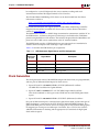
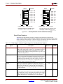
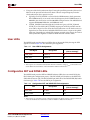
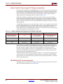
intended to plug into a 5V keyed system board. Figure 1-1 shows how to identify a 3.3V
system board slot (left side) from a non-supported 5V system board slot (right side).
Dual Voltage Signalling
Add-in Card
I/O Buffers Powered on
Connector Dependent Rail
3.3V 64-bit Connector
Figure 1-1:
Virtex-5 FPGA ML555 Development Kit
UG201 (v1.4) March 10, 2008
Rear of
Computer Chassis
Rear of
Computer Chassis
3.3V Add-in Card
I/O Buffers Powered
on 3.0V Rail
5V 64-bit Connector
UG201_c1_01_050106
Add-in Card Connectors
www.xilinx.com
13
R
Chapter 1: Introduction
The ML555 board is supported by Xilinx LogiCORE IP versions 4 and 6, respectively. Each
core has a primary version number, shown in Table 1-1, followed by a revision or build
number. More information about the current versions of these cores is available in the
LogiCORE data sheets for the PCI and PCI-X section of the PCI/PCI-X product lounge
(refer to http://www.xilinx.com/products/logicore/lounge/lounge.htm). Table 1-1 lists
the Xilinx cores for PCI and PCI-X operation.
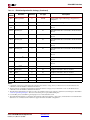
Table 1-1:
Xilinx Cores Supporting PCI and PCI-X Operation
Version
Bus
Mode
Bus Width
Clock
Frequency
Clock Type
(FPGA Pin #)
v4
PCI
32 bits
33 MHz
Global (J14)
v4
PCI
32 bits
66 MHz
Global (J14)
v4
PCI
64 bits
33 MHz
Global (J14)
v6
PCI-X
64 bits
133 MHz
Global (J14)
v6
PCI-X
64 bits
100 MHz
Global (J14)
v6
PCI-X
64 bits
66 MHz
Global (J14)
v6
PCI
64 bits
33 MHz
Global (J14)
These Xilinx interface cores are pre-implemented and fully tested modules for Xilinx
FPGAs.
The v4 64-bit interface is compliant with the PCI Local Bus Specification, revision 3.0. The
v6 64-bit interface is compliant with the PCI Local Bus Specification, revision 3.0, and the
PCI-X Addendum, revision 2.0.
The pinout for each Virtex-5 device and the relative placement of the internal logic are
predefined. Critical paths are controlled by constraints to ensure predictable timing,
significantly reducing the engineering time required to implement the bus interface
portion of a user design. When targeting an XC5VLX50T-FFG1136 FPGA, the Xilinx CORE
Generator™ tool provides an example design and a constraints file utilizing the ML555
board pinout for PCI and PCI-X designs.
Resources can instead be focused on unique user application logic in the FPGA and on the
system-level design. As a result, the Xilinx interface products for PCI and PCI-X operation
minimize product development time.
The following links provide more information:
•
Xilinx LogiCORE products:
www.xilinx.com/products/design_resources/conn_central/index.htm
•
PCI and PCI-X specific applications:
www.xilinx.com/products/design_resources/conn_central/protocols/pci_pcix.htm
Included with the purchase of the ML555 development kit is a 90-day access to full system
hardware evaluation versions of the Virtex-5 FPGA LogiCORE products for PCI and PCI-X
designs. The following link provides additional information specific to the ML555 board
and LogiCORE products:
www.xilinx.com/ipcenter/ml555/ml555_eval_instr.htm
14
www.xilinx.com
Virtex-5 FPGA ML555 Development Kit
UG201 (v1.4) March 10, 2008
R
ML555 Board
Serial Bus Development
The ML555 board is supported by a LogiCORE endpoint wrapper to configure the
Integrated Endpoint Block for PCI Express operation in Virtex-5 LXT and SXT FPGAs:
•
Virtex-5 FPGA LogiCORE Endpoint Block Plus Wrapper for PCI Express designs
This is the recommended wrapper for PCI Express designs. It provides many ease-ofuse features and optimal configuration for Endpoint applications while simplifying
the design process and reducing the time-to-market.
The endpoint solution is delivered through the Xilinx CORE Generator tool. Full access to
the core, including bitstream generation capability, can be obtained through registration at
no extra charge.
Additional technical information on Xilinx PCI Express solutions is available at:
www.xilinx.com/pciexpress
Refer to UG197, Virtex-5 Integrated Endpoint Block User Guide for PCI Express Designs for
more information on the integrated Endpoint solution.
Kit Contents
The ML555 board kit includes the following:
•
Virtex-5 FPGA ML555 board (XC5VLX50T-FFG1136C-1 speed grade FPGA)
•
Documentation and reference design CD
•
Time-out evaluation licenses for the LogiCORE IP for PCI and PCI-X designs
•
Drivers for Jungo Software Technologies WinDriver device driver development kit
can be downloaded from www.jungo.com/dnload.html and evaluated for 60 days
•
Xilinx Platform Cable USB programming cable
•
ISE™ evaluation software
For assistance with any of these items, contact your local Xilinx distributor or visit the
Xilinx online store at www.xilinx.com.
The heart of the kit is the ML555 board. This manual provides comprehensive information
on this board.
ML555 Board
The ML555 board includes the following:
•
XC5VLX50T-FFG1136C -1 speed grade FPGA
•
200-pin 1.8V SODIMM socket with 256 MB (32M x 64 bit) DDR2 SDRAM SODIMM
•
Three on-board clock sources, two differential SMA clock inputs, and two
programmable clock synthesizers:
♦
30 MHz LVCMOS
♦
125 and 200 MHz Epson 2.5V EG-2121CA LVDS and LVPECL, respectively
•
One Universal Serial Bus (USB) 2.0 port (USB interface cable not provided)
•
Support for up to four FPGA design images in two Xilinx XCF32P-FSG48C Platform
Flash configuration PROM devices
•
Static or dynamic device reconfiguration support with the XC2C32 CoolRunner™ II
CPLD
Virtex-5 FPGA ML555 Development Kit
UG201 (v1.4) March 10, 2008
www.xilinx.com
15
R
Chapter 1: Introduction
•
64-bit 3.3V system board keyed connector for PCI or PCI-X operation
•
Support for Endpoint designs in x1, x4, and x8 lane configurations
•
Two Small Form-factor Pluggable (SFP) Transceiver module ports (SFP modules are
not included)
•
Xilinx Generic Interface (XGI) headers support installation of Xilinx Ethernet PHY
daughtercard (sold separately) for 10/100/1000 Mb Ethernet connectivity
•
Two SAMTEC LVDS interface connectors with up to 24 high-speed LVDS channels
each (cables sold separately)
•
One Serial ATA (SATA) disk drive interface connector (SATA cable not provided)
•
One set of SMA ports for offboard GTP transceiver connectivity
•
User pushbutton switches and LEDs
•
Device configuration through on-board Platform Flash or Xilinx Platform Cable USB
•
PCI clocking support for global and regional clocking applications
•
On-board power regulators (3.0V PCI, 2.5V, 1.8V, 1.0V, 0.9V VTT)
•
Two programmable clock synthesizer chips to support DDR2 memory interfaces,
10/100/1000 Mb Ethernet protocols, SATA, Fibre Channel, Aurora, and other serial
GTP baud rates
Available Xilinx Accessories
The ML555 board has one set of SMA connectors connected to one of the GTP transceiver
ports of the XC5VLX50T FPGA. Xilinx sells a number of SMA conversion module boards
that permit the conversion of the on-board SMA interface to other popular multi-gigabit
serial connector interfaces. These accessories boards are available through your local Xilinx
Sales office.
Xilinx also provides an Ethernet PHY daughtercard that can be used to provide dual
Ethernet connectivity to the ML555 development kit.
Note: Not all accessories are RoHS compliant, and they might not be available in all countries.
Contact your local Xilinx Sales office to determine product availability.
Conversion Module, SMA to SATA (HW-AFX-SMA-SATA)
The SMA to SATA module can be used in conjunction with the ML555 SMA connectors.
The ML555 only provides one set of SMA connectors, whereas the HW-AFX-SMA-SATA
conversion module contains two sets of SMA connectors and two SATA connectors. DC
power is not provided to the SATA disk drive from either the ML555 board or the
conversion module.
The SMA to SATA conversion module can be ordered from Xilinx as part number
HW-AFX-SMA-SATA. Contact your local sales office for pricing information. Additional
information on the conversion module is available from the Xilinx website at:
www.xilinx.com/xlnx/xebiz/designResources/ip_product_details.jsp?key=HW-AFX-SMA-SATA
Conversion Module, SMA to RJ45 (HW-AFX-SMA-RJ45)
The SMA to RJ45 module can be used in conjunction with the ML555 SMA connectors to
convert the SMA interface to a RJ45 interface. This adapter does not support
10/100/1000BASE-T applications.
16
www.xilinx.com
Virtex-5 FPGA ML555 Development Kit
UG201 (v1.4) March 10, 2008
R
ML555 Board
The SMA to RJ45 conversion module can be ordered from Xilinx as part number HW-AFXSMA-RJ45. Contact your local sales office for pricing information. Additional information
on the conversion module is available from the Xilinx website at:
www.xilinx.com/xlnx/xebiz/designResources/ip_product_details.jsp?key=HW-AFX-SMA-RJ45
Conversion Module, SMA to HSSDC2 (HW-AFX-SMA-HSSDC2)
The SMA to HSSDC2 module can be used in conjunction with the ML555 SMA connectors
to convert the SMA interface to a HSSDC2 interface.
The SMA to HSSDC2 conversion module can be ordered from Xilinx as part number HWAFX-SMA-HSSDC2. Contact your local sales office for pricing information. Additional
information on the conversion module is available from the Xilinx website at:
www.xilinx.com/xlnx/xebiz/designResources/ip_product_details.jsp?key=HW-AFX-SMA-HSSDC2
PHY Daughtercard (HW-AFX-BERG-EPHY)
The PHY daughtercard plugs into the XGI headers on the ML555 board. The PHY
daughtercard provides Ethernet capability to the ML555 development platform by using
two Marvel Alaska 88E1111 Gigabit over copper transceivers. These PHY devices perform
all physical layer (PHY) functions, operate at 10/100/1000 Mb/s and support many
interfaces of the embedded tri-mode Ethernet MAC in the Virtex-5 FPGA.
The PHY daughtercard can be ordered from Xilinx as part number HW-AFX-BERG-EPHY.
Contact your local sales office for pricing information. Additional information on the PHY
daughtercard is available from the Xilinx website at:
www.xilinx.com/xlnx/xebiz/designResources/ip_product_details.jsp?key=HW-AFX-BERG-EPHY
Virtex-5 FPGA ML555 Development Kit
UG201 (v1.4) March 10, 2008
www.xilinx.com
17
R
Chapter 1: Introduction
18
www.xilinx.com
Virtex-5 FPGA ML555 Development Kit
UG201 (v1.4) March 10, 2008
R
Chapter 2
Getting Started
This chapter describes the items needed to configure the Virtex-5 FPGA ML555 board. The
ML555 board is tested prior to shipment and should work out of the box. The installer is
recommended to inspect the board prior to use and confirm proper jumper and switch
settings as directed in this user guide.
The ML555 board must be plugged into either a parallel bus expansion slot for PCI systems
or a serial system bus expansion slot for PCI Express systems. The DC power provided to
the ML555 board from the PCI Express and PCI buses is different. The ML555 system
power configuration must be properly configured through board headers and shunts prior
to plugging into the system unit. Failure to configure the ML555 DC power system might
result in damage to the ML555 board or the system unit.
Contact Xilinx Technical Support with any questions about proper configuration of the
ML555 prior to powering up a system at:
http://www.xilinx.com/support/clearexpress/websupport.htm
Documentation and Reference Design CD
The CD included in the Virtex-5 FPGA ML555 board kit contains the board design files,
including schematics, PCB layout, and bill of materials. FPGA and CPLD design constraint
files are included on the CD. This file provides a signal listing and physical FPGA pin
locations (LOC) constraint to get started designing user applications with the Xilinx ISE
software. Signal names can be changed to match user preferences if the board schematic
signal names are not identical to the top-level user design file names. Open the
ReadMe.txt file on the CD to review the list of contents.
Initial Board Checks Before Applying Power
Note: These steps MUST be performed before plugging in the ML555 board:
1.
Set up the Configuration Mode Switch SW5 for Master SelectMAP. See Table 4-1,
page 89 and Figure 4-2, page 89.
2.
Configure Jumper Block P2 to select configuration CCLK source (FPGA). See
Table 4-7, page 100 and Figure 4-8, page 100.
3.
Configure Jumper Block P3 to select one of four Platform Flash configuration files or
use JTAG programming cable to load user design. See Table 3-37, page 86.
4.
Switch SW8: selects the FPGA VCCINT source (PCI or PCI Express bus) as described in
“ML555 DC Power System,” page 75.
5.
Jumper Block P18: enables the 12V to 5V enable for PCI Express operation as described
in “ML555 DC Power System,” page 75.
The ML555 board now can be plugged into a powered down 3.3V (only) add-in card slot
for PCI Express or PCI/PCI-X operation. See the cd_rom.txt file on the CD.
Virtex-5 FPGA ML555 Development Kit
UG201 (v1.4) March 10, 2008
www.xilinx.com
19
R
Chapter 2: Getting Started
20
www.xilinx.com
Virtex-5 FPGA ML555 Development Kit
UG201 (v1.4) March 10, 2008
R
Chapter 3
Hardware Description
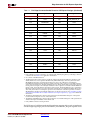
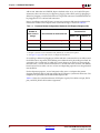
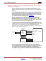
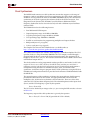
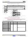
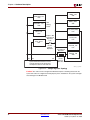
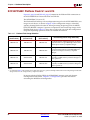
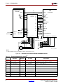
A high-level block diagram of the Virtex-5 FPGA ML555 board is shown in Figure 3-1,
followed by a brief description of each board section. Figure 3-2 is a photograph of the
ML555 board with the key interfaces marked.
Serial ATA
Connector (J5)
GTP SMA
Connectors
DDR2
SODIMM (J2)
SFP Connectors
(x2)
(J3 and J4)
125 and 200 MHz
Oscillators
Xilinx Generic
Interface (XGI)
Header
(Ethernet PHY)
Programmable
Clock
Synthesizer (x2)
Parallel Cable IV
JTAG Port (P5)
Virtex-5
FPGA
XC5VLX50T
(FFG1136)
30 MHz
LVCMOS
Oscillator
Clock Generator
32 Mbit
XCF32P
Platform Flash (x2)
Xilinx
XC2C32
CPLD
USB 2.0 Port
(J1)
3.0V for
PCI Compliance
24-Channel LVDS
I/O Interfaces
(x2)
(P32 and P33)
System 2.5V
System 1.8V
VCCINT 1.0V
64-bit 3.3V
Edge Connector
for PCI/PCI-X (P1)
VTT 0.9V
GTP Analog Power
x1, x4, or x8
Edge Connector
for PCI Express
(P13)
Voltage Regulators
UG201_c3_01_030508
Figure 3-1:
Virtex-5 FPGA ML555 Development Kit
UG201 (v1.4) March 10, 2008
ML555 Board Block Diagram
www.xilinx.com
21
R
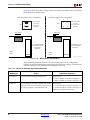
Chapter 3: Hardware Description
J2:
DDR2
SODIMM
J15/J16:
Xilinx Generic Interface
Headers
XC5VLX50T FPGA
GTP SMA
MGTREFCLK
GTP SMA
P32: LVDS
P33: LVDS
P1: Bus
Connector for
PCI/PCI-X
Designs
P13: Connector
for PCI Express
Designs
P5: JTAG
Configuration
Global
CLK SMA
J1: USB “B”
User Pushbuttons/LEDS
J3: SFP1
J4: SFP2
Figure 3-2:
J5:
Serial ATA
UG201_c3_02_022708
Annotated ML555 Board
The CD included in the kit contains ML555 board schematics and layout files.
22
www.xilinx.com
Virtex-5 FPGA ML555 Development Kit
UG201 (v1.4) March 10, 2008
R
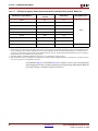
Edge Connector for PCI Express Operation
Edge Connector for PCI Express Operation
Caution! PCI and PCI Express system units provide different DC voltages to the add-in card
connectors. Before plugging the ML555 board into the system unit, the power configuration
header settings must be reviewed to verify that the board will be powered properly. Failure to
configure the power system properly could result in damage to the system unit or the ML555
board. Refer to Figure 3-16, page 78 to see how the SW8 switch and the P18 connector are
configured for PCI Express power.
Figure 3-3 shows the location of the edge connector and power management headers for
PCI Express systems.
SW8
Slide Switch SW8
P13: 8-Lane Connector
for PCI Express Designs
P45:
(Configure for
PCI Express Lane
Width Presence Detect)
P18: (Install Shunts for
PCI Express Designs)
UG201_c3_03_022708
Figure 3-3:
Virtex-5 FPGA ML555 Development Kit
UG201 (v1.4) March 10, 2008
Connector and Power Management Headers for PCI Express Designs
www.xilinx.com
23
R
Chapter 3: Hardware Description
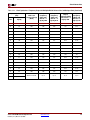
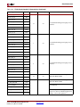
Table 3-1 shows the connector pin assignment for PCI Express designs. The board
supports x1, x4, and x8 endpoint designs. The ML555 board is an endpoint add-in card.
Port names are with respect to the system board host.
Table 3-1:
P13 Edge Connector Socket Pinout for PCI Express Designs
P13 A Side
Signal
P13 B Side
Signal
A1
PCIE_PRSNT1_B(1)
B1
+12 VOLTS
A2
+12 VOLTS
B2
+12 VOLTS
A3
+12 VOLTS
B3
+12 VOLTS
A4
GND
B4
GND
A5
JTAG_TCK(2)
B5
SMCLK(2)
A6
JTAG_TDI(2)
B6
SMDAT(2)
A7
JTAG_TDO(2)
B7
GND
A8
JTAG_TMS(2)
B8
+3.3 VOLTS
A9
+3.3 VOLTS
B9
JTAG_TRST_B(2)
A10
+3.3 VOLTS
B10
+3.3 VOLTSAUX(2)
A11
PCIE_PERST(6)
B11
PCIE_WAKE_B(2)
KEY
24
KEY
A12
GND
B12
RESERVED
A13
PCIE_REFCLKP(3)
B13
GND
A14
PCIE_REFCLKN(3)
B14
PETP0(4)
A15
GND
B15
PETN0(4)
A16
PERP0(5)
B16
GND
A17
PERN0(5)
B17
PCIE_PRSNT2_B(1)
A18
GND
B18
GND
A19
RESERVED
B19
PETP1
A20
GND
B20
PETN1
A21
PERP1
B21
GND
A22
PERN1
B22
GND
A23
GND
B23
PETP2
A24
GND
B24
PETN2
A25
PERP2
B25
GND
A26
PERN2
B26
GND
A27
GND
B27
PETP3
A28
GND
B28
PETN3
A29
PERP3
B29
GND
www.xilinx.com
Virtex-5 FPGA ML555 Development Kit
UG201 (v1.4) March 10, 2008
R
Edge Connector for PCI Express Operation
Table 3-1:
P13 Edge Connector Socket Pinout for PCI Express Designs (Continued)
P13 A Side
Signal
P13 B Side
Signal
A30
PERN3
B30
RESERVED
A31
GND
B31
PCIE_PRSNT2_B(1)
A32
RESERVED
B32
GND
A33
RESERVED
B33
PETP4
A34
GND
B34
PETN4
A35
PERP4
B35
GND
A36
PERN4
B36
GND
A37
GND
B37
PETP5
A38
GND
B38
PETN5
A39
PERP5
B39
GND
A40
PERN5
B40
GND
A41
GND
B41
PETP6
A42
GND
B42
PETN6
A43
PERP6
B43
GND
A44
PERN6
B44
GND
A45
GND
B45
PETP7
A46
GND
B46
PETN7
A47
PERP7
B47
GND
A48
PERN7
B48
PCIE_PRSNT2_B(1)
A49
GND
B49
GND
Notes:
1. PCIE_PRSNT1_B can be connected to one of three PCIE_PRSNT2_B signals by connecting a shunt on
connector P45. See Table 3-2 for application information.
2. No connect on the ML555 board.
3. The ML555 board layout provides two methods of interfacing the PCIE_REFCLK to the FPGA. The
default method is to AC couple the 100 MHz PCIE_REFCLK directly to the GTP_DUAL tile X0Y2
MGTREFCLK input pins. An alternative method is to remove two 0Ω resistors and install an
ICS874003-02 PCI Express Jitter attenuator module, which provides a 100, 125, or 250 MHz reference
clock to the GTP transceiver. The jitter attentuator has two LVDS outputs that connect to the GTP and
FPGA global clock inputs. One of the jitter attentuator LVDS outputs is connected to the MGTREFCLK
inputs of GTP_DUAL tile X0Y2 for PCI Express lanes 0 and 1. The PCIE_REFCLK is also connected to
the FPGA global clock network on pins J16 and J17. Internal FPGA clock buffers distribute this clock to
other GTP_DUAL tiles for PCI Express operation. The architecture of the FPGA permits an external
MGTREFCLK to be driven a maximum of three GTP_DUAL tiles up or down. See “Serial Bus Clocking
with Optional ICS874003-02 Clock Jitter Attenuator (PCI Express Operation),” page 60 for additional
information.
4. The PETPX and PETNX pins connect to the PCI Express transmitter differential pair on the system
board and the PCI Express receiver on the add-in card.
5. The PERPX and PERNX pins connect to the PCI Express receiver differential pair on the system board
and the PCI Express transmitter on the add-in card.
6. PCIE_PERST connects to FPGA pin AE14.
The PCI Express Card Electromechanical Specification requires add-in cards to implement
variable-length edge finger pads and tie PRSNT1_B and PRSNT2_B signals together on the
Virtex-5 FPGA ML555 Development Kit
UG201 (v1.4) March 10, 2008
www.xilinx.com
25
R
Chapter 3: Hardware Description
add-in card. More than one PRSNT2_B pin is defined in the x4, x8, and x16 PCI Express
connectors; these are necessary to support up-plugging of the add-in card. Up-plugging is
defined as plugging a smaller link card into a larger link connector. The ML555 board can
be plugged into x8 or x16 lane link connectors.
Prior to installation in the PCI Express system unit, connector P45 must be configured to
indicate the number of PCI Express lanes used in the design, as shown in Table 3-2.
Table 3-2:
Presence Detect Configuration Header for PCI Express Designs (P45)
Physical Connection at
Connector P13
Number of
Active Lanes in
Design
Shunt Position on Connector P45
1
PRSNT1_B(1)
PRSNT2_B
Install shunt on connector P45 pins 5 - 6
P13-A1
P13-B17
4
Install shunt on connector P45 pins 3 - 4
P13-A1
P13-B31
8
Install shunt on connector P45 pins 1 - 2
P13-A1
P13-B48
Notes:
1. P45 pins 2, 4, and 6 are all connected to PCIE_PRSNT1_B on connector P13 pin A1.
2. See Figure 3-3, page 23 for the location of configuration header P45.
Downshifting is defined as plugging an add-in card into a connector that is not fully routed
for all of the lanes. In general, downshifting is not allowed and is physically prevented. An
exception is the x8 connector, in which the system designer can choose to route only the
first four lanes; a x8 lane card must function as a x4 lane card in this scenario. The ML555
board can be used as either a x4 or a x8 lane card depending upon the user design loaded
into the FPGA.
For development purposes, several companies offer x16 to x1 adapters that permit
plugging multilane add-in cards into single lane PCI Express system unit connectors. The
adapter is not provided with the ML555 development kit.
Table 3-3 shows the correlation between PCI Express signals, P13 add-in card pin, FPGA
pins, and GTP_DUAL tile location assignments.
26
www.xilinx.com
Virtex-5 FPGA ML555 Development Kit
UG201 (v1.4) March 10, 2008
R
Table 3-3:
Edge Connector for PCI Express Operation
PCI Express Signals, Add-in Card Connector Pin, and FPGA Pins per GTP_DUAL Tile
PCI Express Signal Name(1)
Add-in Card Connector
P13 Pin
FPGA Pin(2)
PCIE_REFCLK_P
A13
Y4
PCIE_REFCLK_N
A14
Y3
PETP0
B14
W1
PETN0
B15
Y1
PERP0
A16
V2
PERN0
A17
W2
PETP1
B19
AB1
PETN1
B20
AA1
PERP1
A21
AC2
PERN1
A22
AB2
PETP2
B23
AE1
PETN2
B24
AF1
PERP2
A25
AD2
PERN2
A26
AE2
PETP3
B27
AH1
PETN3
B28
AG1
PERP3
A29
AJ2
PERN3
A30
AH2
PETP4
B33
N1
PETN4
B34
P1
PERP4
A35
M2
PERN4
A36
N2
PETP5
B37
T1
PETN5
B38
R1
PERP5
A39
U2
PERN5
A40
T2
Virtex-5 FPGA ML555 Development Kit
UG201 (v1.4) March 10, 2008
www.xilinx.com
GTP_DUAL Tile(3)
X0Y2
X0Y1
X0Y3
27
R
Chapter 3: Hardware Description
Table 3-3:
PCI Express Signals, Add-in Card Connector Pin, and FPGA Pins per GTP_DUAL Tile
PCI Express Signal Name(1)
Add-in Card Connector
P13 Pin
FPGA Pin(2)
PETP6
B41
AL1
PETN6
B42
AM1
PERP6
A43
AK2
PERN6
A44
AL2
PETP7
B45
AP3
PETN7
B46
AP2
PERP7
A47
AN4
PERN7
A48
AN3
PCIE_PERST
A11
AE14
GTP_DUAL Tile(3)
X0Y0
Not Applicable
Notes:
1. Signal names are with respect to the add-in card connector slot nomenclature. PETPx and PETNx connect to the endpoint port GTP
receiver differential pairs. PERPx and PERNx connect to the endpoint port GTP transmitter differential pairs. Port names at the
connector are with respect to the downstream transmitter and receiver ports. The downstream transmitter/receiver ports connect to
the upstream receiver/transmitter ports, respectively.
2. The PCIE_REFCLK and PERNx differential signals are AC coupled with a 0.1 µF capacitor.
3. Dedicated GTP_DUAL tile assignments are required for 8-lane PCI Express Endpoint interfaces with ES silicon. Production silicon
removes GTP_DUAL tile assignment restrictions.
See XAPP1022 [Ref 5] and XAPP1022 [Ref 6] for examples of how to get started designing
and debugging PCI Express endpoint applications using the Integrated Endpoint Block for
PCI Express designs available in Virtex-5 LXT FPGAs.
28
www.xilinx.com
Virtex-5 FPGA ML555 Development Kit
UG201 (v1.4) March 10, 2008
R
64-bit Edge Connector for PCI Operation
64-bit Edge Connector for PCI Operation
Caution! PCI and PCI Express system units provide different DC voltages to the add-in card
connectors. Before plugging the ML555 board into the system unit, the power configuration
header settings must be reviewed to verify that the board will be powered properly. Failure to
configure the power system properly could result in damage to the system unit or the ML555
board. Refer to Figure 3-16, page 78 to see how the SW8 switch and the P18 connector are
configured for PCI or PCI-X system bus power.
Figure 3-4 shows the PCI bus connector and power management headers. Refer to
Figure 3-16, page 78 to see how the SW8 switch and the P18 connector are configured for
PCI power.
SW8
Slide Switch SW8
P1: PCI Bus
Connector
P9
P8
P7
P18: (Remove Shunts for
PCI and PCI-X Modes)
UG201_c3_04_092706
Notes:
1. SW8 and P18 must be configured for PCI power mode.
Figure 3-4:
Virtex-5 FPGA ML555 Development Kit
UG201 (v1.4) March 10, 2008
PCI Connector and Power Management Headers
www.xilinx.com
29
R
Chapter 3: Hardware Description
Table 3-4 shows the edge connector (P1) pin assignment. The component side of the PCB is
side A, and the non-component side or the back of the PCB is side B.
Table 3-4:
P1 PCI Edge Connector Pinout
P1 A
Side
Signal
FPGA Pin(1)
FPGA
I/O
P1 B
Side
Signal
FPGA Pin(1)
FPGA
I/O
32-Bit Connector
30
A1
unused
NC(2)
B1
VCC_MINUS12
NC
A2
VCC12
NC
B2
unused
NC
A3
unused
NC
B3
GND
NC
A4
EDGE_JTAG
NC
B4
EDGE_JTAG
NC
A5
VCC5
NC
B5
VCC5
NC
A6
EDGE_INTA_B
J31
Out
B6
VCC5
NC
A7
EDGE_INTC_B
H30
Out
B7
EDGE_INTB_B
G31
Out
A8
VCC5
NC
B8
EDGE_INTD_B
K29
Out
A9
unused
NC
B9
GND
NC
A10
VCC3V3
NC
B10
unused
NC
A11
unused
NC
B11
unused
NC
3.3V KEY
NC
3.3V KEY
NC
3.3V KEY
NC
3.3V KEY
NC
A14
AUXV
NC
B14
unused
NC
A15
EDGE_RST_B
B15
GND
NC
A16
VCC3V3
B16
CLK_FROM_EDGE(3)
A17
EDGE_GNT_B
B17
GND
A18
GND
B18
EDGE_REQ_B
A19
EDGE_PME_B
L30
Out
B19
VCC3V3
A20
EDGE_AD30
L31
In/Out
B20
EDGE_AD31
K31
In/Out
A21
VCC3V3
B21
EDGE_AD29
P31
In/Out
A22
EDGE_AD28
P30
In/Out
B22
GND
A23
EDGE_AD26
N30
In/Out
B23
EDGE_AD27
M31
In/Out
A24
GND
B24
EDGE_AD25
R28
In/Out
A25
EDGE_AD24
R29
In/Out
B25
VCC3V3
A26
EDGE_IDSEL
P29
In
B26
EDGE_CBE3
F33
In/Out
A27
VCC3V3
B27
EDGE_AD23
T31
In/Out
A28
EDGE_AD22
R31
In/Out
B28
GND
A29
EDGE_AD20
T30
In/Out
B29
EDGE_AD21
U30
In/Out
A30
GND
B30
EDGE_AD19
T28
In/Out
A31
EDGE_AD18
B31
VCC3V3
J30
In
NC
N29
In
NC
NC
NC
NC
NC
T29
In/Out
www.xilinx.com
L34, J14
In
NC
M30
Out
NC
NC
NC
NC
NC
Virtex-5 FPGA ML555 Development Kit
UG201 (v1.4) March 10, 2008
R
Table 3-4:
64-bit Edge Connector for PCI Operation
P1 PCI Edge Connector Pinout (Continued)
P1 A
Side
Signal
A32
EDGE_AD16
A33
VCC3V3
A34
EDGE_FRAME_B
A35
GND
A36
EDGE_TRDY_B
A37
GND
A38
EDGE_STOP_B
A39
VCC3V3
A40
FPGA Pin(1)
FPGA
I/O
P1 B
Side
FPGA Pin(1)
FPGA
I/O
U28
In/Out
B32
EDGE_AD17
U27
In/Out
B33
EDGE_CBE2
E34
In/Out
B34
GND
B35
EDGE_IRDY_B
B36
VCC3V3
B37
EDGE_DEVSEL_B
H34
In/Out
B38
EDGE_PCIXCAP
E31
In
NC
B39
unused
unused
NC
B40
EDGE_PERR_B
A41
unused
NC
B41
VCC3V3
A42
GND
NC
B42
EDGE_SERR_B
A43
EDGE_PAR
G33
In/Out
B43
VCC3V3
A44
EDGE_AD15
R26
In/Out
B44
EDGE_CBE1
E32
In/Out
A45
VCC3V3
B45
EDGE_AD14
R27
In/Out
A46
EDGE_AD13
U26
In/Out
B46
GND
A47
EDGE_AD11
U25
In/Out
B47
EDGE_AD12
T26
In/Out
A48
GND
B48
EDGE_AD10
T25
In/Out
A49
EDGE_AD9
B49
EDGE_M66EN
L29
In
A50
GND
NC
B50
GND
NC
A51
GND
NC
B51
GND
NC
A52
EDGE_CBE0
B52
EDGE_AD8
A33
In/Out
A53
VCC3V3
B53
EDGE_AD7
B33
In/Out
A54
EDGE_AD6
C33
In/Out
B54
VCC3V3
A55
EDGE_AD4
D32
In/Out
B55
EDGE_AD5
C32
In/Out
A56
GND
B56
EDGE_AD3
C34
In/Out
A57
EDGE_AD2
D34
In/Out
B57
GND
A58
EDGE_AD0
H32
In/Out
B58
EDGE_AD1
A59
VCC3V3
B59
VCC3V3
A60
EDGE_REQ64_B
B60
EDGE_ACK64_B
A61
VCC5
NC
B61
VCC5
NC
A62
VCC5
NC
B62
VCC5
NC
NC
B63
unused
NC
B64
GND
NC
NC
F34
In/Out
NC
H33
In/Out
NC
J34
In/Out
NC
NC
B32
In/Out
E33
In/Out
NC
NC
NC
N33
In/Out
Signal
NC
J32
In/Out
NC
NC
K34
In/Out
NC
K33
In/Out
NC
NC
NC
NC
G32
In/Out
NC
K32
In/Out
64-Bit Connector
A63
GND
A64
EDGE_CBE7
L33
Virtex-5 FPGA ML555 Development Kit
UG201 (v1.4) March 10, 2008
In/Out
www.xilinx.com
31
R
Chapter 3: Hardware Description
Table 3-4:
P1 PCI Edge Connector Pinout (Continued)
P1 A
Side
Signal
FPGA Pin(1)
FPGA
I/O
P1 B
Side
FPGA Pin(1)
FPGA
I/O
P34
In/Out
B65
EDGE_CBE6
M32
In/Out
B66
EDGE_CBE4
N34
In/Out
Signal
A65
EDGE_CBE5
A66
VCC3V3
A67
EDGE_PAR64
M33
In/Out
B67
GND
A68
EDGE_AD62
N32
In/Out
B68
EDGE_AD63
P32
In/Out
A69
GND
B69
EDGE_AD61
T33
In/Out
A70
EDGE_AD60
R34
In/Out
B70
VCC3V3
A71
EDGE_AD58
R32
In/Out
B71
EDGE_AD59
R33
In/Out
A72
GND
B72
EDGE_AD57
U33
In/Out
A73
EDGE_AD56
T34
In/Out
B73
GND
A74
EDGE_AD54
U31
In/Out
B74
EDGE_AD55
U32
In/Out
A75
VCC3V3
B75
EDGE_AD53
V32
In/Out
A76
EDGE_AD52
V33
In/Out
B76
GND
A77
EDGE_AD50
V34
In/Out
B77
EDGE_AD51
W34
In/Out
A78
GND
B78
EDGE_AD49
Y33
In/Out
A79
EDGE_AD48
AA33
In/Out
B79
VCC3V3
A80
EDGE_AD46
Y34
In/Out
B80
EDGE_AD47
AA34
In/Out
A81
GND
B81
EDGE_AD45
Y32
In/Out
A82
EDGE_AD44
W32
In/Out
B82
GND
A83
EDGE_AD42
AD34
In/Out
B83
EDGE_AD43
AC34
In/Out
A84
VCC3V3
B84
EDGE_AD41
AC32
In/Out
A85
EDGE_AD40
AB32
In/Out
B85
GND
A86
EDGE_AD38
AB33
In/Out
B86
EDGE_AD39
AC33
In/Out
A87
GND
B87
EDGE_AD37
AF33
In/Out
A88
EDGE_AD36
AE33
In/Out
B88
VCC3V3
A89
EDGE_AD34
AE34
In/Out
B89
EDGE_AD35
AF34
In/Out
A90
GND
B90
EDGE_AD33
AH34
In/Out
A91
EDGE_AD32
B91
GND
NC
A92
unused
NC
B92
unused
NC
A93
GND
NC
B93
unused
NC
A94
unused
NC
B94
GND
NC
NC
NC
NC
NC
NC
NC
NC
NC
NC
AJ34
In/Out
NC
NC
NC
NC
NC
NC
NC
NC
Notes:
1. PCI interface signals are connected to FPGA banks 11, 13, and 15. The reference voltage (VCCO) for these FPGA banks is 3.0V. See the
ML555 board schematics on the CD-ROM for additional information.
2. NC = no connect.
3. PCIBUSCLK1 is routed to FPGA global clock input pin J14, and PCIBUSCLK2 is routed to FPGA regional clock input pin L34. See
“Clock Generation,” page 52 for information on how the PCI bus clock is connected on the ML555 board.
32
www.xilinx.com
Virtex-5 FPGA ML555 Development Kit
UG201 (v1.4) March 10, 2008
R
64-bit Edge Connector for PCI Operation
The PCI bus on the board schematics has signal names of the form EDGE_<signal name>
(denoting the card edge connector signals). The signal names listed in the A Side and B
Side columns of Table 3-4 and Table 3-1, page 24 are standard PCI signal names.
The ML555 board supports both PCI and PCI-X applications. The edge connector
interfaces with the system board connector. Xilinx has LogiCORE solutions available for
both PCI and PCI-X designs to facilitate getting started with the application-specific
design. When installing the ML555 board in a PCI or PCI-X add-in card slot, the PCI
Express bracket must be removed from the ML555 board prior to plugging into the system.
The connectors on the ML555 board are oriented for PCI Express operation. When using a
PCI system, the motherboard should be removed from the system chassis as the I/O on the
ML555 board is not oriented to escape out the back of the system unit frame.
ML555 Configuration Headers for PCI Operation
M66EN - 66 MHz Enable (Connector P9)
P1.B49 is wired to two-pin header pin P9.1. With the P9 jumper shunt removed, M66EN
has a 0.01 μF capacitor to GND. Placing the jumper shunt across pins 1 and 2 of P9 shorts
M66EN to GND.
•
M66EN = GND indicates 0 to 33 MHz operation.
•
M66EN = open indicates 33 MHz to 66 MHz operation. (M66EN is pulled up on the
system board.)
PME# - Power Management Event (Connector P7)
P1.A19 is wired to a two-pin header pin P7.1. PME# is pulled up on the system board. P7.2
is wired to U10 pin L30, allowing the FPGA to drive or sense the PME# signal when a
jumper shunt is placed across pins 1 and 2 of P7. The LogiCORE User Guide for PCI/PCI-X
can be consulted for more information on proper use of PME#. By default the PME# signal
is not connected from the system board to the FPGA, meaning the system boards sees only
the pull-up resistor, and the FPGA input is not connected to the system board signal.
PCIXCAP - PCI-X Capability (Connector P8)
P1.B38 is wired to 3-pin header P8 (center pin), and PCIXCAP is connected to FPGA pin
E31.
•
P8.1 is wired to GND through a 10 KΩ pulldown resistor.
•
P8.2 is wired to P1.B38 and a 0.01μF capacitor to GND.
•
P8.3 is wired to GND.
•
A jumper shunt across P8 pins 1 and 2 indicates that the card is PCI-X 66 capable.
•
No jumper shunt across P8 indicates that the card is PCI-X 133 capable.
•
A jumper shunt across P8 pins 2 and 3 indicates that the card is not PCI-X capable (i.e.,
it is PCI capable and not PCI-X capable).
Reference Designs for PCI and PCI-X Operation
The included FPGA bitstreams are example implementations of the PCI32 v4.1 and PCI-X
v6.1 LogiCORE solutions. In these example implementations, the cores are configured to
provide one PCI I/O Space Base Address Register (BAR) and one Memory Space BAR. The
example application on the user interface in these PCI implementations is the same as
Virtex-5 FPGA ML555 Development Kit
UG201 (v1.4) March 10, 2008
www.xilinx.com
33
R
Chapter 3: Hardware Description
provided with the cores: a simple one-doubleword (DW) register behind the I/O BAR and
a 16 DW memory behind the memory BAR.
To use the provided example implementation for PCI operation:
1.
Load the bitstream onto the ML555 FPGA (see Table 3-37, page 86).
2.
Reboot the host computer (without power cycling the ML555 board).
3.
The host BIOS will configure the core for PCI in the design.
4.
Use a configuration utility to verify that the device was configured properly and look
for a device with a Vendor ID of 0x10EE and a Device ID of 0x0050.
XAPP999 [Ref 7] describes how to build a reference system for the Processor Local Bus
Peripheral Component Interconnect (PLBv46 PCI) core using a MicroBlaze™ processorbased embedded system using the ML555 board.
DDR2 SDRAM SODIMM
The ML555 board contains a 200-pin, small-outline dual in-line memory module
(SODIMM) connector (J2) that supports installation of DDR2 SDRAM SODIMMs of
128 MB, 256 MB, or 512 MB. Dual-rank SODIMMs are not supported. Xilinx provides a
256 MB DDR2-667 SODIMM Micron Semiconductor part number 4HTF3264HY-40E with
the kit. Table 3-5 provides a description of the memory interface signal descriptions,
SODIMM connector pin assignments, and associated FPGA pin assignments. The
SODIMM interface supports customer installation of DDR2-533 and/or DDR2-400
SODIMMs. One of the clock synthesizers must be used to generate the clock frequency for
the SODIMM interface. For most applications, Clock Synthesizer 1 is used for DDR2
memory applications and Clock Synthesizer 2 is used for GTP transceiver applications.
The ML555 board does not support a 72-bit DDR data interface required for parity or error
correction codes (ECC). The speed grade of the FPGA limits the DDR2 memory clock
support to a range of 200-233 MHz or 400-466 million transfers per second. Included on the
CD-ROM is a reference design for the DDR2 memory contained on the ML555. Verilog
source code and a BIT file are included which can be loaded into the FPGA using the
Platform Cable USB download cable and Xilinx iMPACT configuration software. See the
Readme.txt file in the design directory for information about running and implementing
the design.
Characteristics of the DDR2 SDRAM SODIMM (provided with the kit):
•
Organization 32M x 64 bit
•
Memory clock speed 5 ns/200 MHz using the clock synthesizer
•
CAS latency 3 or 4 (DDR2-400)
•
1.8V I/O (Stub-Series Terminated Logic (SSTL_18) compatible)
The data sheet for the DDR2 SDRAM SODIMM kit can be obtained from Micron
Semiconductor at www.micron.com/products/modules. Contact Micron for availability
of other compatible products, including device capacity, clock speeds, and CAS latency
options, in the 200-pin SODIMM form factor.
The ML555 board memory interface design includes on-board 50 Ω termination resistors
to 0.9V, at the FPGA end of the interface, for the 64-bit bidirectional DQ data bus. The
differential DQS signals sourced from the FPGA should use a DIFF_SSTL18_II primitive as
the I/O driver element. The address and control signals have 50 Ω termination resistors to
0.9V at the SODIMM end of the interface. The SODIMM provides a 120 Ω termination
network for the differential clock inputs. On-die termination (ODT) is used to terminate
34
www.xilinx.com
Virtex-5 FPGA ML555 Development Kit
UG201 (v1.4) March 10, 2008
R
DDR2 SDRAM SODIMM
the DQ and DQS ports on the SODIMM side of the interface. The Xilinx Digitally
Controlled Impedance (DCI) standard SSTL18_I_DCI can be utilized to terminate
unidirectional address and control signals transmitted by the FPGA. External 50 Ω
reference resistors are provided to VRN and VRP for the memory interface banks of the
XC5VLX50T FPGA. See the Virtex-5 FPGA User Guide for additional information on DCI.
For assistance designing a DDR2 interface, refer to the Xilinx Memory Corner website at:
www.xilinx.com/products/design_resources/mem_corner/.
For application assistance specifically for Virtex-5 FPGA DDR2 memory controllers, refer
to XAPP858 [Ref 8] and XAPP865 [Ref 9]. Xilinx Memory Interface Generator (MIG) User
Guide [Ref 10] contains detailed technical information for designing memory controllers
using Virtex-5 FPGAs.
Table 3-5:
SDRAM Interface Signal Descriptions
SODIMM
Front
Signal
1
DDR2_VREF
3
GND
5
DQ0
W24
7
DQ1
V24
9
GND
11
DQS0_B
AA31
13
DQS0
AB31
15
GND
17
DQ2
Y26
19
DQ3
W26
21
GND
23
DQ8
V28
25
DQ9
V27
27
GND
29
DQS1_B
AC30
31
DQS1
AB30
33
GND
35
DQ10
W31
37
DQ11
Y31
39
GND
41
GND
43
DQ16
AC29
45
DQ17
AF31
47
GND
49
DQS2_B
SODIMM
Back
Signal
NC(2)
2
GND
NC
4
DQ4
V25
In/Out
In/Out
6
DQ5
W25
In/Out
In/Out
8
GND
10
DM0
In/Out
12
GND
In/Out
14
DQ6
Y27
In/Out
16
DQ7
W27
In/Out
In/Out
18
GND
In/Out
20
DQ12
W29
In/Out
22
DQ13
V29
In/Out
In/Out
24
GND
In/Out
26
DM1
28
GND
In/Out
30
CK0
AH9
Out
In/Out
32
CK0_B
AH10
Out
34
GND
In/Out
36
DQ14
Y28
In/Out
In/Out
38
DQ15
Y29
In/Out
NC
40
GND
NC
NC
42
GND
NC
In/Out
44
DQ20
AF29
In/Out
In/Out
46
DQ21
AF30
In/Out
48
GND
NC
50
No connect
NC
FPGA Pin(1)
FPGA
In/Out
NC
NC
NC
NC
NC
NC
AA30
Virtex-5 FPGA ML555 Development Kit
UG201 (v1.4) March 10, 2008
In/Out
www.xilinx.com
FPGA Pin(1)
FPGA
In/Out
NC
NC
V30
Out
NC
NC
NC
AD30
Out
NC
NC
35
R
Chapter 3: Hardware Description
Table 3-5:
SDRAM Interface Signal Descriptions (Continued)
SODIMM
Front
Signal
FPGA Pin(1)
FPGA
In/Out
SODIMM
Back
Signal
FPGA Pin(1)
FPGA
In/Out
51
DQS2
AA29
In/Out
52
DM2
AH29
Out
53
GND
54
GND
55
DQ18
AJ31
In/Out
56
DQ22
AJ30
In/Out
57
DQ19
AK31
In/Out
58
DQ23
AH30
In/Out
59
GND
60
GND
61
DQ24
AA25
In/Out
62
DQ28
Y24
In/Out
63
DQ25
AA26
In/Out
64
DQ29
AA24
In/Out
65
GND
66
GND
67
DM3
68
DQS3_B
AJ29
In/Out
69
No connect
NC
70
DQS3
AK29
In/Out
71
GND
NC
72
GND
73
DQ26
AB27
In/Out
74
DQ30
AB25
In/Out
75
DQ27
AC27
In/Out
76
DQ31
AB26
In/Out
77
GND
78
GND
NC
79
CKE0
80
No connect
NC
81
DDR2_VCC1V8
NC
82
DDR2_VCC1V8
NC
83
No connect
NC
84
No connect
NC
85
BA2_NC5
86
No connect
NC
87
DDR2_VCC1V8
88
DDR2_VCC1V8
NC
89
A12
AH19
Out
90
A11
AH20
Out
91
A9
AH15
Out
92
A7
AG16
Out
93
A8
AG20
Out
94
A6
AH17
Out
95
DDR2_VCC1V8
96
DDR2_VCC1V8
97
A5
AH22
Out
98
A4
AG22
Out
99
A3
AG17
Out
100
A2
AH18
Out
101
A1
AF18
Out
102
A0
AE18
Out
103
DDR2_VCC1V8
104
DDR2_VCC1V8
105
A10
AG15
Out
106
BA1
AH13
Out
107
BA0
AH14
Out
108
RAS_B
AG13
Out
109
WE_B
AF19
Out
110
S0_B
AG18
Out
111
DDR2_VCC1V8
112
DDR2_VCC1V8
113
CAS_B
114
ODT0
115(3)
No connect
116
No connect
36
NC
NC
NC
AC28
Out
NC
AG8
Out
AF11
Out
NC
NC
NC
NC
AH12
Out
NC
www.xilinx.com
NC
NC
NC
NC
NC
NC
NC
AG30
Out
NC
Virtex-5 FPGA ML555 Development Kit
UG201 (v1.4) March 10, 2008
R
Table 3-5:
DDR2 SDRAM SODIMM
SDRAM Interface Signal Descriptions (Continued)
SODIMM
Front
Signal
SODIMM
Back
Signal
117
DDR2_VCC1V8
NC
118
DDR2_VCC1V8
NC
119
No connect
NC
120
No connect
NC
121
GND
NC
122
GND
NC
123
DQ32
AB28
In/Out
124
DQ36
AK26
In/Out
125
DQ33
AA28
In/Out
126
DQ37
AF28
In/Out
127
GND
128
GND
129
DQS4_B
AK27
In/Out
130
DM4
131
DQS4
AK28
In/Out
132
GND
133
GND
134
DQ38
AE28
In/Out
135
DQ34
AG28
In/Out
136
DQ39
AJ27
In/Out
137
DQ35
AH28
In/Out
138
GND
139
GND
140
DQ44
AC25
In/Out
141
DQ40
AG25
In/Out
142
DQ45
AC24
In/Out
143
DQ41
AG27
In/Out
144
GND
145
GND
146
DQS5_B
AJ26
In/Out
147
DM5
148
DQS5
AH27
In/Out
149
GND
150
GND
151
DQ42
AE27
In/Out
152
DQ46
AD26
In/Out
153
DQ43
AE26
In/Out
154
DQ47
AD25
In/Out
155
GND
156
GND
157
DQ48
AN14
In/Out
158
DQ52
AN13
In/Out
159
DQ49
AP14
In/Out
160
DQ53
AM13
In/Out
161
GND
NC
162
GND
163
No connect
NC
164
CK1
AG10
Out
165
GND
NC
166
CK1_B
AG11
Out
167
DQS6_B
AD11
In/Out
168
GND
169
DQS6
AD10
In/Out
170
DM6
171
GND
172
GND
173
DQ50
AB10
In/Out
174
DQ54
AA8
In/Out
175
DQ51
AA10
In/Out
176
DQ55
AA9
In/Out
177
GND
178
GND
179
DQ56
AC8
In/Out
180
DQ60
AC10
In/Out
181
DQ57
AB8
In/Out
182
DQ61
AC9
In/Out
FPGA Pin(1)
FPGA
In/Out
NC
NC
NC
NC
AD24
Out
NC
NC
NC
NC
Virtex-5 FPGA ML555 Development Kit
UG201 (v1.4) March 10, 2008
www.xilinx.com
FPGA Pin(1)
FPGA
In/Out
NC
AF24
Out
NC
NC
NC
NC
NC
NC
NC
AP12
Out
NC
NC
37
R
Chapter 3: Hardware Description
Table 3-5:
SDRAM Interface Signal Descriptions (Continued)
SODIMM
Front
Signal
183
GND
185
DM7
187
GND
189
DQ58
AM12
191
DQ59
AM11
193
GND
195
SDA
AD9
197
SCL
AE8
199
DDR2_VCC1V8
FPGA Pin(1)
FPGA
In/Out
SODIMM
Back
Signal
184
GND
186
DQS7_B
AJ11
In/Out
188
DQS7
AK11
In/Out
In/Out
190
GND
In/Out
192
DQ62
AK9
In/Out
194
DQ63
AF9
In/Out
In/Out
196
GND
NC
Out
198
GND(SA0)
NC
200
GND(SA1)
NC
NC
AJ9
Out
NC
NC
NC
FPGA Pin(1)
FPGA
In/Out
NC
NC
Notes:
1. DDR2 memory interface signals are connected to FPGA banks 4, 17, 21, and 22. The FPGA reference voltage, VCCO, for these banks
is 1.8V. See the ML555 board schematics on the CD-ROM for further information.
2. NC = no connect.
3. Pin 115 (S1_B) is a no connect because the ML555 board does not support dual-rank SODIMMs.
Power consumption for the DDR2 memory interface is dependent upon the density and
speed of DDR2 memory installed in the SODIMM socket. Table 3-6 shows approximate
1.8V current consumption requirements by density and transfer rate for Micron
Semiconductor SODIMMs supported by the ML555 board. Memory data sheet
specifications should be consulted to determine specific power requirements for the
SODIMM memory devices. Higher densities and higher performance SODIMMs are
supported, however, the user must calculate total application power and stay within the
PCI and/or PCI Express add-in card specifications.
Table 3-6:
DDR2 SODIMM Current Consumption versus Data Transfer Rate
Memory Density
400 MT/s
533 MT/s
667 MT/s
128 MB
480 mA
720 mA
860 mA
256 MB
620 mA
780 mA
940 mA
512 MB
720 mA
780 mA
1100 mA
Current consumption can be higher than shown in Table 3-6 if the four memory banks are
interleaved in the DDR2 memory. Interleaving is accomplished by using the BA[2:0] bank
address as the least-significant column address bits to the DDR2 memory. This increases
power dissipation rather than memory performance, and should be avoided for PCI
Express and PCI bus applications where add-in card power is limited by specification to
25W.
38
www.xilinx.com
Virtex-5 FPGA ML555 Development Kit
UG201 (v1.4) March 10, 2008
R
Small Form-factor Pluggable (SFP) Module Interface
Small Form-factor Pluggable (SFP) Module Interface
The ML555 board has two SFP connectors that support user-installed SFP modules to
support Fibre Channel and Gigabit Ethernet interfaces. The interface is compliant with the
multi-source agreement specification entitled Cooperation Agreement for Small FormFactor Pluggable Transceivers. Table 3-7 lists the connector pins and any associated FPGA
connectivity. The ML555 board provides filtered 3.3V power to both SFP modules per the
SFP specification.
Table 3-7:
SFP Connectors
SFP1-J3
Signal(1)
FPGA Pin(2)
SFP2-J4
FPGA Pin
1
GND
NC(3)
1
NC
2
SFP{1/2}_TX_FAULT(4)
NC
2
NC
3
SFP{1/2}_TX_DISABLE(5)
NC
3
NC
4
IIC_SDA_SFP{1/2}
E8
4
F8
5
II2_SCK_SFP{1/2}
E9
5
F9
6
SFP{1/2}_TCVR_PRESENT_B(6)
NC
6
NC
7
SFP{1/2}_RATE_SEL(7)
NC
7
NC
8
SFP{1/2}_LOS(8)
NC
8
NC
9
GND
NC
9
NC
10
GND
NC
10
NC
11
GND
NC
11
NC
12
SFP{1/2}_RXN
H1
12
J1
13
SFP{1/2}_RXP
G1
13
K1
14
GND
NC
14
NC
15
SFP_RX_3.3V
NC
15
NC
16
SFP_TX_3.3V
NC
16
NC
17
GND
NC
17
NC
18
SFP{1/2}_TXP
F2
18
L2
19
SFP{1/2}_TXN
G2
19
K2
20
GND
NC
20
NC
Notes:
1. Transceiver port names do not include the “{1/2}” shown in this table. Replace “{1/2}” with “SFP1” or “SFP2” as the prefix or suffix
in the port name. The SFP ports are connected to GTP_DUAL tile X0Y4.
2. The I2C interface signals are connected to FPGA bank 20. The reference voltage, VCCO, for this bank is 2.5V.
3. NC = no connect.
4. TX_FAULT input from SFP goes to a board testpoint only.
5. TX_DISABLE has an on-board 4.7 KΩ pull-down resistor. By default, the transceiver is enabled. Some SFP modules require a
stronger pull-down resistor to enable the transmitter. In this situation, resistors R394 and R402 on the ML555 board should be
replaced with a 1 KΩ or lower value resistor to force the transmitter to be enabled.
6. TCVR_PRESENT is not connected to the FPGA.
7. RATE_SEL is pulled up to 3.3V with a 4.7 KΩ resistor. P26 or P29 (pin 1 or 2) is shorted to ground to select a different transmission
rate.
8. Loss of signal from the SFP interface is connected to light emitting diode (LED) D7 for SFP1 and D8 for SFP2.
The ML555 kit does not include SFP modules to plug into the connectors. The user must
provide these.
Virtex-5 FPGA ML555 Development Kit
UG201 (v1.4) March 10, 2008
www.xilinx.com
39
R
Chapter 3: Hardware Description
Serial ATA Interface
The ML555 board provides a single Serial ATA (SATA) disk drive interface connector, J5,
for attachment to an external SATA disk drive. The board supports 1.5 Gbps and 3 Gbps
SATA baud rates. A second SATA interface can be supported using the SMA connectors on
the board and an external SMA to SATA interface board available from Xilinx with part
number HW-AFX-SMA-SATA. The SATA and SMA transceivers are connected to a
common GTP primitive block in the FPGA.
One of the two provided clock synthesizer modules must be used to generate a 150 MHz
reference clock for the SATA GTP transceiver.
The ML555 board does not provide DC power to the drive. An external DC power supply
must provide the drive power. The SATA signal interface cable is not supplied with the
development kit.
Xilinx Alliance Partners have IP cores that can be licensed for development and fielding a
SATA interface solution. The available Alliance Partners IP cores can be found at
www.xilinx.com/alliance/.
XAPP870 [Ref 11] provides a reference design demonstrating how to complete the SATA
physical link initialization between the GTP transceiver in the Virtex-5 LXT FPGA and an
external SATA device.
Table 3-8 lists the signal names and pin assignments for the SATA connector. The ML555
board does not provide DC power for the SATA drives.
Table 3-8:
SATA Connector
J5
Signal
FPGA Pin
1
GND
NC(1)
2
SATA_TXP(2)
B4
3
SATA_TXN(2)
B3
4
GND
NC
5
SATA_RXN(2)
A2
6
SATA_RXP(2)
A3
7
GND
NC
Notes:
1. NC = no connect.
2. The Host side transceiver ports are AC coupled with a 0.01 μF capacitor. The SATA interface is
connected to GTP_DUAL tile X0Y5.
40
www.xilinx.com
Virtex-5 FPGA ML555 Development Kit
UG201 (v1.4) March 10, 2008
R
SMA Connectors
SMA Connectors
The ML555 board has a set of SMA connectors to facilitate routing one set of GTP
transceiver signals off the card to an external device. Another set of SMA connectors is also
provided to input a clock to the GTP MGTREFCLK inputs. There are a number of Xilinx
evaluation boards that convert an SMA interface to SATA, RJ45, or SFP, for example.
GTP_DUAL tile X0Y5 is connected to the SMA connectors.
Table 3-9 lists the signal names and pin assignments for the SMA connectors. SMA
connectors interface to GTP_DUAL tile X0Y5.
Table 3-9:
SMA Connector
SMA Reference
Designator
Signal Name
FPGA Pin
FPGA I/O
J6
SMA_TXP
E2
Out
J7
SMA_TXN
D2
Out
J8
SMA_RXP
D1
In
J9
SMA_RXN
C1
In
J12(1)
SMA_GTPCLK_P4_P
P4
In
J13(1)
SMA_GTPCLK_P3_N
P3
In
Notes:
1. DC blocking capacitors should be installed between the test equipment and the SMA connector when
clocking the GTP transceiver with an external clock source.
Ethernet PHY Daughtercard Support
The ML555 board provides a Xilinx Generic Interface (XGI) connector system wired to
support attachment of the Xilinx Ethernet PHY Daughtercard, part number HW-AFXBERG-EPHY. The EPHY daughtercard is not included with the development kit but can be
purchased separately. The XC5VLX50T FPGA has up to four embedded tri-mode Ethernet
MAC blocks that provide the data link layer interface to the external PHY. The Xilinx
library of soft Ethernet LogiCORE products can also provide Ethernet connectivity
solutions.
The PHY daughtercard contains two Marvell Alaska Gigabit Ethernet over copper
transceivers, part number 88E1111. The PHY devices perform all physical layer functions,
operate at 10/100/1000 Mb/s and support the embedded tri-mode Ethernet MAC within
the Virtex-5 XC5VLX50T FPGA.
The PHY supports GMII, MII, SGMII, and RGMII Ethernet physical interfaces.
The ML555 board contains a 125 MHz oscillator used for the embedded tri-mode EMAC
reference clock.
The ML555 development kit contains two plastic standoffs used with the PHY daughter
card for mechanical support. Refer to UG065 [Ref 3] before powering up the ML555 board
and PHY daughtercard, because the configuration headers on both boards must be set up
properly before power is applied.
Table 3-10 and Table 3-11 list the signal and pin assignments for the J15 and J16 connectors,
respectively.
Virtex-5 FPGA ML555 Development Kit
UG201 (v1.4) March 10, 2008
www.xilinx.com
41
R
Chapter 3: Hardware Description
Table 3-10:
Ethernet PHY Daughtercard J15 Connection(1)
J15-EVEN
Signal
J15-ODD
Signal
FPGA Pin(2)
FPGA In/Out
2
GND
1
P1_TD_TXD1
M8
Out
4
GND
3
P1_TXCTL_TXEN
F11
Out
K8
Out
6
GND
5
P1_TXC_GTXCLK(3)
8
GND
7
P1_COL
L9
In
10
GND
9
P1_TD_TXD3
E12
Out
12
GND
11
P1_TD_TXD2
N9
Out
NC(4)
14
GND
13
No connect
16
GND
15
P1_TD_TXD0
F13
Out
18
GND
17
P1_TXD7
G13
Out
20
GND
19
P1_TXD6
N10
Out
22
GND
21
P1_TXD5
E13
Out
24
GND
23
P1_TXD4
L8
Out
26
GND
25
P1_MDC
E7
Out
28
GND
27
P1_MDIO
U10
In/Out
30
GND
29
P1_TXER
G7
Out
32
GND
31
P1_INT
T11
In
34
GND
33
P0_COL
F6
In
36
GND
35
P0_TXD7
P9
Out
38
GND
37
P0_INT
G5
In
40
GND
39
P0_TXD6
P10
Out
42
GND
41
P0_TXD5
M5
Out
44
GND
43
P0_TXD4
N7
Out
46
GND
45
P0_TD_TXD3
L6
Out
48
GND
47
P0_TD_TXD2
N5
Out
50
GND
49
P0_TD_TXD1
L4
Out
52
GND
51
P0_TD_TXD0
P7
Out
54
GND
53
P0_MDC
K7
Out
56
GND
55
P0_MDIO
R6
In/Out
58
GND
57
RESET_B
T6
Out
60
GND
59
P0_TXC_GTXCLK(3)
T8
Out
62
GND
61
P0_TXCTL_TXEN
U7
Out
64
GND
63
P0_TXER
J7
Out
Notes:
1. UG065 [Ref 3] provides additional information on the HW-AFX-BERG-EPHY Daughtercard.
2. These signals are connected to FPGA banks 12 and 20. The bank reference voltage, VCCO, is 2.5V. See the ML555 board schematics
on the CD-ROM for additional information.
3. These clocks are connected to FPGA clock-capable I/O pins.
4. NC = no connect.
42
www.xilinx.com
Virtex-5 FPGA ML555 Development Kit
UG201 (v1.4) March 10, 2008
R
Table 3-11:
Ethernet PHY Daughtercard Support
Ethernet PHY Daughtercard J16 Connection
FPGA Pin(1)
J16-EVEN
Signal
J16-ODD
Signal
FPGA In/Out
2
GND
1
No connect
4
GND
3
P1_RXC_RXCLK(3)
J10
In
6
GND
5
P1_RD_RXD1
E11
In
8
GND
7
P1_RXCTL_RXDV
M10
In
K18
In
NC(2)
10
GND
9
P1_RCLK1(4)
12
GND
11
P1_CRS
G11
In
14
GND
13
P1_RXER
G12
In
16
GND
15
P1_RXD7
E6
In
18
GND
17
P1_RD_RXD0
T9
In
20
GND
19
No connect
22
GND
21
P1_RD_RXD2
G6
In
24
GND
23
P1_RD_RXD3
T10
In
26
GND
25
P1_RXD4
F5
In
28
GND
27
P1_RXD5
R9
In
30
GND
29
P1_RXD6
H5
In
32
GND
31
P0_CRS
R11
In
34
GND
33
No connect
36
GND
35
P0_RD_RXD0
M6
In
38
GND
37
P0_RD_RXD1
N8
In
40
GND
39
No connect
42
GND
41
P0_RD_RXD2
44
GND
43
No connect
46
GND
45
P0_RXCTL_RXDV
J6
In
48
GND
47
P0_RXD4
P5
In
50
GND
49
P0_RXD5
L5
In
52
GND
51
P0_RXD6
P6
In
54
GND
53
P0_RXD7
K6
In
H14
In
NC
NC
NC
M7
In
NC
56
GND
55
P0_RCLK1(4)
58
GND
57
P0_RD_RXD3
J5
In
60
GND
59
P0_RXER
R8
In
62
GND
61
P0_RXC_RXCLK(3)
H7
In
64
GND
63
No connect
NC
Notes:
1. These signals are connected to FPGA banks 12 and 20. The bank reference voltage, VCCO, is 2.5V. See the ML555 board schematics
on the CD-ROM for additional information.
2. NC = no connect.
3. These clocks are connected to FPGA clock-capable I/O pins.
4. These clocks are connected to FPGA global clock pins.
Virtex-5 FPGA ML555 Development Kit
UG201 (v1.4) March 10, 2008
www.xilinx.com
43
R
Chapter 3: Hardware Description
LVDS Interface
The ML555 board supports low voltage differential signaling (LVDS) applications with 24
transmit channels and 24 receive channels of LVDS signals. Two Samtec QSE-DP
connectors are provided, one for the transmit interface and a second for the receive
interface. Single data rate (SDR) and double data rate (DDR) LVDS applications can be
designed targeting the ML555 board. An SDR SFI-4 interface or XSBI interface consists of
16 LVDS data channels and a forwarded clock. A DDR SPI4.2 like interface consists of 16
LVDS data channels and one forwarded clock. Xilinx has several SDR and DDR LVDS
reference designs that can be ported to run on the ML555 board.
The LVDS transmit and receive connectors can be connected to each other for loopback
testing as shown in Figure 3-6, page 49. The loopback interface cables are not provided
with the kit, but can be ordered separately from Xilinx as part number HW-LVDS-CBL-80.
The LVDS transmit and receive connectors can also be connected to either an ML450 or
ML550 networking interfaces board from Xilinx. Additional information on Xilinx board
products is located at www.xilinx.com/products/devboards/index.htm.
Figure 3-5 shows the P32 and P33 LVDS connectors.
44
www.xilinx.com
Virtex-5 FPGA ML555 Development Kit
UG201 (v1.4) March 10, 2008
R
LVDS Interface
P47: Mezzanine Card Serial Interface
P48: Mezzanine Card 5V
P33: 24-Channel LVDS Interface
P32: 24-Channel LVDS Interface
UG201_c3_05_092706
Figure 3-5:
LVDS and Mezzanine Card Connectors
Table 3-12 and Table 3-13 list the SAMTEC pin connections for P32 and P33, respectively.
Table 3-12:
SAMTEC Pin Connections (P32)
SAMTEC-QSE028-DP P32
Odd
Signal(1)
FPGA
Pin
SAMTEC-QSE028-DP P32
Even
Signal(1)
FPGA
Pin
1
GPIO1_I00_N(2)
K22
2
GPIO1_I01_N(2)
H23
3
GPIO1_I00_P(2)
K23
4
GPIO1_I01_P(2)
G23
5
GND
N/A
6
GND
N/A
7
No connect(3)
N/A
8
No connect
N/A
Virtex-5 FPGA ML555 Development Kit
UG201 (v1.4) March 10, 2008
www.xilinx.com
45
R
Chapter 3: Hardware Description
Table 3-12:
46
SAMTEC Pin Connections (P32) (Continued)
SAMTEC-QSE028-DP P32
Odd
Signal(1)
FPGA
Pin
SAMTEC-QSE028-DP P32
Even
Signal(1)
FPGA
Pin
9
No connect
N/A
10
No connect
N/A
11
GND
N/A
12
GND
N/A
13
GPIO1_I02_N
T24
14
GPIO1_I03_N
N25
15
GPIO1_I02_P
R24
16
GPIO1_I03_P
P25
17
GND
N/A
18
GND
N/A
19
GPIO1_I04_N
P24
20
GPIO1_I05_N
P27
21
GPIO1_I04_P
N24
22
GPIO1_I05_P
P26
23
GND
N/A
24
GND
N/A
25
GPIO1_I06_N
N28
26
GPIO1_I07_N
K26
27
GPIO1_I06_P
M28
28
GPIO1_I07_P
K27
29
GND
N/A
30
GND
N/A
31
GPIO1_I08_N
L28
32
GPIO1_I09_N
M27
33
GPIO1_I08_P
K28
34
GPIO1_I09_P
N27
35
GND
N/A
36
GND
N/A
37
GPIO1_I10_N(4)
E27
38
GPIO1_I11_N(4)
F28
39
GPIO1_I10_P(4)
E26
40
GPIO1_I11_P(4)
E28
41
GPIO1_I12_N(4)
G28
42
GPIO1_I13_N(4)
H27
43
GPIO1_I12_P(4)
H28
44
GPIO1_I13_P(4)
G27
45
GND
N/A
46
GND
N/A
47
GPIO1_I14_N
F26
48
GPIO1_I15_N
H24
49
GPIO1_I14_P
F25
50
GPIO1_I15_P
H25
51
GND
N/A
52
GND
N/A
53
GPIO1_I16_N
G26
54
GPIO1_I17_N
J26
55
GPIO1_I16_P
G25
56
GPIO1_I17_P
J27
57
GND
N/A
58
GND
N/A
59
GPIO1_I18_N
M26
60
GPIO1_I19_N
J25
61
GPIO1_I18_P
M25
62
GPIO1_I19_P
J24
63
GND
N/A
64
GND
N/A
65
GPIO1_I20_N
L26
66
GPIO1_I21_N
L24
67
GPIO1_I20_P
L25
68
GPIO1_I21_P
K24
69
GND
N/A
70
GND
N/A
71
No connect
N/A
72
No connect
N/A
www.xilinx.com
Virtex-5 FPGA ML555 Development Kit
UG201 (v1.4) March 10, 2008
R
LVDS Interface
Table 3-12:
SAMTEC Pin Connections (P32) (Continued)
SAMTEC-QSE028-DP P32
Odd
Signal(1)
FPGA
Pin
SAMTEC-QSE028-DP P32
Even
Signal(1)
FPGA
Pin
73
No connect
N/A
74
No connect
N/A
75
GND
N/A
76
GND
N/A
77
GPIO1_I22_N(2)
K12
78
GPIO1_I23_N(2)
H12
79
GPIO1_I22_P(2)
K13
80
GPIO1_I23_P(2)
J12
Notes:
1. These signals are connected to FPGA banks 1 and 19. The FPGA reference voltage for these banks is
2.5V. See the ML555 board schematics on the CD-ROM for additional information.
2. Bank 1 GPIO clock-capable I/O signals. All others are in FPGA Bank 19.
3. NC = no connect.
4. Bank 19 clock-capable I/O pins.
Table 3-13:
SAMTEC Pin Connections (P33)
SAMTEC-QSE028-DP P33
Odd
Signal(1)
FPGA
Pin
SAMTEC-QSE028-DP P33
Even
Signal(1)
FPGA
Pin
1
GP1O2_I23_P(2)
AF13
2
GP1O2_I22_P(2)
AE13
3
GP1O2_I23_N(2)
AG12
4
GP1O2_I22_N(2)
AE12
5
GND
N/A
6
GND
N/A
7
No Connect
N/A
8
No Connect
N/A
9
No Connect
N/A
10
No Connect
N/A
11
GND
N/A
12
GND
N/A
13
GP1O2_I21_P
AC4
14
GP1O2_I20_P
AB6
15
GP1O2_I21_N
AC5
16
GP1O2_I20_N
AB7
17
GND
N/A
18
GND
N/A
19
GP1O2_I19_P
AA5
20
GP1O2_I18_P
AC7
21
GP1O2_I19_N
AB5
22
GP1O2_I18_N
AD7
23
GND
N/A
24
GND
N/A
25
GP1O2_I17_P
Y8
26
GP1O2_I16_P
AD4
27
GP1O2_I17_N
Y9
28
GP1O2_I16_N
AD5
29
GND
N/A
30
GND
N/A
31
GP1O2_I15_P
AA6
32
GP1O2_I14_P
AD6
33
GP1O2_I15_N
Y7
34
GP1O2_I14_N
AE6
35
GND
N/A
36
GND
N/A
37
GP1O2_I13_P(4)
W6
38
GP1O2_I12_P(4)
AE7
Virtex-5 FPGA ML555 Development Kit
UG201 (v1.4) March 10, 2008
www.xilinx.com
47
R
Chapter 3: Hardware Description
Table 3-13:
SAMTEC Pin Connections (P33) (Continued)
SAMTEC-QSE028-DP P33
Odd
Signal(1)
FPGA
Pin
SAMTEC-QSE028-DP P33
Even
Signal(1)
FPGA
Pin
39
GP1O2_I13_N(4)
Y6
40
GP1O2_I12_N(4)
AF6
41
GP1O2_I11_P(4)
AG5
42
GP1O2_I10_P(4)
W7
43
GP1O2_I11_N(4)
AF5
44
GP1O2_I10_N(4)
V7
45
GND
N/A
46
GND
N/A
47
GP1O2_I09_P
AH5
48
GP1O2_I08_P
Y11
49
GP1O2_I09_N
AG6
50
GP1O2_I08_N
W11
51
GND
N/A
52
GND
N/A
53
GP1O2_I07_P
AH7
54
GP1O2_I06_P
W10
55
GP1O2_I07_N
AG7
56
GP1O2_I06_N
W9
57
GND
N/A
58
GND
N/A
59
GP1O2_I05_P
AJ7
60
GP1O2_I04_P
V8
61
GP1O2_I05_N
AJ6
62
GP1O2_I04_N
U8
63
GND
N/A
64
GND
N/A
65
GP1O2_I03_P
AK7
66
GP1O2_I02_P
V10
67
GP1O2_I03_N
AK6
68
GP1O2_I02_N
V9
69
GND
N/A
70
GND
N/A
71
No Connect
N/A
72
No Connect
N/A
73
No Connect
N/A
74
No Connect
N/A
75
GND
N/A
76
GND
N/A
77
GP1O2_I01_P(2)
AF23
78
GP1O2_I00_P(2)
AE22
79
GP1O2_I01_N(2)
AG23
80
GP1O2_I00_N(2)
AE23
Notes:
1. These signals are connected to FPGA banks 2 and 18. The FPGA reference voltage for these banks is
2.5V. See ML555 board schematics on the CD-ROM for additional information.
2. Bank 2 GPIO clock-capable I/O signals. All others are in FPGA Bank 18.
3. NC = no connect.
4. Bank 18 clock-capable I/O pins.
48
www.xilinx.com
Virtex-5 FPGA ML555 Development Kit
UG201 (v1.4) March 10, 2008
R
LVDS Interface
SAMTEC QSE-028-DP
P32
J12
H12
NC
NC
K24
L24
J24
J25
J27
J26
H25
H24
G27
H27
E28
F28
N27
M27
K27
K26
P26
P27
P25
N25
NC
NC
G23
H23
80
78
76
74
72
70
68
66
64
62
60
58
56
54
52
50
48
46
44
42
P
N
40
38
36
34
32
30
28
26
24
22
20
18
16
14
12
10
8
6
4
2
P
N
P
N
P
N
P
N
P
N
P
N
P
N
P
N
P
N
P
N
P
N
P 79
N 77
75
73
71
69
P 67
N 65
63
P 61
N 59
57
P 55
N 53
51
P 49
N 47
45
P 43
N 41
P 39
N 37
35
P 33
N 31
29
P 27
N 25
23
P 21
N 19
17
P 15
N 13
11
9
7
5
P 3
N 1
SAMTEC QSE-028-DP
P33
K13
K12
AF13
AG12
NC
NC
NC
NC
L25
L26
AC4
AC5
M25
M26
AA5
AB5
G25
G26
Y8
Y9
F25
F26
AA6
Y7
H28
G28
W6
Y6
E26
E27
AG5
AF5
K28
L28
AH5
AG6
M28
N28
AH7
AG7
N24
P24
AJ7
AJ6
R24
T24
AK7
AK6
NC
NC
NC
NC
K23
K22
AF23
AG23
1
3
5
7
9
11
13
15
17
19
21
23
25
27
29
31
33
35
37
39
P
N
41
43
45
47
49
51
53
55
57
59
61
63
65
67
69
71
73
75
77
79
P
N
P
N
P
N
P
N
P
N
P
N
P
N
P
N
P
N
P
N
P
N
P 2
N 4
6
8
10
12
P 14
N 16
18
P 20
N 22
24
P 26
N 28
30
P 32
N 34
36
P 38
N 40
AE13
AE12
P 42
N 44
46
P 48
N 50
52
P 54
N 56
58
P 60
N 62
64
P 66
N 68
70
72
74
76
P 78
N 80
W7
V7
NC
NC
AB6
AB7
AC7
AD7
AD4
AD5
AD6
AE6
AE7
AF6
Y11
W11
W10
W9
V8
U8
V10
V9
NC
NC
AE22
AE23
LVDS Interface Cable Connectivity
(cable not provided in kit)
Clock-Capable I/O in Bank 19 (P32) and Bank 18 (P33)
Clock-Capable I/O in Bank 1 (P32) and Bank 2 (P33)
Ground
UG201_c3_06_092706
Notes:
1. GPIO channel 0 of P32 connects to GPIO channel 0 of P33 when LVDS interface cable connects P32 to
P33.
2. GPIO channel 1 of P32 connects to GPIO channel 1 of P33 when LVDS interface cable connects P32 to
P33.
3. NC = No connection.
Figure 3-6: LVDS Transmit and Receive Connections Between P32 and P33
Virtex-5 FPGA ML555 Development Kit
UG201 (v1.4) March 10, 2008
www.xilinx.com
49
R
Chapter 3: Hardware Description
SAMTEC Mezzanine Expansion Card Support
The ML555 board supports the addition of mezzanine boards attached to connectors P32
and P33. 5V DC power is provided to the mezzanine board on connector P48 (see
Table 3-14). A serial configuration interface is provided on connector P47 (see Table 3-15).
The P47 interface is connected to FPGA Bank 1 with a VCCO reference voltage of 2.5V.
Figure 3-5, page 45 shows the P47 and P48 mezzanine connectors.
Table 3-14:
Connector P48 Pinout
Connector Pin
Signal
Pin 1
+5V
Pin 2
GROUND
Table 3-15:
Connector P47 Pinout
Connector Pin
Signal
FPGA Pin
Pin 1
EXT_SEN
K14
Pin 2
EXT_SDATA
L14
Pin 3
EXT_SCLK
H22
Pin 4
EXT_RESET
G22
Universal Serial Bus Port
The ML555 board provides a connector (P1) for a Universal Serial Bus (USB) port. A USB to
RS-232 converter module is provided on the board. The FPGA connection uses standard
UART interface protocols, while the external interface is USB 2.0. Device drivers are
provided on the reference CD to enable a Microsoft Windows or Linux operating system
personal computer to emulate a serial port.
The board uses the Maxim MAX3008EUP (U4) device to convert the RD, TD, RTS, and CTS
signals from 3.3V (CP2102 side) to 2.5V (FPGA side) of the interface. The MAX3008 RS-232
interface device operates from a 2.5V supply. The interface between the MAX3008 and the
FPGA is at LVCMOS_25 standard levels. The user must provide a UART core internal to
the FPGA to enable serial communication between the FPGA and USB attached serial port.
UART cores are available from the Xilinx IP center at www.xilinx.com/ipcenter.
Table 3-16 describes the RS-232 interface pin assignments.
Table 3-16:
RS-232 Interface Signal Names and Pin Assignments
Signal Name
FPGA In/Out
FPGA Pin Number(1)
Description
USB_RX
Out
USB Receive Data (FPGA UART Transmit port)
K21
USB_TX
In
USB Transmit Data (FPGA UART Receive port)
L20
USB_RTS_B
In
USB Request to Send
L21
USB_CTS_B
Out
USB Clear to Send
J22
USB_DSR_B
Out
USB Data Set Ready
K16
USB_DTR_B
In
USB Data Terminal Ready
L15
50
www.xilinx.com
Virtex-5 FPGA ML555 Development Kit
UG201 (v1.4) March 10, 2008
R
Table 3-16:
Universal Serial Bus Port
RS-232 Interface Signal Names and Pin Assignments (Continued)
Signal Name
FPGA In/Out
USB_RST_B
USB_SUSPEND_B
FPGA Pin Number(1)
Description
In/Out
Active-Low USB Reset (must be held Low for 15 μs to
initiate a reset to the USB controller)
J15
In
USB Suspend (output from USB port driven High when
the USB controller enters the suspend state)
L16
Notes:
1. These signals are connected to FPGA bank 1. The FPGA reference voltage, VCCO, for this bank is 2.5V. See the ML555 board
schematics on the CD-ROM for additional information.
Figure 3-7 is a high-level block diagram of the RS-232 to USB 2.0 interface.
U5
USB_D-
U4
5
USB_VBUS 8
2 1
3 4
J1
GND
3
USB_D+
4
U10
28
USB_DTR_O_B
7
14
USB_DTR_B
L15
27
USB_DSR_I_B
3
18
USB_DSR_B
K16
26
USB_TX_O
8
13
USB_TX
L20
25
USB_RX_I
4
17
USB_RX
K21
24
USB_RTS_O_B
9
12
USB_RTS_B
L21
23
USB_CTS_I_B
5
16
USB_CTS_B
J22
9
USB_RST_I_B
1
20
USB_RST_B
J15
11
USB_SUSPEND_O_B
6
CP2102
Virtex-5
FPGA
15 USB_SUSPEND_B L16
MAX3008
UG201_c3_07_092706
Figure 3-7:
RS-232 Interface Block Diagram
The USB 2.0 cable is not included in the kit. A USB Type A to USB Type B interface cable is
required for ML555 to PC serial communications over the USB interface.
The Platform USB programming cable, included with the Virtex-5 LXT ML555 FPGA
Development Kit for PCI Express, PCI-X, and PCI interfaces, contains a USB Type A to USB
Type B interface cable. If the Platform USB programming cable is not being used to
program devices on the ML555 board, the cable could be used for USB communications
between the ML555 board and a host computer.
USB to UART Bridge
The ML555 board contains a CP2102 USB to UART bridge circuit from Silicon
Laboratories. The USB 2.0 interface is provided external to the board while the FPGA
utilizes a UART interface. The USB interface cable is not provided with the ML555
development kit. USB interface cables are available at many office supply and computer
peripheral consumer stores. A USB B-to-A cable is required to interface a PC USB “A” port
to the ML555 USB “B” port.
Royalty-free Virtual COM Port (VCP) device drivers are provided by Silicon Laboratories
to permit the CP2102 USB to UART bridge to appear as a COM port to the personal
computer (PC) application. The UART interface side of the bridge implements all RS-232
interface signals, including control and handshaking signals. The VCP device driver must
be installed on the PC prior to attempting to establish communications with the ML555
board. The device driver is on the ML555 CD-ROM. The driver allows the PC USB port to
Virtex-5 FPGA ML555 Development Kit
UG201 (v1.4) March 10, 2008
www.xilinx.com
51
R
Chapter 3: Hardware Description
be configured as a serial COM port for the user to continue working with serial
communication utilities like HyperTerminal or Tera Term Pro.
The CP210x USB-to-UART Bridge VCP drivers can be downloaded from the Silicon
Laboratories website at:
http://www.silabs.com/tgwWebApp/public/web_content/products/
Microcontrollers/en/MCU_Downloads.htm
For technical information and support for the CP210x USB-to-UART bridge controller
integrated circuit and the associated VCP device driver, visit the Silicon Laboratories
website at www.silabs.com.
The ML555 FPGA must have a UART design instantiated to communicate with the PC on
the USB interface. A reference design and/or bit image is included on the CD ROM to
permit testing the FPGA to VCP interface. The reference design utilizes the MicroBlaze soft
processor and a UART core to communicate to the PC terminal window.
The ML555 board provides a USB Type-B device port connector that is intended to be
cabled to the host computer with a USB Type-A port connector.
Table 3-17 describes the USB interface pin assignments.
Table 3-17:
USB Connector Signal Names and Pin Assignments
USB
Connector
(J1) Pin
Signal Name
Description
1
VBUS
+5V from HOST system (not used)
2
USB_DATA_N
Bidirectional differential serial data (n-side)
3
USB_DATA_P
Bidirectional differential serial data (p-side)
4
GROUND
Signal ground
Clock Generation
The clock generation section of the ML555 board provides three fixed, two programmable,
and two pairs of differential SMA inputs for clock sources:
1.
Epson EG-2121CA-125.0000M-LHPAB 2.5V LVDS (differential) oscillator
125 MHz FPGA oscillator for Gigabit Ethernet
2.
Epson SG-8002CA-30.0000M-PCC 3.3V LVCMOS (single-ended) oscillator
This clock is buffered via U9. It goes to the CPLD and one of the FPGA global clock
inputs.
3.
Epson EG-2121CA-200.0000M-PHPAB 2.5V LVPECL (differential) oscillator
One pair of SMA clock inputs is connected to the global clock bank, and the other pair of
SMA clock inputs is connected to the GTP_DUAL tile X0Y3 MGTREFCLK inputs. The
global clock SMA ports can also be used as an output port to route internal debug signals
for triggering or viewing on an oscilloscope. Consult the Virtex-5 FPGA User Guide for
additional information on clocking and the appropriate I/O standards for high-speed
clock and data signals.
52
www.xilinx.com
Virtex-5 FPGA ML555 Development Kit
UG201 (v1.4) March 10, 2008
R
Clock Generation
Table 3-18 lists the destination pins of these clock sources. The PCI bus clock goes to a
regional clock input and a global clock input of the FPGA as shown in Table 3-18. The
differential 100 MHz reference clock input for PCI Express designs (PCIE_REFCLK{P/N})
is described in “Serial Bus Clocking with Optional ICS874003-02 Clock Jitter Attenuator
(PCI Express Operation),” page 60. The two clock synthesizer outputs go to GTP REFCLK
inputs as well as global clock inputs.
Table 3-18:
ML555 Board Clock Sources
Clock Designator
Output
Type
Frequency
Destination Pin
Y1
Differential(1)
LVDS
125 MHz
Refer to Figure 3-8.
Y2
Single-Ended
LVCMOS
30 MHz
Clock Buffer U9 input pin 1 (P) then to FPGA U10
Bank 3 L19 (P). See Figure 4-8, page 100 for 30 MHz
clock distribution.
Y3
Differential(1)
LVPECL
200 MHz
FPGA U10 Bank 3 K17 (P) and L18 (N)
P1 pin B16
Single-Ended
PCI 3.3V
33 MHz to
133 MHz
FPGA U10 Bank 3 J14 Global Clock (P)
FPGA U10 Bank 3 Regional Clock input pin L34 (P)
U18 Clock
Synthesizer 1(3)
Differential(1)
LVDS
31.25 MHz to
700 MHz(2)
Refer to Figure 3-8.
U19 Clock
Synthesizer 2(4)
Differential(1)
LVDS
31.25 MHz to
700 MHz(2)
Refer to Figure 3-8.
J10
Differential/
Single-Ended
SMA
Input
User-Specified SMA_GCLKP FPGA U10 Bank 3 Global Clock input
GCLK_P
pin H17 (P)
J11
Differential only
SMA
Input
User-Specified (Must not be connected to a single-ended clock)
GCLK_N
SMA_GCLKN FPGA U10 Bank 3 Global Clock
differential input pin H18 (N)
J12(5)
Differential
SMA
Input
User Specified GTP_DUAL tile X0Y3 MGTREFCLK_P pin P4
J13(5)
Differential
SMA
Input
User Specified GTP_DUAL tile X0Y3 MGTREFCLK_N pin P3
Differential
(system board
input)
LVDS(6)
PCIE_REFCLKP
Virtex-5 FPGA ML555 Development Kit
UG201 (v1.4) March 10, 2008
100 MHz
Spread
Spectrum
FPGA U10 GTP_DUAL tile X0Y2 MGTREFCLK_P
pin Y4 and FPGA U10 global clock input pin J16 as
PCIE_GCLK_P
www.xilinx.com
53
R
Chapter 3: Hardware Description
Table 3-18:
ML555 Board Clock Sources (Continued)
Clock Designator
PCIE_REFCLKN
Output
Type
Frequency
Differential
(system board
input)
LVDS(6)
100 MHz
Spread
Spectrum
Destination Pin
FPGA U10 GTP_DUAL tile X0Y2 MGTREFCLK_N
pin Y3 and FPGA U10 global clock input pin J17
Notes:
1. Differential clock inputs to the FPGA should use the IBUFDS input buffer library primitive. Setting the DIFF_TERM attribute of the
IBUFDS to "TRUE" provides 100 Ω on-chip termination for the LVDS clock source driver.
2. The clock synthesizer has a voltage controller oscillator (VCO) that operates in the 250 to 700 MHz range. The VCO output can be
divided by 1, 2, 4, or 8 to obtain various clock frequencies.
3. Input reference clock frequency for Clock Synthesizer 1 is 10 MHz. The minimum clock adjustment granularity is 10/8 or 1.25 MHz
steps.
4. Input reference clock frequency for Clock Synthesizer 2 is 25 MHz. The minimum clock adjustment granularity is 25/8 or 3.125 MHz
steps.
5. When SMA connectors J12 and J13 are used to provide a source clock to GTP_DUAL tile X0Y3 MGTREFCLK, in-line DC blocking
capacitors should be placed between the test equipment outputs and SMA clock inputs. AC coupling is recommended for GTP clock
inputs. All GTP clock inputs, with the exception of the SMA clock inputs, are AC coupled on the ML555 board assembly.
6. The ML555 board layout provides two methods of interfacing the PCIE_REFCLK to the FPGA. The default method is to AC couple
the 100 MHz PCIE_REFCLK directly to the GTP_DUAL tile X0Y2 MGTREFCLK input pins. An alternative method is to remove two
0Ω resistors and install an ICS874003-02 PCI Express Jitter attenuator module, which provides a 100, 125, or 250 MHz reference clock
to the GTP transceiver. The jitter attentuator has two LVDS outputs that connect to the GTP and FPGA global clock inputs. One of
the jitter attentuator LVDS outputs is connected to the MGTREFCLK inputs of GTP_DUAL tile X0Y2 for PCI Express lanes 0 and 1.
The PCIE_REFCLK is also connected to the FPGA global clock network on pins J16 and J17. Internal FPGA clock buffers distribute
this clock to other GTP_DUAL tiles for PCI Express operation. The architecture of the FPGA permits an external MGTREFCLK to be
driven a maximum of three GTP_DUAL tiles up or down. See “Serial Bus Clocking with Optional ICS874003-02 Clock Jitter
Attenuator (PCI Express Operation),” page 60 for additional information.
54
www.xilinx.com
Virtex-5 FPGA ML555 Development Kit
UG201 (v1.4) March 10, 2008
R
Clock Generation
Figure 3-8 shows a block diagram of the default clock synthesis configuration, provided on
production ML555 boards.
U10 FPGA
L19
FPGA_GCLK_30MHZ
SMA_GCLKP
J10
SMA_GCLKN
J11
P13-A13
P13-A14
10 MHz
25 MHz
J12
J13
125 MHz
H17
H18
DC Block
Capacitors
PCIE_REFCLK
Clock
Synth
#1
0
Clock
Synth
#2
0
1
1
MGT_REFCLKN
H19
H20
GCLKP
GCLKN
MGT_REFCLKP
MGT_REFCLKN
GTP X0Y2
MGT_X0Y0_RCLKP
MGT_X0Y0_RCLKN
AL5
AL4
P4
SMA
P3
Clock
Driver
1
1
2.5V
0
4.7KΩ
Clock
Driver
1
SFP_MGT_REFCLKP
SFP_MGT_REFCLKN
Clock
Mux
Q0
SATA_MGT_GCLKP
SATA_MGT_GCLKN
Q1
SATA_MGT_REFCLKP
SATA_MGT_REFCLKN
G15
G16
H4
H3
J20
J21
E4
D4
Select
SATA_MGT_CLKSEL
200 MHz
LVPECL
P1-B16
Y3
AF4
AF3
SFP_MGT_GCLKP
SFP_MGT_GCLKN
LVPECL_200M_P
LVPECL_200M_N
PCICLK
GCLKN
MGT_REFCLKP
MGT_X0Y1_RCLKP
MGT_X0Y1_RCLKN
0
GCLKP
Y4
SMA
0
GCLK
H15
K17
L18
J14
MGT_REFCLKP
MGT_REFCLKN
MGT_REFCLKP
GTP X0Y1
GTP X0Y0
GTP X0Y3
MGT_REFCLKN
GCLKP
GCLKN
MGT_REFCLKP
MGT_REFCLKN
GTP X0Y4
GCLKP
GCLKN
MGT_REFCLKP
MGT_REFCLKN
GTP X0Y5
Bank 3 I/O
GCLKP
GCLKN
GCLK
UG201_c3_18_022608
Figure 3-8:
Clock Synthesis Block Diagram (Default Configuration)
Virtex-5 FPGA ML555 Development Kit
UG201 (v1.4) March 10, 2008
www.xilinx.com
55
R
Chapter 3: Hardware Description
Figure 3-9 shows an optional clock synthesis configuration, which uses an ICS874003 jitter
attenuator circuit. Contact your local Xilinx representative for more information on this
option.
U10 FPGA
L19
FPGA_GCLK_30MHZ
SMA_GCLKP
J10
SMA_GCLKN
J11
P13-A13
P13-A14
10 MHz
25 MHz
J12
J13
125 MHz
PCIE_REFCLK
Clock
Synth
#1
0
Clock
Synth
#2
0
H17
H18
ICS
874003
1
1
Y4
MGT_REFCLKP
PCIE250M_N
Y3
MGT_REFCLKN
A1
(LVDS)
nA1
PCIE_GCLK_P
J16
PCIE_GCLK_N
J17
GCLKN
H19
H20
GCLKP
GCLKN
MGT_REFCLKP
MGT_REFCLKN
MGT_X0Y1_RCLKP
MGT_X0Y1_RCLKN
AF4
AF3
MGT_X0Y0_RCLKP
MGT_X0Y0_RCLKN
AL5
AL4
SMA
P3
1
1
2.5V
0
4.7KΩ
Clock
Driver
0
SFP_MGT_GCLKP
SFP_MGT_GCLKN
1
SFP_MGT_REFCLKP
SFP_MGT_REFCLKN
Clock
Mux
Q0
SATA_MGT_GCLKP
SATA_MGT_GCLKN
Q1
SATA_MGT_REFCLKP
SATA_MGT_REFCLKN
P1-B16
G15
G16
H4
H3
J20
J21
E4
D4
Select
SATA_MGT_CLKSEL
200 MHz
LVPECL
GCLKN
PCIE250M_P
P4
Clock
Driver
GCLKP
A0
(LVDS)
nA0
SMA
0
GCLK
LVPECL_200M_P
LVPECL_200M_N
PCICLK
H15
K17
L18
J14
GTP X0Y2
GCLKP
MGT_REFCLKP
MGT_REFCLKN
MGT_REFCLKP
GTP X0Y1
GTP X0Y0
GTP X0Y3
MGT_REFCLKN
GCLKP
GCLKN
MGT_REFCLKP
MGT_REFCLKN
GTP X0Y4
GCLKP
GCLKN
MGT_REFCLKP
MGT_REFCLKN
GTP X0Y5
Bank 3 I/O
GCLKP
GCLKN
GCLK
UG201_c3_08_022608
Figure 3-9:
56
Clock Synthesis Block Diagram (Optional Customer Install Configuration)
www.xilinx.com
Virtex-5 FPGA ML555 Development Kit
UG201 (v1.4) March 10, 2008
R
Clock Generation
Global Clock Inputs
Global clock inputs to the FPGA are summarized in Table 3-19. Global clocks are
connected to FPGA bank 3.
Table 3-19:
FPGA Global Clock Inputs
FPGA Pins
Signal Name
Clock Source
L18
LVPECL_200M_N
200 MHz LVPECL oscillator Y3
K17
LVPECL_200M_P
200 MHz LVPECL oscillator Y3
H18
SMA_GCLKN(2,5)
SMA Connector J11
H17
SMA_GCLKP(2,5)
SMA Connector J10(3)
H19
LVDSCLKMOD1_P
Clock Synthesizer 1
H20
LVDSCLKMOD1_N
Clock Synthesizer 1
J20(4)
SATA_MGT_GCLKP
Selectable: 125 MHz Oscillator or Clock Synthesizer 2
J21(4)
SATA_MGT_GCLKN
Selectable: 125 MHz Oscillator or Clock Synthesizer 2
G16
SFP_MGT_GCLKN
125 MHz LVDS Oscillator
G15
SFP_MGT_GCLKP
125 MHz LVDS Oscillator
L19
FPGA_GCLK_30MHZ(3) 30 MHz Oscillator
H14
P0_RCLK1(3)
Port 0 Ethernet PHY Receive Clock (if the EPHY daughtercard is installed)
J19
P1_RCLK1(3)
Port 1 Ethernet PHY Receive Clock (if the EPHY daughtercard is installed)
J14
PCIBUSCLK2(3)
P1-B16 active only when the ML555 board is installed in a PCI bus
connector. Not active when the ML555 board is installed in a PCI Express
connector.
J16(2)
PCIE_GCLK_P
Global clock input available only if an ICS874003-02 PCI Express clock jitter
attenuator circuit is installed on the ML555 board at location U16 (not the
default board configuration). This clock is 100, 125, or 250 MHz as selected
by the CPLD controls. The default is a 250 MHz spread spectrum clock
generated from the add-in card PCI Express input clock on connector P13.
J17(2)
PCIE_GCLK_N
Global clock input available only if an ICS874003-02 PCI Express clock jitter
attenuator circuit is installed on the ML555 board at location U16 (this is not
the default board configuration). This clock is 100, 125, or 250 MHz as
selected by the CPLD controls. The default is a 250 MHz spread spectrum
clock generated from the add-in card input clock for PCI Express operation
on connector P13.
H15(4)
SATA_MGT_CLKSEL
FPGA output used to select the fixed 125 MHz oscillator or the Clock
Synthesizer 2 output to be routed to GTP_DUAL tile X0Y5 MGTREFCLK
and SMA_MGT_GCLK global clock inputs. The ML555 board has a 4.7KΩ
pull-up resistor to 2.5V to provide default selection of clock synthesizer 2 as
the output of the Clock Mux block shown in Figure 3-8 and Figure 3-9.
Virtex-5 FPGA ML555 Development Kit
UG201 (v1.4) March 10, 2008
www.xilinx.com
57
R
Chapter 3: Hardware Description
Table 3-19:
FPGA Global Clock Inputs (Continued)
FPGA Pins
Signal Name
K18, K19, H13 No connects
Clock Source
Unused global clock inputs to FPGA
Notes:
1. AC coupled.
2. The SMA clock input can be differential or single ended. When driven with a single ended clock source, connector J10 should be
used to input the clock to the FPGA. Differential clock inputs to the FPGA should use the IBUFDS input buffer library primitive.
Setting the DIFF_TERM attribute of the IBUFDS to TRUE provides 100 Ω on-chip termination for the LVDS clock source driver.
3. Single-ended clock input. All other clocks are differential inputs.
4. Control output port SATA_MGT_CLKSEL on FPGA pin H15:
(= 0) selects the fixed 125 MHz oscillator output
(= 1) selects the variable-frequency Clock Synthesizer 2 output
as the clock source for the differential global clock inputs on FPGA pins J20 and J21.
5. The SMA GCLK ports can be used as outputs to route internal single-ended or differential signals to an oscilloscope for debugging
ML555 designs.
GTP Reference Clock Inputs
All GTP REFCLK inputs have clock inputs routed to them. Table 3-20 shows GTP location
designators, FPGA pins, and clock sources that drive the reference clock inputs of the GTP
transceivers. The lanes are for PCI Express applications.
Table 3-20:
GTP Reference Clock Inputs
GTP LOC
FPGA Pins(1)
Designator
Signal Name(2)
Clock Source(3,4,5)
Application Usage
X0Y0(6)
AL5, AL4
MGT_X0Y0_REFCLK
Clock Synthesizer 2
Lanes 6 and 7
X0Y1(6)
AF4, AF3
MGT_X0Y1_REFCLK
Clock Synthesizer 1
Lanes 2 and 3
X0Y2(6)
Y4, Y3
PCIE_REFCLK(7)
Spread spectrum clock input from
PCI Express system unit connector
P13. Pins A13 (P) and A14 (N).
Lanes 0 and 1
X0Y3(6)
P4, P3
SMA_GTPCLK
SMA connectors P12 (P) and P13 (N) Lanes 4 and 5
X0Y4
H4, H3
SFP_MGT_REFCLK
125 MHz Oscillator
SFP1 and SFP2 interfaces
X0Y5
E4, D4
SATA_MGT_REFCLK
Selectable: 125 MHz Oscillator or
Clock Synthesizer 2
SATA and SMA interfaces
Notes:
1. GTP REFCLK input pins are listed as differential pairs, MGTREFCLKP and MGTREFCLKN, respectively.
2. Signal names for differential clocking have P/N designators at the end to indicate positive or negative input/output of the
differential clock receiver. See the ML555 board schematics and the ML555 FPGA design constraint file on the CD-ROM for
additional information.
3. The transceivers can still be utilized using internal clock routing resources, either global or GTP clock buffering. See the Virtex-5
FPGA RocketIO GTP Transceiver User Guide for additional information on GTP clocking.
4. Clock Synthesizer 1 is typically utilized to generate the clock for the DDR2 memory.
5. The GTP transceivers can also be clocked using the differential SMA clock inputs, J10 and J11, connected to the global clock inputs.
6. These GTP transceivers are connected to the PCI Express connector J13. The ML555 board supports x1, x4, and x8 lane endpoint PCI
Express applications. ES silicon requires specific GTP_DUAL tile connections for 8-lane PCI Express Endpoint applications.
Production silicon does not have these restrictions.
7. The 100 MHz differential PCI Express system board spread spectrum clock input goes to GTP MGTREFCLK inputs Y4 and Y3. For
multilane PCI Express designs, internal dedicated clock routing resources are used to distribute the PCI Express system clock to
GTP_DUAL tiles X0Y0, X0Y1, and X0Y3. See “Serial Bus Clocking with Optional ICS874003-02 Clock Jitter Attenuator (PCI Express
Operation),” page 60 for additional information.
58
www.xilinx.com
Virtex-5 FPGA ML555 Development Kit
UG201 (v1.4) March 10, 2008
R
Clock Generation
PCI Express applications can utilize the system board’s 100 MHz clock input on the GTP
MGTREFCLK clock input or synthesize a 100 MHz clock using the clock synthesizer, a
DCM, and GTP clocking resources. SATA applications must synthesize a 150 MHz clock
using Clock Synthesizer 2. Gigabit Ethernet applications can use either the 125 MHz
oscillator or a synthesized clock. Fibre channel applications must synthesize either a
53.125 MHz or a 106.25 MHz clock. When using the SFP connectors for Fibre channel and
Gigabit Ethernet, the REFCLK for the SFP must be either Fibre channel or Ethernet speed,
and the SMA connectors should be used to route either the Fibre channel or Ethernet
interface to an offboard connector interface.
The SMA connectors are not AC coupled on the ML555 board, so either internal GTP AC
coupling must be enabled or external AC coupling might be required for interfaces to
offboard transceivers to be electrically compatible.
Parallel Bus Clocking (PCI Operation)
The PCI specification calls for the PCI bus clock, sourced from the motherboard PCI slot, to
have one load on the add-in cards. The LogiCORE solutions for PCI and PCI-X designs,
depending upon bus mode and frequency, require that the PCI bus clock enter the FPGA
on a specific clock pin (refer to Table 1-1).
The ML555 board PCI bus clock is implemented as follows:
•
The PCI bus clock (signal CLK_FROM_EDGE) enters the board on PCI edge
connector P1 pin B16.
•
The clock is then routed in a “Y” topology to two parallel resistors, R2 and R242.
•
The output side of R2 (signal PCIBUSCLK1) is routed to FPGA pin L34 (the regional
clock pin of FPGA).
•
The output side of R242 (signal PCIBUSCLK2) is routed to FPGA pin J14 (the global
clock pin of FPGA).
If full electrical compliance is required, the designer has the option to remove one of the
two resistors (R2 or R242). As shipped, the ML555 board has both resistors installed.
Virtex-5 FPGA ML555 Development Kit
UG201 (v1.4) March 10, 2008
www.xilinx.com
59
R
Chapter 3: Hardware Description
Serial Bus Clocking with Optional ICS874003-02 Clock Jitter Attenuator
(PCI Express Operation)
By default, the ML555 board connects the PCIE_REFCLK input from the add-in card
connector, through two DC blocking capacitors, and then to GTP X0Y2 MGTREFCLK pins
Y4 and Y3.
The ML555 board layout accommodates end-user installation of an ICS874003-02 PCI
Express Clock Jitter attenuator module as shown in Figure 3-10. The ICS device should be
installed in board location U16, and series resistors R450 and R451 need to be removed
from the board assembly. Contact Integrated Devices Technology (IDT) for information
and availability of clock jitter attenuator circuits at www.idt.com.
The PCI Express system clock is an ICS874003-02 clock jitter attenuator circuit. The ICS
device has dual LVDS outputs, one of which is connected to GTP_DUAL tile X0Y2
MGTREFCLK and the other is connected to FPGA global clock input pins J16 and J17. The
jitter attenuator can generate either a 100 MHz or a 250 MHz reference clock for the GTP
transceiver and clock management tile (CMT) within the FPGA.
Figure 3-10 shows the connections from the PCI Express connector to the jitter attenuator
and then to the FPGA. The CPLD image provided with the ML555 board by default selects
a 250 MHz reference clock to be generated by the ICS874003-02. Spare I/O from the FPGA
to CPLD could be used to dynamically select different GTP reference clocks to be
generated by the jitter attentuator circuit. Source code for the CPLD design provided with
the ML555 board is included on the CD-ROM.
Clock Jitter
Attenuator
A0
nA0
PCIE250M_P
PCIE250M_N
A1
nA1
PCIE_GCLK_P
PCIE_GCLK_N
Y4
Y3
J16
J17
MGT_REFCLKP
MGT_REFCLKN
GTP X0Y2
GCLKP
GCLKN
FSEL0
FSEL1
FSEL2
PCIE_REFCLK
MR
P13-A14
OEA
P13-A13
ICS
874003-02
(U16)
U10 FPGA
CPLD_SPARE3
CPLD
CPLD_SPARE2
CPLD_SPARE1
UG201_c3_09_121006
Figure 3-10:
PCI Express Clocking and Control
Spread spectrum clocking is supported by routing the system board clock into the
transceiver and then generating a local clock for the FPGA design. The external clock from
one GTP_DUAL tile can be used to drive the CLKIN ports of neighboring tiles. A
GTP_DUAL tile shares its clock with its neighbors using dedicated internal clock routing
resources. Refer to the Virtex-5 FPGA RocketIO GTP Transceiver User Guide for additional
information on clocking resources.
60
www.xilinx.com
Virtex-5 FPGA ML555 Development Kit
UG201 (v1.4) March 10, 2008
R
Clock Generation
Clock Synthesizers
The ML555 board contains two clock synthesizer circuits that support a wide range of
frequency synthesis capabilities for end-user applications. One of the clock synthesizers
should be used to generate the clock for the DDR2 SODIMM memory. The second clock
synthesizer can be used to generate the reference clock for the GTP transceivers. Two
Integrated Circuit Systems (ICS) ICS8442 Crystal Oscillator to Differential LVDS
Frequency Synthesizer devices are on the board, each with a different crystal oscillator
reference clock.
The ICS8442 device has the following features:
•
Dual differential LVDS outputs
•
Output frequency range: 31.25 MHz to 700 MHz
•
Crystal input frequency range: 10 MHz to 25 MHz
•
VCO operating range: 250 MHz to 700 MHz
•
Parallel or serial interface for programming multiplier and output dividers
•
RMS period jitter: 2.7 ps (typical)
•
Cycle to cycle jitter: 18 ps (typical)
The complete data sheet for the ICS8442 device is available online at
http://www.idt.com/products/getDoc.cfm?docID=6914275
The synthesizer multiplies the reference clock input by a selectable multiplier. The VCO
operates (locks) in a range from 250 to 700 MHz. The VCO output is routed through a
programmable divider to generate the desired output frequency. The supported VCO
frequency divisors are 1, 2, 4, or 8. The resultant clock from the divisor block is then routed
to differential output drivers.
The clock synthesizer can be programmed in either parallel or serial mode. Parallel mode
requires the user to set two DIP switches on the ML555 board, and then press and release a
pushbutton switch to load the desired configuration into the ICS8442. Serial configuration is
accomplished using the FPGA to transmit serial data, clock, and controls to the
synthesizer. A reference design to program the ICS clock synthesizers using the FPGA to
ICS8442 serial configuration interface is provided on the reference CD-ROM included with
the ML555 kit.
The output frequency of the synthesizer is M times the input reference clock frequency,
provided that the internal VCO is locked. An eight-position DIP switch selects the
multiplier value, M. M can be any decimal value from 0 to 511. There are values of M
where the VCO will not obtain frequency lock. The relationship between the input clock
(FXTAL) and the VCO frequency is given by the equation:
FVCO = FXTAL X M
The VCO can be divided by an integer value 1, 2, 4, or 8 using the DIP switches as shown
in Table 3-21.
The frequency output of the clock synthesizer is given by the equation:
FOUT = FVCO/N = FXTAL X M/N (provided the VCO is locked)
Virtex-5 FPGA ML555 Development Kit
UG201 (v1.4) March 10, 2008
www.xilinx.com
61
R
Chapter 3: Hardware Description
Table 3-21:
ICS8442 Divisor Switch Settings
SW12-9 or
SW12-10(2)
“N1”
SW10-9 or
SW12-11(3)
“N0”
Output Divisor
Value
Minimum
Maximum
0
0
1
250
700
0
1
2
125
350
1
0
4
62.5
175
1
1
8
31.25
87.5
Output Frequency (MHz)
Notes:
1. A logic “0” is obtained by moving the switch to the “OPEN” position, and a logic “1” is obtained by
moving the switch to the “CLOSED” position.
2. SW12-9 is for the N1 input of Clock Synthesizer 1, and SW12-10 is for the N1 input of Clock
Synthesizer 2.
3. SW10-9 is for the N0 input of Clock Synthesizer 1, and SW12-11 is for the N0 input of Clock Synthesizer
2.
Parallel Mode Operation
Each clock synthesizer has one set of subminiature DIP switches to set the multiplier and
divider settings in parallel mode. Clock Synthesizer 1, with a 10 MHz reference clock
input, can be set to 0x019 through 0x046, as shown in Table 3-22, page 64. Clock
Synthesizer 2, with a 25 MHz reference clock input, can be set to 0x00A through 0x01C, as
shown in Table 3-23, page 66. DIP switches are provided on the board to allow user
selection of multiplier values that result in valid VCO lock ranges. Multiplier bits that
would result in a VCO unlock condition are hardwired to a logic 0 level on the board.
Figure 3-11 shows the locations of the switches for both synthesizers.
62
www.xilinx.com
Virtex-5 FPGA ML555 Development Kit
UG201 (v1.4) March 10, 2008
R
Clock Generation
SW12:
Parallel Load Inputs for ICS2
SW10:
Parallel Load Inputs for ICS1
SW11: Parallel Load ICS2
SW9: Parallel Load ICS1
UG201_c3_10_092706
Figure 3-11:
Clock Synthesizer Switches (Parallel Mode)
Pushbutton switch SW9 is used to parallel-load the multiplier and divisor selections for
Synthesizer 1 (U8), and switch SW11 is used to parallel-load the multiplier and divisor DIP
switch settings into Synthesizer 2 (U7). Clock synthesizer outputs are not guaranteed to be
in a known state after a power-on cycle. To establish a known clock frequency output
using the parallel mode, the switches must be configured to a valid operating range and
then the SW9 and SW11 pushbutton switches must be pressed and released. The clock
synthesizer can also be configured using FPGA outputs. The “Serial Mode Operation”
section provides additional information.
Table 3-22 and Table 3-23 show all possible values that can be generated by the clock
synthesizer circuit. Table 3-22 shows the clock synthesis ranges with a 10 MHz reference
clock input for Clock Synthesizer 1. There are ranges below and above the VCO operating
range, which must never be selected by the user, where the VCO does not lock and an
Virtex-5 FPGA ML555 Development Kit
UG201 (v1.4) March 10, 2008
www.xilinx.com
63
R
Chapter 3: Hardware Description
output clock is not deterministic. Only one output frequency can be generated based upon
the divisor selection.
Table 3-22:
Clock Synthesizer 1 Frequency Output for Multiplier/Divider Values with a 10 MHz Input Clock
Multiplier Input Selection
(hex)
64
Output
Frequency
(MHz) with
Divisor = 1
N[1:0]=00b
Output
Frequency
(MHz) with
Divisor = 2
N[1:0]=01b
Output
Frequency (MHz)
with Divisor = 4
N[1:0]=10b
Output
Frequency
(MHz) with
Divisor = 8
N[1:0]=11b
M8
M[7:0]
VCO Lock
Frequency Range
(MHz)
0
0x00 – 0x18
Will not LOCK
N/A
N/A
N/A
N/A
0
19
250
250
125
62.5
31.25
0
1A
260
260
130
65
32.5
0
1B
270
270
135
67.5
33.75
0
1C
280
280
140
70
35
0
1D
290
290
145
72.5
36.25
0
1E
300
300
150
75
37.5
0
1F
310
310
155
77.5
38.75
0
20
320
320
160
80
40
0
21
330
330
165
82.5
41.25
0
22
340
340
170
85
42.5
0
23
350
350
175
87.5
43.75
0
24
360
360
180
90
45
0
25
370
370
185
92.5
46.25
0
26
380
380
190
95
47.5
0
27
390
390
195
97.5
48.75
0
28
400
400
200
100
50
0
29
410
410
205
102.5
51.25
0
2A
420
420
210
105
52.5
0
2B
430
430
215
107.5
53.75
0
2C
440
440
220
110
55
0
2D
450
450
225
112.5
56.25
0
2E
460
460
230
115
57.5
0
2F
470
470
235
117.5
58.75
0
30
480
480
240
120
60
0
31
490
490
245
122.5
61.25
0
32
500
500
250
125
62.5
0
33
510
510
255
127.5
63.75
0
34
520
520
260
130
65
www.xilinx.com
Virtex-5 FPGA ML555 Development Kit
UG201 (v1.4) March 10, 2008
R
Table 3-22:
Clock Generation
Clock Synthesizer 1 Frequency Output for Multiplier/Divider Values with a 10 MHz Input Clock (Continued)
Multiplier Input Selection
(hex)
Output
Frequency
(MHz) with
Divisor = 1
N[1:0]=00b
Output
Frequency
(MHz) with
Divisor = 2
N[1:0]=01b
Output
Frequency (MHz)
with Divisor = 4
N[1:0]=10b
Output
Frequency
(MHz) with
Divisor = 8
N[1:0]=11b
M8
M[7:0]
VCO Lock
Frequency Range
(MHz)
0
35
530
530
265
132.5
66.25
0
36
540
540
270
135
67.5
0
37
550
550
275
137.5
68.75
0
38
560
560
280
140
70
0
39
570
570
285
142.5
71.25
0
3A
580
580
290
145
72.5
0
3B
590
590
295
147.5
73.75
0
3C
600
600
300
150
75
0
3D
610
610
305
152.5
76.25
0
3E
620
620
310
155
77.5
0
3F
630
630
315
157.5
78.75
0
40
640
640
320
160
80
0
41
650
650
325
162.5
81.25
0
42
660
660
330
165
82.5
0
43
670
670
335
167.5
83.75
0
44
680
680
340
170
85
0
45
690
690
345
172.5
86.25
0
46
700
700
350
175
87.5
0
0x47 – 0xFF
1
0x00 – 0xFF
Will not LOCK
N/A
N/A
N/A
N/A
Virtex-5 FPGA ML555 Development Kit
UG201 (v1.4) March 10, 2008
www.xilinx.com
65
R
Chapter 3: Hardware Description
Table 3-23 shows the clock synthesis ranges possible with different selections of multiplier
M and divisor N inputs to the ICS8442 device with a 25 MHz reference clock input for
Clock Synthesizer 2.
Table 3-23:
Clock Synthesizer 2 Frequency Output for Multiplier/Divider Values with a 25 MHz Input Clock
Multiplier Input
Selection
(hex)
66
Output
VCO Lock
Output Frequency
Frequency (MHz)
Frequency Range (MHz) with Divisor =
with Divisor = 2
(MHz)
1 N[1:0]=00b
N[1:0]=01b
Output
Frequency
(MHz) with
Divisor = 4
N[1:0]=10b
Output
Frequency
(MHz) with
Divisor = 8
N[1:0]=11b
M8
M[7:0]
0
0x00 – 0x09
Will not LOCK
N/A
N/A
N/A
N/A
0
0A
250
250
125
62.5
31.25
0
0B
275
275
137.5
68.75
34.375
0
0C
300
300
150
75
37.5
0
0D
325
325
162.5
81.25
40.625
0
0E
350
350
175
87.5
43.75
0
0F
375
375
187.5
93.75
46.875
0
10
400
400
200
100
50
0
11
425
425
212.5
106.25
53.125
0
12
450
450
225
112.5
56.25
0
13
475
475
237.5
118.75
59.375
0
14
500
500
250
125
62.5
0
15
525
525
262.5
131.25
65.625
0
16
550
550
275
137.5
68.75
0
17
575
575
287.5
143.75
71.875
0
18
600
600
300
150
75
0
19
625
625
312.5
156.25
78.125
0
1A
650
650
325
162.5
81.25
0
1B
675
675
337.5
168.75
84.375
0
1C
700
700
350
175
87.5
0
0x1D – 0xFF
1
0x00 – 0xFF
Will not LOCK
N/A
N/A
N/A
N/A
www.xilinx.com
Virtex-5 FPGA ML555 Development Kit
UG201 (v1.4) March 10, 2008
R
Clock Generation
Table 3-24 shows the board DIP switch settings for the two clock synthesizer circuits and
the switch positions assigned for the M and N constants. When the switch is in the ON
position, a logic “1” is obtained, and in the OFF position, a logic “0” is obtained.
Figure 3-12 shows a graphic representation of the DIP switches and indicates which switch
positions are used for the M and N input values to the clock synthesizers. When the switch
is in the OFF position a logic 0 is selected. When the switch is not in the OFF position, a
logic 1 is selected. ICS1 input N1 is located on SW12 position 8. Figure 3-12 shows two
examples: one with ICS1 generating a 330 MHz clock and the other with ICS2 generating a
150 MHz clock.
Table 3-24:
M and N Constant Values Set Through ML555 DIP Switch Configuration
Switch Position
Synthesizer Circuit 1
Synthesizer Circuit 2
Parallel Load Pushbutton(1)
SW9
SW11
N1
SW12 pins 8-9
SW12 pins 7-10
N0
SW10 pins 8-9
SW12 pins 6-11
M8
Tied to logic 0
Tied to logic 0
M7
Tied to logic 0
Tied to logic 0
M6
SW10 pins 7-10
Tied to logic 0
M5
SW10 pins 6-11
Tied to logic 0
M4
SW10 pins 5-12
SW12 pins 5-12
M3
SW10 pins 4-13
SW12 pins 4-13
M2
SW10 pins 3-14
SW12 pins 3-14
M1
SW10 pins 2-15
SW12 pins 2-15
M0
SW10 pins 1-16
SW12 pins 1-16
Notes:
1. The parallel load pushbutton switch must be pressed and released to perform a parallel load of the
synthesizer. Alternatively, the FPGA PLOAD1 or PLOAD2 output can be asserted and deasserted to
perform a parallel load without having to press and release the pushbutton switch associated with the
clock synthesizer.
Virtex-5 FPGA ML555 Development Kit
UG201 (v1.4) March 10, 2008
www.xilinx.com
67
R
Chapter 3: Hardware Description
SW10
Position
1: ICS2 - M0
2: ICS1 - M1
2: ICS2 - M1
4: ICS1 - M3
5: ICS1 - M4
Logic 0 Position
Position
1: ICS1 - M0
3: ICS1 - M2
O
F
F
SW12
3: ICS2 - M2
O
F
F
4: ICS2 - M3
5: ICS2 - M4
6: ICS1 - M5
6: ICS2 - N0
7: ICS1 - M6
7: ICS2 - N1
8: ICS1 - N0
8: ICS1 - N1
Logic 1 Position
Example requests ICS1 330 MHz Clock
with M(8:0) = 0x021 and N(1:0) = 00
Logic 0 Position
Logic 1 Position
Example requests ICS2 150 MHz Clock
with M(8:0) = 0x00C and N(1:0) = 01
UG201_c3_11_092706
Figure 3-12:
Clock Synthesizer Parallel Load Switch Settings
Serial Mode Operation
The FPGA provides interface signals to program each synthesizer in serial mode.
Table 3-25 lists the FPGA outputs and pin assignments that connect directly to the ICS8442
clock synthesizer control inputs. A reference design is provided on the CD to demonstrate
serial programming of the clock synthesizer modules from the FPGA.
Table 3-25:
FPGA Signals for Serial Programming of the Clock Synthesizer Modules
Description
FPGA Pin(1)
FPGA
In/Out
PLOAD_1
ICS8442 parallel load input used to parallel-load the multiplier
and divider switch inputs to the device. A pushbutton switch is
provided on the ML555 board to permit the user to load the
settings into the synthesizer. This signal must be a logic “0” level
for serial mode operation.
AP32
Output
STROBE_1
ICS8442 serial load input used to load serialized multiplier and
divisor constants into the ICS8442. Asserted to perform serial to
parallel loading for user-defined clock synthesis. This signal
should be deasserted during serial data clocking, asserted, and
then deasserted for one clock cycle to complete the serial to
parallel loading of the data into the device.
AN33
Output
SDATA_1
This signal contains the ICS8442 serial data input. The serial
data is provided in the sequence T1, T0, NULL, N1, N0, M8, M7,
M6, M5, M4, M3, M2, M1, and finally M0. The ICS8442 data
sheet provides a serial loading timing diagram and definitions
for serial data bits.
AN34
Output
SCLOCK_1
The ICS8442 serial clock input should only be active during
serial loading of the synthesizer. The clock should be deasserted
at all other times. Data is clocked into the ICS8442 on the rising
edge of the SCLOCK. The ICS8442 data sheet provides a serial
loading timing diagram and definitions for serial data bits.
AM32
Output
Signal
68
www.xilinx.com
Virtex-5 FPGA ML555 Development Kit
UG201 (v1.4) March 10, 2008
R
Table 3-25:
Clock Generation
FPGA Signals for Serial Programming of the Clock Synthesizer Modules (Continued)
Description
FPGA Pin(1)
FPGA
In/Out
Clock Synthesizer 1 clock outputs. See Figure 3-8 for a schematic
representation of the clock network on the ML555 board.
H19
Input
H20
Input
MGT_X0Y1_RCLKP
AF4
Input
MGT_X0Y1_RCLKN
AF3
Input
Signal
LVDSCLKMOD1_P
LVDSCLOCKMOD1_N
PLOAD_2
ICS8442 parallel load input used for parallel loading of
multiplier and divider switch inputs to the device. A
pushbutton switch is provided on the ML555 board to permit
the user to load the settings into the synthesizer. This signal is
asserted to perform a parallel load operation. For serial
configuration of the ICS8442, this signal should always be
deasserted (inactive).
AM33
Output
STROBE_2
ICS8442 serial load input used to load serialized multiplier and
divisor constants into the ICS8442. Asserted to perform serial to
parallel loading for user-defined clock synthesis. This signal
should be deasserted during the serial data clocking, asserted,
and then deasserted for one clock cycle to complete the serial to
parallel loading of the data into the device.
AL34
Output
SDATA_2
This signal contains the ICS8442 serial data input. The serial
data is provided in the sequence T1, T0, NULL, N1, N0, M8, M7,
M6, M5, M4, M3, M2, M1, and finally M0. The ICS8442 data
sheet provides a serial loading timing diagram and definitions
for serial data bits.
AK32
Output
SCLOCK_2
The ICS8442 serial clock input should only be active during
serial loading of the synthesizer. The clock should be deasserted
at all other times. Data is clocked into the ICS8442 on the rising
edge of the SCLOCK. The ICS8442 data sheet provides a serial
loading timing diagram and definitions for serial data bits.
AJ32
Output
LVDSCLKMOD2_P(2)
The Clock Synthesizer 2 clock outputs go through clock
multiplexer U3, which connects to the FPGA global clock and
the GTP REFCLK inputs. See Figure 3-8 for a schematic
representation of the clock network on the ML555 board.
J20, E4
Input
J21, D4
Input
AL5
Input
AL4
Input
LVDSCLKMOD2_N(2)
MGT_X0Y0_RCLKP
MGT_X0Y0_RCLKN
Notes:
1. These FPGA output signals are connected to FPGA bank 13. The reference voltage, VCCO, for this bank is 3.0V. See the ML555 board
schematics on the CD-ROM for additional information. The clock synthesizer clocks are not connected to FPGA bank 13.
2. The LVDSCLKMOD_2 differential clock is connected to a differential clock multiplexer. The output of the multiplexer goes to FPGA
global clock inputs J20(P) and J21(N) and MGT_X0Y5 MGTREFCLK inputs E4 and D4.
Virtex-5 FPGA ML555 Development Kit
UG201 (v1.4) March 10, 2008
www.xilinx.com
69
R
Chapter 3: Hardware Description
Figure 3-13 is a timing diagram showing the serial and parallel programming modes of
operation. The parallel mode has priority over serial mode.
SCLOCK
SDATA
T1
T0
NULL
N1
N0
M8
M7
M6
M2
M1
M0
STROBE
100 ns max.
M,N
SCLOCK
PLOAD
20 ns min.
20 ns min.
SDATA
STROBE
M,N
PLOAD
UG201_c3_12_092706
Figure 3-13:
Serial Configuration Interface Timing
Clock-Capable I/O Pins Associated with Clock Inputs
Some clock-capable input and output pins of the FPGA are connected to clocking sources
on the ML555 board. Table 3-26 summarizes these FPGA clock capable inputs and outputs,
along with their FPGA bank numbers and I/O bank reference voltages.
Table 3-26:
FPGA Clock-Capable I/O Connectivity
Signal Name
PCIBUSCLK1
FPGA_CLK_30MHZ
FPGA Pin FPGA Bank Bank VCCO (Volts)
L34
11
3.0
Regional PCI bus applications
AD32
13
3.0
User defined
18
2.5
User-defined LVDS general-purpose I/O
interface
GPIO2_I10_N
V7
GP1O2_I10_P
W7
GPIO2_I11_N
AF5
GP1O2_I11_P
AG5
GPIO2_I12_N
AF6
GP1O2_I12_P
AE7
GPIO2_I13_N
Y6
GP1O2_I13_P
W6
70
Function
www.xilinx.com
Virtex-5 FPGA ML555 Development Kit
UG201 (v1.4) March 10, 2008
R
Table 3-26:
Clock Generation
FPGA Clock-Capable I/O Connectivity (Continued)
Signal Name
FPGA Pin FPGA Bank Bank VCCO (Volts)
GPIO1_I10_N
E27
GP1O1_I10_P
E26
GPIO1_I11_N
F28
GP1O1_I11_P
E28
GPIO1_I12_N
G28
GP1O1_I12_P
H28
GPIO1_I13_N
H27
GP1O1_I13_P
G27
GPIO1_I00_N
K22
GPIO1_I00_P
K23
GPIO1_I01_N
H23
GP1O1_I01_P
G23
GPIO1_I22_N
K12
GP1O1_I22_P
K13
GPIO1_I23_N
H12
GPIO1_I23_P
J12
GPIO2_I00_N
AE23
GPIO2_I00_P
AE22
GPIO2_I01_N
AG23
GP1O2_I01_P
AF23
GPIO2_I22_N
AE12
GP1O2_I22_P
AE13
GPIO2_I23_N
AG12
GPIO2_I23_P
AF13
P0_RXC_RXCLK
H7
P0_TXC_GTXCLK
T8
P1_TXC_GTXCLK
K8
P1_RXC_RXCLK
J10
CPLD_SPARE1
B12
CPLD_SPARE2
A13
PCIW_EN
C13
RTR
B13
Virtex-5 FPGA ML555 Development Kit
UG201 (v1.4) March 10, 2008
Function
19
2.5
User-defined LVDS general-purpose I/O
interface
1
2.5
User-defined LVDS general-purpose I/O
interface
2
2.5
User-defined LVDS general-purpose I/O
interface
12
2.5
Ethernet PHY clocks from daughtercard
HW-AFX-BERG-EPHY
20
2.5
Ethernet PHY clocks from daughtercard
HW-AFX-BERG-EPHY
User defined
Potential dynamic reconfiguration
request or other user-defined application
using a core for PCI operation
www.xilinx.com
71
R
Chapter 3: Hardware Description
Table 3-26:
FPGA Clock-Capable I/O Connectivity (Continued)
Signal Name
FPGA Pin FPGA Bank Bank VCCO (Volts)
DQS2_B
AA30
DQS2
AA29
DQS1_B
AC30
DQS1
AB30
DQS0_B
AA31
DQS0
AB31
DQS5_B
AJ26
DQS5
AH27
DQS4_B
AK27
DQS4
AK28
DQS3_B
AJ29
DQS3
AK29
DQS7_B
AJ11
DQS7
AK11
DQS6_B
AD11
DQS6
AD10
SCL
Function
17
1.8
DDR2 memory data strobes for data
bytes 2, 1, and 0
21
1.8
DDR2 memory data strobes for data
bytes 5, 4, and 3
22
1.8
DDR2 memory data strobes for data
bytes 7 and 6
AE8
DDR2 SODIMM serial clock for presence
detection synchronization with the SDA
bidirectional data signal
IDELAYCTRL Reference Clock Generation
A 200 MHz reference clock for the IDELAYCTRL block is required if the user application
uses the IOB variable delay elements. The ML555 board provides a dedicated 200 MHz
LVPECL_25 oscillator on the board connected to the global clock inputs as shown in
Table 3-19, page 57. The IDELAYCTRL reference clock can alternately be generated within
the FPGA or using one of the clock synthesizers on the board. There are three methods to
generate the reference clock, depending on application usage:
1.
2.
72
Using a DCM with the DCM CLKFX output:
♦
The ML555 30 MHz clock input is used on GCLK pin L19 as the DCM clock input.
♦
The 125 MHz clock input is used through the U2 clock multiplexer GCLK inputs,
G15(P) and G16(N), as the DCM clock input.
♦
The 125 MHz clock input is used through the clock driver GCLK inputs, J20(P)
and J21(N), as the DCM clock input.
Using an external signal generator and connecting the signal generator outputs, either
single-ended or differential to the ML555 SMA clock inputs J10 (GCLKP H17) and J11
(GCLKN H18). The frequency generator output is set to the desired frequency. A DCM
is not required for this method of generating the IDELAYCTRL reference clock.
www.xilinx.com
Virtex-5 FPGA ML555 Development Kit
UG201 (v1.4) March 10, 2008
R
User LEDs
3.
Using one of the clock synthesizer chips. If using the parallel input mode, SW9 and/or
SW11 must be pressed and released to obtain a known output frequency from the
clock synthesizers after a power-on cycle.
♦
Typically, CLOCK_SYNTH1 is reserved for the DDR2 memory clock generation.
If the DDR2 memory is not used or the clock frequency for the DDR2 memory is
200 MHz, this clock can be used for 200 MHz clock generation. The ML555 board
supports DDR2-400, DDR2-533, and DDR2-667 rates.
♦
CLOCK_SYNTH2 routed through the U3 clock mux goes to GCLK_P J20 and
GCLK_N J21. The SATA_MGT_CLKSEL output port on FPGA pin H15 must be
set to either a logic 1 level to select the Clock Synthesizer 2 as the clock source or a
logic 0 level to select the fixed 125 MHz LVDS clock source as input to the global
clock pins. Depending on which GTP elements are used in the design, the second
clock synthesizer might be available for IDELAYCTRL reference clock.
User LEDs
The ML555 board provides three user LEDs that can be turned ON by driving the LED
signals to Ground. Table 3-27 lists the FPGA pin assignments.
Table 3-27:
User LED Pin Assignments
LED Signal
FPGA Pin Number(1)
(FF1136 Package)
Designation
USER_LED0
USER1 D1
H8
USER_LED1
USER2 D2
G8
USER_LED2
USER3 D3
G10
Notes:
1. These signals are connected to FPGA bank 20. The FPGA reference voltage, VCCO, for this bank is 2.5V.
See the ML555 board schematic on the CD-ROM for additional information.
Configuration INIT and DONE LEDs
The ML555 board provides INIT and DONE indicator LEDs, that are turned ON by the
FPGA during the configuration process. The FPGA INIT pin (N14) drives the INIT LED
(D5) buffer transistor (Q2). The FPGA DONE pin (M15) drives the DONE LED (D6) buffer
transistor (Q1). Table 3-28 lists the FPGA pin assignments.
Table 3-28:
Configuration INIT and DONE LED Pin Assignments
LED
Designation
FPGA Pin Number(1)
(FF1136 Package)
FPGA_INIT
D5 INIT
N14
FPGA_DONE
D6 DONE
M15
Notes:
1. These signals are connected to FPGA configuration bank 0. The FPGA reference voltage for this bank
is 2.5V. See the ML555 board schematics on the CD-ROM for additional information.
Virtex-5 FPGA ML555 Development Kit
UG201 (v1.4) March 10, 2008
www.xilinx.com
73
R
Chapter 3: Hardware Description
User Pushbutton Switches
The ML555 board provides three user pushbutton switches. The switch outputs are pulled
up to 2.5V using 4.7 KΩ resistors on the board. The pushbuttons generate a switch closure
to GND when pressed. Switch contact debounce logic must be implemented inside the
FPGA. Table 3-29 lists the FPGA pin assignments.
Table 3-29:
User Pushbutton Switch Assignments
Pushbutton Switch Signal
Description
FPGA Pin Number(1)
(FF1136 Package)
USER_SW0
USER1 SW1
AF21
USER_SW1
USER2 SW2
AF20
USER_SW2
USER3 SW3
AF14
Notes:
1. These signals are connected to FPGA bank 2. The FPGA reference voltage, VCCO, for this bank is 2.5V.
See the ML555 board schematics on the CD-ROM for additional information.
Pushbutton Program Switch (SW6)
The ML555 board provides a pushbutton program switch for initiating reconfiguration of
the Virtex-5 FPGA. A CPLD image is provided with the ML555 board to enable pressing
and releasing the program pushbutton switch (SW6) to initiate a full FPGA device
configuration cycle while the board is powered on. The CPLD design files and bit image
are on the reference CD included in the kit. Pressing this switch causes the FPGA to clear
its internal configuration memory and then load the currently selected image (via the P3
image select jumper block) from the Platform Flash (U1 and U15). See Table 4-6, page 98
for additional information on P3 selection of stored FPGA bitstream images.
Pushbutton Reset Switch (SW7)
The ML555 board provides a pushbutton switch SW7 for a user-assigned function. This
switch, labelled RESET, is wired to the CPLD U6 pin 18 (general-purpose I/O pin). The
switch output is connected by a 4.7 KΩ pull-up resistor to 2.5V. This pushbutton generates
a switch closure to GND when pressed. Switch contact debounce logic must be
implemented inside the CPLD. There are multiple connections between the CPLD U6 and
the FPGA U10 to transmit SW7 activity.
Power Consumption
The PCI specification outlines the power consumption limitations for PCI add-in boards.
The maximum allowable power consumption across all power rails (+5V, +3.3V, +12V,
-12V) is 25W.
On the PCI connector two signals allow the power demand of a board to be specified.
The PRSNT[1:2]# signals are used by a system board to detect if an add-in card is
physically present in the slot and the total power requirements of the add-in card. The
signals are required for the add-in card but are optional for the system board. The ML555
board uses the EDGE_PRSNT1# and EDGE_PRSNT2# signals to request the maximum
25W power limit by grounding PRSNT1# and leaving PRSNT2# open. The
SKT_PRSNT[1:2]# signals on the PCI-X expansion socket (J1) are routed to the FPGA for
sensing.
74
www.xilinx.com
Virtex-5 FPGA ML555 Development Kit
UG201 (v1.4) March 10, 2008
R
Voltage Regulators
Voltage Regulators
The ML555 board is powered from either the PCI slot that it is plugged into, utilizing the
+5V and the +3.3V power rails (see Table 3-4 for the specific power pins within the PCI
edge connector pinout), or the PCI Express slot that it is plugged into utilizing the +3.3V
and +12V power rails.
ML555 DC Power System
The ML555 board plugs into either a parallel PCI bus slot or a serial PCI Express slot in a
system unit. PCI and PCI Express designs use different connector systems for add-in cards.
System units provide unique DC voltages to the add-in cards through the connectors. PCI
system units provide 3.3V and 5V, while PCI Express system units provide 3.3V and 12V to
add-in cards. For PCI Express applications, the ML555 board converts the 12V supply to
5V before powering the onboard voltage regulators. For PCI applications, most of the
onboard regulators are powered by 5V provided by the system units.
The GTP transceiver analog supplies and the FPGA VCCINT voltage are sourced from
either 3.3V from the PCI Express connector or a 5V to 3.0V DC converter on the ML555
board. Two configuration headers are provided on the ML555 board to select between the
5V and 3.3V power sources as indicated in Table 3-30 and Table 3-31. Figure 3-14 is a block
diagram of the ML555 voltage regulator topology.
Virtex-5 FPGA ML555 Development Kit
UG201 (v1.4) March 10, 2008
www.xilinx.com
75
R
Chapter 3: Hardware Description
DDR2_1V8
VR2
AVTTX/RX 1.2V
VR5
AVCCPLL 1.2V
VR6
DDR2_VREF
VR3
GTP
Analog
Power
PCI_VCC (3.0V)
U14
AVCC 1.0V
VR7
PCIe_VCC5
VR1
Jumper = Off
for PCI/PCI-X
Operation
P18
Jumper = On
for PCI
Express
Operation
VCCO_2V5
U13
‘1’
for PCI/PCI-X
Operation
2
1
VCCAUX_2V5
U12
VCCINT_1V0
VR4
‘2’
for PCI
Express
Operation
SW8
3.3V
12V
5V
System Motherboard Slot/Connector
PCI Bus Sources 3.3V and 5V and
PCI Express Sources 3.3V and 12V
UG201_c3_13_022708
Figure 3-14: Voltage Regulator Topology
Caution! The end user must configure the ML555 board prior to installing the board in the
system unit. Failure to configure the board jumpers prior to installation in the system unit might
cause damage to the ML555 board.
76
www.xilinx.com
Virtex-5 FPGA ML555 Development Kit
UG201 (v1.4) March 10, 2008
R
Voltage Regulators
Figure 3-15 shows the location of SW8 and P18 on the ML555 board. The switch and
jumper MUST be configured prior to installing the board in the system unit. SW8 selects
the FPGA VCCINT source (PCI or PCI Express operation), and P18 is the 12V to 5V enable
for PCI Express operation.
SW8: FPGA VCCINT Source Selection
Parallel PCI Bus Mode:
Switch Position “1” towards
PCI Silkscreen on Board
(Slide Switch towards PCI Connector)
Serial PCI Express Mode:
Switch Position “2” towards
PCIe Silkscreen on Board
(Slide Switch away from PCI Connector)
P18: PCI Express 12 V to 5V Enable
Parallel PCI Bus Mode: Open Circuit,
Remove Shunts
Serial PCI Express Mode:
Install Shunts to Connect
P18-1 to P18-2 and P18-3 to P18-4
UG201_c3_14_022708
Figure 3-15:
Virtex-5 FPGA ML555 Development Kit
UG201 (v1.4) March 10, 2008
Location of SW8 and P18
www.xilinx.com
77
R
Chapter 3: Hardware Description
Figure 3-16 shows the jumper settings on SW8 and P18 for Serial PCI Express and Parallel
PCI-X Bus power configurations.
Serial PCI Express Power Configuration
2
Parallel PCI-X Bus Power Configuration
2
1
Connect PCIe
12V to 5V
Converter to
5V Plane
P18
4
Disconnect PCIe
12V to 5V
Converter from
5V Plane
P18
4
3
Slide Switch
3
Slide Switch
PCIe
PCI
1
PCIe
PCI
SW8
SW8
Power FPGA VCCINT
From 3.3V PCI Bus
Power Rail
Power FPGA VCCINT
From Onboard 3.0V
PCI Voltage
Regulator
ML555
Board
ML555
Board
SODIMM
SODIMM
UG201_c3_15_092706
Figure 3-16:
ML555 Power Configuration
Before installing the ML555 board in a system unit, the power system configuration
header, P18, must be checked to ensure that the proper 5V input voltage is selected for the
onboard regulators on the ML555 board according to Table 3-30.
Table 3-30:
ML555 5V Regulator Input Source Selection
ML555 Bus Mode
Application
PCI or PCI-X
Primary Voltage Regulator DC Input Voltage
Source
+5V PCI Connector (System Unit Power)
SW8: 5V Source Selection Header for
Onboard DC Regulators
Open circuit:
• Remove shunts on connector P18 pins 1-2
• Remove shunts on connector P18 pins 3-4
PCI Express
+12V PCI Express Connector (System Unit Power)
Short circuit:
Onboard 12V to 5V DC converter powers most of
the voltage regulators on the ML555 board.
• Connect shunts on connector P18 pins 1-2
• Connect shunts on connector P18 pins 3-4
Shunts are provided on the board.
78
www.xilinx.com
Virtex-5 FPGA ML555 Development Kit
UG201 (v1.4) March 10, 2008
R
Voltage Regulators
The SW8 switch (the source of the 3V power) must be configured according to Table 3-31
to generate GTP transceiver analog and FPGA VCCINT power.
Table 3-31:
VCCINT Voltage Source Selection for PCI or PCI Express Bus Applications
3.3V Power to GTP Analog Supplies
and FPGA VCCINT 1.0V Regulator
Power Source
Voltage Source for FPGA VCCINT
P11: 3V Selection Header Connections
PCI or PCI-X
ML555 on-board 3.0V regulator
power
• Slide SW8 to the OFF position,
connecting pins 2 and 3. Move switch
towards silkscreen on board labeled
PCI. See Figure 3-16 for graphic
illustration.
PCI Express
PCI Express system board 3.3V
power
• Slide SW8 to the ON position,
connecting pins 1 and 2. Move switch
towards silkscreen on board labeled
PCIe. See Figure 3-16 for graphic
illustration.
Caution! Failure to configure SW8 and P18 properly might result in damage to the ML555
onboard +12V to +5V regulator module.
PCI and/or PCI-X Application Add-in Card Power Input
For PCI or PCI-X applications, the host motherboard provides multiple power rails to the
add-in card as shown in Table 3-32. The ML555 board does not use 3.3V AUX, -12V, or
+12V from the system unit in the PCI mode. The PCI Card Electromechanical Specification
places restrictions on the amount of power an add-in card is permitted to consume from
the system unit power supply. An add-in card can consume a maximum of 25 Watts from
all power rails combined. Current values specified in Table 3-32 are maximum supply
currents provided by voltage. An add-in card cannot utilize all maximum capacities and
stay under the 25W maximum specification.
Table 3-32:
PCI and PCI-X Add-in Card Power Rail Capacities
PCI or PCI-X System Unit Power Rail
25W Slot Maximum
+3.3V
7.6A
+3.3V AUX
375 mA
+5V
5.0A
-12V
100 mA
+12V
500 mA
Notes:
1. All values are maximum current permitted per voltage supply. Cards must still stay within 25W
maximum.
Virtex-5 FPGA ML555 Development Kit
UG201 (v1.4) March 10, 2008
www.xilinx.com
79
R
Chapter 3: Hardware Description
Add-in Card DC Power Input (PCI Express Operation)
For PCI Express applications, the ML555 board has +3.3V and +12V power available from
the system unit power supply. The ML555 board does not use the 3.3V AUX power rail.
The PCI Express Card Electromechanical Specification places restrictions on the amount of
power an add-in card can draw from the system unit power supply. The PCI Express
add-in card power consumption limits are shown in Table 3-33.
Single-lane PCI Express applications require the add-in card to power up in the 10W
mode. After the host processor completes configuration, the slot can utilize the full 25W
power allocation. The ML555 board can only plug into a x1 lane PCI Express connector
using an adapter board to convert the eight-lane ML555 PCI Express interface to a singlelane form factor.
The ML555 board plugs into a x8 lane PCI Express slot in a server application with a 25W
power restriction from the system unit. The add-in card slot can be wired for either x4 or x8
lanes, depending on the server. The 75W add-in card slot is primarily for 16-lane PCI
Express applications. The ML555 board can plug into a 16-lane add-in card slot providing
a maximum application link capability of 8 lanes.
Table 3-33:
Add-in Card Power Rail Capacities for PCI Express Operation
Power Rail
10 Watt Slot
25 Watt Slot
75 Watt Slot
Standard Height PCI
Express Card Lanes
x1
x1, x4, or x8 lanes
(server applications)
x16 lanes (supported by the
ML555 board)
+3.3V
3.0A (max)
3.0A (max)
3.0A (max)
+3.3V AUX
375 mA (max)
375 mA (max)
375 mA (max)
+12V
0.5A (max)
2.1A (max)
5.5A (max)
For PCI Express applications, the ML555 board uses the +12V power rail as the input
power to a +12V to +5V DC-to-DC converter. The output of this DC-to-DC converter then
provides the input voltage to most of the voltage regulators on the board. The GTP
transceiver analog supplies and VCCINT are supplied by the 3.3V input from the system
board. For PCI and PCI-X applications, the ML555 board uses the +5V power rail as the
input to all voltage regulators on the board.
The ML555 interface for PCI Express designs supports x1, x4, and x8 lane configurations. A
1 lane to 16 lane converter board for PCI Express designs is required to plug an ML555
board into the x1 slots for PCI Express operation. These interface connectors are available
from Catalyst Enterprises.
ML555 Board DC Power Regulators
The ML555 board contains oncard voltage regulators that provide power for the Virtex-5
FPGA and onboard peripherals (see Table 3-34).
80
www.xilinx.com
Virtex-5 FPGA ML555 Development Kit
UG201 (v1.4) March 10, 2008
R
Table 3-34:
Voltage Regulators
ML555 Onboard DC-to-DC Voltage Converters
ML555 Board
Reference
Designator(1)
VR1(4)
Input Voltage Source
PCI or PCI-X
Mode(2)
Not Used(2)
Nominal
Output
Voltage
PCI Express
Mode(3)
PCI Express
Connector 12V
Input
5V
Maximum
Output
Current
DC Power Sink
6A
Provides 5V power to
onboard voltage
regulators in PCI
Express mode only
VR2(5)
PCI Connector 5V Input
VR1 5V Output
1.8V
6A
DDR2 memory, other
1.8V ML555 peripherals,
and FPGA 1.8V VCCO
reference voltage
VR3(5)
PCI Connector 5V Input
VR1 5V Output
0.9V
6A
DDR2 memory interface
termination and FPGA
0.9V reference voltage
U12(5)
PCI Connector 5V Input
VR1 5V Output
2.5V
5A
FPGA VCCAUX supply
U13(5)
PCI Connector 5V Input
VR1 5V Output
2.5V
5A
FPGA VCCO, XGI
header and other ML555
2.5V peripherals
U14(5)
PCI Connector 5V Input
VR1 5V Output
3.0V
5A
PCI FPGA 3.0V VCCO
reference voltage
VR4(4,5)
PCI Connector 3.3V
Input
U14 3.0V Output
1.0V
6A
VR5(4,5)
PCI Connector 3.3V
Input
PCI Express
Connector 3.3V
Input
1.2V
AVTTTX and
AVTRX
4A
VR6(4,5)
PCI Connector 3.3V
Input
PCI Express
Connector 3.3V
Input
1.2V
AVCCPLL
4A
GTP 1.2V analog
voltage for PLL circuitry
VR7(4,5)
PCI Connector 3.3V
Input
PCI Express
Connector 3.3V
Input
1.0V AVCC
4A
GTP 1.0V analog
voltage
FPGA VCCINT voltage
GTP 1.2V analog
voltage for transmitter
and receiver
termination voltages
Notes:
1. Refer to Figure 3-14, page 76 for a block diagram of the ML555 DC power system. Additional design information is available on the
ML555 board schematics.
2. For PCI and PCI-X design applications, position switch SW8 (Figure 3-16, page 78) to power the GTP transceiver analog supplies
and FPGA VCCINT from the 3.3V input voltage of the PCI connector. Remove shunts on header P18 before applying power to the
ML555 board.
3. For PCI Express design applications, position switch SW8 (Figure 3-16, page 78) to power FPGA VCCINT from the 3.0V regulator
U14 output. GTP transceiver analog supplies are powered from the 3.3V input voltage of the PCI Express connector. Install two
shunts on connector P18 (P18-1 to P18-2 and P18-3 to P18-4) to connect VR1 5V output to power the onboard regulators.
4. These voltage regulator output ports are connected in series through a 10 mΩ Kelvin resistor to the load on the ML555 board. VR1
has a 150 mΩ series Kelvin resistor. Refer to “Power Supply Monitoring,” page 82 for additional information.
5. FPGA power supplies can be turned on in any sequence. The Virtex-5 FPGA data sheet provides a table for “Power-On Current for
Virtex-5 Devices” for a specified voltage power-on sequence (VCCINT - VCCAUX - VCCO). The ML555 board does not have, nor does
it need to have, voltage sequencing circuitry for the DC-to-DC voltage converters on the board.
Virtex-5 FPGA ML555 Development Kit
UG201 (v1.4) March 10, 2008
www.xilinx.com
81
R
Chapter 3: Hardware Description
GTP Transceiver Power
Three low drop-out (LDO) voltage regulators are provided for the analog voltage inputs to
the GTP transceivers. Each regulator has a voltage divider circuit that permits the voltage
to be adjusted, if required, simply by changing resistance value of the voltage divider. Each
regulator can source up to 4A of current. A single voltage regulator sources power to the
AVTTX, AVTRX, and VVTTRXC inputs of the GTP transceivers. The ML555 board does
not provide separate power supplies for the transmitter and receiver termination voltages.
The GTP transceiver analog power supplies are filtered in accordance with the Virtex-5
FPGA RocketIO GTP Transceiver User Guide. Eight of the 12 GTPs on the ML555 board are
specifically targeted solely for PCI Express applications.
DDR2 SODIMM Power
Power consumption for the DDR2 memory interface is dependent upon the density and
speed of the memory installed in the SODIMM socket. Table 3-35 shows approximate 1.8V
current consumption requirements by density and transfer rate for Micron Semiconductor
SODIMMs supported by the ML555 board. Memory data sheet specifications should be
consulted to determine specific power requirements for the SODIMM devices.
Higher densities and higher performance SODIMMs are supported, however, the user
must calculate total application power and stay within the PCI and or PCI Express add-in
card specifications.
Table 3-35:
DDR2 SODIMM Current Consumption versus Data Transfer Rate
Memory Density
400 MT/s
533 MT/s
667 MT/s
128 MB
480 mA
720 mA
860 mA
256 MB
620 mA
780 mA
940 mA
512 MB
720 mA
780 mA
1100 mA
Current consumption can be even higher than shown in Table 3-35 if the four memory
banks are interleaved in the DDR2 memory. Interleaving is accomplished by using the
BA[2:0] bank address as the least-significant column address bits to the DDR2 memory.
While interleaving does not increase memory performance, it increases power dissipation
and should be avoided for PCI Express and PCI bus applications where add-in card power
is limited by specification to 25W.
Power Supply Monitoring
The ML555 board provides capabilities to monitor and measure the voltage and current for
the FPGA internal voltage and all analog GTP voltage regulators. Figure 3-17 shows a
block diagram of the voltage sensing circuit. Only those supplies central to PCI Express
power functions are provided with power supply monitoring capabilities. A 10 mΩ Kelvin
resistor is placed in series between the regulated output and the load on the board. The
input and output port of the series resistor is routed to a header that can be connected to a
Volt-Ohm-Meter (VOM) to measure the voltage drop across the resistor. The current then
can be calculated dividing the voltage by 0.010Ω. Power equals voltage times current.
82
www.xilinx.com
Virtex-5 FPGA ML555 Development Kit
UG201 (v1.4) March 10, 2008
R
Voltage Regulators
VIN
In
VOUT
Voltage
Out
Regulator
Kelvin
Resistor
To Load on ML555
SENSESENSE+
2
1
Voltage
Measurement
Test Points
UG201_c3_16_092706
Figure 3-17:
Voltage Measurement Test Points
The ML555 board provides headers that can be used to monitor the three GTP transceiver
analog power supplies as well as the internal FPGA voltage VCCINT. For PCI Express
applications, power sensing is provided on the output of the +12V to +5V power regulator,
so a total 5V power consumption for the PCI Express application can be determined. The
Kelvin resistor for the 5V power sense point uses a 150 mΩ resistor value instead of the
10 mΩ resistor used in other sense circuits. Current is calculated by dividing the sense
voltage by 0.150Ω.
Figure 3-18 shows the power measurement headers, and Table 3-36 defines their
functions.
Virtex-5 FPGA ML555 Development Kit
UG201 (v1.4) March 10, 2008
www.xilinx.com
83
R
Chapter 3: Hardware Description
P43
P42
P44
P41
P19
UG201_c3_17_091706
Figure 3-18:
Table 3-36:
ML555 Voltage Sensing Power Measurement Headers
Voltage Name
Description
Header Pin Header Pin
Series
(SENSE+)
(SENSE-) Resistance
AVTTX
1.2V GTP Analog Termination Voltage
P41-1
P41-2
10 mΩ
AVCCPLL
1.2V GTP Analog PLL Supply Voltage
P42-1
P42-2
10 mΩ
AVCC
1.0V GTP Analog Supply Voltage
P43-1
P43-2
10 mΩ
VCCINT
1.0V FPGA Internal Voltage
P44-1
P44-2
10 mΩ
5V Power Consumption in PCI Express
Applications. Includes all 5V power
loads.
P19-1
P19-2
150 mΩ
12V-to-5V Converter for
PCI Express Applications
84
Power Measurement Headers
www.xilinx.com
Virtex-5 FPGA ML555 Development Kit
UG201 (v1.4) March 10, 2008
R
XC2C32 CoolRunner-II CPLD U6
The ML555 board cannot margin any of the oncard power supplies. Other Xilinx boards
have power supply monitoring and margining capabilities for application-specific
functions, such as memory interfaces and LVDS interfaces. Characterization boards are
available for GTP transceiver characterization.
ML555 Board Physical Dimensions
The physical height of the ML555 board prevents the system unit covers from being used.
The ML555 board should only be used in a development environment. The ML555 board is
4.7 inches high by 10.5 inches long.
XC2C32 CoolRunner-II CPLD U6
This CPLD supports static or dynamic reconfiguration of the FPGA design image. A
default design image for the CPLD is provided with the ML555 board to support static
reconfiguration. To select one of four designs, the user configures the P3 configuration
image select header and then either powers up the board, or depresses and releases the
PROG switch while the board is in a system unit. The design image might require the
board to be plugged into either a parallel PCI bus system board slot or a serial PCI Express
system board slot.
Figure 4-5, page 92 and Table 4-4, page 94 summarize the CPLD connections to:
•
U1 and U15: XCF32PFSG48C Platform Flash configuration devices
•
U10: XC5VLX50T FPGA Bank 20
•
U10: XC5VLX50T FPGA Bank 0 Configuration Interface
•
P3: Configuration Image select header
•
SW6 (PROG), SW7: General-purpose pushbutton switches
All XC2C32 I/O are 2.5V, and the XC2C32 VCCINT is 1.8V. Chapter 4, “Configuration,”
includes more details concerning the ML555 board configuration.
Virtex-5 FPGA ML555 Development Kit
UG201 (v1.4) March 10, 2008
www.xilinx.com
85
R
Chapter 3: Hardware Description
XCF32PFS48C Platform Flash U1 and U15
Figure 4-5, page 92 and Table 4-5, page 95 summarize the Platform Flash connections to
the XC5VLX50T FPGA U10 and the XC2C32 CPLD U6.
The XCF32PFS48C VCCO is 2.5V.
The Platform Flash holds up to four configuration images for the XC5VLX50T FPGA, two
images in each device. As shown in Figure 4-5, the configuration image is selected by
applying shorting blocks to header P3. When generating design images for the ML555
board, the BITGEN “compress” option is not required to store four design images in the
Platform Flash device. Table 3-37 shows how to select each one of the four configuration
image files depending upon how shunts are installed on header P3.
Table 3-37:
Platform Flash Image Selection
MAN_AUTO
(P3-5 to P3-6)
SHUNT ON
FLASH_IMAGE1_SEL FLASH_IMAGE0_SEL
(P3-3 to P3-4)
(P3-1 to P3-2)
SHUNT ON
FPGA Configuration Image Selected(1)
SHUNT ON
Configure FPGA with Platform Flash U1 Image
0 (4-lane Virtex-5 LogiCORE Endpoint block for
PCI Express memory completer design)
SHUNT ON
SHUNT ON
SHUNT OFF
Configure FPGA with Platform Flash U1 Image
1 (8-lane Virtex-5 FPGA LogiCORE Endpoint
block for PCI Express memory completer
design)
SHUNT ON
SHUNT OFF
SHUNT ON
Configure FPGA with Platform Flash U15 Image
0 (32-bit, 33 MHz memory reference design for
PCI operation)
SHUNT ON
SHUNT OFF
SHUNT OFF
Configure FPGA with Platform Flash U15 Image
1 (64-bit, 133 MHz memory reference design for
PCI-X operation)
Notes:
1. See XAPP1022 [Ref 5]. This application note demonstrates how to generate an Endpoint Block Plus PIO example design and test the
design function in a PC using a memory endpoint test driver.
In concert with the XC2C32 CPLD, the XCF32PFS48C supports static and dynamic
reconfiguration of the FPGA. Chapter 4, “Configuration,” provides more details
concerning the ML555 board configuration.
86
www.xilinx.com
Virtex-5 FPGA ML555 Development Kit
UG201 (v1.4) March 10, 2008
R
Chapter 4
Configuration
The Virtex-5 FPGA ML555 board includes several options to configure the XC5VLX50T
FPGA, XC2C32 CoolRunner-II CPLD, and the XCF32PF Platform Flash. The basic
configuration modes for the Virtex-5 family are:
•
JTAG mode via Parallel Cable IV, Platform Cable USB, or equivalent
•
Master SelectMAP mode via CPLD and Platform Flash
•
Slave SelectMAP mode via CPLD and Platform Flash
•
Slave Serial mode via CPLD and Platform Flash
•
Master Serial mode via CPLD and Platform Flash
The CPLD and Platform Flash can only be configured via JTAG. The Platform Flash
contains up to four unique bitstreams for programming the FPGA. The unique
combination of the FPGA connected to the Platform Flash through the CPLD allows for
static and dynamic bitstream selection of the FPGA via Slave and Master SelectMAP
modes.
This chapter provides a description of the FPGA configuration circuitry and methods used
on the Virtex-5 FPGA ML555 board. The JTAG chain permits the CPLD and/or the
Platform Flash devices to be bypassed with onboard headers. Figure 4-1 shows the
location of configuration switches, connectors, and devices discussed in this chapter.
Virtex-5 FPGA ML555 Development Kit
UG201 (v1.4) March 10, 2008
www.xilinx.com
87
R
Chapter 4: Configuration
U10: FPGA
SW7: RST
U6: CPLD
U1: Platform Flash
SW5: Mode Switch
P38
P5: JTAG Connector
P39
SW6:PROG
P3
P2
P20
UG201_c4_01_091806
Figure 4-1: Configurable Devices
88
www.xilinx.com
Virtex-5 FPGA ML555 Development Kit
UG201 (v1.4) March 10, 2008
R
Configuration Modes
Configuration Modes
Table 4-1 shows the Virtex-5 FPGA configuration modes along with the correct settings for
the Configuration Mode switch (SW5).
Table 4-1:
Configuration Modes
Mode SW5(2)
Mode(1)
JTAG P5
1
(M0)
2
(M1)
3
(M2)
Master SelectMAP(3)
N/A
0
0
1
Slave SelectMAP(3)
N/A
0
1
1
Yes
1
0
1
Master Serial
N/A
0
0
0
Slave Serial
N/A
1
1
1
JTAG
Notes:
1. Switch position 4 is used to select the DC voltage level applied to the HSWAPEN FPGA configuration
input. This switch controls whether the weak pull-up resistors on the FPGA I/Os are enabled or
disabled prior to configuration.
2. 0 = switch position is Closed or in the ON position. 1 = switch position is Open or in the OFF position.
See Figure 4-2.
3. When using SelectMAP configuration mode, see Table 4-7 for configuration of the CCLK source for
master mode operation. Slave SelectMAP clocking is not supported on the ML555 board. Master
SelectMAP, with a minimum 20 MHz configuration clock (CCLK) frequency, is the recommended
configuration method for PCI, PCI-X, and PCI Express applications utilizing the ML555 board.
Figure 4-2 shows the Configuration Mode switch. SW5 position 4 is used to select the DC
voltage level applied to the HSWAPEN input pin in the FPGA configuration bank. If the
switch is in the OFF position, the weak preconfiguration I/O pull-up resistors are disabled.
If the switch is in the ON position, the weak preconfiguration I/O pull-up resistors are
enabled.
OFF
Logic
0
1 2 3 4
SW5
Logic
1
MODE
UG201_c4_02_091706
Figure 4-2:
Configuration Mode Switch
JTAG Chain
Figure 4-3 shows the JTAG chain on the ML555 board. The chain can be driven by the
following sources:
•
Xilinx Parallel Cable IV or Platform Cable USB
•
Other JTAG cables
The JTAG chain supports bypassing of the CPLD or the Platform Flash devices. The FPGA
cannot be bypassed. Board connector/header P39 is used to enable or bypass the CPLD,
Virtex-5 FPGA ML555 Development Kit
UG201 (v1.4) March 10, 2008
www.xilinx.com
89
R
Chapter 4: Configuration
connector/header P38 is used to enable or bypass the Platform Flash device U1, and
connector/header P20 is used to enable or bypass the second Platform Flash device U15.
To enable the CPLD for JTAG configuration, the shunts on P39 are connected from pin 1 to
pin 2, and a second shunt connects pin 3 to pin 4. To bypass the CPLD, a single shunt is
installed on P39, connected from pin 2 to pin 3.
To enable the Platform Flash devices for JTAG configuration, two shunts are installed on
connectors P38/P20, connecting from pin 1 to pin 2 for the first shunt, and connecting pin
3 and 4 for the second shunt. To bypass the Platform Flash devices, a single shunt on
P38/P20 is connected from pin 2 to pin 3. The default board configuration enables all four
devices in the JTAG scan chain.
P39
P38
P20
4
3
4
3
4
3
2
JTAG
Connector
P5
U10
FPGA
TDI
TMS
TCK
TDO
U6
CPLD
TDI
2
U1
Platform Flash
#1
1
TDI
TDO
TMS
TCK
2
1
U15
Platform Flash
#2
TDI
TDO
1
TDO
TMS
TCK
TMS
TCK
UG201_c4_03_070706
Figure 4-3:
JTAG Chain
JTAG Port
The ML555 board provides a JTAG connector (P5) to configure the FPGA and program
JTAG devices located in the JTAG chain. Figure 4-4 shows the pin assignments for the
JTAG connector. The JTAG cable connects to P5, and the connector on the ML555 board
has a keyed, plastic shroud to ensure that the device programming cable connects
properly.
P5
JTAG
Connector
2.5V
1
2
3
4
TMS
5
6
TCK
7
8
TDO
9
10
11
12
13
14
2 mm
TDI
UG201_c4_04_070306
Figure 4-4: JTAG Cable Hook-up
90
www.xilinx.com
Virtex-5 FPGA ML555 Development Kit
UG201 (v1.4) March 10, 2008
R
SelectMAP Interface
Table 4-2:
P5 JTAG Header Signal Descriptions and Pin Assignments
Signal Name
Description
P5 Pin
Number
FPGA Pin
Number
CPLD Pin
Number
Flash Pin
Number
JTAG_TMS
JTAG TMS to
FPGA/CPLD/Flash
4
AC14
10
E2
JTAG_TCK
JTAG TCK to
FPGA/CPLD/Flash
6
AB15
11
H3
JTAG_TDO
JTAG TDO from Flash
8
N/A
N/A
E6(2)
JTAG_TDI
JTAG TDI to FPGA TDI
10
AC15
N/A
N/A
Notes:
1. This JTAG connectivity assumes that all four devices are in the JTAG configuration chain.
2. The JTAG_TDO connection is made to the second Platform Flash device, U15. The JTAG_TMS and
JTAG_TCK signals are connected to both U1 and U15 Platform Flash devices.
SelectMAP Interface
The SelectMAP interface is connected to the Platform Flash devices indirectly through the
CPLD. For the SelectMAP interface to operate correctly, the CPLD needs to be
programmed (via JTAG) such that the correct connections are made between the FPGA
and the Flash. The CPLD on the ML555 board has a default image programmed into the
device to permit selection of up to four static design images in the two Platform Flash
configuration devices. The source HDL code and CPLD constraint file are located on the
CD-ROM provided with the ML555 kit.
Figure 4-5 is a general schematic for the Flash/CPLD/FPGA SelectMAP Interface.
Table 4-3 through Table 4-5 list the pinouts for the FPGA, CPLD, and Platform Flash,
respectively. The two Platform Flash devices are connected in parallel, with the exception
of the chip-enable inputs. The CPLD has one chip-enable output for each Platform Flash
device.
Virtex-5 FPGA ML555 Development Kit
UG201 (v1.4) March 10, 2008
www.xilinx.com
91
R
Chapter 4: Configuration
U15
U1
Platform
Flash
Platform
Flash
XCF32PF
XCF32PF D[0:7]
To P2
From P2
8
D[7:0]
CE1 (U15)
36
CE (U1)
42
BUSY
41
U6
CPLD
XC2C32
CF
43
OE/RESET
44
CLKOUT
REV_SEL0
39
CLKIN
REV_SEL1
40
2
4
6
Flash_Image1_Select
MAN_AUTO_B
P3
PB_SW_h
Prog_SW_b
Flash_Image0_Select
1
3
5
31
FORCE(1)
29
WIDE(1)
33
PCIW_EN(1)
32
RTR(1)
5
DONE
6
DOUT_BUSY
34
RDWR_B
23
CS_B
28
PROG_B
27
INIT_B
8
12 8 2 3 13
U10
FPGA
XC5VLX50T
CPLD_SPARE[1:8]
1
CCLK M0 M1 M2 HSWAPEN
30 MHz From/To P2
CPLD CLK
SW5
1
2
3
4
DIP SW
UG201_c4_05_022608
Notes:
1. FORCE, WIDE, PCIW_EN, and RTR are FPGA general-purpose I/Os.
Figure 4-5:
Table 4-3:
Pin
Number
Schematic of Flash/CPLD/FPGA SelectMAP Interface
FPGA Configuration Pin Listing(1)
Net Name
Direction
Pin Type
I/O
CCLK
Description
N15
FPGA_CCLK
N23
FPGA_RDWR_B
I
RDWR_B
Active-Low Read Write
N22
FPGA_CS_B
I
CS_B
Active-Low Chip Select
AD21
MODE0
I
M0
Mode Select 0
AC22
MODE1
I
M1
Mode Select 1
AD22
MODE2
I
M2
Mode Select 2
M22
PROG_B
I
PROGRAM_B
N14
INIT_B
I
INIT_B
92
www.xilinx.com
Configuration Clock Input or Output
Active-Low asynchronous full-chip reset
Active-Low Delay Configuration
Virtex-5 FPGA ML555 Development Kit
UG201 (v1.4) March 10, 2008
R
Table 4-3:
Pin
Number
SelectMAP Interface
FPGA Configuration Pin Listing(1) (Continued)
Direction
Pin Type
FPGA_DONE
O
DONE
AD15
FPGA_BUSY_B
O
DOUT_BUSY
AD19,
P15
FLASH_D0(5)
I
IO
SelectMAP data bit 0 connected to Platform Flash
device
AE19
FLASH_D1(5)
I
IO
SelectMAP data bit 1 connected to Platform Flash
device
AE17
FLASH_D2(5)
I
IO
SelectMAP data bit 2 connected to Platform Flash
device
AF16
FLASH_D3(5)
I
IO
SelectMAP data bit 3 connected to Platform Flash
device
AD20
FLASH_D4(5)
I
IO
SelectMAP data bit 4 connected to Platform Flash
device
AE21
FLASH_D5(5)
I
IO
SelectMAP data bit 5 connected to Platform Flash
device
AE16
FLASH_D6(5)
I
IO
SelectMAP data bit 6 connected to Platform Flash
device
AF15
FLASH_D7(5)
I
IO
SelectMAP data bit 7 connected to Platform Flash
device
L11
FORCE(2,3,4)
I
IO
Input connected from Pin 31 of Platform Flash
device
L10
WIDE(2,3,4)
I
IO
Input connected from Pin 29 of CPLD
C13
PCIW_EN(2,3,4)
O
IO
Output connected to Pin 33 of CPLD
B13
RTR(2,3,4)
O
IO
Output connected to Pin 32 of CPLD
B12
CPLD_SPARE1(2,4)
I/O
IO
Spare I/O connected to CPLD pin 21
A13
CPLD_SPARE2(2,4)
I/O
IO
Spare I/O connected to CPLD pin 22
H9
CPLD_SPARE3(2,4)
I/O
IO
Spare I/O connected to CPLD pin 36
M15
Net Name
Description
Active-High signal indicating configuration is
complete
Active-Low Busy signal
Notes:
1. Configuration signals are connected to FPGA bank 0. The reference voltage, VCCO, for this bank is 2.5V. See the ML555 board
schematics on the CD-ROM for additional information.
2. These signals are connected to FPGA bank 20. The FPGA reference voltage, VCCO, for this bank is 2.5V. See the ML555 board
schematics on the CD-ROM for additional information.
3. The Net Names and Directions for pins L11, L10, C13, and B13 were chosen to support a specific PCI/PCI-X design as described in
“CPLD Programming Examples.” The user can use these pins as spare, bidirectional pins.
4. Use LVCMOS_25 I/O standard for general-purpose I/O connected to the CPLD.
5. The Platform Flash data bus is connected to FPGA Bank 2. The FPGA reference voltage, VCCO, for this bank is 2.5V. Platform Flash
data bit 0 is also connected to FPGA bank 0 to support the Serial SelectMAP configuration.
Virtex-5 FPGA ML555 Development Kit
UG201 (v1.4) March 10, 2008
www.xilinx.com
93
R
Chapter 4: Configuration
Table 4-4:
CPLD Pin Listing
Pin
Number
94
Net Name
Direction
Pin Type
Description
1
CPLD_CLK_30MHZ
I
IO/GC1
2
FLASH_IMAGE0_SELECT
I
IO1
Revision Select Pin 0 from Header P3
3
FLASH_IMAGE1_SELECT
I
IO2
Revision Select Pin 1 from Header P3
4
GND
I
GND1
5
FPGA_DONE
I
IO3
DONE pin from FPGA
6
FPGA_BUSY_B
I
IO4
DOUT Busy pin from FPGA
7
VCC2V5
I
VCCIO1
8
PROG_SW_B
I
IO5
Input from Pushbutton SW6
9
FPGA_TDO
I
TDI
JTAG TDI from FPGA
10
JTAG_TMS
I
TMS
JTAG TMS
11
JTAG_TCK
I
TCK
JTAG TCK
12
ICS_FSEL2
I
IO6
CPLD output to ICS874003-02 FSEL2 input
13
MAN_AUTO_B
I
IO7
Manual/Auto Select pin from Header P3
14
ICS_MR
I/O
IO8
CPLD output to ICS874003-02 master reset input
15
VCC1V8
I
VCC
1.8V Power
16
ICS_OEA
I/O
IO9
CPLD output to ICS874003-02 output enable port
A input
17
GND
I
GND2
18
PB_SW_B
I
I
19
ICS_FSEL1
I/O
IO10
CPLD output to ICS874003-02 FSEL1 input
20
ICS_FSEL0
I/O
IO11
CPLD output to ICS874003-02 FSEL0 input
21
CPLD_SPARE1
I/O
IO12
Spare I/O connected to FPGA pin B12
22
CPLD_SPARE2
I/O
IO13
Spare I/O connected to FPGA pin A13
23
FPGA_CS_B
I
IO14
Chip Select from FPGA
24
CPLD_TDO
O
TDO
JTAG TDO to Flash
25
GND
I
GND3
26
VCC2V5
I
VCCIO2
27
INIT_B
O
IO15
Output connected to INIT_B pin of FPGA
28
PROG_B
O
IO16
Output connected to PROG_B pin of FPGA
29
WIDE(1)
O
IO17
Output connected to Pin F12 of FPGA
30
EDGE_RST_I_B(1)
I
IO/GS-R
Input connected from Pin A15 of Edge PCI
31
FORCE(1)
O
IO/GOE1
Output connected to Pin F13 of FPGA
www.xilinx.com
30 MHz Global Clock Input
Ground
2.5V I/O Power
Ground
CPLD input from Pushbutton SW7. Pin 18 is CPLD
input only.
Ground
2.5V I/O Power
Virtex-5 FPGA ML555 Development Kit
UG201 (v1.4) March 10, 2008
R
Table 4-4:
SelectMAP Interface
CPLD Pin Listing (Continued)
Pin
Number
Net Name
Direction
Pin Type
Description
32
RTR(1)
I
IO/GOE2
Input connected from Pin F16 of FPGA
33
PCIW_EN(1)
I
IO/GOE3
Input connected from Pin F11 of FPGA
34
FPGA_RDWR_B
O
IO/GOE4
Output connected to RDWR_B pin of FPGA
35
VCC2V5
I
VAUX
36
CPLD_SPARE3
I/O
IO18
Spare I/O connected to FPGA pin H9
37
PCIE_RST
I
IO19
Active-Low RESET input for PCI Express from
P13-A11
38
FLASH_CE1_B
O
IO20
Output connected to the CE pin of Platform Flash
U15
39
FLASH_REV_SEL0
O
IO21
Output connected to the REV_SEL0 pin of
Platform Flash devices
40
FLASH_REV_SEL1
O
IO22
Output connected to the REV_SEL1 pin of
Platform Flash devices
41
BUSY_TO_FLASH_B
O
IO23
Output connected to the BUSY pin of Platform
Flash devices
42
FLASH_CE_B
O
IO24
Output connected to the CE pin of Platform Flash
U1
43
FLASH_CF_B
O
IO/GC2
Output connected to the CF pin of Platform Flash
devices
44
FLASH_OE_RESET_B
O
IO/GC3
Output connected to the OE/RESET pin of
Platform Flash devices
2.5V auxiliary power
Notes:
1. The Net Names and Directions for pins 29 through 33 were chosen to support a specific PCI/PCI-X design as described in “CPLD
Programming Examples.” The user can use these pins as spare, bidirectional pins.
2. All CPLD I/O are 2.5V LVCMOS.
Table 4-5:
Pin
Number
Pin Listing for Platform Flash
Net Name
Direction
Pin Type
Description
Active-Low Busy signal connected from CPLD Pin
41
C1
BUSY_TO_FLASH_B
I
BUSY
G1
CPLD_TDO
I
TDI
JTAG TDI connected from CPLD JTAG TDO
B4
FLASH_CE_B (U1) or
FLASH_CE1_B (U15)
I
CE
Active-Low Chip Enable connected from CPLD Pin
42 (U1) or CPLD Pin 38 (U15)
D1
FLASH_CF_B
I
CF
Active-Low Configuration Pulse input connected to
CPLD Pin 43
B3
FLASH_CLKIN
I
CLK
Clock Input connected from Pin 1 of Header P2
C2
FLASH_CLKOUT
O
CLKOUT
Clock Output connected to Pin 5 of Header P2
H6
FLASH_D0
O
D0
Virtex-5 FPGA ML555 Development Kit
UG201 (v1.4) March 10, 2008
www.xilinx.com
SelectMAP data bit 0 connected to FPGA
95
R
Chapter 4: Configuration
Table 4-5:
Pin Listing for Platform Flash (Continued)
Pin
Number
96
Net Name
Direction
Pin Type
Description
H5
FLASH_D1
O
D1
SelectMAP data bit 1 connected to FPGA
E5
FLASH_D2
O
D2
SelectMAP data bit 2 connected to FPGA
D5
FLASH_D3
O
D3
SelectMAP data bit 3 connected to FPGA
C5
FLASH_D4
O
D4
SelectMAP data bit 4 connected to FPGA
B5
FLASH_D5
O
D5
SelectMAP data bit 5 connected to FPGA
A5
FLASH_D6
O
D6
SelectMAP data bit 6 connected to FPGA
A6
FLASH_D7
O
D7
SelectMAP data bit 7 connected to FPGA
H4
FLASH_EN_EXT_SEL_B
I
EN_EXT_SEL
A3
FLASH_OE_RESET_B
I/O
OE/RESET
Output Enable / Active-Low Reset
G3
FLASH_REV_SEL0
I
REV_SEL0
Revision Select 0 input connected to CPLD Pin 39
G4
FLASH_REV_SEL1
I
REV_SEL1
Revision Select 1 input connected to CPLD Pin 40
H3
JTAG_TCK
I
TCK
JTAG TCK
E6
JTAG_TDO
O
TDO
JTAG TDO connected to Header P5
E2
JTAG_TMS
I
TMS
JTAG TMS
A1
GND
I
GND1
Ground
A2
GND
I
GND2
Ground
B6
GND
I
GND3
Ground
F1
GND
I
GND4
Ground
F5
GND
I
GND5
Ground
F6
GND
I
GND6
Ground
H1
GND
I
GND7
Ground
B1
VCC1V8
I
VCCINT1
1.8V Power
E1
VCC1V8
I
VCCINT2
1.8V Power
G6
VCC1V8
I
VCCINT3
1.8V Power
H2
VCC1V8
I
VCCJ(1)
1.8V Power
D6
VCC2V5
I
VCCO3
2.5V I/O Power
B2
VCC2V5
I
VCCO1
2.5V I/O Power
C6
VCC2V5
I
VCCO2
2.5V I/O Power
G5
VCC2V5
I
VCCO4
2.5V I/O Power
A4
Unused
I
DNC1
Do Not Connect
C3
Unused
I
DNC2
Do Not Connect
C4
Unused
I
DNC3
Do Not Connect
www.xilinx.com
Enable External Selection input – tied Low
Virtex-5 FPGA ML555 Development Kit
UG201 (v1.4) March 10, 2008
R
Table 4-5:
SelectMAP Interface
Pin Listing for Platform Flash (Continued)
Pin
Number
Net Name
Direction
Pin Type
Description
D2
Unused
O
CEO
Do Not Connect
D3
Unused
I
DNC4
Do Not Connect
D4
Unused
I
DNC5
Do Not Connect
E3
Unused
I
DNC6
Do Not Connect
E4
Unused
I
DNC7
Do Not Connect
F2
Unused
I
DNC8
Do Not Connect
F3
Unused
I
DNC9
Do Not Connect
F4
Unused
I
DNC10
Do Not Connect
G2
Unused
I
DNC11
Do Not Connect
Notes:
1. The ML555 board uses 2.5V I/O drivers for the JTAG chain. The Platform Flash VCCJ connection should match JTAG I/O voltages
of devices in the chain.
CPLD Programming Examples
Static Configuration
Figure 4-6 shows one possibility of connecting the FPGA to the Flash. This example allows
the FPGA to be statically selected and programmed with up to four bitstreams located in
the Flash. The selection of the bitstream is based on the configuration of the Flash Image
Select header P3. Table 4-6 shows the jumper settings for header P3.
Virtex-5 FPGA ML555 Development Kit
UG201 (v1.4) March 10, 2008
www.xilinx.com
97
R
Chapter 4: Configuration
U15
Platform
Flash
U1
XCF32PF
Platform Flash D[0:7]
XCF32PF
8
D[7:0]
31
FORCE(1)
29
WIDE(1)
PCIW_EN(1)
42
33
32
5
41
6
U6
CPLD
XC2C32
36
CE1 (U15)
CE (U1)
BUSY
RTR(1)
DONE
DOUT_BUSY
34
RDWR_B
23
43
28
OE/RESET
44
27
REV_SEL0
39
REV_SEL1
40
CS_B
PROG_B
CF
From P2
CLKOUT
CLKIN
1
3
5
P3
CPLD_SPARE[1:10]
8
2
PB_SW_h
Prog_SW_b
Flash_Image0_Select
12
2
4
6
INIT_B
10
3
13
Flash_Image1_Select
MAN_AUTO_B
To P2
U10
FPGA
XC5VLX50T
1
CCLK
30 MHz
CPLD
CLK
M0 M1 M2
From/To P2
SW5
DIP SW
UG201_c4_06_022608
Notes:
1. FORCE, WIDE, PCIW_EN, and RTR are FPGA general-purpose I/Os.
Figure 4-6:
Table 4-6:
CPLD Configuration for Static Configuration
Bitstream Selection Setting for Header P3
Bitstream Revision
Jumper Settings for P3
0 (U1)
1-2, 3-4, and 5-6
1 (U1)
3-4 and 5-6
0 (U15)
1-2 and 5-6
1 (U15)
5-6
Generic Dynamic Reconfiguration
It is possible to dynamically reconfigure the entire FPGA after power-up. With this
method, the CPLD loads a predetermined, default bitstream from the Platform Flash upon
power-up. After initial configuration, the FPGA can signal to the CPLD that it wants to be
reconfigured with a different bitstream, using the CPLD_SPARE[1:10] pins. The FPGA
98
www.xilinx.com
Virtex-5 FPGA ML555 Development Kit
UG201 (v1.4) March 10, 2008
R
SelectMAP Interface
simply specifies the bitstream revision along with a signal to indicate when to start the
configuration process. Logic within the CPLD then controls the configuration pins to the
FPGA and Platform Flash to complete the configuration cycle. This logic can be as simple
as driving the REV_SEL pins to the Flash and the PROG_B pin on the FPGA to begin
configuration. The MAN_AUTO_B input to the CPLD can be incorporated into the design
to override the dynamic reconfiguration and allow only static configuration as described
in XAPP693 [Ref 12]. This application note provides details on using a CPLD and Platform
Flash to dynamically reconfigure an FPGA. Figure 4-7 illustrates this method.
The LogiCORE Getting Started Guide for PCI-X provides information on using the FORCE,
WIDE, PCIW_EN, and RTR signals to support dynamic reconfiguration. XAPP938 [Ref 4]
provides an example of dynamic FPGA reconfiguration.
U15
Platform
Flash
U1
XCF32PF
Platform Flash D[0:7]
XCF32PF
CE (U1)
BUSY
To P2
From P2
D[7:0]
U6
CPLD
XC2C32
FORCE(1)
29
WIDE(1)
PCIW_EN(1)
42
33
32
5
41
6
36
CF
43
OE/RESET
44
CLKOUT
REV_SEL0
39
CLKIN
REV_SEL1
40
State Machine
and Logic
P3
2
4
6
PB_SW_h
Prog_SW_b
Flash_Image0_Select
12 8 2
1
3
5
U10
FPGA
XC5VLX50T
31
3 13
Flash_Image1_Select
MAN_AUTO_B
CE1 (U15)
8
RTR(1)
DONE
DOUT_BUSY
34
RDWR_B
23
CS_B
28
PROG_B
27
INIT_B
10
2
1
30 MHz
CPLD
CLK
CPLD_SPARE[1:10]
CCLK
M0 M1 M2
From/To P2
SW5
DIP SW
UG201_c4_07_022608
Notes:
1. FORCE, WIDE, PCIW_EN, and RTR are FPGA general-purpose I/Os.
Figure 4-7:
CPLD Configuration for Dynamic Reconfiguration
Virtex-5 FPGA ML555 Development Kit
UG201 (v1.4) March 10, 2008
www.xilinx.com
99
R
Chapter 4: Configuration
SelectMAP Clock Selection
The default configuration of the ML555 board is to provide Master SelectMAP
configuration with the FPGA providing the configuration clock (CCLK) to both the FPGA
and Platform Flash devices. Slave SelectMAP configuration is not supported on the
ML555.
Table 4-1 shows the Virtex-5 FPGA configuration mode along with the correct setting for
the Mode Switch SW5. Table 4-7 shows the P2 connections for the CCLK source.
Table 4-7:
SelectMAP Clock Mode
Function
Header P2 Jumper
Settings
FPGA CCLK drives Platform Flash CLKIN(1)
1-2
Mode
Master SelectMAP
Notes:
1. Xilinx recommends using an FPGA configuration clock frequency of 20 MHz rather than the default
2 MHz CCLK used by the BitGen application. Refer to “Platform Flash Image Generation and
Programming,” page 101 for a BitGen example.
Figure 4-8 shows the clock structure for SelectMAP mode along with Header (P2).
U1/U15 Flash
CLKIN
CLKOUT
Y2 30 MHz
Oscillator
U10 FPGA
P2 Header
1
2
3
4
CCLK
5
6
GC
U6 CPLD
U4 Clock Buffer
I/O/GC1
Master SelectMAP (default)
UG201_c4_08_022608
Figure 4-8: SelectMAP Clock Circuitry
100
www.xilinx.com
Virtex-5 FPGA ML555 Development Kit
UG201 (v1.4) March 10, 2008
R
Platform Flash Image Generation and Programming
Platform Flash Image Generation and Programming
This section provides general guidelines on how to create a PROM image file with two
design revisions (bitstreams) using the Configuration File Wizard in the iMPACT FPGA
programming tool. Online documentation from the Configuration File Wizard and
iMPACT is available through the Help -> Help Topics menu selection in iMPACT. The
Xilinx Development System Reference Guide provides details on how to create a PROM image
file using PROMGen. The Development System Reference Guide provides details on bitstream
file options available with the BitGen application. For example, the FPGA CCLK frequency
can be controlled using a BitGen option. To select a 20 MHz configuration clock (CCLK)
frequency (versus the default 2 MHz), the following command syntax is used:
bitgen -g ConfigRate:20 <input file>
Setup
Creating a PROM File in Command Line Mode
The Xilinx PROMGEN application can be used to create a PROM file from configuration
BIT files for use in programming XCF32P Platform Flash devices on the ML555 board.
PROMGEN is run in command line mode.
This design example assumes two ML555 design BIT files are copied to a directory where
output files are to be stored and that the PROMGEN application is invoked from this same
directory. An example command line entry to take two XC5VLX50T-FF1136 design BIT
files, design1.bit and design2.bit and create an MCS output file called
ml555xcf32p is as follows:
promgen –w –p mcs –c FF –o .//ml555xcf32p –ver 0 .\design1.bit –ver 1 .\design2.bit –x xcf32p
Where:
-w
overwrites any existing output design files
-p
is the PROM output file format. Use MCS format for XCF32P devices.
-c
is fill data of 0xFF
-o
is the output file name created in the directory from which PROMGEN is called
-ver x
-x
is either design revision 0 or design revision 1
is the device type of XCF32P used on the ML555 board
Enter promgen in the command window with no options to see the command syntax
options.
PROMGEN creates four output files with file extensions of MCS, CFI, PRM, and SIG. The
MCS and CFI files should always be used when programming the Platform Flash. The CFI
file contains configuration information that iMPACT uses for programming designs with
multiple revisions.
iMPACT and PROMGEN Wizard GUI Mode
Follow these steps to prepare the PROM files using iMPACT and the PROMGEN Wizard:
1.
Open iMPACT: Start →All Programs →Xilinx ISE →Accessories →iMPACT.
2.
Double-click PROM File Formatter.
Virtex-5 FPGA ML555 Development Kit
UG201 (v1.4) March 10, 2008
www.xilinx.com
101
R
Chapter 4: Configuration
3.
Under Prepare PROM Files, shown in Figure 4-9, select the following:
♦
Under I want to target a, click the PROM Supporting Multiple Design
Versions radio button and select XCFP PROM with Design Revisioning
from the drop-down menu.
♦
Under PROM File Format, select the MCS radio button.
♦
In the PROM File Name box, enter a filename of your choice. The design example
uses ml555xcf32p.
♦
In the Location box, browse to or enter the directory where your bitstreams are
located. This directory is the same location as where the generated PROM output
files are stored. The design example uses C:/Data.
♦
Click Next.
UG201_c4_09_052307
Figure 4-9: Prepare PROM Files
102
www.xilinx.com
Virtex-5 FPGA ML555 Development Kit
UG201 (v1.4) March 10, 2008
R
Platform Flash Image Generation and Programming
Specifying the Xilinx PROM Device
Follow these steps to specify the PROM device:
1.
Under Specify Xilinx PROM Device, shown in Figure 4-10, select the following:
♦
From the Number of Revisions drop-down box, choose 2. The XCF32P supports a
maximum of two XC5VLX50T design images.
♦
From the Select a PROM drop-down boxes, choose xcfp and xcf32p, then click
Add.
♦
Click Next.
UG201_c4_10_052307
Figure 4-10:
Specify Xilinx PROM Device
2.
Under File Generation Summary, click Finish. Click OK to start adding device files
for Revision: 0.
3.
Under Add Device, browse for the bitfile you want for Configuration Address 0, and
click Open.
4.
Under Add Device →Would you like to add…to Revision:0?, click No.
5.
Browse for the bitfile you want for Configuration Address 1, and click Open.
6.
Under Add Device →Would you like to add…to Revision:1?, click No.
7.
Under Add Device →You have completed the device file entry. Click OK to continue.
8.
Under Available Operations Are, double-click on Generate File.
Virtex-5 FPGA ML555 Development Kit
UG201 (v1.4) March 10, 2008
www.xilinx.com
103
R
Chapter 4: Configuration
9.
Under Generate PROM File →Do you want to compress file?, click No.
10. After a pause, PROM File Generation Succeeded is displayed.
A PROM image file is now created and is ready for programming into the ML555 board. A
fully populated PROM file (.mcs) with two design revisions must always be generated
even if all of the Configuration Addresses (0, 1, 2, or 3) in the Platform Flash are not
programmed. The unused revisions can be populated with dummy bitstreams.
PROMGEN generates four output files. The MCS and CFI files should always be in the
same directory when the XCF32P Platform Flash is programmed. The CFI file contains
configuration information used by iMPACT during programming operations, and the file
is unique for each MCS file created.
Programming the PROM
Connect the programming cable between the computer and the ML555 board. Apply
power to the ML555 board after the computer boots. To program the XCF32P PROM,
follow these steps:
1.
Open iMPACT: Start →All Programs →Xilinx ISE →Accessories →iMPACT.
2.
Double-click the Boundary Scan menu option.
3.
Right-click on Right click to Add Device or Initialize JTAG chain.
Select Initialize Chain as shown in Figure 4-11. After a pause, the ML555 JTAG
chain is graphically displayed, as shown in Figure 4-12.
4.
Boundary Scan… Summary indicates four devices are found. Under Assign New
Configuration File, click Cancel All.
5.
Double-click the third (or fourth) device, xcf32p. The ML555 board contains two
Platform Flash devices.
6.
Under Assign New Configuration File, browse to the directory where the MCS and
CFI file are stored on the computer. Click the MCS file to select it and then click Open.
7.
Right-click the xcf32p icon and select Program.
8.
Under the Programming Properties menu, shown in Figure 4-13, select Parallel
Mode.
9.
Under the Advanced PROM Programming Options menu, shown in Figure 4-14,
select PROM is Slave (clocked externally).
10. In the Revision Properties menu, shown in Figure 4-15, select the following:
104
♦
In the Design Revision column, check the Rev boxes for the revisions to be
programmed. For this example, both Rev0 and Rev1 are selected. One XCF32P
device stores a maximum of two XC5VLX50T FPGA design images.
♦
In the Erase column, check the Erase boxes for revisions that are going to be
programmed. In general, you should make sure that the device is erased before
programming. For this example, the previous Rev0 and Rev1 PROM design
images are to be erased before new design images are programmed.
♦
Click OK to begin programming the selected Platform Flash and PROM file using
Boundary-Scan. After a pause, Program Succeeded is displayed. PROM
programming is complete.
www.xilinx.com
Virtex-5 FPGA ML555 Development Kit
UG201 (v1.4) March 10, 2008
R
Platform Flash Image Generation and Programming
UG201_c4_14_052307
Figure 4-11:
Initialize JTAG Chain with iMPACT Tool
UG201_c4_15_052307
Figure 4-12:
Virtex-5 FPGA ML555 Development Kit
UG201 (v1.4) March 10, 2008
ML555 JTAG Chain with All Four Programmable Devices in the Chain
www.xilinx.com
105
R
Chapter 4: Configuration
UG201_c4_11_052307
Figure 4-13:
Programming Properties
UG201_c4_12_022007
Figure 4-14:
106
Advanced PROM Programming Properties
www.xilinx.com
Virtex-5 FPGA ML555 Development Kit
UG201 (v1.4) March 10, 2008
R
Platform Flash Image Generation and Programming
UG201_c4_13_022007
Figure 4-15:
Virtex-5 FPGA ML555 Development Kit
UG201 (v1.4) March 10, 2008
PROM Revision Properties
www.xilinx.com
107
R
Chapter 4: Configuration
108
www.xilinx.com
Virtex-5 FPGA ML555 Development Kit
UG201 (v1.4) March 10, 2008