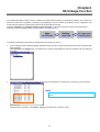
1
PALMiCE FPGA Probing Function User's Manual
This manual describes the probing function and presents the basic usage patterns.
Chapter1
Introducing the Probing Function
The probing function makes it easy for the CSIDE debugging software to connect FPGA internal nodes (signals) to pins. This
allows waveform monitoring based debugging to proceed smoothly.
The previously troublesome and time-consuming operation of modifying a source file, performing the logic synthesis/place and
route operations, and finally performing a configuration operation can now be performed simply with just CSIDE operations, and
execution only takes from under a minute to just a few minutes.
Note
The signals that can be modified or added are the signals that have placement information (that
is, the signals displayed in the CSIDE Node Location window). Signals that have been optimized
in logic circuits cannot be routed. In this case, you must either use the CSIDE ISE linkage
function (see Chapter4 ISE Linkage Function) or re-synthesize in the Xilinx FPGA
development tool ISE.
Since the actual routing operation uses the ISE FPGA editor, the ISE Web Pack is not supported.
The following section describes the probing function in detail.
1
Chapter2
Using the Probing Function
To use the probing function, first associate the FPGA pins and channels.
2.1 Associating FPGA Pins and Channels
When using the probing function, first, the FPGA pins allocated as analyzer pins must be
linked to the PALMiCE analyzer function channels. Rather than linking the FPGA pins
each time internal signals to be monitored are set up, we recommend allocating the
FPGA pins and the channels in advance. If this linkage is set up in advance, then the
following debugging operations based on repeatedly registering and changing the
monitored signals will proceed smoothly.
There are two methods for linking FPGA pins and channels.
1. Using the probing settings wizard
2. Using commands
The following section describes these two methods.
*In the figure, the FPGA pins are the pins that are actually connected to the user system.
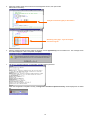
2.1.1 Linking by using the probing settings wizard
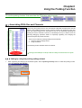
1.
When registering and changing the monitored signals, click the [Probing function] button to enable the probing function.
Then click [Analyzer Pin Settings].
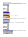
2
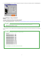
2.
The Probing Settings wizard is displayed. Register the FPGA pins according to the wizard procedure. Click [Finish] when
done registering pins.
2.1.2 Linking by using commands
This section describes the procedure for linking using commands.
Commands are entered and executed in the Command window.
Use the “StateAnalyzerChannelPin” command. (See the Command Reference section in the PALMiCE FPGA Online Manual.)
Example1
To set the FPGA pin connected to channel 0 (CH0) to chain number 1 FPGA pin number M15.
StateAnalyzerChannelPin( 0, 1, M15 )
It is also possible to set up multiple channels and FPGA pins easily by creating a macro file and executing it in the Command
window.
Example2
Macro file example: settings for channels 0 to 7 (CH0 to CH15)
{probingset
StateAnalyzerChannelPin( 0, 1, M15 )
StateAnalyzerChannelPin( 1, 1, M16 )
StateAnalyzerChannelPin( 2, 1, M13 )
StateAnalyzerChannelPin( 3, 1, L14 )
StateAnalyzerChannelPin( 4, 1, L15 )
StateAnalyzerChannelPin( 5, 1, L16 )
StateAnalyzerChannelPin( 6, 1, L13 )
StateAnalyzerChannelPin( 7, 1, K14 )
StateAnalyzerChannelPin( 8, 1, K15 )
StateAnalyzerChannelPin( 9, 1, K16 )
StateAnalyzerChannelPin( 10, 1, L12 )
StateAnalyzerChannelPin( 11, 1, K12 )
StateAnalyzerChannelPin( 12, 1, K13 )
StateAnalyzerChannelPin( 13, 1, J14 )
StateAnalyzerChannelPin( 14, 1, J15 )
StateAnalyzerChannelPin( 15, 1, J16 )
}
Enter "probingset" in the Command window and execute it.
3
2.2 Registering Monitored Signals
The following methods can be used to register signals for waveform monitoring.
Registration from the Editor window
Registration from the Node Location window
Registration from the analyzer settings
2.2.1 Registration from the Editor and Node Location windows
Registration from the Node Location window
Registration from the Editor window
Right click on the signal to be registered and select [Register in the Analyzer] from the pop-up menu.
2.2.2 Registration from the analyzer settings
Right click anywhere in the Analyzer window and select [Analyzer settings] from the pop-up menu. The Analyzer Settings dialog
box will be displayed. Signals can be registered with the [Set trigger and signal] tab. See Chapter3 Trying the Probing
Function for details.
The signals that can be registered as monitored signal are the signals that have placement information (that is, the signals
displayed in the CSIDE Node Location window).
Signals that have been optimized in logic circuits cannot be routed.
The sequence of modifying the source file, performing the logic synthesis/place and route operations, and finally performing a
configuration operation is required to monitor signals that have no placement information. However, these operations can also be
performed in CSIDE using the ISE linkage function. (See Chapter4 ISE Linkage Function.)
4
Chapter3
Trying the Probing Function
This chapter describes the probing function using a sample program.
This sample program is written in the VHDL language.
It is a simple circuit consisting of 8-bit counter and flip flop elements.
The sample program is shown here.
--Signal-signal
signal
-------------------------------------------------------------- Sample Circuit
-- Copyright 2004 COMPUTEX CO.,LTD. All rights reserved.
------------------------------------------------------------library IEEE ;
use IEEE.std_logic_1164.all ;
use IEEE.std_logic_unsigned.all ;
entity SAMPLE is
port (
CE
RESET
CK
OUT_DT
);
end SAMPLE;
: in
: in
: in
: out
CK_GCK
COUNT_DT
: std_logic;
: std_logic_vector(7 downto 0);
------------------------------------------------------------begin
UC : CAPTURE_SPARTAN2 port map (CAP => '1',CLK => CK_GCK) ;
U1 : BUFG port map (I => CK, O => CK_GCK);
------------------------------------------------------------process (CK_GCK,RESET)
begin
if (RESET = '1') then
COUNT_DT <= "00000000";
elsif (CK_GCK'event and CK_GCK = '1') then
if CE = '1' then
COUNT_DT <= COUNT_DT + '1';
end if;
end if;
end process;
std_logic;
std_logic;
std_logic;
std_logic_vector(7 downto 0)
architecture BEHAVIOR of SAMPLE is
-- ***************** COMPONENT ****************** -component CAPTURE_SPARTAN2
port(
CAP : in std_logic ;
CLK : in std_logic
);
end component ;
process (CK_GCK)
begin
if (CK_GCK'event and CK_GCK = '1') then
OUT_DT <= COUNT_DT;
end if;
end process;
component BUFG
port (
I
: in std_logic;
O
: out std_logic
);
end component;
end BEHAVIOR;
component IBUF
port (
I
: in std_logic;
O
: out std_logic
);
end component;
-- ***************** END COMPONENT ****************** --
5
3.1 Linking Channels to FPGA Pins
First, we link the channels to the FPGA pins.
In this section we describe the procedure for using the Probing Settings wizard.
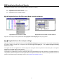
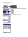
1.
Select [Analyzer] from the [View] menu in the CSIDE main window. The Analyzer window will be displayed.
Right click anywhere in the Analyzer window and select [Analyzer Settings] from the pop-up menu. The Analyzer Settings
window will be displayed.
Select the [Set trigger and signal] tab. The dialog box show here will be displayed. Click [Add] .
2.
Click [Probing function] to enable the probing function. Next click [Analyzer Pin Settings].
6
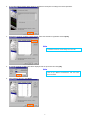
3.
The Probing Settings wizard will be displayed. Register the FPGA pins according to the wizard procedure.
4.
Register the FPGA pin numbers in each channel. Select the channel for registration and click [Edit].
Note
[Save Macro] button
This button saves the current settings in a macro file.
5.
The Modify Analyzer Pin dialog box will be displayed. Set the pin number and click [OK].
Note
[Advanced Settings] button
Sets the pin electrical characteristics. See the online
manual for details.
6.
After registering the pins, click [Next].
7
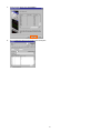
7. Verify the set values and click [Finish].
8.
This completes linking the channels to the FPGA pins.
8
3.2 Registering the Monitored Signals
Once the channels and FPGA pins have been linked, next, register the bus signals count_dt[7:0] in channels 0 to 7.
This section describes this operation from the standpoint of the Analyzer Settings dialog box. To register the signals using the
Editor window and the Node Location window, proceed to step 4 immediately.
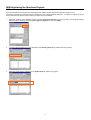
1. Right click anywhere in the Analyzer window and select [Analyzer Settings] from the pop-up menu. The Analyzer Settings
dialog box will be displayed. Select the [Set trigger and signal] tab. Then click [Add] .
2. The Signal Settings dialog box will be displayed. Click [Probing function] to enable the probing function.
3. Select the signal name to register from the [Node name] list. Select count_dt[7:0].
9
4. Select the channels to allocate. Check channels 0 to 7. Click [Registration] after the channels have been selected.
Note
The number of required channels and the number of selected channels will
be displayed. Select channels so that these two channel counts have the
same value.
BusSize = 8 / 8
The number of required channels
The number of selected channels
If [Automatic Channel Allocation] is checked, CSIDE will select the channels to use from the unused channels and
allocate them automatically.
5.
The Signal Settings dialog box will be displayed for the next signal registrations. Since we will not be registering them using
this dialog box, click [Close] to close this dialog box.
6.
The count_dt[7:0] signals are registered for channels 0 to 7. Set the trigger and other conditions and click [OK].
10
7.
A dialog box that verifies whether or not you want to have all the signal settings reflected in the window will open. Click [Yes].
8.
Start the FPGA editor and click [Yes] in the dialog box that opens to confirm whether or not you want to perform a
configuration operation.
9. The FPGA editor runs and performs a configuration operation.
When the configuration completes normally, "Configuration of FPGA completed normally" will be displayed in the status
bar.
10. The count_dt[7:0] signals will have been added.
11
3.3 Modifying the Monitored Signals
This section describes the procedure for modifying the count_dt[7:0] signals registered in section 3.2 Registering the Monitored
Signals
1. Right click anywhere in the Analyzer window and select [Analyzer Settings] from the pop-up menu. The Analyzer Settings
dialog box will be displayed. Select the [Set Trigger and Signal] tab. Select count_dt[7:0] as the signal name to be modified
and click [Change].
2. The Signal Settings dialog box will be displayed showing the current registration state.
3. Select the signals to be modified from the [Node name] list. Select "ce". The unnecessary channels will be cleared.
To allocate the ce signal to another channel, check the channel to which it is to be allocated.
12
4.
When the signal modifications have been made, click [OK].
5.
This modifies the ce signal. Set the trigger and other conditions and click [OK].
6.
A dialog box that verifies whether or not you want to have all the signal settings reflected in the window will open. Click [Yes].
7.
Start the FPGA editor and click [Yes] in the dialog box that opens to confirm whether or not you want to perform a
configuration operation.
8.
The FPGA editor runs and performs a configuration operation.
When the configuration completes normally, "Configuration of FPGA completed normally" will be displayed in the status
bar.
13
9.
This modifies the ce signal for count_dt[7:0] signal waveform monitoring.
14
Chapter4
ISE Linkage Function
The CSIDE ISE linkage function is used to register and modify signals that have no placement information. This function can
perform the sequence of operations consisting of (1) modifying the source in CSIDE, (2) synthesis, and (3) configuration. The
actual synthesis operation is performed by the Xilinx FPGA development tool ISE.
(Read the “Synthesis” and “Synthesis following Place and Route” in the online manual in conjunction with this section.)
This section uses the example used in Chapter3 Trying the Probing Function.
The following describes the procedure for registering the bus signal count_dt[0..7].
1. For the signals that were registered (added), define pins in the UCF file so that the allocated pins are routed as analyzer pins
during synthesis.
Select [Source] in the [FPGA] menu. The FPGA source window will be displayed. Open the sample.ucf file and define the
FPGA pins.
2. Define the FPGA pins. Although any names can be used for the added pins, we will use CH_CTEX(0) to (7) in this section.
Note
The FPGA pins defined here are pins that are actually connected to the user
system.
After defining the FPGA pins, select [Save] - [File] from the File menu to save the ucf file.
15
3. Select the sample.vhd file in the FPGA Source Management window, and open the file.
Edit the file as necessary.
Analyzer monitored signal pin declaration
Allocating count_dt[7 .. 0] to the analyzer
monitored signals
4. After the sample.vhd file has been edited as required, execute [Synthesize] from the FPGA menu. The message shown
here will be displayed. If this is acceptable, click [Yes].
5.
ISE will run, and after synthesis, a configuration operation will be performed.
When the configuration completes normally, "Configuration of FPGA completed normally" will be displayed in the status
bar.
16
6. Register the signals in the Analyzer window.
Select [Analyzer] in the [View] menu. The Analyzer window will open.
Either double click or right click anywhere in the Analyzer window and select [Analyzer Settings] from the pop-up menu. The
Analyzer Settings dialog box will be displayed. Select the [Set Trigger and Signal] tab. Click [Add].
7. The Signal Settings dialog box will be displayed. Disable the probing function.
8. Enter count_dt as the [Signal] and click channels 0 to 7. Next, click [Registration].
9. The Signal Settings dialog box will be displayed for the next signal registration. Since there are no signals to register at this
point, click [Close] to close this dialog box.
10. The count_dt[7:0] signals are now registered for channels 0 to 7. Set the trigger and other conditions and click [OK].
11. A dialog box that verifies whether or not you want to have all the signal settings reflected in the window will open. Click [Yes].
17
12. The count_dt[7:0] signals have now been added.
Computex Co.,ltd.
Head office
432-13, 4-chome, Gojyoubashi-higashi, Higashiyama-ku, Kyoto, 605-0846
TEL.075(551)0528 FAX.075(551)2585
Sales department
7F, DNK-building, 15-2, 2-chome, Uchikanda, Chiyoda-ku, Tokyo, 101-0047
TEL.03(3253)2901 FAX.03(3253)2902
PALMiCE FPGA Probing Function User's Manual
CM654(B)0411
18