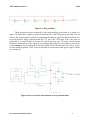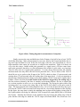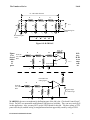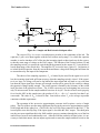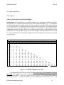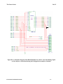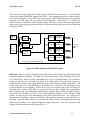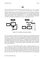
1
Lab manual as of 11/25/2010. I have introduced new labs for the later part of the course based on a Xilinx Spartan 3E-series Field Programmable Gate Array (FPGA). The first of these is Lab E on building a musicbox and the second is Lab F on building a scrolling electric sign. The manual is still only complete through Lab A plus Labs E and F. Material in this on-line version for Labs B, C, and D is obsolete. Lab F is now functional and the deadline for it will be the close of business on Wednesday, two days after the exam when I am supposed to give grades. I have also made minor changes to clarify lab 5 and the logic analyzer challenge, to correct a minor error in lab A and to clarify a point in lab F. ENGN1630 Lab Manual Fall 2010 1 Brown University School of Engineering Engineering 1630 - Digital Electronics System Design Semester I - 2010-11 The Student Lab Manual Wm. R. Patterson ENGN1630 Lab Manual Fall 2010 2 ENGN1630 Lab Manual Fall 2010 3 Table of Contents 1. GENERAL INTRODUCTION .................................................................................................................................. 6 2. EVALUATION ........................................................................................................................................................... 9 2.1. GRADES .................................................................................................................................................................. 9 2.2. PARTIAL CREDIT ................................................................................................................................................... 10 2.3. INCOMPLETES........................................................................................................................................................ 10 2.4. THE FAULT TOLERANCE QUESTION (FTQ) ........................................................................................................... 11 2.5. DOCUMENTATION ................................................................................................................................................. 12 2.6. DEADLINES ........................................................................................................................................................... 13 2.7. THE ENGN1630 EXCLUSION PRINCIPLE ............................................................................................................... 14 2.8. LAB SCHEDULE ..................................................................................................................................................... 14 2.9. TEACHER EVALUATION ......................................................................................................................................... 15 2.10. COLLABORATION ................................................................................................................................................ 15 3. GETTING STARTED .............................................................................................................................................. 16 4. CIRCUIT CONSTRUCTION GUIDELINES ........................................................................................................ 17 4.1. 4.2. 4.3. 4.4. 4.5. 4.6. GENERAL HINTS .................................................................................................................................................... 17 THE 163 LAB ENVIRONMENT ................................................................................................................................ 18 LOGIC PROBES ...................................................................................................................................................... 19 POWER SUPPLIES ................................................................................................................................................... 19 BYPASSING............................................................................................................................................................ 19 DEBOUNCING ........................................................................................................................................................ 20 5. DESIGN AND TROUBLESHOOTING ................................................................................................................. 22 5.1. DESIGN ................................................................................................................................................................. 22 5.2. TROUBLESHOOTING .............................................................................................................................................. 23 6. HOMEWORK, LECTURES, AND TEXTBOOKS ............................................................................................... 25 6.1. 6.2. 6.3. 6.4. HOMEWORK .......................................................................................................................................................... 25 LECTURES ............................................................................................................................................................. 25 TEXTBOOKS .......................................................................................................................................................... 26 SYLLABUS ............................................................................................................................................................. 26 7. SCORECARD ........................................................................................................................................................... 28 9. THE LAB CHALLENGES ...................................................................................................................................... 30 9.1. DISPLAYS AND LIGHT EMITTING DIODES ................................................................................................ 30 9.2. THE NUMBERED LABS ..................................................................................................................................... 34 9.2.1. LAB ZERO .......................................................................................................................................................... 34 9.2.2. LAB ONE ............................................................................................................................................................ 36 9.2.3. LAB TWO ........................................................................................................................................................... 38 9.2.4. LAB THREE ........................................................................................................................................................ 46 9.2.5. LAB FOUR .......................................................................................................................................................... 49 9.2.6. LAB FIVE............................................................................................................................................................ 51 9.2.6.1. Verilog Implementation of a Counter – An Example ................................................................................. 54 9.2.6.2. Assigning Pin Numbers to Programmable Devices ................................................................................... 56 9.2.6.3. Editing and Compiling Verilog Files for Xilinx Parts................................................................................ 57 ENGN1630 Lab Manual Fall 2010 4 9.2.7. LAB SIX.............................................................................................................................................................. 59 9.2.8. LAB SEVEN ........................................................................................................................................................ 65 9.2.9. LAB EIGHT ......................................................................................................................................................... 72 9.2.10. LAB NINE ......................................................................................................................................................... 78 9.3. THE LETTERED LABS ................................................................................................................................... 80 9.3.1. 9.3.2. 9.3.3. 9.3.4. 9.3.6. LAB A: ............................................................................................................................................................... 80 LAB B: ............................................................................................................................................................... 82 LAB C: ............................................................................................................................................................... 88 LAB D: ............................................................................................................................................................... 97 LAB F: .............................................................................................................................................................. 108 9.4. THE LOGIC ANALYZER CHALLENGE ....................................................................................................... 111 9.5. REQUIREMENTS FOR A SCHEMATIC DRAWING ................................................................................... 112 10. THE ENGINEERING 163 CPLD-II BOARD .................................................................................................... 116 FIGURE 10.3: SCHEMATIC DIAGRAM OF THE ENGINEERING 163 CPLD BOARD ................................. 123 11. SCHEMATICS AND TIMING DIAGRAMS..................................................................................................... 125 11.1. GENERAL DOCUMENTATION ............................................................................................................................. 125 11.2. TIMING DIAGRAMS ........................................................................................................................................... 126 FIGURE 11.2: TIMING DIAGRAM EXAMPLE. ................................................................................................................. 127 11.3. USING THE DXDESIGNER SCHEMATIC CAPTURE SOFTWARE............................................................................. 127 11.4. USING AN HDL FOR DESIGN ENTRY INTO A SPARTAN XC3S500E FPGA ......................................................... 137 11.5. USING THE SPARTAN XC3S500E EVALUATION BOARDS................................................................................... 137 12. COMPONENT DATA INDEX ............................................................................................................................ 138 ENGN1630 Lab Manual Fall 2010 5 1. General Introduction This is primarily a lab-based course. It starts with a series of simple labs getting you acquainted with the basic gates and flip-flops and how they are connected to do such tasks as singlebit addition, error correction, bus multiplexing, etc. Few real systems are assembled this way anymore but there are two virtues to these labs. First they are a simple way to let you learn the basics through your fingers. Second, you learn something about the logic of debugging circuits including finding mechanical problems. (Real systems have lots of design and reliability issues from mechanical problems, that is, trouble from unreliable interconnections and difficult design problems to build neat, compact packaging.) Somewhat more complex logic operations are feasible for you using programmable logic, one example of which is the Complex Programmable Logic Device or CPLD. The one you will use for many of the labs is the Xilinx XC9572XL, which is roughly equivalent to a few hundred basic gates. We have prototyping boards that allow you to embed these devices into larger more practical systems that you must design. Finally in the last few labs, you use an even more powerful programmable device, a Xilinx Spartan 3e™ field programmable gate array (FPGA). While the device itself has been purchased embedded in an evaluation board with a lot of support components, I am building input-output add-on boards to simplify having you design real non-trivial logic systems. Please be patient with us as I try to get these working. As part of learning the practice of the profession, we require you to use some industrial strength CAD software. You will learn schematic capture in DxDesigner, a design tool suite from Mentor Graphics Corp. This tool is one of the most popular starting points for printed circuit board design, the only feasible means of solving those pesky interconnection problems! On the other hand, we no longer use DxDesigner to do circuit simulation of discrete circuits because small scale logic is generally not complex enough to warrant logical simulation while the real issues in such designs are electrical not logical, e.g., transmission line reflections, propagation time effects, crosstalk, etc. These effects are not captured by logic simulators but require specialized simulators. You will only do logic simulation for your programmable devices, the complexity of which requires sophisticated simulation capability. (Our simulation techniques are actually applicable to fairly complex board-level designs when hardware descriptions of all the simulatable chips on the board are available from their vendors.) You do labs using Xilinx XC9572XL complex programmable logic devices (CPLDs) and XC3S500E field programmable gate arrays (FPGAs). For their simulation, we will use a mix of Xilinx software to program the devices and Aldec-Active HDL software to simulate them. With all the changes to both the hardware and software for this later part of the course, I expect that this material will not be integrated without a certain amount of difficulty I ask your indulgence. In Engineering 1630, you start by designing small systems with TTL integrated circuits, building them, and then fiddling until they work. The fiddling can go from minor rewiring to complete redesign as one gets accustomed to the subtlety of the problem. This method can be very satisfying and great fun. (Please do not assume that “fiddling” alone is the right way to design. Care in analysis and simulation is the only route to larger systems. Fiddling is simply a necessary step in learning to ask the right questions.) This is not a practical way to build larger systems so the later parts of the course introduce hardware description languages as the first element of more modern approaches. ENGN1630 Lab Manual Fall 2010 6 Your kits are largely made from “TTL” or Transistor Transistor Logic parts because these are the main commercial source of very small blocks of logic and they are quite inexpensive. But it is important to realize that TTL is not the only or even the dominant expression of logical systems even at the very small systems level. In fact, the main driver for my changing the simpler labs is that the components are so obsolete they are disappearing from the market altogether. (If you decide to keep your kit at the end of the course, you will have a pre-made antique collection.) The dominant manufacturing technology for digital circuits is CMOS - the Complementary Metal Oxide Semiconductor process, which we will examine briefly in class in explaining how gates actually do their work. For labs two and six in which you measure gate properties we will supply some TTL-compatible, low voltage CMOS parts from Texas Instruments’ SN74LVCxx series. Devices in this family are intended to supply small logic blocks for systems using power supply voltages less than the 5 volts that was standard for many years for TTL. (Most discrete logic today functions on 3.3 volts or lower.) Their working input signal range is 1.8 to 5.0 volts and they will function with supply voltages over a similar range but are optimized for 3.3 volts supply or less. You will look at their speed and power performance over the full supply range. Complex programmable logic devices (CPLDs in the trade jargon) are a competitive area of development. They are generally smaller and less flexible than FPGAs, but they are less expensive, require many fewer support components, and have fast, well-controlled propagation delays. (As with many general statements about technology, this one has to be qualified. FPGAs have benefited from the most advanced manufacturing processes. As a result their speeds are now fast enough that one has to examine particular applications to decide whether a CPLD or an FPGA will do the best job. Often the basis of choice is simply the size of the logic – fpga’s implement larger systems, albeit at higher prices. CPLDs, however, do have the curious properties of more efficiently generating simple Boolean products of many inputs and of having propagation times more or less independent of logical function. They are also non-volatile, that is, you do not have to reprogram every time you turn the circuit on.) You start to do labs with a CPLD at lab 3 and may use one again in Labs 4, 5, 7, A, and B with some restrictions. The ninth lab is on timing simulation, thus introducing the problem of verifying designs before they are built. Labs C through F are done with FPGAs. You can program both CPLDs and FPGAs either using schematic entry or a hardware description language (HDL). In both cases you are just converting your thoughts into terms that software can convert to bit patterns for the switches and floating gate transistors in the devices. In this course you will use the Verilog HDL for design entry. In the early labs, labs 3, 4, and 5, you are limited in the syntax you are allowed to use because the point of the labs is the logic not the elegance of how well you can express intent in the language. In the later labs, you are freer to exploit the full language flexibility. Wakerly (sects. 5.4, 7.13, and examples in chapter 6) has very good coverage of the basics of the language and there are other tutorials on the web. A short one tutorial that I found useful the first time I tried Verilog is: http://www.eecs.harvard.edu/cs141/resources/verilog-tutorial.pdf. The emphasis throughout Engineering 1630 is on the design, construction, and verification of digital circuits. In class, we will discuss the conceptual and physical building blocks available to ENGN1630 Lab Manual Fall 2010 7 the designer, and show how these tools and techniques are used in various design situations. In the lab, you will take this design theory and put it to use by building actual hardware-based solutions. This may well be your only exposure to full responsibility for making a product work ever! (Engineering, like Computer Science, is a surprisingly social endeavor - most products come from development teams, not isolated geniuses.) Reflecting the fact that this is primarily a hands-on laboratory course, many of the customary requirements of engineering courses have been scaled down. There are only two lab reports and one schematic to compose, and these will be graded on a satisfactory/must be redone basis. The computer simulation lab and the logic analyzer exercise will be at least partially self-documenting. There are only minimal fixed deadlines for individual assignments. While there will be a midterm and a final examination they are intended to encourage you to think of the lab material in a more general framework. Your grade will be calculated as an average of your lab grade and the two exam grades. We expect the exams to test how well you respond to freshly posed problems of a similar nature to those found in the labs. In the lab you design and build a particular circuit and then demonstrate that system to one of the TAs. You must be prepared to show a schematic of your system drawn with your own hand or through your own schematic entry and to explain it to the TA. The TA must be satisfied with the quality of that documentation before he/she will examine the rest of your work. After studying your approach, the TA will ask you a question about its performance or its design; if you answer the question correctly, the TA signs your scorecard, and you are free to move on to the next lab challenge. In this course there are no specified times when you have to appear in the lab. You may design and build your circuit wherever you like. We will provide the necessary equipment to test and debug your circuit and will also provide a group of well-qualified teaching assistants to help you with any unusual problems. If you run into problems with malfunctioning equipment or software, please bring it to the attention of a TA or to me. The liberalized format of ENGN1630 presents you with a number of challenges quite apart from actually building each lab assignment. By the time you take this course (typically in the junior or senior year) we expect that you have learned to think creatively, to work consistently, and to budget your time. The minimal deadlines established for completion of the labs force you to set goals for your own performance. While many design techniques are discussed in class, it is your responsibility to put broad concepts into practice. Making choices is part of the process. Class will meet on Mondays and Wednesdays, from 3:00 PM until about 4:20. The lab will be open day and night most of the week with TA coverage for about 40 hours per week, with convenient evening hours twice a week. The lab will be in the Hewlett Electronics Laboratory, room 196 of the Giancarlo addition. You are not required to attend class, although I hope that the relatively small class size will make the lectures more attractive. Similarly the relevant readings are optional. We do not wish to waste your time by forcing you to sit through boring lectures or to read irrelevant ramblings meant to up the page counts of books. However, the TAs are not obliged to repeat lecture or text material to exempt you from learning it on your own. ENGN1630 Lab Manual Fall 2010 8 2. Evaluation The evaluation policy used in ENGN16300 changes with the convictions and whims of the instructor in charge. Some take a rather liberal approach, allowing your circuits alone to represent the depth and breadth of your digital logic design knowledge. Some lower the lab weighting to make room for formal homework assignments. Others of us use points-oriented grading schemes of Baroque complexity that make your final grade dependent on how well you score on mid-term and final examinations, in addition to the number of design exercises you complete. Each of these approaches has its benefits, and each has its drawbacks. I follow a grading policy based on a point system. There will probably be a total of 165 points available, 65 points from exams and 100 points allocated for completed lab work as tabulated below. To some extent the exact number of points will have to be adjusted based on how many of the later labs I can get functional in time. I reserve the right to change the total number and their weight depending on how much I get done. Passing performances on both exams and lab work separately are required to pass the course, but a curve will be applied to your total grade to determine the letter grade reported to the Registrar. I expect that an A will require about 135 points and a C will cost about 80 points. These boundaries have served me fairly well over the last couple of years. 2.1. Grades Your lab grade is based on the number of lab challenges you complete. There is no partial credit on the lab grades. Instead you will receive points for each successfully completed lab challenge or piece of written lab work. There are 16 hexadecimally numbered labs of which you may do up to 15, including only 3 from C, D, E, and F. With the points for using the schematic drawing software and the logic analyzer, there are a total of 100 possible lab points. The distribution of points is: Lab 0 through Lab 5: 5 pts. ea. Lab 6 through Lab 8 and software simulation Lab 9: 6 pts. ea. Lab A and B and up to three from the group Labs C, D, E, and F: A schematic for either Lab 1, 7, 8, or B: 7 pts. ea. 6 pts. Logic analyzer measurement challenge (see section 9.4): 5 pts. To pass the course, however, you must have passing grades on BOTH the examination and lab parts of the course. A passing grade on the examination part of the course is 48% of the sum of the maximum number of points possible on the exams. A passing grade on the lab part of the course is 53 points, which must include credit for Labs 1 and 2; for one lab from the set 7 and 8; for Lab 9 and for one lab from the C through F series; for the Logic Analyzer Challenge, and for a ENGN1630 Lab Manual Fall 2010 9 schematic of either lab 1, 7, 8, or B. THERE WILL BE NO EXCEPTIONS TO THIS POLICY. Please note that the use of a logic analyzer is mandatory. The laboratory has a superb collection of instruments and their use is to hardware what a debugger is to software. You don't know much about either discipline without knowing its fundamental test tools. A word of advice: labs 7 and 8 involve systems with mixed analog and digital signals. Many students find these labs time consuming because they find it difficult to be systematic about dealing with the analog part. The letter series labs may also take significant amounts of time. However, they are purely digital. If you find that the first analog-to-digital converter lab that you do takes too long, then do the letter labs next. Only do the other A/D lab if you have time toward the end of the course. Scuttlebutt variously suggests that either lab 7 or 8 is much easier than the other. I believe they are about equal difficulty. (I have changed some of the parts and requirements on lab 7 to make it easier to do than it used to be.) A careful and systematic approach is critical to success within reasonable time limits on either of them. The use of simulation for the digital section in advance can save enormous amounts of time on these labs and will provide a basis for logic analyzer measurements comparing expected and actual performance. Section 7 of this manual contains a scorecard for recording your performance on each of the labs; each time you successfully complete a lab, a TA will sign the line associated with that challenge and make an entry on our backup sheets. To receive your grade, you must turn in your scorecard at the end of the semester, which is defined as no later than 5:00 PM of the day of the scheduled final examination. Do Not Lose Your Scorecard!!! We try to keep duplicate records, but the backups are hard to search, and there are NO guarantees. People who arrive empty-handed at the end of the semester will receive No Credit for the course. 2.2. Partial Credit The nature of ENGN1630 precludes the assignment of partial credit for any of the Labs. If, for example, you are told to build a circuit that displays the digits 0, 1, 2, 3, 4, 5, 6, and 7 in a particular order, and you offer a circuit that displays all but the digit 3, you get no credit for the Lab until you troubleshoot the circuit and get it working as requested. This policy just reflects the nature of digital system design, and it is one from which no deviations will be made. 2.3. Incompletes No grade of Incomplete for unfinished labs will be given unless you present evidence from a physician or a Dean of a serious and protracted medical problem. Because of the nature of the course, there is no way of dealing with students after the end of the semester. The TAs are gone, the lab space is reorganized and used by other courses and other students, and all parts must be checked, cleaned, and inventoried. If you need to pass ENGN1630 to complete the departmental requirements for a specific Brown degree, make sure you at least qualify for a grade of C. I have no sympathy for someone who shows up at the end of the semester with a nearly-blank scorecard in hand, and claims that he or she needs this course to graduate. The time to consider the relative importance of ENGN1630 to your educational experience is now. ENGN1630 Lab Manual Fall 2010 10 2.4. The Fault Tolerance Question (FTQ) When you demonstrate a circuit for a TA, you and the TA will spend a couple of minutes verifying that the circuit meets all requirements. You must then show a schematic and explain the operation. (NOTE: This procedure is another change from prior years.) The schematic does not have to be machine generated although that would be preferable. It does have to be both neat and accurate. If you are asked where a particular connection point on the schematic is and reply that well you changed that, then you get to go away and do the documentation over again. The TAs get to decide whether the drawing is neat enough to understand. The TA will then check your breadboard serial number and ask a Fault Tolerance Question (FTQ). These questions may take one of three forms, at the option of the TA. For the first type of question, the TA will choose one wire in your circuit and ask what, if anything, will go wrong with your circuit after the wire is removed. For the second type of FTQ, the TA will introduce a problem into your circuit, leaving you the responsibility of finding and correcting the problem. The third type of FTQ will allow the TA to ask you general questions about the operation of your circuit, such as “What will happen to the output of the Q1 flip-flop if both inputs to this NAND gate are grounded?” It is a TA's prerogative to ask for documentation before an FTQ. These notions of an FTQ are based on TTL implementations of small systems. The labs based on programmable devices (CPLD or FPGA) pose special problems for framing good FTQs. In preparation for an FTQ or even for certification of compliance with specifications, you must make a printed copy of the Verilog file, the Xilinx logic schematic, or the Active-HDL block diagram source file in addition to the wiring diagram. At the least, the TA will want to see this and ask how you designed it. She may ask variants on the hardware FTQs based on changes to operation of the circuit that will be caused by a change to the schematic, VHDL, or Boolean description and may expect you to compile and demonstrate the expected result on the spot. Because the equipment for the FPGA labs is new this year, we may have to change the FTQ procedure as we gain experience. If you answer the FTQ correctly, the TA will sign your scorecard, congratulate you, and you can celebrate! (As a precautionary measure, you might want to be sure the TA enters your success on the backup sheets just in case you lose your scorecard.) If you do not answer the FTQ correctly, the TA will be obliged to ask you two more FTQ's. For every FTQ that you miss, two more must be asked. If several FTQ's are answered incorrectly, we will begin to wonder how you can know so little about a circuit that you designed, built, and tested yourself. We will begin to wonder about plagiarism. If you miss three FTQ's in a row, your circuit breadboard will be temporarily confiscated and you will be referred to the head TA for further consultation. If you are guilty of demonstrating a circuit that someone else designed, you will automatically lose credit for that lab. (If this is a required lab, you may not be able to pass the course.) If a second offense occurs, standard academic discipline procedures will be initiated. We are aware that a certain amount of shopping around is done by students looking for a soft-hearted TA. To limit this behavior, no one can have more than five labs checked by any one TA. All the TAs will have been told that we regard FTQ's as serious matters, and no TA has to be a patsy. ENGN1630 Lab Manual Fall 2010 11 For most of the labs, once an FTQ (or a series of FTQ's) have been answered correctly, you have met all the requirements for that lab. There are a few exceptions to this rule. Labs 2 and 6 involve the measurement of important properties of your chips, such as power dissipation, logic levels, propagation delay, etc. They require data and the answers to some questions to be handed in as a report in lieu of an FTQ. These write-ups will be graded only on a satisfactory/must-becorrected basis and will be handed back only after all reports for that lab were due. You must both take the data and write the report individually! It is perfectly okay to give each other advice and information, but you are responsible for doing your own work. Similarly lab 9 on simulation and the schematic drawing by computer design entry require documentation in lieu of FTQs. All documentation is handed in through a box in room 196. We still have to mark that with an appropriate sign. An FTQ can be fairly difficult sometimes. We will try not to choose bizarre wires or concoct impossible-to-analyze situations. In any event, you are responsible for giving a complete account of impending faults in your circuit before the wire is pulled or the software program modified. If you mention that X and Y will go wrong, but only X goes wrong when the wire is pulled, your answer is incorrect. On the other hand, if you mention that X and Y will go wrong, and X and Y and Z actually go wrong, then your answer is also incorrect. In some cases, you may want to list contingencies: “If the input goes HIGH, then X will occur, but if the input goes LOW, Y will occur.” This may be particularly important for CMOS circuits for which an uncommitted input is not in a well-defined state. Vague answers, like “the circuit will not work” or “it would take a scientist to figure it out” are not acceptable. Neither is going to lunch; once an FTQ is asked, you must answer it during the same session. Any interruption in the FTQ process between a question and an answer will be recorded as a question failure. You may not break off a losing streak of questions without leaving your breadboard and a record of the missed questions with the TA for passing on to the next TA who takes up the questioning. You may only break off such a streak for good cause, and ignorance is not a good cause. Be sure you understand your system before you ask for an FTQ. The TA may pass you on to his or her successor if there is a shift change during your questioning. It is the privilege of the TA to choose an appropriate FTQ. If you feel that you have been given an unfair question, first try to work out an answer. If you fail the question, you may bring your complaint to me. If I feel your complaint is justified, you will be asked a single replacement question; otherwise you will be referred back to the original TA who will ask the normal twoquestion FTQ follow-up. Because an FTQ may be non-trivial, take a reasonable amount of time to answer a question. Allocate at least fifteen minutes to this process. Do not let the atmosphere of the lab make you anxious - getting the first question correct can save you a lot of time. We expect that over the course of the semester you will spend from 2 to 4 hours answering FTQs. 2.5. Documentation ENGN1630 Lab Manual Fall 2010 12 Proper documentation is an essential aspect of the design process; I expect you to get in the habit of specifying your circuit completely while you are devising and building it. Circuit diagrams, written circuit descriptions, timing diagrams, truth tables, etc., are the counterparts in hardware design to the documentation of computer programs which is so much a part of satisfactory programming. To encourage good habits in this area, we are requiring a carefully done schematic for one lab you have completed. (You may not hand in documentation for a lab that does not work! We may reject a schematic for a bad design even though you may have gotten it past a TA. For example, some people carefully adjust components to get a poor design to work for a while. That may fool a TA sometimes, but it may not fool the one who grades a stack of schematics.) The schematic must be done using the DxDesigner computer aided design (CAD) package. You must also use the same tool to generate a Bill of Materials for the circuit including adding information on the particular parts in the circuit at the level of commercial availability. See section 9.5 for the full set of requirements. We may even require redrawing if your schematic has a poor esthetic layout even if the interconnections are correctly expressed. Please see section 11.2 for information on timing diagrams for lab 9 and section 11.3 for further information on how DxDesigner works. Also, you cannot expect much professorial or TA help with a non-working breadboard unless your working drawings are reasonably complete and legible. The TAs have been instructed not to answer questions about circuits unless they see a reasonable amount of documentation and to require a schematic as part of the evaluation process. 2.6. Deadlines Many years ago, I experimented with deadlines for general groups of labs. As a result of its success in retaining the sanity of both students and TAs during the course, I continue the tradition. The lab groups, and associated completion dates, are: Group one: Labs 0 through 3 may be checked off only until October 13, 2010. Group two: Labs 4 through 9 may be checked only until November 20, 2010. Group three: Labs A through C, and the schematic diagram requirement may be checked off only until December 6, 2010. You may obtain credit for the labs within each group only up to the posted date. (Note that labs may be completed as soon as you wish, but they must be completed by the given enpumpkination date.) The last week before the final exam will be a grace period. During this week, you may have up to one additional lab from each group checked off. Labs D through F may be checked off at any time until the last day of the semester. This year, the ENGN1630 exam comes in the middle of exam period, on the morning of Monday Dec. 13, 2010. I will allow labs to be checked off until the day after the exam since that is the latest that ENGN1630 Lab Manual Fall 2010 13 grades can be integrated before I have grades due. However, keep in mind that TA assistance and availability for FTQ's decreases during exam period for the obvious reason. The completion groups were instituted for several reasons. First, ENGN1630 is allocated a fixed amount of lab space, a small number of TAs, and a finite amount of circuit testing, troubleshooting, and demonstrating equipment. It has been our experience that most people (including me!) tend to procrastinate when not confronted with fixed deadlines. Without deadlines, some students fall hopelessly behind by the end of the semester. A second compelling reason for the institution of the deadline approach, however, is that by concentrating on a group of labs in a given number of weeks, help sessions can be scheduled as necessary to assist those who appear to be having difficulty. By monitoring progress on individual labs, we can get an idea of how people are coping with the given challenges. Note that students who thrive on the excitement generated of trying to complete the course at the last possible moment will especially appreciate and benefit from the deadline approach, since there are now four “last possible moments” to contend with instead of only one! 2.7. The ENGN1630 Exclusion Principle For each day that the lab is open, you may have only one lab signed off. This will still allow ample time to complete as many labs as you wish - after all, the typical academic semester has at least 70 class days but only 15 or so labs have been defined for the entire course. The Exclusion Principle has two purposes: one, it prevents one individual from monopolizing TA time, and two, it provides more incentive for you to learn to work efficiently and steadily rather than in bursts. Deviations to this policy will not be considered. Please note that this has implications for how much you can hope to get done in the end-of-semester grace period. 2.8. Lab Schedule The ENGN1630 lab will be in Giancarlo room 196, the Hewlett Electronics Laboratory. It will be open every day while the University is in session. Use the door nearest the ramp out of the building as its electric lock will be open. Please do not leave the other door open or unlocked. TAs will be available for some 30 plus hours a week including at least two evenings during the week, probably Wednesday and Thursday. We will try to keep TA schedules posted in the lab and on the web, telling when each TA will be available for troubleshooting help and for checking off labs. No TA will be assigned to work when class is in session. Also, although we will try to keep most lab slots staffed with at least one TA, there will undoubtedly be times when the lab has a TA scheduled but he or she does not turn up. The TAs have job interviews and other personal obligations and while I ask them to arrange for substitutes, this is not always practical. Do not schedule yourself so tightly that you miss getting a lab signed off because a TA overslept. The responsibility for getting labs checked off in a timely fashion is yours, not the TA's. ENGN1630 Lab Manual Fall 2010 14 You are encouraged to come to the lab at times when the crowd is small (such as 9 AM:) you will get more attention and have shorter waits for lab sign-offs. 2.9. Teacher Evaluation Besides my obligation to evaluate you, you will have an opportunity to evaluate me at the end of the semester. The School of Engineering arranges for both web-based and paper evaluations of teaching. It distributes an official form that is used for class assignment, salary adjustment, and (occasionally) tenure review. There is also a form designed to measure whether I have met the course goals for ABET. (Those goals are listed on the handout you receive the first day of class.) Finally, I distribute forms for the Critical Review. I take these reviews quite seriously, and would appreciate your doing the same. (By the way, I do not read any of them until after the final exam. The Dean's office retains all forms and tabulations until after exams are over and grades are submitted.) 2.10. Collaboration Unlike some courses, you are welcome to collaborate with your fellow students during the semester. Discussing problems with a friend is a good way to troubleshoot your circuit, and can be a source of self-improvement for both of you. Be sure that you completely understand any advice offered by anyone, however, since this advice may be wrong - providing even more frustration than the original problem that you yourself devised. Make sure that you will not be stumped on an FTQ. In general, two kinds of collaboration can be distinguished: soft collaboration and hard collaboration. Soft collaboration is a perfectly acceptable process of seeking and offering advice on the design of a particular lab solution. We assume that you will understand any advice given, and hence will benefit from the information exchange. Note that while you may get design help from a friend, you must use your own kit to construct the solution, you must generate your own documentation, you must be ready to explain your system with understanding, and you must answer your own FTQ. Hard collaboration means the use of another person's circuit board, wiring, or documentation during your FTQ. It also encompasses blind copying of another's design without sufficient understanding to pass the FTQ process. In labs requiring computer files, you must generate your own files individually, making your own choice of variable names, comment records, indentation, etc. All the data and reports for labs 2 and 6 and the schematic must be done individually. I will take a very dim view of nearly identical reports or duplicate data. Copying is hard collaboration! None of the forms of hard collaboration will be tolerated. If you feel compelled to use a friend's design for a given lab challenge, you must at least go through the process of making your own schematic from scratch not Xerox, wiring up the solution (including going through the computer entry process for PLD or FPGA designs), and debugging it yourself! All the wiring and troubleshooting associated with lab challenges must be performed on the circuit boards issued to you at the beginning of the semester. TAs will be required to match the numbers found on your scorecard with those on the back of your boards. If you are found using someone else's board, you will automatically lose credit for the lab you are trying to demonstrate. (If this occurs during one of the ENGN1630 Lab Manual Fall 2010 15 labs required to pass, you cannot possibly pass the course.) You may also get your friend in trouble for loaning his or her boards. In serious cases, you may be referred to the appropriate Dean for action by the Academic Code Committee and will probably receive a grade of NC for the course. Penalties for tampering with someone else's board or kit will be dealt with even more stringently. Improper collaboration, besides wasting the four thousand-plus dollars you pay for taking this course, is a serious matter and will not be tolerated. 3. Getting Started You will receive your own chip set along with this lab manual. Look over Lab 0, work out a solution on paper and test it conceptually until you are convinced it will work. Then assemble and test it. Be especially careful about connections to the power supply. The easiest way to damage a chip is to get the power supply connections backwards. The +5 volt supply lead must go to the VCC lead of each device, and the ground or 5 volt return lead must go to the GND pin of each device. If you are using LVTTL parts, be careful not to apply an overvoltage. Failure to be careful may result in wholesale damage to your chips. We realize that some of your chips may be defective as a result of prior use, but we will not replace components damaged by carelessness without some charge. Another point to be especially careful about is not to connect the output of a chip to +5 volts or even worse connect any pin of a logic chip to plus or minus 12 volts as may happen in labs 7 or 8. (Chips usually are more tolerant of outputs accidentally connected to ground.) In the labs the use the CPLDs, which is half the labs and most of the required one, you must program the device before you connect it to other wiring. We have special cables on the power supplies so you can program the XC9572XL. Then turn off the power supply, wait a moment, remove the power cable and substitute yours. Hot-swapping cables can damage CPLDs too. Always turn the power off and wait a few seconds before removing the cable to the CPLD board and never connect the cable with the power supply turned on. Nota Bene: Massive destruction of chips or melted or burnt areas on protoboards or keypads will result in appropriate adjustments to the price at which we will buy back your kit. Your keypads are mechanically very robust, but they can be ruined easily by using them to short out the power supply, i.e., to connect VCC to GND. This melts the plastic film under the buttons, causing them to stick. You must use limiting or pull-up resistors with the keypad. We are not sympathetic to damaged keypads. When you are sure the circuit works properly, find a TA, demonstrate it, explain it, and answer an FTQ. With this signoff, you are well underway! Remember the deadline system, and remember that the lab gets busier and the challenges harder as the semester progresses. If Lab 0 has you baffled, if you do not know who Herr Georg Ohm was (and why he is remembered -- his lab equipment is carefully and reverently preserved in the Deutches Museum in Munich), if you do not know the difference between voltage and ground or capacitance and resistance, do not despair. Help sessions are scheduled throughout the semester. The early sessions will provide a practical explanation of electronics, and should allow you to get started. Among other things, we will explain how a breadboard works, how to strip wire, how to distinguish beENGN1630 Lab Manual Fall 2010 16 tween capacitors and resistors, and how to use power supplies and logic probes. One purpose of ENGN1630 is to remove the mystique associated with digital hardware. Throughout the course you will have every opportunity to have your fears explained away; your responsibility is to take advantage of the help available. 4. Circuit Construction Guidelines 4.1. General Hints Be a little compulsive. Organize the components in your chip set so that you do not waste time looking through the entire lot each time you need a particular chip. If you sort them in numerical order, you will easily find any part you need. You should also lay down a piece of aluminum foil to press onto the pins of the CMOS chips; this will short their pins together and prevent the chip from being destroyed by high-voltage static electricity. (CMOS parts including CPLDs are the most vulnerable parts, but TTL parts can be damaged too. The foam we use for kits is pretty good without aluminum foil, but be careful if you substitute other materials.) Another suggestion is to make a set 3x5 index cards that summarize the pin connections and logical functions of each of the chips in your Kit. This may cost a bit of time now, but it will save time in the long run. These cards will serve as handy references on how each chip behaves, and will allow you to avoid leafing through your lab manual each time you need to know how the chip works (especially during the answering of FTQ's!). The automated form of this is to make use of the DxDesigner libraries and draw everything on-line. In general, you should start a lab challenge by working through the requirements of each subcircuit. Construct truth tables, if appropriate, showing the relationships among the various inputs and outputs of your system. Try to decompose one large problem into several smaller problems, keeping in mind the limitations of your chip selection and the need to integrate each of the pieces into a whole. Once you understand what needs to be done, work out a complete penciland-paper solution. Simulate the circuit by hand to see what happens during various combinations of inputs. Make sure that most of your logic errors are caught while you are still working in a pencil-and-paper mode; it is easier to erase a connection than to fix a circuit. You may wish to use DxDesigner to turn your hand sketch into a full schematic. This will help with accuracy of pin assignments, with finding missing signals, and with legibility. Further testing by simulation at the design stage is standard practice and is much recommended. With practice, the time to draw and simulate a circuit is short enough that it is completely offset by the time saved in construction and debug. Remember that neat drawings help you work out ideas and build things with minimum errors. Per the comments above, this effort will also guarantee better help from TAs or from me. After designing a solution, build your circuit gradually. Isolated sub-sections of the design can then be tested apart from the rest of the solution. If your circuit evolves in a step-wise manner, you will be able to understand its operation better, and you will be less likely to be baffled by a hard FTQ. When you assemble your circuit, do it neatly with wires that are not so long that they rise above the breadboard in a confused mass. Make sure that only a minimum of bare wire is exposed throughout your circuit; this will cut down on intermittent problems that result from improper insuENGN1630 Lab Manual Fall 2010 17 lation. Do not make wires so short that they loop tightly over the top of individual chips, however, since this will prevent you from exchanging a chip if it fails. (This also prevents testing it or attaching a logic analyzer to it if you suspect it has failed. Logic analyzer connections are usually made with a clip that fits over the chip. Wires over the chip prevent doing this.) The CPLD board has a special connector to make connections to the logic analyzer. Assigning pins to make that connection give a proper analyzer display can help too. When you wire a circuit, use a consistent color-coding scheme. For example, make all +5v lines red, all ground lines brown (or any other Earth tone, for that matter), etc. To aid in troubleshooting, use a variety of wire colors throughout your circuit so that co-located wires can be easily distinguished. For parallel lines of information (busses) you may want to use wire colors corresponding to the resistor color code.1 4.2. The 163 Lab Environment Besides being the place where your circuits will be tested by TA's, room 196 is where you can go to use a power supply and logic probe for troubleshooting, to talk with fellow students about the lab challenges, and generally to bask in a high-tech atmosphere. Do not, however, make a nuisance of yourself! No loud social gatherings; no smoking; no drugs; no food fights or practical jokes. Observe normal lab courtesy. Turn off equipment when you are done. Return all wires and cables to their normal places. Clean up little wires or scraps of paper. Do not remove anything from the lab (except for your lab kit) without permission. If you break something, or notice something is broken, notify a TA. OF PARTICULAR IMPORTANCE: place all parts of any broken leads for the scopes or analyzers in the boxes provided for them. These leads are very expensive ($5 apiece for the analyzers) and can often be repaired at no cost. Check the whiteboards for the latest news concerning the course. If there is a change in the lecture schedule, or if some particularly useful lab information is discovered (such as the opening or closing of the lab at non-standard times), it will be posted there and on the class web-site. For some labs, you will want to use an oscilloscope to monitor rapidly changing voltages. If you do not know how to use one, please ask a TA. He or she can explain time bases, vertical calibration, triggering, dual trace operation and other features. Because TAs are only a year ahead of you, they may not know all their details. The manuals for scopes are in the lab -- be persistent. Please be careful when using the scopes – be especially cautious with the probes. These probes are easy to damage, and cost $ 110 each to replace. Similarly the logic analyzers have delicate probes that need care in handling. Each little wire from the analyzer is five dollars to replace, and the ends break off them very easily. We have some spares but cannot afford huge quantities. If one breaks for you, please PUT THE BROKEN END AND THE WIRE ITSELF in one of the boxes we keep for that purpose. We can easily repair the probes if we get the pieces back! There are a number of manuals in the lab with the analyzers that discuss the instruments in detail. Check the drawers in the back of the room. On the other hand, we do have a good supply of leads and clips, and you shouldn’t have to jury rig everything. Ask the TAs to get more leads from me if the supply is getting low. 1 The resistor color code is a series of color and digit assignments. See the back of the data sheet section of this manual for the code’s definition. ENGN1630 Lab Manual Fall 2010 18 There are 16 PCs on the workbenches in the lab to support the labs and they run from the same server as the Computing Facility uses. Please resist the temptation to customize the desktops or to install games, email, etc. It goes without saying that the University strictly prohibits the installation of pirated software. All such entrepreneurial effort just makes our lives more complicated in keeping a common core of dedicated software working properly. If you are unfamiliar with any other pieces of equipment in the lab, ask a TA for assistance. 4.3. Logic Probes Most of the power supplies are equipped with logic probes that can quickly tell you the voltage levels of any point in your circuit. The LOW LED is on for voltages less than 0.8v; the HIGH LED is on the voltages greater than 2.4v. If the logic probe measures voltages between 1.0v and 2.2v (or if it is unconnected) no lights will glow. A third LED will light if the probe detects a pulse train. 4.4. Power Supplies The 163 lab room has approximately sixteen circuit testing stations. The heart of each of these stations is the power supply. To activate your circuit, connect a wire from the +5v terminal (or from the +12v, -12v or +3.3v as appropriate) to the appropriate slot on your breadboard and a wire from the ground terminal to your ground pins. Always double check that you have the proper polarity of power before turning on your circuit. Reversing the power supply leads could damage all of the chips on your breadboard! For your own reasons, you may wish to avoid the bustling atmosphere of the 163 lab and instead test your circuits in the privacy of your own room. The advantages of this approach are that you will be able to control the noise level around you, and you will also (presumably) be able to control the size of the crowd waiting in line for you to finish. The disadvantages of this approach are that there will typically be no TA to offer advice, and that an alternate source of 5 volt power is necessary. There are a number of solutions to this latter problem. Because supply voltage fluctuations cause circuits to malfunction and because TTL circuits draw large currents, any approach based on batteries is a marginal solution to your problem. The parts for a simple power supply can be purchased from Radio Shack for about $20. If you are interested in building one, I can give you a circuit diagram and some guidance on how to do it. For more money, it is possible to purchase a fully assembled 5v power supply that will deliver 1 or more amps of current. For example, a 5v/5A supply with auxiliary +-12-15v outputs costs under $ 40. 4.5. Bypassing No power supply is perfect in the sense that a constant potential difference of exactly +5v is present between every pair of connections to VCC and GND on every extension of every wire of the power-to-ground system. The relative immunity of digital systems to extraneous potential variations (noise!) is a major reason for the ubiquity and power of digital logic, but that immunity is ENGN1630 Lab Manual Fall 2010 19 not infinite. Because of small series resistances and inductances associated with the power supply and its wiring, noise, that is, transient current spikes generated by pulse circuits or by TTL gates changing state, can cause voltage changes on the power wiring and make your logic circuits malfunction. Sequential circuits -- counters, flip-flops, etc. -- are especially sensitive. Other noise may come from equipment turned off and on somewhere else in the lab or from the 60 cycle noise generated by fluorescent lights, or from reflections of signals sent over long wires in your circuit. (In fact, a major subdiscipline has grown up around designing out problems with power and signal distribution. It goes by the name of signal integrity analysis and design.) To protect your circuit from transient voltage spikes on the power supply lines, you can “bypass” or “decouple” the power supply by placing capacitors directly from power to ground at key places in your circuit. Key places are typically clock pulse generating or clock pulse receiving chips, such as oscillators, multivibrators, counters, flip flops or other state machines. You have several 0.1μF capacitors among your parts that can be used for bypass. More are available if necessary. Because it takes an appreciable amount of charge to change the voltage across such a capacitor, these will divert some of the current causing voltage transients. Be aware of the possibility of bypass problems when troubleshooting your circuits! If a counter seems to skips values or a flip-flop changes state for no logical reason, a bypass capacitor from VCC to GND at that chip may be necessary. Please be aware too that the 74ACT04 chip may be a source of extra noise and may require its own bypass capacitor. All except the simplest labs require at least a couple of bypass capacitors. One other possibility to check when troubleshooting an erratic circuit is that the supply voltage at the chips may be less that the 4.75 volts required for proper operation. Measure it directly at the chip with a multimeter. 4.6. Debouncing Mechanical switches, such as those on your keyboard, are another source of unwanted pulses. Suppose you press one of your keyboard buttons. Initially, the two internal wires are separated (or form an “open circuit”). Pressing the button will close the circuit, and cause contact between the two wires. Instead of making a single continuous contact, however, the two wires actually make several bouncing contacts on a microscopic scale of millisecond duration. Looking at the event with an oscilloscope you may see a series of pulses instead of the single pulse you desire. Figure I illustrates this problem and shows a method of debouncing a 2 wire push button. The solution idea here is similar to the solution of the bypass problem. Use a capacitor to absorb some of the current associated with the unwanted pulse activity. In Fig. I, we have a large resistance connected from the power supply to the gate of an inverter. If there is no other current at that logic gate input, the capacitor will remain charged to the power supply voltage. If the gate input is grounded, as it can be with the push of a button, the gate voltage will change immediately. If mechanical bounce occurs, and the contacts momentarily part, the capacitor will recharge with a time constant of about R C . The actual time this circuit takes from the opening of the switch contacts until the signal V A crosses the inverter threshold depends on the type of inverter. In lab 2 you will find that TTL gates have substantial current flowing thru input terminals. These currents charge the capacitor faster than the resistor alone would. With 74LSxx series gates, C must be several microfarads to get a 10 ms. hold time. If the gate is a CMOS gate, then it usually has no steady input current. In that case, an RC time constant of 10 ms as in Fig Eq II would result in a hold time of 3 milliseconds. [The exact result is t -R C ln(VCC VTHG ) /(VCC ) .] If, well before the 3 milliseconds elapse, mechanical contact is made again, the gate voltage will again drop to 0v and ENGN1630 Lab Manual Fall 2010 20 be kept below the threshold that causes a change of state for the gate. Thus, the output of the gate will remain low in spite of small changes going on at the input due to mechanical bounce. You may first encounter the need to put this theory into practice in Lab 4. VDD VDD 100 K 100 K Schmitt trigger inp. Pushbutton VO 0.1 uf. Pushbutton Upper thresh.. vA vO VO vA vO Time Time Figure I: Debouncing a single-contact mechanical switch or button. When the mechanical signal source is a switch instead of a pushbutton, an alternative method of debouncing the switch signal is available. Figure II shows two variants on the technique, one using the preset/clear lines on a flip-flop and the other using two NAND gates connected as an RS flip-flop. The idea is that the SPDT switch bounces on the make or break of the moving contact with either of the two stationary ones but does not bounce back and forth from the one to the other. The flip-flop responds to the first time each contact is made and ignores subsequent bounces until the other contact is closed again. From your point of view, what we hope you will notice about the devices in your kit are the input currents, and the power versus frequency relations. One of the important results of the difference in input currents is that TTL devices have uncommitted inputs which are always high, while CMOS devices have undetermined values for uncommitted inputs. Also, this behavior and the high power supply noise of the newer CMOS parts can make them not interchangeable with TTL despite having nominally identical interface specifications. It is good construction practice never to leave an input floating; connect it to either VDD or GND. Good design tools will flag such open pins as errors during design checks. Also with your CMOS parts, as with the TTL parts, it is very important to bypass power connections. VDD VDD 21 ENGN1630 Lab Manual Fall 2010 CLR D Q Figure II: Using flip-flops to debounce an SPDT switch. 5. Design and Troubleshooting 5.1. Design You may find throughout the course that inspiration is not enough to keep you working on lab challenge designs. Develop a moderate weekly schedule for steady progress. Your goal could initially be to design or build a lab solution during each session, although later labs may require considerably more time and effort. Do not find out the hard way that necessity is not always the mother of invention, especially at 4:30 pm on the last day you can get a certain lab checked off. However well you organize your time, you may still be frustrated by problems. The problems will be related to either incomplete circuit design, sloppy construction, or unsystematic troubleshooting. Design problems can be approached in one of two ways. First, you can wait for inspiration to strike. This may involve re-reading a lab challenge, and then taking a walk in the rain. (A shower may be substituted on those occasions that the sun shines for several successive days in Providence.) At the end of your walk, you may have subconsciously thought about the problem enough to have a good first approximation for a solution. A second approach may be to sit down somewhere and think very hard about the nature of the problem and how it might be solved. You can read the recommended texts for the course. You could talk to friends. You might even pay attention during lecture! Another good approach might be to study the actions of various chips in your kit, and see if this provides a clue to how a problem may be solved. Try to break the problem into several smaller ones. For example, if part of your assignment calls for a display, design and build the display portion of your circuit (being careful not to design yourself into a corner!). Seeing a portion of your assignment work may provide the incentive to explore other aspects of the challenge. Suppose you have tried to think of some solution for a couple of hours, and still are getting nowhere. Try (in the following order) these steps: 1) 2) 3) 4) 5) dreaming, asking another student for help – soft collaboration, consulting a TA for a hint, seeking an appointment with the professor, going to the Emerald City for an appointment with the Wizard of Oz. ENGN1630 Lab Manual Fall 2010 22 Help from step 4 is guaranteed to provide you with a basis for hope. 5.2. Troubleshooting Suppose you have a design that, on paper, looks as if it should work and yet does not give proper outputs after you have hooked it up and tested it. Recheck your wiring. Are the power supply connections made properly? Are all the inputs to each gate accounted for? Do all of the outputs go somewhere? Next, check the power supply. Are you getting the proper voltage? Is the polarity correct? If the power supply has been reversed, all the chips in the circuit may be damaged. Is there an adequate number of bypass capacitors? Does one chip seem like the culprit? Take it out and test it by itself; you may have a defective chip that you should exchange for a good one. Are you having problems with clock signals? If there is a switch in the system, you may need to bypass or debounce its signal as described in the Construction Guidelines. Use the logic probe or logic analyzer to test activity at various pins. (The analyzer is really not that hard to use and is very powerful in displaying the action of a system. Use it early and often.) There are clips in the lab that go over DIP integrated circuits and make it easy to connect the logic analyzer to all the pins at once. The CPLD and FPGA boards have logic analyzer plugs that connects 16 pins to the analyzer in one push. Ask the TA for a clip or a plug for the CPLD and lay out your wiring to accommodate them. If you have timing signals, sketch what you expect the timing waveforms to be and make sure that the proper events happen in the correct sequence. (Remember that simulation can be part of your paper design and the comparison of what is predicted and what is measured is a wonderful diagnostic method.) You may want to single step through the states of your circuit. Examining timing waveforms with an oscilloscope, you may discover noise on a clock signal or discover a signal that does not meet the specifications for a HIGH or LOW. Particularly in labs that use sequential circuits, you should use the analyzer to see if one event is happening before or after it ought to according to your design. You may have to introduce or remove delays from your circuits. Don’t be afraid to use the right tool even if it takes a little while to get used to it. You designed the circuit and ought to know the sequence of events it should display. Developing the ability to compare design to reality is the chief reason to require labs rather than doing everything in simulation. You may want to double-check interfaces between one kind of chip and another. For example, if you have an output from a gate driving an LED, the voltage across the LED in the HIGH state may be clamped lower than the HIGH logic levels required for other connections to that output. Or, you may have a CMOS chip fanning out to too many TTL chips. Or, you may have a TTL chip unable to reach threshold voltage on a CMOS input. Is your problem intermittent? You may want to make sure that the wiring has been done in a neat manner. Wiggle the wires in their breadboard socket holes to make sure there are no inadvertent open circuits. Bare wires may cause unwanted short circuits. Let us suppose, however, that you have checked all these possibilities and your circuit still does not work. What should you do? The next thing to do is sleep on it. We are not talking about a Rip Van Winkle solution here - just overnight, or at most forget it for the weekend. You hope that a subconscious integration of the paradoxes and dilemmas of your case will lead to an intuitive insight - dream therapy, if you like! ENGN1630 Lab Manual Fall 2010 23 Now suppose it is the next day, and the consolation of sleep did not help. Seek out the help of another student or a TA. You may know someone who has already done the lab or know a student from last year's 163 course, or you may have a sympathetic friend to whom you can explain your situation out loud. Often giving such an explanation helps you realize the problem or the friend or TA may be able to spot an oversight. Of course, you will want to restrict your give-andtake with other students to “soft collaboration.” Remember that any advice you get from anyone may be tested by the Fault Tolerance Question when you finally demonstrate your circuit! One important requirement in talking to a TA (and probably to a friend too) is you must be prepared with legible documentation. (Sloppy documentation is very frustrating for both TAs and me. Do not try to transfer your frustration to one of us!) A TA may also set up some test, the results of which you both will study. She may want to swap a couple of replacement chips in and out. If she finds you have made a trivial error, she will point it out to you and you will be home free. If you are way off base though, the TA's are instructed not to give you a complete answer to your problem. The TA will suggest ideas that should help you do the design yourself. During this time you must keep in mind that the lab challenges are not simply homework problems that you are doing as practice for exams; the challenges are the primary basis of your grade itself, and as such, we and the TA's constrain ourselves not to spoon-feed solutions to you. Suppose you take the ideas of the TA and attempt to implement them. You may modify your circuit; you may start over and build another one. But it is possible you will continue to fail. You are convinced the TA is a bozo. Things are worse now. You will have slipped to stage five frustration. Why might this be? The TA may not have understood your design, or may not have been willing to give you enough information for you to navigate out of your particular maze, or you may have simply been too depressed or anxious to appreciate the advice, or the TA may really be a bozo! You will now want to seek out a Professor for troubleshooting advice. I am always available after class. Also I am glad to answer questions if you find me in my office (Room 449) or labs (Rooms 195, 325 or 703). For more extended advice, make an appointment. When you do come, however, make sure that you come prepared with legible documentation of your design and have your circuit wired neatly. Be willing to describe your problem and the attempts you have made to solve it. I will try to understand your circuit enough to make a judgment about it. Be willing to endure a Socratic dialogue. I will tell you whether I think your design can work, and if I think it cannot, I will suggest some sort of redesign. Ask as many questions as you like. Do not leave until you feel at least a little optimistic that further work will be profitable. Remember that I cannot tell whether you understand something unless you tell me honestly if you do or don't. Don't try to hide your confusion when I say something mysterious. Make your feelings known if you think your progress has been halted entirely!2 A final word on frustration: if the results of tests on your circuit indicate it, don't be afraid to acknowledge that you may have designed yourself into a dead end and that the best strategy may be to pull out all your wires and chips and start with a fresh idea. Perhaps the bitterest students we see are those who have become enamored of a particular design that will never work for a certain challenge. Such students drift from anger to cynicism to apathy. They become blind to the faults of the circuit at hand. They view it as possessed by supernatural forces beyond the understanding 2 As much as possible, you will want to confront the source of your frustration. Do not try to suppress your emotional reaction to frustration. Remember, Valium is not included in the Kit! ENGN1630 Lab Manual Fall 2010 24 of student logic. They kill time by watching movies like “The Exorcist” when all they really need is a good EXOR gate. In professional life such tendencies are a devastating handicap. This advice about frustration may seem silly as you proceed with the early labs. We hope the advice will still seem silly as you continue on, but experience indicates that this may not be the case. You should be aware that the later labs, particularly 7, 8, A, and B, may require much more attention to detail and knowledge of chips. 6. Homework, Lectures, and Textbooks 6.1. Homework ENGN1630 is largely a laboratory course, and hence has very little written homework. (I will give two optional problem sets but these are recycled from year to year. I will neither collect nor grade the answers.) It does have exams. The purpose of the mid-semester is to give you practice in answering abstract design questions; think of it as a structured means of studying for the Final exam. The mid-semester exam will actually come fairly late, probably in early November. I will grade and return it within a week or two. The Final Examination will also be graded, but will not be returned immediately. (You will have a chance to look at it as soon as I grade it.) You can pick it up after the beginning of second semester. If you want additional practice doing problems, try the ones at the end of each chapter of the textbook. The major “homework” component of the course is the design and testing of the laboratory challenges. These labs are for your benefit, and should be done by you alone. Beat-the-clock cookbook labs are gone. No more lab partners with the IQ of a tree on one hand or the experience of Thomas Edison on the other. No more lab reports graded from 1 to 10 on neatness and precognition. Unfortunately, some participants feel that the entire goal of the course is to complete the seven or nine or fourteen labs required to get a specific grade. The exams are intended to discourage this, but perhaps this is an unavoidable by-product of my general approach. I hope you will spend the time to expand your understanding of design in general, and to obtain an appreciation of the subtleties of digital design. One way to do this is to attend lecture and to read the readings. Another is to allow yourself to worry about larger questions, not just “can something other than a lecture help me design lab 3 in the shortest amount time.” 6.2. Lectures The sequence of lecture topics with recommended reading and relevant labs are listed in the course syllabus, given below for the course version from a couple of years ago. This syllabus is approximate, and Prof. Durfee will deviate from it. Some of you may decide that the lectures are too simple or too sophisticated and not attend. If, however, you seek troubleshooting advice from a TA for a problem that had been explained in a lecture you did not attend, the TA may give your problem a low priority and urge you to look over another student's lecture notes. Furthermore, ALL the material covered in the lectures is potential ENGN1630 Lab Manual Fall 2010 25 subject matter for questions on the examinations. For example, I believe that you should know at least a little about transistor circuits because you cannot do chip-level logic design without it and all logic design today tends ultimately to be done on chip. 6.3. Textbooks The suggested textbook for ENGN1630 this year is Digital Design: Principles and Practices, 4th Edition, by John F. Wakerly (Prentice Hall, 2006). Wakerly is comprehensive and well written, as good a text as any I know of. Still he does not cover A/D conversion at all and covers several things lightly, e.g., memory and FPGAs. It should be noted, however, that digital electronics is a rapidly changing technology, particularly with respect to how many gates of what speed can be packaged on one chip and to a lesser extent with respect to what strategies are useful in their deployment. Any textbook purchased today is probably already out-of-date to some degree. One way to try to keep up with developments in digital electronics is via subscription to a magazine like EDN (formerly Electronic Design News) either in paper or on-line. 6.4. Syllabus This lecture schedule is approximate from several years ago. Prof Durfee will undoubtedly deviate. It is included here primarily for the link of labs and textbook. 11 Oct. Fall 2007-08 Lecture Schedule Topic(s) Lab Hints Logic Gates: Boolean algebra; truth tables; 0 and 1 DeMorgan’s theorems; Sum of products; Karnaugh maps; Read-only-memory (ROM); Table look-up & MUX Logic Gates, Cont’d: Design of circuits from 2 logic expressions. Glitches and hazards; Noise margin and propagation time; Comparison of logic families: TLL, ECL, CMOS. Use of tristate and open collector outputs. Gate Realizations: Signal levels; MOSFET 3 transistors; the NMOS inverter; CMOS static gates; transmission gates; floating gate transistors and programmable logic. Flip Flops: Types: R-S, JK, D; edge triggered, 3 Master-slave, level sensitive. Gate realizations. Sequential Circuits: Counters; Synthesis by 4 excitation tables and by ROM; finite state machines. State diagrams. Fall Weekend Holiday No class 13 Oct. Finite State Machines Continued and Use of Week 5 Sept. 12 Sept. 19 Sept. 26 Sept. 3 Oct. ENGN1630 Lab Manual Fall 2010 5, 7, A, and Reading Ch. 2.1, 2.2, 4.1 - 4.3 Ch. 4.5, 5.2 – 5.8 Ch. 3 Ch. 7.1 – 7.2, 8.2 Ch. 7, 8 Ch. 7, 8 & 74LS123 26 CPLDs: also one-shots; D 2007-08 Lecture Schedule (Cont’d) Topic(s) Lab Hints Digital to Analog Conversion: Analog 7 switches, current steering, comparators, opamps, resistive ladders 27 Oct. A/D Conversion: Flash Conversion, 8 successive approximation, and integrating converters. Also sample and hold 3 Nov. Computer design tools: schematic capture 9 & Schematic and timing simulation; Buses and data transfer: RTL machines. 10 Nov. Memory: RAM static and dynamic; ROM and A and C thru F memory as logic; Xilinx FPGAs and their Software 17 Nov. VHDL for synthesis: An introduction to a B subset of the VHDL language suitable for synthesizing logic. 24 Nov. Arithmetic: Parallel and serial adders, number C,E representation, and multiplication. Carry considerations, ALU’s. Week 20 Oct. 1 Dec. Makeup: I will probably be behind at this point. ENGN1630 Lab Manual Fall 2010 F Data Sheet Reading Lab manual sect. 10 and handouts. Ch. 10.1–10.4, handouts Ch. 2.6, 2.8, 5.10, 5.11 Ch. 4.7 27 7. Scorecard Name__________________________ Board #1________ Board #2 ________ Board #3________ Lab Title 0 1 2 3 4 5 One Bit Full Adder with NAND & EXOR Error Detection and Correction in 4 Bit Data Logic Family Properties and Logic Voltage Levels Two Digit Common Cathode Multiplexed Display 16 Button Matrix Keyboard Encoding Counter with External Control (Please circle which implementation > TTL CPLD) Propagation Delay Measurement Using a Scope Dual Slope A/D Converter Successive Approximation A/D Converter system Software simulation of either Lab 5, 7, 8, A, B, or D (Please indicate which one > ) RAM Memory Subsystem with Bus 4-Bit x 4-Bit Hexadecimal Multiplier (Please circle which implementation > TTL FPGA) JTAG Boundary Scan Register Implemented in Xilinx Array – Note: all FPGA labs are being revised so requirements and even names may be changed before you do them. DRAM Controller Implemented in Xilinx Array Music Box (Xilinx FPGA based logic) An Electric Sign Using VHDL Synthesis Targeting a Xilinx FPGA DxDesigner Schematic and BOM for either Lab 1, 7, 8, A, or B. Logic analyzer applied to Lab 7, 8, A, B, D or F. (Please indicate which lab → ) 6 7 8 9 A B C D E F ENGN1630 Lab Manual Fall 2010 Date Completed Checker’s Initials 28 8. Kit Inventory Item NAND gates, two input TTL, four gates/chip Qty 2 SN74LS00N 0.58 Hex inverters; CMOS, 6 inverters per package 1 SN74ACT04N 0.56 Hex inverters; TTL, open collector, high voltage 1 SN7406N 0.75 Hex inverters; Schmitt trigger inputs 1 SN74LS14N 0.39 D Flip-Flops; two FFs/chip 4 SN74LS74AN 1.56 EXOR gates; 4/chip 3 SN74LS86AN 1.38 One-shot (monostable multivibrator); 2/chip 1 SN74LS123N 0.59 1 of 4 Decoder/Demultiplexers; two/chip 1 SN74LS139AN 0.59 8 -> 1 Multiplexer 1 SN74LS151N 0.72 2-> 1 Multiplexers; four/chip 1 SN74LS157N 0.75 Counter, binary up/down, Sync. PRE & CLR 1 SN74LS161AN 0.60 Shift register, serial in-parallel out, 8-bits 1 SN74LS164N 0.88 D-FF latches; six/chip 1 SN74LS174N 0.70 Inverters; TRI-STATE 1 SN74LS240N 0.80 Analog switch/multiplexor; four/chip 1 DG202BDJ-E3 1.45 Comparator, open collector output 1 LM311N 0.36 Operational Amplifiers; two/chip, BIFET 1 LF353N 0.45 Timer, astable or monostable 1 NE555N 0.65 Light-emitting diodes 2 NSL5056 0.80 Matrix keyboard 1 11KS121 98K4963 4.95 Miniature toggle switch SPDT 1 Eight position DIP switch 1 25K potentiometer 1 Part Number Cost 1.30 2.10 201XR253B 0.46 Resistors: 100(2), 510(1), 1K(6), 10K(6), 100K(3), 1M(2), 0.92 10M(1), 39K(1), 5.1K(2); (1/4 W.) Resistors: 20K (precision 1% ¼ W, for A/D labs) 6 0.39 P20.0KCACT Capacitors: 0.001μF(2), 0.01(2), 0.1(6), 1(+/- 20%), 51pf(2) 0.92 Wire cutter/stripper (Miller) 1 84N1038 3.56 Solderless Breadboards, each individually numbered 2 EXP-300E 7.90 Cable for protoboard to CPLD board connection 1 In-house assembly 5.65 $42.71 Total ENGN1630 Lab Manual Fall 2010 29 Lab Challenges Displays and LEDs 9. The Lab Challenges 9.1. Displays and Light Emitting Diodes The Care and Feeding of Displays and LEDs WARNING: It is fairly easy to burn out part of a hexadecimal display or to destroy an LED. We look with disfavor on such actions as they usually mean you have been careless. This section describes the electrical characteristics of these devices and how to avoid problems with them. There is also information on wiring the two digit displays so that both digits are usable at the same time. This process, called multiplexing, is needed for the first time in lab 3. How can you burn out a segment of a display? By allowing too much current to pass through the segment. How much is too much? The data sheet for the display gives several pieces of information: under absolute maximum ratings is IFP = 60mA., which means “Peak forward current per segment not to exceed .06 amperes” (60 “milliamperes” ). Also under absolute maximum ratings is IF = 20 mA., which means that for long term operation with more than one segment lit, the average current through a segment must not exceed .02 amperes. In testing a display with one segment lit for short periods of time, it is probably safe to use a current between these two numbers, but nearer to the latter. A maximum of 30 mA. is safe choice. There is also a typical rating of VF = 2.1 volts @ 20 mA., meaning that about 2.1 volts must appear across a segment in order to pass 20 mA through it. Thus, the potential difference across R in Fig. Disp-i is V = 5 – 2.1 =2.9 volts. According to Ohm's law, V IR 2.9v ( 30mA.) R thus R 2.9 97 30 10 -3 so a resistance less than 97 ohms in series with 5v and a forward biased (operating) segment may cause irreversible damage. 5 volts VDD I 30ma. R 97 Anode LED Segment Cathode Figure Disp-i: LED biasing. When you are probing pairs of pins to determine the pinout of the display you will be safe if you use a 100Ω (brown-black-brown) resistor in series with +5v and ground. Later, after you have ENGN1630 Lab Manual Fall 2010 30 Lab Challenges Displays and LEDs determined which pins connect to the segment anodes (and which connect to the common digit cathodes) you will be using the displays on the CPLD-II or BUXUSP-II boards, and these have current limiting resistors built-in. If you place too much resistance in series with a segment (> 1K) the segment will be too dim for good visibility. Each segment is a light-emitting diode (LED), with an output wavelength of 656nm., which corresponds to red light. The electrical characteristics of diodes are discussed in chapter 3 (sec. 3.9) of Wakerly, and in Taub and Schilling (T&S) chapter 1. Both books will be on reserve at the Sciences library for this course. The I-V plots of a silicon diode and of an LED are shown superposed in Fig. Disp-ii. The primary difference in their electrical characteristics is the difference in the voltage required to produce appreciable current flow through the diode, which is called the turn-on voltage Von. Note that a diode does not obey Ohm's law! For one direction of applied voltage, there will be no current flow or light output. In the other direction (called the “forward” direction) the current flow and light output will rise rapidly once the potential exceeds Von. For a regular p-n junction silicon diode Von 0.7V; for our LEDs Von 1.7V. If a diode is placed across the output of a logic chip (i.e. between the output pin and ground) the chip output will be clamped to Von when the chip output is driven to a “HIGH” state! A value of 1.7 volts is less than the minimum high output expected by other chip inputs. Loading chip outputs with LEDs can be a source of problems unless a “big enough” resistor is placed in series with the diode to increase the voltage across the combination. Depending on the driver chip characteristics, “big enough” may be more than 100 Ω. What does it mean that your display is a “common cathode” device? Cathode and Anode are terms that refer to the two ends of a diode. Common cathode means that all the cathode ends of the seven segment diodes (and the decimal point) are connected together at one pin, which normally should have a pathway to ground (perhaps through a transistor or a gate, if both digits are to be displayed “simultaneously”). See Figure Disp-iii. . 12 10 Current (mA.) 8 6 4 2 0 0 0.2 0.4 0.6 0.8 1 1.2 1.4 1.6 1.8 Volts Figure Disp-ii: Diode I-V plots. (The left curve is a silicon diode and the right one is a red LED.) ENGN1630 Lab Manual Fall 2010 31 Lab Challenges Displays and LEDs a f e b g c d Common Cathode Pin for one segment Figure Disp-iii: Common cathode display internal wiring. (Segments are labeled a – g. Black rectangles are pin connections.) What is a “multiplexed” display? It is one in which two or more digits time-share a common set of wires and decoding logic. Multiplexing is used to save wiring and cost. It is done by connecting the anode of one segment of anode of the same segment of every other digit in the display. All the cathodes of each digit are then wired to a line unique to that digit. Thus, for a two digit display there is one connection to each pair of segment anodes (eight pair in all, counting the decimal point). See Figure Disp-iv. “a” pin Left Digit Segment “a” To common cathode for left digit To common cathode for right digit Right Digit Segment “a” Figure Disp-iv: Display segment multiplexing. The signals for the left and right digit segments must share these common points. The segment information must be multiplexed (i.e. it must share, in time, the common set of anode wires). Data for the right segment is applied to the anode lines when the right segment cathode is grounded and left data when the left cathode is grounded. By rapidly changing back and forth between these two conditions, say at a rate of several hundred times a second, one can make both digits appear to display the appropriate data continuously. Your displays are common cathode (with the decimal points connected to the same common cathodes) but are not multiplexed. Each segment anode has a separate pin. When one needs to use a minimum number of pins to drive both digits, one simply connects the anodes together pair wise between digits to make a display that is multiplexed. ENGN1630 Lab Manual Fall 2010 32 Lab Challenges Displays and LEDs Figure Disp-v: Driving an LED from a logic gate. The other LEDs in your kit, two NSL5056's, must also be protected from too much current with a current limiting resistor ( 100 ohms). Placing these diodes directly across +5v to ground will burn them out. A common requirement is to turn on an LED from a logic signal. It happens for reasons we will discuss in class that almost all logic gates can conduct more current from output to ground in the LOW state than from VDD to output in the HIGH state. For this reason and a couple of others, the circuit shown in Figure Disp-v is the preferred arrangement. Note that the LED lights for a 0 on the output or a HIGH on the input of the inverter. The inverter can be an open collector or open drain type such as the 7406. ENGN1630 Lab Manual Fall 2010 33 The Numbered Series Lab 1 9.2. The Numbered Labs 9.2.1. Lab Zero One Bit Full Adder Requirements: Design and build a one bit full adder using only one 74LS00 (quad NAND) and one 74LS86 (quad EXOR) for logic. The adder is to have four outputs, two of them are the usual Sum and Carry-out signals; the other two are outputs normally used by fast carry-look-ahead logic. The latter two depend only on A and B and are called Propagate and Generate. The three signals, “Carry-out”, “Propagate”, and “Generate” are related to each other as C out C IN P G The Generate signal is partially listed in the table below to get you started. This equation is not enough to define P unambiguously. However the further constraint that P G 0 does define it sufficiently. Another way to describe the Propagate signal is that it is HIGH if and only if the values of A and B are such that both CIN = ‘1’ would imply COUT = ‘1’ and CIN = ‘0’ would imply COUT = ‘0’. (Note that one implication of this statement is that P and G are never simultaneously true. When G is HIGH, then COUT is HIGH even if CIN is LOW.) This definition of P is deliberately slightly different than some common definitions of this signal. Initially, the Sum and Carry-out signals must be displayed with two LEDs. Be prepared to connect the LEDs to the P and G outputs when asked to do so by the TA. Set up your DIP switch contacts 1 to 3 to be A, B, and CIN respectively. (WARNING: be sure to do this in such a way as not to damage the switch and so as to get full noise margins. Use pull-up resistors. See comments about pushbuttons under “Debouncing” in the introduction for how the circuit would look.) Inputs Outputs . Carry In A B Sum 0 0 0 0 0 0 0 0 1 1 0 0 0 1 0 1 0 0 0 1 1 0 1 1 0 0 1 0 1 0 1 0 1 1 1 0 0 1 1 1 1 1 1 ENGN1630 Lab Manual Fall 2010 Carry Out Generate Propagate 34 The Numbered Series Lab 1 Discussion: The full adder is discussed in chapter 6.10 of Wakerly. The truth table is given here. You should be able to fill in the P and G columns from the description given above. Of course, with lab 0 (as with all demonstrations of working labs) you will be asked a Fault Tolerance Question: “What, and only what, will go wrong with your circuit \ if such-and-such a wire is removed?” To achieve credit for Lab 0 you must answer a Fault Tolerance Question correctly. In preparation for the question, you must have a legible schematic. The holes in your breadboard are connected as shown in Fig. 0-i. Normally you connect +5v to row A, GND to row B, and straddle the chips across the trough to have each pin contact a different column Ci. Determine the LED anode and cathode pins by testing with a 100Ω resistor connected between the diode and VCC. Truth tables for NAND and EXOR are shown below: Row ‘A’ All holes in row ‘A’ are connected. Likewise all holes in row ‘B’ are connected, but neither row connects to anything else. These rows are normally for VDD and Gnd. Trough Each set of 5 holes in a column are connected, but column on opposite sides of the trough are not connected. Row ‘B’ Figure 0-i: Breadboard interconnections Inputs 00 01 10 11 NAND 1 1 1 0 EXOR 0 1 1 0 Designing lab 0 is largely the clever application of DeMorgan’s theorems, not necessarily to minimize the logic but to push it into a form that fits the two chips. For further help come to class and consult Wakerly chapter 4 or any text that discusses combinational logic. The Propagate and Generate outputs are used in systems that calculate COUT by different means. These systems go under the names of carry-look-ahead and Manchester carry adders. It is unlikely that one would use both COUT and Propagate/Generate logic in the same adder. Nonetheless it can be done within the limits of your logic, and an actual system might use this circuit and prune it according to which type of block was needed at a certain point. ENGN1630 Lab Manual Fall 2010 35 The Numbered Series Lab 1 9.2.2. Lab One Error Detection and Correction for 4 Bit Data Requirements: Set up one of your DIP switches to simulate seven bits of parallel data within a communication or storage system requiring error correction. The four least significant bits shall be the data bits QA through QD. (QA is the least significant bit.) The next three bits are error correction bits assumed to have been derived from the Venn diagram of Figure 1-i with each circle having even parity. ECC1 is the fifth significant bit, ECC2 the sixth, etc. Assuming that no more than one bit can be in error, devise a circuit that continuously displays the correct (or corrected) hexadecimal representation of the data bits QA through QD on a LED seven segment display. We have preprogrammed a CPLD board that it will display the hexadecimal value of four bits connected to it. (BE CAREFUL not to “HOT PLUG or UNPLUG” these boards. You can kill the cpld doing that and then a TA has to program a new one.) See discussion below for the wiring of that board. Also light a separate LED if there is an error in any of the seven bits. Parity group 3 ECC3 QA Parity group 1 ECC1 QD QC QB ECC2 Parity group 2 Figure 1-i: Venn diagram of error correction bit assignment. Discussion: There are many situations in digital systems in which data bits cannot be counted upon to be completely accurate. One such situation commonly occurs in communication systems where noise on a channel can occasionally cause one of the bits in a data stream to be interpreted incorrectly as its complement by the receiver. Memory systems are also subject to soft errors (e.g. alpha particles from trace radioactive contaminants in the packaging materials hitting a memory chip can cause a single location to change bit polarity). All of these sources of error are to a greater or lesser extent unavoidable. Typically many of these sources of error are random in occurrence and relatively infrequent (say one error in every 105 bits or more). For this reason, single bit errors are the most common, and two nearby bits in error are very infrequent. However, with the high transmission rates and large storage capabilities of current machines, random bit errors, even at very low rates of occurrence, would render the systems useless if it were not possible to detect and correct most of them. Errors in the data bits can be detected by introducing additional “error correction” bits which have a specific, known relationship to the data bits. The parity-based version of error correction in this lab was invented by the great applied mathematician Richard Hamming at Bell Labs. The data bits are divided into groups, and error correction bits are assigned to each group to give ENGN1630 Lab Manual Fall 2010 36 The Numbered Series Lab 1 the group a particular parity. A group is said to have “even” parity if it has an even number of '1s', and odd parity if the number of '1s' is odd. For four bit parallel data, there is a way to add three correction bits to form three parity groups from which single bit errors can be both detected and corrected. Figure 1-i shows the simple Venn diagram on which the technique is based. Each circle represents a parity group. The ECC bit in each circle is the added correction bit needed to make the parity of all the bits in that circle even. For example, parity group 1 contains ECC1 and the data bits QA, QB, and QD; if QDQBQA = 001, then ECC1 = 1. The value of ECC1 is chosen to make the parity of this entire group even. Similarly the values of ECC2 and ECC3 are chosen to make groups 2 and 3 have even parity. If any single bit is changed, the parity of one or more of the groups will be changed. You can convince yourself that an error in any one of the seven bits will give rise to a unique parity pattern, so that one can detect the specific bit that is in error. For example, an error in QB causes odd parity in groups 1 and 2 but not 3. There are three parity groups yielding 23 = 8 error states: one for no error and one for each of the seven possible single bit errors. Since one can discover which bit is in error, one can correct it, so this scheme can both detect and correct all first order errors (i.e. no more than one bit altered). For more information, you might consult R.J. McEliece, Scientific American, January 1985, pp. 88. Incidentally, if two bits of the seven are altered, this scheme will misdiagnose the error, and the correction scheme will typically make things worse. There is, however, a way to add a fourth correction bit which (through the use of additional parity checks) will detect the existence of a second order error (two bits altered). Unfortunately, this scheme does not provide enough information to correct the second order error, but it does allow one to detect the existence of an unrecoverable error. You might want to think about how this could be done. We have programmed a few of the CPLD boards described in section 10 to use as displays for this lab. (You only use these displays for this lab – in later labs you program the display yourself if it is needed.) You connect a display board to your protoboard with the ribbon cable in your kit. The pinout for those boards refers to the 24-pin DIP plug on the protoboard end of that cable. Pin numbers are stamped on the top of the DIP plug. The pin assignments for the display are: Pin 24 10 23 22 21 20 11 Function VDD = + 5 volts (be sure this connection is made before turning on the power.) GND = 0 volts Q3 - MSB of hex display (Use pullup resistors for high – do NOT connect directly to VDD.) Q2 Q1 Q0 - LSB of hex display Cathode of display - MUST CONNECT TO GND ENGN1630 Lab Manual Fall 2010 37 The Numbered Series Lab 2 9.2.3. Lab Two Logic Family Properties and Logic Voltage Levels Notes: Lab 2 is one of only two measurement labs; the other labs are synthesis (design) exercises. The raisson d'etre for labs 2 and 6 is that the properties you measure are the absolute minimum electrical characteristics that a digital-system designer must understand to make intelligent decisions. Because this is a different type of experiment, you hand in a report instead of demonstrating a circuit for Lab 2. Be prepared to answer questions about your measurement procedures, which we may ask you if the report is not completely satisfactory. To prepare for this lab, read chapter 3 of Wakerly. Also, read the lab description carefully and be sure you understand the procedures and explanations before you come in to the lab. There are only a limited set of meters for this lab, so please do not waste time by attempting to do it unprepared! Unfortunately experience indicates that digital voltmeters may be stolen unless we try to keep track of them. Replacement meters are about $ 50 each and so this becomes a substantial cost even in limited quantities. Therefore, the TAs may check meters out to you, and you are responsible for them until they are checked back in. Organize your report in the spirit of Computer Science documentation standards or Engineering core-course labs. There will be a box for handing in your report in room 196. The box is already there on the rear bench and will get a label soon. We ask that you not hand things to me. I lose them. The report must be typeset and contain three basic parts. First is a brief introduction stating your understanding of the importance of interface standards and of the large noise margins incorporated into such standards. Second, tabulate your measured data with units and measurement conditions clearly labeled. Finally, answer the questions that follow the measurement requirements. The report will be graded and returned shortly after the deadline for doing this lab. The report will be judged satisfactory and you will receive automatic credit for it or else some specified part must be done again or must be explained better. If only minor corrections are wanted, the TAs will judge your response to the required corrections and will check off your scorecard in the usual way. Reports needing more substantial corrections will have to be turned in again. Write-ups that do not require corrections will be recorded automatically. Your returned report will indicate which process to follow. Measurement Requirements: 1) Logic Levels and Noise Margins - TTL Family: For each of your four, standard-TTL inverter chips 74LS14, 7406, 74LS240, and 74ACT04, graph the voltage out as a function of the input voltage over the range 0 < VIN < 5v. (The 7406 will not act as an inverter without a pull-up resistor; for standardization, use 1 K ohm.) Take sufficient measurements to be able to plot the output transition from high to low with good accuracy. Pay particular attention to the gate threshold levels and to the values of input that produce .8 and 2.4 volt outputs. To make it easy for you to do this, we have several sawtooth waveform generators ENGN1630 Lab Manual Fall 2010 38 The Numbered Series Lab 2 that plug into the power supplies in the lab. (Please do not use the Agilent function generators for this purpose – they are too easy to damage.) They produce a roughly 1 KHz sawtooth wave that goes from .1 volts to 4.5 volts. You apply this signal to the input of the gate with a small (51 pf) capacitor also connected directly from input to ground. (The reason for this capacitor is to prevent any interaction of the gate with the source, especially for Schmitt trigger devices.) Use a scope with two identical 10X probes to measure the input and output simultaneously. Set the scope in X-Y mode with the gate input on the X axis. The resultant plot is the input-output relation directly. Take enough data that you can reproduce this curve accurately in your report. The 74LS14 and 74LS240 are Schmitt trigger devices and show two thresholds with hysteresis. When you draw the figure for your report be sure to capture this effect. Mark the transition lines for the rising and falling inputs clearly. There may be some difficulty getting good data on the 74ACT04. This is because it is a very fast, high-gain device that may actually oscillate in your breadboard when the input is near threshold. If this happens to you, the line on the scope connecting high and low levels will be blurry and unstable. You can represent that in your report with a fat, blurry line. Do be sure to use a bypass capacitor directly between VCC and GND on all devices being measured! On the 74ACT04, be sure to ground any unused inputs too. 2) Low Voltage Device Logic Levels: We will have some 74LVC04A inverters available on adapters in the lab. The data sheets for this device are in the back of the manual. The main feature of these parts is that they are designed specifically for use with power supply voltages from 2.0 to 3.3 volts as part of the trend to lower supply voltages, but they will withstand 5.0 volts. Repeat the logic level measurement that you did above for the 74ACT04 device except use a variable power supply. Measure the input-output voltage curve for VDD equal to 3.3 volts and again for 2.0, 2.5, and 5.0 volts. (If you set up right for this, the measurement times are trivial.) Plot the gate threshold voltage from this measurement against supply voltage. 3) Open Collector Outputs: You have two chips with open collector outputs: 7406 and LM311. Normally these devices require “pull-up” resistors on their outputs. By measuring the 7406, we explore why this is necessary. With your 7406 powered by +5v, measure the output voltage of an inverter with no pull-up resistor on the output for the input grounded (logical '0') and again for the input connected to +5 volts (logical '1'). Repeat these two measurements with a “pull-up” resistor tied from the output pin to +5v. What happens to the output voltage when the pull-up resistor is tied to +12v? (DO NOT POWER THE CHIP WITH +12v THROUGH PIN 14! KEEP PIN 14 AT +5v!) . Can one of the 7406 inverter gates drive another TTL inverter gate properly without a pullup resistor at the interconnection between them? Try it by measuring the logical state of the output of one inverter of the 7406 with a pull-up resistor when its input is driven by another section without one. Apply logic LOW and HIGH to the input of the first inverter, measuring the output of the second gate. Also measure the input voltage of the second gate (output of the first inverter) for the same conditions. (This data is needed to answer one of the later questions.) ENGN1630 Lab Manual Fall 2010 39 The Numbered Series Lab 2 4) Tri-state outputs: You have two chips with Tri-state outputs - 74LS240 and 74LS169. With your 74LS240 gates disabled, measure the voltages on an output pin when the corresponding input is HIGH and LOW. (Be sure to power the chip with +5v and GND!) Measure how the two output voltages change when you enable the gate. 5) Unconnected Inputs: Frequently, systems have unused gate inputs which need to be either '0' or '1' at all times. Making no connection to a pin may seem an economical way to get such a condition, but it can cause problems. The purpose of these measurements is to determine the logic level of an unconnected input, if indeed it is determined at all, for a 74LS14 inverter and for a 74ACT04 (CMOS) inverter. The actual input current of an unconnected pin is identically zero. To get an idea of how well determined the logic state is, you also measure the input current at full LOW and HIGH levels to see how the current changes. One can measure the logic level associated with an open connection by measuring the output of a gate with no input connected and inferring the input state. It is sufficient for the 74LS14 to do this once. For the 74LS14, also measure the voltage at its input with nothing but the voltmeter connected to that input as a rough measure of the unconnected voltage. Then measure the input current with the input LOW and HIGH. To do this, connect a 510 ohm resistor from the input to GND and then from input to VCC. Measure the voltage across the resistor with the multimeter. Be sure to observe the sign of the voltage (the direction of the current) as well as its value. The 74ACT04 acts differently. First determine if an uncommitted input has an apparent definite value. Is it HIGH or LOW? Record the measurement you do to measure it and describe your procedure in your writeup. Then measure the input current for LOW and HIGH inputs by connecting a 10 Megohm resistor from input to GND and then from input to VCC. Measure the voltage across the resistor with your multimeter. (Gate currents of MOSFETS are invariably below 10-14 amps. If you measure any significant current, it is likely to be from protection circuits rather than the gate input itself.) Note that these input currents are very temperature sensitive, are not specified in the data sheet, and may actually go either direction. Different manufacturers make nominally the same device with different input currents. Given the current can go either direction, is the input “ well determined?” Record the input HIGH and LOW currents. If you wish to (i.e. it is not required), it is instructive to test how quickly a gate goes to a known condition. To do this, connect a short wire to one input of the 74ACT04. Then, measuring the output continuously, connect the wire momentarily to ground. (It is best to use an oscilloscope for this measurement as the output may change a second or so after you disconnect the input. This is hard to see unambiguously with a multimeter.) From the output state, what must be the input state immediately after you open the ground connection? Then momentarily connect to +5 volts and note the output immediately after you disconnect the input. What must be the input state then? (Do not try to measure the input voltage with a voltmeter during this measurement. Do not touch the bare part of the wire.) 6) Power Consumption: Measure the power supply current and calculate the power consumption for your 74LSL14, 74ACT04 and 74LVC04A inverter chips. Do two cases - one with all inputs high, the other with all inputs low. For the 74LVC04A, measure with VDD = 3.3V and again with 5V. (See the discussion below for how to measure CMOS and TTL ENGN1630 Lab Manual Fall 2010 40 The Numbered Series Lab 2 power. The measurement technique differs slightly between the two because of the range of power consumption.) 7) Fanout Limitations: Figure 2-i shows a simplified model of the output of an inverter based on an electrically controlled switch and two resistors. The resistors mimic the change in output voltage with output current. This model is not very good for TTL gates because their transistors do not obey Ohm's law. However, it is a reasonable approximation for CMOS gates. RL and RH are the on-resistances of the NMOS and PMOS output transistors respectively. The model is good enough that we will use it for you to find an upper limit on fanout from your 74ACT04 to TTL gates like the 74LS14. Measure RL and RH for one section of a 74ACT04. Probably the most reliable method is to connect a resistor ( 510 Ω) from output to ground, put the output in the logic HIGH state, and measure the potential difference between the VCC and the output pins. From this you calculate RH using Ohm's law. A similar arrangement but with the output LOW and the resistor between the output and VCC will give RL. The internal resistances shown in Figure 2-i will limit the amount of current which your chip can handle before noise margins are compromised. VDD RH Switch controlled by inputs Control Input Gate Output RL Figure 2-i: Simplified switch model for the output of a gate. Questions and Interpretation: 1.) From the data from part (1) of your measurements, what is the gate-threshold voltage, VTHG, for each standard 5-volt gate type? (The gate threshold is the input voltage for which the output voltage has the same value. For Schmitt trigger devices, 74LS14 and 74LS240, there are two such thresholds.) 2.) Assume that the required input voltages for logic HIGH and LOW are VIH = 2.0 and VIL = 0.8 volts respectively. (These are the data sheet standards.) Based on the actual VOL and VOH, what are the high and low level noise margins, VH and VL , for each chip? (Here we are asking about the actual rather than the very conservative guaranteed margins. In this sense, the noise margin is ENGN1630 Lab Manual Fall 2010 41 The Numbered Series Lab 2 the difference between what is required at an input to which the output of the gate might be connected and the actual value of the gate output when its own input is at VIH or VIL. The latter is part of your measurements in part 1.) Finally, for the 74LVC04 operating at 3.3 volts, what are the noise margins if VIH = 0.3 VDD and VIL = 0.3VDD? 3.) Why are the output voltages of the 7406 so changed by the pull-up resistor? Please be explicit and write a short paragraph in clear English. We are looking for an indication that you understand the roles of the resistor, power supply, and transistor switch. Do not be afraid of Ohm’s law as part of the explanation. 4.) This question looks at the properties of the open-collector 7406: What does the data sheet for the 7406 claim is the maximum allowable output voltage? What does the data sheet claim is the maximum allowable current that can flow through the output transistor before it may be DESTROYED? How much current flows through a 1K pull-up resistor when it is tied to +12v and VOUT = LOW? What is the lowest value of pull-up resistor that can be used with the 7406 and a +12v pull-up supply? 5.) What logic function is realized if all six 7406 outputs are connected to the same 1K pull-up resistor? Use DeMorgan’s theorems to express this result in two forms. 6.) If an open collector device with no pull-up resistor drives a TTL input, does the circuit work at all? What is the noise margin of such an interconnection when the interconnection point itself (the output of open-collector inverter and input of the second device) is in the HIGH state? (To answer this sensibly, you need the measurements of this situation that you did for part (2) above. The answer is the difference between the measured input without a pull-up resistor and the measured input that will make the output 0.8 volts.) 7.) Is the state of an unconnected CMOS input well determined? Why? (Remember that a MOSFET gate draws almost no steady current. The only current at a CMOS chip input is the small, random, temperature-sensitive current of its static protection circuit. The direction and magnitude of this current depends on manufacturer, input voltage, temperature, and conditions during manufacture and is not guaranteed.) 8.) Draw a circuit diagram showing how to configure your 74LS240 as a 4-bit wide, 2-to-1, multiplexer. 9.) For the worst-case input and output currents listed in the 74LS14 data sheet, calculate the maximum fanout for a 74LS14 output projecting to other 74LS14 inputs. 10.) How many regular LS-TTL inputs can one of your 74ACT04 (CMOS) outputs drive high and low? Assume that the output has to be limited to 0.2 volts for low and 3.5 volts for high. Use the worst-case input currents from the data sheet for the 74LS14 and your measured values of RH and RL for the 74ACT04. (You may well find the answer is quite large. Other factors including capacitive loading and wiring inductance generally make it unwise to try that large a fanout.) As a Challenge to the Bored, use the fact that the circuit must work at 150 deg. C and that the resistances of the CMOS gate increase as T1.5, to calculate the fanout limit over temperature. (T is the absolute temperature and at 25 deg. C. T =300 deg. absolute.) ENGN1630 Lab Manual Fall 2010 42 The Numbered Series Lab 2 Discussion: You should be able to make most of the required measurements with one of the digital multimeters available in the lab. (If the multimeter you pick up has a dead battery, please bring it to the attention of a TA. Turn off meters not in use.) The I/O voltage relationships require one of the 100 MHz scopes. These scopes are set up so that a trace can be recorded and stored in an EXCEL file on a PC if you so wish. There is a very good discussion of logic circuits in Hodges and Jackson, Analysis and Design of Digital Integrated Circuits, on reserve in the library. The current edition of your text, Wakerly, has a nice discussion of the properties of various gate circuits in chapter 3 including extensive coverage of TTL gates in section 3.10. We will spend much of the class time available for discussing gate characteristics in talking about CMOS circuits. Noise Margins: All logic systems have significant amounts of noise - unwanted and unintended voltages added to the real signals of the system. The noise is usually induced by electromagnetic coupling between the different signal wires. While it can be minimized, it cannot be eliminated. Much of the appeal of digital systems comes from their relative immunity to such noise. Figure 2ii shows a circuit model for what is going on as a noise voltage adds to the output of a gate, U1, before the signal reaches the input of gate U2. With well-designed gates, the voltage at the input of U2 which is necessary for U2 to recognize a logic LOW, VIL, is more than the output of U1 in its LOW state, VOL. For U2 to function properly we must have VOL V NOISE VIL The maximum noise which will still result in this inequality being met is the low level noise margin, VL VIL VOL . There is a similar consideration when the node is in the HIGH state for a high level noise margin, The standard specification for TTL circuits assumes that VO will always be less than VOL = 0.4 volts in the low state, that VIL ≥ 0.8 volts, and that ΔVL is then 0.4 volts. Similarly the output high voltage is 2.4 volts minimum, the input high level is 2.0 volts and ΔVH is 0.4 volts too. Now all these numbers are very conservative since they have to reflect the worst possible variations of manufacturing, temperature changes, power supply variations, etc. In this experiment you are looking at how much extra margin there may actually be in more typical cases. (This is not to suggest that it is okay to build things with more than rated noise levels!) Figure 2-ii: Model of how noise adds to a signal between gates. ENGN1630 Lab Manual Fall 2010 43 The Numbered Series Lab 2 Threshold Voltage: Except for gates with Schmitt trigger inputs like the 74LS14, there is an input voltage for which the output voltage is equal to the input. This is the “gate threshold voltage” VTH or VTHG. (In practice this may be hard to measure if the circuit oscillates for inputs near threshold as your 74ACT04 may.) It is useful as a rough measure of the value of input at which the output is most dependent on the input. It or an average data sheet value for it is often used as a reference level for timing measurements on the assumption that this is the value of input at which most electrical activity inside a gate actually happens. Nothing much happens inside a gate until its input approaches this level, so it makes sense not to count the time it takes for input to rise to this level as part of the propagation time through that gate. Similarly, its output must change to a value near gate-threshold before anything will happen in a subsequent gate. The propagation time through the gate should not be counted as over until the next gate begins to respond to its input. Therefore the time between input and output threshold crossings is a good simple measure of propagation time. The 74LS14 and 74LS240 have what are called “Schmitt-trigger input circuits”. They do not have an equilibrium condition with equal input and output voltages. Instead internal circuitry sets two different levels of input at which the output will go abruptly from high-to-low or vice versa. The two levels are distinguished by the initial state of the gate. Thus there are effectively two different thresholds depending on the transition direction. The advantages of such an arrangement are a much higher noise margin and an ability to respond sensibly to slowly changing input signals. These devices are often used as interfaces between slow and fast systems. Fanout: Fanout is the number of connections to other devices from a given gate output. There is a maximum number of such connections that can be made if the output logic levels and the transition speed are not to be affected by the load. With TTL gates, the primary limitation is the DC current drawn by the gate inputs. Suppose you are attempting to keep an output at a high level. The more inputs that one output projects to (fanout) the more current is required to leave the output pin to supply the various inputs. The addition of too many output loads (i.e., inputs to which the output is connected) will cause so much current to pass from the power supply through the gate that the voltage at the output will drop below the high level required by the various inputs or at least below an acceptable noise margin. A similar argument with IOL and IIL currents can be used to calculate a fanout for the low level output voltage. The lesser of the two fanout numbers is the “worst case” fanout. This value is a direct and rigid limitation on the number of inputs a designer can connect to one output. Since more current is required to change a logic level than to maintain it, fanout is often limited to less than DC measurements might suggest. (The reason for the difference between the static and dynamic currents is the input and wiring capacitances which have to be charged or discharged. The charge in those capacitances contributes to the load current of the gate only as it is changed, “i.e.” during transitions.) In fact, chips which are built from MOSFET transistors (such as your 74ACT04 and MCM6268P55 chips) have negligible static input currents, and so the only limitation on fanout comes from the dynamic load, the current associated with changing output states. In this case, fanout is limited by the acceptable speed of the system. ENGN1630 Lab Manual Fall 2010 44 The Numbered Series Lab 2 Figure 2-iii: Scheme for CMOS current measurement. Power: The power used within a chip is the product of the current through the chip from its VCC terminal to its GND terminal times the voltage across those terminals, that is: Power = (current through) x (voltage across). This is the rate at which the power supply is doing work (mostly heating the chip) on the circuit. Since a flow of current can only be measured by routing it through a meter, put the meter “in series” with the supply and the VCC terminal. (Be sure to have a bypass capacitor across the integrated circuit too.) If you don't understand the term “in series”, please ask a TA about it. Misconnecting the meter in current mode can damage it! If the meter doesn't register any current, ask a TA to check the fuse in the meter. For the 74LS14, you can measure the current with the DVM on a suitable current range. For the CMOS chip, the current will be too low to measure accurately with the DVM on any of its current ranges. However, if you connect a 10 Megohm resistor in series with the VDD terminal, as shown in Figure 2-iii, and use the DVM on a voltage range to measure the potential drop across the resistor, then Ohm's law can be used to find the current. The resistance of the meter itself when used as a voltmeter is 10 Megohms. Since this is not negligible compared to the 10 Megohm sensing resistor, one has to use the effective resistance of the combination of the two in parallel, namely 5 Megohm. The corresponding voltage across the chip is the power supply voltage minus the drop across the series-measuring resistor. WARNING: Do not try to measure the voltage across the inverter and infer the current through it by Kirchoff's voltage law. The multimeter current is not negligible compared to the CMOS current. ENGN1630 Lab Manual Fall 2010 45 The Numbered Series Lab 3 9.2.4. Lab Three Multiplexed Display Requirements: Program one of the Engineering 163 CPLD boards to act as a seven-segment decoder for its on-board display. (Please see the Appendix section 10 and subsections of lab 5 for information on this board and for notes on the programming procedure for the XC9572XL on the board.) The resulting characters should have unique proper forms for all 16 possible inputs as shown in Fig. 3.i. Using the discrete parts from your kit, wire your 8-bit DIP switch so that the upper and lower sets of four switches control the left and right hexadecimal character of the on-board display. Use pull-up resistors as appropriate. (You may NOT use pull-downs!) Arrange a circuit with a toggle switch such that in one position of the toggle switch the display shows the two numbers set on the DIP-switch with no flicker in either digit. The display should update immediately when the DIP-switch setting changes. When the toggle switch is in the other position, the display shall show “A” on the left digit and the right digit shall be off entirely. I realize that in principle this multiplexing could be done in the CPLD but that is not allowed for this lab, which aims to show you how bus multiplexing is customarily done. The only connections to the user cable of the CPLD board are to the two cathodes, the four data lines, and two power connections. If you need more pull-up resistors than are available in your kit, you can get those in the lab. Figure 3.i: Hexadecimal characters on a 7-segment display As with all labs requiring programming, you must have a hard copy of the program for your device ready for the TA. FTQ’s may require you to predict the effect of a change to that code, and you must show mastery of the programming sufficient to carry the suggested change through to a demonstration on your hardware. Discussion: Figure 3.ii shows how the toggle switch connects between terminals in its two positions. To use the CPLD Board’s display, you need to determine the pinout of the display chip and how they are connected to the CPLD itself. The way to do this is to consult the schematic for the CPLD board in section 10 of this manual and infer the pinout from that. ENGN1630 Lab Manual Fall 2010 46 The Numbered Series Lab 3 A. B. Figure 3-ii: Toggle positions and resulting connections. WARNING!! When you start to use a CPLD board for the first time, you MUST PROGRAM IT BEFORE YOU CONNECT IT to your protoboard. The CPLDs are easily damaged if an output pin is connected to a signal source, as it might be if a prior user had different pinouts programmed than you use. To power up the board for programming there are special power cables that connect to the ribbon cable plug on the board. Ask a TA! Figure 3-iii: Cathode drive circuit with current limiting resistors; R1 and R2 are already on the CPLD Board. The 7406 is not on the board, and the reason for its use is that the required display current is larger than the XC9572XL output rating. You want a flicker-free (>50 Hz) rate of switching back and forth between the halves of the display. In one phase the left digit will be on for a few milliseconds while the right digit is off, in the second phase the right digit will be on while the left is off. Remember that a display digit is ON when the cathode pin for that side is grounded by a LOW output on the logic gate driving it. Also remember that the current required to drive all segments of the display is too large for a simple TTL gate and is marginal for the XC9572XL. I show a 7406 inverter in this application because they are capable of sinking 40 ma and the display requires 40 ma for an “8” with decimal point. To control switching, you can build a pulse generator using the NE555 timer chip to drive one side. An oscillator example circuit is included in the data sheets at the back of this manual. The output transistor of the NE555 can “sink” the current from one digit, while an inverter derives the signal to switch the other digit. ENGN1630 Lab Manual Fall 2010 47 The Numbered Series Lab 3 Once you are able to switch the two digits off and on rapidly, you will need to coordinate that action with the proper signals for the segments. You will need to multiplex the four inputs to the XC9572XL with three different signals. You will want the oscillator and the output of your toggle switch to control that multiplexing. See Lab 5 and section 10 of this manual for more information on the CPLD-II board, the Xilinx schematic capture process, and downloading procedures. ENGN1630 Lab Manual Fall 2010 48 The Numbered Series Lab 4 9.2.5. Lab Four Keyboard Encoding Requirements: Arrange a circuit such that each of 16 different buttons on your keyboard represents a different hexadecimal number on one digit of the LN524RK display on a CPLD board. (Consult Lab 3 for further information about these displays.) It is not necessary that the displayed digit correspond to the key marking, but that would be nice. Have only the decimal point and nothing else light when no button is pressed and have the decimal point go off when anything is pressed. You may use any amount of combinational logic in the CPLD that you wish, but any flipflops you need must be external. (This circuit may use a counter of some kind and I want you to assemble that in some fairly primitive way to learn a bit about counters.) As usual, you must have a current schematic and a hard copy of any program you use when you ask for evaluation. You must design your circuit so that it is safe for any number of buttons to be pressed simultaneously. Remember that pressing more than one button at a time may connect gate outputs together, a condition called output contention. Such contention can cause unacceptable current and power levels when gates pull against each other. That must be avoided. The TA will want to know how you have prevented contention by design as a separate issue from any FTQ. Snap action button connects row and column wires if pressed. Row Pin One of four row wires Connector pins to four column wires Figure 4-i: Connecting the row and column wires via a button press. Discussion: Your keyboard has a matrix of 4 by 4 wires (8 wires total). When a button is pressed a unique pair of row and column wires is connected (shorted) together. (See Figure 4-i.) You will need to devise a method for determining which pins go with which row or column. One possibility is to use the ohmmeter of the DVM from the Lab 2 set-up. You may want to build a circuit that scans the keyboard by sending test signals to the columns while the outputs of the rows are analyzed. For the fault tolerance question we may ask you to predict what response your circuit will give when two buttons are pressed simultaneously and why! Read section 5.7 of Wakerly about multiplexing and demultiplexing. ENGN1630 Lab Manual Fall 2010 49 The Numbered Series Lab 4 A word of warning: the keypads are easily destroyed by melting the button supports with too much current. The commonest way this happens is to use a button to short the power supply from VCC to GND or to a TTL output that is low. DO NOT CONNECT A KEYPAD WIRE TO VCC EVER! Use 1 K pull-up resistors on either the row or column wires and let the keypad pull down to GND or to the output of a gate. ENGN1630 Lab Manual Fall 2010 50 The Numbered Series Lab 5 9.2.6. Lab Five Counter with External Control Requirements: This lab must be built with the Xilinx XC9572XL logic chip on the class CPLD-II board. This time you use the flip-flops inside that device. (Programmable logic is very important in prototyping and small-volume production. Here is where you start to learn its full capabilities. I have chosen the Xilinx parts because they are inexpensive, Xilinx supports us with software very well, and these devices are currently popular ones of their kind. Other vendors, particularly Altera, Vantis, and Lattice, make similar product. Design and build a counter circuit that is clocked by a switch or pushbutton with no skipped steps. The output of the counter should be displayed on the seven-segment display on the CPLD board. The system has the following features: There are two control signals that you can generate with two sections of your DIP-switch. One such signal is called “Abbreviate” and the other is called “Halt.” When the clock switch is flipped back and forth with no control signal asserted, it is in a “continue” mode, and the display steps through the count 2, 3, 1, 6, 0, 2, 3, 1, 6, 0, 2, etc on the right display digit. When the “Abbreviate” signal is asserted while the counter is clocked, the sequence cycles normally up through the number “2”. On the next clock, the counter should begin the ‘abbreviated’ sequence 6, 7, 6, 7, 6, etc. The abbreviated sequence, including the first 6 should display on the left digit! If the system is displaying anything except 2 on the right digit at the time “Abbreviate” is asserted, it should continue through the entire normal sequence on the right digit until it reaches 2 before going to the abbreviated sequence on the left display digit. If the Abbreviate signal is deasserted in state 7, the system should go to 6 on the left digit before resuming its normal sequence. If the Abbreviate signal is not asserted in state 6 on the left digit, the system should go to 0 (on the right digit) next and continue its normal sequence. While the “Halt” signal is asserted, the counter should not change state when toggling the clock switch any number of times. Similarly, if the clock switch is left in one position, the output of the counter should not change when the “Halt” signal is toggled, regardless of which position the clock switch is in. Challenge to the Bored: If you accept the challenge, the 6, 7, 6, 7 abbreviated sequence should count slowly (about once per second) by itself without your needing to pump the toggle switch. The toggle switch will now have no effect. When the abbreviate signal is asserted and the counter has toggled up to 6, the first 6 on the left digit must display for at least a second, maybe longer, and not be skipped as the steady automatic counting starts. “Halt” also stops the automatic counting in the abbreviated count mode. (The point of this subsidiary exercise is to get you thinking about the problems of switching clock sources. You may exploit the relative slowness of the clocks in this particular problem.) You may NOT use the STATE MACHINE facilities of the Verilog language or the programming software for this lab. Within Verilog, you may not use “if” statements or the “?” operator; “case()” may only be used for display truth tables; and “assign” statements should be used for the state logic. (One of the major pedagogical purposes of the lab is to make clear to you what state machines are all about. Automating the synthesis would defeat that goal.) You must have a ENGN1630 Lab Manual Fall 2010 51 The Numbered Series Lab 5 printout of your data entry file for the XC9572XL for the TA. The TA may base her FTQ on a change to that file. (Remember: that file must be your own work -- original design and actual typing. Your fingertips!) You will still have to wire up the input circuitry (including the debouncing circuit for the toggle switch) and the cathode drive connections. (And any circuitry to support the Challenge to the Bored if you are bored.) WARNING!! The CPLD boards are easily damaged by two things: 1. Connecting and output pin to a signal source, as it might be if a prior user had different pinouts programmed than you use. 2. Connecting an input or output pin to +5 volts when there is no power on the VDD pin of the CPLD. This can happen if you plug or unplug the board with power on. As a result you must use these rules: 1. WARNING!! When you start to use a CPLD board for the first time, you MUST PROGRAM IT BEFORE YOU connect it to your protoboard. The CPLDs are easily damaged if an output pin is connected to a signal source, as it might be if a prior user had different pinouts programmed than you use. There are special power cables on every supply in the lab to power up the board just for programming. Connect that cable to the ribbon cable plug on the board. Ask a TA! 2. Be SURE THAT VDD IS CONNECTED before turning on power. (The VDD pin is pin 24 on the DIP connector.) 3. Do NOT UNPLUG the cpld board before the power has been turned off and the output capacitor is discharged. This takes about 5 seconds after you turn off the power. 4. Do NOT CONNECT INPUTS TO VDD = +5 volts directly!! If you want a HIGH on a pin, use a pullup resistor of 1K to 20 K. Works fine and limits current into the pin to harmless levels. You have plenty of resistors. 5. Do NOT USE A SWITCH TO PULL AN INPUT UP TO VDD! Always use a pullup resistor and use the switch to pull down. Discussion: Debounce your toggle switch or clock button so the counter does not skip numbers as it sequences. The introduction of this manual describes two possible procedures for preventing false clocking by the switch. Read chapters 7, 8, and section 9.1 of Wakerly for a discussion of flip-flops and counters. Do your design systematically with the usual tools for finite state machine design. Ad hoc methods may work, but you should avoid them as they are basically dead ends. As usual, we will ask you a Fault Tolerance Question and it may be based on the code in your CPLD. You must have a hard copy of that code available to the TA at the time of evaluation and that copy must be current. ENGN1630 Lab Manual Fall 2010 52 The Numbered Series Lab 5 Programming the CPLD requires telling appropriate software how the flip-flops and gates of the device are to be configured. The two largest vendors of programmable logic, Altera and Xilinx both have software that accepts schematic diagrams or files of VHDL or Verilog hardware description language designs. In the United States, the most common HDL is Verilog and so we will use that here. The point of this lab is to understand what is being done in constructing a state machine and so we insist that you limit the use of Verilog to simple Boolean statements and some D-flip flop instantiations. The mainstay of your next state logic should be “assign” statements. You must have your code available when getting the lab checked off and the TAs are asked to check that you are not using any “if” or “?” constructs. You may only use “case” statements for Boolean truth tables for purposes other than next-state logic. The following example shows the syntax of a Verilog file and is annotated to explain some of its features. It is compiled into JEDEC files (“.jed” extension) to encode the pattern of gate charges needed to program the device. That data is downloaded into the XC9572XL through a JTAG port while the device is actually hooked up to your protoboard. (Lab C is about the JTAG standard and the ideas behind it and there are references given in that lab that explain the idea further.) Suggestions for HDL data entry come after the example. The inclusion of a comment block at the beginning with your name, the date and a circuit name is NOT OPTIONAL. You must include such a section properly filled in. Again, the TAs are asked to check this. ENGN1630 Lab Manual Fall 2010 53 The Numbered Series Lab 5 9.2.6.1. Verilog Implementation of a Counter – An Example //----------------------------------------------------------------------------// // Title : ctrcpld2010 // Design : ctrcpld2010 // Author : William R Patterson // Date : 9/12/2010 // // Description : Example of a 2-bit up/down binary counter with halt written in Verilog // Written with simple boolean statements and d-ffs only. //----------------------------------------------------------------------------// module statement is standard beginning of a block module ctrcpld2010 ( mclk ,oe_n ,halt ,up ,rolling ,going ,ctrcnt ); output [1:0] ctrcnt ; // Output port connections wire [1:0] ctrcnt ; output going, rolling ; wire going; reg rolling; // “reg” required because “rolling” originates in an "always" block input mclk ; // Input port connections wire mclk ; input oe_n ; wire oe_n ; input halt ; wire halt ; input up ; wire up ; // Signals used within module wire [1:0] ctr_d; // Plain vanilla signals on wires reg [1:0] count; // Signal type "reg" is not generally the output of a register, but it is in this case. // The "reg" type is required for any signal originating in an "always" block of sequential logic. assign ctrcnt = (oe_n) ? 2'bz : count; // Tristate output drivers. To be synthesized, the pin // assignment for oe_n must be on a tristate enable pin. Xilinx .ucf file sets pin numbers assign going = (oe_n) ? 1'bz : ~halt; // Tristate outputs only available at the package pin level assign ctr_d[0] = (halt & count[0]) | (~halt & ~count[0]); // Counter boolean logic assign ctr_d[1] = (halt & count[1]) | (~halt & ((up & (count[1]^count[0])) | (~up) & ((~count[1] & ~count[0]) | (count[1] & count[0])))); // d-ff's defined by behavior always @(posedge mclk) count <= ctr_d; // Combinational "always" block using case() to implement a truth table – not allowed for next-state logic in lab 5 always @* // Implicit sensitivity list case(count) 2'b11 : rolling = 1'b1; default : rolling = 1'b0; endcase endmodule ENGN1630 Lab Manual Fall 2010 54 The Numbered Series Lab 5 An alternative way to write the module port names and types is: // module statement is standard beginning of a block This time using a more C-like format module ctrcpld2010 ( input mclk , input oe_n , input halt , input up , output reg rolling , output going , output [1:0] ctrcnt ); // “wire” is the default type of ports without a type ENGN1630 Lab Manual Fall 2010 55 The Numbered Series Lab 6 9.2.6.2. Assigning Pin Numbers to Programmable Devices There is no provision for assigning pin numbers on a programmable device within Verilog. The language started as a simulation language and grew to encompass synthesis, but the synthesis is used for all kinds of systems, many of which don’t have pins per se. The ways pins are assigned depend on decisions by the manufacturers who generally have to supply routing software because the internal bit patterns for these devices are proprietary data. Xilinx recommends that users make a “.ucf” file (Universal Constraint File) for each of their devices in your design. These files are simple ASCII text files that can be used to assign pin locations, timing requirements, logic voltage level assignments, and many other attributes. The Xilinx tool suite provides a number of different pieces of software to generate these files. However, for CPLDs like the XC9572XL you use in this lab that only need pin numbers, the file syntax is trivial and a file entered manually works very well. Use a standard text editor (Notepad or Wordpad on Microsoft machines work perfectly well) to create the file. Save the file in the directory with your Verilog file, usually a subdirectory of your U:\Xilinx directory. The instructions below for creating and downloading your design include how to link the UCF file to the design. The syntax of the UCF file for this lab is trivial. Here is an example from the file I made for the display used in lab 1. # Beginning of “.ucf file for the display driver used in Lab 1 # “#” is the comment marker in a UCF file # LOC is the attribute for pin position NET "q(3)" LOC = P11; NET "q(2)" LOC = P14; NET "q(1)" LOC = P13; NET "q(0)" LOC = P12; NET "seg(6)" LOC = P33; NET "seg(5)" LOC = P29; NET "seg(4)" LOC = P26; NET "seg(3)" LOC = P27; NET "seg(2)" LOC = P28; NET "seg(1)" LOC = P25; NET "seg(0)" LOC = P24; # End file # Addendum comment: When a signal is to be a clock on a clock # network in the device, the line: # NET <my_clock_name> BUFG=CLK; # will guarantee to assign that net to a clock network. ENGN1630 Lab Manual Fall 2010 56 The Numbered Series Lab 6 9.2.6.3. Editing and Compiling Verilog Files for Xilinx Parts The very first step in preparing to use the Xilinx XC9572XL parts is to create the directory system for storing and manipulating the necessary files on your U:\ drive on the Engineering computing facilities. DO NOT STORE ANY DESIGN FILES ON THE D:\ drives in the lab. Such files are may be discarded at any time. They are also public and you should not be sharing electronic files that way. To set up the directory set for the Xilinx software as well as the DxDesigner software you will use later in the course, go to the start menu and run: Start/Electrical/Mentor Graphics/Copy_ini. This should create a series of directories in your root directory and should copy setup files into several of them. If running this batch file does not go smoothly, it may mean that there is a problem with your Engineering account that will require contacting [email protected] to solve. At a minimum running the batch file should create directories: U:\wv U:\PADS_PROJECTS U:\Xilinx_n.m // “n.m” is the current version number of the Xilinx tool suite We have three Verilog-aware editing tools, two of them from Xilinx and Altera, are aimed at their respective products while the third from Aldec, Inc. is designed to target any programmable logic. We will ask you to use the Aldec software for the simulation in Lab 9 and recommend it for the later FPGA labs because of its block diagram entry system and state machine tool. However, for the first few labs using the XC9572XL parts, it is simpler to do all design entry within the Xilinx ISE tool suite. The steps are: 1) From the Start menu choose “Start/Electrical/Xilinx_xx/Project Navigator” where “xx” is the current version number of the software. In Project Navigator, select the File/New menu sequence or hit the “New Project” softbutton to open a project dialog. Supply your Verilog file name (without the “.v” extension) as the project name, change the project directory name to “U:\Xilinx_n.m” and select “HDL” as the “Top-level Source Type. Remember that the file name must match the Verilog module name and that the module name is CASE SENSITIVE. 2) Click the Next softbutton and set up the project’s configuration as: Product Category = General Pupose; Device Family = XC9500XL CPLDs; Device = XC9572XL; package type = PC44; Speed Grade = -10; Synthesis Tool = XST (Verilog/VHDL); and Simulator Tool: Other. Hit “Next”. 3) If you have not already created your Verilog file, hit the “New Source” softbutton on the next screen. Enter the name of your module and use the table to enter the names of your input and output nets. Buses require checking the “bus” box for the port and adding the range of net numbers. ALWAYS list wire numbers from high to low. 4) Write the “.ucf” file for assigning pin numbers with Notepad or Wordpad. Store it in your Xilinx working directory. In the next dialog, attach that file to your design by hitting the “Add Source” softbutton and browsing to it. Hit Finish several times to bring you back to the basic Navigator page. 5) There will be a set of panes on the left side of the page with tabs beneath them. Be sure the “Design” tab is selected so that the panes show Hierarchy and Processes. In the Hierarchy ENGN1630 Lab Manual Fall 2010 57 The Numbered Series 6) 7) 8) 9) Lab 6 pane, double click on the name of your Verilog module, not the UCF file. This opens a Verilog-aware editor in which you enter your actual code. Edit in your logic description. By default the Xilinx software enters the port names of your input and output connections using a “C”-like format. This must be modified to add the “reg” attribute to any output that requires it. Alternatively, you can change the port name list to the format used in the example in section 9.2.6.1. The lines for internal net names and attributes are still required in the format of 9.2.6.1. When you have entered your Verilog code, click on the name of your module in the Hierarchy pane and then in the Processes pane expand “Implement Design” and double click on “Synthesize XST”. This will start the compilation. Correct any errors that the compilation finds by appropriate editing and rerunning the synthesis. When you have successfully run the synthesis, double click on the “Implement Design” entry itself. This will complete the process of mapping the design to the CPLD. Implementation should include running Generate Program File. This step produces a JEDEC industry standard file (with file extension “.jed”) describing how the device will be programmed. At this point, the next step is to use the downloading cable in the lab to put your program into a CPLD board. See section ENGN1630 Lab Manual Fall 2010 58 The Numbered Series Lab 6 9.2.7. Lab Six Propagation Delay Measurements Requirements: Using a high-speed oscilloscope, measure the timing properties and power dissipation of several of your chips. Also probe the behavior of the 74LVC04 chips as a function of power supply voltage so you will see what lowering that voltage does to speed and power. Hand in a report describing your results, in the spirit of Lab 2. The report must be typeset and should include three things: first, an introduction explaining in your own words why these measurements are of interest to a system designer. In your discussion, distinguish between your measurements and the worst-case conditions for the same values. Second, give the results of your measurements - clearly labeled and tabulated with units. Finally, answer the questions that follow the measurements. Make sure you see a TA if you are unfamiliar or uncomfortable with the use of an oscilloscope. There are several instruments that you may choose from for this lab. The 100 MHz digital oscilloscopes at each workstation are quite satisfactory for most purposes but may make some transient events appear slower than they really are. There are also two 500 MHz scopes on rolling carts that will resolve much more interesting behavior in your circuit. Finally, there are scopes built into some of the logic analyzers and these have time resolution similar to the 500 MHz stand-alone scope. The stand-alone instruments have advantages in dynamic range and storage depth but the logic analyzers let you do triggering on logic conditions. You are free to choose among these tools, but I strongly recommend using the fast scope for the setup and hold measurements. Manuals for everything are in the lab, and the TAs will do their best to help. However, they will be little better off than you as far as prior knowledge of these instruments is concerned because they probably do not have much experience. Measurements: First, measure the propagation delay for both possible directions of input transition (tLH and tHL) on three of your chips: 74LS14, 74LS240, and 74LVC04. Also measure the output rise and fall times for these gates. Use the 3.3 volt fixed power supply when doing these measurements on the 74LVC04. Delay times are measured between "gate threshold" voltage levels and you should take those values for the LS chips from your measurements for Lab 2. The reference level for the 74LVC04 is .5*VDD or 1.65 volts. There are several ways one might define the rise and fall times. As shown by tr and tf in Fig. 6-i (b), we will define them in terms of the time to go between the defined HIGH and LOW voltages. For the LS parts, these values are 2.4 and 0.8 volts. The 74LVC04 parts use .7*VDD and .3*VDD levels. With the 74LS240 also measure the delay from the enable input to the gate output for both directions of the enable input transition. To make the change of state visible use a 1 K ohm pull-up resistor on the output and tie the gate input to make the output LOW when enabled. Such a circuit makes the relation between the enable input and the output similar to that between the input and output of an inverter. Figure 6-i (a) shows the measurement arrangement. Adjust the oscilloscope so that the horizontal sweep is triggered only by the input waveform. Then superpose the input and output waveforms, being careful to match the zero levels exactly. Measure both tLH and tHL between the threshold crossing points of the input and output waveforms, using the threshold voltages determined from Lab 2 as the reference levels for the time measurement. In your report, please be sure to speENGN1630 Lab Manual Fall 2010 59 The Numbered Series Lab 6 cify what level you used. See Fig. 6-i (b) for a sketch of what the scope trace should look like. These delay times will be quite short, typically a few nanoseconds. To measure them, you will need to use the fastest horizontal sampling rates possible and will find the measurement resolution is coarse. Nonetheless, these are not negligible times for any serious attempt at a fast system. Figure 6-i(a): Test setup for propagation delay Figure 6-i(b): Superposed, delayed waveforms Second, connect five of the six inverters in your 74LVC04 in tandem to form a ring oscillator, as shown in Figure 6-ii. This time use a variable power supply and make separate measurements with 2.0, 2.5, 3.3 and 5.0 volts on VDD. For each supply voltage, determine the frequency of oscillation. Connect a 50 pf. capacitor from the output to ground. What are the new frequencies of oscillation? ENGN1630 Lab Manual Fall 2010 60 The Numbered Series Lab 6 Figure 6-ii: Ring oscillator Third, measure the power consumed by your ring oscillator at the same set of supply voltages. You should have a bypass capacitor between the VCC and GND pins on your chip. You can measure the current into the oscillator by connecting the ammeter part of the DVM from Lab 2 between the positive supply connection and the VCC pin of the 74LVC04A. This is the same arrangement as you used in lab 2 to measure the current drawn by your TTL chips. (Check that the frequency and amplitude of the output are not changed appreciably by your ammeter.) Also measure the change in power dissipation of the ring oscillator if you load one gate with a 50 pf. capacitor from output to ground. [Note: it may be possible to use the meter in the power supply to measure current too.] Figure 6-iii(a): System for measurement of setup and hold times ENGN1630 Lab Manual Fall 2010 61 The Numbered Series Lab 6 Figure 6-iii(b): Timing diagram for measurement of setup time Finally, measure the setup and hold times for the D input of one half of one of your 74LS74 dual D-flip flop chips. Make measurements for two cases, first for the D input high before the rising clock edge and then for it low before the clock edge. (The first case corresponds to a low-tohigh transition on the output; the second case to a high-to-low transition.) Figure 6-iii shows one way to do this using a variable width pulse generator as a signal source. (We have some homemade pulse generators that allow very fine adjustment of the width of a pulse with a very fast edge. There are also some new Agilent pulse generators. You may choose between them, but I believe the home-made ones may still be the best for this particular task.) The two halves of the 74LS123 should be set to give pulses at the D input of the 74LS74 which are about .15 microseconds wide starting about .25 microseconds after the leading edge of the input clock. (I call your attention to the data sheet limitation that the timing resistor used with the 74LS123 must not be smaller than 5 kilohms.) Please note that the second section of the 74LS123 is triggered by the trailing edge of the first section as shown by the lines of causality in the timing diagram. Be sure to connect the two sections together in such a was as to get that relationship. By varying the pulse width of the incoming pulse, you can move the rising edge of the 74LS74 clock relative to the pulse on the D input. The setup pictured in the timing diagram in Fig. 6-iii is for the D input driven by the Q output from the 74LS123 and so measures the setup time for a low-to-high transition of the flip-flop. In this figure, the setup time is simply the minimum time lag between the leading (rising) edge of the D pulse and the clock edge for which the 74LS74 output will remain HIGH, that is, will match the D pulse. Similarly the hold time is the minimum time lag between the falling edge of the D pulse and the clock edge for which the 74LS74 output will remain HIGH. The second case for a ENGN1630 Lab Manual Fall 2010 62 The Numbered Series Lab 6 HIGH to LOW transitions on the output of the 74LS74 is measured by changing the polarity of the pulses to the D input. You can do the inversion by changing the connection from the 74LS123 from Q to Q . In this case the times are the minimums that keep the 74LS74 output LOW. The setup and hold times are very fast. Setup time is likely to be in the 1 to 5 nanoseconds range and hold time may sometimes even be negative. (Negative hold time just means that the D signal does not have to persist all the way up to the clock transition to be recognized!) You will need to be very careful to keep the zero levels of the two channels of the scope the same and to use a consistent threshold level around 1.3 volts. Questions: 1.) What delay would you measure if you put an even number of identical inverters in tandem and measured the total delay of the circuit? Suppose the number of inverters is 2 · N. Express your answer in terms of N, and the times tLH and tHL. 2.) Why is the reference voltage level for the delay measurements chosen to be VTHG? 3.) Which of your rise, fall, or delay measurements in the first measurements of this lab are seriously limited by the speed of response of the oscilloscope? (The apparent rise time of a very fast pulse on the 100 MHz scopes in room 196 is about 3.9 ns. There is a very good match between the speeds of the two vertical channels.) 4.) In your ring oscillator measurements, what determines the period of oscillation? How does it relate to the measurements of tLH and tHL? 5.) As power supply voltage goes down, what happens to the speed and power dissipation of a gate (or system)? (Show a plot from your ring oscillator data.) Does the power dependence on supply voltage match predictions from class? (I expect a quantitative comparison to an actual formula.) The industry trend is toward lower supply voltages. Does this make sense for speed? Why? Why do people lower this voltage if they are not concerned about saving fossil fuel? 6.) A CMOS gate input appears to the output of the gate which is driving it as a capacitor to ground. Based on what happened with the 50 pf. capacitor and based on the typical data sheet value of the gate input capacitance, what should be the effect of connecting each output of the ring oscillator to two additional gates? (This is a total of 10 gates beyond the 5 in the oscillator itself. See the data sheet for the typical capacitance per input gate connection.) This is the effect of fanout in a system. Give a qualitative answer for speed and a quantitative one for power. 7.) How does the power dissipation of the operating ring oscillator compare to power measured for the same chip in Lab 2? Why? What is the effective capacitance charged and discharged by one gate on each transition of its output? ENGN1630 Lab Manual Fall 2010 63 The Numbered Series Lab 6 8.) Is the change in power dissipation of the ring oscillator when you add the 50 pf. capacitor to the circuit consistent with the theoretical value? (Calculate a theoretical value for the change and compare it with the measured value.) 9.) Your measurements are a single sample for each device or circuit you use. As such they do not reflect the worst case conditions. How do your measurements of setup and hold time for the 74LS74 compare to the data sheet values for typical and worst-case conditions? Discussion: In all measurements it will probably prove necessary to place a bypass capacitor (0.1 μfd.) directly between the VCC/VDD and GND pins of the chip being measured. For best results, keep the capacitor leads short. The pulse generators we suggest you use in this lab were home-built to give fast rise times and finely adjustable pulse widths. Both the generator and the coaxial cable used to connect it to your circuit require that you terminate the output with a resistor between 47 and 51 ohms mounted at the circuit end of the cable as near as possible to the gate being tested. (See Figure 6-i (a).) Our pulse generators have the terminating resistor plugged onto a tee at the end of the cable, and no extra resistor is necessary on your board. However, be sure that the pulse generator you use does have a tee with both leads and a terminator on it. Also keep the leads from the tee as short as possible and keep them close together. These comments about terminating cables and wiring to your board are equally true of the Agilent pulse generators. If you choose to use them, you will still have to be careful of the cabling. They are also not as easy to adjust as the home-built units. Use two identical 10X probes to monitor the input and output waveforms. Signals travel down the oscilloscope cables at about eight inches per nanosecond. If the cables are not the same length, then the delays you measure will be off by the difference in the times it takes the two signals to go down their respective probe cables. Please be careful with the scope probe tips! (They break easily and are very expensive.) Because the bandwidth of the oscilloscope is finite, there is a limit to how fast the scope can move the electron beam that makes the actual display. This limits the apparent fastest rise time to a 1 where FBW is the bandwidth of the scope. For this reason the 100 MHz scopes are little under πFBW limited to about 3.9 ns apparent rise time, and the scope time resolution is limited around 1.0 ns. The 500 MHz scopes are proportionately faster. ENGN1630 Lab Manual Fall 2010 64 The Numbered Series Lab 7 9.2.8. Lab Seven Dual Slope A/D Converter Requirements: Design and build a 5-bit A/D converter based on the dual slope integrator technique. Generate a variable input signal in the range of zero to plus 5 volts with your potentiometer. Display the answer on one digit of your display plus an LED for your MSB. The circuit should update the display a few times a second or so, so that it follows the manual rotation of the potentiometer. For Lab 7 to be signed off, we must see all the digits in proper sequence as the pot rotates. It is possible in testing the lab that either 0 or 31 will not appear because of mismatched resistors or because of offset in the comparator. This is an allowed deviation from the full sequence of digits. Figure 7-i shows the recommended system in block form. The placement of the analog switches in the circuit is dictated by the requirement that the potential connected to any input of the particular switches you are using must be between +5V and ground. If you wish to try any variation on the placement of these switches, please keep this constraint in mind. You will need at least a five bit binary counter. The four least significant bits may be realized with the 74LS169 counter or may be inside the CPLD. (I would like you to learn about counter chips.) If you put the counter inside the CPLD, you may not use any of the Verilog language beyond the limitations of lab 5. Use the CPLD board for any control logic, for the display, and to extend the counter if you need to. The total number of cycles of the master clock in a conversion cycle may not exceed 66. The TA may check this by looking at the duty cycle of C1 with an oscilloscope. Arrange your clock frequency to minimize the sensitivity of the circuit to 60Hz noise. This is done simply by making the signal integration period an integer multiple of the period of 60 Hz line noise, i.e. a multiple of 1/60th of a second, so that the integral of any noise injected from the AC power lines is zero. Discussion: Dual slope analog to digital converters are widely used whenever relatively slow conversion rates are required. One application that you have seen already, probably without realizing it, is the digital voltmeters used in Lab 2. Other applications include thermocouple readouts, and appliance controls. The reason for this popularity is that the method allows very low cost, high precision conversion. Single-chip, decimal-coded, 14 bit converters are available for under a dollar in quantity. If used with care, the technique is capable of realizing very high precision. It has been used, for example, to build high precision DC voltmeters with more than 20 bit resolution. Labs 7 and 8 make use of operational amplifiers (op-amps to the initiated), which are discussed at length in the textbooks used for Engineering 520. Figure 7-iii shows a conceptual view of such a device. An amplifier is simply a circuit that has an output signal that is proportional to its input but larger in magnitude. It differs from a logic device in that the relation between input and output is linear (straight line) rather than deliberately distorted as is done in digital systems to ENGN1630 Lab Manual Fall 2010 65 The Numbered Series Lab 7 exploit the HIGH/LOW nature of digital signals. An op-amp is a particular type of amplifier which has a large gain (A > 105) and a high input impedance (many megohms). It is a widely used component because it can be tailored to a wide range of uses with external resistors and capacitors. You have two op amps in your kit in the LF353 dual op amp chip. In these labs they are used as interfaces between the digital and analog domains. C1 C3 R VREF = 5 v. 20 K C2 20 K Input VANA CF R + 1K U1 + C1 C2 U2 CMP. C3 GTZ Control Logic ? Clock Oscillator Counter - 5 bits? Latch Display Figure 7-i: Block diagram of a dual-slope A/D converter ENGN1630 Lab Manual Fall 2010 66 The Numbered Series Reset Lab 7 Integrate the signal Integrate the reference for 32 clock cycles for n clock cycles Pause C3 C2 C1 GTZ 32 VANA R CF FC V2 Figure 7-ii: Timing diagram of the dual-slope A/D converter Input resistance V+ + V V V R IN 1 10 8 ohms. AV VImplicit connection through power supply VOUT A(V V ) A 100, 000 Figure 7-iii: Operational amplifier conceptual view The LF353 requires +12v on pin 8 and -12v on pin 4, but it does not have a separate ground pin. In the configuration of Figure 7-iv, an op amp provides a negative linear gain for output in the - Rf range –12V < VOUT < +12V. The magnitude of this gain is , and depends only on the resistor Rs ENGN1630 Lab Manual Fall 2010 67 The Numbered Series Lab 7 - Rf is too large, the op amp output will "saturate" at nearly -12 or Rs +12 volts. (Saturation of an amplifier is simply a condition in which the output is unresponsive to the input because it is already as high or low as the available power supply will let it get. Such a condition roughly corresponds to the HIGH or LOW state of a digital output.) Amplifier U1 in your ADC (Fig. 7-i) is connected in precisely this configuration with Rf Rs . Thus the voltage at the output of U1 is equal to minus the analog input when SW2 is closed and zero when the switch is open. values. If VIN and/or the gain RS RF +12V - VIN + Op Amp VOUT -12V RF VIN RS Figure 7-iv: Op-amp as a negative gain, wideband amplifier. The term “operational amplifier” comes from the fact that these devices can be made to do arithmetic operations on analog signals, including the operation of integration with respect to time. In your system, the second op amp, U2, is wired as a resettable integrator; figure 7-v shows that part of the circuit separately. When the switch SW3 is closed, the output of the amplifier is connected directly to its inverting input. The output potential V2 is zero, and there is no charge stored in capacitor CF. (Remember the relation between charge in a capacitor and the potential across it is: Q C F V .) Because the gain, A, of the amplifier is very large, the potential across the input terV2 , is always nearly zero so long as the output is not in saturation. When SW3 A opens, say at t = 0, the current flow through resistor R must go either into the amplifier input or into the capacitor CF. Since the amplifier input resistance is very large and the input voltage is very Vsig small, most of the current will go into the capacitor. The current is given by Ohm's law as , R dQ . Thus and is the rate of flow of charge into the capacitor, i.e. dt minals, which is dV dQ Vsig -C F 2 dt R dt and ENGN1630 Lab Manual Fall 2010 68 The Numbered Series Lab 7 t 1 Vsig dt (R C F ) 0 To see how this might work, consider applying a constant voltage at the input Vsig. The current Vsig through R is simply a constant, . At t = 0 the output voltage will begin to go negative starting R - Vsig volts per second. The output will look like a linear from zero; the rate of change will be (R C F ) T at time T. ramp, which attains a value of - Vsig (R C F ) The dual slope A/D converter works by coupling the resettable integrator with switches that change the input to the integrator, with a comparator which determines whether the output of the integrator is positive or negative, with a counter that measures out time intervals and with some logic that executes a simple control algorithm. The process begins with a short period in which SW3 closes to reset the integrator. This time is shown on the timing diagram, Fig. 7-ii, where C3 is “high.” Such a closure of SW3 must occur once each conversion cycle regardless of what the comparator signal is like. This period ends when the counter clocks into its zero state. Then the process proceeds the following way: V2 (1) (2) (3) SW3 opens and SW2 closes for N clock cycles; in this case N = 32. During this time, U2 integrates the input signal VANA after it has been inverted by U1. By the argument given above, the output of the integrator at the end of this time will be N N where FC is the clock frequency since is the integration time, V ANA (R C F FC ) FC i.e. the length of time of this part of the conversion. This situation is shown on the waveform of V2 in the timing diagram. SW2 opens and SW1 closes as the counter counts over to zero again. The integrator then integrates the constant +5V reference voltage, and its output voltage decreases linearly with time. When the output reaches zero as determined by the comparator, the contents of the counter are latched into the output register as the digital output of the system, and SW1 opens to prevent the integrator output from going excessively negative and damaging SW3. The change in the integrator output during this part of the cycle is: n VINT 5 (R C F FC ) where n is the number of clock cycles in this period, i.e. the number latched into the output register. Equating this change to the voltage at the beginning of this part of the cycle, gives: n V ANA 5 N volts. Thus n is a digital representation of the original analog voltage. The system then counts with switches SW1 and SW2 open until a convenient time to restart the cycle. (SW3 may be open or closed in this time at your option.) Since ENGN1630 Lab Manual Fall 2010 69 The Numbered Series Lab 7 there are often advantages to equally spaced samples, you might make the overall cycle length of your converter constant. Reset SW3 1K R CF U2 Output + VSIG V2 Figure 7-v: Op amp as a resettable integrator. In addition to the op amps and comparator, the other new components being introduced in this lab are the bilateral analog switches. There are four of these CMOS switches in one DG202BDJ integrated circuit. Their operation is quite straightforward. Two pins of the package look like an electrical switch in series with about a 50 ohm resistor; the switch can be opened or closed in substantially less than a microsecond by a digital signal applied to a control pin. The switch is closed when this pin is "HIGH." The DG202BDJ has three power pins labeled GND, V+ and V-. Wiring the ground (GND) pin is obvious. It serves as the voltage reference for the digital input signals. The V+ power pin must have a higher voltage than any input pin and similarly the V- pin must have lower voltage than any input pin. Since the power connections to the opamps and comparator set the maximum voltages to the switches, connect V+ to the same +12 volts as the opamps and connect V- to the –12 volts that feeds the negative voltage terminals of the opamps and comparator. The 1K ohm resistor shown in series with SW3 is there to protect SW3 should the integrator output go above below a supply voltage due to miswiring or bad supply connections. The analog switches and the comparator are easily damaged by excessive current on an input pin, so please be careful and keep this in mind during debugging. The use of the comparator in this lab poses some simple problems. The comparator in your kit, the LM311, can easily withstand input voltages up to +18 volts above ground regardless of the voltage on its VCC power line. However, in the negative direction the device can be destroyed instantly by voltages that make an input go negative with respect to its negative power line (pin 4). Since the op-amp requires a -12 volts on its VEE power line (pin 4), use the comparator with -12 volts on pin 4 too. This will reduce the chance of an accidental burnout. Both the +12 V and -12V power lines should have bypass capacitors (.1 μfd.) connected to ground. Those capacitors must be physically near the comparator. You may want to use additional by pass capacitors near the LF353 chip. One other problem with comparators is that they tend to oscillate, that is their output goes up and down from logic '0' to logic '1' and back, rapidly and periodically when the inputs are nearly equal. This can be stopped but it is difficult to do, particularly with protoboard construction. It is better to recognize this possibility while designing the logic to control the counter and latch, so that ENGN1630 Lab Manual Fall 2010 70 The Numbered Series Lab 7 spurious transitions of the comparator output are ignored. Do not use the unconditioned output of the comparator to drive the display latch directly. There are several design choices you must make in this lab. First you need to select a clock frequency, Fc this is done on the basis of needing to update the output a few times a second. An 1 optimum choice would make the period of integration of the signal an integer multiple of 60 second in order to maximize the rejection of 60Hz noise in the analog input signal. (60 Hz is the frequency of the power mains in this country and there is a tendency for noise at that frequency to appear in many systems.) Second, you need to choose values for R and CF such that with full scale, i.e. +5V, input, the output of the integrator will go up to more than 2 volts but less than 5 volts. This insures that the amplifier will not saturate but that the comparator will have a reasonable signal to measure. Finally you need to devise a logic circuit which will generate the necessary control signals for the conversion. Although this can be designed on an ad hoc basis, we believe you would be better off if you were systematic about applying standard finite state machine design techniques to this problem. Summary of Hints: (1) Be sure C3 will go high at least once each conversion cycle regardless of the comparator output (which may never go positive!). Remember, if you use a CPLD, then the maximum clock cyles per conversion is 66. (2) Be systematic in designing the logic; use finite state machine techniques. (3) Use bypass capacitors liberally. (4) Use -12 volts from the power supply for the VEE pins of both the comparator and the opamp. (5) The comparator output may be either '0' or '1' at the instant upwards integration starts. (6) Do not drive the output latch directly with the comparator output. Spurious transitions on the comparator signal will cause malfunctions. ENGN1630 Lab Manual Fall 2010 71 The Numbered Series Lab 8 9.2.9. Lab Eight Successive Approximation A/D Converter (ADC) System with Sample and Hold Requirements: Design and build a 4-bit ADC which uses the successive approximation method to search for a digital representation of an analog signal. The system shall include a sample and hold circuit which can stabilize the analog signal (i.e. “hold” the converter input constant) during a conversion. The system shall accept a "start of conversion" (SOC) signal from an external circuit. On the positive going edge of that signal, the analog signal will be held and the conversion started. After no more than 100 microseconds, the conversion will be complete and the result latched into a register. At that time, the sample and hold circuit can return to tracking the analog signal. The converter will be expected to respond properly to SOC pulses with repetition rates up to 9 KHz. The SOC pulse width will lie between 10 and 30 microseconds. Figure 8-i is a block diagram of the system. The circuit should be designed for a maximum analog input voltage range of between 2 and 3 volts peak to peak. To do this, you need to build a D/A converter (DAC) as shown in Figure 8-ii. As noted on this figure, the operation of the ladder the ladder being terminated in resistances of 2R ohms. The practical implication of this is shown in Figure 8-iii, in which both an output through an op-amp and one directly into a comparator are shown. Your kit contains precision 10K and 20K resistors from which to build your network. With these, you should encounter no problems with your ladder being inaccurate or non-monotonic. I will discuss the R-2R ladder briefly in class. To test the output of your D/A converter, you should measure the output voltage levels with a voltmeter to verify that the output shifts according to the weighted binary influence. When the DAC is driven by TTL chips, as it is in this lab, the output of the DAC ladder network will range between +.1 volts and +2.0 volts. The outputs of all our test fixtures and of most of the function generators in the lab are symmetric about zero volts, i.e. in your case varies between +1.0 and - 1.0 volts. Therefore, it is necessary to offset the signal from zero by about 1.0 volts, if the DAC is to be able to approximate it. A technique to do this is shown as part of the sample and hold circuit shown in Fig. 8-v; it consists of a capacitor and resistor network between the signal source and the sampling switch. This supplies a fixed offset of about 1.4 volts and eliminates any offset the signal might have. The operation of counters and comparators can be adversely affected by signals on the power supply connections. Please reread the comments on bypassing in the introduction to this manual and remember that they may apply especially to this lab. To test your circuit for the TA, you will connect it to one of the ADC test fixtures we will have in the lab. These fixtures consist of a triangle wave generator and a DAC which is connected to an oscilloscope. The triangle generator supplies SOC pulses synchronized to a 2 volt peak to peak triangle wave. If you connect the output of your latch to the DAC and connect the analog input to the ramp signal, the oscilloscope should show a “staircase” approximation to the ramp, with each “step” corresponding to a digital code from your converter. All sixteen codes (0 through F) ENGN1630 Lab Manual Fall 2010 72 The Numbered Series Lab 8 must be visible in the correct order for your lab to be checked off. Fig. 8-iv shows an actual picture of such a waveform. In the same test, the TA will also check the output of your sample and hold circuit. We have only three or four test fixtures for this lab. This means that there will be times when the demand for the use of these fixtures exceeds the supply. Please test your circuit without the fixture before you ask for a final test run. In testing your circuit before trying it on one of the test fixtures, you might find it useful to derive SOC pulses by counting down the free running successive approximation register (SAR) clock with another counter chip. Then look to see that all your clock signals are what you designed for, that the analog switch is working, and that the SAR output is reasonable. VIN IN OUT OUT Sample and Hold S/H Q3 R-2R Ladder 4-Bit DAC Q2 Q1 Q0 Comp. Q S SOC Signal Clock and Control Logic Q R S Q R S L A T C H Q R S Digital Outputs R ? Shift Register Figure 8-i: Block diagram of a successive approximation ADC system ENGN1630 Lab Manual Fall 2010 73 The Numbered Series Lab 8 R – 2R Ladder Network R 2R R 2R 2R 2R V1 V0 Terminating Resistor R 2R V2 2R VOUT Terminating Resistor V3 VOUT 13 V3 12 V2 14 V1 18 V0 Figure 8-ii: R-2R DAC. 2R or 3R R Figure From the Con- rest of R-2R tion of DAC ladder opor para- R 2R 8-iii: necR-2R to an amp comtor + 2R 2R VOUT From S&H analog input signal V3 V2 VDD From S&H: the analog signal R R From the rest of R-2R DAC 2R V2 2R 2R Digital output to control logic V3 WARNING: the one even moderately challenging part of the lab is the “Clock and Control Logic” block. Do NOT use monostable multivibrators (one-shots) to build this. They can never work well in this application. Also you may NOT use the CPLD board for this lab. You have plenty of TTL parts to do the job, and the wiring is straightforward and not appreciably eased by using a CPLD. ENGN1630 Lab Manual Fall 2010 74 The Numbered Series Lab 8 Discussion: Successive approximation A/D converters are widely used for medium speed, moderate accuracy applications. They are generally more expensive and faster than dual slope methods and slower than flash converters. With present design techniques, the conversion time per bit generally lies between .1 and 2 microseconds per bit, depending on the total number of bits. (High accuracy converters must generally allow longer times for their DACs to settle than do units with fewer bits.) Up to about 16 bit converters are readily available. A typical mid-range converter would be a 12 bit unit with 1 microsecond conversion time and built-in circuits for 4-channel input multiplexing, and sample-and-hold at a cost of six or so dollars each in moderate quantity. (Even 16 bit converters have come down to modest prices recently – 1 input, 100 Ksps sampling for $ 7.00.) 5 4 3 2 1 0 0 1 2 3 4 5 6 7 8 9 10 -1 -2 -3 -4 -5 Figure 8-iv: Oscilloscope waveform at the output of test fixture for a ramp input Figure 8-v shows the general form of a multi-purpose sample and hold circuit that can be built from your chip set using the DG202BDJ switch chip. (Please see lab 7 for information on using these switches.) The purpose of a sample and hold circuit is to prevent the signal which the converter is trying to digitize from changing during the time that the converter is operating on it. For the converter to digitize the signal accurately, the signal on which it operates must not change during the conversion by more than one half the amount corresponding to one least significant bit change in the digital output. However, in most situations, the incoming signal changes by a large fraction of the total scale between samples, and the sample separation is only slightly longer than the conversion time. The sample and hold circuit works by charging a capacitor (CS in Fig. 8-v) through a switch from the input signal so that as long as the switch is closed, the capacitor voltage is the same as the signal. When the conversion is about to start, the switch opens; since there is now no mechanism by which the charge in the capacitor can change, the voltage across the capacitor remains constant until the end of conversion. The principle is the same as that used in the dynamic RAM storage cell. At the end of conversion the switch closes again so that the capacitor will “track” the incoming signal until the next conversion cycle begins. ENGN1630 Lab Manual Fall 2010 75 The Numbered Series Lab 8 VDD 39 K 470 ohm 1.0 uf + VIN 10 K + U1 U2 CS VOUT S/H Figure 8-v: Sample and Hold circuit with input offset. The circuit of Fig. 8-v serves a second purpose peculiar to the constraints of this lab. The capacitor (1 μfd.) at its input together with the two resistors and op amp U1 to which the capacitor attaches is used to introduce a DC offset into the incoming signal so that signal seen by the converter has the same range of voltage as the DAC output. The function of the resistor between U1 and the sampling switch is to protect the switch should the potential at the output of U1 exceed the allowed input range of the switch chip. The amplifier U2 is wired to have a gain of 1. Its function is to isolate the hold capacitor from any current drain and hence voltage drift during the hold time due to current drawn by the input of the comparator. The choice of the sampling capacitor, C S , is limited by the need for the signal on it to follow the incoming signal with sufficient accuracy when the sampling switch is closed. If the capacitor is too large, its voltage will tend to lag behind the input signal and will tend to vary with time less than the input signal does because not enough current can be passed by the switch to change the capacitor's charge rapidly enough. The switch current is limited by the resistance of the switch itself plus that of the protection resistor. The 10 KHz converter you are designing has worst-case only 10 microseconds for the sample and hold circuit to do its job. For the circuit to work properly for a four-bit ADC in this sample time, the product of (R protect RSW ) C S must be less than 2 microseconds. The value of RSW is about 50 ohm. One needs to select C S to be as large as possible consistent with this requirement. The operation of the successive approximation converter itself requires a series of single pulses. The first of these sets the most significant flip-flop in the successive approximation register (SAR) high and all the others low. (The SAR is the set of flip flops connected to the DAC.) The second pulse resets this flip flop if the input signal is less than the DAC output. The third pulse sets the next most significant bit in the SAR, and the process continues through the rest of the bits until all have been set and conditionally reset. After the SAR has settled to its final value, it is necessary to latch that answer into an output register and to return the sample and hold circuit to the ENGN1630 Lab Manual Fall 2010 76 The Numbered Series Lab 8 sample mode. Although there are several ways to generate the necessary sequence of pulses, we suggest you use a shift register as the basis for a simple scheme. This system is an example of synchronizing a clocked system to an external asynchronous event, namely the SOC pulse. Any of the standard methods of doing this will work. Again this circuit is likely to be susceptible to power supply noise and will require bypass capacitors. The practice of connecting the DAC inputs, i.e., the 2R resistors in the DAC network, directly to the SAR flip-flop outputs is not very satisfactory. The output voltages of the gates are not well matched and are not independent of temperature. It is possible to do so in this lab because of the relatively small number of bits to be converted. A small but significant improvement in the circuit performance is possible within the constraints of your kit by using the fact that CMOS chips generally have output signal voltage levels which are much closer to the power supply and ground levels and which are more reproducible than are the output levels of TTL chips. For this reason, you could use your 74ACT04 inverter chip between the Q outputs of the SAR and your DAC network. This would result in more evenly spaced DAC levels and in a slightly wider range of output voltage for the DAC. Finally, please reread the sections of lab 7 that deal with the connection of power to the comparator and analog switches. You will want to use -12 V on the V- line (pin 4) of both and +12 V on their positive supply pins. You will need to bypass both power lines to ground. ENGN1630 Lab Manual Fall 2010 77 The Letter Series Lab A 9.2.10. Lab Nine Software Simulation of a Logic System: WARNING: We have installed new versions of all software this fall and they only became functional the first week of classes. Because they were so late coming on-line, I have not had a chance to retest instructions for their use. I will try to do so shortly, but please regard this set of instructions as preliminary and consult the class web-site for updated handouts on software use before actually doing the lab. Moreover, labs using FPGAs (D, F and probably B) have not been built yet. Requirements: Simulate a portion of either Lab 5, 7, A, B, D or F. Labs 5, 7, and A use an XC9572XL CPLD for most of their logic and the simulation of these labs only studies the operation of the CPLD. That simulation uses the Active-HDL software (www.aldec.com) to turn a simulation file written in Verilog by the Xilinx ISE package into a timing diagram. Labs C through F will use the Xilinx XC3S500E field programmable gate array and may also be simulated in the Aldec package. Instructions for using the Active-HDL tool are already posted on the class website. Instructions on simulating the new XC3S500E parts will have to wait until I have a chance to work with those parts. The exact requirements for what to simulate in each possible lab and for the data and time scale to display are given below. To receive credit for this lab, you hand in printed copies of the required timing diagrams and supporting documentation. Whatever method of file generation you use, the supporting documentation includes all original source files - .v, .ucf, etc. WARNING: We reserve the right to reject an unworkable design even if it is one you have gotten it past a TA for lab credit. Something that works with things tweaked just right is not a properly robust design. Done right, a simulation can show how such a circuit fails. GENERAL REQUIREMENT: any bus that is part of your simulation must be displayed on your timing diagram with hexadecimal radix. Use sufficient print space so that the hex notation is readable. You may also put the individual bit lines of the bus on the diagram, as you choose. Try to have the order of the signals on the diagram make some sort of sense, e.g., put the clock at the top, then inputs and then outputs in some reasonable order going down the page. For Lab 5: Treat the clock as a continuous, free-running, square-wave with period of 1.0 microseconds. Make the “Abbreviate” and “Halt” signals arbitrarily specified so that the system executes one complete cycle of the long count from 0 back to 0, then halts for two clock cycles, and finally executes the abbreviated sequence from 0 to 6 and on through 7, 6, and 7. Make the “Halt” signal bounce between clock edges to show it has no effect on the state of the counter. Do this once with the clock HIGH and again with the clock LOW. As outputs, please show the state bits as a single bus and the segment and decimal point drive lines. Put the clock, Abbreviate, and Halt lines at the top. Prepare two hardcopies: the first should show the sequences matching the requirements of the lab. If necessary for clarity, you may split this printout onto two pages. The second printout is to be on an expanded scale that show the ENGN1630 Lab Manual Fall 2010 78 The Letter Series Lab A propagation of the clock signal to the change in outputs out of the 0 state such that one can see the delay times. For Lab 7: Treat the free running clock oscillator signal and the comparator output, GTZ, as inputs to your system. If you used the CPLD, simulate that with Active-HDL. If not, simulate the control logic, the five bit counter, and the latch with ViewSim. (See Figure 7-i.) While it is possible to simulate both the analog and digital sections of the system by coupling Active-HDL or ViewSim to a SPICE simulation, this is too complicated for the time available in this course. Therefore, you should simply treat GTZ as an externally specified signal and make it do what one would expect in a real conversion. Simulate two cycles of the A/D converter, one with an analog input corresponding to about one-third full scale and one with an input exceeding full scale. For the run at one-third full scale, make the GTZ signal changes to signal integration back to zero at a down count of 12. Then make the GTZ line oscillate or bounce back and forth from 0 to 1 and back a few times between when the reference integrates back to zero and when the conversion cycle begins again. Include at least one time with the GTZ line high at a clock edge well after the signal integrates back to zero. This must show that the latched data remains stable. The run simulating an over-range input will have GTZ high throughout the down integration and must show the generation of a reset signal at the appropriate time. As outputs, please show the control signals C1, C2, and C3; the latch clock line; and the five data output lines. If your simulation is of a discrete version of the system, it is sufficient to show the binary counter outputs to the display logic rather than the display segment signals, that is, you don’t have to show the display decoder logic. Do include segment signals for a CPLD simulation. Put the two input lines (clock and GTZ) at the top of your timing diagram. Use a free running clock period equal to your design value. Prepare three hardcopy outputs. Two of these are to be on the most compressed time scale which will still reliably show the free running clock. Both should show the data being latched. (One is for the overrange condition, the other for one-third scale conversion.) The third should be done with a highly expanded time scale to show the time delays during the one-third full-scale conversion between the first edge of the comparator signal and the resultant change of state of the C2, C3, and data signals. For Lab A: Simulate the operation of the CPLD alone. The simulation must show clearing internal registers, loading the multiplier, and completing the registered product. Multiply “1010” by “0110” and display the 8-bit product. Also display the 7-segment drive lines. Both the product lines and display segment lines should use hexadecimal notation on the timing diagram. For Labs B, D and F: The requirements are still TBD based on how I rewrite the labs themselves. ENGN1630 Lab Manual Fall 2010 79 The Letter Series Lab A 9.3. The Lettered Labs 9.3.1. Lab A: 4-Bit by 4-Bit Positive Hexadecimal Multiplier Requirements: Design and build a circuit that multiplies two 4-bit numbers together and displays the eight-bit result. Consider the two inputs as positive hexadecimal numbers, not 2's complement. One of the input numbers must be entered via your keyboard, the other should be entered with one of your DIP switches. Use pull-up resistors and the switches to pull down. The keyboard may be used as the source of an undecoded, four bit number, i.e. four buttons can be pressed in binary combinations to make one input. However, as a challenge to the bored, you should know that it is possible to decode the keyboard fully as well as do the multiply within the constraints of your chip set. The computation (not including the loading of one of the numbers) must be done in less than ten clock pulses. P3:0 Q3:0 0 1 2 3 4 5 6 7 8 9 A B C D E F 0 1 2 3 4 5 6 7 8 9 A B C D E F 0 0 0 0 0 0 0 0 0 0 0 0 0 0 0 0 0 1 2 3 4 5 6 7 8 9 A B C D E F 0 0 0 0 0 0 0 0 0 0 0 0 0 0 4 6 8 A C E 10 12 14 16 18 1A 1C 1E 9 C F 12 15 18 1B 1E 21 24 27 2A 2D 10 14 18 1C 20 24 28 2C 30 34 38 3C 19 1E 23 28 2D 32 37 3C 41 46 4B 24 2A 30 36 3C 42 48 4E 54 5A 31 38 3F 46 4D 54 5B 62 69 40 48 50 58 60 68 70 78 51 5A 63 6C 75 7E 87 64 6E 78 82 8C 96 79 84 8F 9A A5 90 9C A8 B4 A9 B6 C3 C4 D2 E1 Figure A-i: 4-Bit Hex Multiplication Table In preparing the jed file for your circuit, you may not use any of the arithmetic constructs in Verilog. For example, you may not use the vector notation of ABEL (such things as set definitions of the form INPUT = [d,c,b,a] or values INPUT1 = [0,0,0,1]). The most obvious example is you may not use the “+” operator as addition. (If you use the default set of operators, then “+” will ENGN1630 Lab Manual Fall 2010 80 The Letter Series Lab A do arithmetic addition on two multi-bit operands as if they were unsigned binary numbers, e.g., OUTPUT = INPUT + [0,0,1,0]. The point of this lab is to get you to think about the structure of arithmetic hardware, not to learn the syntax of comprehensive languages.) If you use an “add-and-shift” scheme, then the multiplier has to be converted to a serial bit stream. While you may do this within the XC9572, you must show the conversion to a serial stream by routing the output of the serializer to a pin and back in on another. The TA may require you to pull that connection and use a HIGH/LOW on the input pin to show the serialization. You may use another pin to load that chip. Whether the keypad or dip switch operand is the multiplier is immaterial. Your circuit must include a continuous clock so that the answer appears to be displayed continuously as the dip switch or push buttons are changed. The display should not flicker. You should also build an external single-step clock into your circuit so you can troubleshoot by observing intermediate “add-and-shift” results and so you can demonstrate the number of pulses to do the multiply. Such a feature may make the Fault Tolerance Question easier to answer, since you will not have to compute by hand all intermediate results for your altered circuit. See Figure B-i for the hex multiplication table that your circuit must realize. Discussion: Consider an add-and-shift scheme for your design, perhaps an extension of the serial adders discussed in your text. (Wakerly also discusses the add-and-shift multiplier as an example of a synchronous system design. His example has more detail that may be less immediately applicable.) ENGN1630 Lab Manual Fall 2010 81 The Letter Series Lab C 9.3.2. Lab B: A RAM Memory Subsystem with a Multiplexed Bus Requirements: We have programmed the PCs in the lab to simulate an 8-bit bus that uses burst mode data transfers. You are to build a 64 K x 8 memory subsystem to sit on this bus and act as a peripheral memory. (You will only actually use 48K of that range.) Figure A-i shows a block diagram of what you have to build. To simplify the wiring, we have also built small boards that can plug into one of your protoboards and can provide connections to two 32 K x 8 memory chips. This board contains the components inside the box marked with a dashed outline and the label “PREWIRED” on the lower right side of the block diagram. (Figure A-iii is the actual schematic of this memory board and a better copy of this will be in the lab.) The connector pins on the left in this diagram are the lines to the PC. Please use those pin connections to be compatible with the test program. (Remember that ground and power connections are also necessary.) Notice that an 8-bit bus can certainly not give a 16-bit address while simultaneously handling 8 bits of data. Instead this system borrows a technique widely used on such popular buses as the PCI bus. Figure A-ii shows the timing diagrams for both the read and write operations. Transfers start with the assertion of the negative-true signal called BURST. This begins an address phase that lasts two clock cycles. In testing the system, the PC puts the high order address byte on the bus with an adequate setup time before the first falling clock edge in the address phase. At this time, the R/WR signal is also valid. It determines the direction of data transfers. [Note: this signal may not remain valid in subsequent clock cycles. If this signal is HIGH during the address phase, then subsequent transfers are READ operations, that is, they transfer data from the SRAM to the PC. Similarly if this signal is LOW during the address phase, then the PC writes to the SRAM.] The PC puts the low order address byte on the bus before the next rising clock edge, but data should not be latched until the falling edge. (All data transfers are relative to the falling edge of the clock because of the peculiar way our PC interface works.) The second falling clock edge of the address phase ends that phase of memory accesses. On subsequent cycles of the clock, the memory will either read back or write out an 8-bit byte on each falling clock edge. The direction of the transfer is determined by the value of the R/WR line during the address phase. The address phase of the transfer is the two clock cycles with data labels “H.A.” (HIGH_ADDRESS) and “L.A.” (LOW_ADDRESS). In these cycles, the address bytes are set up and held to be loaded into the latch or counter on the falling edge. At each falling edge of the data phase, the memory subsystem must increment the physical address without further address data from the PC. However, the address count does not have to cross the counting boundary between the low and high bytes of the address. The implication of this is that transfers may only be in blocks of 1 to 256 bytes. The actual data should be valid from the rising edge of the clock to the falling edge that terminates a given transfer cycle. This is shown as the “D.V. (Data Valid) parts of the timing diagram. The black block on the BURST signal at the left end means that this signal may be either HIGH or LOW during the rising edge of the clock. However, it will be set up with adequate margin to the falling edge of the clock in the first cycle of addressing. ENGN1630 Lab Manual Fall 2010 82 The Letter Series Lab C Figure B-i: Block diagram of RAM system with burst mode, bidirectional 8-bit bus. It is quite uncommon to have a board, card, or other subsystem on a bus that responds to every address the bus can generate. Instead several subsystems may share a bus with each of them performing different tasks. The controlling processor selects the desired activity by the range of addresses it interrogates. Design your memory board so that it only responds as a memory for addresses that equal or exceed 0x4000 (16-bit hex address). This would still allow a 48 K memory but would leave 16K of address space for other peripherals. ENGN1630 Lab Manual Fall 2010 83 The Letter Series Lab C BURST MCLK R/WR READ or WRITE VALID DATA H. A. L. A. D. V. D. V. Figure B-ii: READ/WRITE timing diagrams. Figure A-iii is the schematic of the memory chip connections available on the plug-in boards in the lab. Connector J1 is the ribbon connector to your board. Please note the pin numbers on that connector and remember the need to make power and ground connections to the memory chips as well as to your own circuitry. Also, please note that you must do the address decoding for chip selects. In implementing your circuit, you may use the class CPLD board to implement the controller. You are free to program it using whatever level of software tool you wish, that is you may use the state machine syntax in Verilog to simplify your work. Even with the CPLD board there are not enough pins available to implement the entire controller, so you may have to do some of the address generation with a discrete IC. Any other parts in your kit are also available for implementing the circuit. Please note that the latch incorporated into the memory subsystem is a 74LS373 and is a transparent latch. The computerized test sequence is listed and partially explained by the test program as it proceeds. Notice that the correct time to latch addresses and data is the falling edge of the clock. To improve noise margins and assure reliable clocking, I recommend using a Schmitt-trigger inverter (e.g., a 74LS14) on the clock line and programming the CPLD to respond to the rising edge. (My original design was a discrete logic design and used one inverter chip, two small programmable logic devices and a 74LS161 counter that only responded to rising clock edges.) The only tricky part of the design is assuring proper timing of the write pulses on either the R/WR or CSx lines. Please note the term “write pulses” in the last sentence. It is not possible to set the memory to write and change addresses while in that state. It will cause spurious write operations. I have not personally tested this lab with the CPLD board but have had two students who did the lab that way in 2004. I believe it should work fine. I found at least one problem in my design by looking at the simulation and used spare sections of the inverter to improve timing margins. Since I fixed the problem in simulation, I don't know whether the fix was absolutely necessary, but I prefer conservatism. Simulation makes conservative design attractive. Finally, I would point out that this is an ideal lab for using a logic analyzer. There are clips in the lab that let you attach the analyzer probes to any of the pins of a DIP package easily and this makes hookup to the packages ENGN1630 Lab Manual Fall 2010 84 The Letter Series Lab C on the memory board trivial. The logic analyzer connection on the CPLD board makes most of the connections available too. Discussion: To do this lab, you check out a protoboard with ribbon connectors for the two cables (PC and memory board) already plugged into them. The ground connections are also jumpered together and there is an RC filter network on the clock line. We make these boards available to simplify the problem of connecting your circuits to the computer and to the memory board. You must make power and ground connections from this connector board to your circuit yourself. One connector has 26 pins and receives the cable from the memory board. The other has 40 pins and is for the cable from the computer. Although the connector types are similar, the pin numbering is different. Please try to build and test your system quickly and return the connector boards since we don’t have many of them Figure A-iii: Schematic of the SRAM assembly (prewired). ENGN1630 Lab Manual Fall 2010 85 The Letter Series Lab C We have used ribbon cable to interconnect the memory circuit, the computer, and your circuitry. This is convenient, but it may cause glitches from cross talk between wires. To lower that risk, we have put an RC circuit to filter the clock line from the computer and another to filter the clock line to the latch on the memory board. Please do not move or modify the RC networks on the connector boards. If you have some nearly correct but irregular behavior in your completed system, please talk to me as I may have a suggestion as to the cause of the problem. You will probably find life is simpler if you attach the connector board to your kit boards in such a way that the two ribbon cables will not go over your circuitry. This will make it easier to use the logic analyzer in case there is any problem. Figure A-iv shows a top view of the physical layout of the two connectors. Please note that the numbering schemes on the two connectors are completely different. (The 40 pin connector is an adapter from the 37-pin D-shell on the computer and has a non-standard numbering. The labels “NC” mean those pins are unused and do not count in the numbering on the schematic. The schematic numbering of the 40 pin connector in the lab manual is that of the computer connector.) A “bus” is nothing more than a set of wires used for parallel transfer of multi-bit data. It usually has one or more control lines associated with it to signal when data is valid and sometimes to select the source of the data. Buses are used extensively in microprocessor systems to interconnect the CPU with memory and peripherals, in multiprocessor computers to effect interprocessor communications, and in minicomputers and enterprise servers to connect I/O channels with the CPU, etc. They vary in width (i.e. number of wires) from typically 4 to 128 or more bits. VDD = 5 Volts CBYPASS 2 4 ........ 24 26 NC 19 18 .............11...... .............3 2 1 13 5 7 9....................23 25 NC NC 37 36 35...............25.........21 20 Ground R - pack RC Network Figure A-iv: Physical pin locations of the PC and SRAM cable connectors There are a number of terms commonly associated with busses. If a bus has one or more elements connected to it that can act as both a source for and receiver of data, then the bus is said to be bidirectional. If one of the control lines is a clock, and all transfers are linked to clock transitions, then the bus is said to be synchronous. The alternative is to have one or more “handshake” lines, which acknowledge the presence of data at the receiving element; the transfer rate is determined by signal propagation time and by receiver response time. In this case, the transfer, and hence the bus, is said to be asynchronous. ENGN1630 Lab Manual Fall 2010 86 The Letter Series Lab C In making fast buses, there are a couple of very obvious problems. If the subsystem that controls the bus has to specify a new address for each datum, the process will be slowed by the time it takes to send and receive the address. Also, having separate pins for the address requires more bus wires. This makes the system more expensive and because of increased physical size it will be even slower. By using burst mode transfers with local address generation, one can eliminate both of these problems. This is the motivation behind the PCI bus design that has become the standard for much of the PC and Macintosh world. Your bus differs from the PCI primarily in being smaller and slower. (The PCI bus may be either 32 or 64 bits wide and may run up to 66 MWps.) The PCI bus also has a special set of configuration ID select lines, one for each card slot. During a “configuration” phase at power-up, the PC uses these lines to interrogate each card in turn. In this way, it can determine what boards are plugged in to its bus, what size block of addresses each requires, and can program their base addresses to be compatible with each other. There are more control lines to allow variable speeds of transfer and other features. However, the basic idea of the burst-mode, multiplexed, synchronous, bi-directional bus is the same as for this lab challenge. There are also several contenders for new memory buses, including RAMBUS, that exploit the same basic idea. ENGN1630 Lab Manual Fall 2010 87 The Letter Series Lab C 9.3.3. Lab C: Implement a Segment of a Boundary Scan Register in a Xilinx FPGA WARNING! AVIS! ACHTUNG! I am hoping to make significant changes to lab C this year. Because of changes in computer software, I have some work to do before I can make those changes. If I find the energy to make these changes before you reach this lab, then the handout I will give in class will supercede the data given in this manual. NOTE: I reserve the right to change this lab up until you do it. I am considering changing the FTQ/testing procedures to include some JTAG programming. Requirements: Boundary Scan Technology is a way of including extra circuitry within complex chips to make chip and board testing possible without mechanical probing. IEEE standard 1149.1 defines a particular form of boundary scan that many manufacturers have built into their products. More are doing so as package count and board size decrease making comprehensive testing possible at minimal cost. This standard is well adapted for testing printed circuit board connections and for initiating internal chip tests. The basis of the method is a serial/parallel shift register, called a scan register that is built between the pins of the package and the core of the chip where the chip's main logic resides. A finite state machine controller regulates the function of the scan register. Four extra pins initiate and control the testing -- serial input (TDI), serial output (TDO), test mode select (TMS) and test clock (TCK). You are to build a simplified version of such a system into a Xilinx FPGA. (Ironically, the chip you are building on, the XCS05XL, already has a JTAG interface. You duplicate some of its functions.) Your system will have two stages in its scan register, a controller consisting of an instruction shift register and a decoder, and full multiplexing of serial data including bypass of serial input during normal (non-testing) operation. Figure C-i shows the general arrangement of your test logic. The pins shown are the I/O pads of the XCS05XL. The “Application Logic” in Figure C-i refers to the (unused) Configurable Logic Blocks (CLBs) at the center of the chip that are free for implementing a user's design. Since you are only building test logic (no “Application Logic”), route the input signal back through the output stage. Connect the control signals for the two stages in parallel and bring them to the control logic as shown. The serial input (TDI) connects to a bypass shift register, to the instruction register, and to the daisy-chained scan register; an output multiplexer feeds the outputs of these registers to the TDO pin. Since we will use a PC to test your circuit, use the pin allocations of Fig. C-i as standard connections. Since the design makes extensive use of flip-flops in shift registers, it is very important that all flip-flops be clocked simultaneously. Any skew between clock signals will result in bad data. All FPGA devices have special nets that distribute clock signals so that skew is controlled. In the SpartanXL family, one sets up a clock network with any of eight special drivers called “BUFGPS” devices in the schematic library. (See also Section 11.4.) Please note the position of that driver on the block diagram and include it in your system. ENGN1630 Lab Manual Fall 2010 88 The Letter Series Lab C Fig. C-ii shows the functional block diagram of a single stage of the scan register. The scan blocks are built from CLBs on the periphery of the CLB section. Each stage of this register can do four basic functions depending on its control lines. Data signals can pass through the block, be captured in a flip-flop, or be replaced by a bit from another flip-flop. In addition, data can be shifted into or out of the scan register flip-flops serially through the SIN and SOUT pins. To make the scan register do useful operations, the test engineer sends instructions into an instruction register that is just a three-bit shift register enabled by the TMS line and clocked by TCK. Instructions enter serially from the TDI pin with the least significant instruction bit coming first. The outputs of the instruction register are decoded and applied to the scan register control lines. (This control structure is the main simplification for this lab. Real controllers use a standard, 16-state state machine that has considerably more flexibility in the commands it can execute. The IEEE standard is expressed in terms of a state transition diagram.) Table C-I shows the truth table for designing the Instruction Decode Logic. Each line corresponds to a standard test operation. The bit pattern we will use for trying that operation on the PC test system is on the left of the table. The control signals are on the right. Where ENABLE TCK is shown, it means that the test clock signal TCK is active for that flip-flop. To gain credit for the lab, you must demonstrate to a TA that your circuit passes the automatic test of function. The test software lists any operation that your circuit fails. You must also show the TA, using the FPGA Editor in the Xilinx Accessories where the CLBs (the Xilinx Configurable Logic Blocks) that implement your boundary scan cells are on the periphery of the core. In place of an FTQ, I eventually hope to have you program your interface to determine the integrity of an external connection to the FPGA. Discussion: One of the persistent problems of digital system manufacture is how to determine whether a system is working completely or not. It is often essentially impossible to force a machine to go through all possible states by presenting it with input patterns because there are so many possible conditions. It might take a fast tester more than the nominal lifetime of the product to get through them all. (The classic case showing the consequence of failing to test all possibilities happened to Intel a couple of years ago. The first Pentiums had a bug that resulted in reduced precision for floating point operations in certain rare instances. When the problem turned up, Intel’s public relations staff even tried a probabilistic analysis to show that most users had only a one in a million chance of being hurt by the bug. The public didn’t buy that line! The damage to the company image and the recall costs were incredible -- the official write-off for fixing the problem was 300 million dollars.) Already for many integrated circuits, testing is the most costly part of the manufacturing cycle. Devising solutions to these problems keeps many engineers regularly employed. In fact it seems to be an attractive career for those with a taste for crossword puzzles as somewhat the same skills are called for. ENGN1630 Lab Manual Fall 2010 89 The Letter Series Lab C TMS: Pin 6 Figure C-i: Simplified Boundary Scan (JTAG)Logic ENGN1630 Lab Manual Fall 2010 90 The Letter Series Lab C Figure C-ii: Functional Block Diagram of a Scan Stage TMS QINS2 QINS1 QINS0 0 0 0 0 0 0 0 0 1 INSTRUCTION PASS_MD PASS_MD SHFT_CPT CK_DR UPD_DR OUTPUT INP. DAT OUT DAT MUX 0 BYPASS: Normal (non-test) chip operation. 0 0 0 0 0 00 1 LOAD_D: Store data from scan register into "update register" for use as stimulus in subsequent test. 0 0 0 0 ENABLE TCK 00 1 INTEST: Substitute stored data for inputs and latch outputs into scan register. 1 0 0 ENABLE TCK 0 00 0 1 0 ENABLE TCK 0 00 0 1 1 1 EXTEST: Substitute stored data for outputs and latch inputs into scan register. 0 0 1 0 SAMPLE: Latch data on pins into scan register. 0 0 0 ENABLE TCK 0 00 0 0 1 ENABLE TCK 0 01 0 0 0 0 0 10 0 1 1 0 TSHIFT: Shift scan register contents in/out; otherwise normal pin operation. 1 X X X LOAD_I: Shift instruction in/out; non-test operation. Table C-I: Instruction Format and Decode Logic Data In the last fifteen years, trends in packaging have aggravated the test problem at the circuit board level. The parts in your kit are in DIPs or Dual In-line Packages. These have pins that are 0.1 inches apart and extend all the way through the printed circuit board they are mounted on. Because pins extend through the board, it is not practical to put parts on both sides of the board. Tests on the board can be done easily by using what is called a “bed-of-nails” fixture to make contact to the board. As the name implies, this device has spring-loaded pins (the “nails”) on a frame that matches the placement of pins on the board. These make contact to the bottom side of the board for all integrated circuit pins simultaneously, making both conductivity and signal checks possible. However, boards now make almost exclusive use of surface mount parts. Surface mount devices have pins on 0.0195-inch centers and these solder to only one surface of the board. With throughholes eliminated, designers can put parts on both sides. Now one cannot use a bed of nails fixture since placement tolerances are too tight and access is blocked by other parts anyway. In the mid-1980's, an international industry group, JTAG (the Joint Test Action Group), proposed a system for standardized implementation of a boundary scan technique to solve the problem of low-cost board testing. This eventually resulted in the IEEE standard 1149.1. Since then ENGN1630 Lab Manual Fall 2010 91 The Letter Series Lab C the standard has been included in the design of many products of many companies from AMD to Xilinx. Figure C-iii (from the Abramovici reference given below) shows what is added to an integrated circuit to make it compatible with the boundary scan standard. The dotted area marked “Application Logic” is the actual functional logic of the chip. The other elements are all part of the test logic. The boundary scan cells along the edges are the blocks you are building and testing for this lab. They either pass data through in normal operation or allow the user to capture and replace data entering or leaving the pins of the chip. Replacement data is clocked in serially along the boundary scan path from the TDI (Test Data In) pin. The captured data goes serially to the TDO (Test Data Out) pin along the same path after the test. Boundary scan cell I/O Pad Boundary scan path Figure C-iii: Chip architecture for Boundary-Scan implementation The block marked TAP on the left side of the chip is the key to how the system works. This is the Test Access Port controller, a finite state machine which is clocked by the TCK (Test Clock) line and which has TMS (Test Mode Signal) as its only input. (Abramovici, et al. give the state diagram for this controller as their figure 9-53.) This controller handles clocking commands and data in serially through the TDI pin. The commands set the function of the scan cells and also enables or disables the flip-flops the TCK clock line at the flip flops. By manipulating the TMS and TMI lines as TCK is clocked, the user can do at least the following functions: ENGN1630 Lab Manual Fall 2010 92 The Letter Series Lab C (1) Latch all chip input and output data at one moment and read it out serially through TDO (Test name: SAMPLE) (2) Replace input bits by data previously read in serially through TDI and latch the resultant output data for later readout (Test name: INTEST) (3) Replace output data with test data previously read in serially through TDI and latch the resultant input data for later readout (Test name: EXTEST) (4) Pass serial data for testing other chips through a short (1-bit) path to reduce overall test time. At the same time the scan register does not affect input and output signals. (Test name: BYPASS) (5) Activate any built-in self test that the chip might have. (The ea self-test circuit by which the chip determines its own status is optional but common in chips of a size for which the JTAG overhead is reasonable. Test name: BIST) The overhead for implementing these tests is obviously fairly modest, as they require only four extra pins per chip. Serial data paths are slow, but they minimize the number of pins and printed-circuit traces. In this lab, your system will do the BYPASS, SAMPLE, EXTEST, and INTEST tests as well as shifting data in and out of the scan register. However, your circuit uses a simpler method of getting instructions into the system. Instead of the canonical state machine, you use a straightforward shift register to capture an instruction. Like the real versions of the JTAG protocol, yours has to decode the instructions for each test. In your version of the system, EXTEST and INTEST are two-step operations since it is necessary to first load the substitution data register with a LOAD_D instruction. Notice that your system enables the TCK clock at the flip-flop rather than gating the clock as the JTAG design suggests. Generally I have taught you that gating clock lines is bad practice. It is feasible in the standard JTAG design because the gated clock line can be distributed without skew if carefully designed and because the state of the TCK is always low when the TMS line changes value. This constraint guarantees no spurious clocking. You do not have the option of controlling skew on a clock line routed as a normal signal. For this reason I have suggested routing enable lines and using a global clock line for this function. I believe it makes the system more robust. Figure C-iv shows diagrammatically how the scheme works on a board with two chips configured for boundary scan testing. At one edge of the board, there is a test connector where the user can have access to the test pins during board testing. Some form of automated test equipment (ATE) would supply these signals during manufacturing checkout and any other time one wished to do a system evaluation. The TCK line is common to both chips and originates at the test edge connector. The two TMS lines go separately to the tester to maximize the flexibility of the system. The two serial paths through the chips connect serially between each other, and the chain begins and ends at the test connector. ENGN1630 Lab Manual Fall 2010 93 The Letter Series Lab C Figure C-iv: Arrangement of Boundary-Scan testable chips on a PC board As a simple application of the test capability, consider the printed circuit trace marked .q "PC-Trace Under Test" in Fig. C-iv. We wish to determine if that line has continuity or not. (It might not, for example, if the solder on one of the IC pins were defective.) To test it, we need to apply a signal at one end and see if it is received at the other. To be sure of the situation, we would probably make two tests, one with logic HIGH and one with LOW. Fig. C-v shows how the scan register cells at U1 and U2 are configured for the test. (The configuration of the scan cells was set by an EXTEST instruction clocked into the TAP controller before the test begin.) First, one clocks a test bit serially into the QA flip-flop of U1 using a LOAD_D instruction. Then both chips receive an EXTEST instruction and TCK is clocked to latch the data. Finally, the captured data is clocked out with another LOAD_D instruction. (One advantage of the more complicated JTAG TAP controller is that the explicit LOAD_D instruction can be avoided.) A much more extensive discussion of the characteristics and use of the technique are given in the references below. ENGN1630 Lab Manual Fall 2010 94 The Letter Series Lab C Test Data leaves here. Test Data Enters here. Figure C-v: Scan cell configurations for testing a PC trace Designs in a Xilinx programmable gate array must ultimately be implemented in Configurable Logic Blocks (CLBs), Input-Output Blocks (IOBs), and interconnects. The specification of these elements is greatly simplified by reducing the process to drawing a DxDesigner schematic, placing symbols for the CLBs and IOBs and wiring them with nets in the usual fashion. Routing software from Xilinx assigns the symbols to particular locations on the array and does the wiring automatically from the DxDesigner wire-list. (Xilinx is as much a software company as a chip company. Although their sales are over $ 1.4 billion per year, they are fab-less and actually farmout all their chip manufacture to foundries.) To simplify the process even further, Xilinx supplies specialized symbols for many common digital functions that relieve the user of having to deal with the details of setting up a CLB or a simple input or output. For the XCS05XL we use in this lab, these are found in the Spartan XL library. We have also made a small library for you called en0163/xilinx. In it you will find two symbols that may be useful for this application. Each consists of 2 1MUX coupled to a D flipflop. The distinction is in the interconnection. This relieves you of the burden of having to learn the way to construct symbols or to configure CLBs. Note: you still need to understand the functionality of a CLB and what needed to specify its operation. A potential exam question would be the conversion of a block diagram into 1 - 3 CLBs, given the Xilinx configuration data tables. ENGN1630 Lab Manual Fall 2010 95 The Letter Series Lab C Here are a handful of observations and reminders about the problem that you need to keep in mind. (1) Scan blocks that support input pins are identical to those that support output pins. The only differences are the direction of signal flow and the source of each block's mode control signal. (The PASS_MD connection to each scan block determines whether its input is replaced by a data bit from the test flip-flop. In general the PASS_MD signals for input and outputs are separate but are shared between all input and output blocks respectively.) More complicated blocks are needed to support bidirectional or tri-state pins. (2) Input-Output pin assignment is handled by the “LOC” attribute assigned to each pad. See the section of this manual on Hints for Using Workvew Office and Xilinx Alliance Software for details. (3) There is no reference designator for Xilinx macros -- the blocks that you seem to be placing on the schematic -- since they are not actual components. The Xilinx Corporation has made all its parts since the XC4000 series of FPGAs including your XCS05XL devices compatible with the 1149.1 standard. There is a full boundary scan register and controller built into each chip in addition to the chip's customizable logic. The overhead is modest when the scan circuits are specialized and are not themselves programmable. You are likely to find that trying to put such circuitry into the user-customizable part of an XCS05XL uses up far too much of the resources of the chip to be sensible, and I would agree with you. The basic point of this lab is to make you aware of testing as a general issue and of boundary-scan logic as a particular partial solution to test problems. At the same time it will introduce you to another alternate to TTL as a way of building systems. While there are many references on testing, there are two I have found particularly readable on the subject of Boundary Scan Technology. The most complete is chapter 9 section 9.10 in the book by Miron Abramovici, Melvin A. Breuer, and Arthur D. Friedman, Digital Systems Testing and Testable Design, Computer Science Press, 1990. There was also an article in the IEEE Spectrum magazine, Testability on TAP, by Colin M. Maunder and Rodham E. Tullross, Feb. 1992, pps 34-37. I will place the Abramovici book on reserve at the Sciences Library ENGN1630 Lab Manual Fall 2010 96 The Letter Series Lab E 9.3.4. Lab D: DRAM Controller in a Xilinx FPGA Requirements: Upon request, we will supply you with a Dynamic RAM module with 1 Megaword of 8-bit, byte-wide storage based on Hitachi DRAMs. (The data sheet I have available is from a Motorola product that was pin compatible.) The module is is already mounted on a small printed board with a connector to the BUXUSP-II user interface, a logic analyzer connector, and a protection diode. (For your convenience 4 data bits, 4 address bits, and all the control signals are also wired into a header which plugs directly into the logic analyzer. That makes using the analyzer very easy.) The only other connection is a cable for 5_volt power. The schematic is shown below as Figure D-iv. Program the XCS05XL on the BUXUSP-II board to be a controller for the memory, such that it is possible to read and write the bottom 64K of memory from the PC. The Xilinx array refreshes the memory as needed, handles address multiplexing, and generates the control signals /RAS, /CAS, and R/WR. Figure D-i-a shows the kind of overall system that this lab is intended to mimic. Figure D-i-b shows what you will actually build in block form. The computers to which the BUXUSP-II boards are connected have 24 digital input-output pins that are programmed in three groups, PORTA, PORTB, and PORTC. DRAM address lines invariably require multiplexing. In this case the software on the PC will do the actual multiplexing but will rely on the signal ASEL on PORTC5 for determining when to supply the high and low bytes. PORTC provides all the necessary control signals. It is broken into two halves: PORTC[0:3] are write lines originating on the PC that signal the need for data transfer, and PORTC[4:7] are PC read lines for handshake signals. Not all of these are used. The schematic drawing of the BUXUSP-II board, which is the example figure in section 10.1 of this manual, gives the assignment of port signals to pins on the XCS05XL FPGA and on the user-interface cable. The assignment of logical functions to these lines is tabulated below. PORT C to Xilinx Control Line Assignment PORT C C – Pin Xilinx Xi – Pin Line Function Line Type Pin Type PORTC0 Out 10 In AS – Address Strobe PORTC1 Out 3 In W/R – Write / Read line PORTC2 Out 13 In DCT – Data Cycle Terminate: on READ signals the PC has finished storing the data; on WRITE acknowledges DTACK and terminates cycle. PORTC4 In 5 Out /DTACK – Data Acknowledge (Address, read, and write) PORTC5 In 6 Out ASEL – Address multiplex request line Figures D-ii and D-iii are the timing diagrams for the transfer of data between the computer and the DRAM subsystem in READ and WRITE operations respectively. The required timing of the signals to the DRAM chip itself are given in the data sheet for that device. There are five control signals actually used in data transfer. Three of these originate at the PC: WR/R is the compleENGN1630 Lab Manual Fall 2010 97 The Letter Series Lab E ment of the DRAM R/WR pin. It is valid only during high address latching and determines the direction of transfer. Two other signals from the PC initiate and terminate actions. The Address Strobe line, AS, initiates transfers by indicating when a valid high-order address byte is on the PORTA lines; the Data Cycle Terminate, DCT, line terminates read operations by signaling when the computer has accepted the data from the memory and terminates WRITE operations by acknowledging the controller’s DTACK signal. The Address Select signal, ASEL, comes from the controller and signals when the computer may put the low-order address byte onto PORTA. The Data Acknowledge line, DTACK, also comes from the controller, and it signals when the controller is done with the address bits (leading edge transition) and is done with either writing data or reading it out (trailing edge). This handshake procedure is similar to several used by different microprocessors, most notably those with memory available on peripheral buses. This particular bus protocol is slower than is usually used in main memory applications where DRAM is most frequently found. All cycles start when the computer asserts the Address Strobe line, AS, high. If any refresh is needed, the controller waits to acknowledge this transition until refresh is finished. Subsequent action depends on whether this is a read or a write operation. A more detailed discussion of the timing diagrams is given below. Obviously the main design problem is how to translate from the set of signals from the PC to those required by the DRAMs. To gain credit for the lab, you must demonstrate to a TA that your circuit passes the automatic test of function, a special program on the PC that exercises your memory. We have given the test program operating modes in which, regardless of errors, the software will do a 256-byte burst of read or write operations. This can let you capture a cycle easily with the logic analyzer or a scope for debug. (Remember too that the refresh cycles should run continuously and therefore can be checked with the logic analyzer easily.) The software is fully windows-compatible – you just pull down the Run menu to access the various test modes. FTQs are still TBD. (How's that for acronym density?) Discussion: You may use either schematic capture or VHDL to enter your design. If you choose VHDL, please see notes at the end of Lab F for the way to compile your files. Most of this problem is doing the timing conversion. The details of the timing cycles are shown in Figs. D-ii and D-iii. The READ cycle operation is: (1) The computer begins the cycle by setting AS high. The address data has sufficient setup time that the controller may use the address data immediately. (2) If a refresh cycle is in progress, the controller completes it and the computer waits for an acknowledgement in the form of the request for the low-order address byte. (3) The controller latches the high address byte data in the DRAM by asserting /RAS low, and then asserts the ASEL line to ask for the low-order address. ENGN1630 Lab Manual Fall 2010 98 The Letter Series Lab E (4) After the computer responds by putting out the low-byte and removing the AS signal, the controller asks the DRAM for data. Shortly thereafter, the controller asserts the DTACK line low to show that READ data is available. This signals the computer to accept and store the data. Address Low N- Bus Bits High N-Bit MUX N N-Bits To/From System Memory Bus 22N words x M-Bits each DIO /RAS /CAS S Access Control Signals: AS, DCT, etc. 2-3 DRAM Memory Bank ______ State Machine for RAS/CAS generation. Data Bus M R/WR /DTACK Data Acknowledge Figure D-i-a: Block Diagram of a General DRAM Memory System PORTB[7:0] DIO PORTA[7:0] To/From PC Ports ADDR DRAM PORTC[7:4] PORTC[3:0] XCS05XL FPGA /RAS /CAS R/WR Figure D-i-b: Block Diagram of Your Memory System ENGN1630 Lab Manual Fall 2010 99 The Letter Series Lab E Step: 1 2 3 4 5 6 7 AS WR/R ASEL DCT DTACK Figure D-ii: Timing for READ Operation (5) The computer responds by reading the data through PORTB, and then setting the DCT high. (6) When the controller receives the DCT signal, it turns off the DRAM and deasserts its DTACK line. (7) Finally the PC removes its DCT signal terminating the access cycle. The write operation is very similar. The addressing sequence (steps 1 – 3) is the same. Valid WRITE data is present on PORTB before the AS signal goes low. The controller writes the data to the DRAM and then signals with DTACK that it is done. The PC responds with DCT and the cycle terminates with removal of DTACK and DCT one after the other. The only major difference between READ and WRITE is the transfer direction determined by the value of WR/R at the time AS goes high. Probably there will also be a slight difference in the times between edges. NOTE: the W/R is only guaranteed correct while AS is high. It therefore has to be latched to be used while CAS is asserted. It is also of opposite polarity to the convention for the DRAMs themselves. I suggest that a Moore finite state machine is an appropriate method of design. It is probably often not the optimum method for a DRAM controller when there is no easy way to synchronize the state machine clock with the data requests. In this lab our primary objective is to get you to think about timing considerations and about DRAM characteristics. Secondarily you are learning about FPGAs. We do not really care that the total transfer time will be very long. For simplicity, ENGN1630 Lab Manual Fall 2010 100 The Letter Series Lab E just use the external clock. This gives a clock cycle just a bit longer than 0.5μsec, a very easy-tolive with rate. A couple of design hints to make life easier: (1) Use the “CAS-before-RAS” refresh mode. This eliminates the need for a refresh address counter. You still need a counter for clock cycles between refreshes. Thirty two clock cycles is a reasonable maximum number between refreshes. (That would mean that the 512 required refreshes will take place in about 20 ms.) (2) There are at least three signals coming into the controller that determine its transitions between states. Because the logic functions of these FPGAs are limited to five inputs and the ratio of flip-flops to logic blocks is 2:1, the finite state machine might be implemented as a “one-hot” design. The total number of required states looks favorable for this style to me, but, of course, the choice is up to you. (3) Remember that one really has to be careful of glitches on the RAS and CAS lines. FPGA logic often has long, unexpected (if you have not simulated) differential delays in logic that can result in hazards and glitches if you are not systematic in preventing them.. Step: 1 2 3 AS WR/R ASEL DCT DTACK Figure D-iii: Timing for WRITE Operation ENGN1630 Lab Manual Fall 2010 101 The Letter Series Lab E 2 Figure D-iv: Schematic diagram of the DRAM module for Lab D. Note the labeling of pins on the analyzer connection showing their designation as analyzer channels. ENGN1630 Lab Manual Fall 2010 102 The Letter Series Lab E 9.3.5. Lab E: Music Box/Greeting Card Sound from a Xilinx FPGA Requirements: We will have three or four evaluation boards for Xilinx XC3S500E field programmable gate arrays in the lab. I will post a choice of two project files, each having much of the wiring to make the FPGA into an electronic music box, on the class web site. (The difference between the two projects is the method of frequency synthesis and you may choose either.) We will also supply you with a small loudspeaker complete with amplifier already wired to the evaluation board. Figure E-i shows how the system is supposed to work in block diagram form. As discussed below, each project is missing parts of its code. Your task is to reconstruct, enter, debug, and download that code so the system plays a song. The test of whether the circuit works is whether the tune, which is in four-part harmony, is recognizable! There is a master clock at 50 MHz on the board and that is counted down to generate clocks for the various components of the system. The prescaler block counts the 50 MHz down 16:1 to 3.125 MHz. There are two reasons for this. First, it lowers the number of bits needed in subsequent counters. Second, it lowers the clock rate of subsequent counters to reduce the power required. In a real product one would try to design with as low as practical a clocking rate to extend battery life. The “beat_clock”, which sets the rate at which notes are played, is one output of a second counter and is determined so the song completes in roughly 70 seconds. There are 1692 entries in the song PROMs. Design the code for the beat counter such that a quick change of a parameter in the Verilog code can speed up or slow down the beat. (One of the FTQs may be to show how you expressed that parameter and to make a change to it and estimate the resulting duration of the song.) The second function of the “beat clock generator” is to provide the clock for the frequency synthesis blocks. The project files make the top-level interconnections using a schematic instead of a Verilog file. (The Xilinx tool turns the schematic into a structural Verilog file with the extension “.vf.”) Look at that schematic drawing to see how the clocks are set up for your choice of frequency synthesis. The note frequency synthesis may be done either by preloading a counter with the contents of a PROM and counting down to zero or by an adder/accumulator method. The two methods are shown in block form in Fig. E-ii and are discussed at greater length below. You are free to choose the method but be sure to download the appropriate project file set. It is primarily the contents of the PROM memory blocks in each project that change with the frequency synthesis method. To provide for rests in the music and a distinct attack on the notes, the msb of the PROM outputs is used to gate the output. When the bit is HIGH, the output of the frequency synthesizer block will stay constant. Because your boss once had trouble gating a free-running oscillator, she insists that in your design the gating be done by freezing the count so any pause in the counting will be an integer number of the underlying clock cycles. The TAs may check this by examining your Verilog code, so have that ready when you ask for a check-off. (Eventually I hope to have logic analyzer connections that could check this more thoroughly.) ENGN1630 Lab Manual Fall 2010 103 The Letter Series Lab E There are four switches on the lower right corner of the FPGA board and they are wired so they can provide simple HIGH/LOW signals to the FPGA. Your program must use two of these switches for special functions. Switch SW0 is the restart switch. When HIGH, the box stops completely and when set LOW again, the song starts from the beginning. Switch SW1 is a counter reset switch. Partly it is included to make simulation easier. However, its actual function is to pause the music, that is, the song stops when the switch is LOW and takes up again where it left off when the switch goes HIGH. 50 MHz Clock Restart and Pause Switches Clock Prescaler Beat Clock Generator Note Address Counter Soprano PROM Frequency Synthesizer Alto PROM Frequency Synthesizer Tenor PROM Frequency Synthesizer Bass PROM Frequency Synthesizer Analog Output Implemented in XC3S500E FPGA Figure E-i: Block Diagram of Music Box System. Discussion: Most of you have probably seen and heard one of the musical greeting cards that are especially popular at Christmas. You open one, and it starts to play a tinny version of Jingle Bells or O Tannenbaum. These are really a remarkable tour de force of manufacturing. For a manufacturing cost that has to be well under one dollar, each card includes an on/off switch, a battery, a programmable oscillator with enough ROM for the tune, and a speaker (actually a transducer). The whole system has to be wired and shrunk to fit inside the card. Despite its cost, the battery seems to last for an hour or so of playing. In this lab, we ask you to imagine being in the early stages of designing a new product of this kind, say a music box that is to have slightly better sound quality than a greeting card. Your management thinks that an essential feature will be four-part harmony. One of the first questions you want to ask is what minimum algorithm will get adequate sound quality. At this stage, the cost minimization is not critical (that comes later). As is usual, development time is important, so the use of an FPGA with some block memory seems justified for exploration. To get the hang of things, you will start off with a primitive scheme that produces gated square waves and does a very primitive digital to analog conversion. (The DAC operation is the purpose of the four resistors on the right in Fig. E-i.) ENGN1630 Lab Manual Fall 2010 104 The Letter Series Lab E The music produced by your system is very simple. It has four lines of notes without much subtlety of intonation or timbre. All one has to do is generate a signal with the appropriate variation of frequency and with breaks for rests and for the start of each note. The result sounds MIDI-like. The function of the PROMs is to contain the sequence and duration of the notes. The thirteen or fifteen least significant bits of the data specify the frequency directly as the bit pattern needed to run a frequency synthesizer. There is no decoding necessary such as one might use to reduce the required amount of memory. The most significant PROM bit is used to gate the output clocking and so specifies rests and breaks. The duration of notes is determined by how many times the same frequency data is repeated in the PROM. Thus the PROM address is simply incremented at a constant rate proportional to the beat of the music. Sixteenth notes in the music are repeated four times in the PROM, so a quarter note (4/16 th’s) occupies 16 PROM locations. Music is normally played at between 50 and 150 quarter notes per minute, which sets the required modulus of the counter in the beat generator of Fig. E-i. The total capacity of the PROMs is more data than I had the patience to enter. Therefore, the soprano PROM’s most significant nibble has an 0xF entry at the end of the song. The note address counter is to recognize this nibble as a cue to restart the tune. FPGAs have both configurable logic blocks and dedicated blocks for such things as memory and multipliers. The dedicated block are wired into a design by the same methods as the logic but their functions are preprogrammed and are not synthesized the way logic is. To use these resources requires ad hoc, vendor dependent procedures. To hid that from the user, Xilinx provides a tool that makes symbols for memory blocks that you can wire into a “schematic”. The logic synthesis tool looks at these blocks as “black boxes” and simply passes their attributes and connections on to the layout tool. When one of these memory blocks is loaded with data as part of the device configuration and the mechanism to write the memory is locked, you have effectively converted the block to a PROM. We have provided the symbols and PROM contents appropriate to the frequency synthesis of each project. There are several ways a digital system can convert a binary number into the frequency of a chain of pulses. Two such ways are depicted in Fig. E-ii. The simplest method is the reloadable counter shown on the left in the figure. A fixed frequency oscillator drives the counter. Every time it counts down to zero, it is reloaded on the next clock cycle with the number specified by the PROM bits. The zero condition generates a carry-out pulse and these pulses occur with constant frequency. If N is the number to be loaded, then the output pulse rate is simply f fc . N+1 The frequency range is from f c / M to f c / 2 where M is the modulus of the counter. However, the spacing between possible frequencies is not uniform. (It is obviously also possible to use an upcounter and to reload on detecting all ones. The result is basically the same.) The second method for frequency synthesis, shown on the right in Figure E-ii, uses a combination of an adder and an accumulator. At each cycle of the clock oscillator, the value of the PROM output (considered as an unsigned binary number) is added to the contents of the register and the new sum is stored in the register. Carry-outs from the adder are the output pulses of the synthesizer. While the time between such pulses is not constant, the average rate of the pulses is ENGN1630 Lab Manual Fall 2010 105 The Letter Series Lab E f fc N M where M is now the modulus of the adder and N must be in the range of 1 N M/ 2 . Again the frequency range is from f c / M to f c / 2 , but the spacing in this case is uniform. The uniformity of frequency spacing makes this method an attractive one for commercial frequency synthesizers, which use a variety of tricks to even out the spacing between pulses. (It would be well worth your while to be sure you understand how the adder system works. Try seeing what will happen with an adder of modulus eight, i.e. 3 bits. Considering the N = 1,2,…5 cases should prove the formula as well as show the reason for the constraint for N M/ 2 . The M/2 comes from the fact that if there is overflow on two successive clock pulses, there is only one output pulse, not two.) PROM Oscillator fC PROM Presettable Downcounter LD Adder Oscillator fC Carry Out Register Output Output Figure E-ii: Two Methods of Frequency Synthesis If you write this frequency synthesizer in behavioral Verilog, there is a small problem in getting the carry-out of the adder. The simple way to do this is to make the adder one-bit wider than the addition requires. Concatenate a zero as the most significant bit of each of the two adder inputs. Have the accumulator register save only the required number of bits and then the most significant bit of the augmented adder will effectively be the carry-out. The PROM for this method has been written assuming that it holds 13 bits of frequency data and the accumulator register is also 13 bits wide. For example, if PROMOUT[12:0] is one adder input, then make the adder 14 bits wide and that input be {1’b0, PROMOUT}. Form the input to the other side of the adder similarly. Adder bit 13 (the 14th bit) is the carry-out. You are free to choose whichever method, counter or accumulator, appeals to you. To make a rational choice, consider the advantages of each: the counter method uses the minimal number of components and gives a pulse train with absolutely equal spacing. This means a pure tone. The adder method operates with a much lower clock rate for a given resolution at the upper end of its range. (You might consider the implications of the clock rate for the power used by your music box.) Moreover, the variation of time from pulse to pulse acts as a kind of frequency modulation, which will give some timbre to the notes. Frequency modulation as a way of generating ENGN1630 Lab Manual Fall 2010 106 The Letter Series Lab E timbre has been used in a number of music synthesizer systems. Whether the effect in this system is either noticeable or attractive or not is an empirical matter. The PROM contents have been loaded on the assumption that the range of output frequency will be approximately from the second A below middle C (A2 = 110 Hz. on the American Standard pitch scale) to the second A above middle C (A5 = 880 Hz.). Neither frequency will be generated exactly, but both will be fairly close. The PROM data value, N, for the 880 Hz. note will be decimal 1774 for the counter method and 550 for the adder method. In addition to the synthesizing circuit, you will need counters before and after the synthesizer. You will be starting from the crystal-controlled 50 MHz clock on the Spartan 3E development board. The prescaler brings this down to 3.125 MHz. You will need to scale that frequency down further with a counter in the “beat generator” block to derive the clock for the synthesizer. Since the output pulses from both synthesis methods have a short duty cycle and the signal to the speaker is to be a square wave, you will also need to divide the output by two. In the case of the adder circuit, you make the second counter a divide-by-four counter so that the short- term variations in the output frequency will be smaller. Begin by downloading a project from the class website and unzip them it into its own directory on your U:\ drive. These began as fully functional music box designs with which I tested the hardware. I then stripped certain parts of the design out. These include: The symbol for the soprano_part PROM from the schematic. (The symbol itself is still in the file.) The Verilog code of the frequency synthesizer block, the note address generator, and the beat clock generator Some pin references for the switches on the FPGA board in the user constraint file. (I supply the .ucf file for the rest of the connections. The manual for the FPGA board is also posted on the class web site and has the pin assignment information for the switches.) You need to restore the missing information and demo the music box to a TA. ENGN1630 Lab Manual Fall 2010 107 The Letter Series Lab F 9.3.6. Lab F: Build an Electric Sign Using Verilog Code to Program a Xilinx FPGA Requirements: This lab is newly revised for AY 2010/11 and there is only one setup for it so please be considerate about how long you occupy the system. The evaluation board for the Xilinx Spartan 3E FPGA in this particular setup has a second board plugged into that I designed and built. Among other things, it has a set of four 2-digit, 14-segment displays that can be driven from the FPGA directly. The experiment is to program the FPGA to make an 8-character LED sign that displays a message by scrolling it across the display character by character sufficiently slowly that you can read it. All eight characters display at once and the whole message streams across, right to left, at about one to two characters per second. There are multiple examples of this style of sign in Times Square. Figure F-i shows a block diagram of the system. The schematic diagram of the display board is posted on the class web site along with the user manual for the FPGA board. The display plugs into the expansion connector of the FPGA board. The displays are fully wired and their connections are tabulated in the “.ucf” file for the lab. This implementation of a streaming sign is particularly simple. The segment drive signals for the only message the sign displays are generated by a PROM inside the FPGA that is loaded when the FPGA is programmed. In a more realistic design, part of the system would be an additional RAM instantiated in the FPGA that could be updated from the PC whenever you wanted to update the message. In that version of the system, the PROM would only translate the keyboard characters stored in RAM into segment signals. As with lab E, I have posted a set of project files from which I have deleted the Verilog code. The files include a very simple schematic that already instantiates the PROM for generating the segment drive signals for the string characters. There is a prescaler for the clock that is identical to that in Lab E. It counts down the 50 MHz clock supplied on the evaluation board 16:1 to 3.125 MHz that is then made available on a clock network. There is a single large block of Verilog called “sign_address_controller.v” to generate the prom address and to select the digits. You recreate this address controller block. NOTE: There is a 4-position DIP switch in the upper right corner of the display board. These switches should be in the ON position for this lab. If the end switch is turned off, the display is turned off. Discussion: The sign you build in this lab is an extension of what you did for the multiplexed display in lab 3. The display digits have common anodes and all eight have their segment pins wired in parallel to form an eight-character multiplexed display. To conserve connector pins, the anodes are driven by a TTL 3:8 demultiplexer and the select inputs of that are driven by the FPGA. ENGN1630 Lab Manual Fall 2010 108 The Letter Series Lab F The PROM address has to increment as the anodes of successive digits are turned on so that the proper data is on the segment pins for the digit that is active at that instant. Overall the addresses have to advance at a rate of about one or two characters every second to scroll the display. The most significant bit of the PROM sets the overall message length. That bit is HIGH when the last character of the message is selected and that signal is an input to the address generator that resets the address counter so the message begins again. (I have padded the message with spaces to make the effect of the end of line look right.) MCLK 50MHz Clock Prescaler VDD 3.125 MHz clock 3:8 Demux 3 Reset_n ………….. ………. Address Controller Bit-15 Restart Line PROM Anode7,6,5,….0 8-Character, 14-segment common-anode Display Seg13, 12,………0 ………….. Character PROM Address … … … … 14 Figure F-i Block Diagram of an LED-based Electric sign. Elements in the box with a dashed outline are in the FPGA. The display uses common-anode digits driven by MOSFET switches from a demultiplexer chip. The address generator is primarily a collection of counters. In an FPGA any collection of flip-flops that must be clocked synchronously, such as a counter or register, must get its clock signal from one of the FPGA’s special clock distribution networks. This is the only way to control clock skew between flip-flops that would otherwise cause timing errors. In the project files I have made for you, the use of a buffer of type “bufg” on the 50 MHz and 3.125 MHz clock lines in the schematic causes the mapping and place and route software to put those signals on appropriate networks. (There are eight global clock networks and 16 other clock networks that only reach part of the logic array in the XC3E500 FPGA.) You must be careful to use only clocks from such a network. If you use something other than one of these two clocks, you must explicitly force your signal onto another clock network. You can do that with an additional entry in the “.ucf” file. The PROM in this design as in Lab E is actually a dual-port static RAM that is preloaded with initialization data and left with the write enable lines and one port permanently disabled. Xilinx builds a number of such blocks along with integer array multipliers and several other useful specialized features that all can be wired into the logic array. This allows for more efficient implementations of some common digital building blocks without compromising the flexibility of the logic. Because these memory and arithmetic blocks are unique to a given FPGA, the vendors supply special ways to integrate them into the hardware generated from the HDL. Thus you do not instantiate ENGN1630 Lab Manual Fall 2010 109 The Letter Series Lab F them from simple Verilog but use tools in the Xilinx ISE suite. I have done that part for you because the semester is getting too near the end for you to learn many more tools. ENGN1630 Lab Manual Fall 2010 110 Required Challenge Logic Analyzer 9.4. The Logic Analyzer Challenge The Use of a Logic Analyzer - Instrumentation Demonstration We have a dozen logic analyzers purchased at a very deep discount from and courtesy of Agilent Technology Inc, the successor to Hewlett-Packard's Test and Measurement Instrument Division. I should like to express my gratitude to them for the gift. These instruments are essentially multichannel oscilloscopes especially designed to display signals from logic systems. Depending on the particular box, these will display 34, 68, or 102 inputs simultaneously. Input signals are converted to logic levels and may be displayed either as timing diagrams or as state tables. Synchronization is extremely flexible, being software-selectable on such logic events as the occurrence of a particular word or the first edge of a given signal after a certain word. Seven of the instruments also have a two-channel digital oscilloscope that can be triggered from the logic analyzer section. You may use that capability in lab 6. We are requiring you to learn to use State/Timing section of this instrument because it is the fundamental tool for logic circuit analysis and debugging. The immediate reward is a modest number of points when you demonstrate that you have used the machine to characterize one of the labs that are open to simulation in lab 9. To gain these points, you must demonstrate to a TA that you have the same signal pattern as you would be required to simulate for lab 9. The signals you display and the trigger points and time scales to demonstrate are those called out in lab 9. You also must set up the screen labels of the analyzer to show the proper names of the signals, that is, the same mnemonic names that appear on your schematic. (The schematic must have sensible mnemonics!) Ideally, you should plan on doing both the software simulation and the logic analyzer measurement on the same lab. Direct comparison of the simulation printout with the analyzer screen would certainly be the simplest way to convince the TA of your accomplishment. When the TA is satisfied with your measurements, she will sign off your scorecard in the usual way. I reserve the right to change the way this requirement is met if I am able to get the analyzers to print their results out on the printers in the computing facility. Attaching an analyzer to your circuit should be fairly straightforward. The CPLD board has a header on it and there are 20-pin receptacle pods you can attach to the logic analyzer to measure 16 separate signals at once. Consult the table of CPLD board connections in section 10 of this manual. There are also multi-pin clips in the lab that fit over DIP integrated circuit packages to contact all pins at once. We have 16, 20, 28, and 40 pin versions of these. If you space your devices astutely, then you will not have a problem with 14, 18, or 24 pin packages as well. The one thing I ask is that you respect the equipment. The analyzer leads are fragile and we expect some breakage. They are also expensive -- more expensive than we can afford to replace unless you use some care. Most of the time only the end breaks off and we can put it back on. We can only do that if we have both the end and the wire. IF A LEAD BREAKS, PUT ALL PIECES OF IT IN ONE OF THE MARKED PLASTIC BOXES FOR BROKEN LEADS! Well-written manuals on how to set the controls are with the machines in the lab – check the drawers in the back bench. The TAs can be of some help, but some of this you will have to work out by trial and error because the TAs have not had a lot of experience with the analyzers. ENGN1630 Lab Manual Fall 2010 111 Required Challenge Logic Analyzer 9.5. Requirements for a Schematic Drawing Schematic Capture Including Physical Part Information The purpose of a schematic is to specify how an electronic system is assembled. It is not usually a tool for logic design. Even though this course is primarily about logic design, we want you to see at least a little of the more general design problem. A schematic is most obviously a netlist of the circuit interconnections. Attributes attached to the symbols carry information on the physical package of the part and on the cost and vendor part numbers. Automated systems such as the DxDesigner suite that is discussed in section 11.3 take information from the schematic and prepare Bills of Materials, simulation netlists, and augmented netlists for printed circuit design. The schematic along with layout information can be the frontend for tools in the same suite that analyze signal propagation. When programmable logic such as FPGAs are used, the tools optimize the use of the programmable logic pins to lower the cost and improve the functionality of the printed circuit. You are required to draw a schematic using DxDesigner that could serve as a starting point for a PCB design. Before you can use this package, you may need to set up appropriate directories using the instructions found at the beginning of section 9. 2.6.3. You must attach a minimal set of attributes to certain components so that the tool also provides a bill-of-materials (BOM). Here are the general guidelines: 1. Initial Setup: You must begin each drawing by enclosing it in a frame, called a “sheet”, which corresponds to selecting a paper size for the full-size picture. (Although your system may fit a single sheet, a more complex system may run over many sheets.) The frame also sets up some crude position coordinates and has a block in the lower right corner for title information. You must fill in that block with a title that is consistent over all sheets of the schematic. You may add a subtitle unique to each sheet for multiple sheet drawings. Also fill in the date, your name, and a version number. There is a place for mandatory sheet numbering. (Even a single-sheet schematic must be marked “SH 1 of 1”.) The sheet numbering is supposed to be automatic but check to see that it is correct. 2. Title Block Setup: Sheets are treated as standard components and are found in the “Mechanical” component library as the symbols: “csheet_bu.1”, and “csheet_bu_rev.1”. A single “csheet” should be about right for your first drawings. The first sheet must always use the “cheet_bu_rev.1” symbol. Using that symbol will put a revision line at the top of the documentation block. Repeat the version number there and add a line of text indicating that this is the first version of the particular system. 3. Components and Symbols: The part symbols for a drawing are invariably drawn from a symbol library. In this way, symbols are standardized, and much other information such as the package type, vendor part number, simulation model parameters, etc. is bound to the ENGN1630 Lab Manual Fall 2010 112 Required Challenge Logic Analyzer schematic at the same time with no extra effort from the designer. Most of the parts you will need are in the “en163” library. This library includes all the integrated circuits from your kit as well as resistors, capacitors, mechanical switches, etc. The connections for power and ground are in the “Mechanical” symbol folder. Notice that there are different types of capacitor in the symbol set and you must use the ones that match your components. There are also multiple power symbols for different voltages. “VDD” is the symbol for the generic +5 volt source. (VDD3_3 is the symbol for a 3.3 VDC source, etc.) 4. Signal Flow: When practical, signals should flow from left to right and top to bottom. This is not always possible and should not be regarded as an ironclad rule, but it does make reading a schematic easier. (We reserve the right to reject a schematic that violates this rule in a confusing way.) The commonest exception is that jacks and plugs, which contain both inputs and outputs, may be drawn with all connections together on either side of the page. Bidirectional lines may approach an integrated circuit from either side of the block. 5. System-Level Interconnections: Connections between points in a system are made by drawing a wire, called a “net,” between them. When parts are too far apart or appear on separate sheets (pages), you connect separate instances of wires by giving all of them a common label. It is good practice to label even a signal that only runs on a single line if it will be referred to in simulation or may be important to probe in debug. [See also the discussion of “labeling” in section 11.3.] Often, signals have to leave your system through some external connection. Sometimes this is through an actual connector, but you will sometimes do it with just wires from your breadboard to instrumentation. In the latter case, bring the dangling ends of these nets near one another at a side of the sheet and label each one appropriately. These labels are also a guide for the human reader. To help him or her understand the purpose further, add a text description of the set of connections. 6. Connectors: Connections through real physical connectors use appropriate symbols. Like other actual components, connectors also have information about their physical structure in their library descriptions. You will probably not have any connectors in your early labs because you only use solderless breadboards. In lab A and the Xilinx labs C through F, there are computer and test jig connectors that you can put on a schematic from the en163 library. An example of such usage is embedding the CPLD board in a schematic. For example, the symbol for the DIP-24 plug from the CPLD-II board is in the en163 library as “cpld_board_dip.1”. 7. Labeling: The drawing program lets you label a signal wire or net when you enter the “Add Label” mode and then double click on the wire to be labeled. The label is an alphanumeric text string that identifies the net in a readable form. In both simulations and netlists, a wire is referred to by its label. (Simulations use the label as the name of the signal carried by that net. Unlabeled nets are automatically given unintelligible but unique names.) The label will follow a wire no matter how far it is extended in a drawing or how much it is moved. Labels even cross from sheet to sheet within a given project. All nets in a project that have the same label name are assumed to be connected together. Assigning a label is NOT the same as just placing a piece of text next to a wire! Do NOT use the Text button to add labels. ENGN1630 Lab Manual Fall 2010 113 Required Challenge Logic Analyzer At the very least, you must label all intersheet signals, all wires which come from outside the system, all signals that are to be simulated, all bus wires, and the principal control signals. Any signal that is named in the requirements of a lab should have that name as a label in the DxDesigner schematic. How many of the remaining wires are labeled is a matter of taste. The goal is a balance between a well-annotated drawing and a cluttered one -- an aesthetic judgment. It is probably better to err on the side of too many rather than too few labels. 8. Bus Notation: Frequently several different but closely related signals are connected along roughly parallel paths between a particular set of chips. Such a set of lines is called a bus. Typical examples include data, address, and timing buses in computers. The example diagrams have several buses on them. To save drawing area and to emphasize the parallelism of their function, one usually draws all of these wires as a single line, representing a cable or a multiconductor set. DxDesigner offers a special command for this purpose, “Add Bus”, which draws a bus as thick line. All buses must be labeled, preferably with a very short abbreviation of its function followed by a pair of numbers in brackets. The numbers tell the range of subscripts that distinguish individual wires. Each wire connecting to a bus must be labeled with the bus name concatenated with a signal number within the range of subscripts. For example, ADDR15, ADDR14, ...... ADDR02, ADDR01, and ADDR00 all connect to the bus ADDR[15:00]. (The order of the numbers, that is [15:00] versus [00:15] is important when joining bus segments. Industry usage to minimize chances or errors is high to low, i.e., [15:00] is preferred.) DxDesigner allows one to label wires with automatic generation of a number suffix in certain circumstances. [See the Viewdaw Hints section.] Remember it is only appropriate to use the bus convention for closely related signals. It is not correct to use it just to simplify drawing unrelated signals that happen to be going in roughly the same direction across the screen or paper. Use the bus drawing convention sparingly until you thoroughly understand the idea. 9. Power Connections: The five-volt power supply net automatically has the name VDD. (The label VCC is not used for power at all even though that is the usual TTL pin label unless the designer makes that arrangement herself.) Similarly the ground connection is labeled GND. Power connections to purely digital ICs are generally not shown but are handled by symbol “SIGNAL” attributes that assign certain pins to the appropriate power nets. Analog and mixed function chips have their power connections shown explicitly on the part symbol, and these must be explicitly connected to the appropriate power nets. There are additional power symbols in the “Mechanical” library for most common supply voltages. 10. Reference Designators and Component Identification: Every physical component, whether integrated circuit, switch, resistor, transistor, etc., must have a reference designator. This is a string that uniquely identifies the particular component in the system. There are standard conventions on the choice of such names. Typically an integrated circuit would have the form U1 or U22, for example. A resistor would be R3 or R4, meaning the third or fourth resistor on the drawing. Each component in the library comes with a reference designator. For example, all integrated circuits have the reference designator U? in the library. The first character or characters are the standard prefix characters for that part type. You have to replace the question mark with a number unique to particular part. You assign the reference designator by double clicking on the component with the mouse (you may ENGN1630 Lab Manual Fall 2010 114 Required Challenge Logic Analyzer have to enter “Select Mode” first). Choose the “Attributes” tab in the dialog, scroll down to REFDES to enter the new name, and hit either the Set or OK softbutton. Remember that the first character of the reference designator should be the same as the library default character. Do NOT try to distinguish different sections of the same component with a suffix, e.g., U3A or U3B. DxDesigner will consider these to be two different components altogether. Parts with multiple sections, like the 74LS00, are given the same reference designator for all sections, making sure that pin numbers of all sections are different. On these parts, you can change the section for a given instantiation by TYPING “<space>slot #” where # is the section number you want to use. For example, if you select a section of an SN74LS00AN chip and type “<space>slot 1<Ent>”, the gate section will use pins 1, 2 and 3 while “<space>slot 4<Ent>”will result in a gate using pins 13, 14 and 15. 11. Passive Components: Your schematic is not complete unless it shows all passive components, i.e., resistors, capacitors, switches, connectors, etc., that are required for full functionality. For example, if you use a dip switch to enter data as in lab 1, then both the switches and the pullup resistors required for reliable logic levels must be drawn. The resistors must be tied to VDD explicitly with the appropriate symbol. Similarly, bypass capacitors must be shown with their power and ground connections. The capacitor type must match the kind of device in your kit. It is sufficient for the course to show one bypass capacitor (0.1 μfd) for every two logic packages but there must be one for every integrated circuit with memory, i.e., flip-flops, RAM, counters, etc. The resistance and capacitance values of symbols from the library are bogus and you must reset them to the appropriate values on your schematic. See the section 11.3 on setting component attributes. Every symbol in the en163 library should have attributes for unit cost, supplier, and vendor part number. For simplicity assume the supplier is always Digikey, Inc. (www.digikey.com). The part number and if necessary the unit cost for your passive components from the DIGIKEY website must also be set. (You get the part number from DIGIKEY and add it to the symbol the same way you add a resistance or capacitance value.) 12. Bill of Materials: When the schematic is finished, you must also print out a Bill of Materials that was generated automatically from the schematic. On the Tools menu of DxDesigner, select “Create Partlist (Common)”. The dialog should be set up properly so you only need to Run it. This will leave a file called “<your schematic name>.lst” in your U:\wv directory. This is a text file that does not print well directly. Open it in Wordpad or WORD and set it up for landscape with small margins so there are no broken lines and the columns align properly. Print that file and staple it to the schematic you hand in. ENGN1630 Lab Manual Fall 2010 115 Appendix Documentation 10. The Engineering 163 CPLD-II Board Introduction: I have built a small printed circuit assembly that I call the Engineering 163 CPLDII Board as a partial response to the obsolescence of the construction style that you use in the lab. The integrated circuits in your kit are in DIPs or Dual In-line Packages that can plug into protoboards. They are increasingly difficult to get because they really do not represent current packaging technology. Still, if you actually want to design anything electronic, you will not find it in a single package already – otherwise it would not be a “design” problem for you! My goal in this course is not simply to teach Boolean algebra but to develop the mindset that can partition a system, design its pieces, assemble it, and understand it well enough to debug the final product, whether it has simple soldering problems or more complex oversights of design specification or implementation. To achieve that goal within a hands-on context requires finding ways to use modern packaging while still allowing you to assemble and debug the product. The main problem with conventional gates such as those you use for labs 0 and 1 is that they are not very flexible without extensive wiring. Programmable Logic Devices or PLDs attempt to solve this problem by building large AND-OR circuits that can do SOP logic and by connecting the logic outputs to simple registers. The gates themselves use NOR gate logic of the kind we first looked at in class, namely N-channel MOSFETs in parallel and connected to a pull-up device. Their flexibility comes from using floating gate transistors for the pull-down devices in the AND plane part of the NOR gates. By suitably stressing these transistors with a relatively high voltage, one can raise or lower their device threshold voltage, effectively wiring them into the circuit or taking them out. (The programming voltage is generated on-chip. I talk about how these devices work in class.) This is wiring flexibility without physical rewiring. That “rewiring” is form of programming and is most easily done from compiled text descriptions of the logic in the Verilog or VHDL languages. Once programmed, the circuit principles are the same as other gates, but the choice of an NMOSFET circuit rather than CMOS for the logic sections has consequences. In comparison to CMOS static gates like the 74ACT04 chips in your kit, PLDs can: Implement multiple SOP expressions with large numbers of inputs but usually with a limited numbers of product terms. In comparison, CMOS gates generally do only one product term or a simple OR of a small number of inputs. PLDs are a little slower than discrete gates and much slower than gates that are interconnected within a chip. Discrete gates pay a very large speed penalty for connecting off-chip, the only way that you can do external wiring without changing circuit manufacture. PLDs draw some power continuously because of their pull-up devices. By comparison, static CMOS gates draw almost no power unless they are changing output state. Almost all power in static CMOS gates is dynamic power from charging and discharging stray capacitance. With the CPLD Board, you can embed a current generation Complex Programmable Logic Device (CPLD) into a breadboard system and make it interact with other components. This chip, a Xilinx XC9572XL, is capable of implementing substantial amounts of logic including state machines and comes in a 44-pin plastic leadless chip carrier (PLCC) that cannot be hooked to a protoboard without something like my new printed circuit board. ENGN1630 Lab Manual Fall 2010 116 Appendix Documentation CPLDs are one of two classes of device that attempt to solve the problem of providing a flexible means to build large amounts of custom-tailored logic without the development costs of custom or semi-custom integrated circuits. The other class of such devices is the Field Programmable Gate Array (FPGA), one of which is used as the basis of labs C through F. They address markets for prototype development and small volume manufacturing. (By small volume I generally mean something under 20,000 to 100,000 units per year. The non-recurring costs for integrated circuit development are quite high and generally limit the use of application specific circuits to products with large unit sales.) Of course, there are tradeoffs to be made in deciding whether to implement a system with a CPLD or an FPGA. Programmable logic devices are generally built using the same technology as flash memories and other electrically programmable, read-only-memories. (The basis of all these devices is the floating gate MOSFET that I discuss at least briefly in class.) Most of the deciding factors in the choice between the two approaches are set by the properties of the floating gate technology. The main qualitative features of the CPLD are: The logic pattern you program is non-volatile, that is, once programmed it does not have to be reprogrammed whether or not you turn off the power. (Charge stored on a floating gate is generally stable for decades.) The circuit topology allows the formation of Boolean products with very large numbers of inputs at no speed penalty. Propagation delays from pin-to-pin are relatively uniform and easy to predict. Some devices, including the one used on our board, can be programmed while in the circuit at very low cost, allowing optional design features and upgrades and further lowering the cost of initial product. One disadvantage is that compared to FPGAs, CPLDs offer only moderate speed and density. (For example, the one on our board has a 10ns nominal delay and 72 flip flops whereas the comparable generation FPGA of the same price had 4ns best-case delay and about 144 flip flops.) This is the result of more graceful scaling of FPGA architectures. The Board Itself: Figure 10.1 shows a block diagram of what I have built. The actual board encompasses the things inside the dotted rectangle. There is a 26-pin ribbon cable connector on the board and the cables we provide have a 24-pin DIP plug on the user end. (This is the rectangle on the left in the figure outside the dotted box.) You can insert that plug into a protoboard just as you would a DIP integrated circuit. It affords what I hope is a quick and convenient way to make up to 18 logic I/O connections to the XC9572XL CPLD. The board also has a two-digit, seven-segment display with current limiting resistors wired to 8 other pins of the CPLD. The display has a common-cathode configuration with the two cathode terminals also going to the DIP plug. Three pins carry power and ground connections and one more of the 24 pin DIP connector pins is an I/O line that can be dedicated as a global reset line. Every member of the Xilinx XC9500XL family of CPLDs has an industry-standard JTAG test port inside it. The device can be programmed in situ through that port with a suitable programming cable attached to a dedicated connector on the board.. (The JTAG idea and the standards to implement it are covered in Lab C. This industry standard provides a scheme for testing completed boards and circuits using a four-wire serial interface.) ENGN1630 Lab Manual Fall 2010 117 Appendix Documentation WARNING!! When you start to use a CPLD board for the first time, you MUST PROGRAM IT BEFORE YOU connect it to your protoboard. The CPLDs are easily damaged if an output pin is connected to a signal source, as it might be if a prior user had different pinouts programmed than you use. To power up the board for programming there are special power cables that connect to the ribbon cable plug on the board. Ask a TA! 2 DIP Plug To User’s Protoboard (24 pins) 26 Ribbon Cable Xilinx XC9572XL Complex Programmable Logic Device (CPLD) Current Limit Resistors Two digit, 7 – segment, LED, common cathode display 8 JTAG Port for Programming Plug for additional I/O connections with no display Engineering 163 CPLD Board Figure 10.1: Block Diagram of the Engineering 163 CPLD Board based on the Xilinx XC9572XL Figure 10.2 shows the top silkscreen pattern for the board along with a table identifying the various connectors. The user cable connector P1 is at the top and the JTAG connector P2 at the bottom. I added a connector compatible with the logic analyzers so that 16 channels of logic analyzer connections can be made with one cable to the first 16 signals in the user cable. The connections to the display also come to a connector so you can probe them during debug or, if the display is not needed, they can be used for additional I/O connections. When I was done with the basic functionality of the board, I noticed extra resources available in spare inverters and extra I/O terminals. I brought all these to test point patterns on the printed wiring so one could use them if needed. Some also go to another connector that allows jumper configuration changes. I do not anticipate that you will need to change these. The full schematic for the board is shown in Figure 10.3. The XC9572XL requires a 3.3 volt power supply while you usually use a 5.0 volt supply. (The reason for the choice is cost and probable lifetime. Xilinx has raised the cost of their 5-volt parts to almost 3 times the cost of the 3.3 volt parts. Also, they are clearly signaling that they regard the 5-volt parts as obsolete and they may remove them from production soon.) Therefore, I included a regulator chip (U4) on the board with its supporting components to generate 3.3 volts from 5.0 volts. The XC9572XL will tolerate 5-volt input signals (it can be destroyed by 12 volts, so be careful). However, its output is only 3.1 volts or so, so while it is compatible with TTL parts, it may give trouble with some CMOS parts. In addition to the components already mentioned, there is the usual complement of bypass capacitors. In using the board you have to supply power and ground through the ribbon cable. There is a large diode (D1) connected from VDD to GND that I hope will partially protect the board if you connect ENGN1630 Lab Manual Fall 2010 118 Appendix Documentation power incorrectly. (Please don’t do that anyway!) The XC9572XL has certain pins that are the only ones you can program to be global clocks, something you need to do for state machines and counters. Because ribbon cable connections are notoriously poor for fast clock connections and because clock edge problems are both obscure and difficult to fix, I have sent the signal for the GCK1 clock on pin 5 through an RC filter and two stages of Schmitt trigger inverters. This preserves the sense of the clock signal while smoothing it somewhat and exploiting the noise margin advantages of a Schmitt trigger device. (The Schmitt trigger sections are in the 74LV14 hex inverter – U1.) This, of course, means that pin 5 of the CPLD cannot be an output. There are similar limitations on the placement of three-state output enables and of a global reset line. I have made sure that pins for three-state enable and for reset are available on the 24-pin DIP plug. Ref. P1 P2 P3 J2 J3 Function Ribbon cable to user JTAG program cable Logic Analyzer plug Jumpers (leave alone) Optional I/O points Figure 10.2: Silkscreen Pattern and Connector Functions for the CPLD Board HINTS: Xilinx recommends against doing what I told you not to do too, namely leaving unused inputs unconnected. It is good practice that uncommitted pins should be tied HIGH or LOW with a resistor. (You can tie a bunch of such pins together and then through a resistor to ground or VDD. This prevents trouble in case one gets accidentally programmed as an output due to a typo.) Also there is a set of 4 pins tied to test points [TP4, TP6, TP7, and TP8 on the schematic] to which I have added individual pull-up resistors. I recommend using those pins for outputs you don’t need to connect elsewhere but which you might want to probe with the scope or logic analyzer during debug. FSM state bits that are not system outputs are an example of such use. There is also a 20pin header that mates with a plug on a logic analyzer cable. When you want to do this, get the appropriate adapter plug from a TA. This can connect 16 analyzer inputs to 16 of the CPLD inputs as shown in the pin assignment Table 10.1. Wiring: The 44-pin package of the XC9572XL, the ribbon cable, and the users’ DIP plug all use different numbering conventions. (We have included this adapter cable in every kit. We recommend that you minimize pulling the DIP plug in and out of your board, as the pins are easy to ENGN1630 Lab Manual Fall 2010 119 Appendix Documentation break. Leave it plugged in between labs.) As a result, figuring out how to make connections on the protoboard is non-trivial. The pin numbers of the DIP plug follow the same conventions as the through-hole integrated circuits in your kit. The ribbon cable, the connector for which is the only part of the protoboard connections to the XC9572XL actually shown on the schematic, uses still another convention. To simplify your task, Table 10.1 below shows how those numbers line up with the pins of the ribbon cable and the pins of the XC9572XL. For wiring your protoboards from the DIP plug, you may ignore the ribbon cable column. The table also points out those pins with special functionality, such as possible global clock or output enables in the CPLD. Complete pinout details are given in the data sheets at the end of this manual. The connections to the display are shown on the schematic. Notice that the Xilinx pins 33, 29,28, 27, 26, 25, and 24 each connect to two segments of the display, one from the left and one from the right. This makes multiplexing the display trivial by if you drive the two display cathode connections to ground alternately. When most of the display segments are lit, the cathode load current exceeds the maximum pin current of the XC9572XL, so we recommend using a 7406 for driving the cathodes. See lab 3 for a further discussion. The XC9572XL CPLD: A partial data sheet for the XC9572XL itself is in this manual and the full set of data from Xilinx on this family of parts is available both on their web site and on the Engineering 163 site. The parts are built using floating gate N-channel MOSFETs to implement nonvolatile programmable logic in the form of AND-OR trees. I will talk about the transistors and the logic trees in class. This part can form up to 72 output signals that can be either registered or not. (However, the package only allows 34 of these to connect to physical package pins. The other nodes are “buried” but may be used for hidden logic variables.) Each output can have 5 Boolean product terms with up to 36 variables in a term. More terms are available if one forms fewer outputs. There is a large switch matrix before the AND-OR trees that gives very flexible feedback logic for state machines. The architecture implies some complicated rules for how logic is formed, but much of the burden of those details is taken care of in the software. Programming the Xilinx CPLDs: As a practical matter, generating instructions for modifying the floating gate transistors to realize your logic can only be done through a suitable CAD tool. There is too much data that has to be put into proprietary formats to do the job by hand. Thus what you see when you go to use these devices is some description determined by the software rather than the CPLD’s own architecture. With the Xilinx software, there are two possible forms for specifying the desired logic: 1. VHDL or Verilog HDL’s 2. Schematic entry through Xilinx’s own tool or block diagram entry through a third-party vendor such as Aldec. Schematic entry does not make a lot of sense for small circuits that are heavy on the large Boolean expressions that are common in CPLDs and are characteristic of labs 3 - 7. You will use Verilog as the entry language as that is the most commonly used language in the United States. You can do the early labs with just single Verilog modules, single files with a single logical block. See Lab 5 for an example Verilog file, an example of assigning pin numbers, and some discussion of what tools to use to write these files. ENGN1630 Lab Manual Fall 2010 120 Appendix Documentation Table 10.1: Pin Assignments Between XC9572 and User Connections DIP Plug Ribbon (Protoboard) Cable 1 2 3 4 5 6 7 8 9 10 11 12 13 14 15 16 17 18 19 20 21 22 23 24 2 4 6 8 10 12 14 16 18 20 22 24 23 21 19 17 15 13 11 9 7 5 3 1 26 25 Pin on XC9572 5 1 2 3 4 6 7 8 9 39 42 22 20 19 18 12 13 14 11 40 Logic Anal. Chan. Function 4 0 1 2 3 5 6 7 8 Input to clock buffer and global clock pin 5 of XC9572XL. Ground Display Cathode Ground Display Cathode I/O or global reset I/O or global tristate 1 14 13 10 11 12 9 15 VDD Ground I/O or global tristate 2 Downloading Instructions: To program your circuit, find a machine in Room 196 that has a Xilinx JTAG downloading cable on it. There are more boards in the lab than there are JTAG cables, but once loaded your part will retain its contents even if you disconnect it from power to move it to another machine or to put it aside. Each PC with a JTAG cable will also have a ribbon cable connected to an adjacent power supply for powering your CPLD board during initial programming. This is important because it prevents destruction of CPLDs by mismatches between your pin allocations and those used by the last person who used the board. 1) The JTAG cable connects to the CPLD boards by a short flat ribbon cable that is keyed to prevent you from putting it on the wrong way. Hook up the board to the power supply with JUST the dummy power-only cable and to the JTAG cable. Do not hook the board to your breadboard until after it is programmed. Ask a TA if you have any doubts about how ENGN1630 Lab Manual Fall 2010 121 Appendix 2) 3) 4) 5) 6) Documentation to make connections. With these two connections, you can turn on power and check that the LED on the JTAG cable turns from yellow to green. From the start menu choose /Start/Programs/Electrical/Xilinx ISE ##/Accessories/iImpact to open the downloading tool. (The symbol “##” is the current version number of the Xilinx software on our machines.) When it opens, there will be a series of 3 dialog windows. The default values in these should be correct. The first is Operation Mode Select – choose “Configure a JTAG Port.” In the second you select “Boundary Scan Mode.” In the third you select “Automatically Connect”. After these selections, the program will find the cable and test its availability. If successful, there will be a display showing an icon for your XC9572XL. Right click on the icon and select “Load Configuration”. This will open a file dialog in which to select the JEDEC file <your_project>.jed that you made from your Verilog file. Right click on the icon again and select “Program” to do the actual download. In the download dialog, make sure to check both Erase and Verify before hitting OKAY. If the iImpact program says “Programmed Successfully” then you are ready to test your system. If this is your first download for a lab, TURN OFF THE POWER SUPPLY AND WAIT FOR THE GREEN LED ON THE XILINX CABLE TO TURN YELLOW AGAIN. Then connect the cable to your board in place of the initial power cable. ENGN1630 Lab Manual Fall 2010 122 Appendix Documentation Figure 10.3: Schematic Diagram of the Engineering 163 CPLD Board This page left blank. In the printed manual it is replaced by a foldout copy of the schematic. ENGN1630 Lab Manual Fall 2010 123 Appendix Documentation Figure 10.3 (Continued): Schematic Diagram of the Engineering 163 CPLD Board ENGN1630 Lab Manual Fall 2010 124 Appendix Documentation 11. Schematics and Timing Diagrams 11.1. General Documentation Documentation of Circuits: Schematics and Timing Diagrams Engineers earn their pay by devising ways to make things and by supervising manufacturing. Commonly, electrical engineers design devices that may range in complexity from five dollar dining room light dimmers to multimillion dollar satellites and utility systems. Almost never do they actually make anything themselves for reasons ranging from economics (they get paid too much...) to reliability (technicians are often better craftsmen...). An obvious consequence of this division of labor is that engineers must both communicate the results of their efforts and understand such communications. Thanks to the work of St. Cyril, Gutenberg, Xero, and others, most of this information is in written or pictorial form. An IEEE survey a few years ago found that the average engineer spends about thirty percent of his or her time generating this documentation. There are two general types of documentation providing different kinds of information, one set of data for users and managers and another set for manufacturing. We are primarily concerned with the latter. Manufacturing documentation is diverse and includes at least such things as: 1. Block diagrams 2. Schematic diagrams 3. HDL design and testbench files 4. Parts lists (Bill of Materials – BOM) 5. Net lists (lists of interconnection for printed circuit fabrication) 6. Programmable device design files and/or ASIC (Application Specific Integrated Circuits, i.e., custom chips) specifications 7. PCB (printed circuit board) plots of interconnections, particularly silk-screen and PCB assembly drawings showing part locations and annotation 8. Layout and assembly drawings 9. Circuit descriptions 10. Simulation documentation 11. Subsystem timing diagrams 12. Test specifications for verification of functionality and reliability. 13. Reports of calculations that insure some requirements are met by design. This is not a requirement in this course but is certainly a common one in most environments. Subsystem timing diagrams are the subject of Lab 9 and are discussed in more detail in section 11.2. The schematic diagram shows all the interconnections in a system in forms that are easy to relate to their functions. It is the commonest and earliest product of the design process. Of all the forms of documentation mentioned above, the schematic is the most standardized and the least subject to idiosyncratic company customs or to other situation-specific rules. We are asking you to draw schematics of your labs to this more or less universal form. ENGN1630 Lab Manual Fall 2010 125 Appendix Documentation Since the 1970’s, professional practice has been to draw schematics with appropriate Computer-Aided-Design (CAD) programs, a process called schematic capture. The reason for this development is that a schematic file can be used both to simulate the circuit and to generate the engineering documentation for building it more or less automatically with less engineering effort and fewer mistakes. The process is non-trivial and requires adding design information at each additional step. However, it guarantees consistency of part types and their interconnections between the schematic, the simulation, and the implementation whether on a Multi-chip Module or on a printed circuit. Changes to a system can be made rapidly at low cost to fix mistakes or to add new features. The computer-drawn schematic will be the basic design expression for digital systems for some years to come. Eventually even higher, more abstract levels of system description will displace it, and it too will be a derived product. Given this reality, we have decided that you must turn in one schematic using the Mentor Graphics Corporation DxDesigner software system. It is available on the workstations in the Instructional Computing Facility and in room 196. It is also available through the Engineering VPN network. There is a very brief set of instructions on the class website that tells you how to gain access to it. Unfortunately, learning to use a complex system like DxDesigner takes some time. There will be a couple of help sessions covering this material. There is on-line documentation within the program, but trying out the example schematic in the hints section of this manual is probably the fastest way to learn the system. As an example to guide your drawings, you might look at the schematic for the CPLD-II board in section 10. Handing in schematics: You can print your schematics on a laser printer in the instructional computing lab. Hand in printed copies of your schematics to the specifications given below through the box in Room 196, the same procedure as for labs 2 and 6. 11.2. Timing Diagrams Lab 9 involves software simulation of a circuit's performance. Most simulations will be just for the circuitry in one or another programmable device. Xilinx software, which is used to turn the netlist into programming code for those chips, also produces a VHDL file that is the basis for simulation. [You have to supply netlist information by doing schematic capture or by using synthesis from an HDL before trying the simulation.] You will transfer that file to Aldec’s Active HDL software for simulation. The printout from that program is a timing diagram. In our experience such a diagram is the best tool for designing small timing systems such as those in Labs 7, 8 and A. Usually one makes the diagram of the necessary timing signals before trying to design the clock circuitry and then checks that the final circuit will realize this specification. Such diagrams are frequently used in system specifications, particularly interface specifications. Figure S-ii has an example of such a drawing. The drawing is part of a data specification from a Cypress Semiconductor VMEBus controller. ENGN1630 Lab Manual Fall 2010 126 Appendix Documentation It is useful and usual to annotate timing diagrams with indications of causal relations. A curved line extending from an edge of one signal to an edge of another represents a causal link and the edges will be separated by the signal propagation delay time. If that time is short compared to the scale of the time axis of the drawing, the edges may appear synchronous, but that is not actually the case. Two transitions that appear synchronous and are not connected by a “cause and effect line” probably have a common cause and are indeed roughly synchronous. I have used this convention in the timing diagrams that accompany several of the labs in this manual. The details of using the Aldec Active HDL software will be covered in a separate handout. Figure 11.2: Timing diagram example. 11.3. Using the DxDesigner Schematic Capture Software Hints on the Use of the DxDesigner Schematic Capture System The starting point for the design and construction of circuits is usually schematic capture from which you can do simulation and construction with minimal additional effort. The simplest schematic requires placing preexisting symbols and wiring them up. These notes should help you do this using DxDesigner. These notes were written assuming that you will use the workstations in the Hewlett Computing Facility. There is a much more exhaustive guide from the Mentor Graphics Corporation itself available as on-line documentation. (On-line documentation is in the Help pulldown menu on the right side of the menu bar as is customary in Windows-based software.) Since the software is also available in room 196, you can make changes while working on the lab. This should be useful in the CPLD or FPGA-based labs if you need to make minor. I have set up ENGN1630 parts libraries, and you will want to take your symbols from these libraries. ENGN1630 Lab Manual Fall 2010 127 Appendix Documentation The designers of DxDesigner have used certain common engineering terms in slightly specialized ways. Understanding this vocabulary usage is important to minime frustration. A Component, for example, includes not just integrated circuits, resistors, etc. Even the drawing frame that determines the size of the page and provides a place for descriptive text is a component. (Following usual drafting practices DxDesigner libraries have sheets labeled in standard sizes A, B, C, D.... Often these are called something like “asheet.1.” You will use C-size sheets.) Connections to VDD or GND use “vdd” or “gnd” symbols found in the P:\PCBLibraries\Mechanical\sym component library even though these are symbols of connections rather than actual parts. Symbol libraries may offer several variants on a symbol with different drafting practices for each; the variations are marked by different file extensions, for example “xxxx.1” or “xxxx.2” will be different forms of the same part “xxxx”. A Net is a wire interconnecting two or more points. It extends however far one specifies a common connection. It is drawn with the command “Add Net” from the pulldown menu. To extend it from one sheet to another, the two segments must have a common “Label”. Labels are attached to nets by double clicking on the net or by using the “Add Label” choice from the pull-down menu as described in the tutorial below. Remember that labels are different from simple text, which only adds English annotation but does not affect connections. Buses appear as thick lines on the schematic and must be labeled so that the individual wires in the bus can be distinguished. Normally, the bus label is an alphabetic prefix followed by a bracketed indication of the number of lines in the bus. For example, an address bus with 16 lines might be labeled ADDR_BUS[15:00]. (Labels are attached to buses the same way as to single net wires.) Subsequently, individual wires attaching to the bus must have labels of the form ADDR_BUS01 for the second wire in the group. (The first is ADDR_BUS00.) Every component, symbol, net, etc. has a set of non-graphical information that is recorded and tracked during the schematic drawing. This information includes such things as package type for printed circuit layout, logic information and electrical data for simulation, section or pin data for multi-part components (e.g., which of the 4 sections of a 7400 Quad NAND gate is to be used at a given location), power connections, etc. Collectively, this information is known as the attributes of the object. Usually this information comes from the library. You only need to change it when the default information is incorrect or insufficient. (For example, resistors and capacitors need values added to them and need the vendor part number revised so the bill of materials will be correct.) The one exception to this rule that everyone has to take care of is the Reference Designator. Library parts come with reference designators that are not unique, and DxDesigner does not generate unique ones as components are placed. The default designators are usually a prefix followed by a question mark. The prefix indicates the class of part for simulation and BOM generation and must not be changed. The question mark does have to be changed to a number so that the components can be tracked uniquely. For example, all integrated circuits have the default designator “U?”. You would change this to something like “U2”, keeping the “U” as a prefix but numbering the ICs uniquely. The procedure to do so is in the tutorial example below. DxDesigner runs on the machines in the instructional computing laboratory and on the machines in Room 196 as well. Everyone enrolled in the course has their own account and should customize its password once they begin to use the machines. Please do not share accounts or put off getting your account going. The first time you wish to use the DxDesigner toolset, please follow the brief procedure to set up directories and initialization files that is posted on the class web site as a separate handout. Note that this procedure is executed only once. ENGN1630 Lab Manual Fall 2010 128 Appendix Documentation How DxDesigner is organized: DxDesigner has a huge number of commands available because there is a lot of potential detail in a schematic. Since different users have different fine motor skills, DxDesigner provides several ways to do the commoner tasks. To help you get a working understanding of the program quickly, we will explain the command entry process first, how you select and move objects, change screen views, and move between sheets and levels. Finally there is a tutorial guide to drawing a simple schematic. The Mouse: Like most graphics programs with extensive user input, this program is mouse-driven for menu choices, parts placement, node selection, wire routing, etc. For most commands, the mouse behaves the same way. You use the Left Button to select menus, to hit soft buttons, and to select and move objects. If an object has attributes, selecting it and double clicking the left button will open a dialog through which you can change attributes such as reference designators, component values, speed grades, etc. The attribute dialog also provides for labeling and marking signals as negative true, i.e., inverted. The Right Button opens a short menu of commonly used commands for whatever is selected. If nothing is selected at that time, this menu still offers a chance to move to any other sheets in the project. Command Entry: The mouse and the keyboard are used together to enter commands in five different ways. (1) The mouse can activate pull-down menus located at the top of the drawing window. They are labeled: File, Edit, View, Add, Project, Tools, Window, and Help. In the command tables below, the first word of the menu choice column is the name on the pull-down menu bar. (2) Certain keys can be used as single stroke commands. These are listed in the command tables in the “Single Key” column. If marked “<Ctrl>x”, it means hold down the <Control> key then hit the “x” key simultaneously. You will often find that this is the most efficient way to enter frequently used commands. (3) Many of the most used commands are also available as soft-buttons activated by single clicking the left mouse button on icons around the edge of the drawing. In the tables below, the icon buttons are labeled by position assuming the buttons are clustered around the working area. (You may have to set up that clustering since the default is for all buttons to be at the top of the screen.) The buttons referred to as “Tx,” where “x” is a number, are on the top left edge of the screen. The number specifies position counting from the left to right along that bar. Similarly “Bx” denotes a button at the bottom left counting left to right; “Lx” a button on the top left counting top to bottom; and “Rx” a button on the top right counting top to bottom. (4) Entering more complex commands, or frequent commands that do not have single keystroke or icon equivalents is done by hitting the <Space> bar to activate a command line at the upper left edge of the main window. (This line is called a “dockable” window because ENGN1630 Lab Manual Fall 2010 129 Appendix Documentation you can move it by clicking on its frame and pushing with the mouse. I myself like it where the designers put it.) Then type in a command. Again, the keywords for the commonest commands are included in tables II and III. This mode of entry is most useful for commands requiring that you type in strings, such as changing reference designators or other attributes. (5) The right mouse button opens a menu that changes entries to anticipate the most the probable next operations. Selecting and moving objects: If you want to change anything about something already on your drawing, whether its position, value, labels, attributes, etc., you first have to select it. To do so, you have to be in “select mode,” which is reached by pushing the top left softbutton. (It's marked by an up-arrow. Alternately, the single key “s” will do the same thing.) Then put the mouse cursor on the object and click the left button. A box will appear around the object. To move it, just continue to hold the button down and drag the object by moving the mouse. To select more objects at the same time, hold the <Control> key down while clicking on successive elements. Any command to cut, copy, or paste will affect all the objects selected at that time. To change values, labels, or other attributes, select the object or label, double click the left mouse button, and enter the new information in the dialog box. Changing Views: There is usually more detail in a schematic than can be clearly displayed at once. To make features legible, one zooms in and out and changes the displayed area. The special function keys at the top of the keyboard do these operations. Table I lists the particular function of each of these keys along with the alternate ways to do these commands. Key <F4> <F5> <F6> <F7> <F8> <F9> Table I: Screen View Control – Zoom, Pan, and Refresh Softbutton Pull-Down Menu Function R1 View Full Return to the full of Home view of drawing View Refresh Repaint the screen; needed after edit operations for cleanup. View Pan Move the drawing view so that the current cursor position is centered on screen. R2 View Out Zoom out by one step R3 View In Zoom in by one step R4 View Zoom Make a rectangular area selected by the Mouse the full screen view. Push left mouse Button and drag the mouse cursor over the Region to be the new view. ENGN1630 Lab Manual Fall 2010 130 Appendix Documentation Multiple sheets and other levels: While Engineering 163 drawings tend to be fairly small, most diagrams require more than on sheet or page to hold all their parts. In the Mentor Graphics system, each sheet is a separate schematic file and is numbered by a simple numerical extension, for example, “my_junk.3” would be the third page of a schematic for the “my_junk” project. Within a schematic, each symbol links to other files having physical data and simulation models. There is a group of commands that enable you to move around within this hierarchy and Table II summarizes them. Command Softbutton Line R8 psym R9 Psch R10 psheet Table II: Moving Between Levels Right Mouse Button Function Symbol Open the symbol file for a selected object for Editing. You generally will not have to do this. Schematic Push to the underlying schematic for a selected object. Often an underlying schematic tells how a device is to be simulated. Next Page –or- Go Push (go to) the next sheet. (With R10 or the to Page Go To Page command you can go to an arbitrary sheet.) An Example Schematic: The following steps will guide you through a simple example. Try them to get a feeling for how the software works. We have included the resulting schematic as Figure 11.3. (1) Open DxDesigner. The first time you do this, the program comes up with all its bells and whistles showing. This is a more complicated system than is needed for a first cut at schematic capture. I recommend that you close all the tools to the right, left, and below the drawing window. Each of these three subpanels has a small x in its upper right corner and selecting that kills the panel. Should you need them, there are buttons on the toolbar to restore them. The remaining toolbars are “dockable” and can be moved around. I find that the best arrangement is to maximize drawing space while putting the most used buttons along the sides of the drawing. You move the tool sets by dragging one corner of each bar with the mouse until it is where you want it. The table of button assignments shown below is based on one placement of the button toolbars. We will demonstrate this operation in a help session. (2) From the File pull-down menu, select “New” and assign your schematic a new project name. This will open a blank, black screen for drawing. (You may want to resize your screen with the mouse on the lower right frame corner to make the working boundary coincide with the white box.) ENGN1630 Lab Manual Fall 2010 131 Appendix Documentation (3) Go to the Add menu and select “Add Component” for placing new components to your drawing. A window listing parts directories and components will appear. Select the “P:\PCBLibraries\Mechanical” directory. (4) From the parts list, select the “csheet_bu_rev.1” with the left mouse button. Holding the button down, pull the cursor to the lower left corner of the sheet. When the sheet frame is centered on the working area, release the mouse button. Congratulations, you have just laid down a sheet frame. (5) Position the cursor just above and to the left of the title block on the lower right corner. Hit the special function key <F9>; holding the left mouse button down, drag the cursor down and to the right until the title block is surrounded by a new rectangle. Release the button and now the title block will fill the screen. (6) From the top menus select “Add Text.” Place the mouse cursor next to the “Designer:” annotation, click the left mouse button, and enter your initials. Accepting the entry will mark the drawing as yours. To complete the rest of the title information move the mouse cursor to each entry, click the left button, and type the entry. [NOTE: filling in the title block is not optional. You must fill it in completely including a revision line at the top of the annotation block. This is the very minimal documentation control that I impose. Industrial requirements are far more stringent.] (7) Return to the full screen view by hitting the special function key <F4>. (8) Again use the top menu to select “Add Component”. Select the “en163” library. Move the cursor to the “74ls00.1” selection, hold down the left button on the mouse and drag the gate to the right of center on the drawing. (9) Repeat the process selecting the “74ls169.1” chip. Place it along the same line but to the left by an inch or two from the NAND gate. If the component selection window is in the way, drop the part anywhere convenient. Then move or close the selection window, and use the mouse to select and reposition the component. (You can move the component window out of the way by dragging a point on its top bar.) (10) Zoom in on the two integrated circuits by putting the mouse cursor above and to the left of the 74ls169. Hit <F9>, drag the mouse down and to the right past the NAND gate, and release the button. Next select the 74ls169 by entering “select mode” and clicking on the 75ls169 symbol. Keeping the cursor on the symbol, press left mouse button and hold it down. Drag the symbol with the mouse until the QD pin is on the same horizontal line as the top input pin of the NAND gate. (11) From the menus, select the command “Add Net”. Put the cursor on the QD pin of the 74ls569, hold down the left mouse button, and drag the cursor over to the upper input pin of the NAND gate. A line will appear representing a wire, part of a net. When you reach the pin, release the button. Repeat the mouse action to connect the output of the gate to the LOAD pin of the 74ls169. Start again with the cursor on the lower input of the NAND gate ENGN1630 Lab Manual Fall 2010 132 Appendix Documentation a wire left and down. Releasing the button will make a temporary break in the net for later connection. (12) Now we will fix the reference designators of the two parts. Enter “select mode” and select the NAND with the mouse. (The shortcut to “select mode” is the “s” key.) Then type: “<Space bar>refdes U1<Enter>”. The text will appear in the command line window at the bottom left edge of the schematic window. (The space bar is the key that activates the command line. Incidentally, this line is a “dockable” toolbar that can be repositioned with the mouse. Personally, I like it best where the designers put it.) The reference designator on the NAND gate will change from U? to U1. Repeat the process for the 74ls169, naming it U2. [Note: reference designators are a mandatory part of a drawing, not optional. However, you have some freedom in assigning them as long as you keep the prefix for the part and you make the designator unique to each component package. Parts that have multiple sections, such as the 74ls00 must have the same reference designator for all four sections but different pin sets or “slots” for each.] (13) Next we need to add another two input NAND gate. There are two ways to do this, namely returning to the component menu to retrieve another section or copying the existing gate. For variety, let us try the latter. Enter “Select Mode” again (icon L1 or keystroke “s”), and click on the first 74ls00 section already on the drawing. From the top pull-down menu, choose “Edit Copy” then “Edit Paste.” Click the left mouse button to make the part appear and drag it until it is positioned somewhat above the original part. Releasing the button locks it into place. By default, its pinout will be the same as the first gate, and so it must be changed. Now suppose we wish to make this gate the one using pins 8, 9, and 10. Select the new gate with the mouse select button. From the menu, choose the command “Edit Slot”. A window will open in which to type the number 3. This will change the “Slot” number to three, which is the third gate in the package. (You might find it easier to use the command line entry “<Space bar>slot 3<Enter>”to do the same thing.) Finally, change the reference designator on this part to U1 to show it is part of the same package as the first gate. (An alternate method to copy a part is to select it, hold down the <Ctrl> button, and drag a copy where you want it. This method will automatically change the slot number of the new device but it may still not be the slot you want.) (14) Wire the inputs of this gate to QC and QD of the 74ls169 with the “Add Net” command. It may be easier to attach QC to pin 9 of U1 first. You may also have to release and repress the mouse button once as you drag the wire to make the wire bend where you want it to be. (15) Now we will label one of our lines. Enter “Select Mode” (keystroke “s”), place the mouse cursor on the top segment of the net connecting the pin 3 output of U1 to the 74ls169 synchronous load pin, and click once to select that wire. Double click the left mouse button to open the attributes dialog for the net you have selected. Type the string “CTR_RELOAD<Enter>”, in the value box. This signal is actually negative true, that is, the counter resets when this signal is LOW. To indicate this on the label, check the “Inverted” box on the same dialog form. (Do NOT change the default values of visibility or scope from visible/local.) Hit OKAY to accept the label and close the window. ENGN1630 Lab Manual Fall 2010 133 Appendix Documentation (16) Finally let us add a bus to the schematic and connect a wire or two to it. From the menus, select the command for “Add Bus”. Put the cursor an inch above the 74ls169, hold down the left mouse button and drag the cursor to the right for about three inches. Release the button to end the segment. Label the new bus with the same procedure as for the CTR_RELOAD line, except call it “CTR_DATBUS[7:0]”, implying an eight wire bus. If the label is obscured by the bus itself, you can reposition it by selecting just the label itself and dragging it with the mouse. Using the usual “Add Net” command, add a wire from QA of U2 to the bus. Label this wire “CTR_DATBUS0”, meaning it is the lowest order bit line of the 8 bit counter bus. (17) The net label may be awkwardly oriented. To rotate it, select just the label itself (NOT the net). From the menus, select “Edit Rotate”. With the cursor on the lower left corner of the label press the execute button. You can then reposition it by dragging with the mouse. (18) Connect nets from QB, QC, and QD to the CTR_DATBUS bus. It often happens that one has a group of lines like this attached to a bus, and they have to be labeled sequentially. Select the line extending from the bus to QB of the 74ls169. Label it the same way as for CTR_DATBUS0 except use the label string CTR_DATBUS[1:3]. The result will be a label for CTR_DATBUS1. Now select the line attached to QC, hit the right mouse button, and select “Next Label”. This will label that line CTR_DATBUS2. Repeat for QD to make it CTR_DATBUS3. (19) Now add, position, and wire the components that will be U3, R1, and VDD as shown on the drawing. Change their reference designators and label the dangling output wire. The last thing to do is to set the resistor value. Select the resistor and double click the left mouse button. This will open a dialog box with several forms. Click on the Attributes tab, select the “Value=?” line in the attributes list, and type the actual value, 1K, into the value box. Hit the “Set” button to lock in the change. Repeat the process to update the “Vendor” attribute of the resistor with the Digikey stock number for this value. Accept the changes with the OKAY softbutton. (20) Finally we store the figure that has been drawn so far. Select the “File Save+Check” command. DxDesigner will use the file name you specified in opening the window. Some data about the schematic will be shown either at the bottom of the screen or in a new window. It should say that there are no errors or warnings. If there are any, then the window information will include a list of warnings and errors. (21) Now you may wish to print what you have drawn. Pull down the File menu and choose “Print Setup”. Make sure that the mode is set for Landscape printing and NOT Portrait. Then again pull down the File menu and select “Print”. The result will appear on one of the laser printers at the middle of the lab. After you have used the menu commands a few times, you will realize that pulling down a menu and making selections is a cumbersome method of changing between the commonest operating modes. Depending on the command, you will want to use the single keystroke command, the icon soft button, or the command line word entry. The correspondence of keystroke, icon, and ENGN1630 Lab Manual Fall 2010 134 Appendix Documentation word commands to menu selections for the commonest choices is given in Table III. More comprehensive but less accessible lists are given in the Help menu. Table III: Correspondence of Typed Commands with Menu Choices Soft Command Single Button Entry Key Function L1 s Enter Select Mode in which the left mouse button selects objects for editing – moving changing attributes, etc. Add Comp L2 comp c Put a part or symbol from a library on the drawing Add Net L4 net n Connect a wire between two or more points. Add Bus L5 bus b Add a selection of a bus to the schematic. Add Label label l Attach a label to a net or bus. Add Box L9 box Draw a rectangular box; mouse sets corner positions. Add Circle L10 circle Draw a circle; mouse sets center, radius. Add Line L11 line Draw a straight line; NOT the same as adding a wire. (Use Add Net for wiring.) Add Text L12 text Put some text on the drawing; Not the same as a label. Edit Copy T6 copy <Ctrl>c Make a duplicate of a selected object already on the screen. Edit Cut T5 bcut <Ctrl>x Cut selected section and put in buffer. Edit Paste T7 bpaste <Ctrl>v Paste buffer onto screen at cursor. Edit Delete B1 del <Del> or d Delete selected objects. Edit Re- B6/7 reflect Mirror reflect a selected object about a line flect set by the mouse cursor. Softbutton (icon) method separates vertical and horizontal reflections onto two buttons. Edit Rotate B3 rotate Turn an object about the cursor position by 90 degrees. The rotate command entry also requires a mouse click to activate. Menu Path Edit Select ENGN1630 Lab Manual Fall 2010 135 Appendix Documentation Table III Continued: Correspondence of Typed Commands with Menu Choices Menu Soft Command Single Path Button Entry Key Function Edit Slot slot Change the section of a multipart component used for a selected location. See discussion in text. File Save T3 write w Store the work done on this sheet on disk. + Check also check for errors. File Print T8 <Ctrl>p Print to the laser printer. (Be sure to have the print view set to landscape and NOT portrait before printing.) File Exit End the DxDesigner session. Note: <Ctrl>x means hold the Control key and simultaneously hit the next character, “x”. Figure 11.3: Schematic of the tutorial example. ENGN1630 Lab Manual Fall 2010 136 Appendix Documentation 11.4. Using an HDL for Design Entry into a Spartan XC3S500E FPGA 11.5. Using the Spartan XC3S500E Evaluation Boards ENGN1630 Lab Manual Fall 2010 137 Appendix Documentation 12. Component Data Index Manufacturers' Device Data Sheets Here are the first page of each data sheet for the active devices in your Bag-of-Chips as well as some material on other components. First pages give the functionality and pinout of the devices. For several labs you will need more data on the devices. I have posted a zip file with the full data sheets that you can download from the class web site. The descriptions are ordered by type of device (e.g. TTL, CMOS, etc) and within each group the devices are ordered by type number. The groupings are as follows: 1. 74' series TTL, LVC, and ACT logic. 2. Xilinx CPLD and FPGA pinouts and overview. 3. Analog integrated circuits and switches (MC14066B, LM311, LF353, NE555). 4. Selected passive components. ENGN1630 Lab Manual Fall 2010 138