1
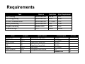
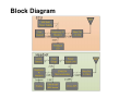
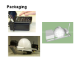
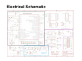
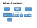
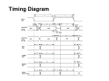
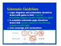
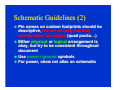
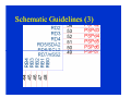
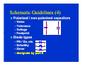
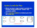
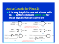
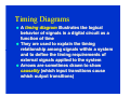
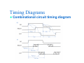
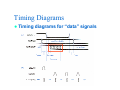
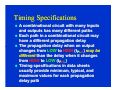
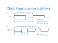
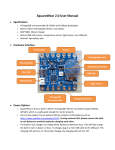
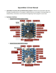
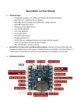
© 2014 by D. G. Meyer
ECE 477 Digital Systems
Senior Design Project
Module 7
Project Documentation Standards
Reference: Wakerly DDPP 4th ed
ed,, pp. 342342-370
Instructional Objectives:
To review the foundations of structured
digital system design
To review logic design documentation
standards
To review how to draw timing diagrams and
use timing specifications
Outline
Documentation standards
Guidelines
Electrical schematic homework
Documentation Standards
Good documentation is essential for correct
design and efficient maintenance
A documentation package should contain:
– abstract
– specifications/requirements
– block diagram
– packaging
– electrical schematic, narrative description
– PCB layout diagram, narrative description
– software organization, narrative description
– bill of materials
– timing diagram
– structured logic device description (HDL)
(HDL)
– user manual
Abstract
An Augmented Reality Simulator that allows
multiple users to interact in a mobile, outdoor
environment simulation. A central control unit
will coordinate the game play while per-player
headsets will appropriately overlay gameobject pixels on a semi-transparent panel that
is suspended in front of the users’ eyes. This
product is intended to be used for gaming and
other potential simulations that require an
augmented environment.
Specifications
The Augmented Reality Simulator consists of two
primary components: a single immotile central control
unit (CCU), and multiple per-user mobile headsets. A
user chooses the desired simulation (e.g. game or
virtual tour) via the CCU, which is equipped with a
keypad and LCD display. The CCU will then wirelessly
transmit all simulation-relevant data (e.g. 2D images,
3D models, and if the headsets were equipped with
speakers, audio files) to the headsets, which the CCU
will later reference by index. The CCU will then signal
the start of the simulation to the headsets, and then
coordinate game logic throughout the simulation by
taking into account the periodic sensor (IMU, GPS)
readings returned by each headset. Each headset will
also make use of its sensor readings by rendering the
image depending on user head orientation, geospatial
location, and status in the game/virtual tour.
Requirements
Task
IMU filtering
GPS string parsing
Wireless communication
Battery monitoring
Graphics rendering
Simulation logic
Device
External GPU
GPS
Battery Monitor
IMU
Wireless
Future Expansion
Peripheral
SPI
UART
I2C
I2C
UART
GPIO
Runs on
Microcontroller
Microcontroller
Microcontroller
Microcontroller
Headset GPU
CCU
Special Features
Master Mode, Chip Select
Open-Drain, Current Sink
Open-Drain, Current Sink
Full Duplex
Configurable Data Direction
Data Rate
800 Hz
20 Hz
11.5 KB/s
1 Hz
30 Hz
Varies
Jitter Requirement
5 us
None
1 ms
None
5 ms
Varies
Minimum Speed
800 KHz
115.2 Kbaud
400 KHz
400 KHz
115.2 Kbaud
N/A
Minimum Pins:
Pin Count
5
1
2
2
2
10
22
Block Diagram
Packaging
Electrical Schematic
Circuit Narrative
The augmented reality system comprises multiple battery-powered
headsets controlled by a microcontroller and one Raspberry Pi, and
a single central control unit controlled by one Raspberry Pi.
Upon insertion of a 3.7V lithium ion battery into the headset, or the
contact closure of the battery’s on/off switch, the battery’s voltage is
connected to the input of 4 power supplies, the input of the battery
“fuel gauge”, and the output of the battery charger. A polarized
battery header will be used to prevent the physical insertion of the
battery in the wrong polarity direction. The single battery powers all
components of the headset except for the battery charger, which is
optionally powered by an external 5V source in the form of a USB
connection. Three of the four power supplies are low dropout (LDO)
regulators which altogether supply 3.3V to the IMU sensors, GPS,
Raspberry Pi, microcontroller, and XBee radio. The fourth power
supply is integrated in the LCD package, and accepts the battery’s
3.7V directly. Once the IMU sensors are powered, they are capable
of transmitting raw sensor data to the microcontroller for processing
via I2C protocol [34]. The battery fuel gauge will similarly
communicate the battery’s charge to the microcontroller via I2C [22].
The Raspberry Pi will communicate with the microcontroller via SPI,
and both the GPS and XBee modules will communicate with the
microcontroller via the USART protocol [35, 6].
PCB Layout
PCB Narrative
Several of the components of this project, most notably the USB
boot loader described in the microcontroller datasheet, depend on a
stable clock source. Therefore, an external crystal oscillator in a
through-hole package was utilized with the recommended load
capacitance of 20pF [36]. As the traces leading to the crystal also
add impedance, the EAGLE “run length-freq-ri” tool was used to
match the oscillator trace lengths within 8mil. The crystal was also
placed as close as possible to the microcontroller while still allowing
a component-free area around the oscillator to limit noise coupling.
Similarly, the same method was used to match the USB data traces
to significantly less than the stated 50mil length tolerance [5].
Part placement near the microcontroller was also a major concern. In
order for the PCB to be physically possible to route, pin
assignments with multiple equivalent options on the microcontroller
were chosen to limit the number of crossing signals. Careful effort
was also spent in placing parts to minimize the number of traces
looping around the microcontroller and interfering with power
routing as shown in Figure 9.1. After placement was finalized, the
most convenient spare I/O pins were brought out to pads and a
spare serial port was connected to an unpopulated header for
debugging and future expansion. Two spare LEDs also aid in
debugging.
Software Organization
Software Narrative
Figure 10.5 shows the hierarchical arrangement of the various code
modules included in our design. The code modules in our design are: the
central control unit user interface, the central control unit simulation, the
headset main module, the headset GPS IRQ, the headset IMU IRQ, the
headset battery IRQ, the headset XBee IRQ, and the headset GPU.
The central control unit user interface is written in Python Tkinter [30].
Tkinter was chosen because a complex user interface is not needed, and
because the author is familiar with the software. The user interface
launches on startup of the central control unit and begins looking for
available headsets to join in simulations. The user is able to choose
available headsets and add them. The simulation allows a user to select a
simulation to run. After selecting a simulation, the rules and hazards are
explained to the user. The GUI will then launch the simulation and wait for
it to end.
The central control unit simulation will first load image and object data to
all headsets through wireless communication. It will then proceed to send
updates about the position of the image and object data to the user.
Updates about the headsets position will be periodically processed and
collision detection will be performed to determine simulation events to be
triggered. Due to limited accuracy of the GPS, virtual objects will be made
large (approximately 2 meters) for the purposes of detecting collisions.
Bill of Materials
Vendor
Digi-Key
Digi-Key
Digi-Key
Digi-Key
SparkFun
SparkFun
Adafruit
Newark
Newark
Newark
Micrel
Micrel
Maxim IC
Microchip
Manufacturer
SGS Thomson
Digi Corporation
Miscellaneous
SGS Thomson
OnShine
SkyTraq Technology
Unknown
Raspberry Pi
Foundation
Miscellaneous
L-Com
Micrel
Micrel
Maxim IC
Microchip
Part No.
STM32F405RGT6
XBee Pro 900HP S3B
N/A
STEVAL-MKI108V2
ANT-555
Venus 638FLPx
N/A
Model A
N/A
HG905RD-RSP
MIC5216
MIC5219
MAX17043
MCP73831
Description
Microcontroller
Wireless Communication Device
Passive components
Inertial Measurement Unit 9-DOF
GPS Antenna RP-SMA
Global Positioning System Receiver
Composite Input Display 4.3”
Central Control Unit Motherboard and
Headset GPU Motherboard
Wall Supply/SD cards for Raspberry Pi
Wireless Antenna
Regulator LDO 500mA MSOP-8
Regulator Low Noise LDO SOT-23-5
Voltage Based Battery Fuel Gauge
Linear Charge Management Controller
Unit Cost Qty
11.45 1
39.00 2
10.00 1
27.60 1
12.95 1
49.95 1
49.95 1
25.00 2
12.00
19.28
0.00
0.00
0.00
0.00
TOTAL
1
2
2
1
2
1
Total Cost
$11.45
$78.00
$10.00
$27.60
$12.95
$49.95
$49.95
$50.00
$12.00
$38.56
$0.00
$0.00
$0.00
$0.00
$340.46
Timing Diagram
User Manual
1.0 Illustration
1.0 Product Setup Instructions
•
Find a location to play:
o Find a location outside to play, preferably a big open field with a building nearby
that has an outlet on the outside. If necessary, acquire a long extension cord that
can stretch into the field.
•
Turn on the Devices:
o Plug the Central Control Unit in to turn it on. Flip the switch on the back of the
headset to turn it on as well. Wait until there is a red flashing light on the board in
the back of the headset. This indicates that the Global Positioning System is
ready.
•
Initial Configuration:
o Wait for a screen on the Central Control Unit that looks like the following:
Power Switch
o Press “Enter” on the numeric pad to continue to the next screen that looks like the
following:
1.
2.
3.
4.
Keypad – Use the keypad to interact with the Central Control Unit.
Screen – Use the screen to receive feedback from the Central Control Unit.
Antenna – The antenna is used to communicate with the headset. Do not remove.
Helmet – The helmet provides a secure mounting framework and comes with an
adjustable strap.
5. Display – The display projects the image seen on the reflector.
6. Reflector – Reflects the image from the display.
7. Antenna – The headset antenna is used to communicate with the Central Control Unit.
8. Charging port – Plug a USB cable in the charging port and the computer to charge the
headset’s battery. A battery charging LED will turn on.
9. Electronics Enclosure – The black box at the back of the headset containing the GPS
and other important electronic devices.
10. Power Switch – Turn power on for headset device.
o Wait for the Central Control Unit to detect a headset. If no headset is detected,
please refer to the troubleshooting section. When the Central Control Unit detects
a headset, press “0” to select the headset. Multiple headsets are not currently
supported. You may continue by pressing “Enter” on the numeric pad.
Guidelines
Schematics
Active levels for pins
Timing diagrams
Schematic Guidelines
Logic diagrams and schematics should be
drawn with gates in their “normal”
orientation (inputs on left, outputs on right)
A complete schematic page should be
drawn with system inputs on the left and
outputs on the right
Line crossings and connections
Schematic Guidelines (2)
Pin names on custom footprints should be
descriptive, but not so long that they
overlap other pin names (quad packs…)
Either physical or logical arrangement is
okay, but try to be consistent throughout
document
Use power / ground symbols
For power, show net alias on schematic
Schematic Guidelines (3)
Schematic Guidelines (4)
Polarized / nonnon-polarized capacitors
– Value
– Tolerance
– Voltage
– Footprint
Diode types
– PN / Ge
Ge,, etc.
– Schottky
– Zener
– designate by part #
+
Active Levels for Pins
When we draw a logic symbol, we think of a
function being performed “inside” that
symbolic outline
Use inversion bubbles to indicate pins that
are active low
Active Levels for Pins (2)
It is very helpful to use net aliases with
an _L suffix to indicate active low for
those signals that are active low
Timing Diagrams
A timing diagram illustrates the logical
behavior of signals in a digital circuit as a
function of time
They are used to explain the timing
relationship among signals within a system
and to define the timing requirements of
external signals applied to the system
Arrows are sometimes drawn to show
causality (which input transitions cause
which output transitions)
Timing Diagrams
Combinational circuit timing diagram
Timing Diagrams
Timing diagrams for “data” signals
Timing Specifications
A combinational circuit with many inputs
and outputs has many different paths
Each path in a combinational circuit may
have a different propagation delay
The propagation delay when an output
changes from LOW to HIGH (tPLH) may be
different than the delay when it changes
from HIGH to LOW (tPHL)
Timing specifications in data sheets
usually provide minimum, typical, and
maximum values for each propagation
delay path
Clock Signals (active high/low)
Timing Diagrams and Specifications
For synchronous systems, timing diagrams can be
used to show the relationship between the clock and
various input, output, and internal signals
clock frequency (f) = 1/tclk duty cycle = tH/(tH+tL)
time
low
time
high
flip--flop C→Q
flip
C→Q prop delay
clock
period
comb output prop delay
flip-flop setup and hold times
Electrical Schematic Homework
Theory of operation. Describe the function
and operating mode of each major
subsection of the circuit, as well as how the
subsections relate to each other. Discuss
the function and operating mode of major
components, including rationale for choice
of operating frequency, supply voltage(s),
etc, not rationale for the choice of the
component. Do not rehash the
manufacturers’ data sheets for the parts.
Tell us how the parts work in your circuit.
Electrical Schematic Homework
Hardware design narrative. Discuss which
subsystems of the microcontroller will be
used and how they will be used. Discuss
the port assignments of the microcontroller
and why specific ports were chosen for
specific functions. Include power, ground,
and bypass capacitor considerations. For
the other major subsystems, discuss any
specific configuration choices and how they
affect the interconnection between these
subsystems and the microcontroller.
Reference the schematic in this discussion.