1
Order this document
by AN1748/D
Freescale Semiconductor
Freescale Semiconductor, Inc...
AN1748
Building a Universal Serial Bus Keyboard Hub
Using the Motorola MC68HC(9)08KH12
By Patrick Keating
Product Engineer, Consumer Systems Group, Home Electronics
Austin, Texas
Introduction
The universal serial bus (USB) is changing the way in which computer
users plug in and activate computer peripheral devices. The “plug-nplay” or “hot swap” abilities of this peripheral bus architecture allow users
to plug in peripherals — such as keyboards — and immediately have
them available for use without rebooting the PC. No longer do users
have to suffer through the detangling of wires at the back of the PC,
configuring DIP switches, or even bothering with loading software
drivers.
USB is the evolution of the ISA and PCI computer serial bus. This
architecture will allow up to 127 peripherals to be plugged into a personal
computer using only two ports on the back of the PC. This is
accomplished through the daisy chaining of devices using “hubs,” which
allow users to link peripherals back to the host PC through other USB
devices which have extra downstream USB connections.
© Freescale Semiconductor, Inc., 2004. All rights reserved.
Motorola, Inc., 1998
AN1748
For More Information On This Product,
Go to: www.freescale.com
Freescale Semiconductor, Inc.
Application Note
The new serial bus standard, developed by computer industry leaders,
was made necessary by the increasing demands of greater PC
performance.
Freescale Semiconductor, Inc...
One of the classes of the USB is the human interface device (HID). HIDs
include devices such as mice, gamepads, and keyboards. Computers
today have incredible computing power which lends themselves to
telephony, audio/visual applications, and a wide range of HIDs. The
diversity of these potential HIDs also requires the USB to allow small,
periodic transfer operations for low-speed devices such as mice and
keyboards and isochronous operation for high-speed applications such
as telephony and audio.
Because these different types of devices require varying speed
performance and bandwidth, USB has capabilities for high-speed
devices that operate at 12 megabits per second (MBPS) and low-speed
devices that operate at 1.5 MBPS.
Additional hardware improvements that make USB a more desired way
of installing new peripherals include:
•
Unique USB connector design. Unlike previous connector
scenarios in which every peripheral had its own connector design
with a varying number of pins, USB uses two standard types of
connector:
– An upstream connector. See Figure 1 for a description of the
upstream connector.
– A downstream receptacle
•
The cable between the connectors can have two configurations,
depending upon the speed of the peripheral it is connecting:
– For high-speed devices, there is a power wire, a ground wire,
and two shielded signal wires that carry the USB data.
– For low-speed devices, the configuration is the same except
the signal wires are not shielded because they are less
sensitive to line noise.
AN1748
2
For More Information On This Product,
Go to: www.freescale.com
Freescale Semiconductor, Inc.
Application Note
Introduction
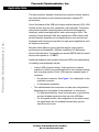
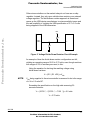
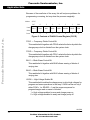
DIFFERENTIAL
SIGNAL PAIR
POWER PAIR
Freescale Semiconductor, Inc...
Figure 1. USB Connector with Pin Identification
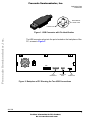
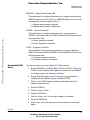
The USB connector plugs into the ports located on the backplane of the
PC, as seen in Figure 2.
USB
SCSI
INTERFACE
GRAPHICS
PORT
LAN
INTERFACE
Figure 2. Backplane of PC Showing the Two USB Connections
AN1748
3
For More Information On This Product,
Go to: www.freescale.com
Freescale Semiconductor, Inc.
Application Note
Freescale Semiconductor, Inc...
This application note:
NOTE:
•
Reviews the design of a legacy type keyboard and discusses
important features of the key scan algorithm
•
Is an overview of the MC68HC(9)08KH12 as well as a discussion
of the USB module operation
•
Describes the one high-speed, 12 MBPS, upstream port
connection and four high-speed (12 MBPS) or low-speed
(1.5 MBPS) downstream port connections
•
Explores the integrated 3.3-volt voltage regulator
•
In-depth instruction on the programming of the 12 Kbytes of
FLASH memory
•
Outlines the steps needed to construct a keyboard hub with
universal serial bus functionality using the Motorola 8-bit
MC68HC(9)08KH12 microcontroller
This application note assumes that the reader is familiar with the
Motorola HC08 Family of 8-bit microcontrollers and the universal serial
bus.
PS/2 Keyboard Design
The concept of the PS/2 keyboard design is founded in the combination
of a grid-like hardware setup and software that scans the grid, decoding
any interrupt to the specific key or keys that have been depressed.
Keyboards typically have from 101 to 104 keys. The keys are laid out in
X rows and Y columns, forming the grid which is easily decoded then by
the software to determine the keystroke. The number of columns is
typically eight, while the row count is between 18 and 20.
The “brains” of the keyboard are found in an 8-bit microcontroller that
takes the input from the keyboard, decodes it, then sends the
information to the host computer. This arrangement frees the
microprocessor of the PC from constantly polling the keyboard, relying
AN1748
4
For More Information On This Product,
Go to: www.freescale.com
Freescale Semiconductor, Inc.
Application Note
PS/2 Keyboard Design
instead upon the interrupts of the keyboard microcontroller to transfer
the information when it is inputted.
The Y columns of the grid are wired to microcontroller port pins that have
an internal pullup to VDD device as well as the ability to request an
interrupt. The interrupt request is active low, so applying a low to the pin
will pull the pin to ground, causing an interrupt request to occur.
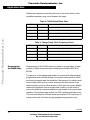
Freescale Semiconductor, Inc...
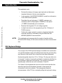
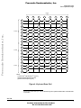
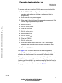
See Figure 3 for a physical description of how row and column pins are
tied together. See Figure 4 for an example of a keyboard scan grid.
KEY X, Y
Figure 3. Representation of Key and Resulting Row X,
Column Y Contact/Open
The operation of first determining if a key or keys has/have been
depressed and then decoding the information to send to the host
computer is:
1. All eight of the column port D pins are pulled high through an
internal pullup resistor. The keyboard interrupt pin also is enabled
for the eight column port pins.
2. The microcontroller software pulls down one of the row port pins
to ground while pulling up the remaining row port pins to VDD. For
example, if port A consists of port A0 through port A7, port B
consists of port B0 through port B4 and port C consists of port C0
through port C4, then port A0 will be pulled low and the remaining
17 row port pins will be pulled high.
3. If a key (or keys) is/are depressed in the row(s) that correspond(s)
to the port that is pulled low, then the associated column also will
be pulled low, because the row and column are now tied together
AN1748
5
For More Information On This Product,
Go to: www.freescale.com
Freescale Semiconductor, Inc.
Application Note
electrically by the depressed key as in Figure 3. This will cause a
keyboard interrupt for that column port pin. If no port D pins are
pulled low, that indicates that no key is depressed and the
software will continue to scan.
Freescale Semiconductor, Inc...
4. If a port D pin is pulled low and, therefore, requests an interrupt,
the software jumps to a subroutine that decodes the combination
of the row and column pins sending the value corresponding to the
x,y grid location to the host computer. Then the computer will
output the character to the monitor.
5. The microcontroller software then pulls the next row low, port A1,
and pulls the rest of the row pins high. The sequence continues
until all the rows are pulled low through port C4. The process of
alternately pulling all the row pins low takes approximately 12 ms.
Once port C4 is pulled low, the process starts over at port A0,
repeating the sequence.
AN1748
6
For More Information On This Product,
Go to: www.freescale.com
Freescale Semiconductor, Inc.
Application Note
PS/2 Keyboard Design
PORT D
D7
A0
D6
D5
D4
D3
D2
D1
S
CL
W
F1
2@
X
A1
LCt
A2
RCt
L⇑
A4
––>
2
A5
A6
A7
3pd
6––>
9pu
PU
PD
*
. De
––>
-
R⇑
5
8↑
Ins
F12
/
0In
––>
A3
D0
1en
4 <––
7H
Del
F11
NL
<––
Ent
Note
(3)
+
Hm
End
PB
↑
B
F
T
R
5%
4$
V
G
B0
D
F3
E
F2
3#
C
F4
B1
A
Tb
Q
‘~
1!
Z
Esc
M
H
Freescale Semiconductor, Inc...
PORT A
PORT B
B2
N
J
Y
U
6^
7&
B3
/?
;:
[{
P
-_
0)
K
]}
I
=+
8*
B4
‘“
,<
Note
(2)
C0
C1
PORT C
F6
C2
Spa
C3
RAI
C4
Note
(1)
L
F7
\|
Bsp
O
F8
9(
.>
F9
F10
↵
SL
PS
F5
LAI
Notes:
(1) Microsoft right Windows logo key
(2) Microsoft left Windows logo key
(3) Microsoft Notepad logo key
Figure 4. Keyboard Scan Grid
Microsoft, the Microsoft logo, and the Windows logo are registered trademarks of the Microsoft
Corporation.
AN1748
7
For More Information On This Product,
Go to: www.freescale.com
Freescale Semiconductor, Inc.
Application Note
Description of the MC68HC(9)08KH12
The MC68HC(9)08KH12 is a member of the low-cost, high-performance
68HC08 Family of 8-bit microcontrollers. This device is a fully compliant
USB 1.0 composite HUB microcontroller and is available in a 64-pin
quad flat pack (QFP) plastic package.
Freescale Semiconductor, Inc...
Additional features of the MC68HC(9)08KH12 include:
•
Five on-chip USB transceivers
•
On-chip 3.3-volt regulator for USB transceivers
•
1 x 12-MHz upstream USB port
•
4 x 12-MHz/1.5-MHz downstream USB ports
•
1 x hub control endpoint with:
– 8-byte transmit buffer
– 8-byte receive buffer
•
1 x hub interrupt endpoint:
– 1-byte transmit buffer
•
1 x device control endpoint:
– 8-byte transmit buffer
– 8-byte receive buffer
•
Device interrupt endpoints:
– 8-byte transmit buffer
•
384 bytes of RAM
•
12 Kbytes of FLASH memory with security
•
42 general-purpose input/output (I/O) ports, 29 of them with
software configurable pullups
•
16-bit, 2-channel timer interface module
•
20-bit keyboard interrupt port
•
Five LED (light emitting diode) direct drive port pins
•
COP (computer operating properly) reset counter
AN1748
8
For More Information On This Product,
Go to: www.freescale.com
Freescale Semiconductor, Inc.
Application Note
Universal Serial Bus Module
Universal Serial Bus Module
The MC68HC(9)08KH12 is designed to function as a compound device.
An embedded, full-speed device is combined with a hub in the single
USB module.
Freescale Semiconductor, Inc...
The hub is capable of performing these five basic properties controlled
by the hardware or software:
•
Connectivity behavior
•
Power management
•
Device connect/disconnect detection
•
Bus fault detection and recovery
•
Full/low-speed device support
For the embedded device submodule, three types of USB data transfer
are supported:
•
Control
•
Interrupt
•
Bulk, transmit only
The USB module is designed to be invisible to the end user. Simply plug
in the USB peripheral and it is immediately active and available, living up
to the “plug-n-play” promise.
The MC68HC(9)08KH12 differs from other Motorola USB
microcontrollers in that it has hub functionality. The keyboard
constructed with the MC68HC(9)08KH12 is capable of having up to four
high/low-speed peripherals plugged into it.
The microcontroller performs the functions of hub controller as well as
hub repeater, providing a path to the next USB device upstream and
then eventually to the host through the root port.
More generally, the hub must support the USB functionality
requirements.
AN1748
9
For More Information On This Product,
Go to: www.freescale.com
Freescale Semiconductor, Inc.
Application Note
Connectivity behavior of the hub varies, depending on whether it is
propagating traffic or resuming signaling or simply going into an idle
state. Power management involves the stopping or resuming of the
power supply to the device, depending on the user requirements. These
transitions conserve power consumption, making the device operation
more efficient.
Freescale Semiconductor, Inc...
The recognition of device connect or disconnect is an important function
of the hub controller. The connect detection occurs when a low- or highspeed device transitions the DMINUS or DPLUS line, respectively, high.
Both the DPLUS and DMINUS pins, when in a disconnected state, are
pulled low to ground through the 15-kΩ pulldown resistors. This signals
the USB host that there is not a device attached to that node. To discern
whether a high- or low-speed device has been attached to a node, the
hub controller determines which signal line, DPLUS or DMINUS, is
pulled up to the 3.3-volt USB operating voltage. If DPLUS is pulled up, it
is a high-speed device; DMINUS being pulled up to 3.3 volts indicates
that a low-speed device has been attached.
Because hubs are a main link in USB connectivity, it is essential that they
have the ability to sense possible errors and prevent them from
occurring, preserving the functionality of the connected network of USB
devices.
The last aspect of hub functionality, full/low speed device support, allows
the hub to be open for connectivity to any one of the numerous USB
devices available to the end user, both full and low speed. This feature
gives the hub maximum flexibility and usability.
The USB module contains an on-chip voltage regulator which is
essential to providing a 3.3-volt signal to the USB transceiver pins. The
on-board voltage regulator transitions the 5-volt VDD signal to the
required 3.3-volt USB transceiver voltage, eliminating the need for an
external voltage regulator.
The on-chip design eliminates the sensitivity to noise that is existent in
the USB device and virtually guarantees that the transceiver signals will
always be compliant to the 3.3 ± 0.3-volt USB specification.
AN1748
10
For More Information On This Product,
Go to: www.freescale.com
Freescale Semiconductor, Inc.
Application Note
Universal Serial Bus Module
Other microcontrollers on the market today do not have an on-chip
regulator. Instead, they rely upon a divide down resistor or an external
voltage regulator. The divide down resistor approach is flawed and
opens up the USB device manufacturer to noise sensitivity issues and
the real possibility of violating the USB specification of 3.3 ± 0.3 volts
being supplied to the USB transceiver.
Freescale Semiconductor, Inc...
VDD
R2
USB
CABLE
D1–
R1
Figure 5. Voltage Divide Down Resistor Circuit Example
An example of how the divide down resistor configuration can fail,
yielding an operating range of 2.83 to 3.79 volts, even though resistors
with ranges of 5% in accuracy are used, is this:
Using the equation for deriving the resulting voltage using
divide down resistors:
V = (R1 / (R1 +R2)) x VDD
NOTE:
VDD being supplied to the microcontroller is assumed to be in the range
of 4.4 to 5.5 volts DC.
Exceeding the specification on the high side assuming 5%
accurate resistors:
V = (15750 Ω / (15750 Ω + 7125 Ω)) x 5.5 volts
V = 3.79 volts
AN1748
11
For More Information On This Product,
Go to: www.freescale.com
Freescale Semiconductor, Inc.
Application Note
Exceeding the specification on the low side, again assuming
5% accurate resistors:
V = (14250 Ω / (14250 Ω + 7875 Ω)) x 4.4 volts
Freescale Semiconductor, Inc...
V = 2.83 volts
Both of these possible outcomes of the voltage divide down via the
resistors results in a violation of the USB specification. Using high
precision resistors can lower the chance of exceeding the specification,
but the additional cost, which can be a significant percentage of the
microcontroller cost, does not make this a reliable or cost-effective
solution. Utilizing an external voltage regulator also adds a large cost to
the application, since it can be a large percentage of the semiconductor
selling price.
The integrated voltage regulator of the MC68HC(9)08KH12 yields the
most robust performance, matched only by its highly competitive cost.
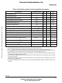
Port Pins
The MC68HC(9)08KH12 port pin design allows the user a wide variety
of possible configurations. Table 1 lists some of the possible
configurations using the 42 port pins.
Table 1. Listing of MC68HC(9)08KH12 Port Pin Features
Software
External
Configurable
Interrupt
Pullups
LED
Direct
Drive
Optical Number of
Interface Pins / Port
Comments
General-purpose I/O (GP I/O)
Port A
X
8
Port B
X
8
GP I/O
Port C
X
5
LED drive, GP I/O
8
Keyboard interrupt, GP I/O
5
Interface for optical mouse,
keyboard interrupt, GP I/O
8
Keyboard interrupt, GP I/O
X
Port D
X
* Port E
X (4 pins)
Port F
X
X
X (4 pins)
* Note:
Port E4 is a general-purpose I/O pin only.
AN1748
12
For More Information On This Product,
Go to: www.freescale.com
Freescale Semiconductor, Inc.
Freescale Semiconductor, Inc...
Application Note
FLASH Memory
All ports can function as bidirectional, general-purpose I/O pins. Ports A,
B, C, and F have software configurable pullups. Port C has the capability
to drive LEDs with 3-mA source and up to 10-mA current sink capability.
Ports D, E, and F are configurable to act as external interrupt pins. Port
pins E0–E3 have the capability of being configured to support an optical
interface which can be useful for an optical mouse application. As
mentioned previously, the typical keyboard uses eight port pins for
columns and 18 port pins for rows to generate the keyboard grid. This
configuration leaves 16 port pins available for applications decided by
the user. The versatility of the port pin configuration allows the user a
wide range of options in which to use the available port pins for added
peripheral functionality.
FLASH Memory
Unlike other USB chips available in the marketplace, the
MC68HC(9)08KH12 has an embedded FLASH memory array. The
12 Kbytes of FLASH memory allow for lower cost application
development as well as easy in-circuit reprogramming to correct bugs or
update code that may exist in the application. The FLASH memory can
be read, programmed, and erased using a single external supply and an
on-board charge pump. The FLASH memory also has the Motorola
security feature which discourages others from accessing the
application code unless authorized by the code developers.
Additional features include a block protect register that will prevent
accidental overwrite or erase of programmed memory and a FLASH
control register that allows the user to specify whether a block, a page,
or the entire array can be erased.
There are also charge pump clock frequency select bits, a high-voltage
enable bit, and program/erase bits. (See Figure 6.) The internal charge
pump is designed to operate at the greatest efficiency in the frequency
range between 2 and 3 MHz.
Because the internal bus frequency is 1.5 MHz for the
MC68HC(9)08KH12 and there is no PLL (phase-locked loop) attached
to the charge pump, the charge pump must operate at 1.5 MHz ± 10%.
AN1748
13
For More Information On This Product,
Go to: www.freescale.com
Freescale Semiconductor, Inc.
Application Note
Because of the small size of the array, this will not pose problems for
programming or erasing, but may slow the process marginally.
Address:
Read:
Write:
Reset:
$FE07
Bit 7
6
5
4
3
2
1
Bit 0
FDIV1
FDIV0
BLK1
BLK0
HVEN
MARGIN
ERASE
PGM
0
0
0
0
0
0
0
0
Freescale Semiconductor, Inc...
Figure 6. Contents of FLASH Control Register (FLCR)
FDIV1 — Frequency Divide Control Bit
This read/write bit together with FDIV0 selects the factor by which the
charge pump clock is divided from the system clock.
FDIV0 — Frequency Divide Control Bit
This read/write bit together with FDIV1 selects the factor by which the
charge pump clock is divided from the system clock.
BLK1 — Block Erase Control Bit
This read/write bit together with BLK0 allows erasing of blocks of
varying size.
BLK0 — Block Erase Control Bit
This read/write bit together with BLK1 allows erasing of blocks of
varying size.
HVEN — High-Voltage Enable Bit
This read/write bit enables the charge pump to drive high voltages for
program and erase operations in the array. HVEN can be set only if
either PGM = 1 or ERASE = 1 and the proper sequence for
program/margin read or erase is followed.
1 = High voltage enabled to array and charge pump on
0 = High voltage disabled to array and charge pump off
AN1748
14
For More Information On This Product,
Go to: www.freescale.com
Freescale Semiconductor, Inc.
Application Note
FLASH Memory
MARGIN — Margin Read Control Bit
This read/write bit configures the memory for margin read operation.
MARGIN cannot be set if HVEN = 1. MARGIN will return to unset (0)
automatically if asserted when HVEN = 1.
1 = Margin read operation selected
0 = Margin read operation unselected
Freescale Semiconductor, Inc...
ERASE — Erase Control Bit
This read/write bit configures the memory for erase operation.
ERASE is interlocked with the PGM bit such that both bits cannot be
set at the same time.
1 = Erase operation selected
0 = Erase operation unselected
PGM — Program Control Bit
This read/write bit configures the memory for program operation.
PGM is interlocked with the ERASE bit such that both bits cannot be
set at the same time.
1 = Program operation selected
0 = Program operation unselected
Erasing the FLASH
Array
Use this procedure to erase a block of FLASH memory:
1. Set the ERASE bit, the BLK0, BLK1, FDIV0, and FDIV1 bits in the
FLASH control register. See Table 2 for block sizes and Table 3
for charge pump clock frequency settings.
2. Ensure that the target portion of the array is unprotected by
reading the block protect register, address $FF8D.
3. Write to any FLASH address with any data within the block
address range desired.
4. Set the HVEN bit.
5. Wait for a time, tERASE.
6. Clear the HVEN bit.
7. Wait for a time, tKILL, for the high voltages to dissipate.
8. Clear the ERASE bit.
9. After a time, tHVD, the memory can be accessed in read mode
again.
AN1748
15
For More Information On This Product,
Go to: www.freescale.com
Freescale Semiconductor, Inc.
Application Note
While these operations must be performed in the order shown, other
unrelated operations may occur between the steps.
Freescale Semiconductor, Inc...
Table 2. FLASH Erase Block Sizes
BLK1
BLK0
Block Size
0
0
Full array: 12 Kbytes
0
1
Half array: 6 Kbytes
1
0
Eight rows: 256 bytes
1
1
Single row (page): 32 bytes
Table 3. Charge Pump Clock Frequency Select
Programming
the FLASH Array
FDIV1
FDIV0
Pump Clock Frequency
0
0
Bus frequency ÷ 1
0
1
Bus frequency ÷ 2
1
0
Bus frequency ÷ 2
1
1
Bus frequency ÷ 4
Programming of the FLASH memory is done on a page basis. A page
consists of eight consecutive bytes starting from address $XXX0 or
$XXX8.
The purpose of the margin read mode is to ensure that data has been
programmed with sufficient margin for long-term data retention. While
performing a margin read, the operation is the same as for ordinary read
mode except that a built-in counter stretches the data access for an
additional eight cycles to allow sensing of the lower cell current. Margin
read mode imposes a more stringent read condition on the bitcell to
ensure the bitcell is programmed with enough margin for long-term data
retention. During these eight cycles, the COP counter continues to run.
The user must account for these extra cycles within COP feed loops. A
margin read cycle can follow a page programming operation only.
AN1748
16
For More Information On This Product,
Go to: www.freescale.com
Freescale Semiconductor, Inc.
Application Note
FLASH Memory
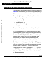
To program and margin read the FLASH memory, use this algorithm:
1. Set the PGM bit. This configures the memory for program
operation and enables the latching of address and data for
programming.
2. Read from the block protect register.
3. Write data to the eight bytes of the page being programmed. This
requires eight separate write operations.
Freescale Semiconductor, Inc...
4. Set the HVEN bit.
5. Wait for a time, tPROG.
6. Clear the HVEN bit.
7. Wait for a time, tHVTV.
8. Set the MARGIN bit.
9. Wait for a time, tVTP.
10. Clear the PGM bit.
11. Wait for a time, tHVD.
12. Read back data in margin read mode. This is done in eight
separate read operations which are each stretched by eight
cycles.
13. Clear the MARGIN bit.
See Figure 7 for a flowchart describing the smart programming
algorithm. The assumptions made for the page program/margin read
procedure are that the page to be programmed is already erased.
This program/margin read sequence is repeated throughout the memory
until all data is programmed. For minimum overall programming time and
least program disturb effect, the smart programming algorithm must be
followed. The associated specification limits of the parameters listed in
the program and erase routines are listed in Table 4.
AN1748
17
For More Information On This Product,
Go to: www.freescale.com
Freescale Semiconductor, Inc.
Application Note
PROGRAM FLASH
INITIALIZE ATTEMPT COUNTER TO 0
SET PGM BIT AND FDIV BITS
READ FLASH BLOCK PROTECT REGISTER
Freescale Semiconductor, Inc...
WRITE DATA TO SELECTED PAGE
SET HVEN BIT
WAIT t Step
CLEAR HVEN BIT
WAIT t HVTV
SET MARGIN BIT
WAIT t VTP
CLEAR PGM BIT
WAIT t HVD
MARGIN READ PAGE OF DATA
CLEAR MARGIN BIT
INCREMENT ATTEMPT COUNTER
NO
ATTEMPT COUNT
EQUAL TO
flsPulses
?
YES
PROGRAMMING OPERATION
FAILED
NO
MARGIN READ DATA
EQUAL TO
WRITE DATA
?
YES
PROGRAMMING OPERATION
COMPLETE
Figure 7. Smart Programming Algorithm for FLASH Memory
AN1748
18
For More Information On This Product,
Go to: www.freescale.com
Freescale Semiconductor, Inc.
Application Note
FLASH Memory
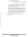
Table 4. Specification Limits for the Program/Erase Parameters
Freescale Semiconductor, Inc...
Characteristic
Symbol/Description
Min
Max
Units
FLASH pages per row
—
8
8
Pages
FLASH bytes per page
—
8
8
Bytes
FLASH read bus clock frequency
tRead(1)
32 k
8.4 M
Hz
FLASH charge pump clock frequency
tPump(2)
1.8
2.3
MHz
FLASH block/bulk erase time
tErase
100
—
ms
FLASH high voltage kill time
tKill
200
—
µs
FLASH return to read time
tHVD
50
—
µs
FLASH page program time
flsPulses(3)
—
30
Pulses
FLASH page program step size
tStep(4)
1.0
1.2
ms
FLASH HVEN low to margin high time
tHVTV
50
—
µs
FLASH margin high to PGM low time
tVTP
150
—
µs
tRecovery(5)
500
—
Dummy
read cycles
FLASH row erase endurance(6)
—
100
—
Cycles
FLASH row program endurance(7)
—
100
—
Cycles
FLASH data retention time(8)
—
10
—
Years
FLASH return to read after margin read time
Notes:
1. tRead is defined as the frequency range for which the FLASH memory can be read.
2. tPump is defined as the charge pump frequency required for program, erase, and margin read operations.
3. flsPulses is defined as the number of pulses used during FLASH programming required by the smart program algorithm.
4. tStep is defined as the amount of time during one page program cycle that HVEN is held high.
5. tRecoveryis defined as the minimum number of dummy reads of any FLASH location before accurate data is read from
the memory after margin read mode is used.
6. The minimum row erase endurance value specifies each row of the FLASH memory is guaranteed to work for at least
this many erase cycles.
7. The minimum row program endurance value specifies each row of the FLASH memory is guaranteed to work for at
least this many program cycles.
8. The FLASH is guaranteed to retain data over the entire specified temperature range for at least the minimum time
specified.
AN1748
19
For More Information On This Product,
Go to: www.freescale.com
Freescale Semiconductor, Inc.
Application Note
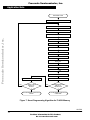
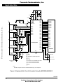
USB Keyboard Hub Design Using the MC68HC(9)08KH12
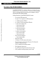
The keyboard hub design using the MC68HC(9)08KH12 is displayed in
Figure 8. As can be seen, the clock circuit is constructed using a total of
seven external components, five for the crystal oscillator and two for the
PLL.
Freescale Semiconductor, Inc...
The crystal oscillator is connected in the standard Pierce oscillator
configuration. The oscillator components include:
•
Fixed capacitor, C1
•
Tuning capacitor, C2
•
Feedback resistor, RB
•
Optional series resistor, RS
•
Crystal, X1
The values for these components are dependent upon the crystal
manufacturers’ specifications.
RS is drawn to match the Pierce oscillator requirements, but may be
removed depending upon the clock frequency. At higher frequencies,
the value of RS may be 0 or shorted. A low-cost, 6-MHz crystal provides
the clock to the MC68HC(9)08KH12. The PLL is present in the chip
design so that the 48-MHz and 12-MHz clock frequencies can be
provided to the USB module, supporting the high-speed USB
requirements of the upstream port and the potential high-speed
peripherals connected to the four downstream ports.
The keyboard scan matrix, as described earlier for the PS2 type
keyboard design, occupies 26 of the port pins. The keyboard LEDs for
Num Lock, Caps Lock, and Scroll Lock utilize three of the port C pins,
which are capable of sinking up to 10 mA of LED drive current.
The one upstream port, which is composed of VDDREGOUT, DPLUS0,
and DMINUS0, is configured with DPLUS0 pulled up to the 3.3-volt
signal, provided from VDDREGOUT by a 1.5-kΩ resistor, are also wired to
the upstream USB connector which provides the path back to the host
for the downstream ports.
AN1748
20
For More Information On This Product,
Go to: www.freescale.com
Freescale Semiconductor, Inc.
Application Note
USB Keyboard Hub Design Using the MC68HC(9)08KH12
The four downstream ports – D1, D2, D3, and D4 – all have the 15-kΩ
pulldown resistors attached, pulling them low when the USB lines go
idle. The transceiver pins are also wired to the female end of the USB
connector providing the hub connections.
Notice that there is no indication whether the downstream ports are high
or low speed as they are drawn in Figure 8. The determination of the
speed of the attached device is made within the attached device itself.
Freescale Semiconductor, Inc...
The USB peripheral connected to the individual downstream ports will
have the 1.5-kΩ pullup resistor to the USB operating voltage, 3.3 volts,
attached to the appropriate transceiver pin. It will be attached to DPLUS
for a high speed device and DMINUS for a low-speed device.
NOTE:
All power/ground (VDD/VSS) pairs should be isolated via a 10-nF
capacitor per pair.
AN1748
21
For More Information On This Product,
Go to: www.freescale.com
Freescale Semiconductor, Inc.
Application Note
C2
C1
X1
CBYP
CF
*RS
VDD
VDD
C3
Freescale Semiconductor, Inc...
1
2
3
4
VPP
C4
R1
UPSTREAM
PORT 0
R2
R2
R2
R2
1
DPLUS1
2
DMINUS1
3
4
DOWNSTREAM
PORT 1
1
DPLUS2
2
DMINUS2
3
4
DOWNSTREAM
PORT 2
DOWNSTREAM
PORT 3
1
DPLUS4
2
DMINUS4
3
4
DPLUS0
DMINUS0
DPLUS1
DMINUS1
DPLUS2
DMINUS2
DPLUS3
DMINUS3
DPLUS4
DMINUS4
MC68HC(9)08KH12
R2
R2
1
DPLUS3
2
DMINUS3
3
4
DOWNSTREAM
PORT 4
VDDA CGM- VSSA OSC2
XFC
VPP/IRQB
VDDREGOUT
DPLUS0
DMINUS0
RB
OSC1
PTD0
PTD1
PTD2
PTD3
PTD4
PTD5
PTD6
PTD7
COLUMN 1
COLUMN 2
COLUMN 3
COLUMN 4
COLUMN 5
COLUMN 6
COLUMN 7
COLUMN 8
PTA0
PTA1
PTA2
PTA3
PTA4
PTA5
PTA6
PTA7
ROW 1
ROW 2
ROW 3
ROW 4
ROW 5
ROW 6
ROW 7
ROW 8
PTB0
PTB1
PTB2
PTB3
PTB4
ROW 9
ROW 10
ROW 11
ROW 12
ROW 13
PTC0
PTC1
PTC2
PTC3
PTC4
PTC5
PTC6
PTC7
ROW 14
ROW 15
ROW 16
ROW 17
ROW 18
KEYBOARD
RST
R2
R2
X1 = 6 MHz
RB = 10 MΩ
*RS = OPTIONAL AT HIGHER FREQUENCY
R1 = 1.5 kΩ
R2 = 15 kΩ
CBYP = 10 nF
CF = CONSULT CRYSTAL VENDOR DATA SHEET
C1 = 2 X CRYSTAL LOAD CAPACITANCE
C2 = 2 X CRYSTAL LOAD CAPACITANCE
C3 = 1 µF
C4 = 0.1 µF
NUM LOCK
CAPS LOCK
SCROLL LOCK
VDD
Note:
All VDD / VSS pairs not shown should be isolated using 10-nF capacitors.
Figure 8. Keyboard Hub Circuit Schematic Using the MC68HC(9)08KH12
AN1748
22
For More Information On This Product,
Go to: www.freescale.com
Freescale Semiconductor, Inc.
Application Note
Firmware for the MC68HC(9)08KH12
Firmware for the MC68HC(9)08KH12
Freescale Semiconductor, Inc...
Code development can be arduous for the peripheral manufacturer with
limited resources and lack of experience with the requirements set forth
for USB devices.
Motorola has developed a scalable USB firmware code library to make
the transition from legacy type peripherals less painful and to reduce
development times significantly. The firmware library takes care of many
USB compatibility matters, providing USB conformant functions that
perform many of the required operations. Utilizing this library can cut
from two to three months off code development time, accelerating the
time to market for new USB peripherals.
This firmware library can be acquired from Motorola by contacting the
local Motorola representative for details.
Conclusion
The MC68HC(9)08KH12 is a well-integrated, robust, and versatile part
for peripheral manufacturers who are designing a USB keyboard with
high/low speed hub capability.
Additional features of the microcontroller include the integrated 3.3-volt
voltage regulator, which guarantees that the voltage source to the USB
module stays within specifications.
The Motorola USB firmware library is available for fast code
development and is fully scalable to the application for which it will be
used. Additional information for the firmware library and example
applications in which the MC68HC(9)08KH12 has been used can be
attained by contacting your local Motorola representative.
AN1748
23
For More Information On This Product,
Go to: www.freescale.com
Freescale Semiconductor, Inc.
R E Q U I R E D
Application Note
References
Universal Serial Bus Specification, Jan.15, 1996.
Motorola USB Firmware Library User’s Manual, Preliminary, Motorola.
October 1997.
How to Reach Us:
N O N - D I S C L O S U R E
Freescale Semiconductor, Inc...
A G R E E M E N T
Home Page:
www.freescale.com
E-mail:
[email protected]
USA/Europe or Locations Not Listed:
Freescale Semiconductor
Technical Information Center, CH370
1300 N. Alma School Road
Chandler, Arizona 85224
+1-800-521-6274 or +1-480-768-2130
[email protected]
Europe, Middle East, and Africa:
Freescale Halbleiter Deutschland GmbH
Technical Information Center
Schatzbogen 7
81829 Muenchen, Germany
+44 1296 380 456 (English)
+46 8 52200080 (English)
+49 89 92103 559 (German)
+33 1 69 35 48 48 (French)
[email protected]
Japan:
Freescale Semiconductor Japan Ltd.
Headquarters
ARCO Tower 15F
1-8-1, Shimo-Meguro, Meguro-ku,
Tokyo 153-0064
Japan
0120 191014 or +81 3 5437 9125
[email protected]
Asia/Pacific:
Freescale Semiconductor Hong Kong Ltd.
Technical Information Center
2 Dai King Street
Tai Po Industrial Estate
Tai Po, N.T., Hong Kong
+800 2666 8080
[email protected]
For Literature Requests Only:
Freescale Semiconductor Literature Distribution Center
P.O. Box 5405
Denver, Colorado 80217
1-800-441-2447 or 303-675-2140
Fax: 303-675-2150
[email protected]
Information in this document is provided solely to enable system and software
implementers to use Freescale Semiconductor products. There are no express or
implied copyright licenses granted hereunder to design or fabricate any integrated
circuits or integrated circuits based on the information in this document.
Freescale Semiconductor reserves the right to make changes without further notice to
any products herein. Freescale Semiconductor makes no warranty, representation or
guarantee regarding the suitability of its products for any particular purpose, nor does
Freescale Semiconductor assume any liability arising out of the application or use of
any product or circuit, and specifically disclaims any and all liability, including without
limitation consequential or incidental damages. “Typical” parameters which may be
provided in Freescale Semiconductor data sheets and/or specifications can and do
vary in different applications and actual performance may vary over time. All operating
parameters, including “Typicals” must be validated for each customer application by
customer’s technical experts. Freescale Semiconductor does not convey any license
under its patent rights nor the rights of others. Freescale Semiconductor products are
not designed, intended, or authorized for use as components in systems intended for
surgical implant into the body, or other applications intended to support or sustain life,
or for any other application in which the failure of the Freescale Semiconductor product
could create a situation where personal injury or death may occur. Should Buyer
purchase or use Freescale Semiconductor products for any such unintended or
unauthorized application, Buyer shall indemnify and hold Freescale Semiconductor
and its officers, employees, subsidiaries, affiliates, and distributors harmless against all
claims, costs, damages, and expenses, and reasonable attorney fees arising out of,
directly or indirectly, any claim of personal injury or death associated with such
unintended or unauthorized use, even if such claim alleges that Freescale
Semiconductor was negligent regarding the design or manufacture of the part.
For More Information On This Product,
Go to: www.freescale.com