1
SPACE 3D CAPACITANCE EXTRACTION
USER’S MANUAL
A.J. van Genderen, N.P. van der Meijs
Circuits and Systems Group
Department of Electrical Engineering
Delft University of Technology
The Netherlands
Report ET-NT 94.37
Copyright © 1994-2013 by the authors.
All rights reserved.
Last revision:
Januari 8, 2013.
Space 3D Capacitance Extraction
1
1. Introduction
1.1 3D Capacitance Extraction
Parasitic capacitances of interconnects in integrated circuits become more important as
the feature sizes on the circuits are decreased and the area of the circuit is unchanged or
increased. For submicron integrated circuits - where the vertical dimensions of the wires
are in the same order of magnitude as their minimum horizontal dimensions - 3D
numerical techniques are even required to accurately compute the values of the
interconnect capacitances.
This document describes the layout-to-circuit extraction program space3d, that is used to
accurately and efficiently compute 3D interconnect capacitances of integrated circuits
based upon their mask layout description. The 3D capacitances are part of an output
circuit together with other circuit components like transistors and resistances. This
circuit can directly be used as input for a circuit simulator like SPICE.
1.2 Space Characteristics
To compute 3D interconnect capacitances, space3d uses a boundary-element method. In
the boundary-element method, elements are placed on the boundaries of the
interconnects. This has as an advantage over the finite-element and the finite-difference
method (where the domain between the conductors is discretized) that - especially for 3D
situations - a lower number of discretization elements is used. However, a disadvantage
of the boundary-element method is that in order to compute the capacitance matrix it
requires the inversion of a full matrix of size N × N , where N is the total number of
elements. This takes O(N 3 ) time and O(N 2 ) memory.
To reduce the complexity of the above problem, space3d employs a new matrix inversion
technique that computes only an approximate inverse. In practice, this means that only
coupling effects are computed between ‘‘nearby’’ elements and that no coupling
capacitances are found between elements that are far apart. For flat layout descriptions,
this method has a computation complexity that is O(N ) and a space complexity that is
O(1). As a result, space3d is capable of quickly extracting relatively large circuits (> 100
transistors), and memory limitations of the computer are seldom an insurmountable
obstacle in using the program.
1.3 Documentation
Throughout this document it is assumed that the reader is familiar with the usage of space
as a basic layout-to-circuit extractor, i.e. extraction of transistors and connectivity. This
document only describes the additional information that is necessary to use space3d for
The Nelsis IC Design System
Space 3D Capacitance Extraction
2
3D capacitance extraction. The usage of space or space3d as a basic layout-to-circuit
extractor is described in the following documents:
•
Space User’s Manual
This document describes all features of space except for the 3D capacitance
extraction mode. It is not an introduction to space for novice users, those are
referred to the Space Tutorial.
•
Space Tutorial
The Space Tutorial provides a hands-on introduction to using space and the
auxiliary tools in the system that are used in conjunction with space. It contains
several examples.
•
Space Tutorial - Helios Version
The same tutorial as above, but now described under the assumption that the
graphical user interface helios is used to run the extraction tools.
•
Manual Pages
For space and space3d as well as for other tools that are used in conjunction with
space, manual pages are available describing (the usage of) these programs. The
manual pages are on-line available, as well as in printed form. The on-line
information can be obtained using the icdman program.
•
Xspace User’s Manual
This manual describes the usage of Xspace, a graphical X Windows based
interactive visualization tool of space3d. ( Xspace is also part of helios and can
best be run from there.)
Also available:
•
Space Substrate Resistance Extraction User’s Manual
This manual describes how resistances between substrate terminals are computed
in order to model substrate coupling effects in analog and mixed digital/analog
circuits.
1.4 On-line Examples
Two examples are presented in this manual that are also available on-line. We will
assume that the Space Software has been installed under the directory /usr/cacd. The
examples are then found in the directories /usr/cacd/share/demo/poly5 and
/usr/cacd/share/demo/sram respectively.
The Nelsis IC Design System
Space 3D Capacitance Extraction
3
2. Program Usage
2.1 General
3D capacitance extraction can be performed using one of the following versions of the
Space Software: space3d (for batch mode extraction) and Xspace (for interactive
extraction and mesh visualization). Both these tools can also be used from within the
graphical user interface helios.
Normally, when performing a 3D capacitance extraction, a flat extraction will be
executed. This implication can be disabled when turning on the parameter
allow_hierarchical_cap3d.
2.2 Batch Mode Extraction
In order to use the 3D capacitance extraction mode of space3d, use the option -3. Also,
use either the option -c or the option -C. In both cases, 3D ground and coupling
capacitances are computed. However, only in the second case all these capacitances will
be part of the output circuit. In the first case, all coupling capacitances will be
reconnected to ground.
2.3 Interactive Extraction
For 3D capacitance extraction it may be helpful to use the Xspace visualization program.
This program is not more an interactive version of the space3d program. But it runs
space3d in batch mode for each new extraction. It is using a "display.out" file to show the
results. The Xspace program runs under X Windows and uses a graphical window to,
among other things, show the 3D mesh that is generated by the program. Interactively,
the user can select the cell that is extracted, the options that are used, and the items that
are displayed. However, for a complete graphical interface to all extraction tools, it is
better to use the graphical user interface helios that includes space3d as well as Xspace.
For 3D capacitance extraction using Xspace, turn on "3D capacitance" and either
"coupling cap" or "capacitance" in the menu "Options". To display also the 3D mesh,
click on "DrawBEMesh" and "3 dimensional" (and possibly "DrawGreen") in the menu
"Display". Then, after selecting the name of the cell in the menu "Database", the
extraction can be started by clicking on "extract" in the menu "Extract".
To preview the mesh for 3D capacitance computation, use Xspace as described above and
also turn on "BE mesh only".
The Nelsis IC Design System
4
Space 3D Capacitance Extraction
3. Technology Description
3.1 Introduction
For 3D extraction, the space element definition file is extended with a description of the
vertical dimensions of the conductors, optionally, a description of the edge shapes of the
conductors, and a description of the dielectric structure of the circuit. Information about
these specifications is given below. For basic information about the development of an
element definition file (technology file), see the Space User’s Manual.
3.2 Unit Specification
Optionally the unit for distances in the vertical dimension list and the unit for distances in
the shape lists are specified in the unit specification of the element definition file. A unit
for the vertical dimension list is specified by means of the keywords unit and vdimension,
followed by the value of the unit. A unit for the edge/cross-over shape list is specified by
means of the keywords unit and shape, followed by the value of the unit.
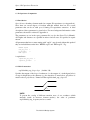
Example:
The following specifies a unit of 1 micron for distances that are given in the vertical
dimension list and for distances that are given in a shape list:
unit vdimension
unit shape
1e-6
1e-6
# micron
# micron
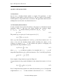
3.3 The Vertical Dimension List
Syntax:
vdimensions :
name : condition_list(s) : mask : bottom thickness
.
.
[ skip_cap3d : name1 name2 [: capacitivity] ]
[ keep_cap2d : cap2d-name ]
The vertical dimension list specifies for different conductors under different conditions
(e.g. metal2 above polysilicon or metal2 above metal1) (1) bottom: the distance between
the substrate and the bottom of the conductor (2) thickness: the thickness of the
conductor. The vertical dimension list is included in the element definition file after the
specification of the standard (non-3D) elements (see the Space User’s Manual).
Optional "skip_cap3d" can be specified for partial 2D surface capacitance extraction
between the specified two vdimension names. This is especial useful for large conductor
The Nelsis IC Design System
5
Space 3D Capacitance Extraction
plates and plates which lay very close to each other. The to use 2D surface capacitivity
value can be specified. A zero value skips the surface capacitance completely. Default
the value is calculated from the dielectric structure.
The "keep_cap2d" option can be specified for each 2D capacitance you want to keep
during 3D capacitance extraction.
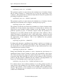
Example:
An example of an almost minimal technology file (with corresponding geometry) is
given below. While minimal, this file can actually be complete (except for a
specification of the dielectric structure) for 3D extraction for a double metal
process in which only metal1 and metal2 capacitances are extracted.
unit vdimension
1e-6
# micron
conductors :
metal1 : in : in : 0
metal2 : ins : ins : 0
vdimensions :
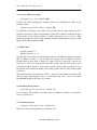
metal1_shape : in : in : 1.6 1.0
metal2_shape : ins : ins : 3.3 1.2
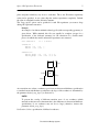
ins
1.0 µ
1.2 µ
in
3.3 µ
1.6 µ
At a transition area, where a conductor goes from one bottom and thickness specification
to another bottom and thickness specification, the slope of the conductor is determined by
the parameter default_step_slope (see Section 4.2).
NOTE:
To prevent the overlap of different transition areas of one conductor (which
currently results incorrect element meshes), the differences in bottom and thickness
specifications of one conductor may not be too large (otherwise: increase the
parameter default_step_slope).
See Section 3.8 for a specification of diffused conductors.
The Nelsis IC Design System
6
Space 3D Capacitance Extraction
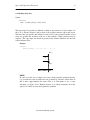
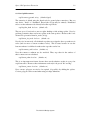
3.4 The Edge Shape List
Syntax:
eshapes :
name : condition_list(s) : mask : db dt
.
.
The edge shape list specifies for different conductors, the extension of each conductor in
the x (or y) direction relative to the position of the original conductor edge in the layout.
The first value (db) specifies the extension of the bottom of the conductor and the second
value (dt) specifies the extension of the top of the conductor. Either extension may be
negative. The edge shape list should be present in the element definition file after the
vertical dimension list.
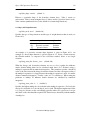
Example:
eshapes :
metal1_eshape : !in -in : in : 0.2 0.1
0.1 µ
in
0.2 µ
NOTE:
In some cases, the use of eshapes may cause mesh generation problems because
e.g. at corners the order of mesh nodes can get mixed up. Because of that, when db
and dt have (approximately) the same value, it is often better to use a resize
statement (see Space User’s Manual) instead of an eshape statement, since this
option is less likely to cause mesh generation problems.
The Nelsis IC Design System
7
Space 3D Capacitance Extraction
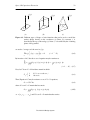
3.5 The Cross-over Shape List
Syntax:
cshapes :
name : condition_list(s) : mask : db1 dt1 db2 dt2
.
.
The cross-over shape list specifies for different conductors, the extensions of the bottom
and top of each conductor in the x (or y) direction relative to the position of a transition
edge in the layout. The transition edge, is an edge (caused by another mask), where a
conductor goes from one bottom and thickness specification to another bottom and/or
thickness specification. Thus, there must be two vdimension specifications for the same
conductor. The cross-over shape specification overrules the default_step_slope method
(see Section 4.2).
*
*
dt2
*
t2
dt2
t1
*
t2
dt2
* transition edge
dt2
t1
TOP
dt1
dt1
dt1
dt1
default: dt2 = 0 dt1 = (t2 − t1) / default_step_slope
db2
db1
db1
db1
b2
*
b1
BOTTOM
db2
db2
db1
*
b2
*
*
b1
default: db2 = 0 db1 = (b2 − b1) / default_step_slope
Note that the first and third value (db1 and db2) specify the extension of the bottom of the
conductor (at left and right side of the transition, db1 to b1 the lowest bottom value) and
the second and fourth value (dt1 and dt2) specify the extension of the top of the
conductor. Each extension value can may be negative. But be warned, some extension
combinations can result in an incorrect mesh. The cross-over shape list should be present
in the element definition file after the edge shape list.
Example:
vdimensions :
ver_cpg_of_caa : cpg !caa
ver_cpg_on_caa : cpg caa
# bottom thickness
: cpg : 1.6 0.5
: cpg : 1.8 0.4
cshapes :
cpg_cshape : cpg !caa -caa : cpg : 0.1 0.1 0.1 0.0
The Nelsis IC Design System
Space 3D Capacitance Extraction
8
3.6 Dielectric Structure
Syntax:
dielectrics :
name permittivity bottom
.
.
Specifies the dielectric structure of the chip. This specification is included in the element
definition file after the vertical dimension list and the shape lists. For each layer, name is
an arbitrary label that will be used for error messages etc, permittivity is a real number
giving the relative dielectric constant, and bottom specifies (in microns) the bottom of the
dielectric layer. The value of bottom must be ≥ 0. The first dielectric in the list specifies
the lowest dielectric, the second dielectric the second lowest, etc. For the first dielectric
layer bottom must be zero. The top of a dielectric layer is at the bottom of the next
dielectric. The top of the last dielectric is at infinity. No dielectric layers means vacuum.
If one or more dielectric layers are specified, a ground plane at zero is present.
Example:
dielectrics :
# Dielectric
# (epsilon =
SiO2
3.9
air
1.0
consists of 5 micron thick SiO2
3.9) on a conducting plane.
0.0
5.0
NOTE:
If more than 3 dielectric layers are specified, you should pass the -u option to tecc.
This enables the "unigreen" method, which is a different kind of computation that
allows for more than 3 dielectric layers. Note that tecc takes considerably longer to
run when -u is specified.
3.7 Additional Parameters in the Dielectrics Section
This section discusses several additional parameters which may be specified in the
dielectrics section of the technology file. Specifying these parameters should not
be necessary under normal circumstances. They are present for advanced tuning of
space3d. Note that these parameters will only be used when you specify the -u option to
tecc (i.e., when the "unigreen" method is enabled).
Internally, space3d needs to compute voltage values at different locations in the dielectric
layer structure, given a unit charge at some location. This computation is known as the
"Green’s function" computation. Let z q be the elevation of the source point (i.e., of the
unit charge), above the z = 0 plane; let z p be the elevation of the observation point; and
let r be the lateral distance between source and observation point. In vacuum, the Green’s
The Nelsis IC Design System
9
Space 3D Capacitance Extraction
value can be computed from
g=
1
4π ε
*
1
(z p − z q )2 + r 2
√
.
When one or more dielectric layers are present, this formula quickly becomes more
complicated (this is due to the fact that a single charge will polarize the dielectric layers,
which will result in surface charges at the interfaces of these layers). Hence, if
computation speed is important, and if your technology is complicated, it might be
worthwhile to simplify the layer structure somewhat, e.g. by merging layers for which the
ε r are almost equal.
For small values of r, space3d uses an algorithm based on simulated annealing to
compute g. For large values of r, space3d will switch to an interpolation method.
For the interpolation method, space3d needs to divide the layer structure into a grid. The
actual computation of values on the grid is done by the technology compiler (tecc), as a
preprocessing step. Thus, although computing Green’s values on the grid may take quite
some time, this time is only spent while compiling the technology file, and not when
space3d is actually processing a layout.
You may specify the number of grid-points in the z direction (i.e., for z q and z p ) by using
the grid_count directive. The default is 80.
Example:
dielectrics :
...
grid_count : 100
Note that since the grid is three-dimensional (the grid is generated in the z q , z p and r
directions), the number of grid-points along one axis should be kept small, since
otherwise excessive computation times will result. However, having too few grid-points
may result in degraded accuracy. The number of grid-points in the r direction is currently
chosen fully automatically. If you run the technology compiler (tecc) with the -v option,
it will show you the grid-points used for the interpolation method.
NOTE:
tecc automatically moves some of the grid-points for z q and z p so that they
coincide with dielectric interfaces. This is necessary because the Green’s function
value has a discontinuity in its first derivative w.r.t. the z-direction at the interfaces.
It is possible to manually specify the grid values, by using the zq_values,
zp_values and r_values directives. Naturally, this should be done with great care.
An example is given below.
The Nelsis IC Design System
Space 3D Capacitance Extraction
10
Example:
dielectrics :
...
zq_values : 0.5 1 1.5 2 2.5 3 3.5 4 4.5 5
zp_values : 0.5 1 1.5 2 2.5 3 3.5 4 4.5 5
r_values : 0.05 0.1 0.2 0.4 0.8 1.6 3.2 6.4 12.8 25.6
Note that the values in the above example are not very realistic, but they illustrate the
basic principle. In reality, many more values will be needed.
As mentioned above, space3d automatically switches between the annealing method and
interpolation method, depending on the lateral distance r between source and observation
point. This is necessary, since the annealing method, although faster, is accurate only up
to some value of r, which depends on z q , z p and on the actual layer arrangement and on
the permittivities of the layers. The determination is done as follows. During the
technology compilation stage, tecc runs through the interpolation points for z q and z p .
For each pair, it will determine the point r switch for which the error between the annealing
methods and interpolation methods becomes larger than some threshold. Finally, this
value is written to a table, which is accessed when space3d is run.
You can specify a fixed value for r switch , by using the r_switch directive, as in the
following example.
Example:
dielectrics :
...
r_switch : 50
Note that the value is specified in microns. Also note that the value is used for any
combination of z q and z p . Normally, the r_switch directive is only used to speed up
the compilation process. The directive should, naturally, be used with care, but a value of
about 50 microns should be quite reasonable in most situations.
The annealing method uses a technique known as simulated annealing in the compilation
stage. Practice has shown that the relative error induced by this annealing step should be
kept below 10−2 . By default, the annealing step stops automatically when the error drops
below 10−4 . You may change this value by using the max_annealing_error
directive, as in the example below.
The Nelsis IC Design System
Space 3D Capacitance Extraction
11
Example:
dielectrics :
...
max_annealing_error : -3
The value should be specified on a log10 -scale. Thus in the example, the actual error
bound is 10−3 . It may be the case that tecc is unable to attain the desired error bound. In
that case, you may need to increase the number of iterations used during the annealing
step. By the default, this number is 10000, but it can be increased as demonstrated below.
Example:
dielectrics :
...
num_annealing_iterations : 20000
Both the technology compiler and space3d may run into problems when the dielectric
layer structure is too complex. This may happen at 15 layers or so. To ameliorate these
problems, space3d can be instructed to perform certain simplifications. This works as
follows. When tecc is run, it generates several internal expressions used to compute the
Green’s function value. These expressions will then be simplified by tecc, and then tecc
will sample the Green’s function value over a certain part of the dielectric layer structure,
to see if the impact of the simplifications is not too severe. Then, if the errors are still
within bounds, tecc will simplify the expressions even further, and so on.
For each kind of expression, tecc has a different directive to specify the maximum relative
error. Below is an example.
Example:
dielectrics :
...
max_determinant_binning_error : 0.005
max_adjoint_binning_error : 0.005
max_annealed_inverse_matrix_binning_error : 0.005
In the example, the maximum relative error is set to 0. 5 percent, for all relevant
expression types. Note that these values do not impose an upper-bound on the final error
of the Green’s function value, since the errors of the different kinds of expression will be
cascaded.
Besides specifying the above three error limits, it is also possible to reduce the
expressions at a later stage, when some of the expressions have been combined internally.
You should use the max_reduce_error directive for this purpose, as illustrated in the
example below.
The Nelsis IC Design System
12
Space 3D Capacitance Extraction
Example:
dielectrics :
...
max_reduce_error : 0.005
The advantage of this directive is that practically exact control of the error can be
obtained when the three previously mentioned error limits are zero (i.e., there is no
cascading of errors). The disadvantage is that running tecc will still take almost as long
as before, since expressions are reduced only at a later stage.
It is beyond the scope of this document to fully explain the details of the computation, but
hopefully, these directives will provide some help with the problem of dealing with
complex dielectric layer stacks.
3.8 Diffused Conductors
Diffused conductors (which for example implement the MOS transistor source and drain
regions) are described in a somewhat different way than the poly-silicon and the metal
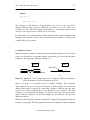
conductors. The approach is illustrated in Figure 3.1.
metal
metal
diff model
diff
locos
ground
field implant
(a)
(b)
Figure 3.1. Illustration of the heuristic approach to incorporate diffusion capacitances,
physical structure (a) and 3D capacitance model (b).
Figure 3.1.a shows a cross-sectional view of a diffused conductor. The capacitance
model employed by space3d for such a conductor is shown in Figure 3.1.b, where the
diffused interconnect is replaced by a thin sheet conductor. Therefore, the user must
specify in the element definition file a zero thickness for the conductor. The sheet
conductor is positioned half the thickness of the field oxide above the ground plane,
which is flat and continuous, and must be thought of as modeling the top side of the
diffused conductors.
Initially, the 3D capacitance extraction method will compute 3D capacitances between all
conductors and ground. The 3D capacitances between non-diffused conductors mutually,
The Nelsis IC Design System
Space 3D Capacitance Extraction
13
between non-diffused conductors and ground and between non-diffused conductors and
diffused conductors are inserted in the extracted circuit. However, the 3D capacitances
between diffused conductors and ground and between diffused conductors mutually are
better represented by junction capacitances that are computed using an area/perimeter
method.
NOTE:
Therefore, the 3D capacitances between diffused conductors and ground, and
between diffused conductors mutually, are discarded by the program. The junction
capacitances that replace these capacitances have to be specified separatedly by the
user in the element definition file.
See also Section 3.10.
Although this approach is purely heuristic, its results are satisfactory when the width of
the diffusion paths is large enough compared to the height of the sheet conductors above
the ground plane.
NOTE:
A conductor is defined as a diffused conductor within space3d if and only if in the
element definition file the type of the conductor is specified as ’n’ or ’p’.
3.9 Gate Capacitances
When extracting 3D capacitances, space3d assumes that the gate-channel capacitances of
field-effect transistor are included in the simulation model that is used for the extracted
transistor. Therefore it discards the 3D capacitance to ground for conductor parts that are
a gate of a field-effect transistor and that are directly above the transistor area as defined
in the element definition file.
Also the 3D coupling capacitances between gates and diffused conductors (drain/source
areas; see Section 3.8) can be discarded by the program, depending whether they are
present in the SPICE or other simulation model for the device. This is achieved by
turning on the parameter cap3d.omit_gate_ds_cap in the parameter file.
3.10 Non-3D Capacitances
When extracting 3D capacitances, non-3D capacitances that are specified in the element
definition file are not extracted, except for capacitances between a diffused conductor and
ground and capacitances between diffused conductors mutually (see also Section 3.8).
However, when the parameter cap3d.all_non3d_cap is set, also all non-3D capacitances
that are defined in the element definition file, are extracted.
The Nelsis IC Design System
14
Space 3D Capacitance Extraction
4. 3D Capacitance Computation
4.1 Introduction
Space3d uses a boundary-element method to compute 3D capacitances (see Appendix A).
Since there are several degrees of freedom with this method, there are also several
parameters that can be set with space3d during 3D capacitance extraction. A brief
description of these parameters is given below. For more background information on the
parameters, the reader is referred to Appendix A.
The parameters are set in the space parameter file (see also the Space User’s Manual).
All lengths and distances are specified in micron and all areas are specified in square
micron.
All parameters that have a name starting with "cap3d." may be used without this prefix if
they are included between the lines "BEGIN cap3d" and "END cap3d". E.g.
BEGIN cap3d
max_be_area
be_window
END cap3d
1
3
is equivalent to
cap3d.max_be_area
cap3d.be_window
1
3
4.2 Mesh Construction
cap3d.default_step_slope slope (default: 2.0)
Specifies the tangent of the slope of conductors (i.e. the tangent of α in the figure below)
at steps in height above the substrate (e.g. the transition of metal above polysilicon to
metal not above polysilicon). It must hold that cap3d.default_step_slope > 0.
α
NOTE:
To prevent the overlap of different transition areas of one conductor (which
currently results in incorrect element meshes), the value of parameter
cap3d.default_step_slope may not be too small.
The Nelsis IC Design System
15
Space 3D Capacitance Extraction
cap3d.max_be_area area
(no default)
This parameter specifies (in square microns) the maximum area of boundary elements
that are interior elements (i.e. elements that are not along the edges/corners of the
conductors). This parameter has no default and must therefore always be specified when
performing 3D capacitance extraction.
cap3d.min_be_area area
(default: 1 square unit)
This parameter specifies (in square microns) the minimum area of boundary elements,
which may be used (smaller areas are skipped, a warning message is given).
cap3d.edge_be_ratio float
(default: 1)
This parameter specifies the ratio between the maximum size of interior elements and the
maximum size of edge elements (edge elements are elements that are adjacent to the
edges/corners of the conductors, interior elements are the other elements, see also the
parameter cap3d.max_be_area). To efficiently compute accurate 3D capacitances it is
advantageous to use smaller elements near the edges/corners of the conductors. This is
achieved by using for cap3d.edge_be_ratio a value smaller than 1. Because the mesh
refinement is done incrementally, the size of the elements will gradually decrease towards
the edges/corners of the conductors. This is also influenced by the parameter
cap3d.edge_be_split.
cap3d.edge_be_split float
(default: 0.5)
If, during mesh refinement, a quadrilateral edge element is split into two elements (see
also the description of the parameter cap3d.edge_be_ratio), this parameter specifies the
ratio between the size of the element that becomes an edge element and the size of the
element that becomes an interior element.
cap3d.edge_be_split_lw float
(default: 4)
During mesh refinement, this parameter is used to determine the split direction of a
quadrilateral element. Interior elements are always split perpendicular to their longest
side. If the ratio between the longest side and the shortest side of an edge element does
not becomes larger than cap3d.edge_be_split_lw, an edge element is split in a direction
parallel to the edge direction. Otherwise, the edge element is split perpendicular to its
longest side. The minimum value for cap3d.edge_be_split_lw is 2.
cap3d.max_coarse_be_area float
(default: cap3d.max_be_area)
For conductors that are sheet conductors (thickness is zero) this parameter specifies (in
square microns) the maximum area of the boundary elements. When this parameter is
specified, edge elements of sheet conductors are not further refined compared interior
elements. This parameter can for example be used to model large conductor planes with
a much coarser element mesh.
The Nelsis IC Design System
16
Space 3D Capacitance Extraction
cap3d.be_shape number (default: 1)
Enforces a particular shape of the boundary element faces. Value 1 means no
enforcement. Value 3 means triangular faces (is always used in "piecewise linear" mode).
Value 4 means quadrilateral faces (is the default for constant shape functions).
4.3 Shape and Weight Functions
cap3d.be_mode mode (default: 0c)
Specifies the type of shape functions and the type of weight functions that are used (see
Section A.2).
mode
0c
0g
1g
shape function
piecewise constant
piecewise constant
piecewise linear
weight method
collocation
Galerkin
Galerkin
An example of a piecewise constant shape functions is given in Figure A.1.b. An
example of a linear shape functions is given in Figure A.1.c. Given a certain accuracy,
the Galerkin method, as compared to the collocation method, allows to use larger
elements.
cap3d.mp_min_dist distance_ratio
(default: 2.0)
When the charge- and observation-elements are not too close together, the influence
matrix element linking them can be calculated much faster (2 to 20 times) using a
multipole expansion than by numerical integration. This parameter specifies a threshold
value of the ratio between the charge-observation distance and the convergence radius of
the multipole expansion: for larger distances the multipole expansion is used, for smaller
distances numerical integration. Usually, a ratio of 1.5 is satisfactory. When setting the
parameter to infinity, all influence matrix elements are calculated by numerical
integration.
cap3d.mp_max_order 0 ... 3
(default: 2)
Specifies the highest multipole to be included in the multipole-expansion. For 0 only the
monopole is included, for 1 also the dipole, and so forth. The highest implemented value
is 3 (octopole), because on the one hand this typically suffices for a precision of one per
mil, while on the other hand the required CPU time increases drastically with the number
of multipoles.
The Nelsis IC Design System
Space 3D Capacitance Extraction
17
4.4 Accuracy of Elastance Matrix
cap3d.green_eps error
(default: 0.001)
Positive real value specifying the relative accuracy for evaluating the entries in the
elastance matrix.
cap3d.max_green_terms number (default: 500)
For dielectrics consisting of more than one layer, more than one term (iteration) will in
general be necessary to find an approximation of the Green’s function such that the error
in the entries in the elastance matrix is within cap3d.green_eps (see above). This
parameter specifies the value for the maximum number of terms that may be used. The
upper bound of this parameter is 500.
4.5 Window Size
cap3d.be_window w
cap3d.be_window wx wy
Specifies the size (in micron) of the influence window. All influences between elements
that are within a distance w will be taken into account, and all influences between
elements that are more than a distance 2w apart will not be taken into account (see
Section A.3). If only one value is given, this value specifies the size of the window in the
x direction and the y direction. If two values are given, the first value specifies the size of
the window in the x direction and the second value specifies the size of the window in the
y direction.
The extraction time is proportional to O(Nw 4 ), where N is the number of elements. The
memory usage of the program is O(w 4 ). A reasonable value for be_window is 1-3 times
the maximum height of the circuit. No default.
4.6 Discarding 3D Capacitances
cap3d.omit_gate_ds_cap boolean (default: off)
Do not extract 3D capacitances between gates and diffused conductors (drain/source
areas), see Section 3.9.
4.7 Non 3D Capacitances
cap3d.also_non3d_cap boolean (default: off)
Extract also all non-3D capacitances, see Section 3.10.
The Nelsis IC Design System
18
Space 3D Capacitance Extraction
4.8 New Cap3D Parameters
cap3d.connect_ground string
(default: @gnd)
The extraction is default using the @gnd node for ground plane connections. But you
may choice "@sub" or "distributed" instead (the @-sign may be omitted). Distributed
tries to use the substrate nodes directly below the cap3d nodes.
cap3d.spider_hash boolean (default: off)
The new space3d version does not use spider hashing to find existing spiders. Now, by
problem geometries, there can be two spiders at the same position. However, this is not
allowed for a piecewise linear be_mode (1c/1g).
cap3d.new_via_mode boolean (default: on)
Now by vias, in new mode, all calculated cap values are assigned to the top conductor via
nodes (and not more to bottom conductor nodes). This is better, because in case the
bottom conductor is a diffused conductor the cap values can be lost.
cap3d.contacts_sub boolean (default: on)
Now, the contacts to substrate are also modeled. Thus, cap values for the surfaces of
these contacts are now calculated.
cap3d.new_refine boolean (default: on)
This is an important new feature, because these mesh reductions results in a very fast
cap3d extraction. However, these refinements work only for be_mode "0c" and "0g".
cap3d.new_convex boolean (default: on)
Now, concave polygons are tried to be repaired (if possible) by shifting the spiders.
Concave polygons can be created when using e/c-shape definitions.
The Nelsis IC Design System
Space 3D Capacitance Extraction
19
4.9 Example Parameter File
An example of parameter settings for 3D capacitance extraction is as follows:
BEGIN cap3d
max_be_area
be_window
be_mode
connect_ground
contacts_sub
default_step_slope
omit_gate_ds_cap
green_eps
END cap3d
1.0
# square micron
5.0
# micron
0g
# pwc galerkin
distr
off
1.5
on
0.002
4.10 Run-time Versus Accuracy
The runtime of the program is largely dependent on the values of the parameters that are
used. For example, if max_be_area is decreased (smaller elements are used), the
accuracy will increase but also the number of elements will increase and the computation
time will become larger. The larger the size of the window, the more accurate results are
obtained but also longer extraction times will occur. The Galerkin method is more
accurate than the collocation method, but it also requires more computation time.
Also, 3D capacitance computation for configurations consisting of 2 or 3 dielectric layers
may require much more computation time than the same computation for configurations
consisting of 1 dielectric layer. This is because the computation of the Green’s functions
requires much more time. In this case, the computation time can be decreased (on the
penalty of some loss in accuracy) by increasing the value for the maximum error for the
evaluation of the entries in the elastance matrix (green_eps).
The Nelsis IC Design System
20
Space 3D Capacitance Extraction
5. Examples
5.1 Example of 5 Parallel Conductors
As a first example we show how space3d is used to compute 3D capacitances for a
configuration consisting of 5 parallel conductors. To run the example, first create a
project, e.g. with name "exam1", for an scmos_n process and lambda of 0.05 micron:
% mkpr -l 0.05 exam1
available processes:
process id
process name
1
nmos
3
scmos_n
...
select process id (1 - 60): 3
mkpr: -- project created --
Next, go to the project directory and copy the example source files from the directory
/usr/cacd/share/demo/poly5 (it is supposed that the demo directory has been installed
under /usr/cacd).
% cd exam1
% cp /usr/cacd/share/demo/poly5/* .
The layout description is put into the database using the program cgi.
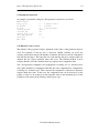
% cgi poly5.gds
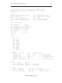
The layout of the configuration is shown below (e.g. use dali to inspect the layout). The
conductors have a length of 5 micron, a width of 0.5 micron, a height of 0.5 micron and
their separation is also 0.5 micron.
a
b
c
d
The Nelsis IC Design System
e
21
Space 3D Capacitance Extraction
An appropriate element definition file (with name "tech.s") is as follows:
% cat tech.s
unit vdimension
1e-6
# micron
colors :
cpg red
conductors :
resP : cpg : cpg : 0.0
vdimensions :
dimP : cpg : cpg : 0.5 0.5
dielectrics :
# Dielectric
# (epsilon =
SiO2
3.9
air
1.0
%
consists of 5 micron thick SiO2
3.9) on a conducting plane.
0.0
5.0
Furthermore, we use the following parameter file ("param.p"):
% cat param.p
BEGIN cap3d
be_mode
max_be_area
be_window
END cap3d
%
0c
0.5
1
Then, after having run tecc on the element definition file,
% tecc tech.s
we extract a circuit description for the layout of the cell as follows:
% space3d -C3 -E tech.t -P param.p poly5
Alternatively Xspace can be used.
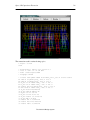
% Xspace -E tech.t -P param.p
Click button "poly5" in the menu "Database", click button "coupling cap" and "3D
capacitance" in the menu "Options", click button "DrawBEMesh", "DrawGreen" and "3
dimensional" in the menu "Display", and click button "extract" in the menu "Extract".
This will yield the following picture:
The Nelsis IC Design System
Space 3D Capacitance Extraction
22
The circuit that has been extracted can be inspected using the program xspice
% xspice -a poly5
poly5
*
*
*
*
Generated by: xspice 2.39 25-Jan-2006
Date: 20-Jun-06 10:30:48 GMT
Path: /users/space/exam1
Language: SPICE
* circuit poly5 e d c b a
c1 a b 253.3136e-18
c2 a GND 624.1936e-18
c3 b c 253.3136e-18
c4 b GND 457.9544e-18
c5 c d 253.3136e-18
c6 c GND 457.9544e-18
c7 e d 253.3136e-18
c8 e GND 624.1936e-18
c9 d GND 457.9544e-18
* end poly5
Note that there are no capacitances between conductors that are more than a distance 2 *
be_window apart (e.g. conductor "a" and conductor "d" or conductor "a" and conductor
The Nelsis IC Design System
23
Space 3D Capacitance Extraction
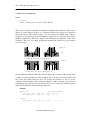
"e"). In the table below, the capacitances of conductor "a" are given as a function of the
window size. In the column denoted by C s a , the short-circuit capacitance of node "a" is
given, which is the sum of all capacitances that are connected to "a". Note that the value
of this capacitance is almost independent on the size of the window.
w
(µ) C a gnd
1 624.5
2 599.9
3 593.4
4 591.0
5 590.5
capacitances (10−18
Ca b
Ca c Ca d
253.3
256.0 16.35 7.93
256.8 16.64 7.14
257.3 17.11 7.22
257.4 17.18 7.27
F)
Ca e
4.50
4.73
4.79
The Nelsis IC Design System
Cs a
877.8
880.2
878.5
877.4
877.1
Space 3D Capacitance Extraction
24
5.2 Example of CMOS Static RAM Cell
The next example consists of a cmos static RAM cell in 0.5 µ technology. To run the
example, first create a project, e.g. with name "exam2", for an scmos_n process and
lambda of 0.25 micron:
% mkpr -l 0.25 exam2
available processes:
process id
process name
1
nmos
3
scmos_n
...
select process id (1 - 60): 3
mkpr: -- project created --
Next, go to the project directory and copy the example source files from the directory
/usr/cacd/share/demo/sram.
% cd exam2
% cp /usr/cacd/share/demo/sram/* .
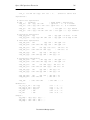
The layout of the ram cell is put into the database as follows:
% cgi sram.gds
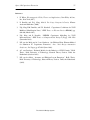
Use the layout editor dali to inspect the layout of the sram, as shown below.
The following technology file ("sram.s") is used for extraction:
The Nelsis IC Design System
25
Space 3D Capacitance Extraction
#
#
#
#
#
#
#
#
#
#
#
#
space element definition file for scmos_n example process
with vertical dimensions for conductors for 3D capacitance
extraction.
masks:
cpg - polysilicon interconnect
caa - active area
cmf - metal interconnect
cms - metal2 interconnect
cca - contact metal to diffusion
ccp
cva
cwn
csn
cog
-
contact metal to poly
contact metal to metal2
n-well
n-channel implant
contact to bondpads
See also: maskdata
unit
unit
unit
unit
unit
unit
unit
resistance
c_resistance
a_capacitance
e_capacitance
capacitance
vdimension
shape
1
1e-12
1e-6
1e-12
1e-15
1e-6
1e-6
#
#
#
#
#
#
#
ohm
ohm umˆ2
aF/umˆ2
aF/um
fF
um
um
maxkeys 10
colors :
cpg
caa
cmf
cms
cca
ccp
cva
cwn
csn
cog
cx
red
green
blue
gold
black
black
black
glass
glass
glass
glass
conductors :
# name
:
cond_mf :
cond_ms :
cond_pg :
cond_pa :
cond_na :
condition
cmf
cms
cpg
caa !cpg !csn
caa !cpg csn
:
:
:
:
:
:
mask
cmf
cms
cpg
caa
caa
fets :
# name : condition
: gate d/s
nenh : cpg caa csn : cpg caa
penh : cpg caa !csn : cpg caa
contacts :
# name
: condition
cont_s : cva cms cmf
cont_p : ccp cmf cpg
:
:
:
:
:
:
resistivity
0.045
0.030
40
70
50
:
:
:
:
:
:
type
m
m
m
p
n
#
#
#
#
#
first metal
second metal
poly interconnect
p+ active area
n+ active area
# nenh MOS
# penh MOS
: lay1 lay2 : resistivity
: cms cmf :
1
# metal to metal2
: cmf cpg : 100
# metal to poly
The Nelsis IC Design System
26
Space 3D Capacitance Extraction
cont_a : cca cmf caa !cpg : cmf
caa
: 100
# metal to active area
capacitances :
# active area capacitances
# name
: condition
: mask1 mask2 : capacitivity
acap_na : caa !cpg csn !cwn
: @gnd caa : 100 # n+ bottom
ecap_na : !caa !-cpg -csn !-cwn -caa : @gnd -caa : 300 # n+ sidewall
acap_pa : caa !cpg !csn cwn
: caa @gnd : 500 # p+ bottom
ecap_pa : !caa !-cpg !-csn cwn -cwn -caa : -caa @gnd : 600 # p+ sidewall
# polysilicon capacitances
acap_cpg_sub : cpg
!caa : cpg @gnd : 49 # bot to sub
ecap_cpg_sub : !cpg -cpg !cmf !cms !caa : -cpg @gnd : 52 # edge to sub
# first metal capacitances
acap_cmf_sub : cmf
!cpg !caa : cmf @gnd : 25
ecap_cmf_sub : !cmf -cmf !cms !cpg !caa : -cmf @gnd : 52
acap_cmf_caa : cmf
caa !cpg !cca !cca : cmf caa : 49
ecap_cmf_caa : !cmf -cmf caa !cms !cpg
: -cmf caa : 59
acap_cmf_cpg : cmf
cpg !ccp : cmf cpg : 49
ecap_cmf_cpg : !cmf -cmf cpg !cms : -cmf cpg : 59
# second metal capacitances
acap_cms_sub : cms
!cmf !cpg !caa : cms @gnd : 16
ecap_cms_sub : !cms -cms !cmf !cpg !caa : -cms @gnd : 51
acap_cms_caa : cms
caa !cmf !cpg : cms caa : 25
ecap_cms_caa : !cms -cms caa !cmf !cpg : -cms caa : 54
acap_cms_cpg : cms
cpg !cmf : cms cpg : 25
ecap_cms_cpg : !cms -cms cpg !cmf : -cms cpg : 54
acap_cms_cmf : cms
cmf !cva : cms cmf : 49
ecap_cms_cmf : !cms -cms cmf
: -cms cmf : 61
lcap_cms
: !cms -cms =cms
vdimensions :
ver_caa_on_all
ver_cpg_of_caa
ver_cpg_on_caa
ver_cmf
ver_cms
:
:
:
:
:
caa !cpg
cpg !caa
cpg caa
cmf
cms
: -cms =cms : 0.07
:
:
:
:
:
caa
cpg
cpg
cmf
cms
:
:
:
:
:
eshapes :
cpg_edge : !cpg -cpg : cpg : 0 0
cmf_edge : !cmf -cmf : cmf : 0 0
cms_edge : !cms -cms : cms : 0 0
The Nelsis IC Design System
0.30
0.60
0.35
1.70
2.80
0.00
0.50
0.70
0.70
0.70
27
Space 3D Capacitance Extraction
dielectrics :
# Dielectric
# (epsilon =
SiO2
3.9
air
1.0
consists of 5 micron thick SiO2
3.9) on a conducting plane.
0.0
5.0
#EOF
Note that for the diffusion area a conductor of thickness 0 is used that is 0.30 µ above the
substrate.
The contents of the parameter file ("sram.p") is as follows:
BEGIN cap3d
be_mode
be_window
max_be_area
omit_gate_ds_cap
END cap3d
0c
2.0
1.0
on
After running tecc on the element definition file,
% tecc sram.s
extraction in batch mode is done by using space3d.
% space3d -C3 -E sram.t -P sram.p sram
For interactive extraction, Xspace is used.
% Xspace -E sram.t -P sram.p
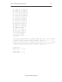
Click button "sram" in the menu "Database", click button "coupling cap" and "3D
capacitance" in the menu "Options", click button "DrawBEMesh", "DrawGreen" and "3
dimensional" in the menu "Display", and click button "extract" in the menu "Extract".
This will yield the following picture:
The Nelsis IC Design System
Space 3D Capacitance Extraction
The extraction result is retrieved using xspice:
% xspice -a sram
sram
*
*
*
*
Generated by: xspice 2.39 25-Jan-2006
Date: 20-Jun-06 10:40:34 GMT
Path: /users/space/exam2
Language: SPICE
* circuit sram pbulk nbulk word vdd b_vss t_vss c1 c2 bit notbit
m1 vdd c1 c2 pbulk penh_0 w=500n l=500n
m2 vdd c2 c1 pbulk penh_0 w=500n l=500n
m3 b_vss c1 c2 nbulk nenh_0 w=500n l=500n
m4 t_vss c2 c1 nbulk nenh_0 w=500n l=500n
m5 notbit word c2 nbulk nenh_0 w=500n l=500n
m6 bit word c1 nbulk nenh_0 w=500n l=500n
c1 b_vss word 114.8418e-18
c2 b_vss vdd 43.84559e-18
c3 b_vss c2 74.079e-18
c4 b_vss c1 212.2091e-18
c5 b_vss notbit 610.2115e-18
c6 b_vss GND 1.80899f
c7 notbit bit 107.3522e-18
c8 notbit word 115.7189e-18
c9 notbit vdd 6.609528e-18
The Nelsis IC Design System
28
Space 3D Capacitance Extraction
29
c10 notbit c2 360.549e-18
c11 notbit c1 66.39728e-18
c12 notbit GND 2.597814f
c13 t_vss word 114.8457e-18
c14 t_vss vdd 43.82952e-18
c15 t_vss bit 610.3344e-18
c16 t_vss c2 212.2316e-18
c17 t_vss c1 73.78773e-18
c18 t_vss GND 1.808788f
c19 word bit 115.8338e-18
c20 word c2 113.7943e-18
c21 word c1 111.6566e-18
c22 word GND 344.449e-18
c23 vdd bit 6.60235e-18
c24 vdd c2 56.77325e-18
c25 vdd c1 58.65703e-18
c26 vdd GND 9.5875f
c27 bit c1 360.2213e-18
c28 bit c2 67.05254e-18
c29 bit GND 2.597536f
c30 c2 c1 998.1198e-18
c31 c2 GND 5.426256f
c32 c1 GND 5.425883f
* end sram
.model penh_0 pmos(level=2 ld=0 tox=25n nsub=50e15 vto=-1.1 uo=200 uexp=100m
+ ucrit=10k delta=200m xj=500n vmax=50k neff=1 rsh=0 nfs=0 js=10u cj=500u
+ cjsw=600p mj=500m mjsw=300m pb=800m cgdo=300p cgso=300p)
.model nenh_0 nmos(level=2 ld=0 tox=25n nsub=20e15 vto=700m uo=600 uexp=100m
+ ucrit=10k delta=200m xj=500n vmax=50k neff=1 rsh=0 nfs=0 js=2u cj=100u
+ cjsw=300p mj=500m mjsw=300m pb=800m cgdo=300p cgso=300p)
vpbulk pbulk 0 5
rpbulk pbulk 0 100meg
vnbulk nbulk 0 0
rnbulk nbulk 0 100meg
The Nelsis IC Design System
Space 3D Capacitance Extraction
30
6. Solving Problems
6.1 Long Computation Times
Although space3d has been implemented with emphasis on efficient 3D capacitance
extraction methods, sometimes long extraction times may occur. This for example
happens if too much time is spend on the computation of irrelevant details. This is for
example the case if the size of the elements is chosen too small, if the window size is
unnecessary large or if linear shape functions and the Galerkin method are used for too
many elements. A good strategy to circumvent this problem is to first try an extraction
with a parameter set that does not include many details. Next, a parameter set is used in
which more details are included, and the extraction results are evaluated to inspect the
influence of the parameters. See also Section 4.10.
6.2 Numerical Problems
If the elastance matrix (see Section A.2) is badly conditioned, space3d may be unable to
invert this matrix and it may give error messages like "domain error(s) in sqrt". One
reason for a badly conditioned elastance matrix is that there is too much difference in
element sizes. A solution in this case is to split the large elements, either by decreasing
the maximum size of the elements or by adding irregularities to the layout using a
symbolic mask. If very thin conductors are used, the difference between the small
vertical elements and the large horizontal elements may also become too large. In this
case, it may for example be better to specify a zero thickness for the conductor in the
element definition file. In general, the creation of small elements that are close to large
elements, and the creation of long and narrow elements, should be avoided.
Also the use of the Galerkin method (be_mode 0g or 1g) instead of the collocation
method (be_mode 0c) might help in the above case.
6.3 Negative Capacitances
Some element meshes may also give rise to negative capacitances. Negative capacitances
may for example occur when conductors are close to each other and relatively large
elements are used. A typical example is the situation where the bottom of a transistor
gate approaches its adjacent drain/source regions. More accurate results (without
negative capacitances) are then obtained by (1) decreasing the maximum size of the
elements and/or (2) increasing the height of the bottom of the gate above the substrate. If
necessary, the parameters min_coup_cap and/or no_neg_cap can be set to remove the
remaining (small) negative capacitances.
The Nelsis IC Design System
Space 3D Capacitance Extraction
31
6.4 Mesh Generation Problems
If space3d gives error messages like "mesh.c, 846: assertion failed" or "refine.c, 507:
assertion failed", there is something wrong with mesh generation. This problem is often
caused by the modeling of the steps in height above the substrate of the conductors. If
the slope of a conductor near such a transition area is too small, different transition areas
may overlap and the program will not be able to generate a correct mesh (see Section 3.3
and Section 4.2).
Mesh generation problems may also be caused by the use of eshapes (see Section 3.4)
and by the fact that, because of the use of a window (parameter cap3d.be_window), long
and narrow mesh elements may be generated. Sometimes, problems due to the first cause
are solved by using a resize statement in the element definition file (see Space User’s
Manual) instead of an eshape statement.
The Nelsis IC Design System
32
Space 3D Capacitance Extraction
Appendix A: 3D Capacitance Model
A.1 Introduction
Space3d uses a boundary-element method to compute 3D capacitances. A brief
description of this method is given in Section A.2. For the solution of the boundaryelement equations, a large matrix needs to be inverted. The approximate matrix inversion
technique that is used for this is described in Section A.3.
A.2 The Boundary-Element Method
Consider a domain V that contains M conductors. Our purpose is to find the short-circuit
capacitance matrix C s that gives the relation between the conductor charges
QT = [Q1 , Q2 , . . . Q M ] and the conductor potentials ΦT = [Φ1 , Φ2 , . . . Φ M ] as
Q = C s Φ.
(A.1)
The potential φ ( p) at a point p in V can be expressed as [1, 2]
φ ( p) =
∫V G( p, q) ρ (q) dq,
(A.2)
where ρ (q) is the charge distribution in V and G( p, q) is the Green’s function for V . In
order to solve A.2, the boundary-element method subdivides the surfaces of the
conductors in elements S 1 , S 2 , . . . S N (the elements may partly be overlapping), and
approximates the charge distribution ρ (q) by
ρ (q) ≈ ρ̃ (q) =
N
Σ αi
f i (q),
(A.3)
i=1
where α 1 , α 2 , . . . α N are unknown variables to be determined and f 1, f 2 , . . . f N are N
independent shape functions (also called basis functions). The f i ’s have the property that
∫
S
j
1
f i (q) dq =
0
if i = j
if i ≠ j
(A.4)
Some examples of shape functions are given in Figure A.1.
An approximation for the potential distribution is then obtained by insertion of A.3 into
A.2:
φ˜( p) =
N
Σ α i ∫ G( p, q)
i=1
f j (q) dq.
(A.5)
Si
Next, N independent linear equations are obtained by introducing a set of N independent
weight functions w 1 , w 2 , . . . w N that are defined on the sub-areas S 1 , S 2 , . . . S N and that
The Nelsis IC Design System
33
Space 3D Capacitance Extraction
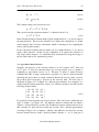
f i ( p)
f i ( p)
f i ( p)
Si
Si
(b)
(c)
Si
(a)
Figure A.1. Different types of shape or basis functions that can be used to model the
surface charge density on the conductors (a) Dirac, (b) constant: f is
described by the top of the wedge, (c) linear: f is described by the 4 slanting
planes of the pyramid.
are used to "average out" the error in φ˜( p):
∫S wi ( p) φ˜( p) − φ ( p)dp
= 0
(i = 1 . . . N ).
(A.6)
i
By insertion of A.5, the above set of equation may be rewritten as
N
Σ α j ∫ ∫ G( p, q)
j=1
f j (q) w i ( p) dq dp =
Si S j
∫S wi ( p) φ ( p)
i
dp
(i = 1 . . . N ). (A.7)
Now, let F be an N × M incidence matrix in which
1
F ij =
0
if S i is on conductor j
otherwise.
(A.8)
Then, Equation A.7 may be written as a set of N × N equations,
G α = W F Φ,
(A.9)
where G is an N × N matrix that has entries
G ij =
∫ ∫ G( p, q) f j (q) wi ( p) dq dp,
Si S j
α T = [α 1 , α 2 , . . . , α N ], and W is an N × N matrix that has entries
The Nelsis IC Design System
(A.10)
Space 3D Capacitance Extraction
W ij = 0,
W ii =
i ≠ j,
34
(A.11a)
∫S wi ( p) dp.
(A.11b)
i
The conductor charges are found from A.9 as
Q = F T α = F T G −1 W F Φ.
(A.12)
Thus, the short-circuit capacitance matrix C s is obtained from A.12 as
C s = F T G −1 W F.
(A.13)
In the Galerkin boundary-element method [3] the weight functions w i are chosen equal to
the shape functions. This way, the evaluation of G requires the computation of a double
surface integral, but G becomes symmetrical, which is advantageous for computing the
inverse of the elastance matrix.
In the collocation boundary-element method [4], the weight functions w i are chosen
equal to Dirac functions. In this case the computation of G requires the evaluation of
only single surface integrals. G is artificially made symmetrical by using the average of
the two entries that are at a symmetrical position.
A.3 Approximate Matrix Inversion
Normally, the inversion of the elastance matrix G in A.13 requires O(N 3 ) time and
O(N 2 ) space. To allow fast extraction times, also for large circuits, space is capable of
computing an approximate inverse for G. Therefore, it utilizes a matrix inversion
technique that takes as input a matrix that is specified on a stair-case band around the
main diagonal and produces as output a matrix in which only non-zero entries occur for
the positions that correspond to positions in the stair-case band. The basic idea is
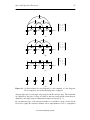
illustrated in Figure A.2. In Figure A.2, different approximations are computed for a
simple boundary-element mesh that consists of 4 elements and that is described by the
following elastance matrix:
1. 0
0. 4
0. 2
0. 1
0. 4
1. 0
0. 4
0. 2
0. 2
0. 4
1. 0
0. 4
0. 1
0. 2
0. 4
1. 0
(A.14)
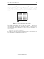
For practical layouts the method proceeds as follows. First, the layout is subdivided into
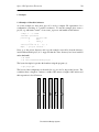
strips of width w (see Figure A.3). All influences between elements that are within a
distance w will be taken into account, and all influences between elements that are more
than a distance 2w apart will not be taken into account. Next, a banded approximation
according to Figure A.2 is computed - whereby only influences are taken into account
between elements that are in the y direction within a distance w - for (1) each pair of
The Nelsis IC Design System
35
Space 3D Capacitance Extraction
0.007
0.054
•
•
1
0.454
0.678
0.054
•
2
0.434
0.424
•
3
0.454
0.424
x
x
x
x
4
x
x
x
x
x
x
x
x
x
x
x
x
0.678
(a)
0.059
•
•
0.455
0.681
0.059
•
0.433
0.421
x x x
x x x x
x x x x
x x x
•
0.455
0.421
0.681
(b)
•
•
0.476
0.714
•
0.476
0.429
x x
x x x
x x x
x x
•
0.476
0.429
0.714
(c)
x
•
•
•
x
•
x
x
1
1
1
1
(d)
Figure A.2. (a) Exact solution, (b) only diagonals 1-3 are computed, (c) only diagonals
1-2 are computed, (d) only the main diagonal is computed.
adjacent strips and (2) each single strip except for the first and last strip. The results that
are obtained for the pairs of strips are added to the total result and the results that are
obtained for the single strips are subtracted from the total result [5, 6, 7].
By executing all steps of the extraction method as a scanline is swept over the layout
from left to right, the extraction method can be implemented to have a computation
The Nelsis IC Design System
Space 3D Capacitance Extraction
36
complexity that is O(Nw 4 ) and a memory usage that is O(w 4 ). So, when w is kept
constant, which is reasonable if one type of technology is used, the computation
complexity of the method is linear with the size of the circuit and the space complexity is
constant.
w
Figure A.3. A layout subdivided into strips of width w.
Note that the calculated Green values of a single strip are written to temporary files
(space1.xxxxxx and space2.xxxxxx). The program is using one of the directories of
environment variable SPACE_TMPDIR. If you want to check these Green buffers you
can use parameter:
debug.check_green boolean (default: off)
If "on" the Green values are recalculated and checked against the values read from the
Green buffer. Thus you can check the Green buffers used.
The Nelsis IC Design System
Space 3D Capacitance Extraction
37
References
1.
E. Weber, Electromagnetic Fields, Theory and Applications, John Wiley & Sons,
Inc., New York (1957).
2.
P. Dewilde and Z.Q. Ning, Models For Large Integrated Circuits, Kluwer
Academic Publishers (1990).
3.
Z.Q. Ning, P.M. Dewilde, and F.L. Neerhoff, ‘‘Capacitance Coefficients for VLSI
Multilevel Metallization Lines,’’ IEEE Trans. on Electron Devices ED-34(3) pp.
644-649 (March 1987).
4.
Z.Q. Ning and P. Dewilde, ‘‘SPIDER: Capacitance Modelling for VLSI
Interconnections,’’ IEEE Trans. on Computer-Aided Design 7(12) pp. 1221-1228
(December 1988).
5.
N.P. van der Meijs and A.J. van Genderen, ‘‘An Efficient Finite Element Method
for Submicron IC Capacitance Extraction,’’ Proc. 26th Design Automation
Conference, Las Vegas, pp. 678-681 (June 1989).
6.
A.J. van Genderen, ‘‘Reduced Models for the Behavior of VLSI Circuits,’’ Ph.D.
Thesis, Delft University of Technology, Network Theory Section, Delft, the
Netherlands (October 1991).
7.
N.P. van der Meijs, ‘‘Accurate and Efficient Layout Extraction,’’ Ph.D. Thesis,
Delft University of Technology, Network Theory Section, Delft, the Netherlands
(1992).
The Nelsis IC Design System
CONTENTS
1. Introduction...............................................................................................................
1.1 3D Capacitance Extraction ..............................................................................
1.2 Space Characteristics .......................................................................................
1.3 Documentation.................................................................................................
1.4 On-line Examples.............................................................................................
1
1
1
1
2
2. Program Usage ..........................................................................................................
2.1 General.............................................................................................................
2.2 Batch Mode Extraction ....................................................................................
2.3 Interactive Extraction .......................................................................................
3
3
3
3
3. Technology Description ............................................................................................
4
3.1 Introduction......................................................................................................
4
3.2 Unit Specification.............................................................................................
4
3.3 The Vertical Dimension List ............................................................................
4
3.4 The Edge Shape List ........................................................................................
6
3.5 The Cross-over Shape List...............................................................................
7
3.6 Dielectric Structure ..........................................................................................
8
3.7 Additional Parameters in the Dielectrics Section ............................................
8
3.8 Diffused Conductors ........................................................................................ 12
3.9 Gate Capacitances ............................................................................................ 13
3.10 Non-3D Capacitances ...................................................................................... 13
4. 3D Capacitance Computation ...................................................................................
4.1 Introduction......................................................................................................
4.2 Mesh Construction ...........................................................................................
4.3 Shape and Weight Functions............................................................................
4.4 Accuracy of Elastance Matrix..........................................................................
4.5 Window Size ....................................................................................................
4.6 Discarding 3D Capacitances ............................................................................
4.7 Non 3D Capacitances.......................................................................................
4.8 New Cap3D Parameters ...................................................................................
4.9 Example Parameter File ...................................................................................
4.10 Run-time Versus Accuracy ..............................................................................
14
14
14
16
17
17
17
17
18
19
19
5. Examples................................................................................................................... 20
5.1 Example of 5 Parallel Conductors ................................................................... 20
5.2 Example of CMOS Static RAM Cell............................................................... 24
6. Solving Problems ...................................................................................................... 30
6.1 Long Computation Times ................................................................................ 30
6.2 Numerical Problems......................................................................................... 30
6.3 Negative Capacitances ..................................................................................... 30
6.4 Mesh Generation Problems.............................................................................. 31
-i-
Appendix A: 3D Capacitance Model............................................................................. 32
A.1 Introduction...................................................................................................... 32
A.2 The Boundary-Element Method ...................................................................... 32
A.3 Approximate Matrix Inversion......................................................................... 34
References ...................................................................................................................... 37
- ii -
LIST OF FIGURES
Figure 3.1. Illustration of the heuristic approach to incorporate diffusion
capacitances, physical structure (a) and 3D capacitance model
(b)...............................................................................................................
12
Figure A.1. Different types of shape or basis functions that can be used to model
the surface charge density on the conductors (a) Dirac, (b) constant: f
is described by the top of the wedge, (c) linear: f is described by the 4
slanting planes of the pyramid. ..................................................................
33
Figure A.2. (a) Exact solution, (b) only diagonals 1-3 are computed, (c) only
diagonals 1-2 are computed, (d) only the main diagonal is
computed. ..................................................................................................
35
Figure A.3. A layout subdivided into strips of width w................................................
36
- iii -