1
SLS : SWITCH-LEVEL SIMULATOR
USER’S MANUAL
A. C. de Graaf
A. J. van Genderen
Department of Electrical Engineering
Delft University of Technology
The Netherlands
Copyright 1987 by the authors.
All rights reserved.
Date:
Last revision:
October, 1987.
October, 1994.
Sls User’s Manual
1
1. INTRODUCTION
This manual is meant as a guide to users who want to simulate their network with the sls
simulator. The acronym sls stands for Switch-Level Simulator, and the simulator can be
used for simulating the logical and timing behavior of digital MOS circuits. In the
simulator transistors are modeled by grounded capacitors and a switched resistor. Each
node in the network has a logic state O, I or X (for unknown), and each transistor has a
state on, off or undefined. Many characteristics of MOS circuits can be modeled
accurately, including: ratioed, complementary and precharged logic; dynamic and static
storage; pass transistors; busses; and charge sharing. Because the simulator performs
local-event-driven simulation, large networks with thousands of transistors can be
simulated in a reasonable time.
The sls simulator is capable of simulating a MOS transistor network at three levels:
1.
purely logic simulation based on network topology and transistor types, without
considering the actual circuit parameters.
2.
logic simulation based on actual circuit parameters (transistor dimensions and
interconnection resistances and capacitances are used to determine logic states).
3.
logic and timing simulation based on actual circuit parameters (transistor
dimensions and interconnection resistances and capacitances are used to determine
logic states and delays).
Other important features of the simulator are:
g
piece-wise-linear voltage waveform approximations with timing simulation.
g
min-max delay simulation to account for circuit parameter deviations and model
accuracy.
g
mixed-level simulation for transistor-level, gate-level and function-level circuits.
The original switch-level model - which only allows a simulation at the first level - was
introduced by R.E. Bryant. Descriptions of it are given in [1] and [2]. In [3, 4] and [5]
the principle of the sls simulator is described. The limitations of the simulator can also
be found there: Due to its simple transistor model, sls is not as accurate as a circuit
simulator like SPICE [6], while sometimes the transistor-level description of analogue
circuits like sense amplifiers can not be simulated correctly at all.
Section 2 in this manual gives an overview of the sls package of programs.
Section 3 describes the syntax and semantics of the network description language.
Section 4 contains the syntax and semantics of the command language.
Section 5 gives some suggestions for solving troubles.
The use of function-level circuit descriptions in the sls simulator is explained in [7].
The Nelsis IC Design System
Sls User’s Manual
2
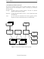
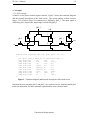
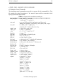
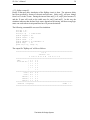
2. DESCRIPTION OF THE SLS-PACKAGE
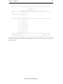
The switch level simulation package consists of a number of programs. In Figure 1 the
relation between the three main programs is outlined. In this figure you will find the
following symbols:
Rectangle
Rectangles stand for executable programs. The name of a particular
program is printed inside the rectangle.
Punch-card
A punch-card symbol stands for one file. A deck of punch-cards stands
for multiple files.
Arrow
An arrow denotes the information flow between programs and files.
Programs can read/write information from/to several different files.
network
file
command
file
sls_mkdb
sls_exp
sls
cell.out
file
cell.res
file
network
db-format
binary file
for sls
database
Figure 1. Information flow diagram of the SLS-package.
The Nelsis IC Design System
cell.plt
file
Sls User’s Manual
3
The SLS-package involves three main programs.
1.
sls_mkdb maps a hierarchical sls network description contained in one or several
files into a network description in database format.
2.
sls_exp maps the network description in database format into a binary (i.e. non
readable) file which serves as input file for the switch level simulator. Actually a
collection of binary files can be created in the database, because first a binary file
for each subnetwork is created once. The expansion program links the binary files
of the subnetworks into one binary file of the total network. Normally, sls_exp is
automatically called by sls when starting a simulation.
3.
sls is the switch level simulation program and reads input from two files:
A binary file
This file is generated by sls_exp and contains the network
description in binary format.
A command file
This file contains the simulation commands and must be
generated manually by the designer.
the output files that can be generated by sls are:
cell.out
This file is the normal readable and printable output in table format.
Here "cell" stands for the name of the cell that is simulated.
cell.res
This file is not readable and serves as input for several post
processing facilities or as input for new simulations.
cell.plt
This file is only generated when approximating voltage waveforms
are plotted. The file is not readable but can be used as input for a
post-processor.
cell.dis
This file is optionally generated when information about the dynamic
dissipation in the circuit is requested.
Other programs that belong to the SLS-package involve post processing facilities
producing different sorts of output. E.g. lpsig can be used to plot simulation output on a
printer, and simeye is a graphical signal display and editing program.
For the invocation of the programs above, see the manual pages in the appendix of this
manual.
Apart from using the program sls_mkdb to put a network description into the database,
also other programs may be used to generate an input network for sls, like the layout to
circuit extraction program space.
The Nelsis IC Design System
Sls User’s Manual
4
3. THE DESCRIPTION OF NETWORKS
3.1 General conventions.
It is common practice to describe the syntax of a computer language in some meta
language. The syntax definition of sls is described in the meta language proposed by
Wirth [8]. This language has two types of symbols:
terminal symbols
These symbols are denoted by characters between double
quote marks, or words printed in italic font. They must be
used literally or are described in the table "lexical
constructions".
non-terminal symbols
These are denoted by words in the ordinary font, and each of
them is described by a so-called production rule.
Each production rule of the sls syntax begins with a non-terminal, followed by an equalsign and a sequence of terminal and non-terminal symbols and meta characters, and is
terminated by a period. The meta characters imply:
Alternatives |
A vertical bar between symbols denotes the choice of either one
symbol or another symbol. (i.e. a | b means either a or b)
Repetition {}
Curly brackets denote that the symbols in between may be present
zero or more times.
(i.e. { a } stands for empty | a | aa | aaa | ...)
Optionality []
Square brackets denote that the symbols between them may be
present.
(i.e. [ a ] stands for a | empty)
Parenthesis ()
Parenthesis serve for grouping of symbols in meta character
expressions.
(i.e. ( a | b ) c stands for ac | bc)
Next the following rules are applied:
— A comment begins with "/*" and is terminated by "*/" as in the C-language. Every
character in between is discarded by the parser. You are not allowed to nest
comments.
— A name or identifier must begin with a letter and may be followed by an arbitrary
number of letters, digits and underscore characters.
— Uppercase and lowercase letters are distinct.
— The blank, tab and newline are separators. Between two symbols of a production rule
of a non-terminal symbol, an arbitrary number of separators may appear.
The Nelsis IC Design System
Sls User’s Manual
5
— Values are specified in S.I. units (e.g. meter, farad, ohm), and may appear with one of
the following scaling factors:
f
p
n
u
m
k
M
G
= 1.0e-15
= 1.0e-12
= 1.0e-9
= 1.0e-6
= 1.0e-3
= 1.0e+3
= 1.0e+6
= 1.0e+9
— Terminal symbols that are not literal are described in the next table. The difference
between this syntax description (of terminal symbols) and following syntax
descriptions (of non-terminal symbols) is that here it is not allowed to use separators
between the symbols that make up the production rule.
TABLE 1. Lexical constructions
iiiiiiiiiiiiiiiiiiiiiiiiiiiiiiiiiiiiiiiiiiiiiiiii
power_ten
f_float
float
exponent
identifier
string
character
integer
letter
digit
empty
special
= "1"{"0"}[("f"|"p"|"n"|"u"|"m"|"k"|"M"|"G")].
= float[("f"|"p"|"n"|"u"|"m"|"k"|"M"|"G")].
= integer["."integer][exponent]
= ("D"|"E"|"d"|"e")[("-"|"+")]integer.
= letter {(letter | digit | "_")}.
= """ character { character } """.
= digit | letter | special.
= digit {digit}.
= "a"|"b"|"c"|"d"|"e"|"f"|"g"|"h"|"i"|"j"
| "k"|"l"|"m"|"n"|"o"|"p"|"q"|"r"|"s"|"t"
| "u"|"v"|"w"|"x"|"y"|"z"
| "A"|"B"|"C"|"D"|"E"|"F"|"G"|"H"|"I"|"J"
| "K"|"L"|"M"|"N"|"O"|"P"|"Q"|"R"|"S"|"T"
| "U"|"V"|"W"|"X"|"Y"|"Z".
= "0"|"1"|"2"|"3"|"4"|"5"|"6"|"7"|"8"|"9".
= "".
= any character that is not a letter, digit or """.
Examples:
power_ten : 10n 100p 1000u
f_float : 1.3e-9 2.0n 6.8k 0.0004
identifier : abcd a123 this_IS_an_identifier
string : "this is a string/$*&"
The Nelsis IC Design System
Sls User’s Manual
6
3.2 Network Description
TABLE 2. Syntax of the network part.
iiiiiiiiiiiiiiiiiiiiiiiiiiiiiiiiiiiiiiiiiiiiiiii
network_decls
network_decl
= network_decl {network_decl}.
= network identifier decl_part ntw_body.
The network part begins with the keyword network followed by the name of the network,
a declaration part describing the interface to the outside world and a body specifying the
instances of devices and subnetworks.
3.3 Declarations
TABLE 3. Syntax of the declaration part.
iiiiiiiiiiiiiiiiiiiiiiiiiiiiiiiiiiiii
decl_part
term_decls
term decl
term
range_list
range
= "(" term_decls ")".
= term_decl {";" term_decl}.
= terminal term {"," term}.
= identifier ["[" range_list "]"].
= range {"," range}.
= integer ".." integer.
The declaration part is bracketed by a left and right parenthesis. It must contain at least
one terminal declaration. A terminal declaration begins with the keyword terminal
followed by a list of terminals. A list of terminals consists of one or more terminals
separated by commas.
Examples:
network register (terminal in[1..4,1..4], out[1..8])
network latch (terminal in, out;
terminal phi[0..1], vss, vdd)
3.4 Network Structure
The network body (ntw_body) is the statement part (stmt_part) bracketed by curly
brackets ({}). The statement part may contain instance, net and null statements. The
scope of the terminal, instance and node names in the network is local to the defined
network.
The Nelsis IC Design System
Sls User’s Manual
7
TABLE 4. Syntax of the network body.
i
iiiiiiiiiiiiiiiiiiiiiiiiiiiiiiiiiiiiiiiiiiiiiiiii
ntw_body
stmt_part
statement
inst_stmt
inst_struct
inst_def
null_stmt
net_stmt
net_spec
vector_list
net_nodes
transistor_def
ttype
function_def
ftype
resistor_def
capacitor_def
call_def
attributes
attribute
attr_label
attr_val
connect_list
connects
connect
internal_ref
node_ref
index_list
index
range_list
range
= "{" stmt_part "}".
= statement {statement}.
= inst_stmt | net_stmt | null_stmt.
= [inst_struct] inst_def.
= "{" identifier [ "[" range_list "]" ] }"
| "{" "." "[" range_list "]" }".
= transistor_def | function_def | resistor_def
| capacitor_def | call_def.
= ";".
= net "{" net_spec "}" ";".
= vector_list | net_nodes ";".
= "(" net_nodes ")" {"," "(" net_nodes ")"}.
= node_ref {"," node_ref}.
= ttype [attributes] connect_list ";".
= nenh | penh | ndep.
= "@" ftype [attributes] connect_list ";".
= invert | nand | nor | and | or | exor.
= res f_float connect_list ";".
= cap f_float connect_list ";".
= identifier connect_list";".
= attribute {attribute}.
= attr_label "=" attr_val.
= w | l | tr | tf.
= f_float.
= "(" connects ")" | "{" connects "}".
= connect {"," connect}.
= internal_ref | node_ref.
= [ "[" index_list "]" ] "." node_ref.
= integer | identifier [ "[" index_list "]" ].
= index {"," index}.
= integer | range.
= range {"," range }.
= integer ".." integer.
3.4.1 instance statement.
The instance statement constitutes the actual place of a device, function or subnetwork in
the network being defined. An instance may optionally have a structure part and must
have a definition part. The instance name in the structure part is especially convenient
for selecting particular nodes within the instance (as might be necessary in the simulation
command file). The instance may have an array structure, which is specified by a range
The Nelsis IC Design System
Sls User’s Manual
8
list between square brackets after the instance name. The general format of an instance
definition is:
type
attributes
connect_list
In each definition a node connection list is specified. This list can be interpreted in two
ways:
instance major order
If the list is placed between parenthesis we define it to be in
instance major order. Instance major order means that when
the instance has array structure, for instance from 1 to 4, the
connection list will be interpreted as follows, first all the
terminal connections for the first array element, then that of
the second array element, etc..
parameter major order
If the list is placed between curly brackets we define it to be
in parameter major order. Parameter major order means that
if the instance has array structure, the connection list will
consist of first the first terminals of all array elements, then
the second terminals of all array elements etc..
Examples:
{ inv[1..3] } inverter ( i1, o1,
i2, o2,
i3, o3 );
{ inv[1..3] } inverter { i1, i2, i3,
o1, o2, o3 };
{ inv[1..3,1..3] } inverter { in[1..9], out[1..9] };
When "inverter" has terminals i and o, in the first two examples i1 will be connected
inv[1].i, o1 to inv[1].o, i2 to inv[2].i, o2 to inv[2].o, i3 to inv[3].i and o3 to inv[3].o.
the third example, in[1] will be connected to inv[1,1].i, in[2] to inv[1,2].i, in[3]
inv[1,3].i, in[4] to inv[2,1].i, etc. out[1] to inv[1,1].o, out[2] to inv[1,2].o, out[3]
inv[1,3].o, out[4] to inv[2,1].o, etc.
to
In
to
to
If the instance is an array of elements one can specify internal connections in the
connection list. With an internal connection one can directly interconnect terminals of
the array elements of the instance. An internal connection is denoted by selecting a
formal terminal of an instanced (possibly array) element and is put into the right place in
the connection list.
The Nelsis IC Design System
Sls User’s Manual
9
Example:
{ inv[1..3] } inverter { i1, [1..2].o, [2..3].i, o3 };
where inverter was defined as
network inverter (terminal i, o)
{
.
.
.
}
The next subsections describe the instance definition parts that can occur.
3.4.1.1 transistor definition.
A transistor definition contains three arguments.
type
specifies the type of the transistor. The following three types can be
chosen:
1.
2.
3.
nenh
penh
ndep
attributes
The second argument is optional and specifies the attribute values of the
device. A transistor can have two attributes for specifying the length and
width of a transistor. If omitted the default values for length and width of
the transistor are 4 micron for sls.
connection
The third argument consists of three or a multiple of three node
references, depending on the structure of the instance. The sequence of
the nodes is important as far as the gate node is concerned. The gate node
must be specified as the first node, while the sequence of the source node
and drain node is arbitrary.
Examples:
nenh w=6u l=8u (g1, d1, s1);
{ n1 } penh w=6u l=8u (g1, d1, s1);
{ ni[1..2] } nenh (g1, d1, s1, g2, d2, s2);
{ np[1..2] } ndep {g1, g2, d1, d2, s1, s2};
The Nelsis IC Design System
Sls User’s Manual
10
3.4.1.2 function definition.
A function definition calls a network element that reads its inputs and produces logical
states at its output(s). Gate-level functions like nands and nors are available as built-in
functions while other, more complex functions (e.g. adders, multiplexers and roms) can
be specified by the user (see [7]).
A function definition contains four arguments:
specifier
A function specifier which consists of the character "@".
type
The type of the function element. The following function types are
available as built-in functions:
1.
2.
3.
4.
5.
6.
invert
nand
nor
and
or
exor
attributes
The attributes tr and tf are optional and specify the rise time and fall time
of the output(s) when the logic state of one of the inputs changes. Default
tr=0 and tf=0.
connection
Specifies the connection of the function inputs and outputs to the network
nodes. The connection list of a built-in function may contain an arbitrary
number of input nodes (except for function "invert" which may contain
only one input node) and one output node. The order is first the input
nodes and then the output node.
When two or more function outputs are connected to the same network node and not all
outputs force the same state, the X state will result.
Examples:
@ nand (a, b, c, d, e, out);
{ nands[1..2] } @ nand (a, b, out1, c, d, out2);
@ nor tr=10n tf=5n (a, b, c, d, out);
3.4.1.3 resistor definition.
The resistor definition is specified by the keyword res, the resistance value in Ohm and
two node references. The resistance value may be a floating point number and may have
a multiplication factor denoted by a letter as described in section 1.
The Nelsis IC Design System
Sls User’s Manual
11
Example:
res 2k (a, out);
3.4.1.4 capacitor definition.
The capacitor definition is specified by the keyword cap, a capacitance value in Farad
and two node references. The capacitance value may be a floating point number with a
multiplication factor.
Example:
cap 8.6f (12, a);
3.4.1.5 call definition.
A network call defines the instance of a subnetwork. The sequence of the connection list
is the same as the sequence of the terminal declaration of the called network.
Example:
when network subntw was defined as
network subntw (terminal in[1..2], out, vdd, vss)
{
.
.
}
the instance
subntw (a, b, c, vdd, vss);
will connect a to in[1], b to in[2], c to out, vdd to vdd, and vss to vss.
3.4.2 net statement.
The net statement gives the opportunity to coalesce, cluster and define nodes. This
statement is especially convenient if the network description is extracted from a layout
description. In a layout description terminals often represent the same electrical node
and it would be tedious to specify a stimulus for each of these terminals.
coalesce
Normally all specified terminals between curly brackets are coalesced to
one electrical node.
The Nelsis IC Design System
Sls User’s Manual
12
cluster
A list of parenthesized lists of terminals means that the the terminals
between the parenthesis will be coalesced element wise. The number of
elements in all parenthesized lists must be equal!
define
If a terminal in the list between curly brackets is not defined it will be
defined and can function as local node.
Examples:
net { a[1..8], b, c }; /* connect to one */
net { (a[1..4]), (b, c, d, e) }; /* connect element wise */
net { (a[1..4]) }; /* define local array */
3.5 External Network Declaration
TABLE 5. Syntax of an extern network declaration.
iiiiiiiiiiiiiiiiiiiiiiiiiiiiiiiiiiiiiiiiiiiiiiiiii
extern_network_decl
= extern network identifier decl_part.
Apart from one or more network descriptions, a network file may also contain one or
more external network declarations. An external network declaration begins with the
keywords extern and network followed by the name of the network, and followed by a
declaration part similar to the declaration part of a network description. An external
network declaration is used to specify a sequence for the terminals of networks that are
not described in the network file in which they are used as instance. This sequence is
then used to connect the terminals of each instance of the subnetwork. An external
network declaration may for example be useful when describing networks that contain
subnetworks that are generated by an extraction program. The extraction program will
generate the terminals in an arbitrarily order and in order to appropriately connect these
terminals, an external network declaration of the subnetwork should be added to each file
in which the subnetwork is used as an instance.
Example:
extern network subntw (terminal in[1..2], out, vdd, vss)
network totalntw (terminal x[1..2], vdd, vss)
{
.
.
subntw (a, b, c, vdd, vss);
}
The Nelsis IC Design System
Sls User’s Manual
13
3.6 Global Nets
A net (node) may be defined a "global net" by specifying it in a file called ’global_nets’.
This file may optionally be present in the current project directory or, otherwise, in the
corresponding process directory. The file ’global_nets’ is read by the program sls_mkdb,
and for each network that is added to the database, sls_mkdb takes care that at least
terminals are present that have a name equal to the names of all global nets that are
specified in the file ’global_nets’. Further, sls_mkdb connects all terminals and nets that
have a same name that is a global net name. Names of global nets may not have an array
form.
The Nelsis IC Design System
Sls User’s Manual
14
3.7 Examples
3.7.1 latch example.
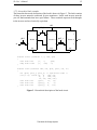
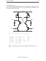
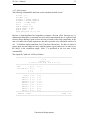
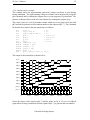
A latch is a two phase clocked register element. Figure 2 shows the transistor diagram
and the network description of the latch circuit. The circuit consists of three inverter
stages. Two of these stages are connected as a flipflop by phi2_l. The input signal is
clocked by phi1, whereas the output stage is clocked by phi2_r.
phi2_l
vdd
7
phi1
in
phi2_r
6
9
out
10
vss
network latch (terminal vdd, vss, phi1, phi2, out, in)
{
net {phi2, phi2_r, phi2_l}; /* equivalent nodes */
nenh w=8u l=4u
(9,
vss,
7);
nenh w=8u l=4u
(10,
vss,
out);
nenh w=8u l=4u
(6,
vss,
9);
nenh w=8u l=4u
(phi1,
in,
6);
nenh w=8u l=4u
(phi2_l, 6,
7);
nenh w=8u l=4u
(phi2_r, 9,
10);
ndep w=6u l=18u
(out,
out,
vdd);
ndep w=6u l=18u
(9,
vdd,
9);
ndep w=6u l=18u
(7,
7,
vdd);
}
Figure 2. Transistor diagram and network description of the latch circuit.
Note that the two terminals phi2_l and phi2_r are coalesced to one terminal named phi2
in the net declaration, for these terminals represented the same electrical node.
The Nelsis IC Design System
Sls User’s Manual
15
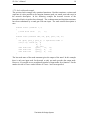
3.7.2 hierarchical latch example.
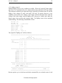
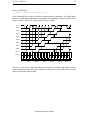
The hierarchical network description of the latch is shown in Figure 3. The latch consists
of three inverter networks connected by pass transistors. Inside each inverter network
you will find terminals that have equal names. These terminals represent feed-throughs
in the inverter and are electrically equivalent.
vdd
phi2_l
vdd
o
phi1
in
vdd
i
invert o
i
i
vss
6
7
o
vdd
i
o
phi2_r
invert o
9
i
i
9
i
invert o
10
i
vss
vss
network invert (terminal i, o, vdd, gnd)
{
nenh w=8u l=4u
(i,
o,
gnd);
ndep w=6u l=18u
(o,
vdd,
o);
}
network latch (terminal vdd, vss, phi1, phi2, out, in)
{
net {phi2, phi2_r, phi2_l}; /* equivalent nodes */
{inv[1..3]} invert (6, 9,
vdd, vss,
9, 7,
vdd, vss,
10, out, vdd, vss);
nenh w=8u l=4u
(phi1,
in,
6);
nenh w=8u l=4u
(phi2_l, 6,
7);
nenh w=8u l=4u
(phi2_r, 9,
10);
}
Figure 3. Hierarchical description of the latch circuit.
The Nelsis IC Design System
i
vss
out
Sls User’s Manual
16
3.7.3 latch with nand example.
The previous latch example only contained transistors. Besides transistors, resistors and
capacitors it is also possible to use function elements (ands, ors, nands, nors and exors) in
the network description. In the following example the network inverter of the
hierarchical latch circuit has been changed. The n-enhancement and depletion transistor
have been substituted by a nand gate with one input. The total network description is
now.
network invert (terminal i, o)
{
@ nand tr=5n tf=3n
(i,
}
o);
network latch (terminal vdd, vss, phi1, phi2, out, in)
{
net {phi2, phi2_r, phi2_l}; /* equivalent nodes */
{inv[1..3]} invert (6, 9,
9, 7,
10, out);
nenh w=8u l=4u
(phi1,
in,
6);
nenh w=8u l=4u
(phi2_l, 6,
7);
nenh w=8u l=4u
(phi2_r, 9,
10);
}
The last node name of the nand statement gives the output of the nand. In this example
there is only one input node for the nand, so only one node precedes the output node.
However, it is possible to use an arbitrarily number of input nodes for a function. For the
nand a rise time of 5 nsec. and a fall time of 3 nsec. have been specified.
The Nelsis IC Design System
Sls User’s Manual
17
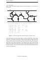
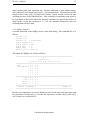
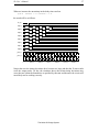
3.7.4 shift example.
Figure 4 shows the transistor diagram and the network description of a circuit which we
will call shift.
vdd
phi1
1
phi2
2
4
in
out
3
vss
network
{
nenh
ndep
nenh
cap
nenh
nenh
nenh
res
cap
}
shift (terminal vdd, vss, phi1, phi2, in, out)
w=6u
w=6u
w=8u
400f
w=8u
w=6u
w=6u
20k
150f
l=4u
l=10u
l=4u
(2,
l=4u
l=4u
l=4u
(4,
(out,
(in,
(1,
(phi1,
vss);
(phi2,
(3,
(vdd,
out);
vss);
vss,
1,
1,
1);
vdd);
2);
2,
vss,
4,
3);
4);
vdd);
Figure 4. Transistor diagram and network description of the shift circuit.
In the shift circuit, the inverted input signal is clocked by phi1 onto a large storage
capacitance. When phi1 becomes low and phi2 becomes high, the storage capacitance
shares its charge with the gate capacitance of the second inverter stage. Because the gate
capacitance is several times smaller then the storage capacitance, the gate will obtain the
same state as the storage capacitance. The second inverter stage consists of two
enhancement transistors with the upper transistor being saturated and acting as load for
the lower transistor. The resistor and capacitor on the output represent interconnection
resistance and capacitance.
The Nelsis IC Design System
Sls User’s Manual
18
3.7.5 flipflop example.
Figure 5 shows the transistor diagram and the network description of a flipflop circuit. In
this circuit the two nand circuit stages are cross coupled together by attaching the output
of one nand to an input of the other.
vdd
out[1]
out[2]
in[1]
in[2]
vss
network flipflop (terminal vdd, vss, in[1..2],
out[1..2])
{
nenh w=6u
l=4u
(in[1],
vss,
1);
nenh w=6u
l=4u
(out[1], 2,
out[2]);
nenh w=6u
l=4u
(in[2],
vss,
2);
nenh w=6u
l=4u
(out[2], 1,
out[1]);
ndep w=6u
l=20u (out[1], out[1], vdd);
ndep w=6u
l=20u (out[2], out[2], vdd);
cap 100f
(out[1], gnd);
cap 150f
(out[2], gnd);
}
Figure 5. Transistor diagram and network description of the flipflop circuit.
The Nelsis IC Design System
Sls User’s Manual
19
4. SIMULATION AND SIMULATION COMMANDS
4.1 Simulation Control Commands
The simulation control commands must reside in a separate file (the command file). This
file contains the signal descriptions of the network inputs and the commands which
specify options and output format.
TABLE 6. Syntax of the simulation control part.
iiiiiiiiiiiiiiiiiiiiiiiiiiiiiiiiiiiiiiiiiiiiiiiiiiiiiiiiiiiiiiiiii
sim_cmd_list
sim_cmd
set_cmd
signal_exp
value_exp
value
duration
fill_cmd
fill_vals
fill_val
def_cmd
def_minterms
def_minterm
def_in_val
def_out_val
print_cmd
plot_cmd
dump_cmd
initialize_cmd
dissip_cmd
option_cmd
option
= sim_cmd ( ";" | newline )
{ sim_cmd ( ";" | newline ) }.
= set_cmd | fill_cmd | def_cmd | print_cmd | plot_cmd
| dump_cmd | initialize_cmd | dissip_cmd | option_cmd | empty.
= set node_refs "=" signal_exp
| set node_refs ":" node_refs from string.
= value_exp { value_exp }.
= value [ "*" duration ].
= h | l | x | f | "(" signal_exp ")".
= integer | "˜".
= fill full_node_ref with fill_vals.
= fill_val { fill_val }.
= string | integer | f_float.
= define node_refs ":" identifier def_minterms.
= def_minterm { def_minterm }.
= def_in_val { def_in_val } ":" def_out_val.
= h | l | x | -.
= integer | identifier | $identifier.
= print node_refs.
= plot node_refs.
= dump at integer.
= initialize from string.
= dissipation [ node_refs ].
= option option { option }.
= simperiod "=" integer
| sigoffset "=" integer
| sigunit "=" f_float
| outunit "=" power_ten
| outacc "=" power_ten
| level "=" integer
| process "=" string
| tdevmin "=" f_float
| tdevmax "=" f_float
| step "=" ( on | off )
| print races "=" ( on | off )
The Nelsis IC Design System
Sls User’s Manual
node_refs
node_ref_item
full_node_ref
inst_name
node_ref
index_list
index
range
20
| maxldepth "=" integer
| only changes "=" ( on | off )
| disperiod "=" integer
| print devices "=" ( on | off )
| print statistics "=" ( on | off )
| maxpagewidth "=" integer
| vh "=" f_float
| vminh "=" f_float
| vmaxl "=" f_float
| initialize random "=" ( on | off )
| initialize full random "=" ( on | off )
| sta_file "=" ( on | off ).
= node_ref_item { node_ref_item }.
= full_node_ref | ",".
= [ "!" ] { inst_name "." } node_ref.
= identifier [ "[" index_list "]" ].
= integer | identifier [ "[" index_list "]" ].
= index { "," index }.
= integer | range.
= integer ".." integer.
Simulation commands are separated by a newline character or by a ";". So unlike with
the network description language, a newline character can not be used here as an
ordinary separator between symbols. However, a newline can be escaped as a command
separator by preceding it with a "\".
For an explanation of the non-literal terminals (e.g power_ten, f_float, etc.) the reader is
referred to the table "lexical constructions" in the network syntax description part in this
manual
Examples of node references (node_refs) in the commandfile are
cin 4, counter1.latch_a.112
total.submod[0..7,3].in[4..1]
with counter1, latch_a, total and submod[0..7,3] being instance names.
The explanation to the simulation commands is given in the next paragraphs.
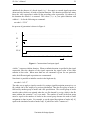
4.1.1 set command.
The set command describes the pulse signals that are applied to the network. A node
with a signal attached is by definition an input node. (In principle each node in the
network, including non-terminal nodes, may be used as an input node). The signal
expression that describes the signal in the set command consists of a sequence of value
expressions. A value expression specifies a logic level (i.e. l = 0, h = 1 and x =
The Nelsis IC Design System
Sls User’s Manual
21
undefined), the absence of a forced signal (i.e. f = free state) or a nested signal expression
(between curly brackets), all with an optional duration. The duration specifies how many
times the value expression is added to the preceding value expressions. By absence of
the duration the default 1 is assumed. The values l, h, x or f are pulse functions with
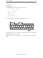
width is 1. So for the following set command:
set node1 = l*2 h*˜
the process of generation is shown in Figure 6.
l
............................................................................................
l*2
........................................................................................
h
............................................................................................
h*˜
l*2 h*˜
0
2
4
6
8
10
12
14
16
18
20
22
24
time
Figure 6. Construction of an input signal.
A tilde (˜) expresses infinite duration. When no infinite duration is specified in the signal
expression, after the duration of the signal expression the signal value of the node
remains its last value. When more than one set command is given for one particular
node, the different signal expressions are concatenated.
Note that it is possible to initialize a node in the high state by
set node1 = h*1 f*˜
The other way to apply a signal to a node is by using a signal description present in a .res
file (which can be the output of a previous simulation) Then the first group of nodes is
followed by another group of nodes and a file specification. The second group of nodes
must be nodes which were printed when the .res file denoted by string (which is the file
name without the extension ".res") was made. The number of nodes in the first group
must be equal to the number of nodes in the second group because the node to node
assignment is done in pairs. For example, to set the signal descriptions of nodes in[1..8]
equal to the simulation results of nodes out[1..8] which are in file "counter.res":
The Nelsis IC Design System
Sls User’s Manual
22
set in[1..8] : out[1..8] from "counter"
4.1.2 fill command.
With this command, state variables of function blocks can be initialized. To select a
particular state variable, the variable must be preceded by the (possibly hierarchical)
instance name of the function block. The type of the variable must correspond to the
type of the value that is assigned to it, with the convention that a string is used to specify
one or more character values.
Example:
fill ram1.mem[2..3, 0..3] with "OIOI" "OOII"
4.1.3 define command.
With this command, one can define new output values for the network based on certain
combinations of normal node values. For example, one may define the value of a state
variable based on the values of a set of nodes, or one may translate the values of a bundle
of nodes into an integer value. After the keyword "define", first the nodes are specified
that are used to determine the value of the new variable that is defined. Then, after a
colon, the name of the new variable is specified. Next, an arbitrary number of minterms
is defined. Each minterm consists of a number of node values (h, l, x or - for don’t care)
equal to the number of input nodes, followed by a colon and followed by the
corresponding value for the new variable. The output value may be an integer, an
identifier or a keyword starting with a "$". The simulator recognizes the following
keywords starting with a "$":
$dec
print decimal representation.
$oct
print octal representation.
$hex
print hexadecimal representation.
$sdec, $soct, $shex
idem, use left-most value as sign bit.
$tdec, $toct, $thex
idem, assume two-complements representation.
During simulation, the simulator traverses the list of minterms, starting with the first
minterm, to find a matching input combination. If it finds a matching input combination,
the output value of that minterm is used. If no matching combination of input values is
found, an X output value is used. The output values of the new variables can be printed
out by referring to them in a print command (see below).
The Nelsis IC Design System
Sls User’s Manual
23
Examples:
define a_1 a_2 :
- h :
l l
:
h l :
inputstate \
disabled \
nothing \
push
define in[1..8] : count8 \
- - - - - - - - : $dec
4.1.4 print command.
The print command specifies nodes that must be printed out. The sequence of the nodes
printed out is the same as specified in the print command. When a comma is specified in
the print command, an empty column is printed on that place in the output. When an "!"
sign is used before a node specification, the inverse value will be printed for that node.
The output will be printed in a file named to the network and tagged with the extension
".out". If the network name is longer than ten characters it will be truncated to ten
characters.
Examples:
print in[3..0], out[7..0], !notcarry,
print inv.i inv.o
The last print command will print node "i" and node "o" of the sub-cell with instance
name "inv". Apart from any network node, also the value of a user-defined variable may
be printed.
4.1.5 plot command.
For nodes that are specified in the plot command, a description of their approximating
voltage waveforms will be stored in the file "network.plt". To visualize these voltage
waveforms, an appropriate post-processor is required (lpsig or simeye).
Example:
plot cout sout inv1.in
4.1.6 dump command.
With the dump command, the state of a network can be dumped at any time. Together
with the initialize command this allows next simulations to start from that particular
point. This can be convenient for example when several simulations have to be done for
a circuit in which first a large number of registers has to be filled by means of shift
operations. The file in which the state will be dumped will be called "dump.time", where
time is the simulation time at which the dump is done. During one simulation more than
The Nelsis IC Design System
Sls User’s Manual
24
one dump may be executed.
Example:
dump at 200
4.1.7 initialize command.
The initialize command specifies a network state file that is used to initialize the network
state at the beginning of the simulation. The network state file must have been obtained
by using the dump command during a previous simulation.
Example:
initialize from "dump.200"
4.1.8 dissipation command.
The dissipation command allows the user to obtain estimated values for the dynamic
dissipation in the circuit. The information provided is only valid for networks that are
described at the transistor level. For the (network input) nodes that are given as an
argument to the dissipation command, the dynamic dissipation in Watts will printed in a
file called cell.dis. The total dissipation for the network can also be found there. By
using the option disperiod, it is possible to obtain an average dissipation for different
time intervals.
4.1.9 option command.
4.1.9.1 simperiod.
Specifies the end time (expressed in sigunit) of the simulation time interval. The start of
the simulation is always at t = 0. When simperiod is not specified, the simulation will
stop when the network has stabilized after the last input change.
(default simperiod = endless)
4.1.9.2 sigoffset.
Specifies the offset that is used for the signal specifications in the set command. That is,
each signal specification f(t) in the set command will be used as f(t-sigoffset) during
simulation.
(default sigoffset = 0)
4.1.9.3 sigunit.
Specifies (in seconds) the unit of signal duration in the set command, and the unit of each
other variable that denotes a time (e.g. the unit of simperiod).
The Nelsis IC Design System
Sls User’s Manual
25
(default sigunit = 1)
4.1.9.4 outunit.
Specifies the unit of time that will be used in the simulation output.
(default outunit = power_ten that is closest to sigunit)
4.1.9.5 outacc.
Specifies the unit of the least significant decimal of the time in the simulation output. It
must hold that outacc <= outunit.
(default outacc = outunit)
4.1.9.6 level.
Specifies the level of simulation. There are three simulation levels :
level 1
The simulator uses abstractions for transistors and nodes to determine logic states. The
conduction of n-enhancement and p-enhancement type transistors is always considered
then to be equal and much larger than the conduction of depletion transistors, and the
capacitances of all nodes are considered to be equal. A logic O or I state is only assigned
when the conducting path to an O or I state input has a much larger conduction than the
paths to other input nodes, or - with charge sharing - only when all nodes have the same
logic state. In other situations the X state is assigned.
level 2
With level 2, logic state determination is based on the actual parameters of transistors
(i.e. width and length) and interconnections (i.e. resistances and capacitances). In this
way the simulator is able to find the right states for circuits where charge sharing effects
occur between nodes with different capacitances and different states, and for circuits that
exploit a high-impedance/low-impedance resistance division effect between transistors of
the same type. In addition to the latter, at level 2 the simulator will also account for the
fact that n and p-enhancement transistors may be saturated. During simulation at level 2,
first for each node an analogue voltage is determined by means of charge sharing or
resistance division, and next a logic state is derived by means of a minimum voltage for
the high state (vminh) and a maximum voltage for the low state (vmaxl). When a
simulation is done at level 2, dimensions of transistors must be present in the network
and process information is used.
level 3
The simulator can also be used to simulate the timing of a network. Based on the
parameters of the transistors and the interconnections, also the delay times for the logic
The Nelsis IC Design System
Sls User’s Manual
26
state transitions are determined then. To find the delay times, the simulator uses
approximating piece-wise-linear voltage waveforms that are found by performing RC
constant calculations. At the start of a simulation at level 3, first a steady state of the
network is determined according to level 2. To simulate with timing, transistor
dimensions must be present in the network file and process information is used. Only at
level 3 the rise and fall delays of the function elements (nands, nors etc.) are taken into
account.
(default level = 1)
4.1.9.7 process.
Specifies the process file that contains the process information (e.g. transistor model
capacitances and resistances) which is used when simulation is done at level 2 or 3. First
the working directory is searched for this file. When it is not found there, the process
library directory is searched. In slsmod(3ICD) and [9] the syntax and semantics of a
process file is described.
(default process = "slsmod")
4.1.9.8 tdevmin,tdevmax.
By specifying minimum and maximum timing deviations it is possible to do a min-max
delay simulation at level 3. The delays of the logic state transitions are multiplied by
tdevmin and by tdevmax, to obtain a min-delay and a max-delay for each logic state
transition. For example, when a node normally changes from O to I after 10 ns., a
tdevmin = 0.6 and a tdevmax = 1.3 causes that the node will change from the O to the X
state after 6 ns., and to the I state after 13 ns. In this way it is possible to determine how
the final logical state of the simulated network depends on timing deviations due to
parameter variations or model accuracy (see also the flipflop example at the end of this
chapter). Note: strictly speaking tdevmin and tdevmax speed up and slow down the
minimum and maximum voltage waveforms that are being used by the simulator, and
delay times are affected only indirectly.
(default tdevmin = 1, tdevmax = 1)
4.1.9.9 step.
When step is on, the values of nodes that are specified by the print command, are printed
immediately after a change has occurred in the value of one of these nodes. In this way
the simulation of the network can be debugged by observing all logic state transitions
occurring on the printed nodes. It must be realized here that even during simulation
without timing (i.e. at level 1 or 2), the simulator always performs sequential simulation
steps to update logic states. When step is off, the values of the output nodes are printed
only after each new stabilization of the printed nodes at a particular time.
The Nelsis IC Design System
Sls User’s Manual
27
(default step = off)
4.1.9.10 print races.
When feedback loops are in the network (e.g. flipflops), there sometimes may occur
zero-delay oscillations during the simulation because of undecided races. The simulator
will automatically put the relevant nodes in the undefined state. Print races is on will
cause the simulator to give a list at the end of the simulation output, which shows where
and when these races appeared.
(default print races = on)
4.1.9.11 maxldepth.
With the maximum logic depth of the network (maxldepth), the simulator decides when
an oscillation because of undecided races is occurring (see option print races). When
maxldepth is specified too small the simulator will put nodes in the undefined state which
shouldn’t, and when it is much too large it will cause unnecessary long simulation times
when oscillations occur. However, the simulator detects that the maximum logic depth is
always less than the number of nodes in the circuit.
(default maxldepth = 100)
4.1.9.12 only changes.
By using only changes is on, in the output file only the logical values that have changed
will be printed. For an output signal which didn’t change a "." will be printed. In this
way it will be more easy to trace changing signals.
(default only changes = off)
4.1.9.13 disperiod.
Specifies the length of the time intervals (expressed in sigunit) for which the average
dissipation is printed (see the dissipation command).
(default disperiod = simperiod)
4.1.9.14 print devices.
Usually the only extra information that is given in the simulation output is the number of
nodes in the network. When print devices is on also the numbers of the different kinds of
devices (transistors, resistors and functions) are printed in the output file.
(default print devices = off)
The Nelsis IC Design System
Sls User’s Manual
28
4.1.9.15 print statistics.
When this option is on, simulation statistics like the number of simulation time points
and the number of logic events will be printed.
(default print statistics = off)
4.1.9.16 maxpagewidth.
Specifies the number of characters on a line in the output file. However, when
maxpagewidth >= 80 and all printed nodes will still fit on one line of 80 characters, the
number of characters on a line in the output file will be 80.
(default maxpagewidth = 132)
4.1.9.17 vh,vminh,vmaxl.
Simulation with level 2 or 3 requires a minimum stable voltage (vminh) for the I state, a
maximum stable voltage (vmaxl) for the O state, and a voltage vh for input nodes with
the I state (vl - for input nodes with the O state - is assumed to be 0 always). When a
stable voltage of a node is calculated to be between vmaxl and vminh, an X state will be
assigned to the node. Usually the variables vh, vminh and vmaxl are read from the
process file. But it is also possible to overwrite these values by specifying them in the
command file. Enlarging vmaxl for example, causes that nodes will be set to the O state
instead of the X state more often. It must hold that vmaxl < vh/2 < vminh.
(default vh, vminh, vmaxl are read from the process file)
4.1.9.18 initialize (full) random.
Normally, when simulating circuits with flipflops or memory cells that do not have a
reset input, some nodes in the circuit will remain uninitialized or X. When using the
option "initialize random", the simulator will randomly set these nodes at O or I.
Default, this initialization will be the same for different simulation runs of the same
network. However, when using the option "initialize full random", the result will be
different for each different simulation run. In general, the above options allow one to
reach some valid initial state at the beginning of a simulation, without first loading a state
over many clock cycles.
(default, initialize random = off and initialize full random = off)
4.1.9.19 sta_file.
Read additional commands from the file cell.sta if it exists. Typically, this option is used
to read in state variable definitions and print commands that are generated by an auxiliary
program.
(default, sta_file = off)
The Nelsis IC Design System
Sls User’s Manual
29
4.2 Examples
4.2.1 latch example.
The simulation control file of the latch circuit is as follows:
/* latch simulation commands */
set in
= (h*4 l*4)*2
set phi1 = (h*1 l*1)*˜
set phi2 = (l*1 h*1)*˜
set vdd = h*˜
set vss = l*˜
option simperiod = 10
print vdd vss phi1 phi2 in out
The set commands result in the following input pulse sequences:
in
phi1
phi2
0
2
4
6
8
10
12
14
16
18
20
22
24
time
The signals vdd and vss have a constant value during the simulation. The simulation
period is specified by option simperiod.
The node values of vdd, vss, phi1, phi2, in, out will printed in the file "latch.out" as
follows:
The Nelsis IC Design System
Sls User’s Manual
30
================================================================
S L S
version: 3.0
S I M U L A T I O N
R E S U L T S
================================================================
time
| v v p p i o
in 1e+00 sec | d s h h n u
| d s i i
t
|
1 2
================================================================
0 | 1 0 1 0 1 x
1 | 1 0 0 1 1 1
2 | 1 0 1 0 1 1
3 | 1 0 0 1 1 1
4 | 1 0 1 0 0 1
5 | 1 0 0 1 0 0
6 | 1 0 1 0 0 0
7 | 1 0 0 1 0 0
8 | 1 0 1 0 1 0
9 | 1 0 0 1 1 1
10 | 1 0 1 0 1 1
================================================================
network : latch
nodes : 10
================================================================
Remark that for the hierarchical latch example node "out" could also have been referred
to by "inv[3].o".
The Nelsis IC Design System
Sls User’s Manual
31
4.2.2 shift example.
The following command file has been used to simulate the shift circuit:
set vss = l*˜
set vdd = h*˜
set phi1 = (h*200 l*200)*2
set phi2 = (l*200 h*200)*2
set in
= l*400 h*400
set 3
= l*1 f*˜
option sigunit = 1n
option outacc = 10p
option level
= 3
print phi1 phi2 in, 2 3 out
Because a high-impedance/low-impedance resistance division effect between two nenhancement transistors (a saturated one and a and a non-saturated one) is exploited, and
because charge sharing is used to force the state of a node with a large capacitance to the
state of a node with a small capacitance, the shift circuit has to be simulated with level 2
or 3. To illustrate timing simulation, level 3 has been chosen here. We have to choose a
proper input unit and output accuracy with the options sigunit and outacc in order to see
the delays in the simulation output. Node 3 is initialized in the low state in this
command file.
The output file "shift.out" will be as follows:
================================================================
S L S
version: 3.0
S I M U L A T I O N
R E S U L T S
================================================================
time
| p p i
2 3 o
in 1e-09 sec | h h n
u
| i i
t
| 1 2
================================================================
0.00 | 1 0 0
1 0 1
200.00 | 0 1 0
1 0 1
200.14 | 0 1 0
1 1 1
205.68 | 0 1 0
1 1 0
400.00 | 1 0 1
1 1 0
407.85 | 1 0 1
0 1 0
600.00 | 0 1 1
0 1 0
600.07 | 0 1 1
0 0 0
607.07 | 0 1 1
0 0 1
================================================================
network : shift
nodes : 10
================================================================
The Nelsis IC Design System
Sls User’s Manual
32
4.2.3 flipflop example1.
With the flipflop circuit a race condition is possible. When in[1] and in[2] both change
state from O to I simultaneously, the voltage of both out[1] and out[2] will start falling.
The transistors with their gate connected to out[1] and out[2] will start to turn off, and the
falling of the voltages of out[1] and out[2] will stop. In practice however a race
condition exists because the voltage of one output will fall somewhat faster than the
voltage of the other output, and the flipflop will be driven in a stable state where the
fastest output is low and the other output is high. The flipflop circuit is first simulated
without timing. The following command file is used:
set vss = l*˜
set vdd = h*˜
set in[1..2]
= l*100 h*100
option sigunit = 1n
option outacc = 10p
option level
= 2
option step
= on
print in[1..2], out[1..2]
The output file "flipflop.out" will be as follows:
================================================================
S L S
version: 3.0
S I M U L A T I O N
R E S U L T S
================================================================
time
| i i
o o
in 1e-09 sec | n n
u u
| * *
t t
| 1 2
* *
| * *
1 2
|
* *
================================================================
0.00 | 0 0
x x
0.00 | 0 0
1 1
100.00 | 1 1
1 1
100.00 | 1 1
0 0
100.00 | 1 1
1 1
100.00 | 1 1
0 0
100.00 | 1 1
1 1
100.00 | 1 1
0 0
100.00 | 1 1
1 1
100.00 | 1 1
x x
================================================================
races occurred during simulation :
time nodes
100.00 out[1] out[2]
================================================================
network : flipflop
nodes : 7
================================================================
Because option step is on has been used in the command file, we see that the state of each
The Nelsis IC Design System
Sls User’s Manual
33
node is printed after each simulation step. Because simulation is done without timing,
out[1] and out[2] will change state to O at t = 100 simultaneously. The transistors will be
turned off then, node out[1] and out[2] will become I again, and the circuit will start
oscillating because of this undecided race. After a number of simulations steps equal to
the logic depth of the circuit (which the simulator assumes to be equal to the number of
nodes in the circuit) has occurred at t = 100, the simulator automaticly puts the
oscillating nodes in the X state.
4.2.4 flipflop example2.
A second simulation of the flipflop circuit is done with timing. The command file is as
follows:
set vss = l*˜
set vdd = h*˜
set in[1..2]
= l*100 h*100
option sigunit = 1n
option outacc = 10p
option level
= 3
option step
= on
print in[1..2], out[1..2]
The output file "flipflop.out" will be as follows:
================================================================
S L S
version: 3.0
S I M U L A T I O N
R E S U L T S
================================================================
time
| i i
o o
in 1e-09 sec | n n
u u
| * *
t t
| 1 2
* *
| * *
1 2
|
* *
================================================================
0.00 | 0 0
x x
0.00 | 0 0
1 1
100.00 | 1 1
1 1
108.53 | 1 1
0 1
================================================================
network : flipflop
nodes : 7
================================================================
Because now capacitances are used to find delay times for the logic state transitions, and
the capacitance of node out[1] is less than the capacitance of node out[2], node out[1]
will ’win the race’ and become O.
The Nelsis IC Design System
Sls User’s Manual
34
4.2.5 flipflop example3.
Finally a min-max delay simulation of the flipflop circuit is done. The min-max delay
has been specified by means of tdevmin and tdevmax. Node out[1] will now change
from I to O via the X state. During the interval that out[1] is X, out[2] also becomes X,
and the X state will result as the stable state for out[1] and out[2]. In this way the
simulator indicates that the final logic states depend on the timing, and that wrong logic
states can result when circuit parameters have 50 percent deviations.
The following command file was used for simulation:
set vss = l*˜
set vdd = h*˜
set in[1..2]
= l*100 h*100
option sigunit = 1n
option outacc = 10p
option level
= 3
option tdevmin = 0.5 tdevmax = 2
option step
= on
print in[1..2], out[1..2]
The output file "flipflop.out" will be as follows:
================================================================
S L S
version: 3.0
S I M U L A T I O N
R E S U L T S
================================================================
time
| i i
o o
in 1e-09 sec | n n
u u
| * *
t t
| 1 2
* *
| * *
1 2
|
* *
================================================================
0.00 | 0 0
x x
0.00 | 0 0
1 1
100.00 | 1 1
1 1
104.26 | 1 1
x 1
104.75 | 1 1
x x
================================================================
network : flipflop
nodes : 7
================================================================
The Nelsis IC Design System
Sls User’s Manual
35
4.2.6 random counter example
This example shows the approximating (min-max) voltage waveforms as used during
timing simulation. The approximating voltage waveforms can be inspected by using the
plot command, and by running the program simeye or the program lpsig afterwards. The
pictures as shown in this section have been obtained by running the program lpsig.
The circuit "rand_cnt" is an 8 bit random counter which uses a two-phase clock phi1 and
phi2 and which generates an 8 bit random number at the outputs out[0..7]. The command
file that has been used for the first simulation is as follows:
set
set
set
set
set
set
set
option
option
option
option
option
plot
in[0..7]
vss_r1 vss_r3
vdd_r3 vdd_r2 vdd_r1
phi1_r
phi2_r
p_ld_r
run_r
simperiod = 32
sigunit = 100n
outunit = 1n
outacc = 10p
level = 3
phi1_r phi2_r out[0..7]
=
=
=
=
=
=
=
h*˜
l*˜
h*˜
(h*1 l*1)* ˜
(l*1 h*1)* ˜
h*1 l*˜
l*1 h*˜
fb_in
The output for this simulation is shown below:
fb_in
out[7]
out[6]
out[5]
out[4]
out[3]
out[2]
out[1]
out[0]
phi2_r
phi1_r
0
500e-9
1000e-9
1500e-9
2000e-9
2500e-9
3000e-9
Notice the slopes on the signals out[0..7] and the spikes on fb_in. Fb_in is a feedback
signal which is being constructed from the signals out[0..7] to generate the next number.
The Nelsis IC Design System
Sls User’s Manual
36
Next we add the line
option
tdevmin = 0.7 tdevmax = 1.5
to the command file in order to perform a min-max delay simulation. The result shows
that now, during signal transitions, the minimum and maximum voltage waveform do no
longer coincide. Also, at fb_in more spikes become visible.
fb_in
out[7]
out[6]
out[5]
out[4]
out[3]
out[2]
out[1]
out[0]
phi2_r
phi1_r
0
500e-9
1000e-9
1500e-9
2000e-9
2500e-9
3000e-9
This way we are able to study the influence of parameter variations and model accuracy
on the simulation results and we for example see that spikes are possible on fb_in at the
end of each positive pulse of phi1.
The Nelsis IC Design System
Sls User’s Manual
37
When we increase the uncertainty in the delay times and use
option
tdevmin = 0.3 tdevmax = 1.9
the result will be as follows:
fb_in
out[7]
out[6]
out[5]
out[4]
out[3]
out[2]
out[1]
out[0]
phi2_r
phi1_r
0
500e-9
1000e-9
1500e-9
2000e-9
2500e-9
3000e-9
Notice that now the timing deviations have become too large and that the X state results
at all the output nodes. In fact, the simulator shows that when timing deviations may
occur that are within the boundaries as specified by tdevmin and tdevmax the circuit will
most likely not be working correctly.
The Nelsis IC Design System
Sls User’s Manual
38
5. TROUBLESHOOTING
In this chapter some suggestions are given to solve troubles which may occur during
simulation.
Trouble
Possible cause
syntax error
The statement or command did not obey the corresponding
syntax description as given in this manual.
no signal delay
You didn’t use simulation level 3.
The output accuracy (option outacc) is too large.
simulation never stops
You used a repetitive input signal and didn’t specify a
simulation end time (option simperiod).
races occurred
To find the cause of races: use option step = on and print all
nodes for which a race occurred. For more information,
see the flip flop simulation example and the explanation to
the option print races.
A (inappropriate) warning about the occurrence of races
may also be given if the real logic depth of the circuit is
more than the value of maxldepth. In that case, enlarge the
value of maxldepth.
wrong output values
You didn’t set all supply nodes (e.g. vdd and gnd) in the h
or l state.
You did forget to connect nodes by means of a net
statement.
For the circuit simulated right logic states can only be
simulated at level 2 or 3.
Some transistors have a wrong length or width.
If you can’t find it: recursively print the gate nodes of the
transistors that make up the wrong signal and/or use option
step = on.
Finally: when you use analog circuits like sense amplifiers
it might be possible that the simulator is not capable of
determining the right logic states. In that case a solution is
to replace those circuit parts by gate level descriptions.
The Nelsis IC Design System
Sls User’s Manual
39
References
1.
R.E. Bryant, ‘‘Switch level modeling of MOS Digital Circuits,’’ Proc. ICCC
Conf., pp. 68-71 (1982).
2.
R.E. Bryant, ‘‘A switch-level model and simulator for MOS digital systems,’’
IEEE Trans. Computers vol. C-33 pp. 160-177 (Feb. 1984).
3.
A.J. van Genderen, ‘‘Switch Level Timing Simulation,’’ M.S. Thesis (85-49),
Delft University of Technology (June 1985).
4.
P.M. Dewilde, A.J. van Genderen, and A.C. de Graaf, ‘‘Switch Level Timing
Simulation,’’ Proc. ICCAD Conf., pp. 182-184 (Nov. 1985).
5.
A.J. van Genderen, ‘‘SLS: An Efficient Switch-Level Timing Simulator Using
Min-Max Voltage Wavefroms,’’ Proc. VLSI 89 Conference, Munich, pp. 79-88
(August 1989).
6.
A. Vladimirescu, K. Zhang, A.R. Newton, D.O. Pederson, and A. SangiovanniVincentelli, SPICE Version 2G User’s Guide,, Univ of California, Berkeley (Aug.
1981.).
7.
O. Hol, ‘‘FUNC_MKDB: Function Blocks in SLS, USER’S MANUAL,’’ The
Nelsis IC Design System Documentation, Delft University of Technology (1988).
8.
N. Wirth,, ‘‘What can we do about the unnecessary diversity of notation for
syntactic definitions ?,’’ Comm. ACM 20 (Nov. 1977).
9.
A.J. Schooneveld,, ‘‘Determination of SLS Transistor Model Parameters,’’
taakverslag 87-84, Delft University of Technology, (April 1987).
The Nelsis IC Design System
CONTENTS
1. INTRODUCTION
.
.
.
.
.
.
.
.
.
.
.
.
.
.
.
.
.
.
1
.
.
.
.
.
.
.
.
.
.
.
2
.
.
.
.
.
.
.
.
.
.
.
.
.
.
.
.
.
.
.
.
.
.
.
.
.
.
.
.
.
.
.
.
.
.
.
.
.
.
.
.
.
.
.
.
.
.
.
.
.
.
.
.
.
.
.
.
.
.
.
.
.
.
.
.
.
.
.
.
.
.
.
.
.
.
.
.
.
.
.
.
.
.
.
.
.
.
.
.
4
4
6
6
6
12
13
14
4. SIMULATION AND SIMULATION COMMANDS
4.1 Simulation Control Commands
. . . . .
4.2 Examples . . . . . . . . . . . .
.
.
.
.
.
.
.
.
.
.
.
.
.
.
.
.
.
.
.
.
.
.
.
.
19
19
29
5. TROUBLESHOOTING .
.
.
.
.
.
.
.
.
.
.
.
.
.
.
.
.
38
References .
.
.
.
.
.
.
.
.
.
.
.
.
.
.
.
.
39
2. DESCRIPTION OF THE SLS-PACKAGE
3. THE DESCRIPTION OF NETWORKS
3.1 General conventions.
. . . .
3.2 Network Description
. . . .
3.3 Declarations . . . . . . .
3.4 Network Structure . . . . .
3.5 External Network Declaration . .
3.6 Global Nets . . . . . . .
3.7 Examples . . . . . . . .
.
.
.
.
.
.
.
.
.
.
.
.
.
-i-
LIST OF FIGURES
Figure 1. Information flow diagram of the SLS-package.
.
.
.
.
.
.
2
Figure 2. Transistor diagram and network description of the latch
circuit. . . . . . . . . . . . . . . .
.
.
.
.
.
14
Figure 3. Hierarchical description of the latch circuit. .
.
.
.
.
.
.
15
Figure 4. Transistor diagram and network description of the shift
circuit. . . . . . . . . . . . . . . .
.
.
.
.
.
17
Figure 5. Transistor diagram and network description of the flipflop
circuit. . . . . . . . . . . . . . . . .
.
.
.
.
18
Figure 6. Construction of an input signal.
.
.
.
.
21
.
- ii -
.
.
.
.
.
.
.
.
.
.
.
LIST OF TABLES
TABLE 1. Lexical constructions
.
.
TABLE 2. Syntax of the network part.
.
.
.
.
.
.
.
.
.
.
.
.
.
5
.
.
.
.
.
.
.
.
.
.
.
.
.
6
.
.
.
.
.
.
.
.
.
.
.
.
6
.
.
.
.
.
.
.
.
.
.
.
.
7
.
.
.
.
.
.
.
.
.
12
.
.
.
.
.
.
.
.
.
19
TABLE 3. Syntax of the declaration part.
TABLE 4. Syntax of the network body.
.
TABLE 5. Syntax of an extern network declaration.
TABLE 6. Syntax of the simulation control part.
- iii -
.