1
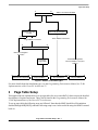
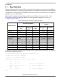
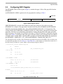
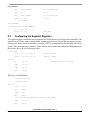
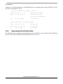
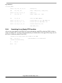
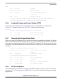
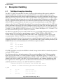
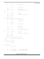
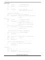
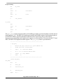
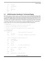
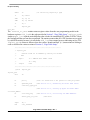
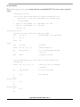
Freescale Semiconductor
Application Note
Document Number: AN2794
Rev. 1, 08/2010
Page Table Translation Setup
by
Networking and Multimedia Group
Freescale Semiconductor, Inc.
Austin, TX
This application note describes memory management unit
(MMU) page table setup for classic Power
Architecture®-based devices, such as the MPC755. The
simplest page table setup is discussed using the page table
translation mechanism to augment the block address
translation (BAT) registers. TLB miss, instruction storage
interrupt (ISI), data storage interrupt handling (DSI), and
on-demand paging are also discussed.
© 2010 Freescale Semiconductor, Inc. All rights reserved.
1.
2.
3.
4.
5.
Contents
Terminology . . . . . . . . . . . . . . . . . . . . . . . . . . . . . . . . 2
Types of Translation . . . . . . . . . . . . . . . . . . . . . . . . . . 2
Page Table Setup . . . . . . . . . . . . . . . . . . . . . . . . . . . . . 3
Exception Handling . . . . . . . . . . . . . . . . . . . . . . . . . 14
Revision History . . . . . . . . . . . . . . . . . . . . . . . . . . . . 23
Terminology
1
Terminology
The following terms are used in this document:
BAT
Block address translation mechanism. A set of registers that contain the
translation information and access privileges for blocks of memory.
DINK
Dynamic interactive nano kernel. This is a nano kernel and debugger for the
PowerPC systems.
DSI
Data storage interrupt (offset 0x300). This is the exception that a Power
Architecture-based processor takes when a data access cannot be translated by the
MMU.
ISI
Instruction storage interrupt (offset 0x400). This is the exception that a Power
Architecture-based processor takes when an instruction access cannot be
translated by the MMU.
Hash function
A mathematical construct that generates indexes (hash values) into a table to
minimize collisions.
Hash collision
A condition where two hash values index into the same table entry.
MMU
Memory management unit. This on-chip unit manages memory accesses on a
processor.
MSR
Machine state register. Contains information on various states of the processor.
Page
4 Kbytes of contiguous memory starting at a 4-Kbyte boundary
PTE
Page table entry. Contains the information on how a memory page may be
translated. PTEs are stored in memory and each one is 8 bytes in size.
PTEG
A group of 8 PTEs. The address of a PTEG should be aligned to a 64-byte
boundary.
SDR1
A register that defines the high-order bits for the physical base address and the size
of the page table.
SRx
Segment register used for page translation.
SRR1
Machine status save restore register 1. This register stores information when an
exception is taken.
TLB
Translation lookaside buffers. These on-chip storage entities store (cache)
recently accessed PTEs.
2
Types of Translation
Processor-generated memory accesses require address translation before they go out to the memory
subsystem. Instruction and data access translations are enabled through two bits (IR and DR, respectively)
in the machine state register (MSR).
When translation is disabled the processor is said to be in real addressing mode. In this mode all memory
is mapped one-to-one with effective memory/cache attributes (WIMG settings) of 0001 or 0011.
When translation is enabled, address translation is performed either through BATs or page tables and
TLBs. Figure 1 summarizes the translation types.
Page Table Translation Setup, Rev. 1
2
Freescale Semiconductor
Page Table Setup
0
31
Effective Address
Segment Descriptor
Located
(T = 1)
Address Translation Disabled
(MSR[IR] = 0, or MSR[DR] = 0)
Match with BAT Registers
(T = 0)
Block Address Translation
Page Address Translation
0
51
Virtual Address
Direct-Store Segment
Translation
Real Addressing Mode
Effective Address = Physical
Address
Look Up in
Page Table
0
31 0
Implementation-Dependent
31
Physical Address
0
31 0
Physical Address
31
Physical Address
Figure 1. Address Translation Types
For more details about the translation types, see the Programming Environments Manual for 32-Bit
Implementations of the PowerPC Architecture™.
3
Page Table Setup
This application note explains how to set up page tables for use as extra BATs. It does not provide detailed
descriptions of registers and terms. These can be found in the Programming Environments Manual for
32-Bit Implementations of the PowerPC™ Architecture.
To set up page tables the following steps are followed. Note that the MMU should be off (translation
disabled through MSR[IR,ID]) when the following setup is run. At the end of the setup, the MMU is turned
back on.
Page Table Translation Setup, Rev. 1
Freescale Semiconductor
3
Page Table Setup
3.1
Page Table Size
One page table entry (8 bytes) covers 4 Kbytes of memory. For example, to set up pages for sixteen Mbytes
of memory, 4096 entries (or 32 Kbytes of page table space) are required. However, due to the likelihood
of collisions in accessing the PTEs, a minimum of four times as much, or 16384 entries (or 128 Kbytes of
page table space), is recommended.
Table 1 lists the minimum recommended page table sizes for different memory sizes. The ‘x’ for
HTABORG gets filled with the upper address bits of the page table in memory (see Section 3.2,
“Configuring SDR1 Register”).
Table 1. Minimum Recommended Page Table Sizes
Settings for Recommended
Minimum
Recommended Minimum
Memory Covered
Number of
Mapped Pages
(PTEs)
Number of
PTEGs
HTABORG
(Maskable Bits
7–15)
HTABMASK
213
210
x xxxx xxxx
0 0000 0000
(217)
214
211
x xxxx xxx0
0 0000 0001
32 Mbytes (225)
256 Kbytes (218)
215
212
x xxxx xx00
0 0000 0011
(226)
(219)
216
213
x xxxx x000
0 0000 0111
217
214
x xxxx 0000
0 0000 1111
(221)
218
215
x xxx0 0000
0 0001 1111
4 Mbytes (222)
219
216
x xx00 0000
0 0011 1111
(223)
220
217
x x000 0000
0 0111 1111
Memory for Page
Tables
8 Mbytes (223)
16 Mbytes
64 Mbytes
64 Kbytes (216)
(224)
128 Kbytes
512 Kbytes
128 Mbytes (227)
256 Mbytes
1 Mbyte (220)
(228)
2 Mbytes
512 Mbytes (229)
1 Gbytes
(230)
8 Mbytes
2 Gbytes (231)
16 Mbytes (224)
221
218
x 0000 0000
0 1111 1111
(232)
(225)
222
219
0 0000 0000
1 1111 1111
4 Gbytes
32 Mbytes
Assuming the starting and ending memory addresses are in r3 and r4 registers respectively, the following
code stores the page table size to r6.
//calculate PT_size ((end-start)*8/4096)*4 or (end-start)/128
//minimum size of PT_size is 64 Kbytes
//PT_size is * 4 (to satisfy minimum
//requirement) (see table 7-22 of PEM for 32 bit manual)
sub
r6, r4, r3
srwi
r6, r6, 7
//div by 128 to get pt_size
rlwinm.
r8, r6, 20, 12, 31
//is PT_size >= 64 Kbytes
bne
cont
lis
r6, 0x10
//if not set to 64 Kbytes
cont:
Page Table Translation Setup, Rev. 1
4
Freescale Semiconductor
Page Table Setup
3.2
Configuring SDR1 Register
The HTABORG field of SDR1 register (Figure 2) contains the upper 16 bits of the page table location.
HTABORG
and HTABMASK of SDR1 register need to be programmed according to Table 1.
Reserved
0000 000
HTABORG
0
15 16
HTABMASK
22
23
31
Figure 2. SDR1 Register Format
SDR1[HTABMASK] is a mask with as many low-order ones as there are low-order zeros in the
HTABORG. For example, if the page table is located at 0x03A0_0000, HTABORG and HTABMASK
should be programmed to 0b0000_0011_1010_0000 and 0b0000_0000_0001_1111 respectively. The
relation between the HTABMASK, HTABORG and the size of the memory constrain the location of the
page table. The best way to satisfy these requirements is to place the page table at the upper end of the
physical memory. For example, for 64 Mbytes of memory, 512 Kbytes of memory is required for the page
tables (from Table 1). Placing the table at the upper end of the memory will yield page table base address
of 0x0400_0000 - 0x0008_0000 = 0x03F8_0000. An address of 0x03F8_0000 satisfies the requirement
that HTABORG = 0b0000_0011_1111_1000 and HTABMASK = 0b0000_0000_0000_0111.
The following PowerPC assembly code calculates the page table location and sets the SDR1. In the assembly code,
r6 contains the page table size (see Section 3.1, “Page Table Size”), and memSize is a function that returns (in r3)
the total memory available on a system. SDR1 is Special Purpose Register (SPR) 25.
//calculate PT_location (memSize-PT_size)
bl
memSize
sub
r3, r3, r6
//PT_loc=memSize-PT_size
//set up SDR1
xor
r9, r9, r9
ori
r9, r9, 0xffff
//set HTABORG of SDR1
rlwinm
r8, r9, 16, 0, 15
//r8=0xffff0000
and
r15, r3, r8
//r9=0x0000ffff
//set HTABMASK of SDR1
//in C it is:
//for(i=0x0000ffff;(sdr1_value&(i<<16)) && i>0;i>>=1);
htabmask:
rlwinm
r8, r9, 16, 0, 15
//i<<16
and.
r8, r8, r15
//c1=sdr1_value & i<<16
Page Table Translation Setup, Rev. 1
Freescale Semiconductor
5
Page Table Setup
beq
exit_htabmask
//if c1=0 then exit
cmpli
r9, 0
//i>0 ?
ble
exit_htabmask
//if i=<0 then exit
srwi
r9, r9, 1
//i>>=1
b
htabmask
exit_htabmask:
//now r9 should have the HTABMASK
3.3
or
r15, r15, r9
mtspr
25, r15
//set SDR1
Configuring the Segment Registers
The segment registers contain the virtual segment IDs (VSIDs) that are used for page table translation. The
upper 4 bits of effective address dictate which segment register to use. If more than one segment register
is being used, then each one needs to have a unique VSID. To accomplish this, the following code loads
up the VSIDs with consecutive numbers. In the code, r8 and r9 contain the starting and ending address of
the memory area to be covered by page tables.
//set up SRx
rlwinm
r3, r8, 4, 28, 31
//extract 4 MSBs
rlwinm
r4, r9, 4, 28, 31
//extract 4 MSBs
bl
set_srx
addi
r3, r3, 1
cmpw
r3, r4
ble
srx_set
srx_set:
//expects r8=value r9=sr index
Where set_srx is defined as:
//set srx registers
.global set_srx
set_srx:
cmpwi
r4, 0
beq
mtsr0
cmpwi
r4, 1
beq
mtsr1
//fill in the same sequence for SR2 up to SR14 here
cmpwi
r4, 15
beq
mtsr15
Page Table Translation Setup, Rev. 1
6
Freescale Semiconductor
Page Table Setup
mtsr0:
mtsr
0, r3
blr
mtsr1:
mtsr
1, r3
blr
//fill in the same sequence for SR2 up to SR14 here
mtsr15:
mtsr
15, r3
blr
3.4
Clearing the Page Tables
Before setting up the page tables, it is important to zero out the page table memory space first. This is
because page table entries are searched by looking at the valid bit of the entries and finding an invalid entry.
If the memory area is not cleared first, then false valid entries will create table collisions.
To clear the page table memory area, a simple store word instruction is used. Other means can be used as
well. Assuming r6 contains the table size in bytes and r7 contains the table location, the following
assembly code clears the page table memory.
//clear out page table memory
rlwinm
r6, r6, 30, 0, 31
mtctr
r6
xor
r8, r8, r8
subi
r7, r7, 4
//divide by 4
//pre-decrement r7
zero_out_pte:
3.5
stwu
r8, 4(r7)
bdnz
zero_out_pte
Constructing the Page Table
When looking for a page table entry for a page (4-Kbyte block), the processor uses a hash function, in
combination with the segment registers (for the VSID field of the virtual address) and the SDR1 register,
to construct a PTE group (PTEG) address (see Figure 3). In a similar fashion, when software sets up the
page tables, it should use the same algorithm to construct the PTEG address for a PTE. Once the PTEG is
calculated from the algorithm, then the first empty PTE (as indicated by the valid bit being cleared) is used
to store the translation information. If all the PTEs in a PTEG are already used (valid), then the second hash
value is generated from the first hash by inverting all the bits (one’s complement). To indicate that the PTE
is placed there using the second hash, the software sets the H bit in the upper PTE. The detailed assembly
code is described in subsequent sections. The process is repeated for each page of the memory area that is
covered by the page table.
Page Table Translation Setup, Rev. 1
Freescale Semiconductor
7
Page Table Setup
0
Virtual Page Number (VPN)
23 24
45
Virtual Segment ID
(24-bit)
52-Bit Virtual Address
29 30
39 40
51
API
(6-bit)
Byte Offset
(12-bit)
Page Index (16-bit)
(3 Bit)
(16-bit)
000
Hash Function
SDR1
0
67
15 16
xxxx xx . . . . . . 00
(16-bit)
22 23
0000000
31
0
8 9
18
Hash Value
(19-bit)
00 . . . . 011. . .1
(9-bit)
Mask
10 bits
9 bits
Base
Address
AND
PAGE TABLE
PTE0
OR
PTE7
8 bytes
PTEG0
0
67
(7-bit)
15 16
(9-bit)
25 26
(10-bit)
31
000000
(6 Bit)
PTEG Select
PTEGn
32-Bit Physical Address of Page Table Entry
64 Bytes
Lower PTE
Upper PTE
01
24 25 26
VSID
(24-bit)
V
31
API
(6-bit)
0
19
Physical (Real) Page Number
(RPN) (20-bit)
H
32-Bit Physical Address
23
25
000 R C
29
31
0 PP
WIMG
RPN (20-bit)
Byte Offset (12 bit)
Figure 3. Generation of Addresses for Page Tables
Page Table Translation Setup, Rev. 1
8
Freescale Semiconductor
Page Table Setup
The following sections detail how a PTE is loaded into the table.
3.5.1
Segment Register Selection and Loop Setup
PTEs are constructed for each page in the memory range covered. For each page we figure out which
segment register to use. Segment register is selected by the 4 upper bits of the effective address (there are
16 segment registers). The following source code sets up the loop for each page in the address range that
is to be covered and reads the appropriate segment register.
//loop for each 4k block of memory
load_PTEs:
cmpw
r3, r4
bge
check_low_memory
//figure out which sr we need
rlwinm
r8, r3, 4, 28, 31
//get_srx expects input in r8 and outputs to r13
get_srx
Where get_srx is:
/get srx registers
.global get_srx
get_srx:
cmpwi
r8, 0
beq
mfsr0
cmpwi
r8, 1
beq
mfsr1
//...repeat for mfsr2 up to mfsr15
mfsr0:
mfsr
r13, 0
blr
mfsr1:
mfsr
r13, 1
blr
//...repeat for sr2 up to sr15
3.5.2
Setting Up Upper and Lower PTEs
PTEs have the format shown at the bottom of Figure 3, with an upper word and a lower word. We set up
the PTE before we search in the table to find where to put it. The following code, which assumes SRx
Page Table Translation Setup, Rev. 1
Freescale Semiconductor
9
Page Table Setup
content in r13, effective address in r3 and WIMG bits in r5, sets up the upper word of the PTE in r11 and
the lower word of the PTE in r12.
//construct V/VSID/API for loading to PTE later
rlwinm
r11, r13, 7, 1, 24
//extract VSID from SRx
rlwimi
r11, r3, 10, 26, 31
//extract API from EA
//and insert in VSID/API reg
oris
r11, r11, 0x8000
//set Valid bit
//set up lower word of the PTE with EA=PA
3.5.3
rlwinm
r12, r3, 0, 0, 19
//extract RPN
rlwimi
r12, r5, 3, 25, 28
//insert WIMG
ori
r12, r12, 0x182
//R=C=1,PP=10
Generating the First Hash Value
The first hash value is generated by performing an exclusive OR of the 19 low-order bits of the VSID and
bits 4-19 of the effective address preceded by three 0s (see Figure 4).
Page Table Translation Setup, Rev. 1
10
Freescale Semiconductor
Page Table Setup
Primary Hash:
VA5
VA23
Low-Order 19 Bits of VSID (from Segment Register)
XOR
4
000
19
Page Index (Virtual Address bits 24–39 or Effective Address bits 4–19)
=
Hash Value 1
Output of Hashing Function 1
0
8
9
18
Secondary Hash:
0
18
Hash Value 1
One’s Complement Function
Output of Hashing Function 2
0
8
9
Hash Value 2
18
Figure 4. Hashing Functions for Page Tables
The assembly code that generates the hash1 value is below. The code assumes the effective address is in
r3 and the segment register contents are in r13. It stores the hash1 value into r14.
//hash1 = SRx[13-31] xor ( 0b000 || EA[4-19])
3.5.4
rlwinm
r14, r3, 20, 16, 31
//extract EA[4-19]
rlwinm
r12, r13, 0, 13, 31
//extract SRx[13-31]
xor
r14, r14, r12
//xor the two
Calculating the PTEG Address
The PTEG address is then generated according to the algorithm shown in Figure 3. The code for this part
of the algorithm is below. In this code, the SDR1 value is assumed to be contained in r15, and the hash1
value is stored in r15. At the end of this code, r9 holds the PTEG address.
//calculate PTEG address
//PTEG address = SDR1[0-6] ||
//
(SDR1[7-15] | (SDR1[23-31] & hash[13-21]))
//
|| hash[22-31] || 0b000000
Page Table Translation Setup, Rev. 1
Freescale Semiconductor
11
Page Table Setup
calculate_PTEG:
rlwinm
r12, r14, 22, 23, 31
//hash[13-21]
and
r12, r12, r15
//tmp1 = SDR1[23-31] & hash[13-21]
rlwinm
r8, r15, 16, 23, 31
//SDR1[7-15]
or
r12, r12, r8
//tmp2 = SDR1[7-15] | tmp1
xor
r9, r9, r9
//zero out PTEG address
rlwimi
r9, r15, 0, 0, 6
//insert SDR1[0-6] into PTE addr[0-6]
rlwimi
r9, r12, 16, 7, 15
//insert tmp2 into PTE addr[7-15]
rlwimi
r9, r14, 6, 16, 25
//insert hash[22-31] into
//PTE addr[16-25]
3.5.5
Searching for an Empty PTE location
After we have the address of the PTEG, we traverse through the eight PTEs within the PTEG to find an
empty (available) PTE. An empty PTE is identified by its valid bit (bit 0 of the upper PTE) being clear. In
this code, r9 holds the address of the PTEG.
//search for an entry within the 8 PTEs in the PTEG
subi
r9, r9, 8
//pre-decrement r9 for PTE search
//search and insert entry
li
r10, 8
mtctr
r10
Page Table Translation Setup, Rev. 1
12
Freescale Semiconductor
Page Table Setup
next:
lwzu
r8, 8(r9)
//load PTE
rlwinm. r8, r8, 1, 31, 31
//check valid bit
beq
//if we find an empty PTE then
exit_loop
// exit loop
bdnz
next
//otherwise continue
//if we get here then we did not find an empty entry in which case we generate
//2nd hash (see Section 3.5.7, “Generating the Second Hash Value”)
3.5.6
Loading the Upper and Lower Words of PTE
After we have successfully located an empty PTE location, we load the PTE we constructed in
Section 3.5.2, “Setting Up Upper and Lower PTEs,” to the empty table location.
exit_loop:
//we have found an empty PTE. Populate it for current EA
stw
r11, 0(r9)
//load upper word of PTE
stw
r12, 4(r9)
//load lower word of PTE
3.5.7
Generating the Second Hash Value
If there is no empty PTE within the PTEG in the previous section, a second hash is calculated. The second
hash is a one’s complement of the first hash (see Figure 4). The following code first checks if second hash
has already been attempted (indicated by the H bit in the PTE (contained in r11) that we are trying to insert
to the table). If not, then it performs the second hash; otherwise, it flags an error. The first hash is assumed
to be in r14.
//Check to see whether second hash already tried
rlwinm. r12, r11, 26, 31, 31
//check for H bit in V/VSID/API
// register
bne
return_error
//if set, flag an error
//if second hash not tried, then try second hash
3.5.8
xoris
r14, r14, 0xffff
//ones-complement hash1
xori
r14, r14, 0xffff
//r14=hash2
ori
r11, r11, 0x40
//set H bit in V/VSID/API register
b
calculate_PTEG
// to indicate 2nd hash
Set Up Completion
The preceding setup is performed for each page in the address range covered. If an error is encountered
(see Section 3.5.7, “Generating the Second Hash Value”), an error is returned to the calling routine and the
program exits.
Page Table Translation Setup, Rev. 1
Freescale Semiconductor
13
Exception Handling
4
Exception Handling
4.1
TLB Miss Exception Handling
The MPC755, MPC744x, and MPC745x have a feature in which software table search is enabled or
disabled; in MPC603e and other processors with the MPC603e core, hardware table search is not
supported. When software table search is enabled and memory access does not hit on the on-chip TLBs or
BATs, the processor generates one of the TLB exception handlers. Instruction TLB miss exception (offset
0x1000) is generated when an instruction access can’t be translated; data TLB load miss exception (offset
0x1100) is generated when a data load access cannot be translated and data TLB store miss exception
(offset 0x1200) is generated when a data store access can’t be translated by the on-chip TLBs or BAT
registers or the C bit in a PTE needed to be updated. The system software needs to search for a PTE from
memory and load an on-chip TLB as well as update the R and C bits of the PTE. For details please read
the respective user’s manuals for the processors. The exception handling routines are described in Figures
5-16 and 5-17 of the MPC603e RISC Microprocessor User’s Manual and Figures 5-33, 5-34 and 5-35 of
the MPC7450 RISC Microprocessor Family User’s Manual.
The MPC603e (and other processors with the MPC603 core) set the MSR[TGPR] bit after taking a TLB
miss exception. This bit maps four special purpose registers TGPR0-TGPR3 to GPR0-GPR3.
TGPR0-TGPR3 are accessed through GPR0-GPR3 and are used as temporary registers for use in the
exception handler. With the TGPR bit set, software cannot access GPR0-GPR3. Using GPR4-GPR31
results in indeterminate behavior. For inter-processor compatibility purposes this feature was not used in
writing the code below. For code compactness (i.e. to get the same code to work on all the processors), the
MSR[TGPR] bit is cleared immediately after a TLB miss exception as follows:
mfmsr
r3
oris
r3, r3, 0x0002
xoris
r3, r3, 0x0002
mtmsr
r3
R3 (GPR3) should be saved after the MSR bit is cleared. Saving it before the bit is cleared only results in
saving the TGPR3 register.
The following code shows the implementation of the exception handling for the TLB miss exception.
Before it gets to this routine, r23 is loaded with the contents of the DMISS register (or TLBMISS for
MPC744x/MPC745x), r24 is loaded with DCMP (or PTEHI for MPC744x/MPC745x), and r25 is loaded
with RPA (or PTELO for MPC744x/MPC745x). See the processor’s user’s manual for details on what
these registers mean. These registers are also discussed in TLB Translation for the MPC603e/MPC755
(AN2795) and TLB Translation for the MPC745x/MPC744x (AN2796).
//ITLB miss exception for processors with software table search
// enabled - in these routines ex_type holds the exception offset
do_TLB:
mr
r3, r23
//get EA of miss
li
r4, 1
//try 1st hash first
bl
get_pteg
//get pteg address
Page Table Translation Setup, Rev. 1
14
Freescale Semiconductor
Exception Handling
mr
r5, r24
//get cmp value
li
r4, 8
//load counter
mtctr
r4
//load counter
subi
r3, r3, 8
//pre-decrement pteg pointer
lwzu
r4, 8(r3)
//get pte
cmpw
r4, r5
//compare with compare value
beq
got_pte
bdnz
next1
next1:
//if we get here first, then hash has failed
mr
r3, r23
//get EA of miss
li
r4, 2
//try 2nd hash
bl
get_pteg
mr
r5, r24
//get cmp value
li
r4, 8
//load counter
mtctr
r4
//load counter
subi
r3, r3, 8
//pre-decrement pteg pointer
lwzu
r4, 8(r3)
//get pte
cmpw
r4, r5
//compare with compare value
beq
got_pte
bdnz
next2
next2:
// if we get here, then both hashes have failed
b
quit_gracefully
//page fault case
got_pte:
//read lower pte from memory
lwz
r5, 4(r3)
//set R bit in pte
ori
r5, r5, 0x100
lis
r4, ex_type@h
//
get high order address
ori
r4,r4, ex_type@l
//
get low order address
Page Table Translation Setup, Rev. 1
Freescale Semiconductor
15
Exception Handling
lwz
r4,0(r4)
//
load the exception type
cmpwi
r4, 0x1000
// is this an ITLB miss?
bne
ignore_G_bit
// if not (i.e. this is
// DTLBS or DTLBL), then ignore G bit
//check G bit for ITLB misses
rlwinm.
r6, r5, 29, 31, 31//check G bit for ITLB miss
bne
quit_gracefully
//if G bit set, then it is a page protection
//violation
ignore_G_bit:
cmpwi
r4, 0x1200
// is this a DTLB Store miss?
bne
cont_TLB_handle
// if not DTLBS (i.e. this is
// DTLBL), then don't check/set C bit
// also don't check for page violations
rlwinm.
r6, r5, 25, 31, 31//check C bit
bne
skip_pte_update
//if set,then no need to check/update
// other bits of pte
//check for page violations (PP bits) for DTLB store miss
rlwinm.
r4, r5, 31, 31, 31//if PP=0x check SRR1[KEY]
beq
check_SRR1_key
rlwinm.
r4, r5, 0, 30, 31 //if PP=11, then it is page protection
cmpwi
r4, 0x3
beq
quit_gracefully
//violation
//set C bit in pte for DTLBS (DTLB store)
ori
r5, r5, 0x80
//there is no violation, continue
b
cont_TLB_handle
check_SRR1_key:
mfsrr1
r4
rlwinm.
r4, r4, 13, 31, 31
beq
quit_gracefully
//page protection violation if
Page Table Translation Setup, Rev. 1
16
Freescale Semiconductor
Exception Handling
// PP=0x and SRR1[KEY]=1
cont_TLB_handle:
//store pte to page table in memory & rpa
stw
r5, 4(r3)
//dcbf
0, r3
skip_pte_update:
//if this is 603e or 755 store to rpa otherwise store to ptelo
mfspr
r9,287
//Only use upper half of PVR
rlwinm
r9,r9,16,16,31
cmpli
cr0,0,r9,0x6
beq
store_to_rpa
cmpli
0,0,r9,0x0008
beq
store_to_rpa
cmpli
cr0,0,r9,0x81
beq
store_to_rpa
cmpli
cr0,0,r9,0x8081
beq
store_to_rpa
mtspr
ptelo, r5
b
skip_rpa
//Is this an MPC603? (i.e. PVR = 0x0006_nnnn)
//Is this MPC750/MPC755?
//Is this an MPC8240? (i.e. PVR = 0x0081_nnnn)
//Is this an MPC8245? (i.e. PVR = 0x8081_nnnn)
store_to_rpa:
mtspr
rpa, r5
skip_rpa:
//get ready for tlbld/tlbli
mr
r3, r23
//get miss address
//if this is an ITLB miss, then do tlbli otherwise do tlbld
lis
r4, ex_type@h
//
get high order address
ori
r4,r4, ex_type@l
//
get low order address
lwz
r4,0(r4)
//
load the exception type
cmpwi
r4, 0x1000
// is this a DTLB load miss?
Page Table Translation Setup, Rev. 1
Freescale Semiconductor
17
Exception Handling
bne
do_tlbld
sync
tlbie
r3
//invalidate
r3
//load
sync
tlbli
sync
b
cont_restore
do_tlbld:
sync
tlbie
r3
//invalidate
r3
//load
sync
tlbld
sync
The get_pteg routine returns the address of the PTEG given data or instruction address and the desired
hash function (1 or 2). The MPC603e implements HASH1 and HASH2 registers for this purpose (that is,
to hold PTEG address for first-hash and second-hash values respectively), but, for the sake of
inter-processor compatibility and simplicity, the registers were not used here. Likewise, the MPC755 and
MPC745x/MPC744x implement similar registers. The get_pteg routine is provided next.
//////////////////////////////////////////////////////////
// get_pteg
//
Returns the pteg location for a given address and
//
either the first or second hash
//
input:
//
r4 = 1 or 2 to indicate desired hash
//
output:
r3 = pteg address
//
uses:
r17
r3 = effective address
/////////////////////////////////////////////////////////
.global get_pteg
get_pteg:
mflr
r17
bl
setup_upm
bl
translation_off
bl
generate_hash
cmpwi
r4, 1
Page Table Translation Setup, Rev. 1
18
Freescale Semiconductor
Exception Handling
bnel
flip_hash
bl
calculate_pteg
mr
r3, r9
bl
restore_msr
mtlr
r17
blr
4.2
DSI/ISI Exception Handling for On-Demand Paging
DSI or ISI exception occurs for a memory access that cannot be translated through BATs and page tables.
For on-demand paging, a PTE is allocated for the missing address at run time after taking the DSI or ISI
exception. The exception handler needs to find a spot for the new PTE in the page table. If there is no free
PTE in all the 16 PTE locations (8 generated from the first hash and 8 from the second), an entry is cast
out from the table. To minimize memory activity, a PTE (and a corresponding page) that is not modified
is selected as a victim PTE to be cast out. If all the 16 PTEs are modified, the last one is flushed from
memory to disk. The source code to do the exception handling for DINK is shown below.
// On-demand page:
//
If this is a DSI exception in user code, allocate a page table
//
translation for the exception on the fly and continue.
//
if we get to this point of the program we have run into exception while
//
running user code
#ifdef ON_DEMAND_PAGE
mfdar
r3
li
r4, 0x0fff
andc
r3, r3, r4
//setup translation for current page
//start addr = rounded down to page boundary
//check if current page is within the memory size
lis
r4, memSize@h
ori
r4, r4, memSize@l
lwz
r4, 0(r4)
cmpw
r3, r4
bgt
quit_dsi
//if greater than memSize quit
addi
r4, r3, 0x1000
//end addr = srr0+4k
li
r5, 0
//wimg=0
bl
pte_load
cmpwi
r3, 1
bne
quit_gracefully
//pte_load success
Page Table Translation Setup, Rev. 1
Freescale Semiconductor
19
Exception Handling
mfdar
r3
//on failure try replacing a page
li
r4, 0x0fff
andc
r3, r3, r4
addi
r4, r3, 0x1000
li
r5, 0
bl
replace_pte
quit_dsi:
The restore_to_user routine restores register values from the user programming model to the
hardware registers. PTE_load is the code provided in Section 3, “Page Table Setup.” replace_pte is
similar to pte_load with the main difference that it looks for unmodified PTE within 16 PTEs: 8 from
the first hash and the rest from the second hash. The routine assumes that all 16 PTE locations are occupied
by valid PTEs mainly because it is called after PTE_load has returned an error indicating no free PTE.
replace_pte is written as follows where the various “branch and link” (bl) instructions are linking to
code as described in various sections of Section 3, “Page Table Setup.”
//////////////////////////////////////////////////////////
// replace_pte
//
Creates a PTE for an address by casting out another
//
//
PTE.
input:
//
//
r3 = address that needs a PTE
r4 = wimg
output:
none
//////////////////////////////////////////////////////////
.global
replace_pte
replace_pte:
mflr
r17
bl
prolog
//turn off translation & set pointer to user prog model
bl
generate_hash
//see Section 3.5.3, “Generating the First Hash Value”
bl
construct_upper_pte
//see Section 3.5.2, “Setting Up Upper and Lower PTEs”
calculate_PTEG2:
bl
calculate_pteg
//see Section 3.5.4, “Calculating the PTEG Address”
bl
search_pteg_for_cast
cmpwi
r8, 0
bne
cont_1sthash2
//see below
Page Table Translation Setup, Rev. 1
20
Freescale Semiconductor
Exception Handling
//try 2nd hash
bl
flip_hash
//see Section 3.5.7, “Generating the Second Hash Value”
b
calculate_PTEG2
cont_1sthash2:
cmpwi
r8, 1
bne
populate
//see below
//if we get here all 16 PTEs are valid, and modified.
We need
//to flush out the last of these 16 PTEs to (simulated) disk
//extract lower PTE
lwz
r6, 4(r9)
//extract real page address (don't know how I can get the effective
//
or virtual page address since I don't have the hash value).
//
When we flush, we should translate the real page address to
//
virutal (effective) address
rlwinm
r6, r6, 0, 0, 19
//flush page
//Now we flush this modified page to disk
bl
flush_page_to_disk
//this depends on system (not implemented)
populate:
//populate the pte for the new page
mr
r5, r4
bl
populate_pte
bl
epilog
mtlr
r17
//turn on translation
blr
Page Table Translation Setup, Rev. 1
Freescale Semiconductor
21
Exception Handling
The search_pteg_for_cast routine looks for an unmodified PTE. The source code is provided
below:
//search pteg for cast
// This is the same as search_pteg but instead of searching for an
//
empty entry it looks for an unchanged (C bit cleared) entry
//
for replacement
//
input:r9 = pteg address, r11 = upper PTE, r14 = hash
//
output:r9 = pte address, r8 = 1 on error
//
uses:r10, r12
search_pteg_for_cast:
//search for an entry within the 8 PTEs in the PTEG
subi
r9, r9, 8
//pre-decrement r9 for PTE search
li
r10, 8
mtctr
r10
lwzu
r8, 8(r9)
//load PTE
rlwinm.
r8, r8, 25, 31, 31
//check changed bit
beq
pteg_success2
//if we find unchanged PTE then
next2:
// exit loop
bdnz
next2
//otherwise continue
//we have exhausted the list. Let's see if we have already tried
//second hash
rlwinm.
r12, r11, 26, 31, 31
//check for H bit in V/VSID/API
// register
bne
pteg_failure2
//if set flag an error
li
r8, 0
//try 2nd hash
blr
pteg_failure2:
li
r8, 1
blr
pteg_success2:
li
r8, 2
blr
Page Table Translation Setup, Rev. 1
22
Freescale Semiconductor
Revision History
The routine has three return values. On successfully finding an unmodified page, it returns a 2. If the first
hash fails, it returns a 0. If both the first and second hashes fail, it returns a 1. In all cases, the routine also
returns a pointer to the victim PTE in r9.
5
Revision History
Table 2 provides a revision history for this application note.
Table 2. Document Revision History
Rev.
Number
Date
1
08/2010
In Section 4.2, “DSI/ISI Exception Handling for On-Demand Paging,” changed mfsrr0 to mfdar.
0
10/2004
Initial public release
Substantive Change(s)
Page Table Translation Setup, Rev. 1
Freescale Semiconductor
23
How to Reach Us:
Home Page:
www.freescale.com
Web Support:
http://www.freescale.com/support
USA/Europe or Locations Not Listed:
Freescale Semiconductor, Inc.
Technical Information Center, EL516
2100 East Elliot Road
Tempe, Arizona 85284
1-800-521-6274 or
+1-480-768-2130
www.freescale.com/support
Europe, Middle East, and Africa:
Freescale Halbleiter Deutschland GmbH
Technical Information Center
Schatzbogen 7
81829 Muenchen, Germany
+44 1296 380 456 (English)
+46 8 52200080 (English)
+49 89 92103 559 (German)
+33 1 69 35 48 48 (French)
www.freescale.com/support
Information in this document is provided solely to enable system and software
implementers to use Freescale Semiconductor products. There are no express or
implied copyright licenses granted hereunder to design or fabricate any integrated
circuits or integrated circuits based on the information in this document.
Freescale Semiconductor reserves the right to make changes without further notice to
any products herein. Freescale Semiconductor makes no warranty, representation or
guarantee regarding the suitability of its products for any particular purpose, nor does
Freescale Semiconductor assume any liability arising out of the application or use of
any product or circuit, and specifically disclaims any and all liability, including without
limitation consequential or incidental damages. “Typical” parameters which may be
provided in Freescale Semiconductor data sheets and/or specifications can and do
vary in different applications and actual performance may vary over time. All operating
parameters, including “Typicals” must be validated for each customer application by
customer’s technical experts. Freescale Semiconductor does not convey any license
Japan:
Freescale Semiconductor Japan Ltd.
Headquarters
ARCO Tower 15F
1-8-1, Shimo-Meguro, Meguro-ku
Tokyo 153-0064
Japan
0120 191014 or
+81 3 5437 9125
[email protected]
under its patent rights nor the rights of others. Freescale Semiconductor products are
Asia/Pacific:
Freescale Semiconductor China Ltd.
Exchange Building 23F
No. 118 Jianguo Road
Chaoyang District
Beijing 100022
China
+86 10 5879 8000
[email protected]
claims, costs, damages, and expenses, and reasonable attorney fees arising out of,
For Literature Requests Only:
Freescale Semiconductor
Literature Distribution Center
1-800 441-2447 or
+1-303-675-2140
Fax: +1-303-675-2150
LDCForFreescaleSemiconductor
@hibbertgroup.com
Document Number: AN2794
Rev. 1
08/2010
not designed, intended, or authorized for use as components in systems intended for
surgical implant into the body, or other applications intended to support or sustain life,
or for any other application in which the failure of the Freescale Semiconductor product
could create a situation where personal injury or death may occur. Should Buyer
purchase or use Freescale Semiconductor products for any such unintended or
unauthorized application, Buyer shall indemnify and hold Freescale Semiconductor
and its officers, employees, subsidiaries, affiliates, and distributors harmless against all
directly or indirectly, any claim of personal injury or death associated with such
unintended or unauthorized use, even if such claim alleges that Freescale
Semiconductor was negligent regarding the design or manufacture of the part.
Freescale, the Freescale logo, and PowerQUICC, , are trademarks of
Freescale Semiconductor, Inc. Reg. U.S. Pat. & Tm. Off. The Power
Architecture and Power.org word marks and the Power and Power.org logos
and related marks are trademarks and service marks licensed by
Power.org.
© 2010 Freescale Semiconductor, Inc.