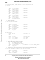
1
Freescale Semiconductor
AN2489/D
Rev. 0.1, 6/2003
Freescale Semiconductor, Inc...
Upgrading Software from
MPC7451 to
MPC7455 or MPC7457
Maurie Ommerman
CPD Applications
risc10@
email.mot.com
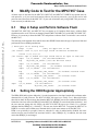
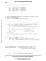
This document describes the process of modifying source code, software changes, for
upgrading from a MPC7450/MPC7451 to an MPC7455 or MPC7457, using the DINK32
source code as an example. The MPC7450, MPC7451, MPC7455, and MPC7457 are
PowerPC™ microprocessors. The MPC7451 has the same functionality as the MPC7450 and
any differences in data regarding bus timing, signal behavior, and AC, DC, and thermal
characteristics are detailed in the hardware specifications. Note that because the MPC7450
and MPC7451 have the same functionality they are used interchangeably through-out the
documentation and code.
The following topics are addressed:
Topic
Page
Section 1, “Introduction”
1
Section 2, “What are the Steps?”
2
Section 3, “Step 1: Add Processor Version Register (PVR) Definitions”
2
Section 4, “Step 2: Set DINK CPU Information and the PLL Table”
3
Section 5, “Step 3: Set the L3 Cache Bits”
6
Section 6.1, “Step 4: Setup and Perform Software Flush”
9
Section 7, “Step 5: Block Address Translation Registers (BATs) for the MPC7455 and
MPC7457”
11
Section 8, “Step 6: Setting Special Purpose Registers (SPRs)”
12
Section 9, “Conclusion”
16
Section 10, “Revision History”
16
Appendix A, “Complete Code Examples”
18
1
Introduction
This document describes the changes required in software to upgrade from an
MPC7450/MPC7451 to an MPC7455 or MPC7457. A general description of the changes is
given followed by some code snippets from DINK32, see Section 4.1, “CPU Information,” to
illustrate the differences. Some familiarity with DINK32 may be required to understand all the
code snippets.
•
•
“Step 1: Add Processor Version Register (PVR) Definitions,” shows the PVR setting.
“Step 2: Set DINK CPU Information and the PLL Table,” discusses the PLL settings.
© Freescale Semiconductor, Inc., 2004. All rights reserved.
For More Information On This Product,
Go to: www.freescale.com
Freescale Semiconductor, Inc.
Terminology
•
•
•
•
1.1
“Step 3: Set the L3 Cache Bits,” discusses the cache bit settings.
“Step 4: Setup and Perform Software Flush,” discusses the settings that do not change from the
MPC7450, MPC7455, to MPC7457, but may need to be detected.
“Step 5: Block Address Translation Registers (BATs) for the MPC7455 and MPC7457,” discusses
enabling the additional four BATs.
“Step 6: Setting Special Purpose Registers (SPRs),” discusses the L3 cache input timing control
register (L3ITCR0) setting.
Terminology
The following terms are used in this document:
Freescale Semiconductor, Inc...
•
•
•
•
•
•
•
•
•
2
DINK32—A small operating system (OS) debugger for the Sandpoint evaluation board.The
executable, user’s manual, and some source code are available on the Motorola web site. Search for
“DINK32” on the Motorola home page:www.mot.com/semiconductors.
BAT—Block Address Translation register, used to define large blocks of memory.
DDR—Dual Data Rate SDRAM
PLL—Phased-Lock Loop. A set of pins on the processor determine the divider to use for various
frequency settings. The PMC has a set of switches that can manipulate the pins on the processor to
allow various frequency settings to be configured at start up time.
PMC—PCI Mezzanine Card
RAM—Random Access Memory
SPR—Special Purpose Register
SDRAM—Synchronous Dynamic RAM
SRAM—Static RAM
What are the Steps?
To upgrade support from the MPC7450 to the MPC7455 and then the MPC7457, DINK32 source code was
changed as follows:
•
•
•
•
•
Added Processor Version Register (PVR) definitions
Defined the L3 cache settings
Performed a software flush
Encoded the phased-lock loop (PLL) settings
Established the hardware implementation-dependent register (HID0) settings.
In addition the AltiVec settings and the L3 cache input timing control register (L3ITCR0), a special purpose
register (SPR 984), are all discussed and the code is shown.
3
Step 1: Add Processor Version Register
(PVR) Definitions
Each Motorola processor has a unique read only register known as the PVR. Software that needs to
differentiate between the various processors must test for this PVR value. DINK32 is general purpose
software that determines which processor the software is running on via the PVR. DINK32 has a definition
2
Upgrading Software from MPC7451 to MPC7455 or MPC7457
For More Information On This Product,
Go to: www.freescale.com
Freescale Semiconductor, Inc.
CPU Information
for all the PVRs for the processors. DINK32 supports the PVR for the MPC7450, MPC7455, and
MPC7457.
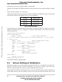
The PVR value for the:
•
•
•
MPC7450 is 0x8000
MPC7455 is 0x8001
MPC7457 is 0x8002.
The MPC7457’s PVR is defined in DINK32’s config.h file and is defined as:
Freescale Semiconductor, Inc...
#define PVR_7457
-32766
// 0x8002
The gcc compiler does not accept any 16 bit value where bit 0 is a 1
(0x8002 = 0b1000_0000_0000_0010). So, for any instruction that expects
a 16 bit value, such as immediate instructions, a value of 0x8002 will get
an error. However, gcc does accept the negative decimal equivalent, which
in this case is -32766 (-32766 = 0x8002 = 0b1000_0000_0000_0010).
Processor
PVR
MPC7450
0x8000
MPC7455
0x8001
MPC7457
0x8002
Figure 1. PVR Designators
4
Step 2: Set DINK CPU Information and the
PLL Table
In order for the software to behave properly with each processor, DINK32 must understand the attributes of
each device it supports. These attributes include, the name that is printed out on the splash screen, the PVR,
cache size, BAT attributes, floating point availability, AltiVec availability, and others. In addition, DINK32
must understand the hardware characteristics of each processor as described in the hardware specifications
for that device. DINK32 must know the core frequency for each processor that it supports. It uses an
algorithm that computes the core frequency from the known bus frequency and the PLL table
information.The following section provides details on how DINK32 sets the attributes for each specific
processor.
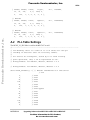
4.1
CPU Information
DINK32 uses a cpuinfo table to define the various attributes of each device. This table existed before the
MPC745x, and is used to define all known processors. The entry for the MPC7455 and MPC7457 is new in
this table, the MPC7450/MPC7451 is shown for reference. The complete table of all the processors is not
shown here, only the portions relating to the MPC745x.
MOTOROLA
Upgrading Software from MPC7451 to MPC7455 or MPC7457
For More Information On This Product,
Go to: www.freescale.com
Freescale Semiconductor, Inc.
CPU Information
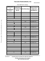
Table 1 shows the differences between the MPC7451, MPC7455, and the MPC7457 microprocessors.
Table 1. MPC7451, MPC7455, and MPC7457CPU Information
Microprocessor
Information
PVR
MPC7450/MPC7451
MPC7455
MPC7457
0x8000
0x8001
0x8002
Revision
0x0000
Name
7450
7455
Generation
4+
Exception type
Freescale Semiconductor, Inc...
7457
PPCVGER
PPCAPOLLO
L1I_size
32
L1D_size
32
L2_size
PPCAPOLLO
256
512
L2_extsize (external size)
0
L3_size
0
L3_extsize (external size)
2048
Has 8 BATs 1
0
1
number of Bats
4
8
number TLBs
128
Floating point avail 1
1
Altivec (classic) avail 1
1
Altivec (e500) avail 1
0
PCI avail 1
0
RapidIO available 1
0
PCI interface available 1
0
Ethernet interface available 1
0
Note:
1
4.2
This table is defined in dink.h as shown in Section A.1, “CPUINFO.”
A value 0 in the table indicates “no” and the value 1 indicates “yes.”
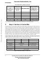
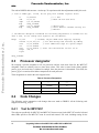
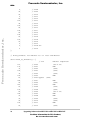
PLL Table Settings
DINK32 uses an algorithm to compute the core frequency from the processor’s bus frequency and the PLL
table information.The PMC dip switches determine the PLLBITS that can be read by software to give a
value from 0x00 to 0x1F, that is the index into this PLLTable. Thus PLLTable[PLLBITS] returns the
multiplier for determining the core frequency from the bus frequency.
For PLL encoding there is a table of 16 or 32 shorts for each PLL encoding in existence (most are relatively
common). All entries are fixed-point, scaled by 10 to avoid floating point operations; thus, 11.5 is
represented as ‘115.’ Table 2 shows the PLL settings for the MPC7451, MPC7455, and MPC7457.
4
Upgrading Software from MPC7451 to MPC7455 or MPC7457
For More Information On This Product,
Go to: www.freescale.com
Freescale Semiconductor, Inc.
CPU Information
Table 2. MPC745x PLL Settings
Multiplier for the
Core’s Frequency in
the MPC7455 V3.3 and
Later and the
MPC7457
PMC Dip Switch Setting
(Index into the PLLTable)
5
115
0x00
Multiplier value changes
0
170
0x01
New multiplier value added
75
0x02
Same multiplier value
150
0x03
Same multiplier value
70
0c04
Same multiplier value
0x05
New Multiplier Value Added
Freescale Semiconductor, Inc...
Multiplier for the
Core’s Frequency in
the
MPC7450/MPC7451
and MPC7455 V3.2
and Earlier
0
180
10
0
0x06 bypass
200
Same multiplier value
0x07
New multiplier value added
0x08
Same multiplier value
0x09
New multiplier value added
65
0c0a
Same multiplier value
130
0x0b
Same multiplier value
20
0
210
25
85
0x0c
Multiplier value changes
0
240
0x0d
New multiplier value added
0
95
0x0e
New multiplier value added
90
0x0f
Same multiplier value
30
0x10
Same multiplier value
0x11
New multiplier value added
55
0x12
Same multiplier value
110
0x13
Same multiplier value
40
0x14
Same multiplier value
100
0x15
Same multiplier value
50
0X16
Same multiplier value
120
0X17
Same multiplier value
80
0X18
Same multiplier value
140
0x19
Same multiplier value
60
0x1a
Same multiplier value
160
0x1b
Same multiplier value
0
MOTOROLA
Summary of Changes to
the Multiplier Value in the
PLLTable from the
MPC7450/MPC7451 to the
MPC7455/MPC7457
105
Upgrading Software from MPC7451 to MPC7455 or MPC7457
For More Information On This Product,
Go to: www.freescale.com
Freescale Semiconductor, Inc.
CPU Information
Freescale Semiconductor, Inc...
Table 2. MPC745x PLL Settings (continued)
Multiplier for the
Core’s Frequency in
the
MPC7450/MPC7451
and MPC7455 V3.2
and Earlier
Multiplier for the
Core’s Frequency in
the MPC7455 V3.3 and
Later and the
MPC7457
PMC Dip Switch Setting
(Index into the PLLTable)
35
135
0x1c
Multiplier value changes
0
280
0x1d
New multiplier value added
0
0
0x1e off
125
0x1f
Summary of Changes to
the Multiplier Value in the
PLLTable from the
MPC7450/MPC7451 to the
MPC7455/MPC7457
Same multiplier value
New multiplier value added
These settings are defined in pmc.c and are shown in Section A.2, “PLL Table Settings.”
5
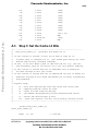
Step 3: Set the L3 Cache Bits
Each processor has a special purpose register that is used to specify cache parameters. These registers are
specific to the processor and the specific memory used for off chip cache memory. In addition to cache
memory, the off chip cache can be set up as private memory. The MPC7455 introduced two new bits in two
existing registers, the existing registers are the L3CR (SPR 1018) and the L2CR (SPR 1017). The new bits
are the L3CR[L3OH1] output hold bit and the L2CR[L3OH0] output hold bit, these bits are specific to the
MPC7455 and are reserved in all other processors. The MPC7450/MPC7451 introduced the L3ITCR0 (SPR
984) special purpose register that allows one to set the AC timings. The code and an explanation on setting
the SPR is shown in “Step 6: Setting Special Purpose Registers (SPRs).” The MPC7457 introduced the
L3ITCR1, L3ITCR2, and LCITCR3 registers, however, these settings are not changed in DINK.
L3CR[L3OH1] and the L2CR[L3OH0] bits apply only to the MPC7455. The MPC7457 has an entire
register, L3OHCR (SPR 1000) to control output AC timing. For processors other than the MPC7455, the
L3CR[L3OH1] and the L2CR[L3OH0] bits are reserved and should not change.
Register
MPC7450/MPC7451
MPC7455
MPC7457
L3CR[12]
Not implemented
New L3CR[L3OH1] bit
Not implemented
L2CR[12]
Not implemented
New L2CR[L3OH0] bit
Not implemented
L3OHCR[0-31]
Not implemented
New L3OHCR register
L3ITCR0[0-31]
Changes
Does not change
L3ITCR1[0-31]
Does not change
L3ITCR2[0-31]
Does not change
L3ITCR3[0-31]
Does not change
Figure 2. New SPRs and Bits for the MPC745x
6
Upgrading Software from MPC7451 to MPC7455 or MPC7457
For More Information On This Product,
Go to: www.freescale.com
Freescale Semiconductor, Inc.
CPU Information
All memory specific SPR settings need to be determined before the registers can be set. So the first thing
the user needs to do is look at the specifications for the memory and then determine the settings.
For example in our board, DINK32 uses the mask 0x73EF_F3C5 that is specific to our board to control
which bits are allowed to be set in the L3CR (SPR 1018), and the comments in the code indicate each
particular bit setting that is set in DINK32. The function in DINK32 does all this in the
cache_inval_enable_L3 function that is shown below.
Freescale Semiconductor, Inc...
Code snippets illustrating the specific code for the MPC7450/MPC7451, MPC7455, and MPC7457 from
the cache_inval_enable_L3 function are shown here. The entire function is shown in Appendix A,
“Complete Code Examples,” that includes specific code for dealing with the MPC7457 Chip Errata 20 and
21. Note that the code text in italics is new for the MPC7457.
//----------------------------------------------------------------------// cache_inval_enable_L3 - Invalidate and enable the L3
.global cache_inval_enable_L3
cache_inval_enable_L3:
mfspr
rlwinm
cmpli
beq
cmpli
beq
cmpli
beq
xor
b
r9, 287
// read PVR
r9,r9,16,16,31 // shift down 16 bits
0,0,r9,0x8000
// Vger pvr
cache_inval_enable_L3_MPC7450
0,0,r9,0x8001
// Apollo pvr
cache_inval_enable_L3_MPC7450
0,0,r9,0x8002
// Apollo7 pvr MPC7457
cache_inval_enable_L3_MPC7450
r3,r3,r3// All others: There is no L3 to enable.
cache_inval_enable_L3_exit// just return zero
........
#endif
//
Do not allow user to set L3CR[L3E/0]; we'll do that below.
lis
r4,0x73ef
//
//
//
//
//
//
//
//
//
MOTOROLA
L3E/0
L3PE/1
L3APE/2
L3SIZ/3
L3CLKEN/4
L3CR/5
L3CLK[6:8]
=
=
=
=
=
0
x
x
x
0
(don't allow enabling yet)
(parity)
(address parity)
(0 - 1MB; 1 - 2MB)
(L3 clock enable -
see MPC7450_errata20)
= 0
(Must be set by software named L3DX?)
= xxx (L3 divider)
Upgrading Software from MPC7451 to MPC7455 or MPC7457
For More Information On This Product,
Go to: www.freescale.com
Freescale Semiconductor, Inc.
CPU Information
//
//
//
//
//
//
IONLY/9
L3CR[10]
L3CR[11]
L3CR[12]
L3SPO/13
L3CKSP[14:15]
=
=
=
=
=
=
x
x
0
x
x
xx
(Instructions only)
(Extended L3CLK on MPC7457)
(reserved)MPC7457 L3CKSPEXT
(L3OH1)MPC7455 only
(sample point overide)
(clock sample point)
Freescale Semiconductor, Inc...
cmpli
0,0,r9,0x8002
// Apollo7 pvr
beq
MPC7457_L3CR_mask
//need different mask for non-7457 parts
ori
r4,r4,0xf3c5
//bit 30 is reserved for non-7457
b
no_MPC7457_L3CR_mask
MPC7457_L3CR_mask:
ori
r4,r4,0xf3c7
no_MPC7457_L3CR_mask:
and
oris
//
// L3PSP[16:18]
= xxx (processor sample point)
// L3REP/19
= x
(Replacement algorithm - 0 default)
// L3HWF/20
= 0
(L3 Hardware Flush - not here)
// L3I/21
= 0
(global invalidate - not set here)
// L3RT[22:23]
= xx (SRAM type - MSUG2 DDR SRAMs)
// L3CYA/24
= x
(L3 SRAM clock control bit)
// DONLY/25
= x
(data only)
// L3CR[26:28]
= 000 (reserved)
// PMEN/29
= x
(Private memory enable)
// L3CR/30
= 0
(reserved on non-MPC7457)
// PMSIZ/30
= x
(L3PM 4MB on MPC7457)
// PMSIZ/31
= x
(0 - 1MB; 1 - 2MB)
r4,r3,r4// Mask off non-user bits, preserve r3
r4,r4,0x0400// Enforce L3DX/5 in L3CR pattern (not optional)
dssall
// Cancel any pending data stream operations with dssall
.long 0x7e00066c // Not all assemblers generate
// the dssall instruction yet
sync
// Finish any pending store ops in LSU (UM p3-65)
.........
// Look at SRAM type; if PB2, do not play with L3ITCR0 register below.
See “Step 6: Setting Special Purpose Registers (SPRs)” for the L3ITCR0 description and code.
8
Upgrading Software from MPC7451 to MPC7455 or MPC7457
For More Information On This Product,
Go to: www.freescale.com
Freescale Semiconductor, Inc.
Step 4: Setup and Perform Software Flush
6
Modify Code to Test for the MPC7457 Case
All these steps are the same for the MPC7451, MPC7455, and MPC7457. DINK32 has separate tests for
each processor, so if your code has detection software for various processors, you will also need to add
processor tests (detection) for the MPC7457. If your code is limited to only a single MPC745x processor, it
is not necessary to add these tests.
6.1
Step 4: Setup and Perform Software Flush
Freescale Semiconductor, Inc...
The MPC7451, MPC7455, and MPC7457 do not support an L1 hardware flush, thus a software flush
algorithm must be used. This has not changed from the MPC7450/MPC7451 to the MPC7455/MPC7457.
However, it is necessary to detect the MPC7457 and perform a software flush. Text in italics is new code for
the MPC7457.
The following code fragment from cache.S shows how DINK32 determines the type of processor flash and
performs the correct flushing mechanism.
// Which part are we dealing with?
mfspr
r9,287
//Only use upper half of PVR
//Be careful! srawi r9,r9,16 will sign extend the MPC7450 and MPC7455
rlwinm r9,r9,16,16,31
//Be careful! cmpi r9,0x8nnn will sign extend and not be equal on 7450/7455
cmpli
0,0,r9,0x0008
//Is this MPC750/MPC755?
beq
HW_flush_750_DCache //Yes? Use HW flush assist.
cmpli
0,0,r9,0x000c
//Is this MPC7400?
beq
HW_flush_7400_DCache
//Do hardware assisted flush
cmpli
0,0,r9,0x800C
//Is this MPC7410?
beq
HW_flush_7400_DCache
//Do hardware assisted flush
cmpli
0,0,r9,0x8000
//Is this MPC7450?
beq
SW_flush_7450_DCache
//Do software flush
cmpli
0,0,r9,0x8001
//Is this MPC7455?
beq
SW_flush_7450_DCache
//Do software flush
cmpli
0,0,r9,0x8002
//Is this MPC7457?
beq
SW_flush_7450_DCache
//Do software flush
6.2
Setting the HID0 Register Appropriately
The HID0 (SPR 1008) register defines the L1 cache characteristics, time base, branch table, and many other
characteristics of each processor. The MPC7450 RISC Microprocessor Family User’s Manual describes
these bits in detail. In all processors other than the MPC745x, HID0[0] was used to enable the MCP and this
feature has since been moved to HID1[0]. In the MPC745x, HID0[0] is reserved and is hard coded to 1, and
the user must not change this bit. Simply, the MPC7450 RISC Microprocessor Family User’s Manual
indicates that bits HID0[0–4] = ‘0b1000_0’. This was true for the MPC7451. To support the MPC7457 in
DINK32 we need to add a similar test to maintain this bit in the same manner as for the MPC7451.
HID0 is set up initially in except2.S, however, when the L1 cache is enabled and/or disabled, the cache
routines need to turn on/off the bits associated with L1 cache, HID0[16-21]. In addition, the code must
ensure that HID0[0] is not changed.
MOTOROLA
Upgrading Software from MPC7451 to MPC7455 or MPC7457
For More Information On This Product,
Go to: www.freescale.com
Freescale Semiconductor, Inc.
Step 4: Setup and Perform Software Flush
The MPC7451 preferred bit setting for HID0 is 0x0410C0BC.
The MPC7455 and MPC7457 HID0 preferred bit setting is 0x0410c1bc and is defined in DINK32, config.h
as:
#define DEFAULT_HID0_7457 0x0410C1BC
Freescale Semiconductor, Inc...
As shown in the table below the only bit that is different is HID0[23], the XBSEN bit, which is the Extended
BAT Block Size Enable allowing BAT block sizes up to 4 Gigabytes.
Processor
HID0 bit settings
MPC7451
0x0410C0BC
MPC7455
0x0410C1BC
MPC7457
0x0410C1BC
Figure 3. HID0 bit settings
This code snippet in cache.S performs a test for the MPC7451/MPC7455/MPC7457 and does not set the bit
HID0[0]. The complete code is in Appendix A, “Complete Code Examples”. Text in italics in the code is
new for the MPC7457.
.global cache_inval_enable_L1
cache_inval_enable_L1:
mfspr
r8,1008
// Get current HID0=1008
// If this is MPC7450 ignore HID0/0 in following comparison. It will always
// read as a one.
mfspr
r9,287
//Only use upper half of PVR
rlwinm r9,r9,16,16,31 //Shift down 16 bits
cmpli
0,0,r9,0x8000
// MPC7450 pvr
beq
ignore_HID0_0
cmpli
0,0,r9,0x8001
// MPC7455 pvr
beq
ignore_HID0_0
cmpli
0,0,r9,0x8002
// MPC7457 pvr
beq
ignore_HID0_0
b
compare_desired_w_current
ignore_HID0_0:
rlwinm r8,r8,0,1,31
compare_desired_w_current:
The code then continues setting up HID0.
6.3
Various Settings at Initialization
Initialization settings have not changed from the MPC7450/MPC7451 to the MPC7455 and MPC7457.
However, since each processor is detected individually, it is necessary to add the code to detect the
MPC7457 and perform the same functions as for the other MPC745x processors.
During initialization DINK32 will determine the processor from the PVR and then perform initialization of
specific SPRs, memory, and other attributes of the processor and the board environments. Most of this
10
Upgrading Software from MPC7451 to MPC7455 or MPC7457
For More Information On This Product,
Go to: www.freescale.com
Freescale Semiconductor, Inc.
Set the BATs for the MPC7455 and MPC7457
initialization is done in except2.S. The specific settings for the MPC7455/MPC7457 are set in except2.S as
shown below.
Freescale Semiconductor, Inc...
Enable Altivec, set MPC7450/MPC7451 modes, initialize HID0 with the default from config.h,
initialize L2, set MPC7450/MPC7451 Java mode, and set the BATs for the MPC7455. All these
actions were true for the MPC7451 as well, we just added code to ensure the same actions for the
MPC7455 and MPC7457. The code snippets below show the additional code detecting the
MPC7457 (PVR 0x8002).
NOTE
In most cases, the code will compare this processor’s PVR to known PVRs
and perform actions associated with the correct processor. This code
compares the PVR, then branch on equal to the function to perform the
activity. However, the added tests for MPC7457 will branch not equal
around the same MPC7451/55 functions. Thus, in effect, performing the
same MPC7451/55 functions, that is bne versus beq.
Only the code snippet for enabling AltiVec is shown here. All the other code is similar and the complete
code is in Appendix A, “Complete Code Examples.”
1. Enable Altivec
// For MPC7xxx parts, enable AltiVec so we
// contents.
cmpli
0,0,r20,0x000C
// MPC7400
beq
enable_altivec
cmpli
0,0,r20,0x8000
//
beq
enable_altivec
cmpli
0,0,r20,0x8001
//
beq
enable_altivec
cmpli
0,0,r20,0x8002
//
beq
enable_altivec
cmpli
0,0,r20,0x800C
//
bne
no_enable_altivec
2.
3.
4.
5.
can save/restore the
MPC7450
MPC745x
MPC7457
MPC7410
Do set v’ger modes
Initialize HID0 with the default from config.h
Do initialize L2 (This is not required, the L2 can be initialized at any point in the code)
Do set v’ger Java mode
7
Step 5: Block Address Translation Registers
(BATs) for the MPC7455 and MPC7457
The MPC7451 has four pairs of IBATs and DBATs. The MPC7455 and MPC7457 has eight pairs of IBATs
and DBATs. The code snippets below shows a method to set the four extra pairs of IBATs and DBATs.
7.1
Set the BATs for the MPC7455 and MPC7457
This code snippet shows the additional 4 IBATs and DBATs. Code in italics is specific to the MPC7457
MOTOROLA
Upgrading Software from MPC7451 to MPC7455 or MPC7457
For More Information On This Product,
Go to: www.freescale.com
Freescale Semiconductor, Inc.
Set the BATs for the MPC7455 and MPC7457
ldb_standard:
cmplwi
beq
cmplwi
beq
lis
ori
b
ldb_extended:
lis
ori
b
r20,0x8001
ldb_extended
r20,0x8002
ldb_extended
r5,BATS_standard@h
r5,r5,BATS_standard@l
load_bat_array
// MPC7455
r5,BATS_apollo@h
r5,r5,BATS_apollo@l
load_bat_array
// Extended BATs
// MPC7457
// Standard BATs
Freescale Semiconductor, Inc...
// Extended BATS (Apollo)
BATS_apollo:
// Flash space + EUMBBAR
.long
.long
.long
.long
b_BEPI(
b_BPRN(
b_BEPI(
b_BPRN(
0xFC000000
0xFC000000
0xFC000000
0xFC000000
)
)
)
)
+
+
+
+
b_64M
+ b_VS
b_WIMG(0,0,0,0)
b_64M
+ b_VS
b_WIMG(0,1,0,0)
+
+
+
+
b_VP
b_RW
b_VP
b_RW
// IBAT0
0x00000000
0x00000000
0x00000000
0x00000000
)
)
)
)
+
+
+
+
b_1G
+ b_VS
b_WIMG(0,0,0,0)
b_1G
+ b_VS
b_WIMG(0,0,0,0)
+
+
+
+
b_VP
b_RW
b_VP
b_RW
// IBAT1
// DBAT0
// SDRAM space
.long
.long
.long
.long
b_BEPI(
b_BPRN(
b_BEPI(
b_BPRN(
// DBAT1
// PCI memory space
.long
.long
.long
.long
b_BEPI(
b_BPRN(
b_BEPI(
b_BPRN(
0x80000000
0x80000000
0x80000000
0x80000000
)
)
)
)
+
+
+
+
b_512M
+ b_VS
b_WIMG(0,1,0,0)
b_512M
+ b_VS
b_WIMG(0,1,0,1)
+
+
+
+
b_VP
b_RW
b_VP
b_RW
// IBAT2
.long
.long
.long
.long
b_BEPI(
b_BPRN(
b_BEPI(
b_BPRN(
0x78000000
0x78000000
0x78000000
0x78000000
)
)
)
)
+
+
+
+
b_128M
+ b_VS
b_WIMG(0,0,0,0)
b_128M
+ b_VS
b_WIMG(0,1,0,0)
+
+
+
+
b_VP
b_RW
b_VP
b_RW
// IBAT3
// DBAT2
// DBAT3
8
Step 6: Setting Special Purpose Registers
(SPRs)
The following section provides a general discussion on how SPRs are set. For further details on setting SPRs
see the MPC7450 RISC Microprocessor Family User’s Manual.
12
Upgrading Software from MPC7451 to MPC7455 or MPC7457
For More Information On This Product,
Go to: www.freescale.com
Freescale Semiconductor, Inc.
SPRs
8.1
SPRs
All the SPRs specific to the MPC7451, MPC7455, and MPC7457 must be saved and restored. Code
performing the save and restore must be aware of the additional SPRs introduced by these processors.
8.2
Setting the SPRs
Freescale Semiconductor, Inc...
As discussed previously, in order to use the L3 cache, the special purpose register L3ITCR0 (SPR 984) must
receive special attention. The MPC7451, MPC7455, and MPC7457 determines its own settings for the
L3ITCR0 during hardware startup. It is recommended that the default settings for the L3ITCR0 are used for
the MPC7457.
For the MPC7455, the setting can be adjusted as shown below to increase system margin. The MPC7455
L3ITCR0 register causes the L3 input clock phases to be shifted in a way similar, but not identical, to the
way L2CR[L3OH0] and L3CR[(L3OH1]) registers work for the output timings on the MPC7455. The
operation of this register is rather complex and improper settings can cause erratic behavior on the L3 and
is only applicable for DDR.
Dink adjusts the setting for MPC7451 and MPC7455 class parts in cache.S by manipulating the L3ITCR0
register, as illustrated below.
NOTE:
This information for the L3ITCR0 special purpose registers is only
applicable to the MPC7455. Do not make these changes for the MPC7457.
The L3ITCR0 value (SPR 984) adds/subtracts some extra taps to the clock DLL beyond what it determined
via its own feedback mechanism. In actuality, each sequential “1” bit in bits 0-22 indicates an internal
delay to align the clock edge to the center of the data. The algorithm implements via a bit setting specific
number of taps. According to the design team this table shows the association of settings to frequency.
Table 3. Frequency versus Adjustment Value for the MPC7451 and MPC7457
Frequency
Additional Taps
175
+4
200
+3
250
+1
These values hold for both the MPC7451 and the MPC7457.
The frequency values shown are the SRAM frequencies (for example, 175 = 350Mt/s DDR). Mt/s is mega
transfers per second.
One can extrapolate the above table for frequencies not shown.
NOTE
Always read the register L3ITCR0 first, then shift bits into it, shift in 1s if
shifting right, 0s if shifting left. DINK32 uses the rlwinm instruction for
this. Also, one must set L3ITCR0[24] to force the processor to use the
shifted value. See the code example below.
MOTOROLA
Upgrading Software from MPC7451 to MPC7455 or MPC7457
For More Information On This Product,
Go to: www.freescale.com
Freescale Semiconductor, Inc.
SPRs
The code in DINK32 adds an extra +4 to the tap. To experiment with other adjustments modify this code.
// Look at SRAM type; if PB2, do not play with L3ITCR0 register below.
li
and
cmpi
beq
cmpli
beq
r5,0x0300
r5,r3,r5
0,0,r5,0x0300
skip_L3ITCR0
0,0,r9,0x8002
skip_L3ITCR0
// 3 = PB2
// Mask off non-user bits
// Apollo7 pvr
// Leave default L3ITCR0 setting for
// MPC7457
Freescale Semiconductor, Inc...
// The MPC7457 designers recommend the following adjustments to L3ITCR0 for the
7450 & 7455, no not change this register for the MPC7457.
mfspr
r5,984
rlwinm
oris
ori
xori
mtspr
isync
// L3ITCR0: adjust SRAM Clock edges by shifting
r5,r5,28,4,31
// for data being read from bus by adding
r5,r5,0xf000
// four additional taps on a pulse shaper
r5,r5,0x00ff
r5,r5,0x007f // these two instructions set bit 24 on
984,r5
skip_L3ITCR0:
8.3
Processor designator
We assigned a specific designator to all our processors and the code must check for the MPC7457
designator. These are arbitrary since we chose these values. This value is stored in the global variable
process_type, and each value is #defined in config.h. Once the processor is determined via its PVR, the
process_type is set and used for further comparisons for each processor.
These designators are used in the code snippets below.
Table 4. Processor Designators
8.4
Processor
config.h name
process_type value
MPC7451
PPCVGER
38
MPC7455
PPCAPOLLO
3b
MPC7457
PPCAPOLLO7
3d
Code Changes
The following section summarizes code changes that were made to DINK32. All the following code
snippets are from reg_swap.S.
8.4.1
Test for MPC7457
The code tests specifically for MPC7451 and MPC7455, thus new tests for the MPC7457 must be built and
those SPRs specific to the MPC7457 must be saved and restored. Full code, including testing for the
14
Upgrading Software from MPC7451 to MPC7455 or MPC7457
For More Information On This Product,
Go to: www.freescale.com
Freescale Semiconductor, Inc.
SPRs
MPC7451 and MPC7455, is shown in Appendix A, “Complete Code Examples. The following is a code
snippet of how the code changes for the MPC7457.
Save MPC7457 specific SPRs.
Freescale Semiconductor, Inc...
//
check for the MPC7457
lis
r4,process_type@h
ori
r4,r4,process_type@l
lbz
r4,0(r4)
cmpi
0,0,r4,PPCAPOLLO7 // PPCAPOLLO7 MPC7457 from config.h
bne
cr0,noMPC7457
// save MPC7457 special purpose registers.
mfspr
r4,l3ohcr
// L3OHCR= 1000
stw
r4,L3OHCR_LOC*spr_inc(r3)
mfspr
r4,l3itcr0
// L3ITCR0= 984
stw
r4,L3ITCR0_LOC*spr_inc(r3)
mfspr
stw
mfspr
stw
mfspr
stw
r4,l3itcr1
r4,L3ITCR1_LOC*spr_inc(r3)
r4,l3itcr2
r4,L3ITCR2_LOC*spr_inc(r3)
r4,l3itcr3
r4,L3ITCR3_LOC*spr_inc(r3)
// L3ITCR1= 1001
// L3ITCR2= 1002
// L3ITCR3= 1003
noMPC7457:
.....
Restore MPC7457 specific SPRs
// check for the MPC7457
lis
r4,process_type@h
ori
r4,r4,process_type@l
lbz
r4,0(r4)
cmpi
0,0,r4,PPCAPOLLO7 // PPCAPOLLO7 MPC7457 from config.h
bne
cr0,noStoreMPC7457
// save MPC7457 special purpose registers.
lwz
r4,L3OHCR_LOC*spr_inc(r3)
mtspr
l3ohcr,r4
// L3OHCR= 1000
lwz
r4,L3ITCR0_LOC*spr_inc(r3)
mtspr
l3itcr0,r4
// L3ITCR0= 984
lwz
r4,L3ITCR1_LOC*spr_inc(r3)
mtspr
l3itcr1,r4
// L3ITCR1= 1001
lwz
mtspr
lwz
mtspr
noStoreMPC7457:
MOTOROLA
r4,L3ITCR2_LOC*spr_inc(r3)
l3itcr2,r4
r4,L3ITCR3_LOC*spr_inc(r3)
l3itcr3,r4
// L3ITCR2= 1002
// L3ITCR3= 1003
Upgrading Software from MPC7451 to MPC7455 or MPC7457
For More Information On This Product,
Go to: www.freescale.com
Freescale Semiconductor, Inc.
SPRs
8.4.2
Checking for Processor Specific Designator
This code determines via the special designator if we have a MPC7451/MPC7455/MPC7457 mode
processor and, if not, then we ignore all the settings. It is required for saving registers and restoring registers.
r4,process_type@h
ori
r4,r4,process_type@l
lbz
r4,0(r4)
... other code
set_vger:
Freescale Semiconductor, Inc...
lis
cmpi
beq
cmpi
beq
0,0,r6,0x38
set_vger_apollo
0,0,r6,0x3B
set_vger_apollo
cmpi
bne
0,0,r6,0x3D
end_setting
......
set_vger_regs:
cmpi
beq
cmpi
beq
cmpi
bne
9
0,0,r6,0x38
set_vger_apollo_regs
0,0,r6,0x3B
set_vger_apollo
0,0,r6,0x3D
end_set_regs
Conclusion
Armed with this information, you can either modify DINK32 or your own code to accommodate for the
MPC7455 or the MPC7457 processor.
There are several pieces of code that need to be added to MPC7450/MPC7451 and MPC7455 aware code
to also manage the MPC7457. One needs to add code to understand the MPC7457 PVR (0x8002), add the
PLL setting values and CPU information, set the L3 cache bits, set the HID0[XBSEN/23] bit if desired (it
is not required), recognize that HID0[0] bit is reserved, enable various features of the MPC7457, and set bits
in the L2CR, L3CR, and L3ITCR0.
10
Revision History
Table 5 lists the revisions to this document.
16
Upgrading Software from MPC7451 to MPC7455 or MPC7457
For More Information On This Product,
Go to: www.freescale.com
Freescale Semiconductor, Inc.
SPRs
Table 5. Revision History
Revision
Number
Changes
Initial release
0.1
Nontechnical reformatting
Freescale Semiconductor, Inc...
0.0
MOTOROLA
Upgrading Software from MPC7451 to MPC7455 or MPC7457
For More Information On This Product,
Go to: www.freescale.com
Freescale Semiconductor, Inc.
SPRs
Appendix A Complete Code Examples
Freescale Semiconductor, Inc...
A.1
CPUINFO
//--------------------------------------------------------------------------//
CPUInfo -- a database of CPU information
//--------------------------------------------------------------------------typedef struct st_cpuinfo {
USHORT pvr;
// Upper PVR
USHORT rev_min;
// REV part of PVR must be >=
this to qualify.
char
Name[ 10 ];
// Official name
char
NickName[ 12 ];
// Nickname
char
Gen[4];
// Generation.
char
type;
// exception handler type
USHORT L1I_size;
// in K.
USHORT
USHORT
USHORT
USHORT
USHORT
char
USHORT
USHORT
char
char
char
char
char
char
char
} CPUINFO;
L1D_size;
L2_size;
L2_extsize;
L3_size;
L3_extsize;
HasXBSEN;
no_BATs;
no_TLBs;
HasFP;
HasAV;
HasAVe;
PCI;
HasRapidIO;
HasPCI;
HasENet;
//
//
//
//
//
//
//
//
//
//
//
//
//
//
//
in K.
in K.
in K.
in K.
in K.
Has larger BAT size support
I+D
# of TLBs
Has floating point
Has AltiVec (classic)
Has AltiVec (e500)
Has PCI interface
Has RapidIO interface
Has PCI interface
Has Ethernet interface(s)
6. The setting for the 7450/55/57 is initilaized in main.c as:
//--------------------------------------------------------------------------//
cdb -- various collected data on this CPU.
//--------------------------------------------------------------------------CPUINFO cdb[] = {
// PVR
REV
NAME
NICKNAME
GEN
// L1I L1D L2
L2X L3
L3X
XBSEN
// #BATS #TLBS FP AV AVe PCI RIO ENET
CLASS
// MPC7451
18
Upgrading Software from MPC7451 to MPC7455 or MPC7457
For More Information On This Product,
Go to: www.freescale.com
Freescale Semiconductor, Inc.
SPRs
{ 0x8000, 0x0000, "7450",
"V'ger",
32, 32, 256,
0, 0, 2048, 0,
4,
128,
1, 1, 0, 0, 0, 0 },
Freescale Semiconductor, Inc...
// MPC7455
{ 0x8001, 0x0000, "7455",
"Apollo",
32, 32, 256,
0, 0, 2048, 1,
8,
128,
1, 1, 0, 0, 0, 0 },
// MPC7457
{ 0x8002, 0x0000, "7457",
"Apollo7",
32, 32, 512,
0, 0, 2048, 1,
8,
128,
1, 1, 0, 0, 0, 0 },
A.2
"4+",
PPCVGER,
"4+",
PPCAPOLLO,
"4+",
PPCAPOLLO,
PLL Table Settings
The M7455_V3_PLLTable is used for the MPC7457 as well.
//--------------------------------------------------------------------------// PLL Encoding. There is a table of 16 or 32 shorts for each pll
// encoding in existence (most are relatively common).
//
// All entries are fixed-point, scaled by 10 to avoid floating
// point operations; thus, 6.5X is represented as "65".
// M745X_PLLTable: For MPC7451, MPC7451, MPC7455 <= 2.x
// M745X_PLLTable: For MPC7451, MPC7451, MPC7455 <= 2.x
short M745X_PLLTable[] = { // MPC7451 and MPC7455 V3.2 and earlier
// PLL
5,
// 0x00
0,
// 0x01
75,
// 0x02
150,
// 0x03
70,
// 0x04
0,
// 0x05
10,
// 0x06 bypass
0,
// 0x07
20,
// 0x08
0,
// 0x09
65,
130,
25,
0,
MOTOROLA
//
//
//
//
0x0A
0x0B
0x0C
0x0D
Upgrading Software from MPC7451 to MPC7455 or MPC7457
For More Information On This Product,
Go to: www.freescale.com
Freescale Semiconductor, Inc.
Freescale Semiconductor, Inc...
SPRs
0,
90,
30,
0,
55,
110,
40,
100,
50,
120,
80,
140,
60,
160,
35,
0,
0,
0
//
//
//
//
//
//
//
//
//
//
//
//
//
//
//
0x0E
0x0F
0x10
0x11
0x12
0x13
0x14
0x15
0x16
0x17
0x18
0x19
0x1A
0x1B
0x1C
// 0x1D
// 0x1E off
// 0x1F
};
// M7455_PLLTable: For MPC7455 V3.3 or later and MPC7457
short M7455_V3_PLLTable[] = {
// PLL
20
115,
170,
75,
150,
70,
180,
10,
200,
20,
210,
65,
130,
85,
240,
//
//
//
//
//
//
//
//
//
//
//
//
//
//
0x00
0x01
0x02
0x03
0x04
0x05
0x06 bypass
0x07
0x08
0x09
0x0A
0x0B
0x0C
0x0D
95,
90,
30,
105,
55,
//
//
//
//
//
0x0E
0x0F
0x10
0x11
0x12
MPC7451 comparison
(was 0.5x)
NEW
(same)
(same)
(same)
NEW
(same)
NEW
(same)
NEW
(same)
(same)
(was 2.5x)
NEW
NEW
(same)
(same)
NEW
(same)
Upgrading Software from MPC7451 to MPC7455 or MPC7457
For More Information On This Product,
Go to: www.freescale.com
Freescale Semiconductor, Inc.
Freescale Semiconductor, Inc...
SPRs
110,
40,
100,
50,
120,
80,
140,
60,
160,
135,
280,
0,
125
A.3
//
//
//
//
//
//
//
//
//
//
//
//
//
0x13
0x14
0x15
0x16
0x17
0x18
0x19
0x1A
0x1B
0x1C
0x1D
0x1E off
0x1F
(same)
(same)
(same)
(same)
(same)
(same)
(same)
(same)
(same)
(was 3.5x)
NEW
(same)
NEW
Step 3: Set the Cache L3 Bits
//----------------------------------------------------------------------// cache_inval_enable_L3 - Invalidate and enable the L3
//
// If this routine is entered, we will use as much of arg0 (in r3)
//
as makes sense to configure the L3. User should pass exactly the final
//
desired L3CR setting, including L3CR[L3E].
// In fact, if the user doesn't pass in L3CR with L3E set (e.g, like the
//
user mistakenly gives us all zeroes) let's just exit without enabling.
// If this routine is entered with the L3 enabledthe user is asking for
//
the same settings we will just return.
// If this routine is entered with the L3 enabled and the user is asking for
//
different settings we will flush and disable the L3 before invalidating
//
and reenabling.
//
// Register usage:
//
r3 - enter with desired L3CR value and return with actual L3CR
//
r4 - temporary mask(ed) values for L3CR
//
r5 - target for L3CR reads for polling
//
r6 - save MSSCR0 during MPC7451_errata21 workaround and restore
//
r9 - current PVR shifted right 16 bits
//
r12 - saved link register (r12 will not be used by routines called)
//----------------------------------------------------------------------.global cache_inval_enable_L3
cache_inval_enable_L3:
mfspr
MOTOROLA
r9, 287
// read PVR
Upgrading Software from MPC7451 to MPC7455 or MPC7457
For More Information On This Product,
Go to: www.freescale.com
Freescale Semiconductor, Inc.
SPRs
Freescale Semiconductor, Inc...
rlwinm
cmpli
beq
cmpli
beq
cmpli
beq
xor
b
r9,r9,16,16,31 // shift down 16 bits
0,0,r9,0x8000
// Vger pvr
cache_inval_enable_L3_MPC7450
0,0,r9,0x8001
// Apollo pvr
cache_inval_enable_L3_MPC7450
0,0,r9,0x8002
// Apollo7 pvr
cache_inval_enable_L3_MPC7450
r3,r3,r3// All others: There is no L3 to enable.
cache_inval_enable_L3_exit// just return zero
// Cache initialization, invalidation, and enabling for MPC7450, and 7455
cache_inval_enable_L3_MPC7450:
// Check that L3 is not enabled already with User's
// desired value; return if it is
mfspr
r5,1018
// Get L3CR
cmpw
r3,r5
// Is L3 already configured as user desires?
beq
cache_inval_enable_L3_exit// Yes, exit without changes
// Check if L3 was already enabled with other values and needs flushing.
andis. r4,r5,0x8000// Is L3E/0 already set?
beq
check_L3E_MPC7450// No (result = 0), continue configuring
mflr
r12
// Yes, save link register
bl
cache_flush_disable_L3// Flush and disable
mtlr
r12
// Restore link register
mfspr
r5,1018
// Refresh r5 with L3CR
check_L3E_MPC7450:
// Allow init of L3CR without the L3E bit set. This allows initializing
// the L3 interface while using the entire space for Private Memory.
// tpeters - 111602
// Don't enable if user didn't set L3E
//
andis. r4,r3,0x8000
// Did the user ask to set L3E?
//
bne
init_L3_Cache_MPC7450// Yes (result !=0), then go initialize.
//
mr
r3,r5
// No, return the current value of L3CR
//
b
cache_inval_enable_L3_exit// and exit without changes
init_L3_Cache_MPC7450:
#define MPC7450_errata21 //This is supposed to be perf impact only
#ifdef MPC7450_errata21 // D fetches may allocate in IONLY L3 or
mfspr
lis
ori
and.
22
// I fetches may allocate in DONLY L3
r6,1014
// Save current value of MSSCR0 = spr 1014
r4,0x0040// IONLY/9
r4,r4,0x0040// DONLY/25
r4,r3,r4// Are we doing an IONLY or DONLY init
Upgrading Software from MPC7451 to MPC7455 or MPC7457
For More Information On This Product,
Go to: www.freescale.com
Freescale Semiconductor, Inc.
SPRs
beq
init_L3_wo_errata21 // No, then MPC7450_errata21 doesn't apply
ori
r4,r6,0x0003
xori
r4,r4,0x0003// Turn off HW prefetching MSSCR0[30:31]
sync
mtspr
1014,r4
init_L3_wo_errata21:
#endif
//
Do not allow user to set L3CR[L3E/0]; we'll do that below.
Freescale Semiconductor, Inc...
lis
r4,0x73ef
//
//
L3E/0
L3PE/1
= 0
= x
//
//
//
//
//
//
//
//
//
//
//
//
//
L3APE/2
L3SIZ/3
L3CLKEN/4
= x
= x
= 0
L3CR/5
L3CLK[6:8]
IONLY/9
L3CR[10]
L3CR[11]
L3CR[12]
L3SPO/13
L3CKSP[14:15]
(don't allow enabling yet)
(parity)
(address parity)
(0 - 1MB; 1 - 2MB)
(L3 clock enable see MPC7450_errata20)
= 0
(Must be set by software named L3DX?)
= xxx (L3 divider)
= x
(Instructions only)
= x
(Extended L3CLK on MPC7457)
= 0
(reserved)MPC7457 L3CKSPEXT
= x
(L3OH1)MPC7455 only
= x
(sample point overide)
= xx (clock sample point)
cmpli
0,0,r9,0x8002
// Apollo7 pvr
beq
MPC7457_L3CR_mask
//need different mask for non-7457 parts
ori
r4,r4,0xf3c5
//bit 30 is reserved for non-7457
b
no_MPC7457_L3CR_mask
MPC7457_L3CR_mask:
ori
r4,r4,0xf3c7
no_MPC7457_L3CR_mask:
//
//
//
//
//
MOTOROLA
L3PSP[16:18]
L3REP/19
L3HWF/20
L3I/21
L3RT[22:23]
=
=
=
=
=
xxx
x
0
0
xx
(processor sample point)
(Replacement algorithm - 0 default)
(L3 Hardware Flush - not here)
(global invalidate - not set here)
(SRAM type - MSUG2 DDR SRAMs)
Upgrading Software from MPC7451 to MPC7455 or MPC7457
For More Information On This Product,
Go to: www.freescale.com
Freescale Semiconductor, Inc.
SPRs
and
oris
Freescale Semiconductor, Inc...
//
// L3CYA/24
= x
(L3 SRAM clock control bit)
// DONLY/25
= x
(data only)
// L3CR[26:28]
= 000 (reserved)
// PMEN/29
= x
(Private memory enable)
// L3CR/30
= 0
(reserved on non-MPC7457)
// PMSIZ/30
= x
(L3PM 4MB on MPC7457)
// PMSIZ/31
= x
(0 - 1MB; 1 - 2MB)
r4,r3,r4// Mask off non-user bits, preserve r3
r4,r4,0x0400// Enforce L3DX/5 in L3CR pattern (not optional)
dssall
// Cancel any pending data stream operations with dssall
.long 0x7e00066c // Not all assemblers generate
// the dssall instruction yet
sync
// Finish any pending store ops in LSU (UM p3-65)
#define MPC7450_errata20
#ifdef MPC7450_errata20
// Set all L3CR bits to their desired values except L3CLKEN, L3E, L3PE, and L3I
//
lis
r5,0xbffff//this mask is incorrect - tpeters 111602
//
ori
r5,r5,0xffff
//
andis. r4,r3,0xbfff
lis
r5,0x37ff//correct mask to make sure L3CLKEN, L3E
ori
r5,r5,0xfbff//L3PE, and L3I are not enabled - tpeters
and
r4,r4,r5//Set all L3CR bits to their
//desired values except
mtspr
1018,r4
//L3CLKEN, L3E, L3PE, and L3I
#endif
oris
r4,r4,0x0800// Set L3CR[L3CLKEN/4]
mtspr
1018,r4
li
r5,128
// Wait for minimum 100 processor clocks
inval_L3_MPC7450_wait:// after changing L3CLKEN
addi
r5,r5,-1
cmpi
0,0,r5,0// Same as cmpwi r5,0 CHECK ELSEWHERE
bne
inval_L3_MPC7450_wait// Perform a delay loop
ori
r4,r4,0x0400// Set L3CR[L3I/21] to start invalidate routine
mtspr
1018,r4
inval_L3_MPC7450_poll:
mfspr
mtcrf
bc
24
r5,1018
0xff,r5
// poll for invalidate to complete, L3CR[L3I/21] = 0
0xC,21,inval_L3_MPC7450_poll
Upgrading Software from MPC7451 to MPC7455 or MPC7457
For More Information On This Product,
Go to: www.freescale.com
Freescale Semiconductor, Inc.
SPRs
// Look at SRAM type; if PB2, do not play with L3ITCR0 register below.
// Same for late-write SRAM don’t change the L3ITCR0
Freescale Semiconductor, Inc...
li
and
cmpi
beq
cmpli
beq
r5,0x0300
r5,r3,r5
0,0,r5,0x0300
skip_L3ITCR0
0,0,r9,0x8002
skip_L3ITCR0
// 3 = PB2
// Mask off non-user bits
// Apollo7 pvr
// Leave default L3ITCR0 setting for
// MPC7457
// Somerset recommends the following adjustments to L3ITCR0 for the 7450 & 7455
// for Samsumg 4Mb DDR.
mfspr
r5,984
// L3ITCR0: Supposed to adjust SRAM Clock edges
rlwinm
oris
ori
xori
mtspr
isync
r5,r5,28,4,31// for data being read from bus by adding
r5,r5,0xf000// four additional taps on a pulse shaper
r5,r5,0x00ff
r5,r5,0x007f
984,r5
skip_L3ITCR0:
#ifdef MPC7450_errata20
xoris
r4,r4,0x0800// L3CR[L3CLKEN/4]
mtspr
1018,r4
// Set L3CLKEN off now
sync
// UM says put a sync here (7450UM p3-66)
li
r5,128
// Wait for minimum 100 processor clocks
inval_L3_MPC7450_wait2:// after changing L3CLKEN
addi
r5,r5,-1
cmpi
0,0,r5,0// Same as cmpwi r5,0
bne
inval_L3_MPC7450_wait2// Perform a delay loop
oris
r4,r4,0x0800
// Set L3CLKEN
//check if L3PE was set in r3, if it was set it now - tpeters
andis. r5,r3,0x4000//is L3PE set by user?
or
r4,r4,r5//set L3PE if it was set in r3
#endif
xor
mtspr
invalidation.
oris
MOTOROLA
r5,r5,r5// Clear r5 for store to MSSSR0 - tpeters
1014,r5
// Clear the sticky L3TAG parity status error
//
which
might
have
been
set
during
r4,r4,0x0800// Set L3CLKEN
Upgrading Software from MPC7451 to MPC7455 or MPC7457
For More Information On This Product,
Go to: www.freescale.com
Freescale Semiconductor, Inc.
SPRs
// Now we check if the user wanted the L3E bit set.
// r3 should still have the user L3CR setting preserved.
andis. r5,r3,0x8000//Did the user ask to set L3E?
or
r4,r4,r5//set L3E if it was set in r3
Freescale Semiconductor, Inc...
mtspr
sync
1018,r4
// Somerset puts this here
#ifdef MPC7450_errata20
addi
r5,r0,128// Wait for another 100 processor clocks
inval_L3_MPC7450_wait3:// because we changed CLKEN for the errata
addi
r5,r5,-1
cmpi
0,0,r5,0
bne
inval_L3_MPC7450_wait3// Perform a delay loop
#endif
#ifdef MPC7450_errata21
mfspr
r5,1014
// If we changed the value of MSSCR0,
or
r5,r5,r6// Restore HW prefetching MSSCR0[30:31]
mtspr
1014,r5
// to whatever it was.
sync
// sync per 7450UM p3-66
#endif
mfspr
r3,1018
// Return whatever got set
cache_inval_enable_L3_exit:
blr
A.4
Step 3: Setup and Perform Software Flush
1. The following code fragment from cache.S shows how DINK32 determines the type of processor
flash and performs the correct flushing mechanism .
// Need to disable interrupts to avoid interference with flushing
mfmsr
r10
// Get current MSR value and save
ori
r4,r10,0x8000
// Clear MSR[EE/16]
xori
r4,r4,0x8000
mtmsr
r4
// Disable interrupts
// Which part are we dealing with?
mfspr
r9,287
//Only use upper half of PVR
//Be careful! srawi r9,r9,16 will sign extend the MPC7450 and MPC7455
rlwinm r9,r9,16,16,31
//Be careful! cmpi r9,0x8nnn will sign extend and not be equal on 7450/7455
cmpli
0,0,r9,0x0008
//Is this MPC750/MPC755?
26
Upgrading Software from MPC7451 to MPC7455 or MPC7457
For More Information On This Product,
Go to: www.freescale.com
Freescale Semiconductor, Inc.
SPRs
Freescale Semiconductor, Inc...
cmpli
beq
HW_flush_750_DCache //Yes? Use HW flush assist.
cmpli
0,0,r9,0x000c
//Is this MPC7400?
beq
HW_flush_7400_DCache
//Do hardware assisted flush
cmpli
0,0,r9,0x800C
//Is this MPC7410?
beq
HW_flush_7400_DCache
//Do hardware assisted flush
cmpli
0,0,r9,0x8000
//Is this MPC7450?
beq
SW_flush_7450_DCache
//Do software flush
cmpli
0,0,r9,0x8001
//Is this MPC7455?
beq
SW_flush_7450_DCache
//Do software flush
0,0,r9,0x8002
//Is this MPC7457?
beq
SW_flush_7450_DCache
//Do software flush
2. Notice that the MPC7451 also uses a software flush mechanism, therefor the code fragment shown
below is not new for the MPC7455/57, only the determination of the processor type of
MPC7455/57 is new. The software flush algorithm for the MPC7451/55/57 is shown below for
those users who may not have L1 software flushing code.
// Software flush of L1 Dcache on MPC7450/7455
SW_flush_7450_DCache:
// tpeters - 042203 - changed the software flush algorithm to how the 745x UM
// recommends.
li
r7,8
//counter for 8 ways
li
r6,0*128*32
lis
r5,0x40 //arbitrary flush start address
flush_7450_L1_top:
li
r4,128 // Prepare to do a unique load to each way of each
mtctr
r4
// of the 138 sets.
flush_7450_L1:
lwzx
r4,r6,r5
// load way X from known address
dcbf
r6,r5
// flush way X if modified in cache
addi
r6,r6,0x20
// increment to next cache line
bdnz
flush_7450_L1
// repeat
addic. r7,r7,-1
// decrement way counter
bne
flush_7450_L1_top //flush next way of each set
flush_L1D_comp:
// Re-enable interrupts if they were on
mtmsr
r10
flush_L1D_exit:
// Write back saved MSR value
blr
A.5
Various Settings at Initialization
1. Enable AltiVec
MOTOROLA
Upgrading Software from MPC7451 to MPC7455 or MPC7457
For More Information On This Product,
Go to: www.freescale.com
Freescale Semiconductor, Inc.
SPRs
Freescale Semiconductor, Inc...
// For MPC7xxx parts, enable AltiVec so we can save/restore the
// contents.
cmpli
beq
cmpli
beq
cmpli
beq
cmpli
beq
cmpli
bne
0,0,r20,0x000C
enable_altivec
0,0,r20,0x8000
enable_altivec
0,0,r20,0x8001
enable_altivec
0,0,r20,0x8002
enable_altivec
0,0,r20,0x800C
no_enable_altivec
// MPC7400
// MPC7450
// MPC745x
// MPC7457
// MPC7410
2. Do set V’ger modes
// Init PID/PIR from MSSCR0
cmplwi
beq
cmplwi
beq
cmplwi
bne
r20,0x8000
set_vger_modes
r20,0x8001
set_vger_modes
r20,0x8002
not_vger
// MPC7450
// MPC7455
// MPC7457
set_vger_modes:
mtspr
pir,r0
sync
// PID(PIR) = 0.
mfspr
oris
oris
// Current HID0
// Set TBEN
// Set DPM
r3,1008
r3,r3,0x0400
r3,r3,0x0010
3. Initialize HID0 with the default from config.h
lis
ori
cmpli
beq
r4,DEFAULT_HID0_7457@h
r4,r4,DEFAULT_HID0_7457@l
0,0,r20,0x8002
// An MPC7457? (i.e. PVR = 0x8002_nnnn?)
init_HID0
4. Do initialize L2 (This is not necessary, the L2 can be initialized at any point in the code)
// For V'ger and Apollo, enable the L2 cache now, always
cmplwi
beq
cmplwi
28
r20,0x8000
init_l2_now
r20,0x8001
// MPC7450
// MPC7455
Upgrading Software from MPC7451 to MPC7455 or MPC7457
For More Information On This Product,
Go to: www.freescale.com
Freescale Semiconductor, Inc.
SPRs
beq
cmplwi
bne
init_l2_now:
//
lis
lis
bl
no_init_l2:
init_l2_now
r20,0x8002
no_init_l2
r3,0x8000
r3,0xC000
cache_inval_enable_L2
// MPC7457
// L2EN
// L2EN + L2PAR
Freescale Semiconductor, Inc...
5. Do set v’ger Java mode
//--------------------------------------------------------------------------// V'ger powers up with the AltiVec FP in Java-mode. Change it to
// precise, like all the other CPUs. Note that this has to be done
// after L1D cache is enabled.
// Currently still takes an exception -- load is WT*
#ifdef CHANGE_VGER_JAVA
.global vger_java
vger_java:
cmplwi r20,0x8000
beq
set_vger_java
cmplwi r20,0x8001
beq
set_vger_java
cmplwi r20,0x8002
bne
not_vger_java
// MPC7450
// MPC7455
// MPC7457
set_vger_java:
A.6
Test for MPC7457
Save the MPC7451/55/57 specific SPRs.
//
check for the MPC7450 and MPC7455
lis
r4,process_type@h
ori
r4,r4,process_type@l
lbz
r4,0(r4)
cmpi
0,0,r4,PPCAPOLLO // PPCAPOLLO MPC7455 from config.h
bne
cr0,noMPC7455
mfspr
stw
noMPC7455:
lis
ori
MOTOROLA
r4,l3itcr0
r4,L3ITCR0_LOC*spr_inc(r3)
// L3ITCR0= 984
r4,process_type@h
r4,r4,process_type@l
Upgrading Software from MPC7451 to MPC7455 or MPC7457
For More Information On This Product,
Go to: www.freescale.com
Freescale Semiconductor, Inc.
SPRs
lbz
cmpi
bne
mfspr
stw
noMPC7450:
r4,0(r4)
0,0,r4,PPCVGER // PPCVGER MPC7450 from config.h
cr0,noMPC7450
r4,l3itcr0
// L3ITCR0= 984
r4,L3ITCR0_LOC*spr_inc(r3)
Freescale Semiconductor, Inc...
//
check for the MPC7457
lis
r4,process_type@h
ori
r4,r4,process_type@l
lbz
r4,0(r4)
cmpi
0,0,r4,PPCAPOLLO7 // PPCAPOLLO7 MPC7457 from config.h
bne
cr0,noMPC7457
// save MPC7457 special purpose registers.
mfspr
r4,l3ohcr
// L3OHCR= 1000
stw
mfspr
stw
mfspr
stw
mfspr
stw
mfspr
stw
r4,L3OHCR_LOC*spr_inc(r3)
r4,l3itcr0
r4,L3ITCR0_LOC*spr_inc(r3)
r4,l3itcr1
r4,L3ITCR1_LOC*spr_inc(r3)
r4,l3itcr2
r4,L3ITCR2_LOC*spr_inc(r3)
r4,l3itcr3
r4,L3ITCR3_LOC*spr_inc(r3)
// L3ITCR0= 984
// L3ITCR1= 1001
// L3ITCR2= 1002
// L3ITCR3= 1003
noMPC7457:
Restore the MPC7451/55/57 specific SPRs
//
check for the MPC7450 and MPC7455
lis
r4,process_type@h
ori
r4,r4,process_type@l
lbz
r4,0(r4)
cmpi
0,0,r4,PPCAPOLLO // PPCAPOLLO MPC7455 from config.h
bne
cr0,noStoreMPC7455
lwz
r4,L3ITCR0_LOC*spr_inc(r3)
mtspr
l3itcr0,r4
// L3ITCR0= 984
noStoreMPC7455:
lis
ori
lbz
cmpi
bne
30
r4,process_type@h
r4,r4,process_type@l
r4,0(r4)
0,0,r4,PPCVGER // PPCVGER MPC7450 from config.h
cr0,noStoreMPC7450
Upgrading Software from MPC7451 to MPC7455 or MPC7457
For More Information On This Product,
Go to: www.freescale.com
Freescale Semiconductor, Inc.
SPRs
lwz
r4,L3ITCR0_LOC*spr_inc(r3)
mtspr
l3itcr0,r4
// L3ITCR0= 984
noStoreMPC7450:
Freescale Semiconductor, Inc...
//
check for the MPC7457
lis
r4,process_type@h
ori
r4,r4,process_type@l
lbz
r4,0(r4)
cmpi
0,0,r4,PPCAPOLLO7 // PPCAPOLLO7 MPC7457 from config.h
bne
cr0,noStoreMPC7457
// save MPC7457 special purpose registers.
lwz
r4,L3OHCR_LOC*spr_inc(r3)
mtspr
l3ohcr,r4
// L3OHCR= 1000
lwz
r4,L3ITCR0_LOC*spr_inc(r3)
mtspr
l3itcr0,r4
// L3ITCR0= 984
lwz
mtspr
lwz
mtspr
lwz
mtspr
noStoreMPC7457:
MOTOROLA
r4,L3ITCR1_LOC*spr_inc(r3)
l3itcr1,r4
r4,L3ITCR2_LOC*spr_inc(r3)
l3itcr2,r4
r4,L3ITCR3_LOC*spr_inc(r3)
l3itcr3,r4
// L3ITCR1= 1001
// L3ITCR2= 1002
// L3ITCR3= 1003
Upgrading Software from MPC7451 to MPC7455 or MPC7457
For More Information On This Product,
Go to: www.freescale.com
Freescale Semiconductor, Inc.
How to Reach Us:
Home Page:
www.freescale.com
Freescale Semiconductor, Inc...
E-mail:
[email protected]
USA/Europe or Locations Not Listed:
Freescale Semiconductor
Technical Information Center, CH370
1300 N. Alma School Road
Chandler, Arizona 85224
+1-800-521-6274 or +1-480-768-2130
[email protected]
Europe, Middle East, and Africa:
Freescale Halbleiter Deutschland GmbH
Technical Information Center
Schatzbogen 7
81829 Muenchen, Germany
+44 1296 380 456 (English)
+46 8 52200080 (English)
+49 89 92103 559 (German)
+33 1 69 35 48 48 (French)
[email protected]
Japan:
Freescale Semiconductor Japan Ltd.
Headquarters
ARCO Tower 15F
1-8-1, Shimo-Meguro, Meguro-ku,
Tokyo 153-0064
Japan
0120 191014 or +81 3 5437 9125
[email protected]
Asia/Pacific:
Freescale Semiconductor Hong Kong Ltd.
Technical Information Center
2 Dai King Street
Tai Po Industrial Estate
Tai Po, N.T., Hong Kong
+800 2666 8080
[email protected]
Information in this document is provided solely to enable system and software
implementers to use Freescale Semiconductor products. There are no express or
implied copyright licenses granted hereunder to design or fabricate any integrated
circuits or integrated circuits based on the information in this document.
Freescale Semiconductor reserves the right to make changes without further notice to
any products herein. Freescale Semiconductor makes no warranty, representation or
guarantee regarding the suitability of its products for any particular purpose, nor does
Freescale Semiconductor assume any liability arising out of the application or use of
any product or circuit, and specifically disclaims any and all liability, including without
limitation consequential or incidental damages. “Typical” parameters which may be
provided in Freescale Semiconductor data sheets and/or specifications can and do
vary in different applications and actual performance may vary over time. All operating
parameters, including “Typicals” must be validated for each customer application by
customer’s technical experts. Freescale Semiconductor does not convey any license
under its patent rights nor the rights of others. Freescale Semiconductor products are
not designed, intended, or authorized for use as components in systems intended for
surgical implant into the body, or other applications intended to support or sustain life,
or for any other application in which the failure of the Freescale Semiconductor product
could create a situation where personal injury or death may occur. Should Buyer
purchase or use Freescale Semiconductor products for any such unintended or
unauthorized application, Buyer shall indemnify and hold Freescale Semiconductor
and its officers, employees, subsidiaries, affiliates, and distributors harmless against all
claims, costs, damages, and expenses, and reasonable attorney fees arising out of,
directly or indirectly, any claim of personal injury or death associated with such
unintended or unauthorized use, even if such claim alleges that Freescale
Semiconductor was negligent regarding the design or manufacture of the part.
For Literature Requests Only:
Freescale Semiconductor Literature Distribution Center
P.O. Box 5405
Denver, Colorado 80217
1-800-441-2447 or 303-675-2140
Fax: 303-675-2150
[email protected]
Information in this document is provided solely to enable system and software
implementers to use Freescale Semiconductor products. There are no express or
implied copyright licenses granted hereunder to design or fabricate any integrated
circuits or integrated circuits based on the information in this document.
Freescale Semiconductor reserves the right to make changes without further notice to
any products herein. Freescale Semiconductor makes no warranty, representation or
guarantee regarding the suitability of its products for any particular purpose, nor does
Freescale Semiconductor assume any liability arising out of the application or use of
any product or circuit, and specifically disclaims any and all liability, including without
limitation consequential or incidental damages. “Typical” parameters which may be
provided in Freescale Semiconductor data sheets and/or specifications can and do
vary in different applications and actual performance may vary over time. All operating
parameters, including “Typicals” must be validated for each customer application by
customer’s technical experts. Freescale Semiconductor does not convey any license
under its patent rights nor the rights of others. Freescale Semiconductor products are
not designed, intended, or authorized for use as components in systems intended for
surgical implant into the body, or other applications intended to support or sustain life,
or for any other application in which the failure of the Freescale Semiconductor product
could create a situation where personal injury or death may occur. Should Buyer
purchase or use Freescale Semiconductor products for any such unintended or
unauthorized application, Buyer shall indemnify and hold Freescale Semiconductor
and its officers, employees, subsidiaries, affiliates, and distributors harmless against all
claims, costs, damages, and expenses, and reasonable attorney fees arising out of,
directly or indirectly, any claim of personal injury or death associated with such
unintended or unauthorized use, even if such claim alleges that Freescale
Semiconductor was negligent regarding the design or manufacture of the part.
AN2489/D
For More Information On This Product,
Go to: www.freescale.com